Embed Size (px)
Citation preview
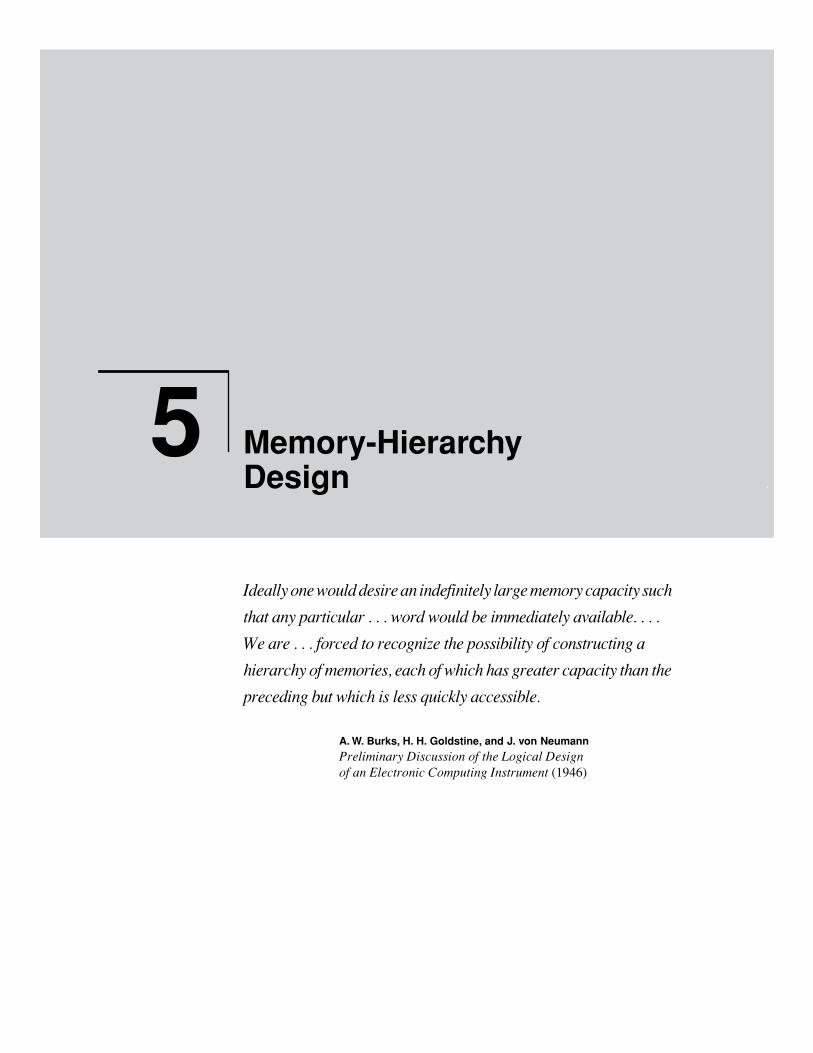
5
Memory-Hierarchy Design
5
Ideally one would desire an indefinitely large memory capacity such
that any particular . . . word would be immediately available. . . .
We are . . . forced to recognize the possibility of constructing a
hierarchy of memories, each of which has greater capacity than the
preceding but which is less quickly accessible.
A. W. Burks, H. H. Goldstine, and J. von Neumann
Preliminary Discussion of the Logical Designof an Electronic Computing Instrument
(1946)
5.1 Introduction 373
5.2 Review of the ABCs of Caches 376
5.3 Cache Performance 390
5.4 Reducing Cache Miss Penalty 398
5.5 Reducing Miss Rate 408
5.6 Reducing Cache Miss Penalty or Miss Rate via Parallelism 421
5.7 Reducing Hit Time 430
5.8 Main Memory and Organizations for Improving Performance 435
5.9 Memory Technology 442
5.10 Virtual Memory 448
5.11 Protection and Examples of Virtual Memory 457
5.12 Crosscutting Issues in the Design of Memory Hierarchies 467
5.13 Putting It All Together: Alpha 21264 Memory Hierarchy 471
5.14 Another View: The Emotion Engine of the Sony Playstation 2 479
5.15 Another View: The Sun Fire 6800 Server 483
5.16 Fallacies and Pitfalls 488
5.17 Concluding Remarks 495
5.18 Historical Perspective and References 498
Exercises 504
Computer pioneers correctly predicted that programmers would want unlimitedamounts of fast memory. An economical solution to that desire is a
memory hier-archy
, which takes advantage of locality and cost/performance of memorytechnologies. The
principle of locality
, presented in the first chapter, says thatmost programs do not access all code or data uniformly (see section 1.6, page38). This principle, plus the guideline that smaller hardware is faster, led to hier-archies based on memories of different speeds and sizes. Figure 5.1 shows a mul-tilevel memory hierarchy, including typical sizes and speeds of access.
Since fast memory is expensive, a memory hierarchy is organized into severallevels—each smaller, faster, and more expensive per byte than the next lower lev-el. The goal is to provide a memory system with cost almost as low as the cheap-est level of memory and speed almost as fast as the fastest level. The levels of thehierarchy usually subset one another. All data in one level is also found in the lev-el below, and all data in that lower level is found in the one below it, and so onuntil we reach the bottom of the hierarchy.
5.1
Introduction
374
Chapter 5 Memory-Hierarchy Design
Note that each level maps addresses from a slower, larger memory to a smallerbut faster memory higher in the hierarchy. As part of address mapping, the mem-ory hierarchy is given the responsibility of address checking; hence protectionschemes for scrutinizing addresses are also part of the memory hierarchy.
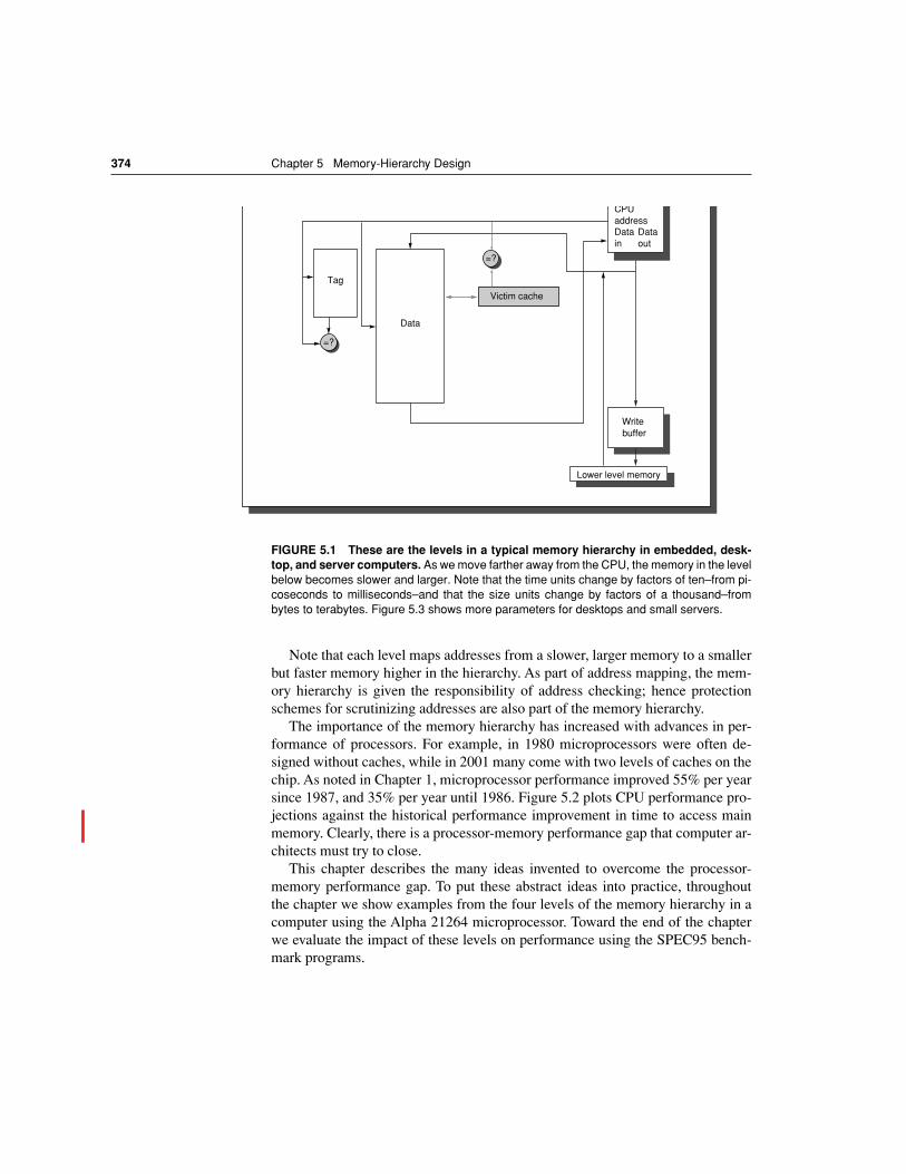
The importance of the memory hierarchy has increased with advances in per-formance of processors. For example, in 1980 microprocessors were often de-signed without caches, while in 2001 many come with two levels of caches on thechip. As noted in Chapter 1, microprocessor performance improved 55% per yearsince 1987, and 35% per year until 1986. Figure 5.2 plots CPU performance pro-jections against the historical performance improvement in time to access mainmemory. Clearly, there is a processor-memory performance gap that computer ar-chitects must try to close.
This chapter describes the many ideas invented to overcome the processor-memory performance gap. To put these abstract ideas into practice, throughoutthe chapter we show examples from the four levels of the memory hierarchy in acomputer using the Alpha 21264 microprocessor. Toward the end of the chapterwe evaluate the impact of these levels on performance using the SPEC95 bench-mark programs.
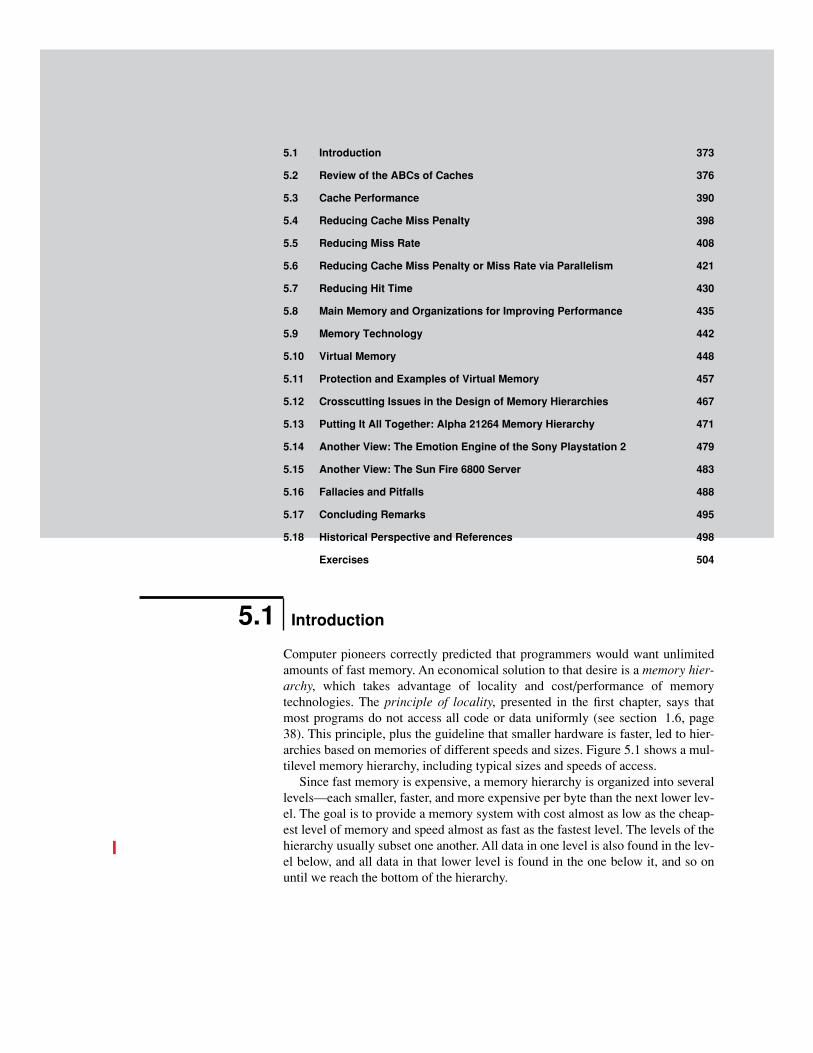
FIGURE 5.1 These are the levels in a typical memory hierarchy in embedded, desk-top, and server computers.
As we move farther away from the CPU, the memory in the levelbelow becomes slower and larger. Note that the time units change by factors of ten–from pi-coseconds to milliseconds–and that the size units change by factors of a thousand–frombytes to terabytes. Figure 5.3 shows more parameters for desktops and small servers.
CPUaddressDatain
Data out
Write buffer
Lower level memory
Tag
Data
Victim cache
=?
=?
5.1 Introduction
375
The 21264 is a microprocessor designed for desktop and servers. Even thesetwo related classes of computers have different concerns in a memory hierarchy.Desktop computers are primarily running one application at a time on top of anoperating system for a single user, whereas server computers may typically havehundreds of users potentially running potentially dozens of applications simulta-neously. These characteristics result in more context switches, which effectivelyincreases compulsory miss rates. Thus, desktop computers are concerned morewith average latency from the memory hierarchy whereas server computers arealso concerned about memory bandwidth. Although protection is important ondesktop computers to deter programs from clobbering each other, server comput-ers must prevent one user from accessing another’s data, and hence the impor-tance of protection escalates. Server computers also tend to be much larger, withmore memory and disk storage, and hence often run much larger applications. In2001 virtually all servers can be purchased as multiprocessors with hundreds ofdisks, which places even greater bandwidth demands on the memory hierarchy.
The memory hierarchy of the embedded computers is often quite differentfrom that of the desktop and server. First, embedded computers are often used inreal-time applications, and hence programmers must worry about worst case per-
FIGURE 5.2 Starting with 1980 performance as a baseline, the gap in performance be-tween memory and CPUs are plotted over time.
Note that the vertical axis must be on alogarithmic scale to record the size of the CPU-DRAM performance gap. The memory base-line is 64-KB DRAM in 1980, with three years to the next generation and a 7% per year per-formance improvement in latency (see Figure 5.30 on page 444). The CPU line assumes a1.35 improvement per year until 1986, and a 1.55 improvement thereafter.
<<NOTE: Artistcontinue the X-axis to 2005: DRAM should be 5.4 in 2005, and CPU should be 25,000 in2005. This means the Y-axis needs to be extended to 100,000 to accommodate.>>
10,000
1000
100
10
1
Performance
Year
1980
1981
1982
1983
1984
1985
1986
1987
1988
1989
1990
1991
1992
1993
1994
1995
1996
1997
2000
1998
1999
Memory CPU
376
Chapter 5 Memory-Hierarchy Design
formance. This concern is problematic for caches that improve average case per-formance, but can degrade worst case performance; we’ll mention sometechniques to address this later in the chapter. Second, embedded applications areoften concerned about power and battery life. The best way to save power is tohave less hardware. Hence, embedded computers may not chose hardware-inten-sive optimizations in the quest of better memory hierarchy performance, aswould most desktop and server computers. Third, embedded applications are typ-ically only running one application and use a very simple operating system, ifthey one at all. Hence, the protection role of the memory hierarchy is often di-minished. Finally, the main memory itself may be quite small–less than onemegabyte–and there is often no disk storage.
This chapter is a tour of the general principles of memory hierarchy using thedesktop as the generic example, but we will take detours to point out where thememory hierarchy of servers and embedded computers diverge from the desktop.Towards the end of the chapter we will pause for two views of the memory hier-archy in addition to the Alpha 21264: the Sony Playstation 2 and the Sun Fire6800 server. Our first stop is a review.
Cache: a safe place for hiding or storing things.
Webster’s New World Dictionary of the American Language, Second College Edition
(1976)
This section is a quick review of cache basics, covering the following 36 terms:
5.2
Review of the ABCs of Caches
cache cache hit cache miss block
virtual memory page page fault page fault
memory stall cycles miss penalty miss rate address trace
direct mapped fully associative n-way set associative set
valid bit dirty bit least-recently used random replacement
block address block offset tag field index
write through
write back write allocate no-write allocate
instruction cache data cache unified cache write buffer
average memory access time
hit time misses per instruction
write stall
5.2 Review of the ABCs of Caches
377
Readers who know the meaning of such terms should skip to “An Example: TheAlpha 21264 Data Cache” on page 387, or even further to section 5.3 on page390 about cache performance. (If this review goes too quickly, you might want tolook at Chapter 7 in
Computer Organization and Design
, which we wrote forreaders with less experience.)
For those interested in a review, two particularly important levels of the mem-ory hierarchy are cache and virtual memory.
Cache
is the name given to the first level of the memory hierarchy encoun-tered once the address leaves the CPU. Since the principle of locality applies atmany levels, and taking advantage of locality to improve performance is popular,the term
cache
is now applied whenever buffering is employed to reuse common-ly occurring items. Examples include
file caches
,
name caches
, and so on. When the CPU finds a requested data item in the cache, it is called a
cache hit
.When the CPU does not find a data item it needs in the cache, a
cache miss
oc-curs. A fixed-size collection of data containing the requested word, called a
block
,is retrieved from the main memory and placed into the cache.
Temporal locality
tells us that we are likely to need this word again in the near future, so it is usefulto place it in the cache where it can be accessed quickly. Because of
spatial local-ity
, there is high probability that the other data in the block will be needed soon. The time required for the cache miss depends on both the latency and band-
width of the memory. Latency determines the time to retrieve the first word of theblock, and bandwidth determines the time to retrieve the rest of this block. Acache miss is handled by hardware and causes processors following in-order exe-cution to pause, or stall, until the data are available.
Similarly, not all objects referenced by a program need to reside in main memo-ry. If the computer has
virtual memory
, then some objects may reside on disk. Theaddress space is usually broken into fixed-size blocks, called
pages
. At any time,each page resides either in main memory or on disk. When the CPU references anitem within a page that is not present in the cache or main memory, a
page fault
oc-curs, and the entire page is moved from the disk to main memory. Since page faultstake so long, they are handled in software and the CPU is not stalled. The CPUusually switches to some other task while the disk access occurs. The cache andmain memory have the same relationship as the main memory and disk.
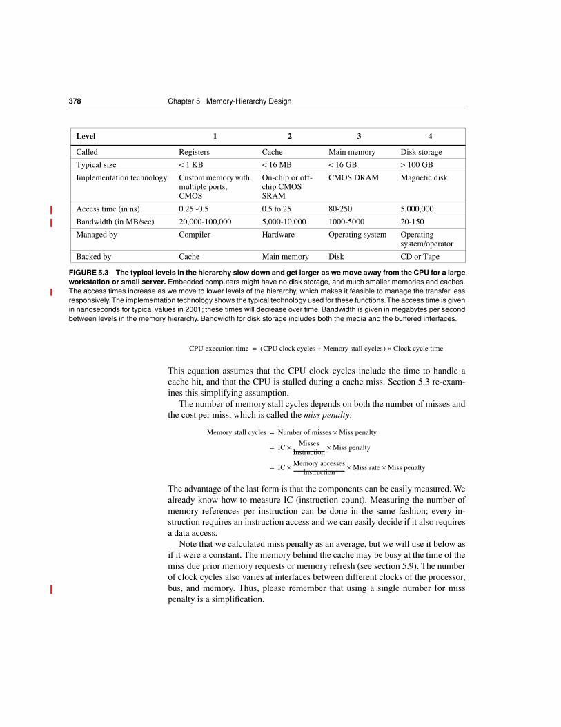
Figure 5.3 shows the range of sizes and access times of each level in the mem-ory hierarchy for computers ranging from high-end desktops to low-end servers.
Cache Performance Review
Because of locality and the higher speed of smaller memories, a memory hierar-chy can substantially improve performance. One method to evaluate cache per-formance is to expand our CPU execution time equation from Chapter 1. We nowaccount for the number of cycles during which the CPU is stalled waiting for amemory access, which we call the
memory stall cycles
. The performance is thenthe product of the clock cycle time and the sum of the CPU cycles and the memo-ry stall cycles:
378
Chapter 5 Memory-Hierarchy Design
This equation assumes that the CPU clock cycles include the time to handle acache hit, and that the CPU is stalled during a cache miss. Section 5.3 re-exam-ines this simplifying assumption.
The number of memory stall cycles depends on both the number of misses andthe cost per miss, which is called the
miss penalty
:
The advantage of the last form is that the components can be easily measured. Wealready know how to measure IC (instruction count). Measuring the number ofmemory references per instruction can be done in the same fashion; every in-struction requires an instruction access and we can easily decide if it also requiresa data access.
Note that we calculated miss penalty as an average, but we will use it below asif it were a constant. The memory behind the cache may be busy at the time of themiss due prior memory requests or memory refresh (see section 5.9). The numberof clock cycles also varies at interfaces between different clocks of the processor,bus, and memory. Thus, please remember that using a single number for misspenalty is a simplification.
Level 1 2 3 4
Called Registers Cache Main memory Disk storage
Typical size < 1 KB < 16 MB < 16 GB > 100 GB
Implementation technology Custom memory with multiple ports, CMOS
On-chip or off-chip CMOS SRAM
CMOS DRAM Magnetic disk
Access time (in ns) 0.25 -0.5 0.5 to 25 80-250 5,000,000
Bandwidth (in MB/sec) 20,000-100,000 5,000-10,000 1000-5000 20-150
Managed by Compiler Hardware Operating system Operatingsystem/operator
Backed by Cache Main memory Disk CD or Tape
FIGURE 5.3 The typical levels in the hierarchy slow down and get larger as we move away from the CPU for a largeworkstation or small server.
Embedded computers might have no disk storage, and much smaller memories and caches.The access times increase as we move to lower levels of the hierarchy, which makes it feasible to manage the transfer lessresponsively. The implementation technology shows the typical technology used for these functions. The access time is givenin nanoseconds for typical values in 2001; these times will decrease over time. Bandwidth is given in megabytes per secondbetween levels in the memory hierarchy. Bandwidth for disk storage includes both the media and the buffered interfaces.
CPU execution time CPU clock cycles Memory stall cycles+( ) Clock cycle time×=
Memory stall cycles Number of misses Miss penalty×=
ICMisses
Instruction-------------------------- Miss penalty××=
ICMemory accesses
Instruction------------------------------------------ Miss rate× Miss penalty××=
5.2 Review of the ABCs of Caches
379
The component
miss rate
is simply the fraction of cache accesses that result ina miss (i.e., number of accesses that miss divided by number of accesses). Missrates can be measured with cache simulators that take an
address trace
of the in-struction and data references, simulate the cache behavior to determine whichreferences hit and which miss, and then report the hit and miss totals. Some mi-croprocessors provide hardware to count the number of misses and memory ref-erences, which is a much easier and faster way to measure miss rate.
The formula above is an approximation since the miss rates and miss penaltiesare often different for reads and writes. Memory stall clock cycles could then bedefined in terms of the number of memory accesses per instruction, miss penalty(in clock cycles) for reads and writes, and miss rate for reads and writes:
Memory stall clock cycles = IC
×
Reads per instruction
×
Read miss rate
×
Read miss penalty
+ IC
×
Writes per instruction
×
Write miss rate
×
Write miss penalty
We normally simplify the complete formula by combining the reads and writesand finding the average miss rates and miss penalty for reads
and
writes:
Memory stall clock cycles = IC
×
×
Miss rate
×
Miss penalty
The miss rate is one of the most important measures of cache design, but, as wewill see in later sections, not the only measure.
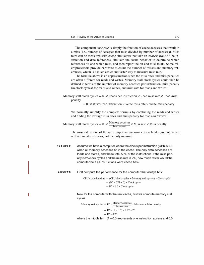
E X A M P L E
Assume we have a computer where the clocks per instruction (CPI) is 1.0 when all memory accesses hit in the cache. The only data accesses are loads and stores, and these total 50% of the instructions. If the miss pen-alty is 25 clock cycles and the miss rate is 2%, how much faster would the computer be if all instructions were cache hits?
A N S W E R
First compute the performance for the computer that always hits:
Now for the computer with the real cache, first we compute memory stall cycles:
where the middle term (1 + 0.5) represents one instruction access and 0.5
Memory accessesInstruction------------------------------------------
CPU execution time CPU clock cycles Memory stall cycles+( ) Clock cycle×=
IC CPI× 0+( ) Clock cycle×=
IC 1.0 Clock cycle××=
Memory stall cycles ICMemory accesses
Instruction------------------------------------------ Miss rate× Miss penalty××=
IC 1 0.5+( ) 0.02 25×××=
IC 0.75×=
380
Chapter 5 Memory-Hierarchy Design
data accesses per instruction. The total performance is thus
The performance ratio is the inverse of the execution times:
The computer with no cache misses is 1.75 times faster.
n
Some designers prefer measuring miss rate as
misses per instruction
ratherthan misses per memory reference. These two are related:
The latter formula is useful when you know the average number of memoryaccesses per instruction as it allows you to convert miss rate into misses per in-struction, and vice versa. For example, we can turn the miss rate per memory ref-erence in the example above into misses per instruction:
By the way, misses per instruction are often reported as misses per 1000 in-structions to show integers instead of fractions. Thus, the answer above couldalso be expressed as 30 misses per 1000 instructions.
The advantage of misses per instruction is that it is independent of the hard-ware implementation. For example, the 21264 fetches about twice as many in-structions as are actually committed, which can artificially reduce the miss rate ifmeasured as misses per memory reference rather than per instruction. The draw-back is that misses per instruction is architecture dependent; for example, the av-erage number of memory accesses per instruction may be very different for an80x86 versus MIPS. Thus, misses per instruction are most popular with architectsworking with a single computer family, although the similarity of RISC architec-tures allows one to give insights into others.
E X A M P L E
To show equivalency between the two miss rate equations, let’s redo the example above, this time assuming a miss rate per 1000 instructions of 30. What is memory stall time in terms of instruction count?
CPU execution timecache IC 1.0× IC 0.75×+( ) Clock cycle×=
1.75 IC Clock cycle××=
CPU execution timecache
CPU execution time-----------------------------------------------------------1.75 IC Clock cycle××1.0 IC Clock cycle××---------------------------------------------------------
=
1.75=
MissesInstruction--------------------------
Miss rate Memory accesses×Instruction Count----------------------------------------------------------------------
= Miss rateMemory accesses
Instruction------------------------------------------×=
MissesInstruction--------------------------
Miss rateMemory accesses
Instruction------------------------------------------× 0.02 1.5× 0.030= = =
5.2 Review of the ABCs of Caches
381
A N S W E R
Recomputing the memory stall cycles:
We get the same answer as on page 379.
n
Four Memory Hierarchy Questions
We continue our introduction to caches by answering the four common ques-tions for the first level of the memory hierarchy:
Q1: Where can a block be placed in the upper level? (
Block placement
)
Q2: How is a block found if it is in the upper level? (
Block identification
)
Q3: Which block should be replaced on a miss? (
Block replacement
)
Q4: What happens on a write? (Write strategy)
The answers to these questions help us understand the different trade-offs ofmemories at different levels of a hierarchy; hence we ask these four questions onevery example.
Q1: Where can a block be placed in a cache?Figure 5.4 shows that the restrictions on where a block is placed create three cate-gories of cache organization:
n If each block has only one place it can appear in the cache, the cache is said tobe direct mapped. The mapping is usually
(Block address) MOD (Number of blocks in cache)
n If a block can be placed anywhere in the cache, the cache is said to be fullyassociative.
n If a block can be placed in a restricted set of places in the cache, the cache isset associative. A set is a group of blocks in the cache. A block is first mappedonto a set, and then the block can be placed anywhere within that set. The setis usually chosen by bit selection; that is,
Memory stall cycles Number of misses Miss penalty×=
ICMisses
Instruction-------------------------- Miss penalty××=
IC 1000⁄ MissesInstruction 1000×-------------------------------------------- Miss penalty××=
IC 1000⁄ 30 25××=
IC 1000⁄ 750×=
IC 0.75×=
382 Chapter 5 Memory-Hierarchy Design
(Block address) MOD (Number of sets in cache)
If there are n blocks in a set, the cache placement is called n-way set associative.
The range of caches from direct mapped to fully associative is really a continuumof levels of set associativity. Direct mapped is simply one-way set associative anda fully associative cache with m blocks could be called m-way set associative.Equivalently, direct mapped can be thought of as having m sets and fullyassociative as having one set.
The vast majority of processor caches today are direct mapped, two-way setassociative, or four-way set associative, for reasons we shall see shortly.
FIGURE 5.4 This example cache has eight block frames and memory has 32 blocks.The three options for caches are shown left to right. In fully associative, block 12 from thelower level can go into any of the eight block frames of the cache. With direct mapped, block12 can only be placed into block frame 4 (12 modulo 8). Set associative, which has some ofboth features, allows the block to be placed anywhere in set 0 (12 modulo 4). With two blocksper set, this means block 12 can be placed either in block 0 or in block 1 of the cache. Realcaches contain thousands of block frames and real memories contain millions of blocks. Theset-associative organization has four sets with two blocks per set, called two-way set asso-ciative. Assume that there is nothing in the cache and that the block address in question iden-tifies lower-level block 12.
Fully associative:block 12 can goanywhere
Direct mapped:block 12 can goonly into block 4(12 mod 8)
Set associative:block 12 can goanywhere in set 0(12 mod 4)
0 1 2 3 4 5 6 7 0 1 2 3 4 5 6 7 0 1 2 3 4 5 6 7Block no.
Block no.
Block no.
Set0
Set1
Set2
Set3
1 1 1 1 1 1 1 1 1 1 2 2 2 2 2 2 2 2 2 2 3 30 1 2 3 4 5 6 7 8 9 0 1 2 3 4 5 6 7 8 9 0 1 2 3 4 5 6 7 8 9 0 1
Block
Block frame address
no.
Cache
Memory
5.2 Review of the ABCs of Caches 383
Q2: How is a block found if it is in the cache?Caches have an address tag on each block frame that gives the block address. Thetag of every cache block that might contain the desired information is checked tosee if it matches the block address from the CPU. As a rule, all possible tags aresearched in parallel because speed is critical.
There must be a way to know that a cache block does not have valid informa-tion. The most common procedure is to add a valid bit to the tag to say whether ornot this entry contains a valid address. If the bit is not set, there cannot be a matchon this address.
Before proceeding to the next question, let’s explore the relationship of a CPUaddress to the cache. Figure 5.5 shows how an address is divided. The first divi-sion is between the block address and the block offset. The block frame addresscan be further divided into the tag field and the index field. The block-offset fieldselects the desired data from the block, the index field selects the set, and the tagfield is compared against it for a hit. Although the comparison could be made onmore of the address than the tag, there is no need because of the following:
n The offset should not be used in the comparison, since the entire block ispresent or not, and hence all block offsets result in a match by definition.
n Checking the index is redundant, since it was used to select the set to bechecked. An address stored in set 0, for example, must have 0 in the index fieldor it couldn’t be stored in set 0; set 1 must have an index value of 1; and so on.This optimization saves hardware and power by reducing the width of memorysize for the cache tag.
If the total cache size is kept the same, increasing associativity increases thenumber of blocks per set, thereby decreasing the size of the index and increasingthe size of the tag. That is, the tag-index boundary in Figure 5.5 moves to theright with increasing associativity, with the end point of fully associative cacheshaving no index field.
FIGURE 5.5 The three portions of an address in a set-associative or direct-mappedcache. The tag is used to check all the blocks in the set and the index is used to select theset. The block offset is the address of the desired data within the block. Fully associativecaches have no index field.
Tag IndexBlockoffset
Block address
384 Chapter 5 Memory-Hierarchy Design
Q3: Which block should be replaced on a cache miss? When a miss occurs, the cache controller must select a block to be replaced withthe desired data. A benefit of direct-mapped placement is that hardware decisionsare simplified—in fact, so simple that there is no choice: Only one block frame ischecked for a hit, and only that block can be replaced. With fully associative orset-associative placement, there are many blocks to choose from on a miss. Thereare three primary strategies employed for selecting which block to replace:
n Random—To spread allocation uniformly, candidate blocks are randomlyselected. Some systems generate pseudorandom block numbers to get repro-ducible behavior, which is particularly useful when debugging hardware.
n Least-recently used (LRU)—To reduce the chance of throwing out informationthat will be needed soon, accesses to blocks are recorded. Relying on the pastto predict the future, the block replaced is the one that has been unused for thelongest time. LRU relies on a corollary of locality: If recently used blocks arelikely to be used again, then a good candidate for disposal is the least-recentlyused block.
n First In First Out (FIFO)—Because LRU can be complicated to calculate, thisapproximates LRU by determining the oldest block rather than the LRU.
A virtue of random replacement is that it is simple to build in hardware. As thenumber of blocks to keep track of increases, LRU becomes increasingly ex-pensive and is frequently only approximated. Figure 5.6 shows the difference inmiss rates between LRU, random, and FIFO replacement.
Q4: What happens on a write?Reads dominate processor cache accesses. All instruction accesses are reads, andmost instructions don’t write to memory. Figure 2.32 on page 149 in Chapter 2
Associativity
Two-way Four-way Eight-way
Size LRU Random FIFO LRU Random FIFO LRU Random FIFO
16 KB 114.1 117.3 115.5 111.7 115.1 113.3 109.0 111.8 110.4
64 KB 103.4 104.3 103.9 102.4 102.3 103.1 99.7 100.5 100.3
256 KB 92.2 92.1 92.5 92.1 92.1 92.5 92.1 92.1 92.5
FIGURE 5.6 Data cache misses per 1000 instructions comparing least-recently used, random, and first-in, first-outreplacement for several sizes and associativities. There is little difference between LRU and random for the largest-sizecache, with LRU outpeforming the others for smaller caches. FIFO generally outperforms random in the smaller cache sizes.These data were collected for a block size of 64 bytes for the Alpha architecture using ten SPEC2000 benchmarks. Five arefrom SPECint2000 (gap, gcc, gzip, mcf, and perl) and five are from SPECfp2000 (applu, art, equake, lucas, and swim). Wewill use this computer and these benchmarks in most figures in this chapter.
5.2 Review of the ABCs of Caches 385
suggests a mix of 10% stores and 37% loads for MIPS programs, making writes10%/(100% + 37% + 10%) or about 7% of the overall memory traffic. Of thedata cache traffic, writes are 10%/(37% + 10%) or about 21%. Making the com-mon case fast means optimizing caches for reads, especially since processors tra-ditionally wait for reads to complete but need not wait for writes. Amdahl’s Law(section 1.6, page 29) reminds us, however, that high-performance designs can-not neglect the speed of writes.
Fortunately, the common case is also the easy case to make fast. The block canbe read from cache at the same time that the tag is read and compared, so theblock read begins as soon as the block address is available. If the read is a hit, therequested part of the block is passed on to the CPU immediately. If it is a miss,there is no benefit—but also no harm in desktop and server computers; just ig-nore the value read. Embedded’s emphasis on power generally means avoidingunnecessary work, which might lead the designer to separate data read from ad-dress check so that data is not read on a miss.
Such optimism is not allowed for writes. Modifying a block cannot begin untilthe tag is checked to see if the address is a hit. Because tag checking cannot occurin parallel, writes normally take longer than reads. Another complexity is that theprocessor also specifies the size of the write, usually between 1 and 8 bytes; onlythat portion of a block can be changed. In contrast, reads can access more bytesthan necessary without fear; once again, embedded designers might weigh thepower benefits of reading less.
The write policies often distinguish cache designs. There are two basic optionswhen writing to the cache:
n Write through —The information is written to both the block in the cache andto the block in the lower-level memory.
n Write back —The information is written only to the block in the cache. Themodified cache block is written to main memory only when it is replaced.
To reduce the frequency of writing back blocks on replacement, a featurecalled the dirty bit is commonly used. This status bit indicates whether the blockis dirty (modified while in the cache) or clean (not modified). If it is clean, theblock is not written back on a miss, since identical information to the cache isfound in lower levels.
Both write back and write through have their advantages. With write back,writes occur at the speed of the cache memory, and multiple writes within a blockrequire only one write to the lower-level memory. Since some writes don’t go tomemory, write back uses less memory bandwidth, making write back attractive inmultiprocessors which are common in servers. Since write back uses the rest ofthe memory hierarchy and memory buses less than write through, it also savespower, making it attractive for embedded applications.
Write through is easier to implement than write back. The cache is alwaysclean, so unlike write back read misses never result in writes to the lower level.Write through also has the advantage that the next lower level has the most cur-rent copy of the data, which simplifies data coherency. Data coherency (see sec-
386 Chapter 5 Memory-Hierarchy Design
tion 5.12) is important for multiprocessors and for I/O, which we examine inChapters 6 and 7.
As we shall see, I/O and multiprocessors are fickle: they want write back forprocessor caches to reduce the memory traffic and write through to keep thecache consistent with lower levels of the memory hierarchy.
When the CPU must wait for writes to complete during write through, theCPU is said to write stall. A common optimization to reduce write stalls is a writebuffer, which allows the processor to continue as soon as the data is written to thebuffer, thereby overlapping processor execution with memory updating. As weshall see shortly, write stalls can occur even with write buffers.
Since the data are not needed on a write, there are two are two options on awrite miss:
n Write allocate —The block is allocated on a write miss, followed by the write-hit actions above. In this natural option, write misses act like read misses.
n No-write allocate—This apparently unusual alternative is write misses do notaffect the cache. Instead, the block is modified only in the lower level memory.
Thus, blocks stays out of the cache in no-write allocate until the program tries toread the blocks, but even blocks that are only written will still be in the cache withwrite allocate. Let’s look at an example.
E X A M P L E Assume a fully associative write back cache with many cache entries that starts empty. Below is a sequence of five memory operations (the address is in parentheses):
Write Mem[100];WriteMem[100];Read Mem[200];WriteMem[200];WriteMem[100].
What are the number of hits and misses with using no-write allocate ver-sus write allocate?
A N S W E R For no-write allocate, the address 100 is not in the cache, and there is no allocation on write, so the first two writes will result in misses. Address 200 is also not in the cache, so the read is also a miss. The subsequent write to address 200 is a hit. The last write to 100 is still a miss. The result for no write allocate is 4 misses and 1 hit.
For write allocate, the first accesses to 100 and 200 are misses, and the rest are hits since 100 and 200 are both found in the cache. Thus, the re-sult for write allocate is 2 misses and 3 hits. n
5.2 Review of the ABCs of Caches 387
Either write-miss policy could be used with write through or write back. Normal-ly, write-back caches use write allocate, hoping that subsequent writes to that blockwill be captured by the cache. Write-through caches often use no-write allocate. Thereasoning is that even if there are subsequent writes to that block, the writes muststill go to the lower level memory, so what’s to be gained?
An Example: The Alpha 21264 Data Cache
To give substance to these ideas, Figure 5.7 shows the organization of the datacache in the Alpha 21264 microprocessor that is found in the Compaq AlphaSer-ver ES40, one of several models that use it. The cache contains 65,536 (64K)bytes of data in 64-byte blocks with two-way set-associative placement, writeback, and write allocate on a write miss.
Let’s trace a cache hit through the steps of a hit as labeled in Figure 5.7. (Thefour steps are shown as circled numbers.) As we shall see later (Figure 5.36), the21264 processor presents a 48-bit virtual address to the cache for tag comparison,which is simultaneously translated into a 44-bit physical address. (It also option-ally supports 43-bit virtual addresses with 41-bit physical addresses.)
The reason Alpha doesn’t use all 64 bits of virtual address is that its designersdon’t think anyone needs that big of virtual address space yet, and the smallersize simplifies the Alpha virtual address mapping. The designers planned to growthe virtual address in future microprocessors.
The physical address coming into the cache is divided into two fields: the 38-bit block address and 6-bit block offset (64 = 26 and 38 + 6 = 44). The block ad-dress is further divided into an address tag and cache index. Step 1 shows this di-vision.
The cache index selects the tag to be tested to see if the desired block is in thecache. The size of the index depends on cache size, block size, and set associativ-ity. For the 21264 cache the set associativity is set to two, and we calculate the in-dex as follows:
Hence, the index is 9 bits wide, and the tag is 38 – 9 or 29 bits wide. Althoughthat is the index needed to select the proper block, 64 bytes is much more than theCPU wants to consume at once. Hence, it makes more sense to organize the dataportion of the cache memory 8 bytes wide, which is the natural data word of the64-bit Alpha processor. Thus, in addition to 9 bits to index the proper cacheblock, 3 more bits from the block offset are used to index the proper 8 bytes.
Index selection is step 2 in Figure 5.7. The two tags are compared and thewinner is selected. (Section 5.10 explains how the 21264 handles virtual addresstranslation.)
2index Cache size
Block size Set associativity×----------------------------------------------------------------------6553664 2×---------------
512 29
= = ==
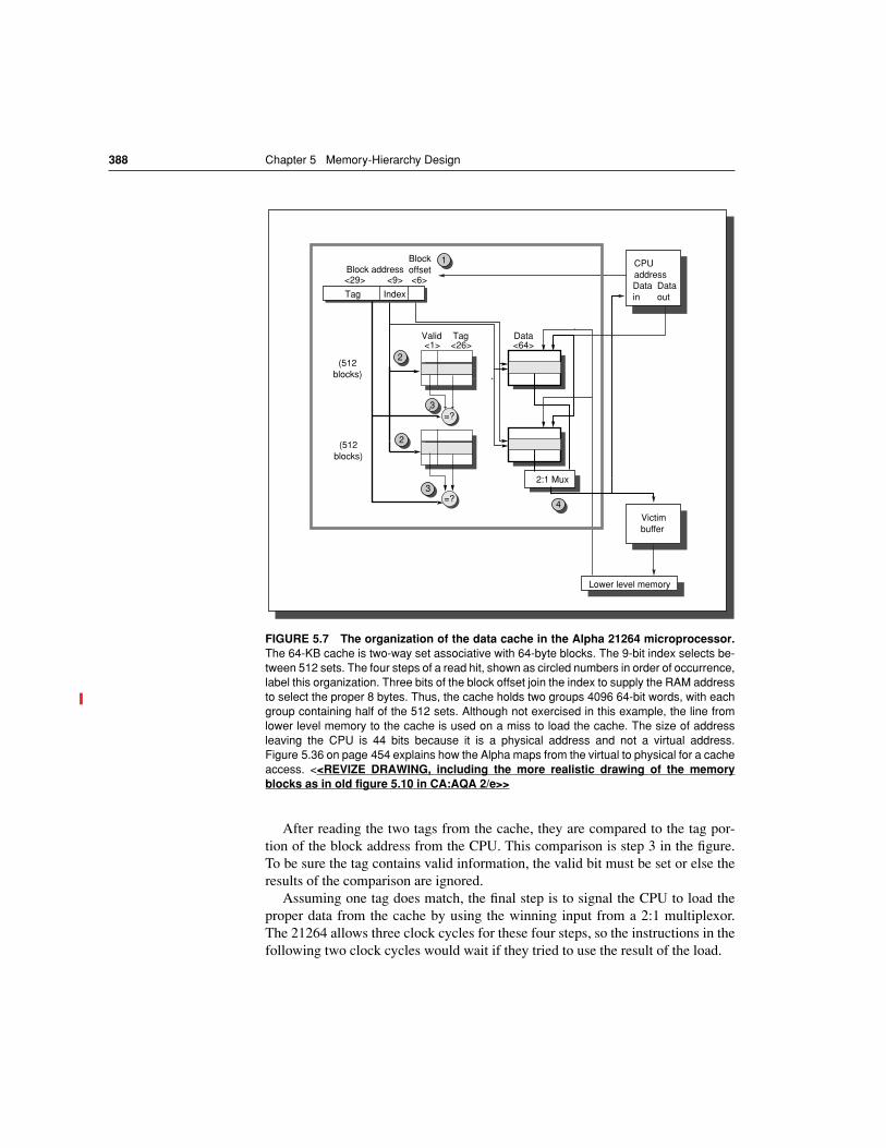
388 Chapter 5 Memory-Hierarchy Design
After reading the two tags from the cache, they are compared to the tag por-tion of the block address from the CPU. This comparison is step 3 in the figure.To be sure the tag contains valid information, the valid bit must be set or else theresults of the comparison are ignored.
Assuming one tag does match, the final step is to signal the CPU to load theproper data from the cache by using the winning input from a 2:1 multiplexor.The 21264 allows three clock cycles for these four steps, so the instructions in thefollowing two clock cycles would wait if they tried to use the result of the load.
FIGURE 5.7 The organization of the data cache in the Alpha 21264 microprocessor.The 64-KB cache is two-way set associative with 64-byte blocks. The 9-bit index selects be-tween 512 sets. The four steps of a read hit, shown as circled numbers in order of occurrence,label this organization. Three bits of the block offset join the index to supply the RAM addressto select the proper 8 bytes. Thus, the cache holds two groups 4096 64-bit words, with eachgroup containing half of the 512 sets. Although not exercised in this example, the line fromlower level memory to the cache is used on a miss to load the cache. The size of addressleaving the CPU is 44 bits because it is a physical address and not a virtual address.Figure 5.36 on page 454 explains how the Alpha maps from the virtual to physical for a cacheaccess. <<REVIZE DRAWING, including the more realistic drawing of the memoryblocks as in old figure 5.10 in CA:AQA 2/e>>
Block addressBlockoffset
CPUaddressDatain
Dataout
<29>
Tag Index
<9> <6>
4
3
3
(512blocks)
(512blocks)
2
2
1
Victimbuffer
Lower level memory
Valid Data<1> <26> <64>
=?
Tag
2:1 Mux
=?
5.2 Review of the ABCs of Caches 389
Handling writes is more complicated than handling reads in the 21264, as it isin any cache. If the word to be written is in the cache, the first three steps are thesame. Since the 21264 executes out-of-order, only after it signals that the instruc-tion has committed and the cache tag comparison indicates a hit are the data arewritten to the cache.
So far we have assumed the common case of a cache hit. What happens on amiss? On a read miss, the cache sends a signal to the processor telling it the datais not yet available, and 64 bytes are read from the next level of the hierarchy. Thepath to the next lower level in the 21264 is 16 bytes wide. In the 667 MHz Al-phaServer ES40 it takes 2.25 ns per transfer, or 9 ns for all 64 bytes. Since thedata cache is set associative, there is a choice on which block to replace. The21264 does round robin selection, dedicating a bit for every two blocks to re-member where to go next. Unlike LRU, which selects the block that was refer-enced longest ago, round robin selects the block that was filled longest ago.Round robin is easier to implement since it is only updated on a miss rather thanon every hit. Replacing a block means updating the data, the address tag, the val-id bit, and the round robin bit.
Since the 21264 uses write back, the old data block could have been modified,and hence it cannot simply be discarded. The 21264 keeps one dirty bit per blockto record if the block was written. If the “victim” was modified, its data and ad-dress are sent to the Victim Buffer. (This structure is similar to a write buffer inother computers.) The 21264 has space for eight victim blocks. In parallel withother cache actions, it writes victim blocks to the next level of the hierarchy. Ifthe Victim Buffer is full, the cache must wait.
A write miss is very similar to a read miss, since the 21264 allocates a blockon a read or a write miss.
We have seen how it works, but the data cache cannot supply all the memoryneeds of the processor: the processor also needs instructions. Although a singlecache could try to supply both, it can be a bottleneck. For example, when a loador store instruction is executed, the pipelined processor will simultaneously re-quest both a data word and an instruction word. Hence, a single cache wouldpresent a structural hazard for loads and stores, leading to stalls. One simple wayto conquer this problem is to divide it: one cache is dedicated to instructions andanother to data. Separate caches are found in most recent processors, includingthe Alpha 21264. Hence, it has a 64-KB instruction cache as well as the 64-KBdata cache.
The CPU knows whether it is issuing an instruction address or a data address,so there can be separate ports for both, thereby doubling the bandwidth betweenthe memory hierarchy and the CPU. Separate caches also offer the opportunity ofoptimizing each cache separately: different capacities, block sizes, and associa-tivities may lead to better performance. (In contrast to the instruction caches anddata caches of the 21264, the terms unified or mixed are applied to caches that cancontain either instructions or data.)
390 Chapter 5 Memory-Hierarchy Design
Figure 5.8 shows that instruction caches have lower miss rates than datacaches. Separating instructions and data removes misses due to conflicts betweeninstruction blocks and data blocks, but the split also fixes the cache space devotedto each type. Which is more important to miss rates? A fair comparison of sepa-rate instruction and data caches to unified caches requires the total cache size tobe the same. For example, a separate 16-KB instruction cache and 16-KB datacache should be compared to a 32-KB unified cache. Calculating the averagemiss rate with separate instruction and data caches necessitates knowing the per-centage of memory references to each cache. Figure 2.32 on page 149 suggeststhe split is 100%/(100% + 37% + 10%) or about 78% instruction references to(37% + 10%)/(100% + 37% + 10%) or about 22% data references. Splitting af-fects performance beyond what is indicated by the change in miss rates, as weshall see shortly.
Because instruction count is independent of the hardware, it is tempting to evalu-ate CPU performance using that number. As we saw in Chapter 1, however, suchindirect performance measures have waylaid many a computer designer. Thecorresponding temptation for evaluating memory-hierarchy performance is to con-centrate on miss rate, because it, too, is independent of the speed of the hardware.As we shall see, miss rate can be just as misleading as instruction count. A bettermeasure of memory-hierarchy performance is the average memory access time:
Average memory access time = Hit time + Miss rate × Miss penalty
where Hit time is the time to hit in the cache; we have seen the other two terms be-fore. The components of average access time can be measured either in absolutetime—say, 0.25 to 1.0 nanoseconds on a hit—or in the number of clock cycles that
Size Instruction cache Data cache Unified cache
8 KB 8.16 44.0 63.0
16 KB 3.82 40.9 51.0
32 KB 1.36 38.4 43.3
64 KB 0.61 36.9 39.4
128 KB 0.30 35.3 36.2
256 KB 0.02 32.6 32.9
FIGURE 5.8 Miss per 1000 instructions for instruction, data, and unified caches of dif-ferent sizes. The percentage of instruction references is about 78%. The data are for two-way associative caches with 64-byte blocks for the same computer and benchmarks as Fig-ure 5.6.
5.3 Cache Performance
5.3 Cache Performance 391
the CPU waits for the memory—such as a miss penalty of 75 to 100 clock cycles.Remember that average memory access time is still an indirect measure of perfor-mance; although it is a better measure than miss rate, it is not a substitute for exe-cution time.
This formula can help us decide between split caches and a unified cache.
E X A M P L E Which has the lower miss rate: a 16-KB instruction cache with a 16-KB data cache or a 32-KB unified cache? Use the miss rates in Figure 5.7 to help calculate the correct answer assuming 47% of the instructions are data transfer instructions. Assume a hit takes 1 clock cycle and the miss penalty is 100 clock cycles. A load or store hit takes 1 extra clock cycle on a unified cache if there is only one cache port to satisfy two simultaneous requests. Using the pipelining terminology of the previous chapter, the unified cache leads to a structural hazard. What is the average memory access time in each case? Assume write-through caches with a write buff-er and ignore stalls due to the write buffer.
A N S W E R First let’s convert misses per 1000 instructions into miss rates. Solving the general formula is from above, miss rate is
Since every instruction access has exactly 1 memory access to fetch the instruction, the instruction miss rate is:
Since 47% of the instructions are data transfers, the data miss rate is:
The unified miss rate needs to account for instruction and data accesses:
As stated above, about 78% of the memory accesses are instruction references. Thus, the overall miss rate for the split caches is
(78% × 0.004) + (22% × 0.087) = 0.022
Miss rate
Misses1000 Instructions----------------------------------------- 1000⁄
Memory accessesInstruction------------------------------------------
----------------------------------------------------------=
Miss rate16 KB Instruction3.82 1000⁄
1.00-------------------------- 0.004==
Miss rate16 KB Data40.9 1000⁄
0.47-------------------------- 0.087==
Miss rate32 KB Unified43.3 1000⁄1.00 0.47+--------------------------- 0.029==
392 Chapter 5 Memory-Hierarchy Design
Thus, a 32-KB unified cache has a higher effective miss rate than two16-KB caches.
The average memory access time formula can be divided into instruction and data accesses:
Therefore, the time for each organization is
Hence, the split caches in this example—which offer two memory ports per clock cycle, thereby avoiding the structural hazard—also have a better average memory access time than the single-ported unified cache. n
Average memory access time and Processor Performance
An obvious question is whether average memory access time due to cache missespredicts processor performance.
First, there are other reasons for stalls, such as contention due to I/O devicesusing memory. Designers often assume that all memory stalls are due to cachemisses, since the memory hierarchy typically dominates other reasons for stalls.We use this simplifying assumption here, but beware to account for all memorystalls when calculating final performance.
Second, the answer depends also on the CPU. If we have an in-order executionCPU (See Chapter 3), then the answer is basically yes. The CPU stalls duringmisses, and the memory stall time is strongly correlated to average memory ac-cess time. Let’s make that assumption for now, but we’ll return to out-of-orderCPUs in the next subsection.
As stated in the prior section, we can model CPU time as:
CPU time = (CPU execution clock cycles + Memory stall clock cycles) × Clock cycle time
This formula raises the question whether the clock cycles for a cache hit shouldbe considered part of CPU execution clock cycles or part of memory stall clockcycles. Although either convention is defensible, the most widely accepted is toinclude hit clock cycles in CPU execution clock cycles.
We can now explore the impact of caches on performance.
Average memory access time
% instructions Hit time Instruction miss rate Miss penalty×+( ) +×=
% data Hit time Data miss rate Miss penalty×+( )×
Average memory access timesplit
78% 1 0.004 100×+( ) 22% 1 0.087 100×+( )×+×=
78% 1.38×( ) 22% 9.70×( )+ 1.078 2.134+ 3.21= = =
Average memory access timeunified
78% 1 0.029 100×+( ) 22% 1 1 0.029 100×+ +( )×+×=
78% 3.95×( ) 22% 4.95×( )+ 3.080 1.089+ 4.17= = =
5.3 Cache Performance 393
E X A M P L E Let’s use an in-order execution computer for the first example, such as the UltraSPARC III (see section 5.15). Assume the cache miss penalty is 100 clock cycles, and all instructions normally take 1.0 clock cycles (ignoring memory stalls). Assume the average miss rate is 2%, there is an average of 1.5 memory references per instruction, and that the average number of cache misses per 1000 instructions is 30. What is the impact on perfor-mance when behavior of the cache is included? Calculate the impact using both misses per instruction and miss rate.
A N S W E R
The performance, including cache misses, is
CPU timewith cache = IC × (1.0 + (30 / 1000 × 100)) × Clock cycle time
= IC × 4.00 × Clock cycle time
Now calculating performance using miss rate:
CPU timewith cache = IC × (1.0 + (1.5 × 2% × 100)) × Clock cycle time
= IC × 4.00 × Clock cycle time
The clock cycle time and instruction count are the same, with or with-out a cache. Thus, CPU time increases fourfold, with CPI from 1.00 for a “perfect cache” to 4.00 with a cache that can miss. Without any memory hierarchy at all the CPI would increase again to 1.0 + 100 × 1.5 or 151—a factor of almost 40 times longer than a system with a cache! n
As this example illustrates, cache behavior can have enormous impact on per-formance. Furthermore, cache misses have a double-barreled impact on a CPUwith a low CPI and a fast clock:
1. The lower the CPIexecution, the higher the relative impact of a fixed number ofcache miss clock cycles.
2. When calculating CPI, the cache miss penalty is measured in CPU clockcycles for a miss. Therefore, even if memory hierarchies for two computers areidentical, the CPU with the higher clock rate has a larger number of clockcycles per miss and hence a higher memory portion of CPI.
CPU time = IC CPIexecutionMemory stall clock cycles
Instruction---------------------------------------------------------------+
× Clock cycle time×
CPU time IC CPIexecution Miss rate+(× Memory accessesInstruction------------------------------------------ Miss penalty××
Clock cycle time×=
394 Chapter 5 Memory-Hierarchy Design
The importance of the cache for CPUs with low CPI and high clock rates is thusgreater, and, consequently, greater is the danger of neglecting cache behavior inassessing performance of such computers. Amdahl’s Law strikes again!
Although minimizing average memory access time is a reasonable goal—andwe will use it in much of this chapter—keep in mind that the final goal is to re-duce CPU execution time. The next example shows how these two can differ.
E X A M P L E What is the impact of two different cache organizations on the perfor-mance of a CPU? Assume that the CPI with a perfect cache is 2.0, the clock cycle time is 1.0 ns, there are 1.5 memory references per instruc-tion, the size of both caches is 64 KB, and both have a block size of 64 bytes. One cache is direct mapped and the other is two-way set associa-tive. Figure 5.7 on page 388 shows that for set-associative caches we must add a multiplexor to select between the blocks in the set depending on the tag match. Since the speed of the CPU is tied directly to the speed of a cache hit, assume the CPU clock cycle time must be stretched 1.25 times to accommodate the selection multiplexor of the set-associative cache. To the first approximation, the cache miss penalty is 75 ns for ei-ther cache organization. (In practice, it is normally rounded up or down to an integer number of clock cycles.) First, calculate the average memory access time, and then CPU performance. Assume the hit time is one clock cycle, the miss rate of a direct-mapped 64-KB cache is 1.4%, and the miss rate for a two-way set-associative cache of the same size is 1.0%.
A N S W E R Average memory access time is
Average memory access time = Hit time + Miss rate × Miss penalty
Thus, the time for each organization is
Average memory access time1-way = 1.0 + (.014 × 75) = 2.05 nsAverage memory access time2-way = 1.0 × 1.25 + (.010 × 75) = 2.00 ns
The average memory access time is better for the two-way set-associative cache.
CPU performance is
Substituting 75 ns for (Miss penalty × Clock cycle time), the performance
CPU time IC CPIExecutionMisses
Instruction-------------------------- Miss penalty× Clock cycle time×+
×=
IC CPIExecution( Clock cycle time )××=
Miss rateMemory accesses
Instruction------------------------------------------ Miss penalty Clock cycle time××× +
5.3 Cache Performance 395
of each cache organization is
and relative performance is
In contrast to the results of average memory access time comparison, the direct-mapped cache leads to slightly better average performance be-cause the clock cycle is stretched for all instructions for the two-way set-associative case, even if there are fewer misses. Since CPU time is our bottom-line evaluation, and since direct mapped is simpler to build, the preferred cache is direct mapped in this example. n
Miss Penalty and Out-of-Order Execution Processors
For an out-of-order execution processor, how do you define miss penalty? Is it thefull latency of the miss to memory, or is it just the “exposed” or non-overlappedlatency when the processor must stall? This question does not arise in processorswhich stall until the data miss completes.
Let’s redefine memory stalls to lead to a new definition of miss penalty as non-overlapped latency:
Similarly, as some out-of-order CPUs stretch the hit time, that portion of the per-formance equation could be divided total hit latency less overlapped hit latency.This equation could be further expanded to account for contention for memoryresources in an out-of-order processor by dividing total miss latency into latencywithout contention and latency due to contention. Let’s just concentrate on misslatency.
We now have to decide
n length of memory latency: what to consider as the start and the end of a memoryoperation in an out-of-order processor; and
n length of latency overlap: what is the start of overlap with for the processor (orequivalently, when do we say a memory operation is stalling the processor).
Given the complexity of out-of-order execution processors, there is no single cor-rect definition.
CPU time1-way IC 2 1.0 1.5 0.014 75××( )+×( )× 3.58 IC×= =
CPU time2-way IC 2 1.0 1.25× 1.5 0.010 75××( )+×( )× 3.63 IC×= =
CPU time2-wayCPU time1-way-------------------------------------
3.63 Instruction count×3.58 Instruction count×---------------------------------------------------------
3.633.58---------- 1.01===
Memory stall cyclesInstruction------------------------------------------------
MissesInstruction-------------------------- Total miss latency Overlapped miss latency–( )×=
396 Chapter 5 Memory-Hierarchy Design
Since only committed operations are seen at the retirement pipeline stage, wesay a processor is stalled in a clock cycle if it does not retire the maximum possi-ble number of instructions in that cycle. We attribute that stall to the first instruc-tion that could not be retired. This definition is by no means foolproof. Forexample, applying an optimization to improve a certain stall time may not alwaysimprove execution time because another type of stall—hidden behind the targetedstall—may now be exposed.
For latency, we could start measuring from the time the memory instruction isqueued in the instruction window, or when the address is generated, or when theinstruction is actually sent to the memory system. Any option works as long as itis used in a consistent fashion.
E X A M P L E Let’s redo the example above, but this time assuming the processor with the longer clock cycle time supports out-of-order execution yet still has a direct mapped cache. Assume 30% of the 75 ns miss penalty can be over-lapped; that is, the average CPU memory stall time is now 52.5 ns.
A N S W E R Average memory access time for the out-of-order computer isAverage memory access time1-way,OOO = 1.0 × 1.25+ (0.014 × 52.5) = 1.99 ns
The performance of the OOO cache is
Hence, despite a much slower clock cycle time and the higher miss rate of a direct mapped cache, the out-of-order computer can be slightly faster if it can hide 30% of the miss penalty. n
In summary, although the state-of-the-art in defining and measuring memorystalls for out-of-order processors is not perfect and is relatively complex, readersshould be aware of the issues for they significantly affect performance.
Improving Cache Performance
To help summarize this section and to act as a handy reference, Figure 5.9 liststhe cache equations in this chapter.
The increasing gap between CPU and main memory speeds shown in Figure5.2 has attracted the attention of many architects. A bibliographic search for theyears 1989 to 2001 revealed more than 5000 research papers on the subject ofcaches. Your authors’ job was to survey all 5000 papers, decide what is and is notworthwhile, translate the results into a common terminology, reduce the results totheir essence, write in an intriguing fashion, and provide just the right amount ofdetail!
CPU time1-way,OOO IC 2 1.0 1.25× 1.5 0.014 52.5××( )+×( )× 3.60 IC×= =
5.3 Cache Performance 397
Fortunately, this task was simplified by our long standing policy of only in-cluding ideas in this book that have made their way into commercially viablecomputers. In computer architecture, many ideas look much better on paper thanin silicon.
The average memory access time formula gave us a framework to present thesurviving cache optimizations for improving cache performance or power:
Average memory access time = Hit time + Miss rate × Miss penalty
Hence, we organize 16 cache optimizations into four categories:
n Reducing the miss penalty (Section 5.4): multilevel caches, critical word first,read miss before write miss, merging write buffers, victim caches;
n Reducing the miss rate (Section 5.5): larger block size, larger cache size, higherassociativity, pseudo-associativity, and compiler optimizations;
n Reducing the miss penalty or miss rate via parallelism (Section 5.6): nonblock-ing caches, hardware prefetching, and compiler prefetching;
n Reducing the time to hit in the cache (Section 5.7): small and simple caches,avoiding address translation, and pipelined cache access.
FIGURE 5.9 Summary of performance equations in this chapter. The first equation calculates with cache index size,but the rest help evaluates performance. The final two equations deal with multilevel caches, is explained early in the nextsection. They are included here to help make the figure a useful reference.
2index Cache size
Block size Set associativity×----------------------------------------------------------------------=
CPU execution time CPU clock cycles Memory stall cycles+( ) Clock cycle time×=
Memory stall cycles Number of misses Miss penalty×=
Memory stall cycles ICMisses
Instruction-------------------------- Miss penalty××=
MissesInstruction--------------------------
Miss rateMemory accesses
Instruction------------------------------------------×=
Average memory access time Hit time Miss rate Miss penalty×+=
CPU execution time IC CPIexecutionMemory stall clock cycles
Instruction---------------------------------------------------------------+
× Clock cycle time×=
CPU execution time IC CPIexecutionMisses
Instruction-------------------------- Miss penalty×+ × Clock cycle time×=
CPU execution time IC CPIexecution Miss rateMemory accesses
Instruction------------------------------------------× Miss penalty×+ × Clock cycle time×=
Memory stall cyclesInstruction------------------------------------------------
MissesInstruction-------------------------- Total miss latency Overlapped miss latency–( )×=
Average memory access time Hit timeL1 Miss rateL1 Hit timeL2 Miss rateL2+ Miss penaltyL2×( )×+=
Memory stall cyclesInstruction------------------------------------------------
MissesL1
Instruction-------------------------- Hit timeL2×MissesL2
Instruction-------------------------- Miss penaltyL2×+=
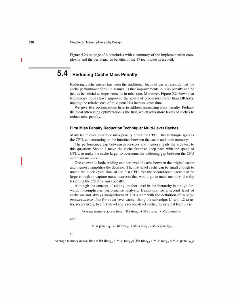
398 Chapter 5 Memory-Hierarchy Design
Figure 5.26 on page 436 concludes with a summary of the implementation com-plexity and the performance benefits of the 17 techniques presented.
Reducing cache misses has been the traditional focus of cache research, but thecache performance formula assures us that improvements in miss penalty can bejust as beneficial as improvements in miss rate. Moreover, Figure 5.2 shows thattechnology trends have improved the speed of processors faster than DRAMs,making the relative cost of miss penalties increase over time.
We give five optimizations here to address increasing miss penalty. Perhapsthe most interesting optimization is the first, which adds more levels of caches toreduce miss penalty.
First Miss Penalty Reduction Technique: Multi-Level Caches
Many techniques to reduce miss penalty affect the CPU. This technique ignoresthe CPU, concentrating on the interface between the cache and main memory.
The performance gap between processors and memory leads the architect tothis question: Should I make the cache faster to keep pace with the speed ofCPUs, or make the cache larger to overcome the widening gap between the CPUand main memory?
One answer is: both. Adding another level of cache between the original cacheand memory simplifies the decision. The first-level cache can be small enough tomatch the clock cycle time of the fast CPU. Yet the second-level cache can belarge enough to capture many accesses that would go to main memory, therebylessening the effective miss penalty.
Although the concept of adding another level in the hierarchy is straightfor-ward, it complicates performance analysis. Definitions for a second level ofcache are not always straightforward. Let’s start with the definition of averagememory access time for a two-level cache. Using the subscripts L1 and L2 to re-fer, respectively, to a first-level and a second-level cache, the original formula is
Average memory access time = Hit timeL1 + Miss rateL1 × Miss penaltyL1
and
Miss penaltyL1 = Hit timeL2 + Miss rateL2 × Miss penaltyL2
so
Average memory access time = Hit timeL1 + Miss rateL1× (Hit timeL2 + Miss rateL2 × Miss penaltyL2)
5.4 Reducing Cache Miss Penalty
5.4 Reducing Cache Miss Penalty 399
In this formula, the second-level miss rate is measured on the leftovers from thefirst-level cache. To avoid ambiguity, these terms are adopted here for a two-levelcache system:
n Local miss rate—This rate is simply the number of misses in a cache dividedby the total number of memory accesses to this cache. As you would expect,for the first-level cache it is equal to Miss rateL1 and for the second-level cacheit is Miss rateL2.
n Global miss rate—The number of misses in the cache divided by the total num-ber of memory accesses generated by the CPU. Using the terms above, theglobal miss rate for the first-level cache is still just Miss rateL1 but for the sec-ond-level cache it is Miss rateL1 × Miss rateL2.
This local miss rate is large for second level caches because the first-levelcache skims the cream of the memory accesses. This is why the global miss rateis the more useful measure: it indicates what fraction of the memory accesses thatleave the CPU go all the way to memory.
Here is a place where the misses per instruction metric shines. Instead of con-fusion about local or global miss rates, we just expand memory stalls per instruc-tion to add the impact of a second level cache.Average memory stalls per instruction = Misses per instructionL1× Hit timeL2 + Misses perinstructionL2 × Miss penaltyL2.
E X A M P L E Suppose that in 1000 memory references there are 40 misses in the first-level cache and 20 misses in the second-level cache. What are the vari-ous miss rates? Assume the miss penalty from L2 cache to Memory is 100 clock cycles, the hit time of L2 cache is 10 clock cycles, the Hit time of L1 is 1 clock cycles, and there are 1.5 memory references per instruc-tion. What is the average memory access time and average stall cycles per instruction? Ignore the impact of writes.
A N S W E R The miss rate (either local or global) for the first-level cache is 40/1000 or 4%. The local miss rate for the second-level cache is 20/40 or 50%. The global miss rate of the second-level cache is 20/1000 or 2%. Then Average memory access time = Hit timeL1 + Miss rateL1× (Hit timeL2 + Miss rateL2 × Miss penaltyL2
= 1 + 4% × (10 + 50% × 100) = 1 + 4% × 60 = 3.4 clock cyclesTo see how many misses we get per instruction, we divide 1000 memory references by 1.5 memory references per instruction, which yields 667 in-structions. Thus, we need to multiply the misses by 1.5 to get the number of misses per 1000 instructions. We have 40 × 1.5 or 60 L1 misses 20 × 1.5 or 30 L2 misses per 1000 instructions. For average memory stalls per instruction, assuming the misses are distributed uniformly between in-structions and data:
400 Chapter 5 Memory-Hierarchy Design
Average memory stalls per instruction = Misses per instructionL1× Hit timeL2 + Misses per instructionL2 × Miss penaltyL2
= (60/1000) × 10 + (30/1000) × 100 = 0.060 × 10 + 0.030 × 100 = 3.6 clock cyclesIf we subtract the L1 hit time from AMAT and then multiplying by the aver-age number of memory references per instruction we get the same aver-age memory stalls per instruction:(3.4 - 1.0) x 1.5 = 2.4 x 1.5 = 3.6 clock cycles.As this example shows, there is less confusion with multilevel caches when calculating using misses per instruction versus miss rates. n
Note that these formulas are for combined reads and writes, assuming a write-back first-level cache. Obviously, a write-through first-level cache will send allwrites to the second level, not just the misses, and a write buffer might be used.
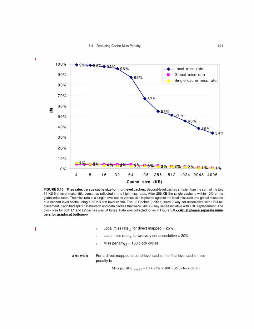
Figures 5.10 and 5.11 show how miss rates and relative execution time changewith the size of a second-level cache for one design. From these figures we cangain two insights. The first is that the global cache miss rate is very similar to thesingle cache miss rate of the second-level cache, provided that the second-levelcache is much larger than the first-level cache. Hence, our intuition and knowl-edge about the first-level caches apply. The second insight is that the local cacherate is not a good measure of secondary caches; it is a function of the miss rate ofthe first-level cache, and hence can vary by changing the first-level cache. Thus,the global cache miss rate should be used when evaluating second-level caches.
With these definitions in place, we can consider the parameters of second-level caches. The foremost difference between the two levels is that the speed ofthe first-level cache affects the clock rate of the CPU, while the speed of thesecond-level cache only affects the miss penalty of the first-level cache. Thus, wecan consider many alternatives in the second-level cache that would be ill chosenfor the first-level cache. There are two major questions for the design of the sec-ond-level cache: Will it lower the average memory access time portion of theCPI, and how much does it cost?
The initial decision is the size of a second-level cache. Since everything in thefirst-level cache is likely to be in the second-level cache, the second-level cacheshould be much bigger than the first. If second-level caches are just a little bigger,the local miss rate will be high. This observation inspires design of huge second-level caches—the size of main memory in older computers! One question iswhether set associativity makes more sense for second-level caches.
E X A M P L E Given the data below, what is the impact of second-level cache as-sociativity on its miss penalty?
n Hit timeL2 for direct mapped = 10 clock cycles
n Two-way set associativity increases hit time by 0.1 clock cycles to 10.1 clock cycles
5.4 Reducing Cache Miss Penalty 401
n Local miss rateL2 for direct mapped = 25%
n Local miss rateL2 for two-way set associative = 20%
n Miss penaltyL2 = 100 clock cycles
A N S W E R For a direct-mapped second-level cache, the first-level cache miss penalty is
Miss penalty1- way L2 = 10 + 25% × 100 = 35.0 clock cycles
FIGURE 5.10 Miss rates versus cache size for multilevel caches. Second-level caches smaller than the sum of the two64-KB first level make little sense, as reflected in the high miss rates. After 256 KB the single cache is within 10% of theglobal miss rates. The miss rate of a single-level cache versus size is plotted against the local miss rate and global miss rateof a second-level cache using a 32-KB first-level cache. The L2 Caches (unified) were 2-way set-associative with LRU re-placement. Each had split L1instruction and data caches that were 64KB 2-way set-associative with LRU replacement. Theblock size for both L1 and L2 caches was 64 bytes. Data was collected for as in Figure 5.6.<<Artist please separate num-bers for graphs at bottom>>
99% 99% 98% 96%
88%
67%
55%51%
46%
39%34%
4 % 4 % 4 % 4 % 4 % 3 % 3 % 2 % 2 % 1 % 1 %6 % 5 % 4 % 3 % 3 % 3 % 2 % 2 % 2 % 1 % 1 %0 %
10%
20%
30%
40%
50%
60%
70%
80%
90%
100%
4 8 1 6 3 2 6 4 128 256 512 1024 2048 4096
Cache size (KB)
Local miss rate
Global miss rate
Single cache miss rate
402 Chapter 5 Memory-Hierarchy Design
Adding the cost of associativity increases the hit cost only 0.1 clock cycles, making the new first-level cache miss penalty
Miss penalty2- way L2 = 10.1 + 20% × 100 = 30.1 clock cycles
In reality, second-level caches are almost always synchronized with the first-level cache and CPU. Accordingly, the second-level hit time must be an integral number of clock cycles. If we are lucky, we shave the second-level hit time to 10 cycles; if not, we round up to 11 cycles. Either choice is an improvement over the direct-mapped second-level cache:
Miss penalty2- way L2 = 10 + 20% × 100 = 30.0 clock cycles
Miss penalty2- way L2 = 11 + 20% × 100 = 31.0 clock cycles
n
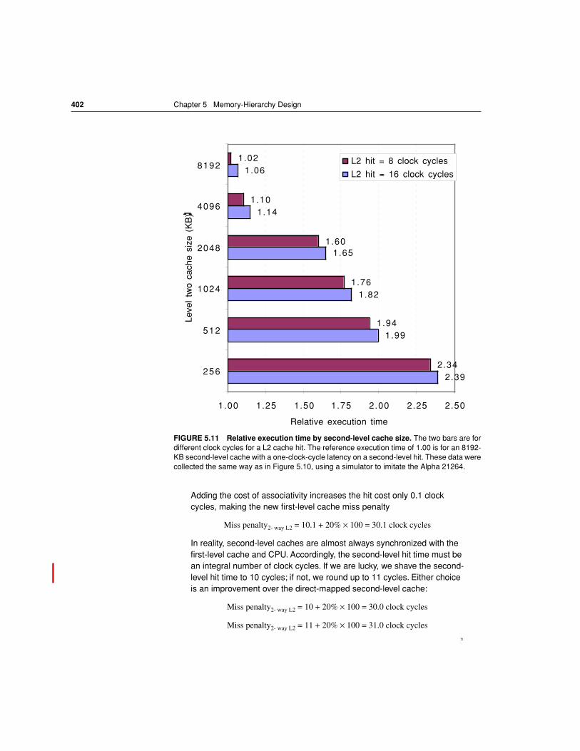
FIGURE 5.11 Relative execution time by second-level cache size. The two bars are fordifferent clock cycles for a L2 cache hit. The reference execution time of 1.00 is for an 8192-KB second-level cache with a one-clock-cycle latency on a second-level hit. These data werecollected the same way as in Figure 5.10, using a simulator to imitate the Alpha 21264.
2.39
1.99
1.82
1.65
1.14
1.06
2.34
1.94
1.76
1.60
1.10
1.02
1.00 1.25 1.50 1.75 2.00 2.25 2.50
256
512
1024
2048
4096
8192
Leve
l tw
o ca
che
size
(K
B)
Relative execution time
L2 hit = 8 clock cycles
L2 hit = 16 clock cycles
5.4 Reducing Cache Miss Penalty 403
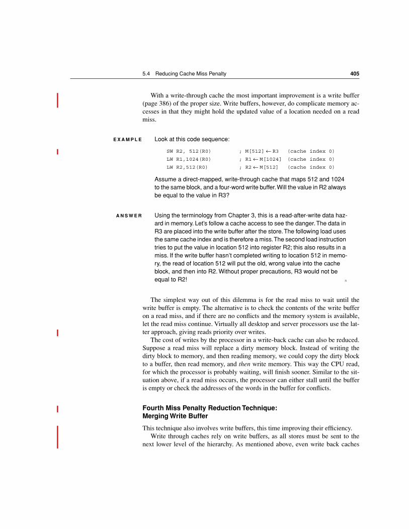
Now we can reduce the miss penalty by reducing the miss rate of the second-lev-el caches.
Another consideration concerns whether data in the first-level cache is in thesecond-level cache. Multilevel inclusion is the natural policy for memory hierar-chies: L1 data is always present in L2. Inclusion is desirable because consistencybetween I/O and caches (or among caches in a multiprocessor) can be determinedjust by checking the second-level cache (see section 8.7).
One drawback to inclusion is that measurements can suggest smaller blocksfor the smaller first-level cache and larger blocks for the larger second-levelcache. For example, the Pentium 4 has 64-byte blocks in its L1 caches and 128-byte blocks in its L2 cache. Inclusion can still be maintained with more work on asecond-level miss. The second-level cache must invalidate all first-level blocksthat map onto the second-level block to be replaced, causing a slightly higherfirst-level miss rate. To avoid such problems, many cache designers keep theblock size the same in all levels of caches.
However, what if the designer can only afford an L2 cache that is slightly big-ger than the L1 cache? Should a significant portion of its space be used as a re-dundant copy of the L1 cache? In such cases a sensible opposite policy ismultilevel exclusion: L1 data is never found in L2 cache. Typically, with exclu-sion a cache miss in L1 results in a swap of blocks between L1 and L2 instead ofa replacement of a L1 block with a L2 block. This policy prevents wasting spacein L2 cache. For example, the AMD Athlon chip obeys the exclusion propertysince it has two 64 KB first level caches and only a 256 KB L2 cache.
As these issues illustrate, although a novice might design the first and second-level caches independently, the designer of the first-level cache has a simpler jobgiven a compatible second-level cache. It is less of a gamble to use a writethrough, for example, if there is a write-back cache at the next level to act as abackstop for repeated writes.
The essence of all cache designs is balancing fast hits and few misses. For sec-ond-level caches, there are many fewer hits than in the first-level cache, so theemphasis shifts to fewer misses. This insight leads to much larger caches andtechniques to lower the miss rate described in section 5.5, such as higher associa-tivity and larger blocks.
Second Miss Penalty Reduction Technique: Critical Word First and Early Restart
Multilevel caches require extra hardware to reduce miss penalty, but not this sec-ond technique. It is based on the observation that the CPU normally needs justone word of the block at a time. This strategy is impatience: Don’t wait for thefull block to be loaded before sending the requested word and restarting the CPU.Here are two specific strategies:
404 Chapter 5 Memory-Hierarchy Design
n Critical word first—Request the missed word first from memory and send it tothe CPU as soon as it arrives; let the CPU continue execution while filling therest of the words in the block. Critical-word-first fetch is also called wrappedfetch and requested word first.
n Early restart—Fetch the words in normal order, but as soon as the requestedword of the block arrives, send it to the CPU and let the CPU continue execu-tion.
Generally these techniques only benefit designs with large cache blocks, sincethe benefit is low unless blocks are large. The problem is that given spatial locali-ty, there is more than random chance that the next miss is to the remainder of theblock. In such cases, the effective miss penalty is the time from the miss until thesecond piece arrives.
E X A M P L E Let’s assume a computer has a 64-byte cache block, an L2 cache that takes 11 clock cycles to get the critical 8 bytes, and then 2 clock cycles per 8 bytes to fetch the rest of the block.(These parameters are similar to the AMD Athlon.) Calculate the average miss penalty for critical word first, assuming that there will be no other accesses to the rest of the block until it is completely fetched. Then calculate assuming the following instruc-tions reads data sequentially 8 bytes at a time from the rest of the block. Compare the times with and without critical word first.
A N S W E R The average miss penalty is 11 clock cycles for critical word first. The Ath-lon can issue two loads per clock cycle, which is faster than the L2 cache can supply data. Thus, it would take 11 + (8-1) x 2 or 25 clock cycles for the CPU to sequentially read a full cache block. Without critical word first, it would take 25 clocks cycle to load the block, and then 8/2 or 4 clocks to issue the loads, giving 29 clock cycles total. n
As this example illustrates, the benefits of critical word first and early restart de-pend on the size of the block and the likelihood of another access to the portionof the block that has not yet been fetched.
The next technique takes overlap between the CPU and cache miss penaltyeven further to reduce the average miss penalty.
Third Miss Penalty Reduction Technique: Giving Priority to Read Misses over Writes
This optimization serves reads before writes have been completed. We start withlooking at complexities of a write buffer.
5.4 Reducing Cache Miss Penalty 405
With a write-through cache the most important improvement is a write buffer(page 386) of the proper size. Write buffers, however, do complicate memory ac-cesses in that they might hold the updated value of a location needed on a readmiss.
E X A M P L E Look at this code sequence:
SW R2, 512(R0) ; M[512] ← R3 (cache index 0)
LW R1,1024(R0) ; R1 ← M[1024] (cache index 0)
LW R2,512(R0) ; R2 ← M[512] (cache index 0)
Assume a direct-mapped, write-through cache that maps 512 and 1024 to the same block, and a four-word write buffer. Will the value in R2 always be equal to the value in R3?
A N S W E R Using the terminology from Chapter 3, this is a read-after-write data haz-ard in memory. Let’s follow a cache access to see the danger. The data in R3 are placed into the write buffer after the store. The following load uses the same cache index and is therefore a miss. The second load instruction tries to put the value in location 512 into register R2; this also results in a miss. If the write buffer hasn’t completed writing to location 512 in memo-ry, the read of location 512 will put the old, wrong value into the cache block, and then into R2. Without proper precautions, R3 would not be equal to R2! n
The simplest way out of this dilemma is for the read miss to wait until thewrite buffer is empty. The alternative is to check the contents of the write bufferon a read miss, and if there are no conflicts and the memory system is available,let the read miss continue. Virtually all desktop and server processors use the lat-ter approach, giving reads priority over writes.
The cost of writes by the processor in a write-back cache can also be reduced.Suppose a read miss will replace a dirty memory block. Instead of writing thedirty block to memory, and then reading memory, we could copy the dirty blockto a buffer, then read memory, and then write memory. This way the CPU read,for which the processor is probably waiting, will finish sooner. Similar to the sit-uation above, if a read miss occurs, the processor can either stall until the bufferis empty or check the addresses of the words in the buffer for conflicts.
Fourth Miss Penalty Reduction Technique: Merging Write Buffer
This technique also involves write buffers, this time improving their efficiency. Write through caches rely on write buffers, as all stores must be sent to the
next lower level of the hierarchy. As mentioned above, even write back caches
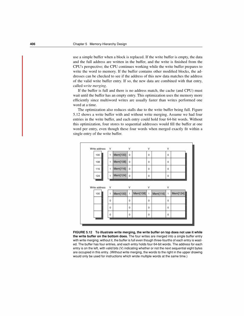
406 Chapter 5 Memory-Hierarchy Design
use a simple buffer when a block is replaced. If the write buffer is empty, the dataand the full address are written in the buffer, and the write is finished from theCPU's perspective; the CPU continues working while the write buffer prepares towrite the word to memory. If the buffer contains other modified blocks, the ad-dresses can be checked to see if the address of this new data matches the addressof the valid write buffer entry. If so, the new data are combined with that entry,called write merging.
If the buffer is full and there is no address match, the cache (and CPU) mustwait until the buffer has an empty entry. This optimization uses the memory moreefficiently since multiword writes are usually faster than writes performed oneword at a time.
The optimization also reduces stalls due to the write buffer being full. Figure5.12 shows a write buffer with and without write merging. Assume we had fourentries in the write buffer, and each entry could hold four 64-bit words. Withoutthis optimization, four stores to sequential addresses would fill the buffer at oneword per entry, even though these four words when merged exactly fit within asingle entry of the write buffer.
FIGURE 5.12 To illustrate write merging, the write buffer on top does not use it whilethe write buffer on the bottom does. The four writes are merged into a single buffer entrywith write merging; without it, the buffer is full even though three-fourths of each entry is wast-ed. The buffer has four entries, and each entry holds four 64-bit words. The address for eachentry is on the left, with valid bits (V) indicating whether or not the next sequential eight bytesare occupied in this entry. (Without write merging, the words to the right in the upper drawingwould only be used for instructions which wrote multiple words at the same time.)
100
108
116
124
Write address
1
1
1
1
V
0
0
0
0
V
0
0
0
0
V
0
0
0
0
V
100
Write address
1
0
0
0
V
1
0
0
0
V
1
0
0
0
V
1
0
0
0
V
Mem[100]
Mem[100]
Mem[108]
Mem[108]
Mem[116]
Mem[116]
Mem[124]
Mem[124]
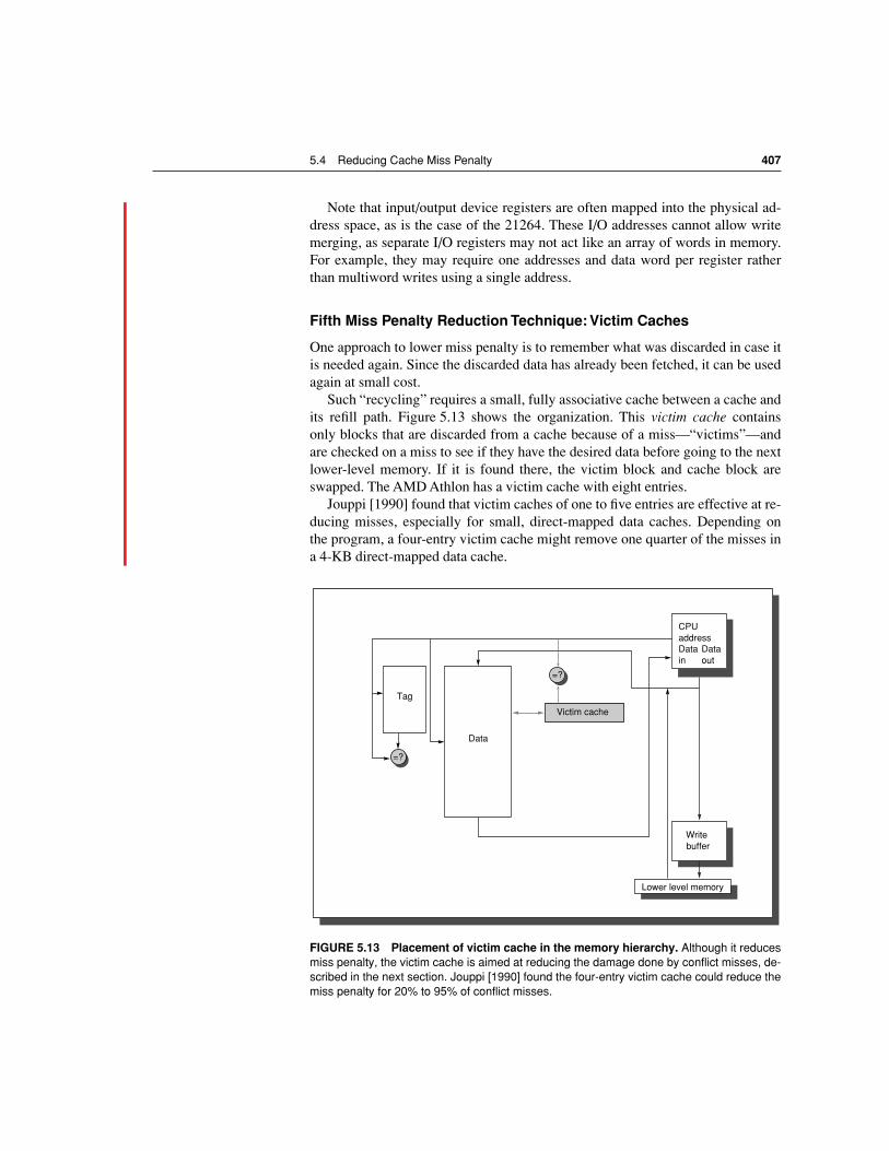
5.4 Reducing Cache Miss Penalty 407
Note that input/output device registers are often mapped into the physical ad-dress space, as is the case of the 21264. These I/O addresses cannot allow writemerging, as separate I/O registers may not act like an array of words in memory.For example, they may require one addresses and data word per register ratherthan multiword writes using a single address.
Fifth Miss Penalty Reduction Technique: Victim Caches
One approach to lower miss penalty is to remember what was discarded in case itis needed again. Since the discarded data has already been fetched, it can be usedagain at small cost.
Such “recycling” requires a small, fully associative cache between a cache andits refill path. Figure 5.13 shows the organization. This victim cache containsonly blocks that are discarded from a cache because of a miss—“victims”—andare checked on a miss to see if they have the desired data before going to the nextlower-level memory. If it is found there, the victim block and cache block areswapped. The AMD Athlon has a victim cache with eight entries.
Jouppi [1990] found that victim caches of one to five entries are effective at re-ducing misses, especially for small, direct-mapped data caches. Depending onthe program, a four-entry victim cache might remove one quarter of the misses ina 4-KB direct-mapped data cache.
FIGURE 5.13 Placement of victim cache in the memory hierarchy. Although it reducesmiss penalty, the victim cache is aimed at reducing the damage done by conflict misses, de-scribed in the next section. Jouppi [1990] found the four-entry victim cache could reduce themiss penalty for 20% to 95% of conflict misses.
CPUaddressDatain
Data out
Write buffer
Lower level memory
Tag
Data
Victim cache
=?
=?
408 Chapter 5 Memory-Hierarchy Design
Summary of Miss Penalty Reduction Techniques
The processor-memory performance gap of Figure 5.2 on page 375 determinesthe miss penalty, and as the gap grows so do techniques that try to close it. Wepresent five in this section. The first technique follows the proverb “the more themerrier”: assuming the principle of locality will keep applying recursively, justkeep adding more levels of increasingly larger caches until you are happy. Thesecond technique is impatience: it retrieves the word of the block that caused themiss rather than waiting for the full block to arrive. The next technique is prefer-ence. It gives priority to reads over writes since the processor generally waits forreads but continues after launching writes. The fourth technique is companion-ship, combining writes to sequential words into a single block to create a moreefficient transfer to memory. Finally comes a cache equivalent of recycling, as avictim cache keeps a few discarded blocks available for when the fickle primarycache wants a word that it recently discarded. All these techniques help with misspenalty, but multilevel caches is probably the most important.
Testimony of the importance of miss penalty is that most desktop and servercomputers use the first four of optimizations. Yet most cache research has con-centrated on reducing the miss rate, so that is where we go in the next section.
The classical approach to improving cache behavior is to reduce miss rates, andwe present five techniques to do so. To gain better insights into the causes ofmisses, we first start with a model that sorts all misses into three simple catego-ries:
n Compulsory—The very first access to a block cannot be in the cache, so theblock must be brought into the cache. These are also called cold start misses orfirst reference misses.
n Capacity—If the cache cannot contain all the blocks needed during executionof a program, capacity misses (in addition to compulsory misses) will occur be-cause of blocks being discarded and later retrieved.
n Conflict—If the block placement strategy is set associative or direct mapped,conflict misses (in addition to compulsory and capacity misses) will occur be-cause a block may be discarded and later retrieved if too many blocks map toits set. These misses are also called collision misses or interference misses. Theidea is that hits in a fully associative cache which become misses in an N-wayset associative cache are due to more than N requests on some popular sets.
Figure 5.14 shows the relative frequency of cache misses, broken down bythe “three C’s.” Compulsory misses are those that occur in an infinite cache. Ca-pacity misses are those that occur in a fully associative cache. Conflict misses arethose that occur going from fully associative to 8-way associative, 4-way associa-tive, and so on. Figure 5.15 presents the same data graphically. The top graph
5.5 Reducing Miss Rate
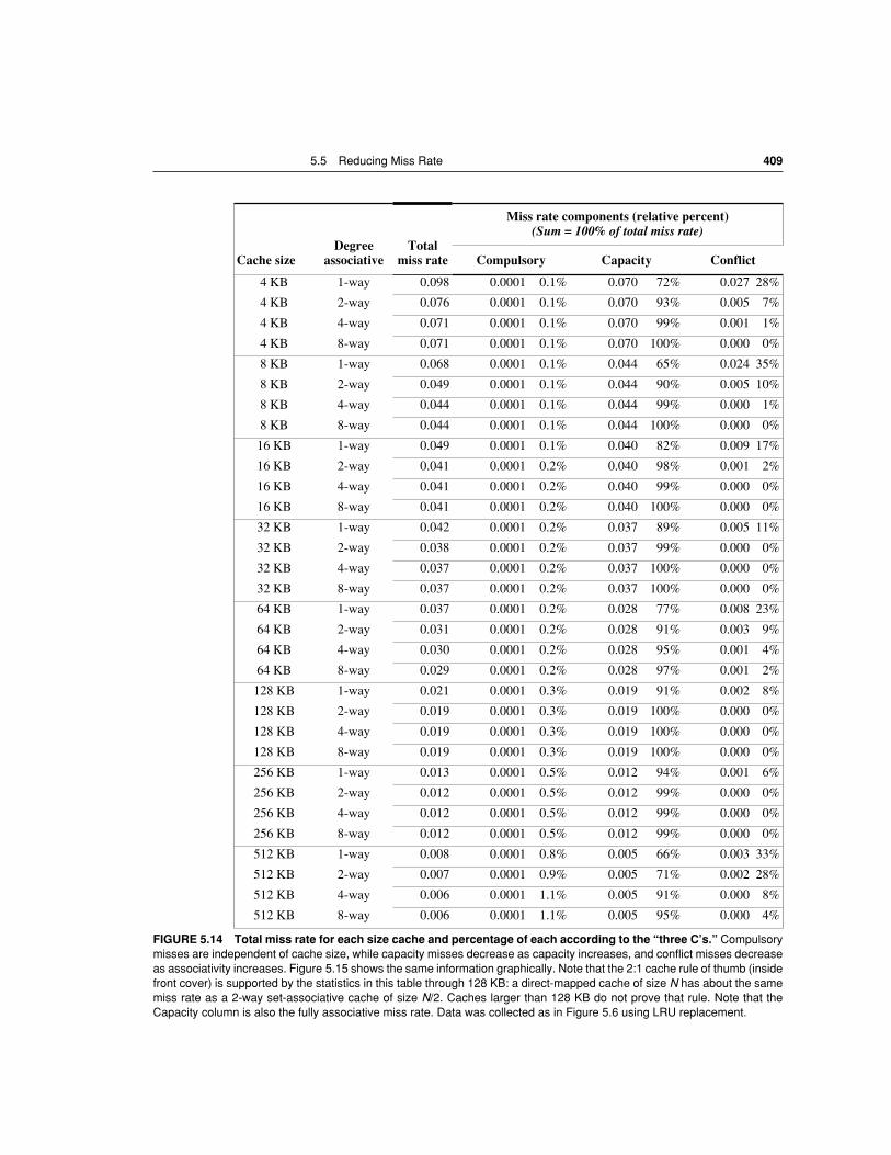
5.5 Reducing Miss Rate 409
Cache sizeDegree
associativeTotal
miss rate
Miss rate components (relative percent) (Sum = 100% of total miss rate)
Compulsory Capacity Conflict
4 KB 1-way 0.098 0.0001 0.1% 0.070 72% 0.027 28%
4 KB 2-way 0.076 0.0001 0.1% 0.070 93% 0.005 7%
4 KB 4-way 0.071 0.0001 0.1% 0.070 99% 0.001 1%
4 KB 8-way 0.071 0.0001 0.1% 0.070 100% 0.000 0%
8 KB 1-way 0.068 0.0001 0.1% 0.044 65% 0.024 35%
8 KB 2-way 0.049 0.0001 0.1% 0.044 90% 0.005 10%
8 KB 4-way 0.044 0.0001 0.1% 0.044 99% 0.000 1%
8 KB 8-way 0.044 0.0001 0.1% 0.044 100% 0.000 0%
16 KB 1-way 0.049 0.0001 0.1% 0.040 82% 0.009 17%
16 KB 2-way 0.041 0.0001 0.2% 0.040 98% 0.001 2%
16 KB 4-way 0.041 0.0001 0.2% 0.040 99% 0.000 0%
16 KB 8-way 0.041 0.0001 0.2% 0.040 100% 0.000 0%
32 KB 1-way 0.042 0.0001 0.2% 0.037 89% 0.005 11%
32 KB 2-way 0.038 0.0001 0.2% 0.037 99% 0.000 0%
32 KB 4-way 0.037 0.0001 0.2% 0.037 100% 0.000 0%
32 KB 8-way 0.037 0.0001 0.2% 0.037 100% 0.000 0%
64 KB 1-way 0.037 0.0001 0.2% 0.028 77% 0.008 23%
64 KB 2-way 0.031 0.0001 0.2% 0.028 91% 0.003 9%
64 KB 4-way 0.030 0.0001 0.2% 0.028 95% 0.001 4%
64 KB 8-way 0.029 0.0001 0.2% 0.028 97% 0.001 2%
128 KB 1-way 0.021 0.0001 0.3% 0.019 91% 0.002 8%
128 KB 2-way 0.019 0.0001 0.3% 0.019 100% 0.000 0%
128 KB 4-way 0.019 0.0001 0.3% 0.019 100% 0.000 0%
128 KB 8-way 0.019 0.0001 0.3% 0.019 100% 0.000 0%
256 KB 1-way 0.013 0.0001 0.5% 0.012 94% 0.001 6%
256 KB 2-way 0.012 0.0001 0.5% 0.012 99% 0.000 0%
256 KB 4-way 0.012 0.0001 0.5% 0.012 99% 0.000 0%
256 KB 8-way 0.012 0.0001 0.5% 0.012 99% 0.000 0%
512 KB 1-way 0.008 0.0001 0.8% 0.005 66% 0.003 33%
512 KB 2-way 0.007 0.0001 0.9% 0.005 71% 0.002 28%
512 KB 4-way 0.006 0.0001 1.1% 0.005 91% 0.000 8%
512 KB 8-way 0.006 0.0001 1.1% 0.005 95% 0.000 4%
FIGURE 5.14 Total miss rate for each size cache and percentage of each according to the “three C’s.” Compulsorymisses are independent of cache size, while capacity misses decrease as capacity increases, and conflict misses decreaseas associativity increases. Figure 5.15 shows the same information graphically. Note that the 2:1 cache rule of thumb (insidefront cover) is supported by the statistics in this table through 128 KB: a direct-mapped cache of size N has about the samemiss rate as a 2-way set-associative cache of size N/2. Caches larger than 128 KB do not prove that rule. Note that theCapacity column is also the fully associative miss rate. Data was collected as in Figure 5.6 using LRU replacement.
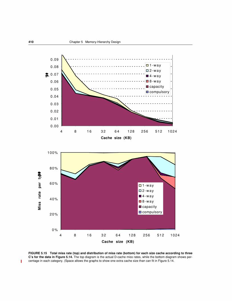
410 Chapter 5 Memory-Hierarchy Design
FIGURE 5.15 Total miss rate (top) and distribution of miss rate (bottom) for each size cache according to threeC’s for the data in Figure 5.14. The top diagram is the actual D-cache miss rates, while the bottom diagram shows per-centage in each category. (Space allows the graphs to show one extra cache size than can fit in Figure 5.14.
0 %
20%
40%
60%
80%
100%
4 8 1 6 3 2 6 4 128 256 512 1024
Cache size (KB)
Mis
s
rate
p
er
typ
e
1 -way
2 -way
4 -way
8 -way
capacity
compulsory
0.00
0.01
0.02
0.03
0.04
0.05
0.06
0.07
0.08
0.09
4 8 1 6 3 2 6 4 128 256 512 1024
Cache size (KB)
1 -way
2 -way
4 -way
8 -way
capacity
compulsory
5.5 Reducing Miss Rate 411
shows absolute miss rates; the bottom graph plots percentage of all the misses bytype of miss as a function of cache size.
To show the benefit of associativity, conflict misses are divided into missescaused by each decrease in associativity. Here are the four divisions of conflictmisses and how they are calculated:
n Eight-way—conflict misses due to going from fully associative (no conflicts)to eight-way associative
n Four-way—conflict misses due to going from eight-way associative to four-way associative
n Two-way—conflict misses due to going from four-way associative to two-wayassociative
n One-way—conflict misses due to going from two-way associative to one-wayassociative (direct mapped)
As we can see from the figures, the compulsory miss rate of the SPEC2000 pro-grams is very small, as it is for many long-running programs.
Having identified the three C’s, what can a computer designer do about them?Conceptually, conflicts are the easiest: Fully associative placement avoids allconflict misses. Full associativity is expensive in hardware, however, and mayslow the processor clock rate (see the example above), leading to lower overallperformance.
There is little to be done about capacity except to enlarge the cache. If theupper-level memory is much smaller than what is needed for a program, and asignificant percentage of the time is spent moving data between two levels in thehierarchy, the memory hierarchy is said to thrash. Because so many replacementsare required, thrashing means the computer runs close to the speed of the lower-level memory, or maybe even slower because of the miss overhead.
Another approach to improving the three C’s is to make blocks larger to re-duce the number of compulsory misses, but, as we shall see, large blocks can in-crease other kinds of misses.
The three C’s give insight into the cause of misses, but this simple model hasits limits; it gives you insight into average behavior but may not explain an indi-vidual miss. For example, changing cache size changes conflict misses as well ascapacity misses, since a larger cache spreads out references to more blocks. Thus,a miss might move from a capacity miss to a conflict miss as cache size changes.Note that the three C’s also ignore replacement policy, since it is difficult tomodel and since, in general, it is less significant. In specific circumstances the re-placement policy can actually lead to anomalous behavior, such as poorer missrates for larger associativity, which contradicts the three C’s model. (Some haveproposed using an address trace to determine optimal placement to avoid place-ment misses from the 3 Cs model; we’ve not followed that advice here.)
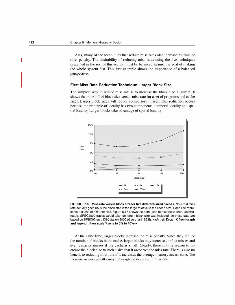
412 Chapter 5 Memory-Hierarchy Design
Alas, many of the techniques that reduce miss rates also increase hit time ormiss penalty. The desirability of reducing miss rates using the five techniquespresented in the rest of this section must be balanced against the goal of makingthe whole system fast. This first example shows the importance of a balancedperspective.
First Miss Rate Reduction Technique: Larger Block Size
The simplest way to reduce miss rate is to increase the block size. Figure 5.16shows the trade-off of block size versus miss rate for a set of programs and cachesizes. Larger block sizes will reduce compulsory misses. This reduction occursbecause the principle of locality has two components: temporal locality and spa-tial locality. Larger blocks take advantage of spatial locality.
At the same time, larger blocks increase the miss penalty. Since they reducethe number of blocks in the cache, larger blocks may increase conflict misses andeven capacity misses if the cache is small. Clearly, there is little reason to in-crease the block size to such a size that it increases the miss rate. There is also nobenefit to reducing miss rate if it increases the average memory access time. Theincrease in miss penalty may outweigh the decrease in miss rate.
FIGURE 5.16 Miss rate versus block size for five different-sized caches. Note that missrate actually goes up is the block size is too large relative to the cache size. Each line repre-sents a cache of different size. Figure 5.17 shows the data used to plot these lines. Unfortu-nately, SPEC2000 traces would take too long if block size was included, so these data arebased on SPEC92 on a DECstation 5000 (Gee et al [1993]). <<Artist: Drop 1K from graphand legend.; then scale Y axis to 0% to 10%>>
5%
16
Block size
32
10%
15%
20%
25%
64 128 256
Missrate
0%
1k 4k 16k
64k 256k
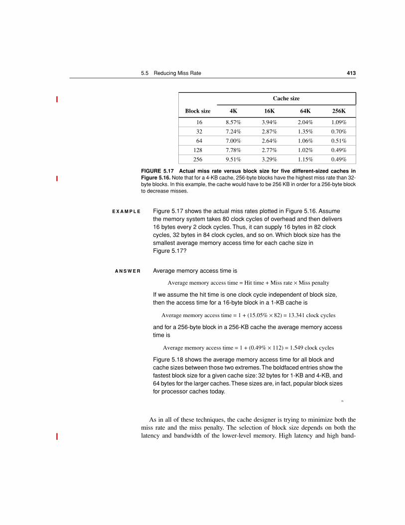
5.5 Reducing Miss Rate 413
E X A M P L E Figure 5.17 shows the actual miss rates plotted in Figure 5.16. Assume the memory system takes 80 clock cycles of overhead and then delivers 16 bytes every 2 clock cycles. Thus, it can supply 16 bytes in 82 clock cycles, 32 bytes in 84 clock cycles, and so on. Which block size has the smallest average memory access time for each cache size in Figure 5.17?
A N S W E R Average memory access time is
Average memory access time = Hit time + Miss rate × Miss penalty
If we assume the hit time is one clock cycle independent of block size, then the access time for a 16-byte block in a 1-KB cache is
Average memory access time = 1 + (15.05% × 82) = 13.341 clock cycles
and for a 256-byte block in a 256-KB cache the average memory access time is
Average memory access time = 1 + (0.49% × 112) = 1.549 clock cycles
Figure 5.18 shows the average memory access time for all block and cache sizes between those two extremes. The boldfaced entries show the fastest block size for a given cache size: 32 bytes for 1-KB and 4-KB, and 64 bytes for the larger caches. These sizes are, in fact, popular block sizes for processor caches today.
n
As in all of these techniques, the cache designer is trying to minimize both themiss rate and the miss penalty. The selection of block size depends on both thelatency and bandwidth of the lower-level memory. High latency and high band-
Cache size
Block size 4K 16K 64K 256K
16 8.57% 3.94% 2.04% 1.09%
32 7.24% 2.87% 1.35% 0.70%
64 7.00% 2.64% 1.06% 0.51%
128 7.78% 2.77% 1.02% 0.49%
256 9.51% 3.29% 1.15% 0.49%
FIGURE 5.17 Actual miss rate versus block size for five different-sized caches inFigure 5.16. Note that for a 4-KB cache, 256-byte blocks have the highest miss rate than 32-byte blocks. In this example, the cache would have to be 256 KB in order for a 256-byte blockto decrease misses.
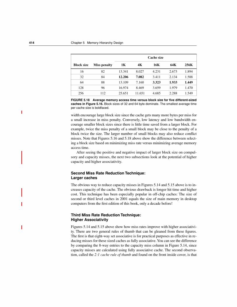
414 Chapter 5 Memory-Hierarchy Design
width encourage large block size since the cache gets many more bytes per miss fora small increase in miss penalty. Conversely, low latency and low bandwidth en-courage smaller block sizes since there is little time saved from a larger block. Forexample, twice the miss penalty of a small block may be close to the penalty of ablock twice the size. The larger number of small blocks may also reduce conflictmisses. Note that Figures 5.16 and 5.18 above show the difference between select-ing a block size based on minimizing miss rate versus minimizing average memoryaccess time.
After seeing the positive and negative impact of larger block size on compul-sory and capacity misses, the next two subsections look at the potential of highercapacity and higher associativity.
Second Miss Rate Reduction Technique: Larger caches
The obvious way to reduce capacity misses in Figures 5.14 and 5.15 above is to in-creases capacity of the cache. The obvious drawback is longer hit time and highercost. This technique has been especially popular in off-chip caches: The size ofsecond or third level caches in 2001 equals the size of main memory in desktopcomputers from the first edition of this book, only a decade before!
Third Miss Rate Reduction Technique: Higher Associativity
Figures 5.14 and 5.15 above show how miss rates improve with higher associativi-ty. There are two general rules of thumb that can be gleaned from these figures.The first is that eight-way set associative is for practical purposes as effective in re-ducing misses for these sized caches as fully associative. You can see the differenceby comparing the 8-way entries to the capacity miss column in Figure 5.14, sincecapacity misses are calculated using fully associative cache. The second observa-tion, called the 2:1 cache rule of thumb and found on the front inside cover, is that
Cache size
Block size Miss penalty 1K 4K 16K 64K 256K
16 82 13.341 8.027 4.231 2.673 1.894
32 84 12.206 7.082 3.411 2.134 1.588
64 88 13.109 7.160 3.323 1.933 1.449
128 96 16.974 8.469 3.659 1.979 1.470
256 112 25.651 11.651 4.685 2.288 1.549
FIGURE 5.18 Average memory access time versus block size for five different-sizedcaches in Figure 5.16. Block sizes of 32 and 64 byte dominate. The smallest average timeper cache size is boldfaced.
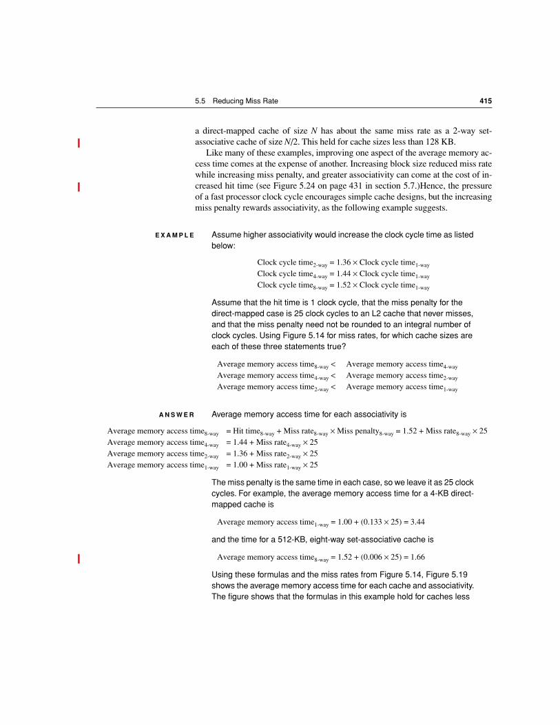
5.5 Reducing Miss Rate 415
a direct-mapped cache of size N has about the same miss rate as a 2-way set-associative cache of size N/2. This held for cache sizes less than 128 KB.
Like many of these examples, improving one aspect of the average memory ac-cess time comes at the expense of another. Increasing block size reduced miss ratewhile increasing miss penalty, and greater associativity can come at the cost of in-creased hit time (see Figure 5.24 on page 431 in section 5.7.)Hence, the pressureof a fast processor clock cycle encourages simple cache designs, but the increasingmiss penalty rewards associativity, as the following example suggests.
E X A M P L E Assume higher associativity would increase the clock cycle time as listed below:
Clock cycle time2-way = 1.36 × Clock cycle time1-way
Clock cycle time4-way = 1.44 × Clock cycle time1-way
Clock cycle time8-way = 1.52 × Clock cycle time1-way
Assume that the hit time is 1 clock cycle, that the miss penalty for the direct-mapped case is 25 clock cycles to an L2 cache that never misses, and that the miss penalty need not be rounded to an integral number of clock cycles. Using Figure 5.14 for miss rates, for which cache sizes are each of these three statements true?
Average memory access time8-way < Average memory access time4-way
Average memory access time4-way < Average memory access time2-way
Average memory access time2-way < Average memory access time1-way
A N S W E R Average memory access time for each associativity is
Average memory access time8-way = Hit time8-way + Miss rate8-way × Miss penalty8-way = 1.52 + Miss rate8-way × 25Average memory access time4-way = 1.44 + Miss rate4-way × 25Average memory access time2-way = 1.36 + Miss rate2-way × 25Average memory access time1-way = 1.00 + Miss rate1-way × 25
The miss penalty is the same time in each case, so we leave it as 25 clock cycles. For example, the average memory access time for a 4-KB direct-mapped cache is
Average memory access time1-way = 1.00 + (0.133 × 25) = 3.44
and the time for a 512-KB, eight-way set-associative cache is
Average memory access time8-way = 1.52 + (0.006 × 25) = 1.66
Using these formulas and the miss rates from Figure 5.14, Figure 5.19 shows the average memory access time for each cache and associativity. The figure shows that the formulas in this example hold for caches less
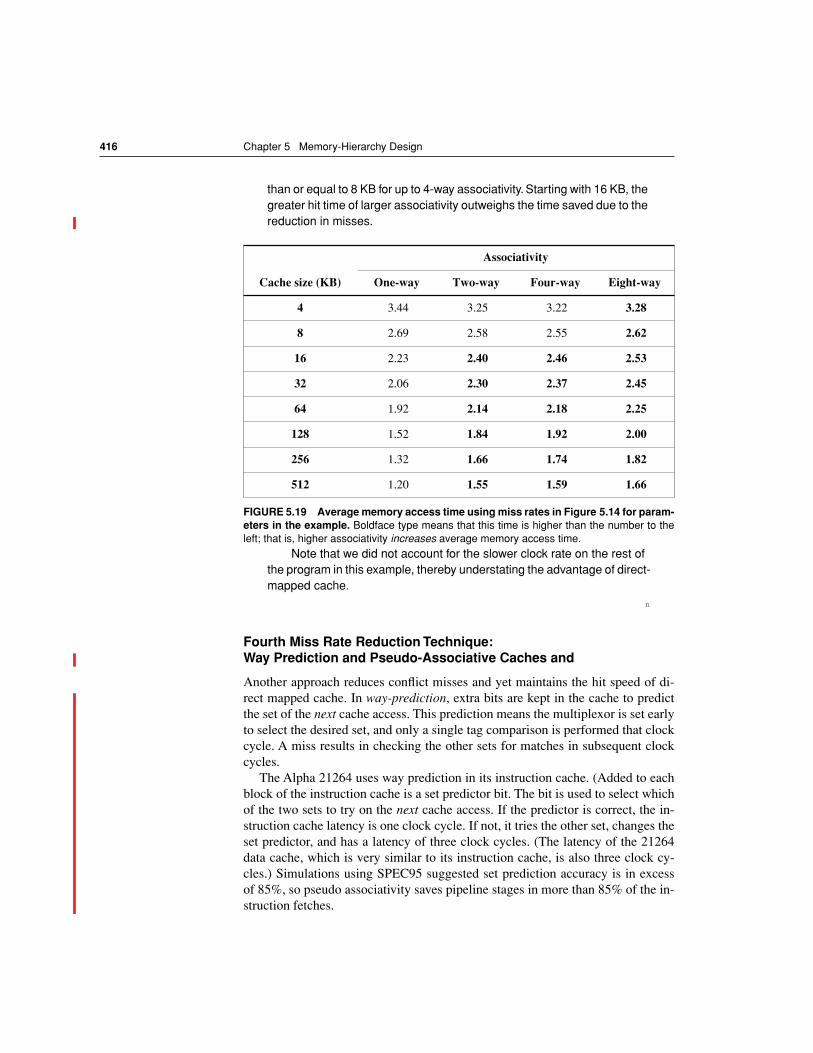
416 Chapter 5 Memory-Hierarchy Design
than or equal to 8 KB for up to 4-way associativity. Starting with 16 KB, the greater hit time of larger associativity outweighs the time saved due to the reduction in misses.
Note that we did not account for the slower clock rate on the rest of the program in this example, thereby understating the advantage of direct-mapped cache.
n
Fourth Miss Rate Reduction Technique: Way Prediction and Pseudo-Associative Caches and
Another approach reduces conflict misses and yet maintains the hit speed of di-rect mapped cache. In way-prediction, extra bits are kept in the cache to predictthe set of the next cache access. This prediction means the multiplexor is set earlyto select the desired set, and only a single tag comparison is performed that clockcycle. A miss results in checking the other sets for matches in subsequent clockcycles.
The Alpha 21264 uses way prediction in its instruction cache. (Added to eachblock of the instruction cache is a set predictor bit. The bit is used to select whichof the two sets to try on the next cache access. If the predictor is correct, the in-struction cache latency is one clock cycle. If not, it tries the other set, changes theset predictor, and has a latency of three clock cycles. (The latency of the 21264data cache, which is very similar to its instruction cache, is also three clock cy-cles.) Simulations using SPEC95 suggested set prediction accuracy is in excessof 85%, so pseudo associativity saves pipeline stages in more than 85% of the in-struction fetches.
Associativity
Cache size (KB) One-way Two-way Four-way Eight-way
4 3.44 3.25 3.22 3.28
8 2.69 2.58 2.55 2.62
16 2.23 2.40 2.46 2.53
32 2.06 2.30 2.37 2.45
64 1.92 2.14 2.18 2.25
128 1.52 1.84 1.92 2.00
256 1.32 1.66 1.74 1.82
512 1.20 1.55 1.59 1.66
FIGURE 5.19 Average memory access time using miss rates in Figure 5.14 for param-eters in the example. Boldface type means that this time is higher than the number to theleft; that is, higher associativity increases average memory access time.
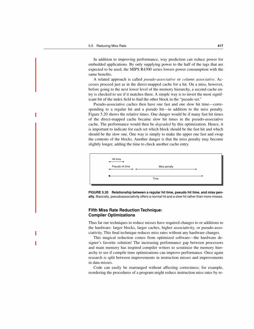
5.5 Reducing Miss Rate 417
In addition to improving performance, way prediction can reduce power forembedded applications. By only supplying power to the half of the tags that areexpected to be used, the MIPS R4300 series lowers power consumption with thesame benefits.
A related approach is called pseudo-associative or column associative. Ac-cesses proceed just as in the direct-mapped cache for a hit. On a miss, however,before going to the next lower level of the memory hierarchy, a second cache en-try is checked to see if it matches there. A simple way is to invert the most signif-icant bit of the index field to find the other block in the “pseudo set.”
Pseudo-associative caches then have one fast and one slow hit time—corre-sponding to a regular hit and a pseudo hit—in addition to the miss penalty.Figure 5.20 shows the relative times. One danger would be if many fast hit timesof the direct-mapped cache became slow hit times in the pseudo-associativecache. The performance would then be degraded by this optimization. Hence, itis important to indicate for each set which block should be the fast hit and whichshould be the slow one. One way is simply to make the upper one fast and swapthe contents of the blocks. Another danger is that the miss penalty may becomeslightly longer, adding the time to check another cache entry.
Fifth Miss Rate Reduction Technique: Compiler Optimizations
Thus far our techniques to reduce misses have required changes to or additions tothe hardware: larger blocks, larger caches, higher associativity, or pseudo-asso-ciativity. This final technique reduces miss rates without any hardware changes.
This magical reduction comes from optimized software—the hardware de-signer’s favorite solution! The increasing performance gap between processorsand main memory has inspired compiler writers to scrutinize the memory hier-archy to see if compile time optimizations can improve performance. Once againresearch is split between improvements in instruction misses and improvementsin data misses.
Code can easily be rearranged without affecting correctness; for example,reordering the procedures of a program might reduce instruction miss rates by re-
FIGURE 5.20 Relationship between a regular hit time, pseudo hit time, and miss pen-alty. Basically, pseudoassociativity offers a normal hit and a slow hit rather than more misses.
Hit time
Pseudo hit time Miss penalty
Time
418 Chapter 5 Memory-Hierarchy Design
ducing conflict misses. McFarling [1989] looked at using profiling information todetermine likely conflicts between groups of instructions. Reordering the instruc-tions reduced misses by 50% for a 2-KB direct-mapped instruction cache with 4-byte blocks, and by 75% in an 8-KB cache. McFarling got the best performancewhen it was possible to prevent some instructions from ever entering the cache.Even without that feature, optimized programs on a direct-mapped cache missedless than unoptimized programs on an eight-way set-associative cache of thesame size.
Another code optimization aims for better efficiency from long cache blocks.Aligning basic blocks so that the entry point is at the beginning of a cache blockdecreases the chance of a cache miss for sequential code. Data have even fewer restrictions on location than code. The goal of suchtransformations is to try to improve the spatial and temporal locality of the data.For example, array calculations can be changed to operate on all the data in acache block rather than blindly striding through arrays in the order the program-mer happened to place the loop.
To give a feeling of this type of optimization, we will show two examples,transforming the C code by hand to reduce cache misses.
Loop InterchangeSome programs have nested loops that access data in memory in nonsequentialorder. Simply exchanging the nesting of the loops can make the code access thedata in the order it is stored. Assuming the arrays do not fit in cache, this tech-nique reduces misses by improving spatial locality; reordering maximizes use ofdata in a cache block before it is discarded.
/* Before */
for (j = 0; j < 100; j = j+1)
for (i = 0; i < 5000; i = i+1)
x[i][j] = 2 * x[i][j];
/* After */
for (i = 0; i < 5000; i = i+1)
for (j = 0; j < 100; j = j+1)
x[i][j] = 2 * x[i][j];
The original code would skip through memory in strides of 100 words, while therevised version accesses all the words in one cache block before going to the nextblock. This optimization improves cache performance without affecting the num-ber of instructions executed, unlike the prior example.
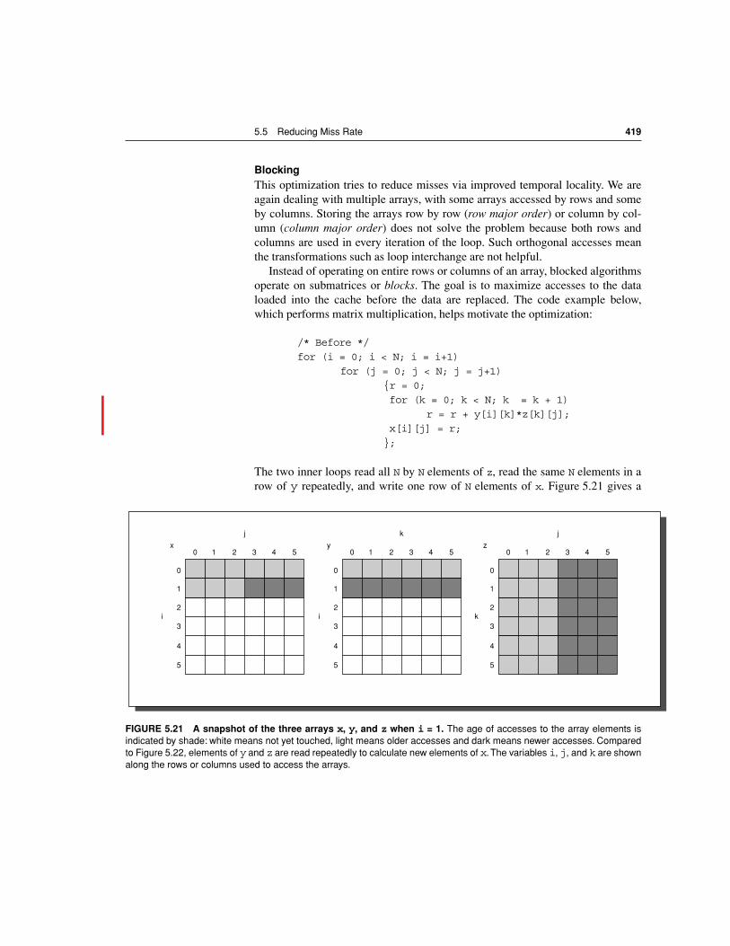
5.5 Reducing Miss Rate 419
BlockingThis optimization tries to reduce misses via improved temporal locality. We areagain dealing with multiple arrays, with some arrays accessed by rows and someby columns. Storing the arrays row by row (row major order) or column by col-umn (column major order) does not solve the problem because both rows andcolumns are used in every iteration of the loop. Such orthogonal accesses meanthe transformations such as loop interchange are not helpful.
Instead of operating on entire rows or columns of an array, blocked algorithmsoperate on submatrices or blocks. The goal is to maximize accesses to the dataloaded into the cache before the data are replaced. The code example below,which performs matrix multiplication, helps motivate the optimization:
/* Before */
for (i = 0; i < N; i = i+1)
for (j = 0; j < N; j = j+1)
{r = 0;
for (k = 0; k < N; k = k + 1)
r = r + y[i][k]*z[k][j];
x[i][j] = r;
};
The two inner loops read all N by N elements of z, read the same N elements in arow of y repeatedly, and write one row of N elements of x. Figure 5.21 gives a
FIGURE 5.21 A snapshot of the three arrays x, y, and z when i = 1. The age of accesses to the array elements isindicated by shade: white means not yet touched, light means older accesses and dark means newer accesses. Comparedto Figure 5.22, elements of y and z are read repeatedly to calculate new elements of x. The variables i, j, and k are shownalong the rows or columns used to access the arrays.
0
1
2
3
4
5
10 2 3 4 5x
j
i
0
1
2
3
4
5
10 2 3 4 5y
k
i
0
1
2
3
4
5
10 2 3 4 5z
j
k
420 Chapter 5 Memory-Hierarchy Design
snapshot of the accesses to the three arrays. A dark shade indicates a recent ac-cess, a light shade indicates an older access, and white means not yet accessed.
The number of capacity misses clearly depends on N and the size of the cache.If it can hold all three N by N matrices, then all is well, provided there are nocache conflicts. If the cache can hold one N by N matrix and one row of N, then atleast the i-th row of y and the array z may stay in the cache. Less than that andmisses may occur for both x and z. In the worst case, there would be 2N3 + N2
memory words accessed for N3 operations. To ensure that the elements being accessed can fit in the cache, the original
code is changed to compute on a submatrix of size B by B. Two inner loops nowcompute in steps of size B rather than the full length of x and z. B is called theblocking factor. (Assume x is initialized to zero.)
/* After */
for (jj = 0; jj < N; jj = jj+B)
for (kk = 0; kk < N; kk = kk+B)
for (i = 0; i < N; i = i+1)
for (j = jj; j < min(jj+B,N); j = j+1)
{r = 0;
for (k = kk; k < min(kk+B,N); k = k + 1)
r = r + y[i][k]*z[k][j];
x[i][j] = x[i][j] + r;
};
Figure 5.22 illustrates the accesses to the three arrays using blocking. Looking onlyat capacity misses, the total number of memory words accessed is 2N3/B + N2. Thistotal is an improvement by about a factor of B. Hence, blocking exploits a combi-nation of spatial and temporal locality, since y benefits from spatial locality and zbenefits from temporal locality.
Although we have aimed at reducing cache misses, blocking can also be usedto help register allocation. By taking a small blocking size such that the block canbe held in registers, we can minimize the number of loads and stores in theprogram.
Summary of Reducing Cache Miss Rate
This section first presented the three C’s model of cache misses: compulsory, ca-pacity, and conflict. This intuitive model led to three obvious optimizations: larg-er block size to reduce compulsory misses, larger cache size to reduce capacitymisses, and higher associativity to reduce conflict misses. Since higher associa-tivity may affect cache hit time or cache power consumption, way predictionchecks only a piece of the cache for hits and then on a miss checks the rest. Thefinal technique is the favorite of the hardware designer, leaving cache optimiza-tions to the compiler.
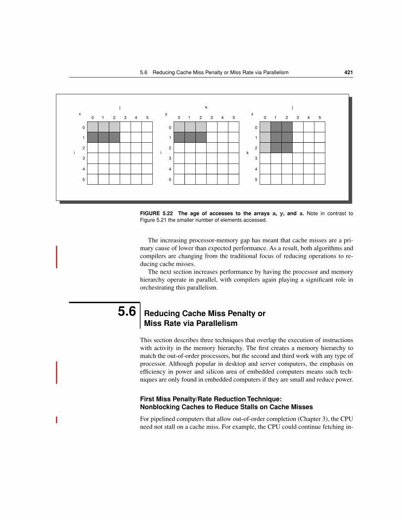
5.6 Reducing Cache Miss Penalty or Miss Rate via Parallelism 421
The increasing processor-memory gap has meant that cache misses are a pri-mary cause of lower than expected performance. As a result, both algorithms andcompilers are changing from the traditional focus of reducing operations to re-ducing cache misses.
The next section increases performance by having the processor and memoryhierarchy operate in parallel, with compilers again playing a significant role inorchestrating this parallelism.
This section describes three techniques that overlap the execution of instructionswith activity in the memory hierarchy. The first creates a memory hierarchy tomatch the out-of-order processors, but the second and third work with any type ofprocessor. Although popular in desktop and server computers, the emphasis onefficiency in power and silicon area of embedded computers means such tech-niques are only found in embedded computers if they are small and reduce power.
First Miss Penalty/Rate Reduction Technique: Nonblocking Caches to Reduce Stalls on Cache Misses
For pipelined computers that allow out-of-order completion (Chapter 3), the CPUneed not stall on a cache miss. For example, the CPU could continue fetching in-
FIGURE 5.22 The age of accesses to the arrays x, y, and z. Note in contrast toFigure 5.21 the smaller number of elements accessed.
5.6 Reducing Cache Miss Penalty or Miss Rate via Parallelism
0
1
2
3
4
5
10 2 3 4 5x
j
i
0
1
2
3
4
5
10 2 3 4 5y
k
i
0
1
2
3
4
5
10 2 3 4 5z
j
k
422 Chapter 5 Memory-Hierarchy Design
structions from the instruction cache while waiting for the data cache to returnthe missing data. A nonblocking cache or lockup-free cache escalates the poten-tial benefits of such a scheme by allowing the data cache to continue to supplycache hits during a miss. This “hit under miss” optimization reduces the effectivemiss penalty by being helpful during a miss instead of ignoring the requests ofthe CPU. A subtle and complex option is that the cache may further lower the ef-fective miss penalty if it can overlap multiple misses: a “hit under multiple miss”or “miss under miss” optimization. The second option is beneficial only if thememory system can service multiple misses (see page 441). Be aware that hit un-der miss significantly increases the complexity of the cache controller as therecan be multiple outstanding memory accesses.
Figure 5.23 shows the average time in clock cycles for cache misses for an8-KB data cache as the number of outstanding misses is varied. Floating-pointprograms benefit from increasing complexity, while integer programs get al-most all of the benefit from a simple hit-under-one-miss scheme. Following thediscussion in Chapter 3, the number of simultaneous outstanding misses limitsachievable instruction level parallelism in programs.
E X A M P L E For the cache described in Figure 5.23, which is more important for floating-point programs: two-way set associativity or hit under one miss? What about integer programs? Assume the following average miss rates for 8-KB data caches: 11.4% for floating-point programs with a direct-mapped cache, 10.7% for these programs with a two-way set-associative cache, 7.4% for integer programs with a direct-mapped cache, and 6.0% for integer programs with a two-way set-associative cache. Assume the average memory stall time is just the product of the miss rate and the miss penalty.
A N S W E R The numbers for Figure 5.23 were based on a miss penalty of 16 clock cy-cles assuming an L2 cache. Although this is low for a miss penalty (we’ll see how in the next subsection), let’s stick with it for consistency. For float-ing-point programs the average memory stall times are
Miss rateDM × Miss penalty = 11.4% × 16 = 1.84
Miss rate2-way × Miss penalty = 10.7% × 16 = 1.71
The memory stalls of two-way are thus 1.71/1.84 or 93% of direct-mapped cache. The caption of Figure 5.23 says hit under one miss reduces the average memory stall time to 76% of a blocking cache. Hence, for floating-point programs, the direct-mapped data cache sup-porting hit under one miss gives better performance than a two-way set-associative cache that blocks on a miss.
For integer programs the calculation is
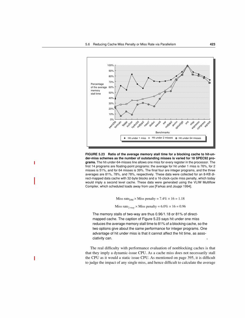
5.6 Reducing Cache Miss Penalty or Miss Rate via Parallelism 423
Miss rateDM × Miss penalty = 7.4% × 16 = 1.18
Miss rate2-way × Miss penalty = 6.0% × 16 = 0.96
The memory stalls of two-way are thus 0.96/1.18 or 81% of direct-mapped cache. The caption of Figure 5.23 says hit under one miss reduces the average memory stall time to 81% of a blocking cache, so the two options give about the same performance for integer programs. One advantage of hit under miss is that it cannot affect the hit time, as asso-ciativity can. n
The real difficulty with performance evaluation of nonblocking caches is thatthat they imply a dynamic-issue CPU. As a cache miss does not necessarily stallthe CPU as it would a static issue CPU. As mentioned on page 395, it is difficultto judge the impact of any single miss, and hence difficult to calculate the average
FIGURE 5.23 Ratio of the average memory stall time for a blocking cache to hit-un-der-miss schemes as the number of outstanding misses is varied for 18 SPEC92 pro-grams. The hit-under-64-misses line allows one miss for every register in the processor. Thefirst 14 programs are floating-point programs: the average for hit under 1 miss is 76%, for 2misses is 51%, and for 64 misses is 39%. The final four are integer programs, and the threeaverages are 81%, 78%, and 78%, respectively. These data were collected for an 8-KB di-rect-mapped data cache with 32-byte blocks and a 16-clock-cycle miss penalty, which todaywould imply a second level cache. These data were generated using the VLIW MultiflowCompiler, which scheduled loads away from use [Farkas and Jouppi 1994].
100%
0%
10%
20%
30%
40%
50%
60%
70%
80%
90%
Percentage of the averagememorystall time
Benchmarks
swm
256
fppp
p
hydr
o2d
nasa
7
wave5
mdlj
dp2
spice
2g6
xlisp
com
pres
s
tom
catv
su2c
or
mdlj
sp2
dodu
cea
r
alvinn or
a
espr
esso
eqnt
ott
Hit under 1 miss Hit under 2 misses Hit under 64 misses
424 Chapter 5 Memory-Hierarchy Design
memory access time. As was the case of a second miss to the remaining blockwith critical word first above, the effective miss penalty is not the sum of themisses but the non-overlapped time that the CPU is stalled. In general, out-of-or-der CPUs are capable of hiding the miss penalty of an L1 data cache miss whichhits in the L2 cache, but not capable of hiding a significant fraction of an L2cache miss. Changing the program to pipeline L2 misses can help, especially to abanked memory system (see section 5.8).
Chapter 1 discusses the pros and cons of execution-driven simulation versustrace-driven simulation. Cache studies involving an out-of-order CPUs use exe-cution-driven simulation to evaluate innovations, as avoiding a cache miss that iscompletely hidden by dynamic issue does not help performance.
An added complexity of multiple outstanding misses is that it is now possiblefor there to be more than one miss request to the same block. For example, with64 byte blocks there could be a miss to address 1000 and then later a miss to ad-dress 1032. Thus, the hardware must check on misses to be sure it is not to blockalready being requested to avoid possible incoherency problems and to save time.
Second Miss Penalty/Rate Reduction Technique:Hardware Prefetching of Instructions and Data
Nonblocking caches effectively reduce the miss penalty by overlapping executionwith memory access. To have value, we need a processor that can allow instruc-tions to execute out-of-order. Another approach is to prefetch items before theyare requested by the processor. Both instructions and data can be prefetched,either directly into the caches or into an external buffer that can be more quicklyaccessed than main memory.
Instruction prefetch is frequently done in hardware outside of the cache. Typi-cally, the processor fetches two blocks on a miss: the requested block and thenext consecutive block. The requested block is placed in the instruction cachewhen it returns, and the prefetched block is placed into the instruction streambuffer. If the requested block is present in the instruction stream buffer, the origi-nal cache request is canceled, the block is read from the stream buffer, and thenext prefetch request is issued.
Jouppi [1990] found that a single instruction stream buffer would catch 15%to 25% of the misses from a 4-KB direct-mapped instruction cache with 16-byteblocks. With 4 blocks in the instruction stream buffer the hit rate improves toabout 50%, and with 16 blocks to 72%.
A similar approach can be applied to data accesses. Jouppi found that a singledata stream buffer caught about 25% of the misses from the 4-KB direct-mappedcache. Instead of having a single stream, there could be multiple stream buffersbeyond the data cache, each prefetching at different addresses. Jouppi found thatfour data stream buffers increased the data hit rate to 43%. Palacharla and Kessler[1994] looked at a set of scientific programs and considered stream buffers thatcould handle either instructions or data. They found that eight stream bufferscould capture 50% to 70% of all misses from a processor with two 64-KB four-way set-associative caches, one for instructions and the other for data.
5.6 Reducing Cache Miss Penalty or Miss Rate via Parallelism 425
The UltraSPARC III uses such a prefetch scheme. A prefetch cache remem-bers the address used to prefetch the data. If a load hits in prefetch cache, theblock is read from the prefetch cache, and the next prefetch request is issued. Itcalculates the “stride” of the next prefetched block using the difference betweencurrent address and the previous address. There can be up to eight simultaneousprefetches in UltraSPARC III.
E X A M P L E What is the effective miss rate of the UltraSPARC III using instruction prefetching? How much bigger an data cache would be needed in the Ul-traSPARC III to match the average access time if prefetching were re-moved? It has an 64-KB data cache. Assume prefetching reduces data miss rate by 20%.
A N S W E R We assume it takes 1 extra clock cycle if the data misses the cache but is found in the prefetch buffer. Here is our revised formula:
Average memory access timeprefetch = Hit time + Miss rate × Prefetch hit rate × 1 + Miss rate ×(1– Prefetch hit rate) × Miss penalty
Let's assume the prefetch hit rate is 50%. Figure 5.8 on page 390 gives the misses per 1000 instructions for an 64-KB data cache as 36.9. To con-vert to a miss rate, is we assume 22% data references, the rate is
or 16.7%. Assume the he hit time is 1 clock cycles,
and the miss penalty is 15 clock cycles since UltraSPARC III has an L2 cache:
Average memory access timeprefetch = 1 + (16.7% × 20% × 1) + (16.7% × (1 – 20%) × 15) = 1 + 0.034 + 2.013 = 3.046
To find the effective miss rate with the equivalent performance, we start with the original formula and solve for the miss rate:
Our calculation suggests that the effective miss rate of prefetching with an 64-KB cache is 13.6%. Figure 5.8 on page 390 gives the misses per 1000 instructions of a 256-KB instruction cache as 32.6, yielding a miss rate of 32.6/(22% x1000) or 14.8%,. If the prefetching reduces miss rate by 20%, then a 64 KB data cache with prefetching outperforms a 256-KB cache without it. n
36.91000 22 100⁄×-------------------------------------
36.9220----------
=
Average memory access time Hit time Miss rate Miss penalty×+=
Miss rate Average memory access time – Hit timeMiss penalty------------------------------------------------------------------------------------------------
=
Miss rate 3.046 1–15----------------------
2.04615-------------
13.6%= = =
426 Chapter 5 Memory-Hierarchy Design
Prefetching relies on utilizing memory bandwidth that otherwise would be un-used, but if it interferes with demand misses it can actually lower performance.Help from compilers can reduce useless prefetching.
Third Miss Penalty/Rate Reduction Technique: Compiler-Controlled Prefetching
An alternative to hardware prefetching is for the compiler to insert prefetch in-structions to request the data before they are needed. There are several flavors ofprefetch:
n Register prefetch will load the value into a register.
n Cache prefetch loads data only into the cache and not the register.
Either of these can be faulting or nonfaulting; that is, the address does or doesnot cause an exception for virtual address faults and protection violations. Non-faulting prefetches simply turn into no-ops if they would normally result in an ex-ception. Using this terminology, a normal load instruction could be considered a“faulting register prefetch instruction.”
The most effective prefetch is “semantically invisible” to a program: it doesn'tchange the contents of registers and memory and it cannot cause virtual memoryfaults. Most processors today offer non-faulting cache prefetches. This sectionassumes nonfaulting cache prefetch, also called nonbinding prefetch.
Prefetching makes sense only if the processor can proceed while theprefetched data are being fetched; that is, the caches do not stall but continue tosupply instructions and data while waiting for the prefetched data to return. Asyou would expect, the data cache for such computers is normally nonblocking.
Like hardware-controlled prefetching, the goal is to overlap execution withthe prefetching of data. Loops are the important targets, as they lend themselvesto prefetch optimizations. If the miss penalty is small, the compiler just unrollsthe loop once or twice and it schedules the prefetches with the execution. If themiss penalty is large, it uses software pipelining (page 290 in Chapter 4) or un-rolls many times to prefetch data for a future iteration.
Issuing prefetch instructions incurs an instruction overhead, however, so caremust be taken to ensure that such overheads do not exceed the benefits. By con-centrating on references that are likely to be cache misses, programs can avoid un-necessary prefetches while improving average memory access time significantly.
E X A M P L E For the code below, determine which accesses are likely to cause data cache misses. Next, insert prefetch instructions to reduce misses. Finally, calculate the number of prefetch instructions executed and the misses avoided by prefetching. Let's assume we have an 8-KB direct-mapped
5.6 Reducing Cache Miss Penalty or Miss Rate via Parallelism 427
data cache with 16-byte blocks, and it is a write-back cache that does write allocate. The elements of a and b are 8 bytes long as they are dou-ble-precision floating-point arrays. There are 3 rows and 100 columns for a and 101 rows and 3 columns for b. Let’s also assume they are not in the cache at the start of the program.
for (i = 0; i < 3; i = i+1)
for (j = 0; j < 100; j = j+1)
a[i][j] = b[j][0] * b[j+1][0];
A N S W E R The compiler will first determine which accesses are likely to cause cache misses; otherwise, we will waste time on issuing prefetch instructions for data that would be hits. Elements of a are written in the order that they are stored in memory, so a will benefit from spatial locality: the even values of j will miss and the odd values will hit. Since a has 3 rows and 100 col-
umns, its accesses will lead to or 150 misses.
The array b does not benefit from spatial locality since the accesses are not in the order it is stored. The array b does benefit twice from tem-poral locality: the same elements are accessed for each iteration of i, and each iteration of j uses the same value of b as the last iteration. Ig-noring potential conflict misses, the misses due to b will be for b[j+1][0] accesses when i = 0, and also the first access to b[j][0] when j = 0. Since j goes from 0 to 99 when i = 0, accesses to b lead to 100 + 1 or 101 misses.
Thus, this loop will miss the data cache approximately 150 times a for plus a 101 times for b, or 251 misses.
To simplify our optimization, we will not worry about prefetching the first accesses of the loop. These may be already in the cache, or we will pay the miss penalty of first few elements of a or b. Nor we will worry about suppressing the prefetches at the end of the loop which try to prefetch be-yond the end of a (a[i][100]...a[i][106]) and end of b (b[100][0]... b[106][0]). If these were faulting prefetches, we could not take this lux-ury. Let's assume that the miss penalty is so large we prefetch need to start at least, say, seven iterations in advance. (Stated alternatively, we assume prefetching has no benefit until the eighth iteration.)
for (j = 0; j < 100; j = j+1) {
prefetch(b[j+7][0]);
/* b(j,0) for 7 iterations later */
prefetch(a[0][j+7]);
/* a(0,j) for 7 iterations later */
3 1002---------
×
428 Chapter 5 Memory-Hierarchy Design
a[0][j] = b[j][0] * b[j+1][0];};
for (i = 1; i < 3; i = i+1)
for (j = 0; j < 100; j = j+1) {
prefetch(a[i][j+7]);
/* a(i,j) for +7 iterations */
a[i][j] = b[j][0] *b[j+1][0];}
This revised code prefetches a[i][7] through a[i][99] and b[7][0] through b[99][0], reducing the number of nonprefetched misses to:
n 7 misses for elements b[0][0], b[1][0], ..., b[6][0] in the first loop;
n 4 misses ( ) for elements a[0][0], a[0][1], ..., a[0][6] for in the first loop (spatial locality reduces misses to one per 16 byte cache block);
n 4 misses ( ) for elements a[1][0], a[1][1], ..., a[1][6] in the second loop;
n 4 misses ( ) for elements a[2][0], a[2][1], ..., a[2][6] in the second loop;
or a total of 19 nonprefetched misses. The cost of avoiding 232 cache misses is executing 400 prefetch instructions, likely a good trade-off. n
E X A M P L E Calculate the time saved in the example above. Ignore instruction cache misses and assume there are no conflict or capacity misses in the data cache. Assume that prefetches can overlap with each other and with cache misses, thereby transferring at the maximum memory bandwidth. Here are the key loop times ignoring cache misses: the original loop takes 7 clock cycles per iteration, the first prefetch loop takes 9 clock cycles per iteration, and the second prefetch loop takes 8 clock cycles per iteration (including the overhead of the outer for loop). A miss takes 100 clock cycles.
A N S W E R The original doubly nested loop executes the multiply 3 × 100 or 300 times. Since the loop takes 7 clock cycles per iteration, the total is 300 × 7 or 2100 clock cycles plus cache misses. Cache misses add 251 × 100 or 25,100 clock cycles, giving a total of 27,200 clock cycles. The first prefetch loop iterates 100 times; at 9 clock cycles per iteration the total is 900 clock cycles plus cache misses. They add 11 × 100 or 1100 clock cycles for cache misses, giving a total of 2000. The second loop ex-ecutes 2 × 100 or 200 times, and at 8 clock cycles per iteration it takes 1600 clock cycles plus 8 × 100 or 800 clock cycles for cache misses. This gives a total of 2400 clock cycles. From the prior example we know that this code executes 400 prefetch instructions during the 2000 + 2400 or
7 2⁄
7 2⁄
7 2⁄
5.6 Reducing Cache Miss Penalty or Miss Rate via Parallelism 429
4400 clock cycles to execute these two loops. If we assume that the prefetches are completely overlapped with the rest of the execution, then the prefetch code is 27,200/4400 or 6.2 times faster.
In addition to the nonfaulting prefetch loads, the 21264 offers prefetches tohelp with writes. In the example above, we prefetched a[i][j+7]even thoughwe were not going to read the data. We just wanted it in the cache so that wecould write over it. If an aligned cache block is being written in full, the writehint instruction tells the cache to allocate the block but do not bother loading thedata, as the CPU will write over it. In the example above, if the array a wereproperly aligned and padded, such an instruction could replace the instructionsprefetching a with the write hint instructions, thereby saving hundreds of memo-ry accesses. Since these write hints do have side effects, care would also have tobe taken not to access memory outside of the memory allocated for a.
Although array optimizations are easy to understand, modern programs aremore likely to use pointers. Luk and Mowry [1999] have demonstrated that com-piler-based prefetching can sometimes be extended to pointers as well. Of tenprograms with recursive data structures, prefetching all pointers when a node isvisited improved performance by 4% to 31% in half the programs. On the otherhand, the remaining programs were still within 2% of their original performance.The issue is both whether prefetches are to data already in the cache and whetherthey occur early enough for the data to arrive by the time it is needed.
Summary of Reducing Cache Miss Penalty/ Miss Rate via Parallelism
This section first covered non-blocking caches, which enable out-of-order pro-cessors. In general such processors cache hide misses to L1 caches that hit in theL2 cache, but not a complete L2 cache miss. However, if miss under miss is sup-ported, nonblocking caches can take advantage of more bandwidth behind thecache by having several outstanding misses operating at once for programs withsufficient instruction level parallelism.
The hardware and software prefetching techniques leverage excess memorybandwidth for performance by trying to anticipate the needs of a cache. Althoughspeculation may not make sense for power sensitive embedded applications, itnormally does for desktop and server computers. The potential success ofprefetching is either lower miss penalty, or if they are started far in advance ofneed, reduction of the miss rate. This ambiguity of whether they help miss rate ormiss penalty is one reason they are included in separate section.
Now that we have spent nearly 30 pages on techniques that reduce cache miss-es or miss penalty in sections 5.4 to 5.6, it is time to look at reducing the finalcomponent of average memory access time.
430 Chapter 5 Memory-Hierarchy Design
Hit time is critical because it affects the clock rate of the processor; in many pro-cessors today the cache access time limits the clock cycle rate, even for proces-sors that take multiple clock cycles to access the cache. Hence, a fast hit time ismultiplied in importance beyond the average memory access time formula be-cause it helps everything. This section gives four general techniques.
First Hit Time Reduction Technique: Small and Simple Caches
A time-consuming portion of a cache hit is using the index portion of the addressto read the tag memory and then compare it to the address. Our guideline fromChapter 1 suggests that smaller hardware is faster, and a small cache certainlyhelps the hit time. It is also critical to keep the cache small enough to fit on thesame chip as the processor to avoid the time penalty of going off-chip. The sec-ond suggestion is to keep the cache simple, such as using direct mapping (seepage 414). A main benefit of direct-mapped caches is that the designer can over-lap the tag check with the transmission of the data. This effectively reduces hittime. Hence, the pressure of a fast clock cycle encourages small and simple cachedesigns for first-level caches. For second level caches, some designs strike a com-promise by keeping the tags on-chip and the data off-chip, promising a fast tagcheck, yet providing the greater capacity of separate memory chips.
One approach to determining the impact on hit time in advance of building achip is to use CAD tools. CACTI is a program to estimate the access time of al-ternative cache structures on CMOS microprocessors within 10% of more de-tailed CAD tools. For a given minimum feature size, it estimates the hit time ofcaches as you vary cache size, associativity, and number of read/write ports. Fig-ure 5.24 shows the estimated impact on hit time as cache size and associativityare varied. Depending on cache size, for these parameters the model suggests thathit times for direct mapped is 1.2 to 1.5 times faster than 2-way set associative; 2-way is l.02 to 1.11 times faster than 4-way; and 4-way is 1.0 to 1.08 times fasterthan fully associative (except for a 256 KB cache, which is 1.19 times faster).
Although the amount of on-chip cache increased with new generations of mi-croprocessors, the size of the L1 caches has recently not increased between gen-erations. The L1 caches are the same size between the Alpha 21264 and 21364,UltraSPARC II and III, and AMD K6 and Athlon. The L1 data cache size is actu-ally reduced from 16 KB in Pentium III to 8 KB in Pentium 4. The emphasis re-cently is on fast clock time while hiding L1 misses with dynamic execution andusing L2 caches to avoid going to memory.
5.7 Reducing Hit Time
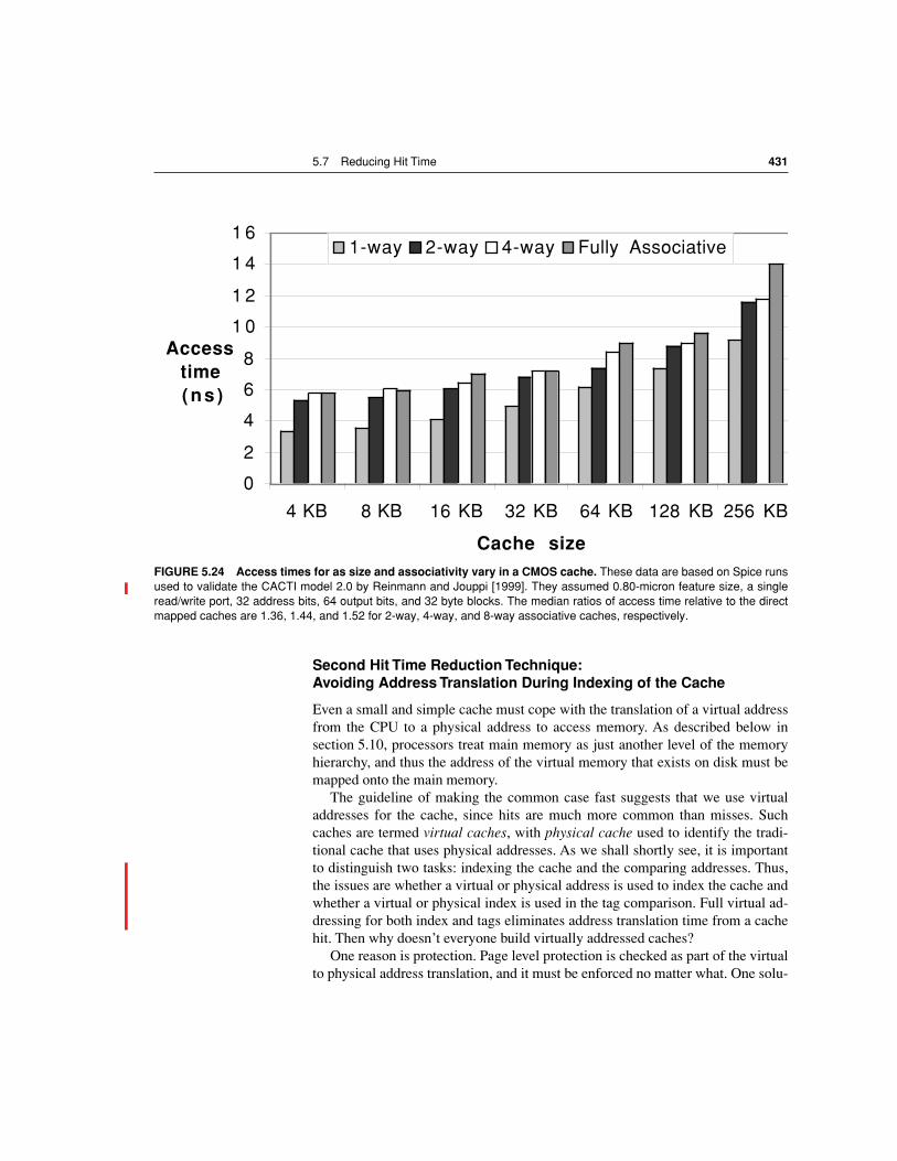
5.7 Reducing Hit Time 431
Second Hit Time Reduction Technique: Avoiding Address Translation During Indexing of the Cache
Even a small and simple cache must cope with the translation of a virtual addressfrom the CPU to a physical address to access memory. As described below insection 5.10, processors treat main memory as just another level of the memoryhierarchy, and thus the address of the virtual memory that exists on disk must bemapped onto the main memory.
The guideline of making the common case fast suggests that we use virtualaddresses for the cache, since hits are much more common than misses. Suchcaches are termed virtual caches, with physical cache used to identify the tradi-tional cache that uses physical addresses. As we shall shortly see, it is importantto distinguish two tasks: indexing the cache and the comparing addresses. Thus,the issues are whether a virtual or physical address is used to index the cache andwhether a virtual or physical index is used in the tag comparison. Full virtual ad-dressing for both index and tags eliminates address translation time from a cachehit. Then why doesn’t everyone build virtually addressed caches?
One reason is protection. Page level protection is checked as part of the virtualto physical address translation, and it must be enforced no matter what. One solu-
FIGURE 5.24 Access times for as size and associativity vary in a CMOS cache. These data are based on Spice runsused to validate the CACTI model 2.0 by Reinmann and Jouppi [1999]. They assumed 0.80-micron feature size, a singleread/write port, 32 address bits, 64 output bits, and 32 byte blocks. The median ratios of access time relative to the directmapped caches are 1.36, 1.44, and 1.52 for 2-way, 4-way, and 8-way associative caches, respectively.
0
2
4
6
8
1 0
1 2
1 4
1 6
4 KB 8 KB 16 KB 32 KB 64 KB 128 KB 256 KB
Cache size
Access time (ns )
1-way 2-way 4-way Fully Associative
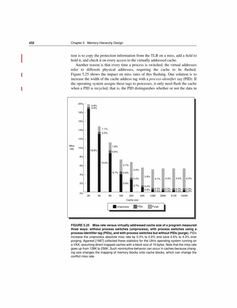
432 Chapter 5 Memory-Hierarchy Design
tion is to copy the protection information from the TLB on a miss, add a field tohold it, and check it on every access to the virtually addressed cache.
Another reason is that every time a process is switched, the virtual addressesrefer to different physical addresses, requiring the cache to be flushed.Figure 5.25 shows the impact on miss rates of this flushing. One solution is toincrease the width of the cache address tag with a process-identifier tag (PID). Ifthe operating system assigns these tags to processes, it only need flush the cachewhen a PID is recycled; that is, the PID distinguishes whether or not the data in
FIGURE 5.25 Miss rate versus virtually addressed cache size of a program measuredthree ways: without process switches (uniprocess), with process switches using aprocess-identifier tag (PIDs), and with process switches but without PIDs (purge). PIDsincrease the uniprocess absolute miss rate by 0.3% to 0.6% and save 0.6% to 4.3% overpurging. Agarwal [1987] collected these statistics for the Ultrix operating system running ona VAX, assuming direct-mapped caches with a block size of 16 bytes. Note that the miss rategoes up from 128K to 256K. Such nonintuitive behavior can occur in caches because chang-ing size changes the mapping of memory blocks onto cache blocks, which can change theconflict miss rate.
20%
18%
16%
14%
12%
10%Missrate
8%
6%
4%
2%
0%2K
0.6%0.4%
18.8%
1.1%
0.5%
13.0%
1.8%
0.6%
8.7%
2.7%
0.6%
3.9%
3.4%
0.4%
2.7%
3.9%
0.4%0.9%
4.1%
0.3%0.4%
4.3%
0.3%0.3%
4.3%
0.3%0.3%
4.3%
0.3%0.3%
4K 8K
Uniprocess PIDs Purge
16K 32K
Cache size
64K 128K 256K 512K 1024K
5.7 Reducing Hit Time 433
the cache are for this program. Figure 5.25 shows the improvement in miss ratesby using PIDs to avoid cache flushes.
A third reason why virtual caches are not more popular is that operating sys-tems and user programs may use two different virtual addresses for the samephysical address. These duplicate addresses, called synonyms or aliases, couldresult in two copies of the same data in a virtual cache; if one is modified, the oth-er will have the wrong value. With a physical cache this wouldn’t happen, sincethe accesses would first be translated to the same physical cache block.
Hardware solutions to the synonym problem, called anti-aliasing, guaranteeevery cache block a unique physical address. The Alpha 21264 uses a 64 KB in-struction cache with an 8 KB page and two-way set associativity, hence the hard-ware must handle aliases involved with the 2 virtual address bits in both sets. Itavoids aliases by simply checking all 8 possible locations on a miss–four entriesper set–to be sure that none match the physical address of the data being fetched.If one is found, it is invalidated, so when the new data is loaded into the cache itsphysical address is guaranteed to be unique.
Software can make this problem much easier by forcing aliases to share someaddress bits. The version of UNIX from Sun Microsystems, for example, requiresall aliases to be identical in the last 18 bits of their addresses; this restriction iscalled page coloring. Note that page coloring is simply set-associative mappingapplied to virtual memory: the 4-KB (212) pages are mapped using 64 (26) sets toensure that the physical and virtual addresses match in the last 18 bits. This re-striction means a direct-mapped cache that is 218 (256K) bytes or smaller cannever have duplicate physical addresses for blocks. From the perspective of thecache, page coloring effectively increases the page offset, as software guaranteesthat the last few bits of the virtual and physical page address are identical
The final area of concern with virtual addresses is I/O. I/O typically uses phys-ical addresses and thus would require mapping to virtual addresses to interactwith a virtual cache. (The impact of I/O on caches is further discussed below insection 5.12.)
One alternative to get the best of both virtual and physical caches is to use partof the page offset—the part that is identical in both virtual and physical address-es—to index the cache. At the same time as the cache is being read using that in-dex, the virtual part of the address is translated, and the tag match uses physicaladdresses.
This alternative allows the cache read to begin immediately and yet the tagcomparison is still with physical addresses. The limitation of this virtually in-dexed, physically tagged alternative is that a direct-mapped cache can be no big-ger than the page size. For example, in the data cache in Figure 5.7 on page 388,the index is 9 bits and the cache block offset is 6 bits. To use this trick, the virtualpage size would have to be at least 2(9+6) bytes or 32 KB. If not, a portion of theindex must be translated from virtual to physical address.
434 Chapter 5 Memory-Hierarchy Design
Associativity can keep the index in the physical part of the address and yet stillsupport a large cache. Recall that size of index is controlled by this formula:
For example, doubling associativity and doubling the cache size does not changethe size of the index. The Pentium III, with 8-KB pages, avoids translation withits16-KB cache by using 2-way set associativity. The IBM 3033 cache, as an ex-treme example, is 16-way set associative, even though studies show there is littlebenefit to miss rates above eight-way set associativity. This high associativity al-lows a 64-KB cache to be addressed with a physical index, despite the handicapof 4-KB pages in the IBM architecture.
Third Hit Time Reduction Technique: Pipelined Cache Access
The final technique is simply to pipeline cache access so that the effective latencyof a first level cache hit can be multiple clock cycles, giving fast cycle time andslow hits. For example, the pipeline for the Pentium takes one clock cycle to ac-cess the instruction cache, for the Pentium Pro through Pentium III it takes twoclocks, and for the Pentium 4 it takes four clocks. This split increases the numberof pipeline stages, leading to greater penalty on mispredicted branches and moreclock cycles between the issue of the load and the use of the data (see section3.9).
Note that this technique in reality increases the bandwidth of instructions rath-er that decreasing the actual latency of a cache hit.
Fourth Hit Time Reduction Technique: Trace Caches
A challenge in the effort to find instruction level parallelism beyond four instruc-tions per cycle is to supply enough instructions every cycle without dependen-cies. One solution is called a trace cache. Instead of limiting the instructions in astatic cache block to spatial locality, a trace cache finds a dynamic sequence ofinstructions including taken branches to load into a cache block.
The name comes from the cache blocks containing dynamic traces of the exe-cuted instructions as determined by the CPU rather than containing static se-quences of instructions as determined by memory. Hence, the branch predictionis folded into cache, and must be validated along with the addresses to have a val-id fetch. The Intel Netburst microarchitecture, which is the foundation of the Pen-tium 4 and its successors, uses a trace cache.
2index Cache size
Block size Set associativity×----------------------------------------------------------------------=
5.8 Main Memory and Organizations for Improving Performance 435
Clearly, trace caches have much more complicated address mapping mecha-nisms, as the addresses are no longer aligned to power of 2 multiple of the wordsize. However, they have other benefits for utilization of the data portion of theinstruction cache. Very long blocks in conventional caches may be entered from ataken branch, and hence the first portion of the block would occupy space in thecache might not be fetched. Similarly, such blocks may be exited by takenbranches, so the last portion of the block might be wasted. Given that takenbranches or jumps are one in 5 to 10 instructions, space utilization is a real prob-lem for processors like the AMD Athlon, whose 64 byte block would likelyinclude16 to 24 80x86 instructions. The trend towards even greater instruction is-sue should make the problem worse. Trace caches store instructions only fromthe branch entry point to the exit of the trace, thereby avoiding such header andtrailer overhead.
The downside of trace caches is that they store the same instructions multipletimes in the instruction cache. Conditional branches making different choices re-sult in the same instructions being part of separate traces, which each occupyspace in the cache.
Cache Optimization Summary
The techniques in sections 5.4 to 5.7 to improve miss rate, miss penalty, and hittime generally impact the other components of the average memory access equa-tion as well as the complexity of the memory hierarchy. Figure 5.26 summarizesthese techniques and estimates the impact on complexity, with + meaning that thetechnique improves the factor, – meaning it hurts that factor, and blank meaningit has no impact. Generally no technique helps more than one category.
Main memory is the next level down in the hierarchy. Main memory satisfies thedemands of caches and serves as the I/O interface, as it is the destination of inputas well as the source for output. Performance measures of main memory empha-size both latency and bandwidth. (Memory bandwidth is the number of bytesread or written per unit time.) Traditionally, main memory latency (which affectsthe cache miss penalty) is the primary concern of the cache, while main memorybandwidth is the primary concern of I/O and multiprocessors. The relationship ofmain memory and multiprocessors is discussed in Chapter 6, and relationship ofmain memory and I/O is discussed in Chapter 7.
5.8 Main Memory and Organizations for Improving Performance
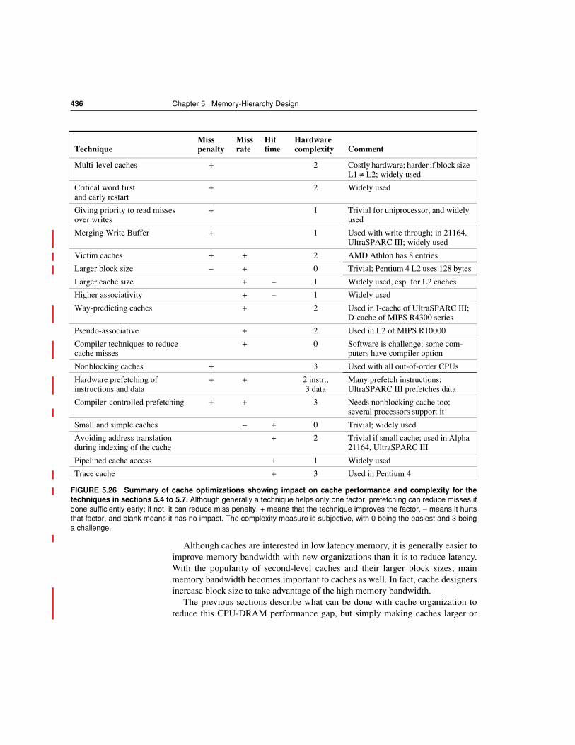
436 Chapter 5 Memory-Hierarchy Design
Although caches are interested in low latency memory, it is generally easier toimprove memory bandwidth with new organizations than it is to reduce latency.With the popularity of second-level caches and their larger block sizes, mainmemory bandwidth becomes important to caches as well. In fact, cache designersincrease block size to take advantage of the high memory bandwidth.
The previous sections describe what can be done with cache organization toreduce this CPU-DRAM performance gap, but simply making caches larger or
TechniqueMisspenalty
Missrate
Hittime
Hardware complexity Comment
Multi-level caches + 2 Costly hardware; harder if block size L1 ≠ L2; widely used
Critical word first and early restart
+ 2 Widely used
Giving priority to read misses over writes
+ 1 Trivial for uniprocessor, and widely used
Merging Write Buffer + 1 Used with write through; in 21164. UltraSPARC III; widely used
Victim caches + + 2 AMD Athlon has 8 entries
Larger block size – + 0 Trivial; Pentium 4 L2 uses 128 bytes
Larger cache size + – 1 Widely used, esp. for L2 caches
Higher associativity + – 1 Widely used
Way-predicting caches + 2 Used in I-cache of UltraSPARC III; D-cache of MIPS R4300 series
Pseudo-associative + 2 Used in L2 of MIPS R10000
Compiler techniques to reduce cache misses
+ 0 Software is challenge; some com-puters have compiler option
Nonblocking caches + 3 Used with all out-of-order CPUs
Hardware prefetching of instructions and data
+ + 2 instr., 3 data
Many prefetch instructions; UltraSPARC III prefetches data
Compiler-controlled prefetching + + 3 Needs nonblocking cache too; several processors support it
Small and simple caches – + 0 Trivial; widely used
Avoiding address translation during indexing of the cache
+ 2 Trivial if small cache; used in Alpha 21164, UltraSPARC III
Pipelined cache access + 1 Widely used
Trace cache + 3 Used in Pentium 4
FIGURE 5.26 Summary of cache optimizations showing impact on cache performance and complexity for thetechniques in sections 5.4 to 5.7. Although generally a technique helps only one factor, prefetching can reduce misses ifdone sufficiently early; if not, it can reduce miss penalty. + means that the technique improves the factor, – means it hurtsthat factor, and blank means it has no impact. The complexity measure is subjective, with 0 being the easiest and 3 beinga challenge.
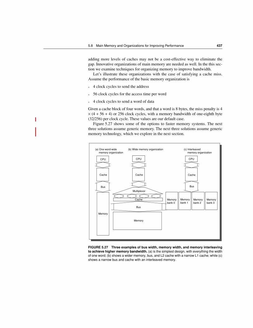
5.8 Main Memory and Organizations for Improving Performance 437
adding more levels of caches may not be a cost-effective way to eliminate thegap. Innovative organizations of main memory are needed as well. In the this sec-tion we examine techniques for organizing memory to improve bandwidth.
Let’s illustrate these organizations with the case of satisfying a cache miss.Assume the performance of the basic memory organization is
n 4 clock cycles to send the address
n 56 clock cycles for the access time per word
n 4 clock cycles to send a word of data
Given a cache block of four words, and that a word is 8 bytes, the miss penalty is 4× (4 + 56 + 4) or 256 clock cycles, with a memory bandwidth of one-eighth byte(32/256) per clock cycle. These values are our default case.
Figure 5.27 shows some of the options to faster memory systems. The nextthree solutions assume generic memory. The next three solutions assume genericmemory technology, which we explore in the next section.
FIGURE 5.27 Three examples of bus width, memory width, and memory interleavingto achieve higher memory bandwidth. (a) is the simplest design, with everything the widthof one word; (b) shows a wider memory, bus, and L2 cache with a narrow L1 cache; while (c)shows a narrow bus and cache with an interleaved memory.
Memorybank 0
Memorybank 1
Memorybank 2
Memorybank 3
Bus
Cache
CPU
(c) Interleaved memory organization
Bus
Cache
CPU
(a) One-word-wide memory organization
Cache
CPU
(b) Wide memory organization
Bus
Cache
Multiplexor
Memory
Memory
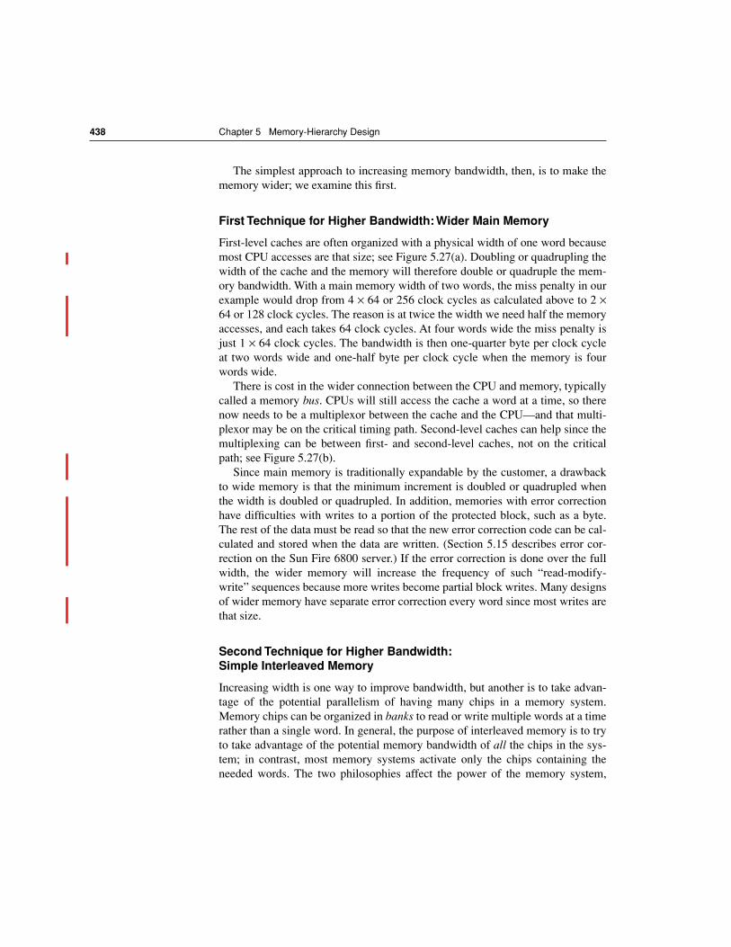
438 Chapter 5 Memory-Hierarchy Design
The simplest approach to increasing memory bandwidth, then, is to make thememory wider; we examine this first.
First Technique for Higher Bandwidth: Wider Main Memory
First-level caches are often organized with a physical width of one word becausemost CPU accesses are that size; see Figure 5.27(a). Doubling or quadrupling thewidth of the cache and the memory will therefore double or quadruple the mem-ory bandwidth. With a main memory width of two words, the miss penalty in ourexample would drop from 4 × 64 or 256 clock cycles as calculated above to 2 ×64 or 128 clock cycles. The reason is at twice the width we need half the memoryaccesses, and each takes 64 clock cycles. At four words wide the miss penalty isjust 1 × 64 clock cycles. The bandwidth is then one-quarter byte per clock cycleat two words wide and one-half byte per clock cycle when the memory is fourwords wide.
There is cost in the wider connection between the CPU and memory, typicallycalled a memory bus. CPUs will still access the cache a word at a time, so therenow needs to be a multiplexor between the cache and the CPU—and that multi-plexor may be on the critical timing path. Second-level caches can help since themultiplexing can be between first- and second-level caches, not on the criticalpath; see Figure 5.27(b).
Since main memory is traditionally expandable by the customer, a drawbackto wide memory is that the minimum increment is doubled or quadrupled whenthe width is doubled or quadrupled. In addition, memories with error correctionhave difficulties with writes to a portion of the protected block, such as a byte.The rest of the data must be read so that the new error correction code can be cal-culated and stored when the data are written. (Section 5.15 describes error cor-rection on the Sun Fire 6800 server.) If the error correction is done over the fullwidth, the wider memory will increase the frequency of such “read-modify-write” sequences because more writes become partial block writes. Many designsof wider memory have separate error correction every word since most writes arethat size.
Second Technique for Higher Bandwidth: Simple Interleaved Memory
Increasing width is one way to improve bandwidth, but another is to take advan-tage of the potential parallelism of having many chips in a memory system.Memory chips can be organized in banks to read or write multiple words at a timerather than a single word. In general, the purpose of interleaved memory is to tryto take advantage of the potential memory bandwidth of all the chips in the sys-tem; in contrast, most memory systems activate only the chips containing theneeded words. The two philosophies affect the power of the memory system,
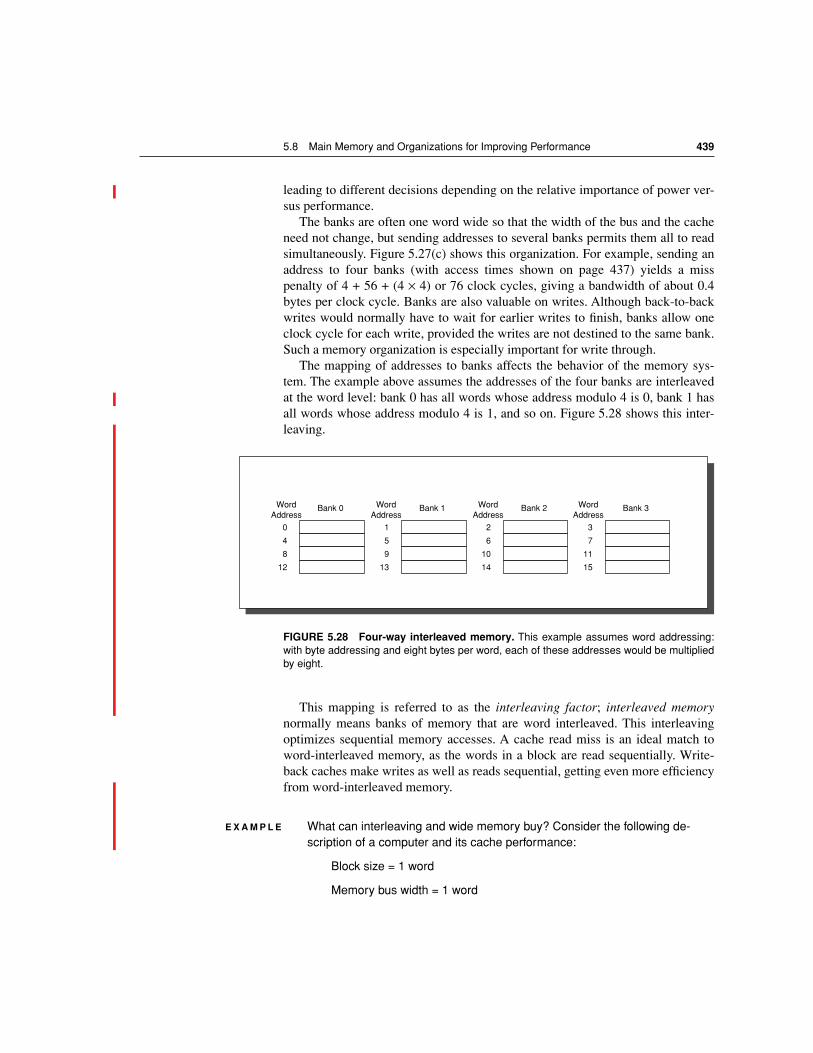
5.8 Main Memory and Organizations for Improving Performance 439
leading to different decisions depending on the relative importance of power ver-sus performance.
The banks are often one word wide so that the width of the bus and the cacheneed not change, but sending addresses to several banks permits them all to readsimultaneously. Figure 5.27(c) shows this organization. For example, sending anaddress to four banks (with access times shown on page 437) yields a misspenalty of 4 + 56 + (4 × 4) or 76 clock cycles, giving a bandwidth of about 0.4bytes per clock cycle. Banks are also valuable on writes. Although back-to-backwrites would normally have to wait for earlier writes to finish, banks allow oneclock cycle for each write, provided the writes are not destined to the same bank.Such a memory organization is especially important for write through.
The mapping of addresses to banks affects the behavior of the memory sys-tem. The example above assumes the addresses of the four banks are interleavedat the word level: bank 0 has all words whose address modulo 4 is 0, bank 1 hasall words whose address modulo 4 is 1, and so on. Figure 5.28 shows this inter-leaving.
This mapping is referred to as the interleaving factor; interleaved memorynormally means banks of memory that are word interleaved. This interleavingoptimizes sequential memory accesses. A cache read miss is an ideal match toword-interleaved memory, as the words in a block are read sequentially. Write-back caches make writes as well as reads sequential, getting even more efficiencyfrom word-interleaved memory.
E X A M P L E What can interleaving and wide memory buy? Consider the following de-scription of a computer and its cache performance:
Block size = 1 word
Memory bus width = 1 word
FIGURE 5.28 Four-way interleaved memory. This example assumes word addressing:with byte addressing and eight bytes per word, each of these addresses would be multipliedby eight.
0
4
8
12
Bank 0WordAddress
WordAddress
WordAddress
WordAddress
1
5
9
13
Bank 1
2
6
10
14
Bank 2
3
7
11
15
Bank 3
440 Chapter 5 Memory-Hierarchy Design
Miss rate = 3%
Memory accesses per instruction = 1.2
Cache miss penalty = 64 cycles (as above)
Average cycles per instruction (ignoring cache misses) = 2
If we change the block size to two words, the miss rate falls to 2%, and a four-word block has a miss rate of 1.2%. What is the improvement in per-formance of interleaving two ways and four ways versus doubling the width of memory and the bus, assuming the access times on page 437?
A N S W E R The CPI for the base computer using one-word blocks is
2 + (1.2 × 3% × 64) = 4.30
Since the clock cycle time and instruction count won’t change in this ex-ample, we can calculate performance improvement by just comparing CPI.
Increasing the block size to two words gives the following options:
64-bit bus and memory, no interleaving = 2 + (1.2 × 2% × 2 × 64) = 5.07
64-bit bus and memory, interleaving = 2 + (1.2 × 2% × (4 + 56 + 8)) = 3.63
128-bit bus and memory, no interleaving = 2 + (1.2 × 2% × 1 × 64) = 3.54
Thus, doubling the block size slows down the straightforward im-plementation (5.07 versus 4.30), while interleaving or wider memory is 1.19 or 1.22 times faster, respectively. If we increase the block size to four, the following is obtained:
64-bit bus and memory, no interleaving = 2 + (1.2 × 1.2% × 4 × 64) = 5.69
64-bit bus and memory, interleaving = 2 + (1.2 × 1.2% × (4 + 56 + 16)) = 3.09
128-bit bus and memory, no interleaving = 2 + (1.2 × 1.2% × 2 × 64) = 3.84
Again, the larger block hurts performance for the simple case (5.69 vs. 4.30), although the interleaved 64-bit memory is now fastest—1.39 times faster versus 1.22 for the wider memory and bus. n
This subsection has shown that interleaved memory is logically a wide memory,except that accesses to banks are staged over time to share internal resources—thememory bus in this example.
How many banks should be included? One metric, used in vector computers,is as follows:
Number of banks ≥ Number of clock cycles to access word in bank
5.8 Main Memory and Organizations for Improving Performance 441
The memory system goal is to deliver information from a new bank each clockcycle for sequential accesses. To see why this formula holds, imagine there werefewer banks than clock cycles to access a word in a 64-bit bank; say, 8 banks withan access time of 10 clock cycles. After 10 clock cycles the CPU could get aword from bank 0, and then bank 0 would begin fetching the next desired word asthe CPU received the following 7 words from the other 7 banks. At clock cycle18 the CPU would be at the door of bank 0, waiting for it to supply the next word.The CPU would have to wait until clock cycle 20 for the word to appear. Hence,we want more banks than clock cycles to access a bank to avoid waiting.
We will discuss conflicts on nonsequential accesses to banks in the followingsubsection. For now, we note that having many banks reduces the chance of thesebank conflicts.
Ironically, as capacity per memory chip increases, there are fewer chips in thesame-sized memory system, making multiple banks much more expensive. Forexample, a 512-MB main memory takes 256 memory chips of 4 M × 4 bit, easilyorganized into 16 banks of 16 memory chips. However, it takes only sixteen 64-M × 4-bit memory chips for 64 MB, making one bank the limit. Many manufac-turers will want to have a small memory option in the baseline model. Thisshrinking number of chips is the main disadvantage of interleaved memorybanks. Chips organized with wider paths, such as 16 M × 16 bits, postpone thisweakness.
A second disadvantage of memory banks is again the difficulty of main mem-ory expansion. Either the memory system must support multiple generations ofmemory chips, or the memory controller changes the interleaving based on thesize of physical memory, or both.
Third Technique for Higher Bandwidth: Independent Memory Banks
The original motivation for memory banks was higher memory bandwidth byinterleaving sequential accesses. This hardware is not much more difficult sincethe banks can share address lines with a memory controller, enabling each bankto use the data portion of the memory bus.
A generalization of interleaving is to allow multiple independent accesses,where multiple memory controllers allow banks (or sets of word-interleavedbanks) to operate independently. Each bank needs separate address lines and pos-sibly a separate data bus. For example, an input device may use one controllerand one bank, the cache read may use another, and a cache write may use a third.Nonblocking caches (page 421) allow the CPU to proceed beyond a cache miss,potentially allowing multiple cache misses to be serviced simultaneously. Such adesign only makes sense with memory banks; otherwise the multiple reads willbe serviced by a single memory port and get only a small benefit of overlappingaccess with transmission. Multiprocessors that share a common memory providefurther motivation for memory banks (see Chapter 6).
442 Chapter 5 Memory-Hierarchy Design
Independent of memory technology, higher bandwidth is available usingmemory banks, by making memory and its bus wider, or doing both. The nextsection examines the underlying memory technology.
… the one single development that put computers on their feet was the invention of a reliable form of memory, namely, the core memory. … Its cost was reason-able, it was reliable and, because it was reliable, it could in due course be made large. [p. 209]
Maurice Wilkes, Memoirs of a Computer Pioneer (1985)
The prior section described ways to organize memory chips; this section de-scribes the technology inside the memory chips. Before describing the options,let’s go over the performance metrics.
Memory latency is traditionally quoted using two measures—access time andcycle time. Access time is the time between when a read is requested and whenthe desired word arrives, while cycle time is the minimum time between requeststo memory. One reason that cycle time is greater than access time is that thememory needs the address lines to be stable between accesses.
DRAM technology
The main memory of virtually every desktop or server computer sold since 1975is composed of semiconductor DRAMs,.
As early DRAMs grew in capacity, the cost of a package with all the necessaryaddress lines was an issue. The solution was to multiplex the address lines, there-by cutting the number of address pins in half. Figure 5.29 shows the basic DRAMorganization. One half of the address is sent first, called the row access strobe orRAS. It is followed by the other half of the address, sent during the column accessstrobe or CAS. These names come from the internal chip organization, since thememory is organized as a rectangular matrix addressed by rows and columns.
An additional requirement of DRAM derives from the property signified by itsfirst letter, D, for dynamic. To pack more bits per chip, DRAMs use only a singletransistor to store a bit. Reading that bit can disturb the information, however. Toprevent loss of information, each bit must be “refreshed” periodically. Fortunately,all the bits in a row can be refreshed simultaneously just by reading that row.Hence, every DRAM in the memory system must access every row within a certaintime window, such as 8 milliseconds. Memory controllers include hardware to peri-odically refresh the DRAMs.
5.9 Memory Technology
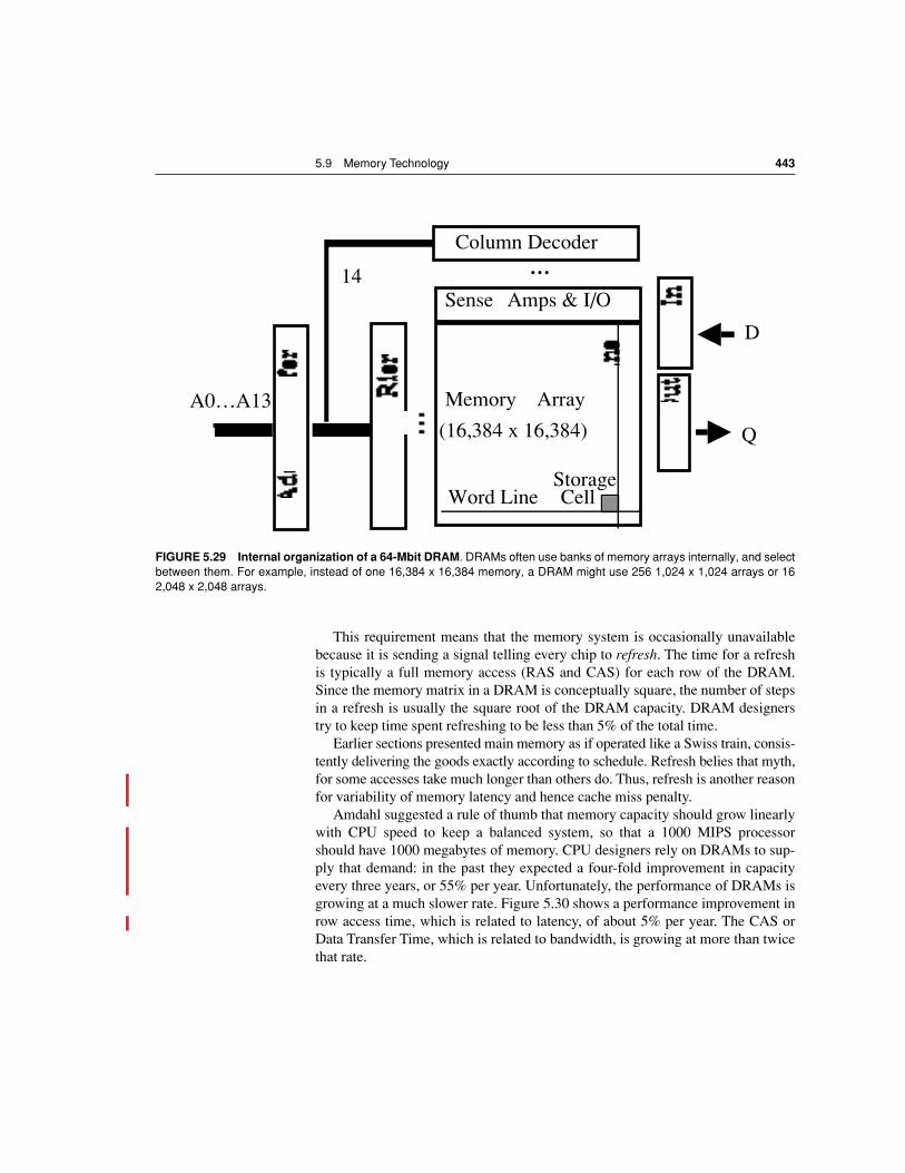
5.9 Memory Technology 443
This requirement means that the memory system is occasionally unavailablebecause it is sending a signal telling every chip to refresh. The time for a refreshis typically a full memory access (RAS and CAS) for each row of the DRAM.Since the memory matrix in a DRAM is conceptually square, the number of stepsin a refresh is usually the square root of the DRAM capacity. DRAM designerstry to keep time spent refreshing to be less than 5% of the total time.
Earlier sections presented main memory as if operated like a Swiss train, consis-tently delivering the goods exactly according to schedule. Refresh belies that myth,for some accesses take much longer than others do. Thus, refresh is another reasonfor variability of memory latency and hence cache miss penalty.
Amdahl suggested a rule of thumb that memory capacity should grow linearlywith CPU speed to keep a balanced system, so that a 1000 MIPS processorshould have 1000 megabytes of memory. CPU designers rely on DRAMs to sup-ply that demand: in the past they expected a four-fold improvement in capacityevery three years, or 55% per year. Unfortunately, the performance of DRAMs isgrowing at a much slower rate. Figure 5.30 shows a performance improvement inrow access time, which is related to latency, of about 5% per year. The CAS orData Transfer Time, which is related to bandwidth, is growing at more than twicethat rate.
FIGURE 5.29 Internal organization of a 64-Mbit DRAM. DRAMs often use banks of memory arrays internally, and selectbetween them. For example, instead of one 16,384 x 16,384 memory, a DRAM might use 256 1,024 x 1,024 arrays or 162,048 x 2,048 arrays.
Column Decoder
Sense Amps & I/O
Memory Array
(16,384 x 16,384)
A0…A13
…14
D
Q
Word LineStorage Cell
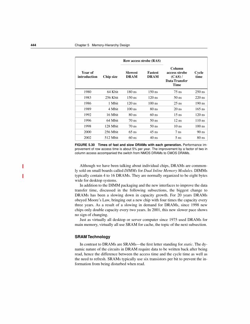
444 Chapter 5 Memory-Hierarchy Design
Although we have been talking about individual chips, DRAMs are common-ly sold on small boards called DIMMs for Dual Inline Memory Modules. DIMMstypically contain 4 to 16 DRAMs. They are normally organized to be eight byteswide for desktop systems.
In addition to the DIMM packaging and the new interfaces to improve the datatransfer time, discussed in the following subsections, the biggest change toDRAMs has been a slowing down in capacity growth. For 20 years DRAMsobeyed Moore’s Law, bringing out a new chip with four times the capacity everythree years. As a result of a slowing in demand for DRAMs, since 1998 newchips only double capacity every two years. In 2001, this new slower pace showsno sign of changing.
Just as virtually all desktop or server computer since 1975 used DRAMs formain memory, virtually all use SRAM for cache, the topic of the next subsection.
SRAM Technology
In contrast to DRAMs are SRAMs—the first letter standing for static. The dy-namic nature of the circuits in DRAM require data to be written back after beingread, hence the difference between the access time and the cycle time as well asthe need to refresh. SRAMs typically use six transistors per bit to prevent the in-formation from being disturbed when read.
Row access strobe (RAS)
Year ofintroduction Chip size
Slowest DRAM
Fastest DRAM
Columnaccess strobe
(CAS) / Data Transfer
Time
Cycletime
1980 64 Kbit 180 ns 150 ns 75 ns 250 ns
1983 256 Kbit 150 ns 120 ns 50 ns 220 ns
1986 1 Mbit 120 ns 100 ns 25 ns 190 ns
1989 4 Mbit 100 ns 80 ns 20 ns 165 ns
1992 16 Mbit 80 ns 60 ns 15 ns 120 ns
1996 64 Mbit 70 ns 50 ns 12 ns 110 ns
1998 128 Mbit 70 ns 50 ns 10 ns 100 ns
2000 256 Mbit 65 ns 45 ns 7 ns 90 ns
2002 512 Mbit 60 ns 40 ns 5 ns 80 ns
FIGURE 5.30 Times of fast and slow DRAMs with each generation. Performance im-provement of row access time is about 5% per year. The improvement by a factor of two incolumn access accompanied the switch from NMOS DRAMs to CMOS DRAMs.
5.9 Memory Technology 445
This difference in refresh alone can make a difference for embedded applica-tions. Devices often go into low power or standby mode for long periods. SRAMneeds only minimal power to retain the charge in standby mode, but DRAMsmust continue to be refreshed occasionally so as to not lose information.
In DRAM designs the emphasis is on cost per bit and capacity, while SRAMdesigns are concerned with speed and capacity. (Because of this concern, SRAMaddress lines are not multiplexed.). Thus, unlike DRAMs, there is no differencebetween access time and cycle time. For memories designed in comparabletechnologies, the capacity of DRAMs is roughly 4 to 8 times that of SRAMs. Thecycle time of SRAMs is 8 to 16 times faster than DRAMs, but they are also 8 to16 times as expensive.
Embedded Processor Memory Technology: ROM and Flash
Embedded computers usually have small memories, and most do not have a diskto act as non-volatile storage. Two memory technologies are found in embeddedcomputers to address this problem.
The first is Read-Only Memory (ROM). ROM is programmed at time of manu-facture, needing only a single transistor per bit to represent 1 or 0. ROM is usedfor the embedded program and for constants, often included as part of a largerchip.
In addition to being non-volatile, ROM is also non-destructible; nothing thecomputer can do can modify the contents of this memory. Hence, ROM also pro-vides a level of protection to the code of embedded computers. Since address-based protection is often not enabled in embedded processors, ROM can fulfill animportant role.
The second memory technology offers non-volatility but allows the memoryto be modified. Flash memory allows the embedded device to alter nonvolatilememory after the system is manufactured, which can shorten product develop-ment. Flash memory, described in on page 498 in Chapter 7, allows reading at al-most DRAM speeds but writing flash is 10 to 100 times slower. In 2001, theDRAM capacity per chip and the megabytes per dollar is about four to eighttimes greater than flash memory.
Improving Memory Performance in a standard DRAM Chip
As Moore’s Law continues to supply more transistors and as the processor-mem-ory gap increases pressure on memory performance, some of the ideas of the pri-or section have made their way inside the DRAM chip. Generally the idea hasbeen for greater bandwidth, often at the cost of greater latency. This subsectionpresents techniques that take advantage of the nature of DRAMs.
As mentioned earlier, a DRAM access is divided into row access and columnaccess. DRAMs must buffer a row of bits inside the DRAM for the columnaccess, and this row is usually the square root of the DRAM size—8 Kbits for 64Mbits, 16 Kbits for 256 Mbits, and so on.
446 Chapter 5 Memory-Hierarchy Design
Although presented logically as a single monolithic array of memory bits, theinternal organization of DRAM actually consists of many memory modules. Fora variety of manufacturing reasons, these modules are usually 1 to 4 megabits.Thus, if you were to examine a 256 Mbit DRAM under a microscope, you mightsee 128 2-megabit memory arrays on the chip. This large number of arrays inter-nally presents the opportunity to provide much higher bandwidth off chip.
To improve bandwidth, there have been a variety of evolutionary innovationsover time. The first was timing signals that allow repeated accesses to the rowbuffer without another row access time, typically called fast page mode. Such abuffer comes naturally, as each array will buffer 1024 to 2048 bits for each ac-cess.
The second major change is that conventional DRAMs have an asynchronousinterface to the memory controller, and hence every transfer involves overhead tosynchronize with the controller. The solution was to add a clock signal to theDRAM interface, so that the repeated transfers would not bear that overhead.This optimization is called Synchronous DRAM, abbreviated SDRAM. SDRAMstypically also have a programmable register to hold the number of bytes request-ed, and hence can send many bytes over several cycles per request.
In 2001 the bus rates are 100 MHz to 150 MHz. SDRAM DIMMs of thesespeeds are called PC100, PC133, and PC 150, based on the clock speed of the in-dividual chip. Multiplying the eight-byte width of the DIMM times the clockrate, the peak speed per memory module is 800 to 1200 MB/sec.
The third major DRAM innovation to increase bandwidth is to transfer data onboth the rising edge and falling edge of the DRAM clock signal, thereby dou-bling the peak data rate. This optimization is called Double Data Rate, and abbre-viated DDR. The bus speeds for these DRAMs are also 100 to 150 MHz, butthese DDR DIMMs are confusingly labeled by the peak DIMM bandwidth. Thename PC1600 comes from100 MHz × 2 × 8 bytes or 1600 Megabytes/second,133 MHz leads to PC2100, 150 MHz yields PC2400, and so on.
In each of the three cases the advantage of such optimizations is that they adda small amount of logic to exploit the high internal DRAM bandwidth, adding lit-tle cost to the system while achieving a significant improvement in bandwidth.Unlike traditional interleaved memories, there is no danger in using such a modeas DRAM chips increase in capacity.
Improving Memory Performance via a new DRAM Interface: RAMBUS
Recently new breeds of DRAMs have been produced that further optimize theinterface between the DRAM and CPU. The company RAMBUS takes the stan-dard DRAM core and provides a new interface, making a single chip act morelike a memory system than a memory component: each chip has interleavedmemory and a high speed interface. RAMBUS licenses its technology to compa-nies that use its interface, both DRAM and microprocessor manufacturers.
5.9 Memory Technology 447
The first generation RAMBUS interface dropped RAS/CAS, replacing it witha bus that allows other accesses over the bus between the sending of the addressand return of the data. It is typically called RDRAM. (Such a bus is called apacket-switched bus or split-transaction bus, described in Chapters 7 and 8.)This bus allows a single chip to act as a memory bank. A chip can return a vari-able amount of data from a single request, and even perform its own refresh.RDRAM offered a byte-wide interface, and was one of the first DRAMs to use aclock signal, and it also transfers on both edges of its clock. Inside each chipwere four banks, each with their own row buffer. To run at its 300 Mhz clock,the RAMBUS bus is limited to be no more than 4 inches long. Typically a mi-croprocessor uses a single RAMBUS channel, so just one RDRAM is transfer-ring at a time.
The second generation RAMBUS interface, called Direct RDRAM orDRDRAM, offers up to 1.6 GBytes/second of bandwidth from a single DRAM.Innovations in this interface include a separate row- and column-command busesinstead of the conventional multiplexing; an 18-bit data bus; expanding from 4 to16 internal banks per RDRAM to reduce bank conflicts; increasing the number ofrow buffers from 4 to 8; increasing the clock to 400 MHz clock; and a much moresophisticated controller on chip. Because of the separation of data, row, and col-umn buses, three transactions can be performed simultaneously.
RAMBUS helped set the new optimistic naming trend, calling the 350 MHzpart PC700, the 400 MHz part PC800, and so on. Since each chip is 2 byteswide, the peak chip bandwidth of PC700 is 1400 MB/second, PC800 is 1600MB/second, and so on. RAMBUS chips are not sold in DIMMs but in “RIMMs”which is similar in size but incompatible with DIMMs. RIMMs are designed tohave a single RAMBUS chip on the RIMM supply the memory bandwidth needsof the computer, and are not interchangeable with DIMMs.
Comparing RAMBUS and DDR SDRAM
How does the RAMBUS interface compare in cost and performance when placedin a system? Most main memory systems already use SDRAM to get more bitsper memory access, in the hope of reducing the CPU-DRAM performance gap.Since the most computers use memory in DIMM packages, which are typically atleast 64-bits wide, the DIMM memory bandwidth is closer to what RAMBUSprovides than you might expect when just comparing DRAM chips.
The one note of caution is that performance of cache based systems are basedin part on latency to the first byte and in part on the bandwidth to deliver the restof the bytes in the block. Although these innovations help with the latter case,none help with latency. Amdahl’s Law reminds us of the limits of acceleratingone piece of the problem while ignoring another part.
In addition to performance, the new breed of DRAMs such as RDRAM andDRDRAM have price a premium over traditional DRAMs to provide the greater
448 Chapter 5 Memory-Hierarchy Design
bandwidth since these chips are larger. The question over time is how muchmore. In 2001 it is factor of two; Section 5.16 has a detailed price-performanceevaluation.
The marketplace will determine whether the more radical DRAMs such asRAMBUS will become popular for main memory, or whether the price premiumrestricts them to niche markets.
… a system has been devised to make the core drum combination appear to the programmer as a single level store, the requisite transfers taking place automatically.
Kilburn et al. [1962]
At any instant in time computers are running multiple processes, each with itsown address space. (Processes are described in the next section.) It would be tooexpensive to dedicate a full-address-space worth of memory for each process, es-pecially since many processes use only a small part of their address space. Hence,there must be a means of sharing a smaller amount of physical memory amongmany processes. One way to do this, virtual memory, divides physical memoryinto blocks and allocates them to different processes. Inherent in such an ap-proach must be a protection scheme that restricts a process to the blocks belong-ing only to that process. Most forms of virtual memory also reduce the time tostart a program, since not all code and data need be in physical memory before aprogram can begin.
Although protection provided by virtual memory is essential for current com-puters, sharing is not the reason that virtual memory was invented. If a programbecame too large for physical memory, it was the programmer’s job to make it fit.Programmers divided programs into pieces, then identified the pieces that weremutually exclusive, and loaded or unloaded these overlays under user programcontrol during execution. The programmer ensured that the program never triedto access more physical main memory than was in the computer, and that theproper overlay was loaded at the proper time. As one can well imagine, this re-sponsibility eroded programmer productivity.
Virtual memory was invented to relieve programmers of this burden; it auto-matically manages the two levels of the memory hierarchy represented by mainmemory and secondary storage. Figure 5.31 shows the mapping of virtual memo-ry to physical memory for a program with four pages.
In addition to sharing protected memory space and automatically managingthe memory hierarchy, virtual memory also simplifies loading the program forexecution. Called relocation, this mechanism allows the same program to run inany location in physical memory. The program in Figure 5.31 can be placed any-
5.10 Virtual Memory
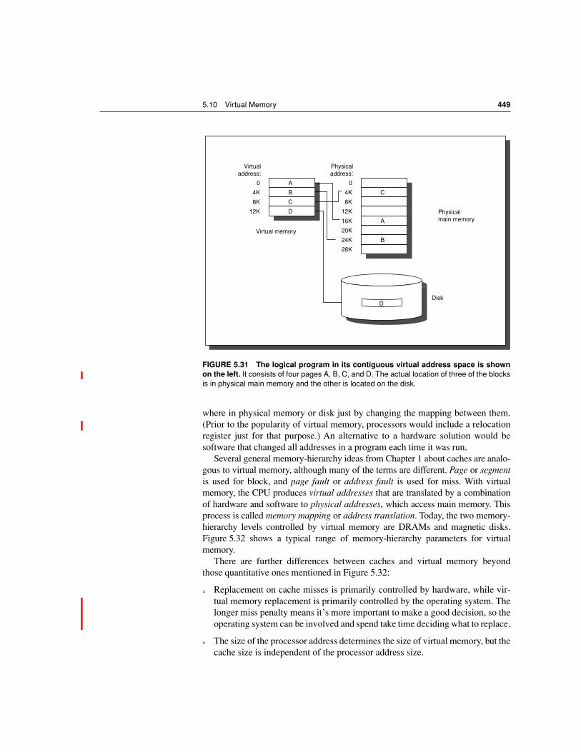
5.10 Virtual Memory 449
where in physical memory or disk just by changing the mapping between them.(Prior to the popularity of virtual memory, processors would include a relocationregister just for that purpose.) An alternative to a hardware solution would besoftware that changed all addresses in a program each time it was run.
Several general memory-hierarchy ideas from Chapter 1 about caches are analo-gous to virtual memory, although many of the terms are different. Page or segmentis used for block, and page fault or address fault is used for miss. With virtualmemory, the CPU produces virtual addresses that are translated by a combinationof hardware and software to physical addresses, which access main memory. Thisprocess is called memory mapping or address translation. Today, the two memory-hierarchy levels controlled by virtual memory are DRAMs and magnetic disks.Figure 5.32 shows a typical range of memory-hierarchy parameters for virtualmemory.
There are further differences between caches and virtual memory beyondthose quantitative ones mentioned in Figure 5.32:
n Replacement on cache misses is primarily controlled by hardware, while vir-tual memory replacement is primarily controlled by the operating system. Thelonger miss penalty means it’s more important to make a good decision, so theoperating system can be involved and spend take time deciding what to replace.
n The size of the processor address determines the size of virtual memory, but thecache size is independent of the processor address size.
FIGURE 5.31 The logical program in its contiguous virtual address space is shownon the left. It consists of four pages A, B, C, and D. The actual location of three of the blocksis in physical main memory and the other is located on the disk.
0
4K
8K
12K
16K
20K
24K
28K
Physicaladdress:
Physicalmain memory
DiskD
0
4K
8K
12K
Virtualaddress:
Virtual memory
A
B
C
D
C
A
B
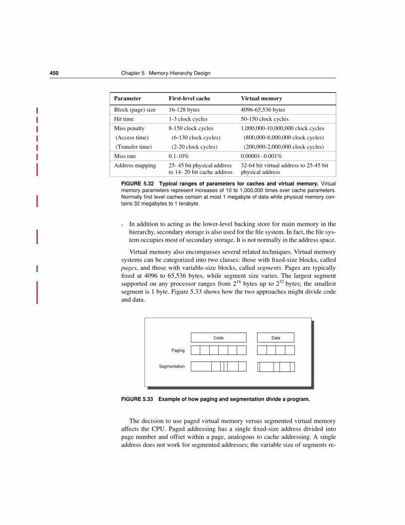
450 Chapter 5 Memory-Hierarchy Design
n In addition to acting as the lower-level backing store for main memory in thehierarchy, secondary storage is also used for the file system. In fact, the file sys-tem occupies most of secondary storage. It is not normally in the address space.
Virtual memory also encompasses several related techniques. Virtual memorysystems can be categorized into two classes: those with fixed-size blocks, calledpages, and those with variable-size blocks, called segments. Pages are typicallyfixed at 4096 to 65,536 bytes, while segment size varies. The largest segmentsupported on any processor ranges from 216 bytes up to 232 bytes; the smallestsegment is 1 byte. Figure 5.33 shows how the two approaches might divide codeand data.
The decision to use paged virtual memory versus segmented virtual memoryaffects the CPU. Paged addressing has a single fixed-size address divided intopage number and offset within a page, analogous to cache addressing. A singleaddress does not work for segmented addresses; the variable size of segments re-
Parameter First-level cache Virtual memory
Block (page) size 16-128 bytes 4096-65,536 bytes
Hit time 1-3 clock cycles 50-150 clock cycles
Miss penalty 8-150 clock cycles 1,000,000-10,000,000 clock cycles
(Access time) (6-130 clock cycles) (800,000-8,000,000 clock cycles)
(Transfer time) (2-20 clock cycles) (200,000-2,000,000 clock cycles)
Miss rate 0.1-10% 0.00001- 0.001%
Address mapping 25- 45 bit physical address to 14- 20 bit cache address
32-64 bit virtual address to 25-45 bit physical address
FIGURE 5.32 Typical ranges of parameters for caches and virtual memory. Virtualmemory parameters represent increases of 10 to 1,000,000 times over cache parameters.Normally first level caches contain at most 1 megabyte of data while physical memory con-tains 32 megabytes to 1 terabyte.
FIGURE 5.33 Example of how paging and segmentation divide a program.
Code Data
Paging
Segmentation
5.10 Virtual Memory 451
quires one word for a segment number and one word for an offset within a seg-ment, for a total of two words. An unsegmented address space is simpler for thecompiler.
The pros and cons of these two approaches have been well documented inoperating systems textbooks; Figure 5.34 summarizes the arguments. Because ofthe replacement problem (the third line of the figure), few computers today usepure segmentation. Some computers use a hybrid approach, called pagedsegments, in which a segment is an integral number of pages. This simplifies re-placement because memory need not be contiguous, and the full segments neednot be in main memory. A more recent hybrid is for a computer to offer multiplepage sizes, with the larger sizes being powers of two times the smallest page size.The IBM 405CR embedded processor, for example, allows 1 KB, 4 KB (22 × 1KB), 16 KB (24 × 1 KB), 64 KB (26 × 1 KB), 256 KB (28 × 1 KB), 1024 KB (210
× 1 KB), and 4096 KB (212 × 1 KB) to act as a single page.
We are now ready to answer the four memory-hierarchy questions for virtualmemory.
Q1: Where can a block be placed in main memory?The miss penalty for virtual memory involves access to a rotating magnetic stor-age device and is therefore quite high. Given the choice of lower miss rates or asimpler placement algorithm, operating systems designers normally pick lowermiss rates because of the exorbitant miss penalty. Thus, operating systems allowblocks to be placed anywhere in main memory. According to the terminology inFigure 5.4 (page 382), this strategy would be labeled fully associative.
Page Segment
Words per address One Two (segment and offset)
Programmer visible? Invisible to application programmer May be visible to application programmer
Replacing a block Trivial (all blocks are the same size) Hard (must find contiguous, variable-size, unused portion of main memory)
Memory use inefficiency
Internal fragmentation (unused portion of page)
External fragmentation (unused pieces of main memory)
Efficient disk traffic Yes (adjust page size to balance access time and transfer time)
Not always (small segments may transfer just a few bytes)
FIGURE 5.34 Paging versus segmentation. Both can waste memory, depending on the block size and how well the seg-ments fit together in main memory. Programming languages with unrestricted pointers require both the segment and theaddress to be passed. A hybrid approach, called paged segments, shoots for the best of both worlds: segments are com-posed of pages, so replacing a block is easy, yet a segment may be treated as a logical unit.
452 Chapter 5 Memory-Hierarchy Design
Q2: How is a block found if it is in main memory?Both paging and segmentation rely on a data structure that is indexed by the pageor segment number. This data structure contains the physical address of theblock. For segmentation, the offset is added to the segment’s physical address toobtain the final physical address. For paging, the offset is simply concatenated tothis physical page address (see Figure 5.35).
This data structure, containing the physical page addresses, usually takes theform of a page table. Indexed by the virtual page number, the size of the table isthe number of pages in the virtual address space. Given a 32-bit virtual address,4-KB pages, and 4 bytes per page table entry, the size of the page table would be(232/212) × 22 = 222 or 4 MB.
To reduce the size of this data structure, some computers apply a hashingfunction to the virtual address. The hash allows the data structure to be the lengthof the number of physical pages in main memory. This number could be muchsmaller than the number of virtual pages. Such a structure is called an invertedpage table. Using the example above, a 512-MB physical memory would onlyneed 1 MB (8 × 512 MB/4 KB) for an inverted page table; the extra 4 bytes perpage table entry is for the virtual address. The HP/Intel IA-64 covers both basesby offering both traditional pages tables and inverted page tables, leaving thechoice of mechanism to the operating system programmer.
FIGURE 5.35 The mapping of a virtual address to a physical address via a page table.
Main memory
Pagetable
Virtual address
Virtual page number Page offset
Physical address
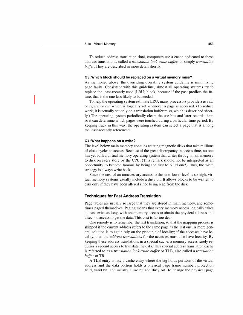
5.10 Virtual Memory 453
To reduce address translation time, computers use a cache dedicated to theseaddress translations, called a translation look-aside buffer, or simply translationbuffer. They are described in more detail shortly.
Q3: Which block should be replaced on a virtual memory miss? As mentioned above, the overriding operating system guideline is minimizingpage faults. Consistent with this guideline, almost all operating systems try toreplace the least-recently used (LRU) block, because if the past predicts the fu-ture, that is the one less likely to be needed.
To help the operating system estimate LRU, many processors provide a use bitor reference bit, which is logically set whenever a page is accessed. (To reducework, it is actually set only on a translation buffer miss, which is described short-ly.) The operating system periodically clears the use bits and later records themso it can determine which pages were touched during a particular time period. Bykeeping track in this way, the operating system can select a page that is amongthe least-recently referenced.
Q4: What happens on a write? The level below main memory contains rotating magnetic disks that take millionsof clock cycles to access. Because of the great discrepancy in access time, no onehas yet built a virtual memory operating system that writes through main memoryto disk on every store by the CPU. (This remark should not be interpreted as anopportunity to become famous by being the first to build one!) Thus, the writestrategy is always write back.
Since the cost of an unnecessary access to the next-lower level is so high, vir-tual memory systems usually include a dirty bit. It allows blocks to be written todisk only if they have been altered since being read from the disk.
Techniques for Fast Address Translation
Page tables are usually so large that they are stored in main memory, and some-times paged themselves. Paging means that every memory access logically takesat least twice as long, with one memory access to obtain the physical address anda second access to get the data. This cost is far too dear.
One remedy is to remember the last translation, so that the mapping process isskipped if the current address refers to the same page as the last one. A more gen-eral solution is to again rely on the principle of locality; if the accesses have lo-cality, then the address translations for the accesses must also have locality. Bykeeping these address translations in a special cache, a memory access rarely re-quires a second access to translate the data. This special address translation cacheis referred to as a translation look-aside buffer or TLB, also called a translationbuffer or TB.
A TLB entry is like a cache entry where the tag holds portions of the virtualaddress and the data portion holds a physical page frame number, protectionfield, valid bit, and usually a use bit and dirty bit. To change the physical page
454 Chapter 5 Memory-Hierarchy Design
frame number or protection of an entry in the page table, the operating systemmust make sure the old entry is not in the TLB; otherwise, the system won’t be-have properly. Note that this dirty bit means the corresponding page is dirty, notthat the address translation in the TLB is dirty nor that a particular block in thedata cache is dirty. The operating system resets these bits by changing the valuein the page table and then invalidating the corresponding TLB entry. When theentry is reloaded from the page table, the TLB gets an accurate copy of the bits.
Figure 5.36 shows the Alpha 21264 data TLB organization, with each step of atranslation labeled. The TLB uses fully associative placement; thus, the transla-tion begins (steps 1 and 2) by sending the virtual address to all tags. Of course,the tag must be marked valid to allow a match. At the same time, the type ofmemory access is checked for a violation (also in step 2) against protection infor-mation in the TLB.
To reduce TLB misses due to context switches, each entry has an 8-bit Ad-dress Space Number or ASN, which plays the same role as a Process ID number
FIGURE 5.36 Operation of the Alpha 21264 data TLB during address translation. Thefour steps of a TLB hit are shown as circled numbers. The Address Space Number (ASN) isused like a Process ID for virtual caches, in that the TLB is not flushed on a context switch,only when ASNs are recycled. The next fields of an entry are protection permissions (Prot)and the valid bit (V). Note that there is no specific reference, use bit, or dirty bit. Hence, apage replacement algorithm such as LRU must rely on disabling reads and writes occasion-ally to record reads and writes to pages to measure usage and whether or not pages are dirty.The advantage of these omissions is that the TLB need not be written during normal memoryaccesses nor during a TLB miss. Alpha 21264 has an option of either 44-bit or 41-bit physicaladdresses. This TLB has 128 entries.
Virtual page number<35>
Address Space Number
<8>
Pageoffset<13>
ASN Physical address<8> <4> <31>
Prot Tag<35>
V<1>
<31 or 28 >
<13>44- or 41-bitphysicaladdress
43
21
(Low-order 13 bits of address)
(High-order 31/28 bits of address)
128:1 Mux
5.10 Virtual Memory 455
mentioned in Figure 5.25 on page 432. If the context switching returns to the pro-cess with the same ASN, it can still match the TLB. Thus, the process ASN andthe PTE ASN must also match for a valid tag.
For reasons similar to those in the cache case, there is no need to include the13 bits of the Alpha 21264 page offset in the TLB. The matching tag sends thecorresponding physical address through effectively a 128:1 multiplexor (step 3).The page offset is then combined with the physical page frame to form a fullphysical address (step 4). The address size is 44 or 41 bits depending on a physi-cal address mode bit (see section 5.11).
Address translation can easily be on the critical path determining the clockcycle of the processor, so the 21264 uses a virtually addressed instruction cache,thus the TLB is only accessed during an instruction cache miss.
Selecting a Page Size
The most obvious architectural parameter is the page size. Choosing the page is aquestion of balancing forces that favor a larger page size versus those favoring asmaller size. The following favor a larger size:
n The size of the page table is inversely proportional to the page size; memory(or other resources used for the memory map) can therefore be saved by mak-ing the pages bigger.
n As mentioned on page 433 in section 5.7, a larger page size can allow largercaches with fast cache hit times.
n Transferring larger pages to or from secondary storage, possibly over a net-work, is more efficient than transferring smaller pages.
n The number of TLB entries are restricted, so a larger page size means that morememory can be mapped efficiently, thereby reducing the number of TLB misses.
It is for this final reason that recent microprocessors have decided to support mul-tiple page sizes; for some programs, TLB misses can be as significant on CPI asthe cache misses.
The main motivation for a smaller page size is conserving storage. A smallpage size will result in less wasted storage when a contiguous region of virtualmemory is not equal in size to a multiple of the page size. The term for this un-used memory in a page is internal fragmentation. Assuming that each process hasthree primary segments (text, heap, and stack), the average wasted storage perprocess will be 1.5 times the page size. This amount is negligible for computerswith hundreds of megabytes of memory and page sizes of 4 KB to 8 KB. Ofcourse, when the page sizes become very large (more than 32 KB), lots of storage(both main and secondary) may be wasted, as well as I/O bandwidth. A final con-cern is process start-up time; many processes are small, so a large page sizewould lengthen the time to invoke a process
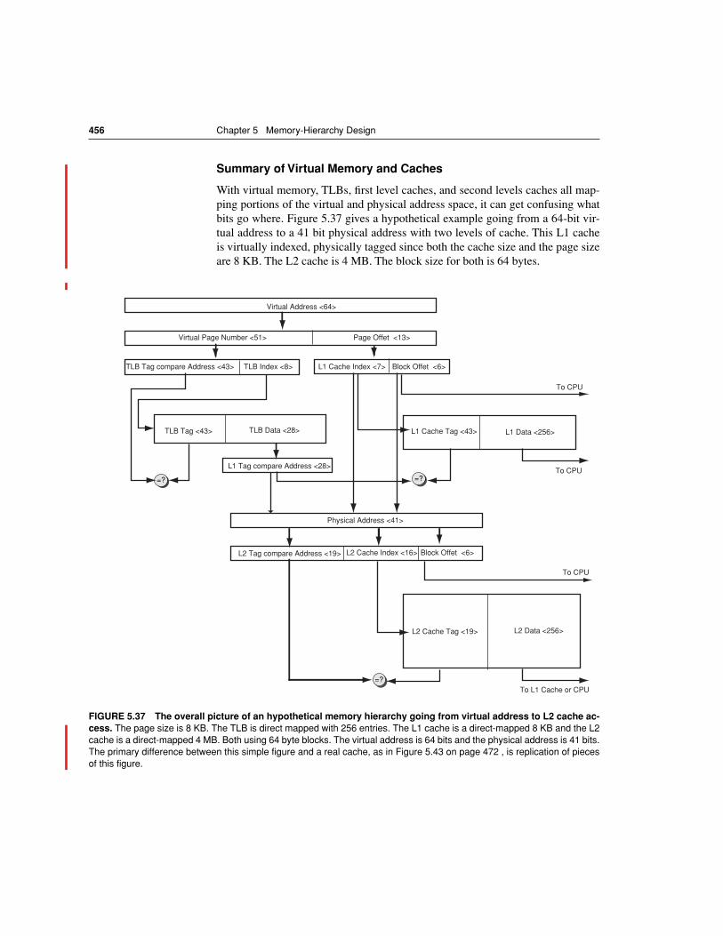
456 Chapter 5 Memory-Hierarchy Design
Summary of Virtual Memory and Caches
With virtual memory, TLBs, first level caches, and second levels caches all map-ping portions of the virtual and physical address space, it can get confusing whatbits go where. Figure 5.37 gives a hypothetical example going from a 64-bit vir-tual address to a 41 bit physical address with two levels of cache. This L1 cacheis virtually indexed, physically tagged since both the cache size and the page sizeare 8 KB. The L2 cache is 4 MB. The block size for both is 64 bytes.
FIGURE 5.37 The overall picture of an hypothetical memory hierarchy going from virtual address to L2 cache ac-cess. The page size is 8 KB. The TLB is direct mapped with 256 entries. The L1 cache is a direct-mapped 8 KB and the L2cache is a direct-mapped 4 MB. Both using 64 byte blocks. The virtual address is 64 bits and the physical address is 41 bits.The primary difference between this simple figure and a real cache, as in Figure 5.43 on page 472 , is replication of piecesof this figure.
Virtual Address <64>
Physical Address <41>
Virtual Page Number <51>
L1 Tag compare Address <28>
L2 Tag compare Address <19> L2 Cache Index <16> Block Offet <6>
Page Offet <13>
L1 Cache Tag <43> L1 Data <256>TLB Tag <43> TLB Data <28>
L1 Cache Index <7> Block Offet <6>TLB Tag compare Address <43> TLB Index <8>
L2 Cache Tag <19> L2 Data <256>
=? =?
=?
To CPU
To CPU
To CPU
To L1 Cache or CPU
5.11 Protection and Examples of Virtual Memory 457
First, the 64-bit virtual address is logically divided into a virtual page numberand page offset. The former is sent to the TLB to be translated into a physical ad-dress, and the latter is sent to the L1 cache act as an index. If the TLB match is ahit, then the physical page number is sent to the L1 cache tag to check for amatch. If it matches, its a L1 cache hit. The block offset then selects the word forthe CPU.
If the L1 cache check results in a miss, the physical address is then used to trythe L2 cache. The middle portion of the physical address is used as an index tothe 4 MB L2 cache. The resulting L2 Cache Tag is compared to the upper part ofthe physical address to check for a match. If it matches, we have a L2 cache hit,and the data is sent to the CPU, which uses the block offset to select the desiredword. On an L2 miss, the physical address is then used to get the block frommemory.
Although this is a simple example, the major difference between this drawingand a real cache is replication. First, there is only one L1 cache. When there aretwo L1 caches, the top half of the diagram is duplicated. Note this would lead totwo TLBs, which is typical. Hence, one cache and TLB is for instructions, drivenfrom the PC, and one cache and TLB is for data, driven from the effective ad-dress. The second simplification is that all the caches and TLBs are directmapped. If any were N-way set associative, then we would replicate each set oftag memory, comparators, and data memory N times and connect data memorieswith a N:1 multiplexor to select a hit. Of course, if the total cache size remainedthe same, the cache index would also shrink by N bits according to the formula inFigure 5.9 on page 397 .
The invention of multiprogramming, where a computer would be shared byseveral programs running concurrently, led to new demands for protection andsharing among programs. These demands are closely tied to virtual memory incomputers today, and so we cover the topic here along with two examples of vir-tual memory.
Multiprogramming leads to the concept of a process. Metaphorically, a pro-cess is a program’s breathing air and living space—that is, a running programplus any state needed to continue running it. Time-sharing is a variation of multi-programming that shares the CPU and memory with several interactive users atthe same time, giving the illusion that all users have their own computers. Thus,at any instant it must be possible to switch from one process to another. This ex-change is called a process switch or context switch.
A process must operate correctly whether it executes continuously from startto finish, or is interrupted repeatedly and switched with other processes. The re-sponsibility for maintaining correct process behavior is shared by designers of
5.11 Protection and Examples of Virtual Memory
458 Chapter 5 Memory-Hierarchy Design
the computer and the operating system. The computer designer must ensure thatthe CPU portion of the process state can be saved and restored. The operatingsystem designer must guarantee that processes do not interfere with each others’computations.
The safest way to protect the state of one process from another would be tocopy the current information to disk. However, a process switch would then takeseconds—far too long for a time-sharing environment.
This problem is solved by operating systems partitioning main memory so thatseveral different processes have their state in memory at the same time. This divi-sion means that the operating system designer needs help from the computer de-signer to provide protection so that one process cannot modify another. Besidesprotection, the computers also provide for sharing of code and data between pro-cesses, to allow communication between processes or to save memory by reduc-ing the number of copies of identical information.
Protecting Processes
The simplest protection mechanism is a pair of registers that checks every ad-dress to be sure that it falls between the two limits, traditionally called base andbound. An address is valid if
Base ≤ Address ≤ Bound
In some systems, the address is considered an unsigned number that is alwaysadded to the base, so the limit test is just
(Base + Address) ≤ Bound
If user processes are allowed to change the base and bounds registers, thenusers can’t be protected from each other. The operating system, however, must beable to change the registers so that it can switch processes. Hence, the computerdesigner has three more responsibilities in helping the operating system designerprotect processes from each other:
1. Provide at least two modes, indicating whether the running process is a userprocess or an operating system process. This latter process is sometimes calleda kernel process, a supervisor process, or an executive process.
2. Provide a portion of the CPU state that a user process can use but not write.This state includes the base/bound registers, a user/supervisor mode bit(s), andthe exception enable/disable bit. Users are prevented from writing this statebecause the operating system cannot control user processes if users can changethe address range checks, give themselves supervisor privileges, or disableexceptions.
3. Provide mechanisms whereby the CPU can go from user mode to supervisor
5.11 Protection and Examples of Virtual Memory 459
mode and vice versa. The first direction is typically accomplished by a systemcall, implemented as a special instruction that transfers control to a dedicatedlocation in supervisor code space. The PC is saved from the point of the sys-tem call, and the CPU is placed in supervisor mode. The return to user modeis like a subroutine return that restores the previous user/supervisor mode.
Base and bound constitute the minimum protection system, while virtualmemory offers a more fine-grained alternative to this simple model. As we haveseen, the CPU address must be mapped from virtual to physical address. Thismapping provides the opportunity for the hardware to check further for errors inthe program or to protect processes from each other. The simplest way of doingthis is to add permission flags to each page or segment. For example, since fewprograms today intentionally modify their own code, an operating system can de-tect accidental writes to code by offering read-only protection to pages. Thispage-level protection can be extended by adding user/kernel protection to preventa user program from trying to access pages that belong to the kernel. As long asthe CPU provides a read/write signal and a user/kernel signal, it is easy for theaddress translation hardware to detect stray memory accesses before they can dodamage. Such reckless behavior simply interrupts the CPU and invokes the oper-ating system.
Processes are thus protected from one another by having their own pagetables, each pointing to distinct pages of memory. Obviously, user programs mustbe prevented from modifying their page tables or protection would be circum-vented.
Protection can be escalated, depending on the apprehension of the computerdesigner or the purchaser. Rings added to the CPU protection structure expandmemory access protection from two levels (user and kernel) to many more. Likea military classification system of top secret, secret, confidential, and unclassi-fied, concentric rings of security levels allow the most trusted to access anything,the second most trusted to access everything except the innermost level, and soon. The “civilian” programs are the least trusted and, hence, have the most limit-ed range of accesses. There may also be restrictions on what pieces of memorycan contain code—execute protection—and even on the entrance point betweenthe levels. The Intel Pentium protection structure, which uses rings, is describedlater in this section. It is not clear whether rings are an improvement in practiceover the simple system of user and kernel modes.
As the designer’s apprehension escalates to trepidation, these simple rings maynot suffice. Restricting the freedom given a program in the inner sanctum requiresa new classification system. Instead of a military model, the analogy of this systemis to keys and locks: A program can’t unlock access to the data unless it has thekey. For these keys, or capabilities, to be useful, the hardware and operating sys-tem must be able to explicitly pass them from one program to another without
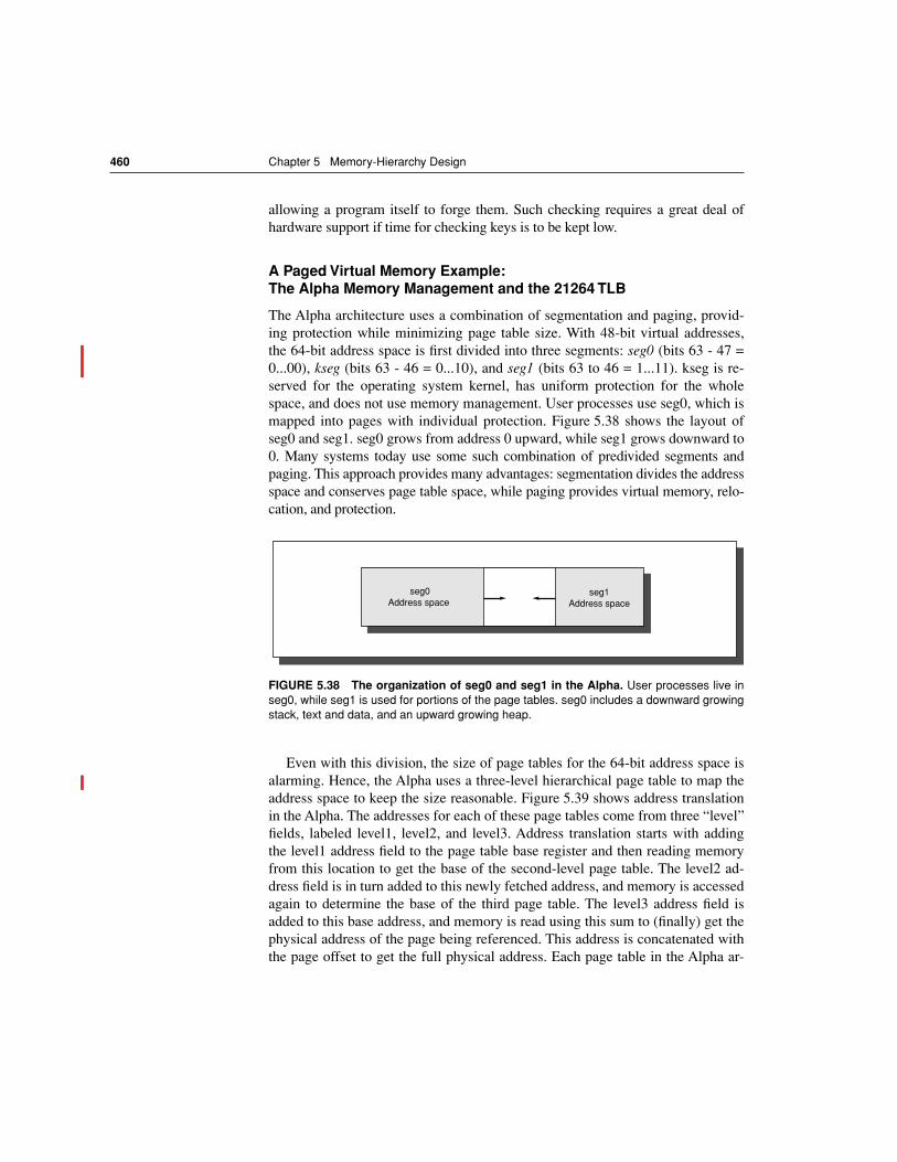
460 Chapter 5 Memory-Hierarchy Design
allowing a program itself to forge them. Such checking requires a great deal ofhardware support if time for checking keys is to be kept low.
A Paged Virtual Memory Example:The Alpha Memory Management and the 21264 TLB
The Alpha architecture uses a combination of segmentation and paging, provid-ing protection while minimizing page table size. With 48-bit virtual addresses,the 64-bit address space is first divided into three segments: seg0 (bits 63 - 47 =0...00), kseg (bits 63 - 46 = 0...10), and seg1 (bits 63 to 46 = 1...11). kseg is re-served for the operating system kernel, has uniform protection for the wholespace, and does not use memory management. User processes use seg0, which ismapped into pages with individual protection. Figure 5.38 shows the layout ofseg0 and seg1. seg0 grows from address 0 upward, while seg1 grows downward to0. Many systems today use some such combination of predivided segments andpaging. This approach provides many advantages: segmentation divides the addressspace and conserves page table space, while paging provides virtual memory, relo-cation, and protection.
Even with this division, the size of page tables for the 64-bit address space isalarming. Hence, the Alpha uses a three-level hierarchical page table to map theaddress space to keep the size reasonable. Figure 5.39 shows address translationin the Alpha. The addresses for each of these page tables come from three “level”fields, labeled level1, level2, and level3. Address translation starts with addingthe level1 address field to the page table base register and then reading memoryfrom this location to get the base of the second-level page table. The level2 ad-dress field is in turn added to this newly fetched address, and memory is accessedagain to determine the base of the third page table. The level3 address field isadded to this base address, and memory is read using this sum to (finally) get thephysical address of the page being referenced. This address is concatenated withthe page offset to get the full physical address. Each page table in the Alpha ar-
FIGURE 5.38 The organization of seg0 and seg1 in the Alpha. User processes live inseg0, while seg1 is used for portions of the page tables. seg0 includes a downward growingstack, text and data, and an upward growing heap.
seg0Address space
seg1Address space
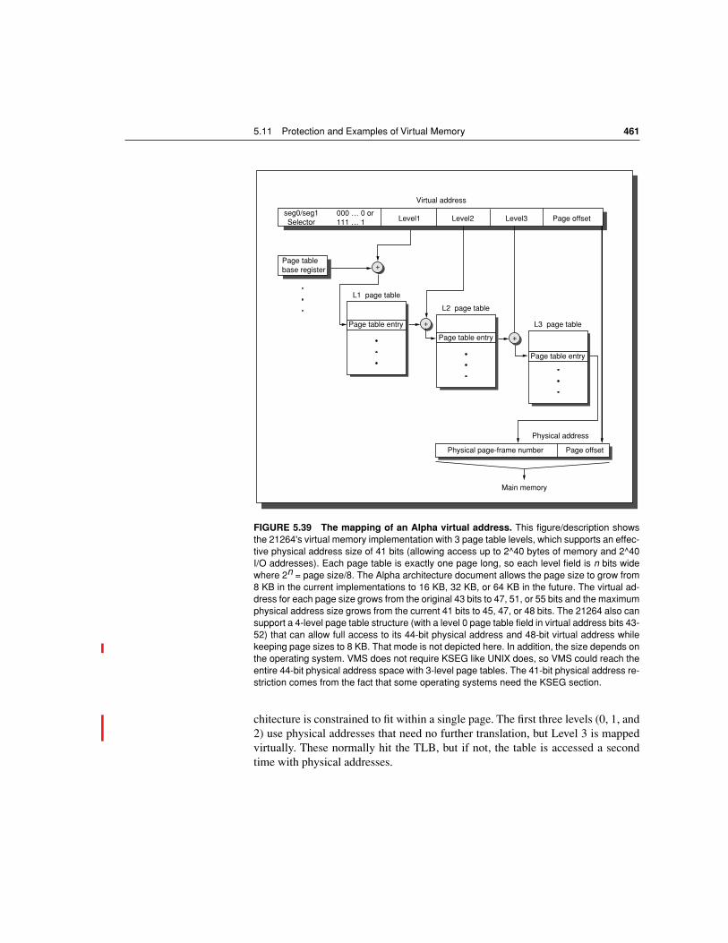
5.11 Protection and Examples of Virtual Memory 461
chitecture is constrained to fit within a single page. The first three levels (0, 1, and2) use physical addresses that need no further translation, but Level 3 is mappedvirtually. These normally hit the TLB, but if not, the table is accessed a secondtime with physical addresses.
FIGURE 5.39 The mapping of an Alpha virtual address. This figure/description showsthe 21264's virtual memory implementation with 3 page table levels, which supports an effec-tive physical address size of 41 bits (allowing access up to 2^40 bytes of memory and 2^40I/O addresses). Each page table is exactly one page long, so each level field is n bits widewhere 2n = page size/8. The Alpha architecture document allows the page size to grow from8 KB in the current implementations to 16 KB, 32 KB, or 64 KB in the future. The virtual ad-dress for each page size grows from the original 43 bits to 47, 51, or 55 bits and the maximumphysical address size grows from the current 41 bits to 45, 47, or 48 bits. The 21264 also cansupport a 4-level page table structure (with a level 0 page table field in virtual address bits 43-52) that can allow full access to its 44-bit physical address and 48-bit virtual address whilekeeping page sizes to 8 KB. That mode is not depicted here. In addition, the size depends onthe operating system. VMS does not require KSEG like UNIX does, so VMS could reach theentire 44-bit physical address space with 3-level page tables. The 41-bit physical address re-striction comes from the fact that some operating systems need the KSEG section.
Page offset
Virtual address
Page table base register +
seg0/seg1Selector
Physical address
Page offsetPhysical page-frame number
Main memory
L1 page table
L2 page table
+ L3 page table
+
Level1 Level2 Level3000 … 0 or111 … 1
Page table entry
Page table entry
Page table entry
462 Chapter 5 Memory-Hierarchy Design
The Alpha uses a 64-bit page table entry (PTE) in each of these page tables.The first 32 bits contain the physical page frame number, and the other halfincludes the following five protection fields:
n Valid—Says that the page frame number is valid for hardware translation
n User read enable—Allows user programs to read data within this page
n Kernel read enable—Allows the kernel to read data within this page
n User write enable—Allows user programs to write data within this page
n Kernel write enable—Allows the kernel to write data within this page
In addition, the PTE has fields reserved for systems software to use as it pleases.Since the Alpha goes through three levels of tables on a TLB miss, there are threepotential places to check protection restrictions. The Alpha obeys only the bot-tom-level PTE, checking the others only to be sure the valid bit is set.
Since the PTEs are 8 bytes long, the page tables are exactly one page long, andthe Alpha 21264 has 8-KB pages, each page table has 1024 PTEs. Each of thethree level fields are 10 bits long and the page offset is 13 bits. This derivationleaves 64 – (3 × 10 + 13) or 21 bits to be defined. If this is a seg0 address, themost-significant bit of the level 1 field is a 0, and for seg1 the two most-signifi-cant bits of the level 1 field are 11two. Alpha requires all bits to the left of thelevel1 field to be identical. For seg0 these 21 bits are all zeros and for seg1 theyare all ones. This restriction means the 21264 virtual addresses are really muchshorter than the full 64 bits found in registers.
The maximum virtual address and physical address is then tied to the pagesize. The original architecture document allows for the Alpha to expand the mini-mum page size from 8 KB up to 64 KB, thereby increasing the virtual address to3 × 13 + 16 or 55 bits and the maximum physical address to 32 + 16 or 48 bits. Infact, the upcoming 21364 supports both. It will be interesting to see whether ornot operating systems accommodate such expansion plans.
Although we have explained translation of legal addresses, what prevents theuser from creating illegal address translations and getting into mischief? Thepage tables themselves are protected from being written by user programs. Thus,the user can try any virtual address, but by controlling the page table entries theoperating system controls what physical memory is accessed. Sharing of memorybetween processes is accomplished by having a page table entry in each addressspace point to the same physical memory page.
The Alpha 21264 employs two TLBs to reduce address translation time, one forinstruction accesses and another for data accesses. Figure 5.40 shows the impor-tant parameters. The Alpha allows the operating system to tell the TLB that con-tiguous sequences of pages can act as one: the options are 8, 64, and 512 timesthe minimum page size. Thus, the variable page size of a PTE mapping makes thematch more challenging, as the size of the space being mapped in the PTE alsomust be checked to determine the match. Figure 5.36 above describes the dataTLB.
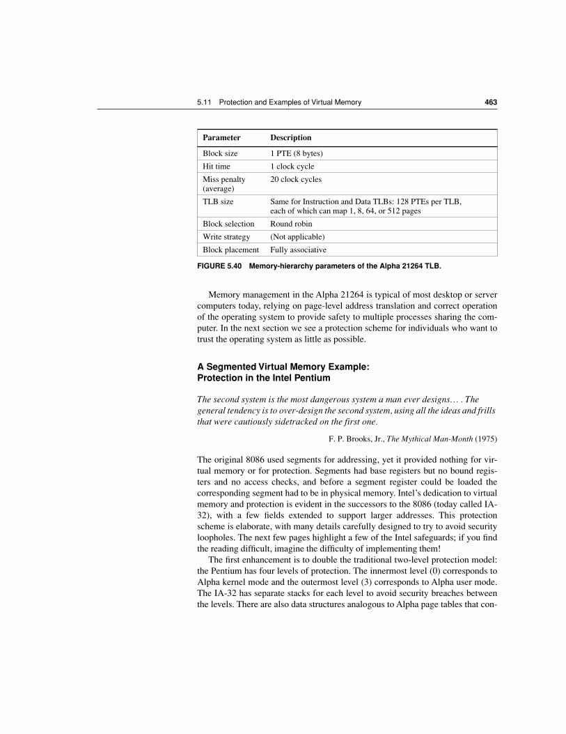
5.11 Protection and Examples of Virtual Memory 463
Memory management in the Alpha 21264 is typical of most desktop or servercomputers today, relying on page-level address translation and correct operationof the operating system to provide safety to multiple processes sharing the com-puter. In the next section we see a protection scheme for individuals who want totrust the operating system as little as possible.
A Segmented Virtual Memory Example: Protection in the Intel Pentium
The second system is the most dangerous system a man ever designs… . The general tendency is to over-design the second system, using all the ideas and frills that were cautiously sidetracked on the first one.
F. P. Brooks, Jr., The Mythical Man-Month (1975)
The original 8086 used segments for addressing, yet it provided nothing for vir-tual memory or for protection. Segments had base registers but no bound regis-ters and no access checks, and before a segment register could be loaded thecorresponding segment had to be in physical memory. Intel’s dedication to virtualmemory and protection is evident in the successors to the 8086 (today called IA-32), with a few fields extended to support larger addresses. This protectionscheme is elaborate, with many details carefully designed to try to avoid securityloopholes. The next few pages highlight a few of the Intel safeguards; if you findthe reading difficult, imagine the difficulty of implementing them!
The first enhancement is to double the traditional two-level protection model:the Pentium has four levels of protection. The innermost level (0) corresponds toAlpha kernel mode and the outermost level (3) corresponds to Alpha user mode.The IA-32 has separate stacks for each level to avoid security breaches betweenthe levels. There are also data structures analogous to Alpha page tables that con-
Parameter Description
Block size 1 PTE (8 bytes)
Hit time 1 clock cycle
Miss penalty (average)
20 clock cycles
TLB size Same for Instruction and Data TLBs: 128 PTEs per TLB, each of which can map 1, 8, 64, or 512 pages
Block selection Round robin
Write strategy (Not applicable)
Block placement Fully associative
FIGURE 5.40 Memory-hierarchy parameters of the Alpha 21264 TLB.
464 Chapter 5 Memory-Hierarchy Design
tain the physical addresses for segments, as well as a list of checks to be made ontranslated addresses.
The Intel designers did not stop there. The IA-32 divides the address space, al-lowing both the operating system and the user access to the full space. The IA-32user can call an operating system routine in this space and even pass parametersto it while retaining full protection. This safe call is not a trivial action, since thestack for the operating system is different from the user’s stack. Moreover, theIA-32 allows the operating system to maintain the protection level of the calledroutine for the parameters that are passed to it. This potential loophole in protec-tion is prevented by not allowing the user process to ask the operating system toaccess something indirectly that it would not have been able to access itself.(Such security loopholes are called Trojan horses.)
The Intel designers were guided by the principle of trusting the operating sys-tem as little as possible, while supporting sharing and protection. As an exampleof the use of such protected sharing, suppose a payroll program writes checks andalso updates the year-to-date information on total salary and benefits payments.Thus, we want to give the program the ability to read the salary and year-to-dateinformation, and modify the year-to-date information but not the salary. We shallsee the mechanism to support such features shortly. In the rest of this subsection,we will look at the big picture of the IA-32 protection and examine its motiva-tion.
Adding Bounds Checking and Memory MappingThe first step in enhancing the Intel processor was getting the segmented address-ing to check bounds as well as supply a base. Rather than a base address, as in the8086, segment registers in the IA-32 contain an index to a virtual memory datastructure called a descriptor table. Descriptor tables play the role of page tablesin the Alpha. On the IA-32 the equivalent of a page table entry is a segmentdescriptor. It contains fields found in PTEs:
n A present bit—equivalent to the PTE valid bit, used to indicate this is a validtranslation
n A base field—equivalent to a page frame address, containing the physicaladdress of the first byte of the segment
n An access bit—like the reference bit or use bit in some architectures that ishelpful for replacement algorithms
n An attributes field—specifies the valid operations and protection levels foroperations that use this segment
There is also a limit field, not found in paged systems, which establishes theupper bound of valid offsets for this segment. Figure 5.41 shows examples of IA-32 segment descriptors.
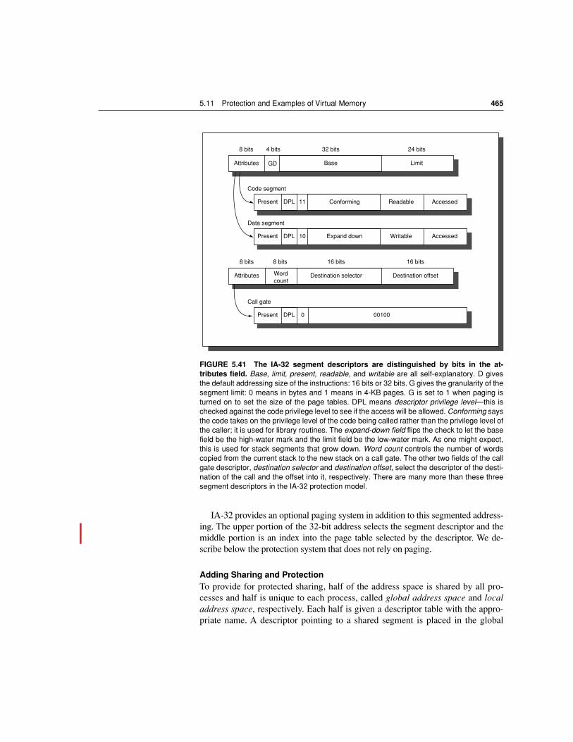
5.11 Protection and Examples of Virtual Memory 465
IA-32 provides an optional paging system in addition to this segmented address-ing. The upper portion of the 32-bit address selects the segment descriptor and themiddle portion is an index into the page table selected by the descriptor. We de-scribe below the protection system that does not rely on paging.
Adding Sharing and ProtectionTo provide for protected sharing, half of the address space is shared by all pro-cesses and half is unique to each process, called global address space and localaddress space, respectively. Each half is given a descriptor table with the appro-priate name. A descriptor pointing to a shared segment is placed in the global
FIGURE 5.41 The IA-32 segment descriptors are distinguished by bits in the at-tributes field. Base, limit, present, readable, and writable are all self-explanatory. D givesthe default addressing size of the instructions: 16 bits or 32 bits. G gives the granularity of thesegment limit: 0 means in bytes and 1 means in 4-KB pages. G is set to 1 when paging isturned on to set the size of the page tables. DPL means descriptor privilege level—this ischecked against the code privilege level to see if the access will be allowed. Conforming saysthe code takes on the privilege level of the code being called rather than the privilege level ofthe caller; it is used for library routines. The expand-down field flips the check to let the basefield be the high-water mark and the limit field be the low-water mark. As one might expect,this is used for stack segments that grow down. Word count controls the number of wordscopied from the current stack to the new stack on a call gate. The other two fields of the callgate descriptor, destination selector and destination offset, select the descriptor of the desti-nation of the call and the offset into it, respectively. There are many more than these threesegment descriptors in the IA-32 protection model.
Attributes Base Limit
8 bits 4 bits 32 bits 24 bits
Present
Code segment
DPL 11 Conforming Readable Accessed
Present
Data segment
DPL 10 Expand down Writable Accessed
Attributes Destination selector Destination offset
8 bits 16 bits 16 bits
Wordcount
8 bits
Present
Call gate
DPL 0 00100
GD
466 Chapter 5 Memory-Hierarchy Design
descriptor table, while a descriptor for a private segment is placed in the localdescriptor table.
A program loads a IA-32 segment register with an index to the table and a bitsaying which table it desires. The operation is checked according to the attributesin the descriptor, the physical address being formed by adding the offset in theCPU to the base in the descriptor, provided the offset is less than the limit field.Every segment descriptor has a separate 2-bit field to give the legal access levelof this segment. A violation occurs only if the program tries to use a segmentwith a lower protection level in the segment descriptor.
We can now show how to invoke the payroll program mentioned above to up-date the year-to-date information without allowing it to update salaries. The pro-gram could be given a descriptor to the information that has the writable fieldclear, meaning it can read but not write the data. A trusted program can then besupplied that will only write the year-to-date information. It is given a descriptorwith the writable field set (Figure 5.41). The payroll program invokes the trustedcode using a code segment descriptor with the conforming field set. This settingmeans the called program takes on the privilege level of the code being calledrather than the privilege level of the caller. Hence, the payroll program can readthe salaries and call a trusted program to update the year-to-date totals, yet thepayroll program cannot modify the salaries. If a Trojan horse exists in this sys-tem, to be effective it must be located in the trusted code whose only job is to up-date the year-to-date information. The argument for this style of protection is thatlimiting the scope of the vulnerability enhances security.
Adding Safe Calls from User to OS Gates and Inheriting Protection Level for ParametersAllowing the user to jump into the operating system is a bold step. How, then, cana hardware designer increase the chances of a safe system without trusting theoperating system or any other piece of code? The IA-32 approach is to restrictwhere the user can enter a piece of code, to safely place parameters on the properstack, and to make sure the user parameters don’t get the protection level of thecalled code.
To restrict entry into others’ code, the IA-32 provides a special segmentdescriptor, or call gate, identified by a bit in the attributes field. Unlike other de-scriptors, call gates are full physical addresses of an object in memory; the offsetsupplied by the CPU is ignored. As stated above, their purpose is to prevent theuser from randomly jumping anywhere into a protected or more-privileged codesegment. In our programming example, this means the only place the payroll pro-gram can invoke the trusted code is at the proper boundary. This restriction isneeded to make conforming segments work as intended.
What happens if caller and callee are “mutually suspicious,” so that neithertrusts the other? The solution is found in the word count field in the bottom de-scriptor in Figure 5.41. When a call instruction invokes a call gate descriptor, thedescriptor copies the number of words specified in the descriptor from the local
5.12 Crosscutting Issues in the Design of Memory Hierarchies 467
stack onto the stack corresponding to the level of this segment. This copying al-lows the user to pass parameters by first pushing them onto the local stack. Thehardware then safely transfers them onto the correct stack. A return from a callgate will pop the parameters off both stacks and copy any return values to theproper stack. Note that this model is incompatible with the current practice ofpassing parameters in registers.
This scheme still leaves open the potential loophole of having the operatingsystem use the user’s address, passed as parameters, with the operating system’ssecurity level, instead of with the user’s level. The IA-32 solves this problem bydedicating 2 bits in every CPU segment register to the requested protection level.When an operating system routine is invoked, it can execute an instruction thatsets this 2-bit field in all address parameters with the protection level of the userthat called the routine. Thus, when these address parameters are loaded into thesegment registers, they will set the requested protection level to the proper value.The IA-32 hardware then uses the requested protection level to prevent any fool-ishness: No segment can be accessed from the system routine using those param-eters if it has a more-privileged protection level than requested.
Summary: Protection on the Alpha versus the IA-32
If the IA-32 protection model looks harder to build than the Alpha model, that’sbecause it is. This effort must be especially frustrating for the IA-32 engineers,since few customers use the elaborate protection mechanism. In addition, the factthat the protection model is a mismatch for the simple paging protection ofUNIX-like systems means it will be used only by someone writing an operatingsystem especially for this computer.
In the last edition we wondered whether the popularity of the Internet wouldlead to demands for increased support for security, and hence put this elaborateprotection model to good use. Despite widely documented security breaches andthe ubiquity of this architecture, no one has proposed a new operating system toleverage the 80x86 protection features.
This section describes four topics discussed in other chapters that are fundamen-tal to memory-hierarchy design.
Superscalar CPU and Number of Ports to the Cache
One complexity of the advanced designs of Chapters 3 and 4 is that multiple in-structions can be issued within a single clock cycle. Clearly, if there is not suffi-cient peak bandwidth from the cache to match the peak demands of theinstructions, there is little benefit to designing such parallelism in the processor.
5.12 Crosscutting Issues in the Design of Memory Hierarchies
468 Chapter 5 Memory-Hierarchy Design
Some processors increase complexity of instruction fetch by allowing instruc-tions to be issued to be found on any boundary instead of, say, a multiple of fourwords. As mentioned above, similar reasoning applies to CPUs that want to con-tinue executing instructions on a cache miss: clearly the memory hierarchy mustalso be nonblocking or the CPU cannot benefit.
For example, the UltraSPARC III fetches up to 4 instructions per clock cycle,and executes up to 4, with up to 2 being loads or stores. Hence, the instructioncache must deliver 128 bits per clock cycle and the data cache must support two64-bit accesses per clock cycle.
Speculative Execution and the Memory System
Inherent in CPUs that support speculative execution or conditional instructions isthe possibility of generating invalid addresses that would not occur without spec-ulative execution. Not only would this be incorrect behavior if exceptions weretaken, the benefits of speculative execution would be swamped by false exceptionoverhead. Hence, the memory system must identify speculatively executed in-structions and conditionally executed instructions and suppress the correspond-ing exception.
By similar reasoning, we cannot allow such instructions to cause the cache tostall on a miss, for again unnecessary stalls could overwhelm the benefits ofspeculation. Hence, these CPUs must be matched with nonblocking caches (seepage 421).
In reality, the penalty of the an L2 miss is so large that compilers normallyonly speculate on L1 misses. Figure 5.23 on page 423 shows that for some well-behaved scientific programs the compiler can sustain multiple outstanding L2misses (“miss under miss”) so as to effectively cut the L2 miss penalty. Onceagain, for this to work the memory system behind the cache must match the de-sires of the compiler in number of simultaneous memory accesses.
Combining the Instruction Cache with Instruction Fetch and Decode Mechanisms
With Moore’s Law continuing to offer more transistors and increasing demandsfor instruction level parallelism and clock rate, increasingly the instruction cacheand first part of instruction execution are merging (see Chapter 3).
The leading example is the Netburst microarchitecture of the Pentium 4 andits successors. Not only does it use a trace cache (see page 434), which combinesbranch prediction with instruction fetch, it stores the internal RISC operations(see Chapter 3) in the trace cache. Hence, cache hits save 5 of 25 pipeline stagesfor decoding and translation. The downside of caching decoded instructions isimpact on die size. It appears on the die that the 12000 RISC operations in thetrace cache take equivalent of 96 KB of SRAM, which suggests that the RISC op-erations are about 64-bits long. 80x86 instructions would surely be two to threetimes more efficient.
5.12 Crosscutting Issues in the Design of Memory Hierarchies 469
Embedded computers also have bigger instructions in the cache, but for anoth-er reason. Given the importance of code size for such applications, several keep acompressed version of the instruction in main memory and then expand to thefull size in the instruction cache (see page 130 in Chapter 2.)
Embedded Computer Caches and Real Time Performance
As mentioned before, embedded computers often are placed in real time environ-ments where a set of tasks must be completed every time period. In such situa-tions performance variability is of more concern than average case performance.Since caches were invented to improve average case performance at the cost ofgreater variability, they would seem to be a problem for real time computing.
In practice, instruction caches are widely used in embedded computers sincemost code has predictable behavior. Data caches then are the real issue.
To cope with that challenge, some embedded computers allow a portion of thecache to be “locked down.” That is, a portion of the cache acts like a smallscratchpad memory under program control. In a set associative data cache, oneblock of an entry would be locked down while the others could still buffer access-es to main memory. If it was direct mapped, then every address that maps ontothat locked down block would result in a miss and later is passed to the CPU.
Embedded Computer Caches and Power
Although caches were invented to reduce memory access time, they also savepower. It is much more power efficient to access on chip memory than it is todrive the pins of the chip, drive the memory bus, activate the external memorychips and then make the return trip.
To further improve power efficiency of caches on chip, some of the optimiza-tions in sections 5.4 to 5.7 are reoriented for power. For example, the MIPS 4300uses way prediction to only power half of the address checking hardware for itstwo-way set associative cache.
I/O and Consistency of Cached Data
Because of caches, data can be found in memory and in the cache. As long as theCPU is the sole device changing or reading the data and the cache stands betweenthe CPU and memory, there is little danger in the CPU seeing the old or stalecopy. I/O devices give the opportunity for other devices to cause copies to be in-consistent or for other devices to read the stale copies. Figure 5.42 illustrates theproblem, generally referred to as the cache-coherency problem.
The question is this: Where does the I/O occur in the computer—between theI/O device and the cache or between the I/O device and main memory? If inputputs data into the cache and output reads data from the cache, both I/O and theCPU see the same data, and the problem is solved. The difficulty in this approach
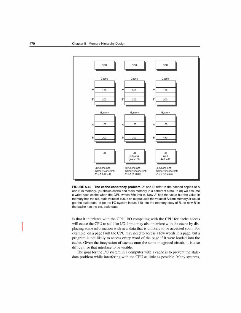
470 Chapter 5 Memory-Hierarchy Design
is that it interferes with the CPU. I/O competing with the CPU for cache accesswill cause the CPU to stall for I/O. Input may also interfere with the cache by dis-placing some information with new data that is unlikely to be accessed soon. Forexample, on a page fault the CPU may need to access a few words in a page, but aprogram is not likely to access every word of the page if it were loaded into thecache. Given the integration of caches onto the same integrated circuit, it is alsodifficult for that interface to be visible.
The goal for the I/O system in a computer with a cache is to prevent the stale-data problem while interfering with the CPU as little as possible. Many systems,
FIGURE 5.42 The cache-coherency problem. A' and B' refer to the cached copies of Aand B in memory. (a) shows cache and main memory in a coherent state. In (b) we assumea write-back cache when the CPU writes 550 into A. Now A' has the value but the value inmemory has the old, stale value of 100. If an output used the value of A from memory, it wouldget the stale data. In (c) the I/O system inputs 440 into the memory copy of B, so now B' inthe cache has the old, stale data.
CPU CPU CPU
100
200
A'
B'
B
A
Cache Cache Cache
Memory Memory Memory
550
200
A'
B'
200
I/Ooutput Agives 100
B
A
100
100 100 100
200
A'
B'
440
I/Oinput
440 to B
(a) Cache andmemory coherent:A' = A & B' = B
(b) Cache andmemory incoherent:A' ≠ A (A stale)
(c) Cache andmemory incoherent:B' ≠ B (B' stale)
B
A
I/O
200
5.13 Putting It All Together: Alpha 21264 Memory Hierarchy 471
therefore, prefer that I/O occur directly to main memory, with main memoryacting as an I/O buffer. If a write-through cache were used, then memory wouldhave an up-to-date copy of the information, and there would be no stale-data is-sue for output. (This benefit is a reason processors used write through.) Alas,write-through usually found only today in first level data caches backed by a L2cache which uses write back. Even embedded caches avoid write through for rea-sons of power efficiency
Input requires some extra work. The software solution is to guarantee that noblocks of the I/O buffer designated for input are in the cache. In one approach, abuffer page is marked as noncachable; the operating system always inputs to sucha page. In another approach, the operating system flushes the buffer addressesfrom the cache after the input occurs. A hardware solution is to check the I/O ad-dresses on input to see if they are in the cache. To avoid slowing down the cacheto check addresses, a duplicate set of tags may be used to allow checking of I/Oaddresses in parallel with processor cache accesses. If there is a match of I/O ad-dresses in the cache, the cache entries are invalidated to avoid stale data. All theseapproaches can also be used for output with write-back caches. More about this isfound in Chapter 7.
The cache-coherency problem applies to multiprocessors as well as I/O. Un-like I/O, where multiple data copies are a rare event—one to be avoided when-ever possible—a program running on multiple processors will want to havecopies of the same data in several caches. Performance of a multiprocessor pro-gram depends on the performance of the system when sharing data. The proto-cols to maintain coherency for multiple processors are called cache-coherencyprotocols, and are described in Chapter 6.
Thus far we have given glimpses of the Alpha 21264 memory hierarchy; this sec-tion unveils the full design and shows the performance of its components for theSPEC95 programs. Figure 5.43 gives the overall picture of this design. The21264 is an out-of-order execution processor that fetches up to four instructionsper clock cycle and executes up to six instructions per clock cycle. It uses either a48-bit virtual address and a 44-bit physical address or 43-bit virtual address and41-bit physical; thus far, all systems just use 41 bits. In either case, Alpha halvesthe physical address space, with the lower half for memory addresses and the up-per half for I/O addresses. For the rest of this section, we assume use of the 43-bitvirtual address and the 41-bit physical address.
Let's really start at the beginning, when the Alpha is turned on. Hardware onthe chip loads the instruction cache serially from an external PROM. This initial-ization fills up to 64-KB worth of instructions (16K instructions) into the cache.The same serial interface (and PROM) also loads configuration information thatspecifies L2 cache speed/timing, system port speed/timing, and much other infor-
5.13 Putting It All Together: Alpha 21264 Memory Hierarchy
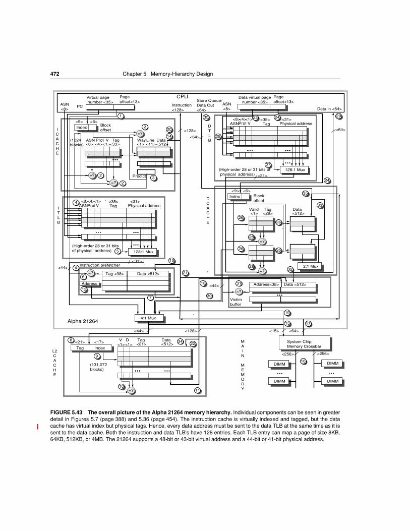
472 Chapter 5 Memory-Hierarchy Design
FIGURE 5.43 The overall picture of the Alpha 21264 memory hierarchy. Individual components can be seen in greaterdetail in Figures 5.7 (page 388) and 5.36 (page 454). The instruction cache is virtually indexed and tagged, but the datacache has virtual index but physical tags. Hence, every data address must be sent to the data TLB at the same time as it issent to the data cache. Both the instruction and data TLB's have 128 entries. Each TLB entry can map a page of size 8KB,64KB, 512KB, or 4MB. The 21264 supports a 48-bit or 43-bit virtual address and a 44-bit or 41-bit physical address.
System ChipMemory Crossbar
Victim buffer
6
7
12
13
14
20
23
25
24
24
26
26
27
28
26
2935
35
33
32
31
34
30
Virtual page number <35>
Instruction <128> Data in <64>
Store Queue/Data Out <64>
<128>
<64>
<44>
<128>
<256> <256>
<44> <15> <64>
<44>
<64>
Pageoffset<13>
Blockoffset
Index
<9> <6>
Data virtual page number <35>
V Physical address<8> <31>
ASN<4>Prot
<1>Tag
<35>
<31>
(High-order 28 or 31 bits of physical address)
Pageoffset<13>
DCACHE
DTLB
PC
CPU
Alpha 21264
=?
Instruction prefetcher
Tag <38> Data <512>
=?
Address<38> Data <512>
Valid Data<1> <29> <512>
=?
Tag
Blockoffset
Index
<9> <6>
ICACHE
Way<33> <1>
Line<11>
Data<512>
2
2
2
4
4
8
1
3
(1024blocks)
Tag<4>Prot
<1>V
<8>ASN
ASN<8>
ASN<8>
=?
=?
=?
<31>
5
ASN Physical address<8> <31>
Prot<4>
V<1>
Tag<35>
(High-order 28 or 31 bits of physical address)
ITLB
128:1 Mux
4:1 Mux
DIMM
DIMM DIMM
2:1 Mux
128:1 Mux
V Data<1>
D<1> <21> <512>
=?
(131,072blocks)
<21>
Tag Index
<17> Tag
Address
9
1011
22
15
16
17
19
18
21
L2CACHE
MAIN
MEMORY
28
26
=?
Predict
DIMM
5.13 Putting It All Together: Alpha 21264 Memory Hierarchy 473
mation necessary for the 21264 to communicate with the external logic. Thiscode completes the remainder of the processor and system initialization.
The preloaded instructions execute in Privileged Architecture Library (PAL)mode. The software executed in PAL mode is simply machine language routineswith some implementation-specific extensions to allow access to low-level hard-ware, such as the TLB. PAL code runs with exceptions disabled, and the instruc-tion addresses are not translated. Since PAL code avoids the TLB, instructionaccesses are not checked for memory management violations.
One of the first steps is to update the instruction TLB with valid page table en-tries (PTEs) for this process. Kernel code updates the appropriate page table en-try (in memory) for each page to be mapped. A miss in the TLB is handled byPAL code, since normal code that relies on the TLB cannot change the TLB.
Once the operating system is ready to begin executing a user process, it setsthe PC to the appropriate address in segment seg0.
We are now ready to follow memory hierarchy in action: Figure 5.43 is la-beled with the steps of this narrative. First, a 12-bit address is sent to the 64-KBinstruction cache, along with a 35-bit page number. An 8-bit Address SpaceNumber (ASN) is also sent, for the same purpose as using ASN’s in the TLB(step 1).The instruction cache is virtually indexed and virtually tagged, so in-struction TLB translations are only required on cache misses. As mentioned insection 5.5, the Instruction cache uses way prediction, so a 1-bit way predict bit isprepended to the 9-bit index. The effective index is then 10 bits, similar to a 64-KB direct mapped cache with 1024 blocks. Thus, the effective instruction cacheindex is 10 bits (see page 387), and the instruction cache tag is then 48 – 9 bits(actual index) – 6 bits (block offset) or 33 bits. As the 21264 expects 4 instruc-tions (16 bytes) each instruction fetch, an additional 2 bits is used from the 6-bitblock offset to select the appropriate 16 bytes. Hence, 10 + 2 or 12 bits to read 16bytes of instructions.
To reduce latency, the instruction cache includes two mechanisms to beginearly access of the next block. As mentioned in section 5.5, the way predictingcache relies on a 1-bit field for every 16 bytes to predict which of two sets will beused next, offering the hit time of direct mapped with miss rate of two-way asso-ciativity. It also includes 11 bits to predict the next group of 16 bytes to be read.This field is loaded with the address of the next sequential group on a cache miss,and updated to a nonsequential address by the dynamic branch predictor. Thesetwo techniques are called way prediction and line prediction.
Thus, the index field of the PC is compared to the predicted block address, thetag field of the PC is compared to the address from the tag portion of the cache,and the 8-bit process ASN to the tag ASN field (step 2). The valid bit is alsochecked. If any field has the wrong value, it is a miss. On a hit in the instructioncache, the proper fetch block is supplied, and the next way and line prediction isloaded to read the next block (step 3). There is also a protection field in the tag, to
474 Chapter 5 Memory-Hierarchy Design
ensure that instruction fetch does not violate protection barriers. The instructionstream access is now done.
An instruction cache miss causes a simultaneous check of the instruction TLBand the instruction prefetcher (step 4). The fully associative TLB simultaneouslysearches all 128 entries to find a match between the address and a valid PTE (step5). In addition to translating the address, the TLB checks to see if the PTE de-mands that this access result in an exception, and if the address space number ofthe processor matches the address space number in the field. An exception mightoccur if either this access violates the protection on the page or if the page is notin main memory. If the desired instruction address is found in the instructionprefetcher (step 6), the instructions are (eventually) supplied directly by theprefetcher (step 7). Otherwise, if there is no TLB exception, an access to the sec-ond-level cache is started (step 8).
In the case of a complete miss, the second-level cache continues trying tofetch the block. The 21264 microprocessor is designed to work with direct-mapped second-level caches from 1MB to 16 MB. For this section we use thememory system of the 667 Mhz Compaq AlphaserverES40, a shared memorysystem with from 1 to 4 processors. It has a 444 Mhz, 8-MB direct-mapped, sec-ond-level cache. (The data rate is 444 Mhz; the L2 SRAM parts use the doubledata rate technique of DRAMs, so they are clocked at only half that rate.)The L2index is
so the 35-bit block address (41-bit physical address – 6-bit block offset) is divid-ed into a 18-bit tag and a 17-bit index (step 9).The cache controller reads the tagfrom that index and if it matches and is valid (step 10), it returns the critical 16bytes (step 11), with the remaining 48 bytes of the cache block supplied 16 bytesper 2.25 ns. The 21264 L2 interface does not require that the L2 cache clock bean integer multiple of the processor clock, so it can be loaded faster than 3.00 nsthat you might expect from a 667 MHz processor. At the same time, a request ismade for the next sequential 64-byte block (step 12), which is loaded into the in-struction prefetcher in the next 6 clock cycles (step 13). Each miss can cause aprefetch of up to 4 cache blocks. An instruction cache miss costs approximately15 CPU cycles (22 ns), depending on clock alignments.
By the way, the instruction prefetcher does not rely on the TLB for addresstranslation. It simply increments the physical address of the miss by 64 bytes,checking to make sure that the new address is within the same page. If the incre-mented address crosses a page boundary, then the prefetch is suppressed. To savetime, the prefetched instructions are passed around the CPU and then written tothe instruction cache while the instructions execute in the CPU (step 14).
If the instruction is not found in the secondary cache, the physical addresscommand is sent to the ES40 system chip set via four consecutive transfer cycles
2index Cache size
Block size Set associativity×----------------------------------------------------------------------8192K64 1×----------------
128K 217
= = ==
5.13 Putting It All Together: Alpha 21264 Memory Hierarchy 475
on a narrow, 15-bit outbound address bus (step 15). The address and commanduse the address bus for 8 CPU cycles. The ES40 connects the microprocessor tomemory via a crossbar to one of two 256-bit memory busses to service the re-quest (step 16). Each bus contains a variable number of DIMMs (dual inlinememory modules). The size and number of DIMMs can vary to give a total of 32GB of memory in the 667 Mhz ES40. Since the 21264 provides single error cor-rection/double error detection checking on data cache (see section 5.15), L2cache, busses, and main memory, the data busses actually include an additional32-bits for ECC bits.
Although the crossbar has two 256-bit buses, the path to the microprocessor ismuch narrower. 64 data bits. Thus, the 21264 has two off-chip paths: 128 databits for the L2 cache and 64 data bits for memory crossbar. Separate paths allowsa point-to-point connection and hence a high clock rate interface for both the L2cache and the crossbar.
The total latency of the instruction miss that is serviced by main memory isapproximately 130 CPU cycles for the critical instructions. The system logic fillsthe remainder of the 64-byte cache block at a rate of 8 bytes per 2 CPU cycles(step 17).
Since the second-level cache is a write-back cache, any miss can lead to an oldblock being written back to memory. The 21264 places this “victim” block into avictim file (step 18), as it does with a victim dirty block in the data cache, to getout of the way of new data when the new cache reference determined first readthe L2 cache; that is, the original instruction fetch read that missed (step 8). The21264 sends out the address of the victim out the system address bus followingthe address of the new request (step 19). The system chip set later extracts thevictim data and writes it to the memory DIMMs.
The new data are loaded into the instruction cache as soon as they arrive (step20). It also goes into a (L1) victim buffer (step 21), and is later written to the L2cache (step 22). The victim buffer is of size 8, so many victims can be queued be-fore being written back either to the L2 or to memory. The 21264 can also man-age up to 8 simultaneous cache block misses, allowing it to hit under 8 misses asdescribed in section 5.4.
If this initial instruction is a load, the data addresses is also sent to the datacache. It is 64 KB, 2-way set-associative, and write-back with a 64-byte blocksize. Unlike the instruction cache, the data cache is virtually indexed and physi-cally tagged. Thus, the page frame of the instruction’s data address is sent to thedata TLB (step 23) at the same time as the (9+3)-bit index from the virtual ad-dress is sent to the data cache (step 24). The data TLB is a fully associative cachecontaining 128 PTEs (step 25), each of which represents page sizes from 8 KB to4 MB. A TLB miss will trap to PAL code to load the valid PTE for this address.In the worst case, the page is not in memory, and the operating system gets thepage from disk, just as before. Since millions of instructions could execute duringa page fault, the operating system will swap in another process if one is waitingto run.
476 Chapter 5 Memory-Hierarchy Design
The index field of the address is sent of both sets of the data cache (step 26).Assuming that we have a valid PTE in the data TLB (step 27), the two tags andvalid bits are compared to the physical page frame (step 28), with a match send-ing the desired 8 bytes to the CPU (step 29). A miss goes to the second-levelcache, which proceeds similar to an instruction miss (Step 30), except that it mustcheck the victim buffer first to be sure the block is not there (Step 31).
As mentioned in section 5.7, the data cache can be virtually addressed andphysically tagged. On a miss, the cache controller must check for a synonym(two different virtual addresses that reference the same physical address). Hence,the data cache tags are examined in parallel with the L2 cache tags during an L2lookup. As the minimum page size is 8 KB or 13 bits and the cache index plusblock offset is 15 bits, the cache must check 22 or 4 blocks per set for synonyms.If it finds a synonym, the offending block is invalidated. This guarantees that acache block can reside in one of the 8 possible data cache locations at any giventime.
A write back victim can be produced on a data cache miss. The victim data isextracted from the data cache simultaneously with the fill of the data cache withthe L2 data, and sent to the victim buffer (Step 32). I
In the case of an L2 miss, the fill data from the system is written directly intothe (L1) data cache (step 33). The L2 is written only with L1 victims (step 34).They appear either because they were modified by the CPU, or because they hadbeen loaded from memory directly into the data cache but not yet written into theL2 cache.
Suppose the instruction is a store instead of a load. When the store issues itdoes a data cache lookup just like a load. A store miss causes the block to befilled into the data cache very much as with a load miss. The store does not up-date the cache until later, after it is known to be non-speculative. During this timethe store resides in a store queue, part of the out-of-order control mechanism ofthe CPU. Stores write from the store queue into the data cache on idle cache cy-cles (step 35). The data cache is ECC protected, so a read-modify-write operationis required to update the data cache on stores.
Performance of the 21264 Memory Hierarchy
How well does the 21264 work? The bottom line in this evaluation is the per-centage of time lost while the CPU is waiting for the memory hierarchy. The ma-jor components are the instruction and data caches, instruction and data TLBs,and the secondary cache. Alas, in an out-of-order execution processors like the21264 it is very hard to isolate the time waiting for memory, since a memory stallfor one instruction may be completely hidden by successful completion of a laterinstruction.
How well does out-or-order perform compared in in-order? Figure 5.44 showsrelative performance for SPECint2000 benchmarks for the out-of-order 21264and its predecessor, the in-order Alpha 21164. The clock rates are similar in the
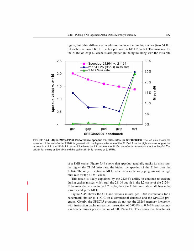
5.13 Putting It All Together: Alpha 21264 Memory Hierarchy 477
figure, but other differences in addition include the on-chip caches (two 64 KBL1 caches vs. two 8 KB L1 caches plus one 96 KB L2 cache). The miss rate forthe 21164 on-chip L2 cache is also plotted in the figure along with the miss rate
of a 1MB cache. Figure 5.44 shows that speedup generally tracks its miss rate;the higher the 21164 miss rate, the higher the speedup of the 21264 over the21164. The only exception is MCF, which is also the only program with a highmiss rate for the a 1MB cache.
This result is likely explained by the 21264’s ability to continue to executeduring caches misses which stall the 21164 but hit in the L2 cache of the 21264.If the miss also misses in the L2 cache, then the 21264 must also stall, hence thelower speedup for MCF.
Figure 5.45 shows the CPI and various misses per 1000 instructions for abenchmark similar to TPC-C on a commercial database and the SPEC95 pro-grams. Clearly, the SPEC95 programs do not tax the 21264 memory hierarchy,with instruction cache misses per instruction of 0.001% to 0.343% and second-level cache misses per instruction of 0.001% to 1%. The commercial benchmark
FIGURE 5.44 Alpha 21264/21164 Performance speedup vs. miss rates for SPECint2000. The left axis shows thespeedup of the out-of-order 21264 is greatest with the highest miss rate of the 21164 L2 cache (right axis) as long as theaccess is a hit in the 21264 L2 cache. If it misses the L2 cache of the 21264, out-of-order execution is not as helpful. The21264 is running at 500 MHz and the earlier 21164 is running at 533MHz.
-
0.5
1.0
1.5
2.0
2.5
gcc gap perl gzip mcf
SPECint2000 benchmark
Sp
eed
up
212
64 v
. 21
164
0%
5%
10%
15%
20%
25%
30%
Mis
s ra
te
Speedup 21264 v. 2116421164 L2$ (96KB) miss rate1 MB Miss rate
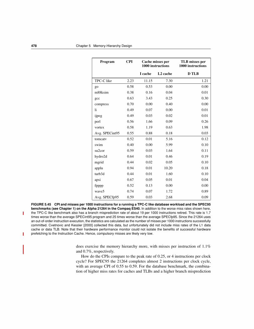
478 Chapter 5 Memory-Hierarchy Design
does exercise the memory hierarchy more, with misses per instruction of 1.1%and 0.7%, respectively.
How do the CPIs compare to the peak rate of 0.25, or 4 instructions per clockcycle? For SPEC95 the 21264 completes almost 2 instructions per clock cycle,with an average CPI of 0.55 to 0.59. For the database benchmark, the combina-tion of higher miss rates for caches and TLBs and a higher branch misprediction
Program CPI Cache misses per 1000 instructions
TLB misses per 1000 instructions
I cache L2 cache D TLB
TPC-C like 2.23 11.15 7.30 1.21
go 0.58 0.53 0.00 0.00
m88ksim 0.38 0.16 0.04 0.01
gcc 0.63 3.43 0.25 0.30
compress 0.70 0.00 0.40 0.00
li 0.49 0.07 0.00 0.01
ijpeg 0.49 0.03 0.02 0.01
perl 0.56 1.66 0.09 0.26
vortex 0.58 1.19 0.63 1.98
Avg. SPECint95 0.55 0.88 0.18 0.03
tomcatv 0.52 0.01 5.16 0.12
swim 0.40 0.00 5.99 0.10
su2cor 0.59 0.03 1.64 0.11
hydro2d 0.64 0.01 0.46 0.19
mgrid 0.44 0.02 0.05 0.10
applu 0.94 0.01 10.20 0.18
turb3d 0.44 0.01 1.60 0.10
apsi 0.67 0.05 0.01 0.04
fpppp 0.52 0.13 0.00 0.00
wave5 0.74 0.07 1.72 0.89
Avg. SPECfp95 0.59 0.03 2.68 0.09
FIGURE 5.45 CPI and misses per 1000 instructions for a running a TPC-C like database workload and the SPEC95benchmarks (see Chapter 1) on the Alpha 21264 in the Compaq ES40. In addition to the worse miss rates shown here,the TPC-C like benchmark also has a branch misprediction rate of about 19 per 1000 instructions retired. This rate is 1.7times worse than the average SPECint95 program and 25 times worse than the average SPECfp95. Since the 21264 usesan out-of-order instruction execution, the statistics are calculated as the number of misses per 1000 instructions successfullycommitted. Cvetnovic and Kessler [2000] collected this data, but unfortunately did not include miss rates of the L1 datacache or data TLB. Note that their hardware performance monitor could not isolate the benefits of successful hardwareprefetching to the Instruction Cache. Hence, compulsory misses are likely very low.
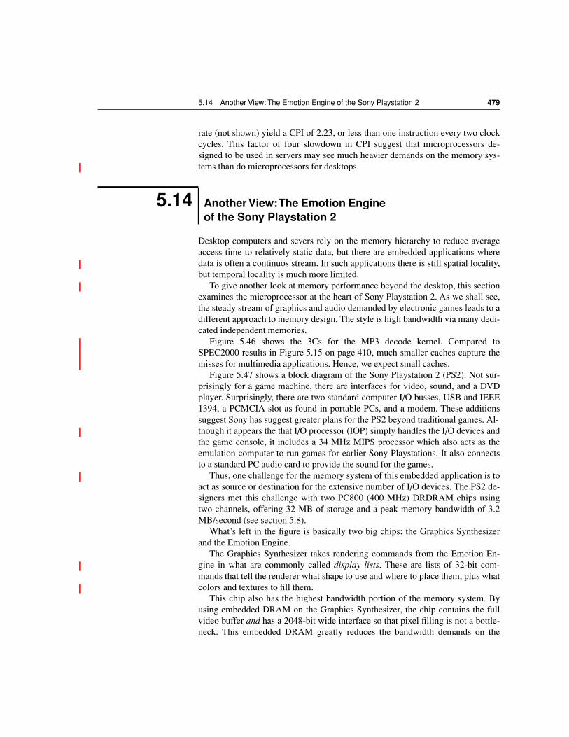
5.14 Another View: The Emotion Engine of the Sony Playstation 2 479
rate (not shown) yield a CPI of 2.23, or less than one instruction every two clockcycles. This factor of four slowdown in CPI suggest that microprocessors de-signed to be used in servers may see much heavier demands on the memory sys-tems than do microprocessors for desktops.
Desktop computers and severs rely on the memory hierarchy to reduce averageaccess time to relatively static data, but there are embedded applications wheredata is often a continuos stream. In such applications there is still spatial locality,but temporal locality is much more limited.
To give another look at memory performance beyond the desktop, this sectionexamines the microprocessor at the heart of Sony Playstation 2. As we shall see,the steady stream of graphics and audio demanded by electronic games leads to adifferent approach to memory design. The style is high bandwidth via many dedi-cated independent memories.
Figure 5.46 shows the 3Cs for the MP3 decode kernel. Compared toSPEC2000 results in Figure 5.15 on page 410, much smaller caches capture themisses for multimedia applications. Hence, we expect small caches.
Figure 5.47 shows a block diagram of the Sony Playstation 2 (PS2). Not sur-prisingly for a game machine, there are interfaces for video, sound, and a DVDplayer. Surprisingly, there are two standard computer I/O busses, USB and IEEE1394, a PCMCIA slot as found in portable PCs, and a modem. These additionssuggest Sony has suggest greater plans for the PS2 beyond traditional games. Al-though it appears the that I/O processor (IOP) simply handles the I/O devices andthe game console, it includes a 34 MHz MIPS processor which also acts as theemulation computer to run games for earlier Sony Playstations. It also connectsto a standard PC audio card to provide the sound for the games.
Thus, one challenge for the memory system of this embedded application is toact as source or destination for the extensive number of I/O devices. The PS2 de-signers met this challenge with two PC800 (400 MHz) DRDRAM chips usingtwo channels, offering 32 MB of storage and a peak memory bandwidth of 3.2MB/second (see section 5.8).
What’s left in the figure is basically two big chips: the Graphics Synthesizerand the Emotion Engine.
The Graphics Synthesizer takes rendering commands from the Emotion En-gine in what are commonly called display lists. These are lists of 32-bit com-mands that tell the renderer what shape to use and where to place them, plus whatcolors and textures to fill them.
This chip also has the highest bandwidth portion of the memory system. Byusing embedded DRAM on the Graphics Synthesizer, the chip contains the fullvideo buffer and has a 2048-bit wide interface so that pixel filling is not a bottle-neck. This embedded DRAM greatly reduces the bandwidth demands on the
5.14 Another View: The Emotion Engine of the Sony Playstation 2
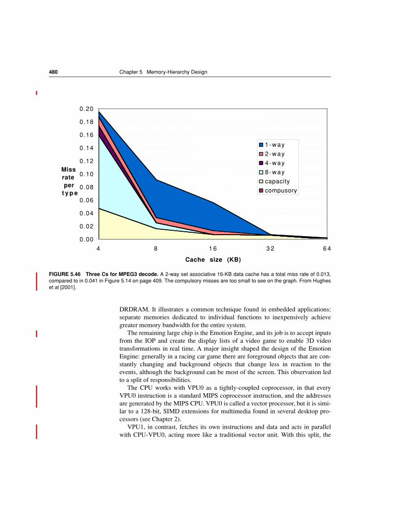
480 Chapter 5 Memory-Hierarchy Design
DRDRAM. It illustrates a common technique found in embedded applications:separate memories dedicated to individual functions to inexpensively achievegreater memory bandwidth for the entire system.
The remaining large chip is the Emotion Engine, and its job is to accept inputsfrom the IOP and create the display lists of a video game to enable 3D videotransformations in real time. A major insight shaped the design of the EmotionEngine: generally in a racing car game there are foreground objects that are con-stantly changing and background objects that change less in reaction to theevents, although the background can be most of the screen. This observation ledto a split of responsibilities.
The CPU works with VPU0 as a tightly-coupled coprocessor, in that everyVPU0 instruction is a standard MIPS coprocessor instruction, and the addressesare generated by the MIPS CPU. VPU0 is called a vector processor, but it is simi-lar to a 128-bit, SIMD extensions for multimedia found in several desktop pro-cessors (see Chapter 2).
VPU1, in contrast, fetches its own instructions and data and acts in parallelwith CPU-VPU0, acting more like a traditional vector unit. With this split, the
FIGURE 5.46 Three Cs for MPEG3 decode. A 2-way set associative 16-KB data cache has a total miss rate of 0.013,compared to in 0.041 in Figure 5.14 on page 409. The compulsory misses are too small to see on the graph. From Hugheset al [2001].
0.00
0.02
0.04
0.06
0.08
0.10
0.12
0.14
0.16
0.18
0.20
4 8 1 6 3 2 6 4
Cache size (KB)
Miss rate per
t y p e
1 -way
2 -way
4 -way
8 -way
capacity
compusory
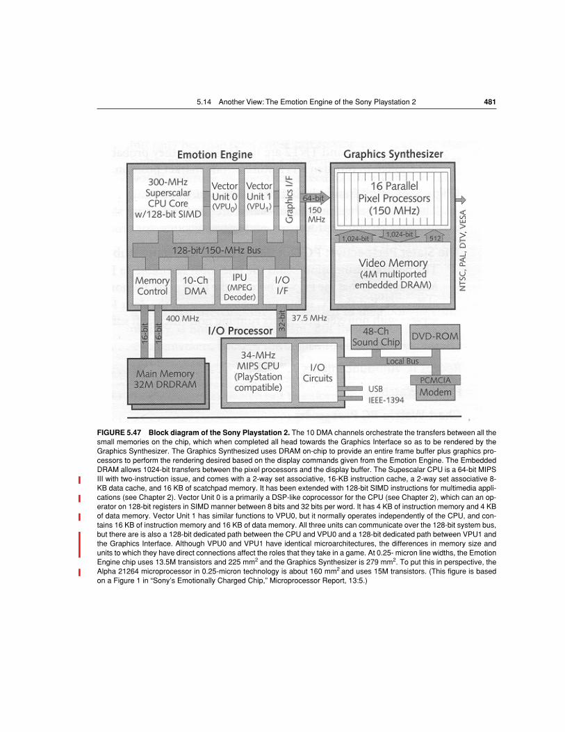
5.14 Another View: The Emotion Engine of the Sony Playstation 2 481
FIGURE 5.47 Block diagram of the Sony Playstation 2. The 10 DMA channels orchestrate the transfers between all thesmall memories on the chip, which when completed all head towards the Graphics Interface so as to be rendered by theGraphics Synthesizer. The Graphics Synthesized uses DRAM on-chip to provide an entire frame buffer plus graphics pro-cessors to perform the rendering desired based on the display commands given from the Emotion Engine. The EmbeddedDRAM allows 1024-bit transfers between the pixel processors and the display buffer. The Supescalar CPU is a 64-bit MIPSIII with two-instruction issue, and comes with a 2-way set associative, 16-KB instruction cache, a 2-way set associative 8-KB data cache, and 16 KB of scatchpad memory. It has been extended with 128-bit SIMD instructions for multimedia appli-cations (see Chapter 2). Vector Unit 0 is a primarily a DSP-like coprocessor for the CPU (see Chapter 2), which can an op-erator on 128-bit registers in SIMD manner between 8 bits and 32 bits per word. It has 4 KB of instruction memory and 4 KBof data memory. Vector Unit 1 has similar functions to VPU0, but it normally operates independently of the CPU, and con-tains 16 KB of instruction memory and 16 KB of data memory. All three units can communicate over the 128-bit system bus,but there are is also a 128-bit dedicated path between the CPU and VPU0 and a 128-bit dedicated path between VPU1 andthe Graphics Interface. Although VPU0 and VPU1 have identical microarchitectures, the differences in memory size andunits to which they have direct connections affect the roles that they take in a game. At 0.25- micron line widths, the EmotionEngine chip uses 13.5M transistors and 225 mm2 and the Graphics Synthesizer is 279 mm2. To put this in perspective, theAlpha 21264 microprocessor in 0.25-micron technology is about 160 mm2 and uses 15M transistors. (This figure is basedon a Figure 1 in “Sony’s Emotionally Charged Chip,” Microprocessor Report, 13:5.)
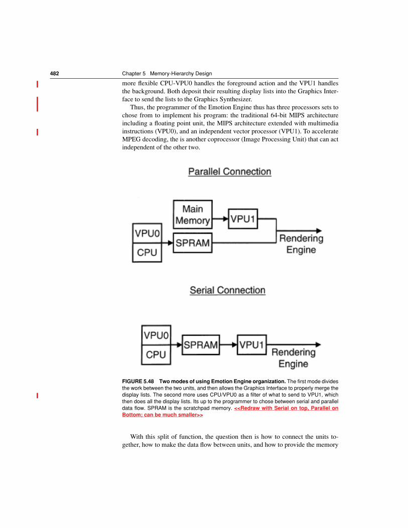
482 Chapter 5 Memory-Hierarchy Design
more flexible CPU-VPU0 handles the foreground action and the VPU1 handlesthe background. Both deposit their resulting display lists into the Graphics Inter-face to send the lists to the Graphics Synthesizer.
Thus, the programmer of the Emotion Engine thus has three processors sets tochose from to implement his program: the traditional 64-bit MIPS architectureincluding a floating point unit, the MIPS architecture extended with multimediainstructions (VPU0), and an independent vector processor (VPU1). To accelerateMPEG decoding, the is another coprocessor (Image Processing Unit) that can actindependent of the other two.
With this split of function, the question then is how to connect the units to-gether, how to make the data flow between units, and how to provide the memory
FIGURE 5.48 Two modes of using Emotion Engine organization. The first mode dividesthe work between the two units, and then allows the Graphics Interface to properly merge thedisplay lists. The second more uses CPU/VPU0 as a filter of what to send to VPU1, whichthen does all the display lists. Its up to the programmer to chose between serial and paralleldata flow. SPRAM is the scratchpad memory. <<Redraw with Serial on top, Parallel onBottom; can be much smaller>>
5.15 Another View: The Sun Fire 6800 Server 483
bandwidth needed by all these units. As mentioned above, the Emotion Enginedesigners chose many dedicated memories. The CPU has a 16-KB scatchpadmemory (SPRAM) in addition to a 16-KB instruction cache and an 8-KB datacache. VPU0 has a 4-KB instruction memory and a 4-KB data memory, andVPU1 has a 16-KB instruction memory and a 16-KB data memory. Note thatthese are four memories, not caches of a larger memory elsewhere. In each mem-ory the latency is just one clock cycle. VPU1 has more memory than VPU0 be-cause it creates the bulk of the display lists and because it largely actsindependently.
The programmer organizes all memories as two double buffers, one pair forthe incoming DMA data and one pair for the outgoing DMA data. The program-mer then uses the various processors to transform the data from the input bufferto the output buffer. To keep the data flowing among the units, the programmernext sets up the 10 DMA channels, taking care to meet the real time deadline forrealistic animation of 15 frame per second.
Figure 5.48 shows that this organization supports two main operating modes:serial where CPU/VPU0 act as a preprocessor on what to give VPU1 for it to cre-ate for the Graphics Interface using the scratchpad memory as the buffer, and par-allel where both the CPU/VPU0 and VPU1 create display lists. The display listsand the Graphics Synthesizer have multiple context identifiers to distinguish theparallel display lists to produce a coherent final image.
All units in the Emotion Engine are linked by a common 150 Mhz, 128-bitwide bus. To offer greater bandwidth, there are also two dedicated buses: a 128-bit path between the CPU and VPU0, and a 128-bit path between VPU1 and theGraphics Interface. The programmer also chooses which bus to use when settingup the DMA channels.
Taking the big picture, if a server-oriented designer had been given the prob-lem we might see a single common bus with many local caches and cache coher-ent mechanism to keep data consistent. In contrast, the Playstation 2 followed thetradition of embedded designers and has at least nine distinct memory modules.To keep the data flowing in real time from memory to the display the PS2 usesdedicated memories, dedicated buses, and DMA channels. Coherency is the re-sponsibility of the programmer, and given the continuous flow from main memo-ry to the graphics interface and the real time requirements, programmercontrolled coherency works well for this application.
The Sun Fire 6800 is a mid range multiprocessor server with particular attentionpaid to the memory system. The emphasis of this server is cost-performance forboth commercial computing, running data base applications such data warehous-ing and data mining, as well as high performance computing. This server also in-cludes special features to improve availability and maintainability.
5.15 Another View: The Sun Fire 6800 Server
484 Chapter 5 Memory-Hierarchy Design
Given these goals, what should be the size of the caches? Looking at theSPEC2000 results in Figure 5.17 on page 413 suggests miss rates of 0.5% for a1-MB data cache, with infinitesimal instruction cache miss rates at those sizes. Itwould seem that a 1-MB off chip cache should be sufficient.
Commercial workloads, however, get very different results. Figure 5.49 showsthe impact on the off chip cache for an Alpha 21164 server running commercialworkloads. Unlike the results for SPEC2000, commercial workloads running da-tabase applications have significant misses just for instructions with a 1-mega-byte cache. The reason is that code size of commercial databases is measured inmillions of lines of code, unlike any SPEC2000 benchmark. Second, note that ca-pacity and conflict misses remain significant until cache size becomes 4 to 8megabyte. Note that even compulsory misses lead to a measurable causes higherCPI; this is because servers often run many processes, which results in many con-text switches and thus more compulsory misses. Finally, there is a new categoryof misses in a multiprocessor, and these are due to having to keep all the cachesof a multiprocessor coherent, a problem mentioned in section 5.12. These aresometimes called coherency misses, adding a fourth C to our three C model fromsection 5.5. Chapter 6 explains a good deal more about coherence or sharing traf-fic in multiprocessors. The data suggests that commercial workloads need con-siderably bigger off-chip caches than do SPEC2000.
Figure 5.50 shows the essential characteristics of the Sun Fire 6800 that thedesigners selected. Note the 8 MB L2 cache, which is in response to the commer-cial needs.
The microprocessor that drives this server is the UltraSPARC III. One strikingfeature of the chip is the number of pins: 1368 in a Ball Grid Array. Figure 5.51shows how one chip could use so many pins. The L2 caches bus operates at 200MHz, local memory at 75 MHz, and the rest operate at 150 MHz. The combina-tion of UltraSPARC III and the data switch yields a peak bandwidth to off chipmemory of 11 Gbytes/second.
Note that the several wide buses include error correction bits in Figure 5.51.Error correction codes enable buses and memories to both detect and correct er-rors. The idea is to calculate and storage parity over different subsets of the bitsin the protected word. When parity does not match it indicates an error. By look-ing at which of the overlapping subsets have a parity error and which don’t, itspossible to determine the bit that failed. The Sun Fire ECC was also designed todetect any pair of bit errors, and also to detect if a whole DRAM chip failed turn-ing all the bits of an 8-bit wide chip to zero. Such codes are generally classifiedas Single Error Correcting/Double Error Detecting (SEC/DED). The UltraS-PARC sends these ECC bits between the memory chips and the microprocessor,so that errors that occur on the high-speed buses are also detected and corrected.
In addition to several wide busses for memory bandwidth, the designers of Ul-traSPARC were concerned about latency. Hence, the chip includes a DRAM con-troller on the chip, which they claim saved 80 ns of latency. The result is 220 nsto the local memory and 280 ns to the non-local memory. (This server supportsnon-uniform memory access shared memory, described in Chapter 6.) Since
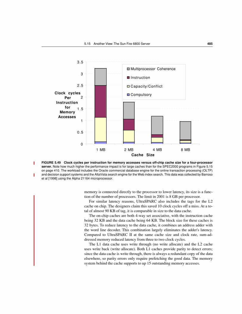
5.15 Another View: The Sun Fire 6800 Server 485
memory is connected directly to the processor to lower latency, its size is a func-tion of the number of processors. The limit in 2001 is 8 GB per processor.
For similar latency reasons, UltraSPARC also includes the tags for the L2cache on chip. The designers claim this saved 10 clock cycles off a miss. At a to-tal of almost 90 KB of tag, it is comparable in size to the data cache.
The on-chip caches are both 4-way set associative, with the instruction cachebeing 32 KB and the data cache being 64 KB. The block size for these caches is32 bytes. To reduce latency to the data cache, it combines an address adder withthe word line decoder. This combination largely eliminates the adder's latency.Compared to UltraSPARC II at the same cache size and clock rate, sum-ad-dressed memory reduced latency from three to two clock cycles.
The L1 data cache uses write through (no write allocate) and the L2 cacheuses write back (write allocate). Both L1 caches provide parity to detect errors;since the data cache is write through, there is always a redundant copy of the dataelsewhere, so parity errors only require prefetching the good data. The memorysystem behind the cache supports to up 15 outstanding memory accesses.
FIGURE 5.49 Clock cycles per instruction for memory accesses versus off-chip cache size for a four-processorserver. Note how much higher the performance impact is for large caches than for the SPEC2000 programs in Figure 5.15on page 410. The workload includes the Oracle commercial database engine for the online transaction processing (OLTP)and decision support systems and the AltaVista search engine for the Web index search. This data was collected by Barrosoet al [1998] using the Alpha 21164 microprocessor.
0
0.5
1
1.5
2
2.5
3
3.5
1 MB 2 MB 4 MB 8 MBCache Size
Clock cycles Per
Instruction for
Memory Accesses
Multiprocessor Coherence
Instruction
Capacity/Conflict
Compulsory
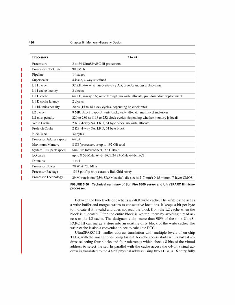
486 Chapter 5 Memory-Hierarchy Design
Between the two levels of cache is a 2-KB write cache. The write cache act asa write buffer and merges writes to consecutive locations. It keeps a bit per byteto indicate if it is valid and does not read the block from the L2 cache when theblock is allocated. Often the entire block is written, there by avoiding a read ac-cess to the L2 cache. The designers claim more than 90% of the time UltraS-PARC III can merge a store into an existing dirty block of the write cache. Thewrite cache is also a convenient place to calculate ECC.
UltraSPARC III handles address translation with multiple levels of on-chipTLBs, with the smaller ones being fastest. A cache access starts with a virtual ad-dress selecting four blocks and four microtags which checks 8 bits of the virtualaddress to select the set. In parallel with the cache access the 64-bit virtual ad-dress is translated to the 43-bit physical address using two TLBs: a 16 entry fully
Processors 2 to 24
Processors 2 to 24 UltraSPARC III processors
Processor Clock rate 900 MHz
Pipeline 14 stages
Superscalar 4-issue, 4-way sustained
L1 I cache 32 KB, 4-way set associative (S.A.), pseudorandom replacement
L1 I cache latency 2 clocks
L1 D cache 64 KB, 4-way SA; write through, no write allocate, pseudorandom replacement
L1 D cache latency 2 clocks
L1 I/D miss penalty 20 ns (15 to 18 clock cycles, depending on clock rate)
L2 cache 8 MB, direct mapped; write back, write allocate, multilevel inclusion
L2 miss penalty 220 to 280 ns (198 to 252 clock cycles, depending whether memory is local)
Write Cache 2 KB, 4-way SA, LRU, 64 byte block, no write allocate
Prefetch Cache 2 KB, 4-way SA, LRU, 64 byte block
Block size 32 bytes
Processor Address space 64 bit
Maximum Memory 8 GB/processor, or up to 192 GB total
System Bus, peak speed Sun Fire Interconnect, 9.6 GB/sec
I/O cards up to 8 66-MHz, 64-bit PCI, 24 33-MHz 64-bit PCI
Domains 1 to 4
Processor Power 70 W at 750 MHz
Processor Package 1368 pin flip-chip ceramic Ball Grid Array
Processor Technology 29 M transistors (75% SRAM cache), die size is 217 mm2; 0.15 micron, 7-layer CMOS
FIGURE 5.50 Technical summary of Sun Fire 6800 server and UltraSPARC III micro-processor.
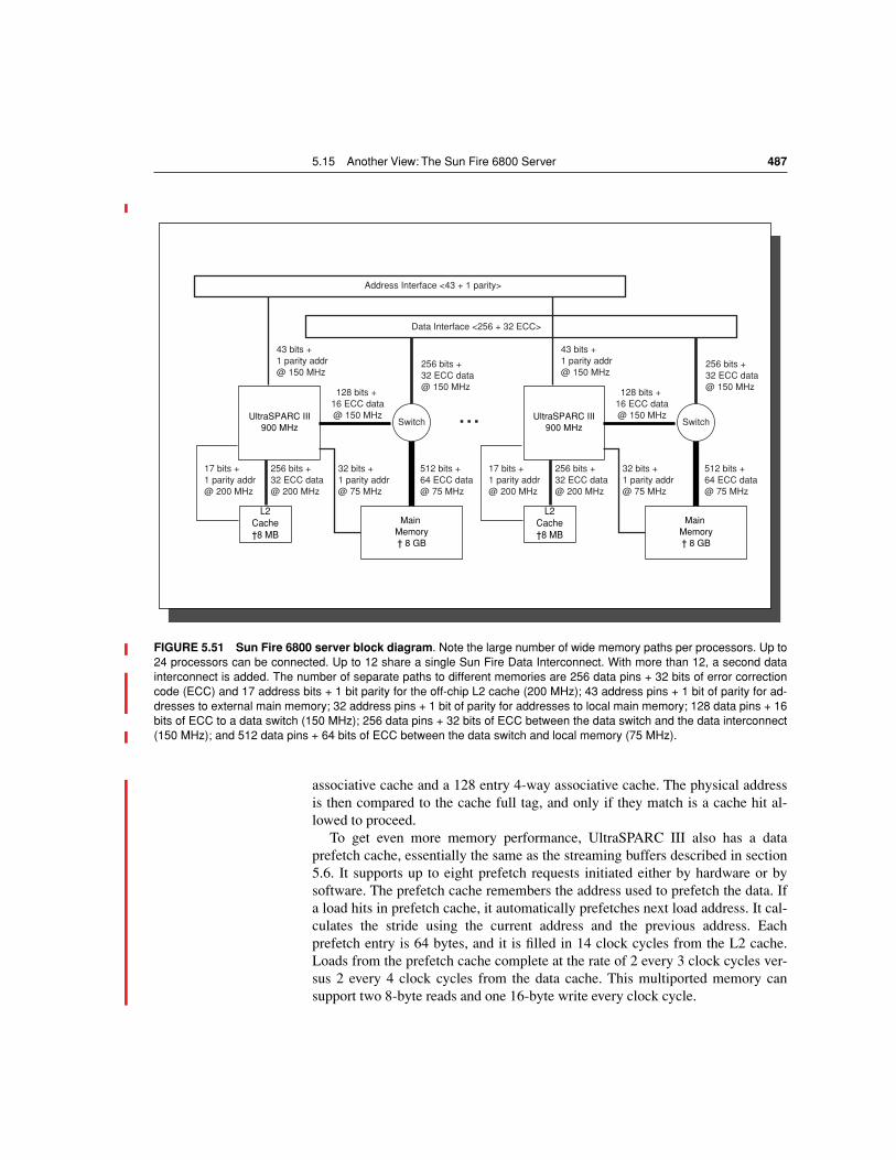
5.15 Another View: The Sun Fire 6800 Server 487
associative cache and a 128 entry 4-way associative cache. The physical addressis then compared to the cache full tag, and only if they match is a cache hit al-lowed to proceed.
To get even more memory performance, UltraSPARC III also has a dataprefetch cache, essentially the same as the streaming buffers described in section5.6. It supports up to eight prefetch requests initiated either by hardware or bysoftware. The prefetch cache remembers the address used to prefetch the data. Ifa load hits in prefetch cache, it automatically prefetches next load address. It cal-culates the stride using the current address and the previous address. Eachprefetch entry is 64 bytes, and it is filled in 14 clock cycles from the L2 cache.Loads from the prefetch cache complete at the rate of 2 every 3 clock cycles ver-sus 2 every 4 clock cycles from the data cache. This multiported memory cansupport two 8-byte reads and one 16-byte write every clock cycle.
FIGURE 5.51 Sun Fire 6800 server block diagram. Note the large number of wide memory paths per processors. Up to24 processors can be connected. Up to 12 share a single Sun Fire Data Interconnect. With more than 12, a second datainterconnect is added. The number of separate paths to different memories are 256 data pins + 32 bits of error correctioncode (ECC) and 17 address bits + 1 bit parity for the off-chip L2 cache (200 MHz); 43 address pins + 1 bit of parity for ad-dresses to external main memory; 32 address pins + 1 bit of parity for addresses to local main memory; 128 data pins + 16bits of ECC to a data switch (150 MHz); 256 data pins + 32 bits of ECC between the data switch and the data interconnect(150 MHz); and 512 data pins + 64 bits of ECC between the data switch and local memory (75 MHz).
Address Interface <43 + 1 parity>
Data Interface <256 + 32 ECC>
...
L2Cache†8 MB
UltraSPARC III900 MHz
256 bits + 32 ECC data@ 200 MHz
512 bits + 64 ECC data@ 75 MHz
128 bits + 16 ECC data@ 150 MHz
256 bits + 32 ECC data@ 150 MHz
32 bits + 1 parity addr@ 75 MHz
43 bits + 1 parity addr@ 150 MHz
17 bits + 1 parity addr@ 200 MHz
Switch
Main Memory† 8 GB
L2Cache†8 MB
UltraSPARC III900 MHz
256 bits + 32 ECC data@ 200 MHz
512 bits + 64 ECC data@ 75 MHz
128 bits + 16 ECC data@ 150 MHz
256 bits + 32 ECC data@ 150 MHz
32 bits + 1 parity addr@ 75 MHz
43 bits + 1 parity addr@ 150 MHz
17 bits + 1 parity addr@ 200 MHz
Switch
Main Memory† 8 GB
488 Chapter 5 Memory-Hierarchy Design
In addition to prefetching data, UltraSPARC III has a small instructionprefetch buffer of 32 bytes that tries to stay one block ahead of the instruction de-coder. On an instruction cache miss, two blocks are requested: one for the in-struction cache and one for the instruction prefetch buffer. The buffer is then usedto fill the cache if a sequential access also misses. In addition to parity and ECCto help with dependability, Sun Fire 6800 server offers up to four dynamic systemdomains. This option allows the computer to be divided into quarters or halves,with each piece running its own version of the operating system independently.Thus, a hardware or software failure in one piece does not affect applications run-ning on the rest of the computer. The dynamic portion of the name means the re-configuration can occur without rebooting the system.
To help diagnose problems, every UltraSPARC III has an 8-bit ``back door''bus that runs independently from the main buses. If the system bus has an error,processors can still boot and run diagnostic programs over this back door bus todiagnose the problem.
Among the other availability features of the 6800 is a redundant path betweenthe processors. Each system has two networks to connect the 24 processors to-gether so that if one fails the system still works. Similarly, each Sun Fire inter-connect has two crossbar chips to link it to the processor board, so that onecrossbar chip can fail and yet the board can still communicate. There are alsodual redundant system controllers that monitors server operation, and so they areable to notify administrators when problems are detected. Administrators can usethe controllers to remotely initiate diagnostics and corrective actions.
In summary, the Sun Fire 6800 server and its processor pay much greater at-tention to dependability, memory latency and bandwidth, and system scalabilitythan do desktop computers and processors.
As the most naturally quantitative of the computer architecture disciplines, mem-ory hierarchy would seem to be less vulnerable to fallacies and pitfalls. Yet theauthors were limited here not by lack of warnings, but by lack of space!
Fallacy: Predicting cache performance of one program from another.
Figure 5.14 on page 409 shows the instruction miss rates and data miss rates forthree programs from the SPEC2000 benchmark suite as cache size varies. De-pending on the program, the data misses per thousand instructions for a 4096-KBcache is 9, 2, or 90, and the instruction misses per thousand instructions for a 4-KB cache is 55, 19, or 0.0004. Figure 5.45 on page 478 shows that commercialprograms such as databases will have significant miss rates even in a 8-MB sec-ond-level cache, which is generally not the case for the SPEC programs. Similar-ly, MPEG3 decode in Figure 5.46 on page 480 fits entirely in a 64 KB data cache,
5.16 Fallacies and Pitfalls
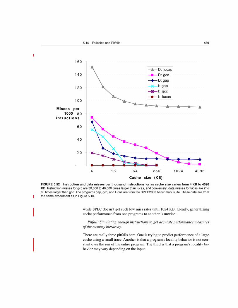
5.16 Fallacies and Pitfalls 489
while SPEC doesn’t get such low miss rates until 1024 KB. Clearly, generalizingcache performance from one programs to another is unwise.
Pitfall: Simulating enough instructions to get accurate performance measuresof the memory hierarchy.
There are really three pitfalls here. One is trying to predict performance of a largecache using a small trace. Another is that a program's locality behavior is not con-stant over the run of the entire program. The third is that a program's locality be-havior may vary depending on the input.
FIGURE 5.52 Instruction and data misses per thousand instructions for as cache size varies from 4 KB to 4096KB. Instruction misses for gcc are 30,000 to 40,000 times larger than lucas, and conversely, data misses for lucas are 2 to60 times larger than gcc. The programs gap, gcc, and lucas are from the SPEC2000 benchmark suite. These data are fromthe same experiment as in Figure 5.10.
-
2 0
4 0
6 0
8 0
100
120
140
160
4 1 6 6 4 256 1024 4096
Cache size (KB)
Misses per 1000
in t ruct ions
D: lucas
D: gcc
D: gap
I: gap
I: gcc
I: lucas
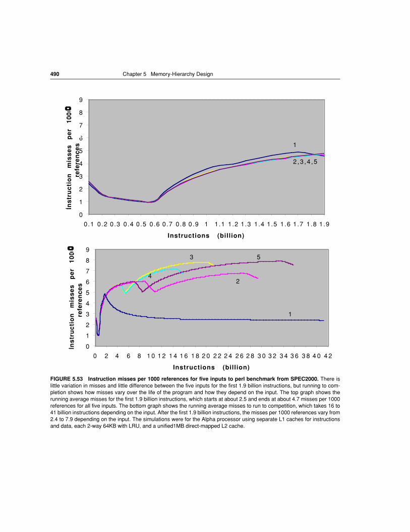
490 Chapter 5 Memory-Hierarchy Design
FIGURE 5.53 Instruction misses per 1000 references for five inputs to perl benchmark from SPEC2000. There islittle variation in misses and little difference between the five inputs for the first 1.9 billion instructions, but running to com-pletion shows how misses vary over the life of the program and how they depend on the input. The top graph shows therunning average misses for the first 1.9 billion instructions, which starts at about 2.5 and ends at about 4.7 misses per 1000references for all five inputs. The bottom graph shows the running average misses to run to competition, which takes 16 to41 billion instructions depending on the input. After the first 1.9 billion instructions, the misses per 1000 references vary from2.4 to 7.9 depending on the input. The simulations were for the Alpha processor using separate L1 caches for instructionsand data, each 2-way 64KB with LRU, and a unified1MB direct-mapped L2 cache.
0
1
2
3
4
5
6
7
8
9
0 2 4 6 8 1 0 1 2 1 4 1 6 1 8 2 0 2 2 2 4 2 6 2 8 3 0 3 2 3 4 3 6 3 8 4 0 4 2
Instructions (billion)
Ins
tru
cti
on
m
iss
es
p
er
10
00
re
fere
nce
s
1
2
3
4
5
0
1
2
3
4
5
6
7
8
9
0.1 0.2 0.3 0.4 0.5 0.6 0.7 0.8 0.9 1 1.1 1.2 1.3 1.4 1.5 1.6 1.7 1.8 1.9
Instructions (billion)
Ins
tru
cti
on
m
iss
es
p
er
10
00
re
fere
nce
s
1
2 ,3 ,4 ,5
5.16 Fallacies and Pitfalls 491
Figure 5.53 shows the cumulative average instruction misses per thousand in-structions for five inputs to a single SPEC2000 program. For these inputs, the av-erage memory rate for the first 1.9 billion instructions is very different from theiraverage miss rate for the rest of the execution.
The first edition of this book included another example of this pitfall. Thecompulsory miss ratios were erroneously high (e.g., 1%) because of tracing toofew memory accesses. A program with an compulsory cache miss ratio of 1%running on a computer accessing memory 10 million times per second (at thetime of the first edition) would access hundreds of megabytes of memory per sec-ond:
Data on typical page fault rates and process sizes do not support the conclusionthat memory is touched at this rate.
Pitfall: Too small an address space.
Just five years after DEC and Carnegie Mellon University collaborated to designthe new PDP-11 computer family, it was apparent that their creation had a fatalflaw. An architecture announced by IBM six years before the PDP-11 was stillthriving, with minor modifications, 25 years later. And the DEC VAX, criticizedfor including unnecessary functions, sold millions of units after the PDP-11 wentout of production. Why?
The fatal flaw of the PDP-11 was the size of its addresses (16 bits) as com-pared to the address sizes of the IBM 360 (24 to 31 bits) and the VAX (32 bits).Address size limits the program length, since the size of a program and theamount of data needed by the program must be less than 2address size. The reasonthe address size is so hard to change is that it determines the minimum width ofanything that can contain an address: PC, register, memory word, and effective-address arithmetic. If there is no plan to expand the address from the start, thenthe chances of successfully changing address size are so slim that it normallymeans the end of that computer family. Bell and Strecker [1976] put it like this:
There is only one mistake that can be made in computer design that is difficult torecover from—not having enough address bits for memory addressing and mem-ory management. The PDP-11 followed the unbroken tradition of nearly everyknown computer. [p. 2]
A partial list of successful computers that eventually starved to death for lack ofaddress bits includes the PDP-8, PDP-10, PDP-11, Intel 8080, Intel 8086, Intel80186, Intel 80286, Motorola AMI 6502, Zilog Z80, CRAY-1, and CRAY X-MP.
10,000,000 accessesSecond------------------------------------------------
0.01 missesAccess----------------------------× 32 bytes
Miss--------------------× 60 secondsMinute--------------------------
192,000,000 bytesMinute--------------------------------------------
=×
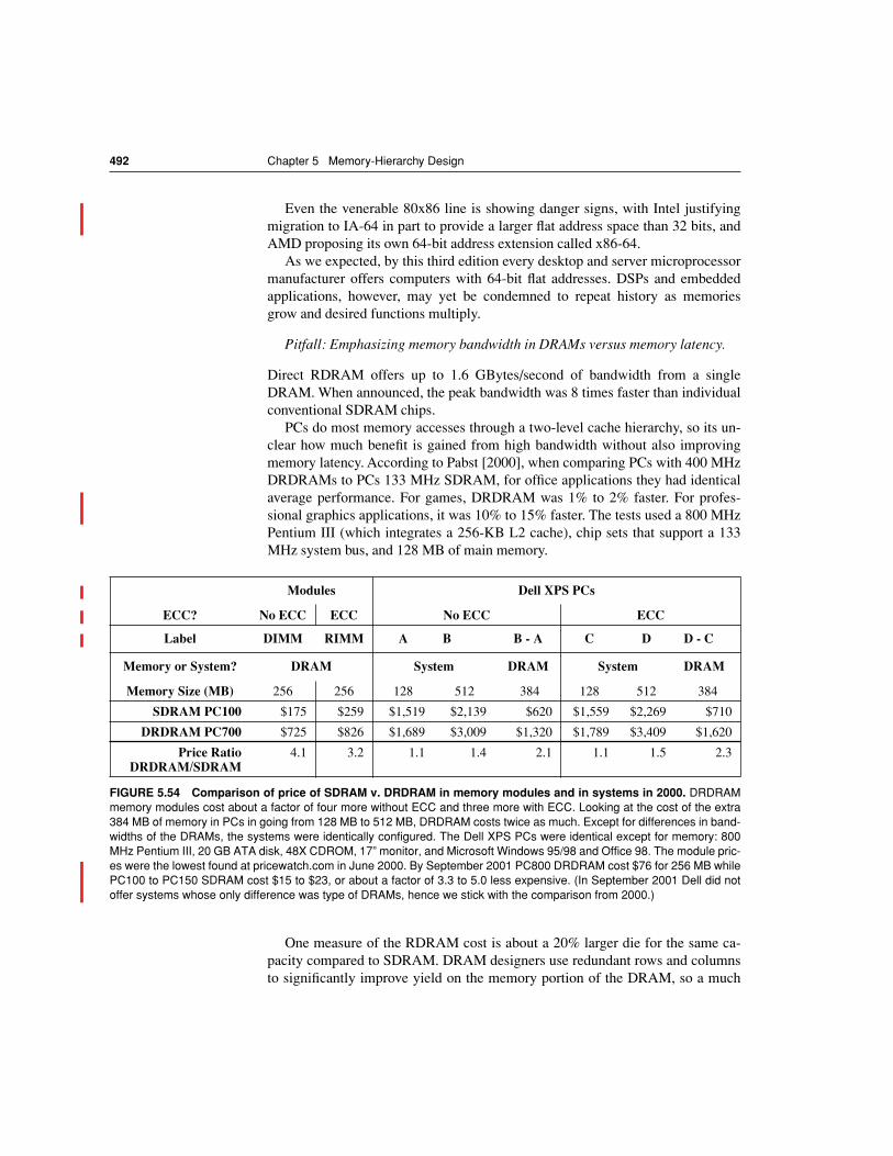
492 Chapter 5 Memory-Hierarchy Design
Even the venerable 80x86 line is showing danger signs, with Intel justifyingmigration to IA-64 in part to provide a larger flat address space than 32 bits, andAMD proposing its own 64-bit address extension called x86-64.
As we expected, by this third edition every desktop and server microprocessormanufacturer offers computers with 64-bit flat addresses. DSPs and embeddedapplications, however, may yet be condemned to repeat history as memoriesgrow and desired functions multiply.
Pitfall: Emphasizing memory bandwidth in DRAMs versus memory latency.
Direct RDRAM offers up to 1.6 GBytes/second of bandwidth from a singleDRAM. When announced, the peak bandwidth was 8 times faster than individualconventional SDRAM chips.
PCs do most memory accesses through a two-level cache hierarchy, so its un-clear how much benefit is gained from high bandwidth without also improvingmemory latency. According to Pabst [2000], when comparing PCs with 400 MHzDRDRAMs to PCs 133 MHz SDRAM, for office applications they had identicalaverage performance. For games, DRDRAM was 1% to 2% faster. For profes-sional graphics applications, it was 10% to 15% faster. The tests used a 800 MHzPentium III (which integrates a 256-KB L2 cache), chip sets that support a 133MHz system bus, and 128 MB of main memory.
One measure of the RDRAM cost is about a 20% larger die for the same ca-pacity compared to SDRAM. DRAM designers use redundant rows and columnsto significantly improve yield on the memory portion of the DRAM, so a much
Modules Dell XPS PCs
ECC? No ECC ECC No ECC ECC
Label DIMM RIMM A B B - A C D D - C
Memory or System? DRAM System DRAM System DRAM
Memory Size (MB) 256 256 128 512 384 128 512 384
SDRAM PC100 $175 $259 $1,519 $2,139 $620 $1,559 $2,269 $710
DRDRAM PC700 $725 $826 $1,689 $3,009 $1,320 $1,789 $3,409 $1,620
Price RatioDRDRAM/SDRAM
4.1 3.2 1.1 1.4 2.1 1.1 1.5 2.3
FIGURE 5.54 Comparison of price of SDRAM v. DRDRAM in memory modules and in systems in 2000. DRDRAMmemory modules cost about a factor of four more without ECC and three more with ECC. Looking at the cost of the extra384 MB of memory in PCs in going from 128 MB to 512 MB, DRDRAM costs twice as much. Except for differences in band-widths of the DRAMs, the systems were identically configured. The Dell XPS PCs were identical except for memory: 800MHz Pentium III, 20 GB ATA disk, 48X CDROM, 17” monitor, and Microsoft Windows 95/98 and Office 98. The module pric-es were the lowest found at pricewatch.com in June 2000. By September 2001 PC800 DRDRAM cost $76 for 256 MB whilePC100 to PC150 SDRAM cost $15 to $23, or about a factor of 3.3 to 5.0 less expensive. (In September 2001 Dell did notoffer systems whose only difference was type of DRAMs, hence we stick with the comparison from 2000.)
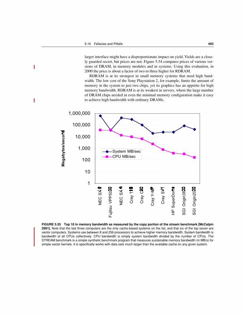
5.16 Fallacies and Pitfalls 493
larger interface might have a disproportionate impact on yield. Yields are a close-ly guarded secret, but prices are not. Figure 5.54 compares prices of various ver-sions of DRAM, in memory modules and in systems. Using this evaluation, in2000 the price is about a factor of two to three higher for RDRAM.
RDRAM is at its strongest in small memory systems that need high band-width. The low cost of the Sony Playstation 2, for example, limits the amount ofmemory in the system to just two chips, yet its graphics has an appetite for highmemory bandwidth. RDRAM is at its weakest in servers, where the large numberof DRAM chips needed in even the minimal memory configuration make it easyto achieve high bandwidth with ordinary DRAMs.
FIGURE 5.55 Top 10 in memory bandwidth as measured by the copy portion of the stream benchmark [McCalpin2001]. Note that the last three computers are the only cache-based systems on the list, and that six of the top seven arevector computers. Systems use between 8 and 256 processors to achieve higher memory bandwidth. System bandwidth isbandwidth of all CPUs collectively. CPU bandwidth is simply system bandwidth divided by the number of CPUs. TheSTREAM benchmark is a simple synthetic benchmark program that measures sustainable memory bandwidth (in MB/s) forsimple vector kernels. It is specifically works with data sets much larger than the available cache on any given system.
1
10
100
1,000
10,000
100,000
1,000,000
NE
C S
X 5
Fuj
itsu
VP
P50
00
NE
C S
X 4
Cra
y T
3E
Cra
y C
90
Cra
y Y
-MP
Cra
y S
V1
HP
Sup
erD
ome
SG
I O
rigin
3800
SG
I O
rigin
2000
Meg
abyt
es/s
eco
nd
System MB/secCPU MB/sec
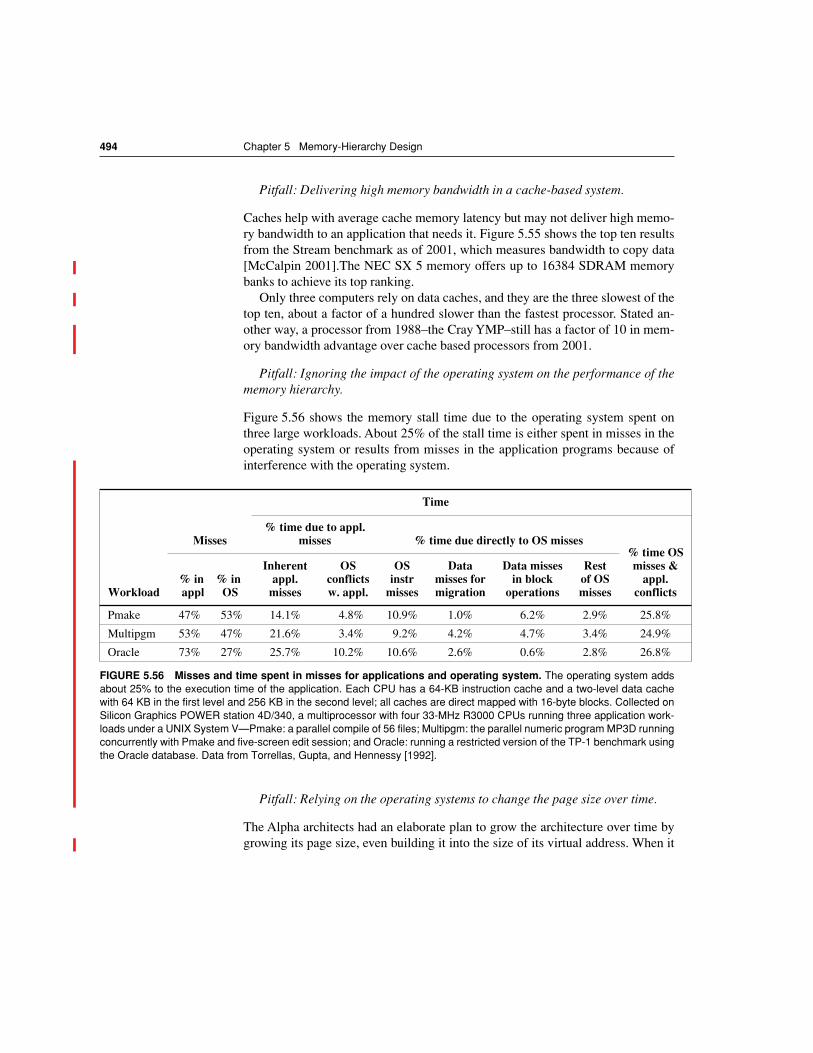
494 Chapter 5 Memory-Hierarchy Design
Pitfall: Delivering high memory bandwidth in a cache-based system.
Caches help with average cache memory latency but may not deliver high memo-ry bandwidth to an application that needs it. Figure 5.55 shows the top ten resultsfrom the Stream benchmark as of 2001, which measures bandwidth to copy data[McCalpin 2001].The NEC SX 5 memory offers up to 16384 SDRAM memorybanks to achieve its top ranking.
Only three computers rely on data caches, and they are the three slowest of thetop ten, about a factor of a hundred slower than the fastest processor. Stated an-other way, a processor from 1988–the Cray YMP–still has a factor of 10 in mem-ory bandwidth advantage over cache based processors from 2001.
Pitfall: Ignoring the impact of the operating system on the performance of thememory hierarchy.
Figure 5.56 shows the memory stall time due to the operating system spent onthree large workloads. About 25% of the stall time is either spent in misses in theoperating system or results from misses in the application programs because ofinterference with the operating system.
Pitfall: Relying on the operating systems to change the page size over time.
The Alpha architects had an elaborate plan to grow the architecture over time bygrowing its page size, even building it into the size of its virtual address. When it
Time
Misses% time due to appl.
misses % time due directly to OS misses% time OSmisses &
appl.conflictsWorkload
% in % inappl OS
Inherentappl.
misses
OSconflictsw. appl.
OSinstr
misses
Datamisses formigration
Data missesin block
operations
Rest of OSmisses
Pmake 47% 53% 14.1% 4.8% 10.9% 1.0% 6.2% 2.9% 25.8%
Multipgm 53% 47% 21.6% 3.4% 9.2% 4.2% 4.7% 3.4% 24.9%
Oracle 73% 27% 25.7% 10.2% 10.6% 2.6% 0.6% 2.8% 26.8%
FIGURE 5.56 Misses and time spent in misses for applications and operating system. The operating system addsabout 25% to the execution time of the application. Each CPU has a 64-KB instruction cache and a two-level data cachewith 64 KB in the first level and 256 KB in the second level; all caches are direct mapped with 16-byte blocks. Collected onSilicon Graphics POWER station 4D/340, a multiprocessor with four 33-MHz R3000 CPUs running three application work-loads under a UNIX System V—Pmake: a parallel compile of 56 files; Multipgm: the parallel numeric program MP3D runningconcurrently with Pmake and five-screen edit session; and Oracle: running a restricted version of the TP-1 benchmark usingthe Oracle database. Data from Torrellas, Gupta, and Hennessy [1992].
5.17 Concluding Remarks 495
became time to grow page sizes with later Alphas, the operating system designersbalked and the virtual memory system was revised to grow the address spacewhile maintaining the 8-KB page.
Architects of other computers noticed very high TLB miss rates, and so addedmultiple, larger page sizes to the TLB. The hope was that operating systems pro-grammers would allocate an object to the largest page that made sense, therebypreserving TLB entries. After a decade of trying, most operating systems usethese “superpages” only for handpicked functions: mapping the display memoryor other I/O devices, or using very large pages for the database code.
Figure 5.57 compares the memory hierarchy of microprocessors aimed at desk-top, server, and embedded applications. The L1 caches are similar across applica-tions, with the primary differences being L2 cache size, die size, processor clockrate, and instructions issued per clock.
In contrast to showing the state of the art in a given year, Figure 5.56 showsevolution over a decade of the memory hierarchy of Alpha microprocessors andsystems. The primary change between the Alpha 21064 and 21364 is the hun-dredfold increase in on-chip cache size, which tries to compensate for the sixfoldincrease in main memory latency as measured in instructions.
The difficulty of building a memory system to keep pace with faster CPUs isunderscored by the fact that the raw material for main memory is the same as thatfound in the cheapest computer. It is the principle of locality that saves us here—its soundness is demonstrated at all levels of the memory hierarchy in currentcomputers, from disks to TLBs. One question is whether increasing scale breaksany of our assumptions. Are L3 caches bigger than prior main memories a cost-effective solution? Do 8 KB pages makes sense with terabyte main memories?
The design decisions at all these levels interact, and the architect must take thewhole system view to make wise decisions. The primary challenge for thememory-hierarchy designer is in choosing parameters that work well together,not in inventing new techniques. The increasingly fast CPUs are spending alarger fraction of time waiting for memory, which has led to new inventions thathave increased the number of choices: prefetching, cache-aware compilers, andincreasing page size. Fortunately, there tends to be a technological “sweet spot”in balancing cost, performance, power, and complexity: missing the target wastesperformance, power, hardware, design time, debug time, or possibly all five. Ar-chitects hit the target by careful, quantitative analysis.
5.17 Concluding Remarks
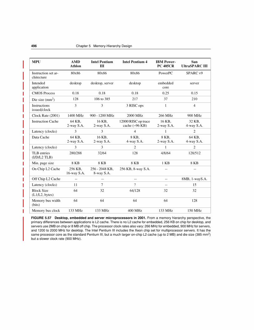
496 Chapter 5 Memory-Hierarchy Design
MPU AMD Athlon
Intel Pentium III
Intel Pentium 4 IBM Power-PC 405CR
Sun UltraSPARC III
Instruction set ar-chitecture
80x86 80x86 80x86 PowerPC SPARC v9
Intended application
desktop desktop, server desktop embedded core
server
CMOS Process 0.18 0.18 0.18 0.25 0.15
Die size (mm2) 128 106 to 385 217 37 210
Instructions issued/clock
3 3 3 RISC ops 1 4
Clock Rate (2001) 1400 MHz 900 - 1200 MHz 2000 MHz 266 MHz 900 MHz
Instruction Cache 64 KB, 2-way S.A.
16 KB, 2-way S.A.
12000 RISC op trace cache (~96 KB)
16 KB, 2-way S.A.
32 KB, 4-way S.A.
Latency (clocks) 3 3 4 1 2
Data Cache 64 KB, 2-way S.A.
16 KB, 2-way S.A.
8 KB, 4-way S.A.
8 KB, 2-way S.A.
64 KB, 4-way S.A.
Latency (clocks) 3 3 2 1 2
TLB entries (I/D/L2 TLB)
280/288 32/64 128 4/8/64 128/512
Min. page size 8 KB 8 KB 8 KB 1 KB 8 KB
On Chip L2 Cache 256 KB, 16-way S.A.
256 - 2048 KB, 8-way S.A.
256 KB, 8-way S.A. -- --
Off Chip L2 Cache -- -- -- -- 8MB, 1-wayS.A.
Latency (clocks) 11 7 ? -- 15
Block Size (L1/L2, bytes)
64 32 64/128 32 32
Memory bus width (bits)
64 64 64 64 128
Memory bus clock 133 MHz 133 MHz 400 MHz 133 MHz 150 MHz
FIGURE 5.57 Desktop, embedded and server microprocessors in 2001. From a memory hierarchy perspective, theprimary differences between applications is L2 cache. There is no L2 cache for embedded, 256 KB on chip for desktop, andservers use 2MB on chip or 8 MB off chip. The processor clock rates also vary: 266 MHz for embedded, 900 MHz for servers,and 1200 to 2000 MHz for desktop. The Intel Pentium III includes the Xeon chip set for multiprocessor servers. It has thesame processor core as the standard Pentium III, but a much larger on-chip L2 cache (up to 2 MB) and die size (385 mm2)but a slower clock rate (900 MHz).
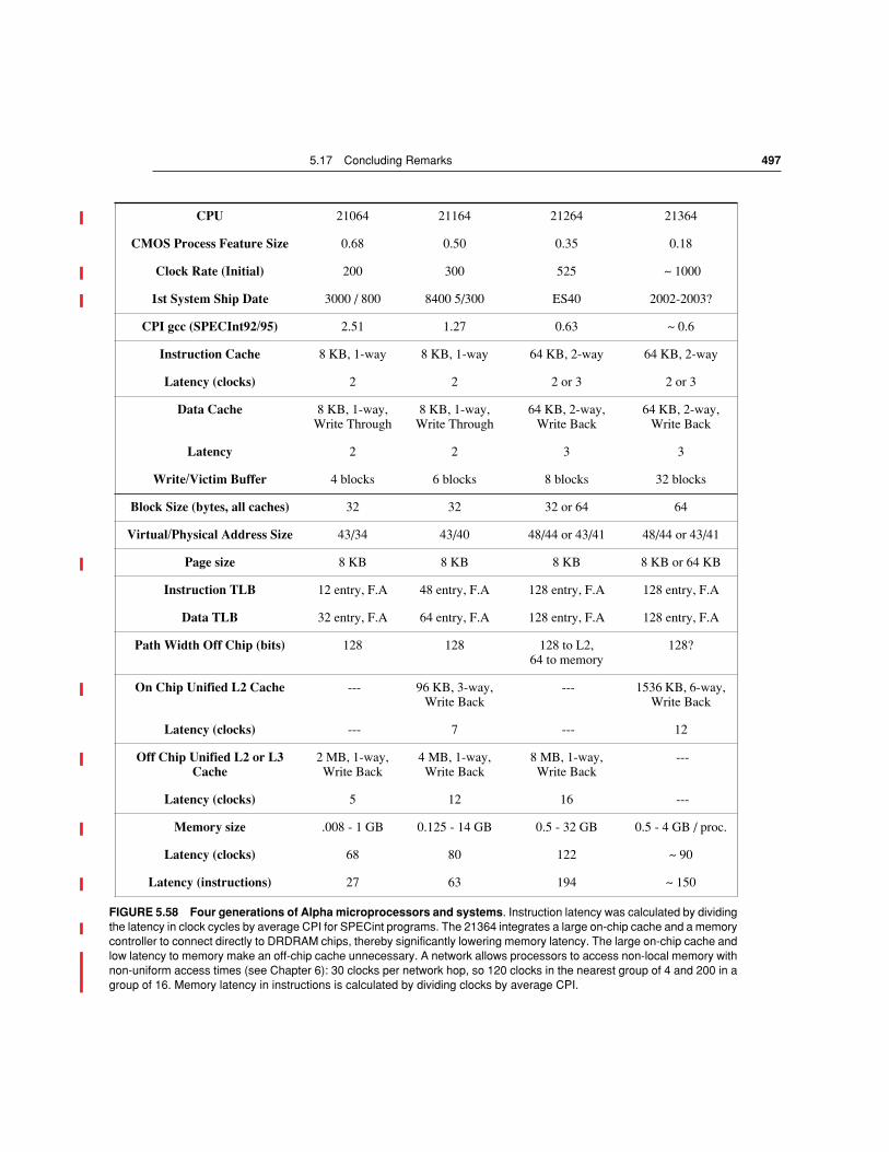
5.17 Concluding Remarks 497
CPU 21064 21164 21264 21364
CMOS Process Feature Size 0.68 0.50 0.35 0.18
Clock Rate (Initial) 200 300 525 ~ 1000
1st System Ship Date 3000 / 800 8400 5/300 ES40 2002-2003?
CPI gcc (SPECInt92/95) 2.51 1.27 0.63 ~ 0.6
Instruction Cache 8 KB, 1-way 8 KB, 1-way 64 KB, 2-way 64 KB, 2-way
Latency (clocks) 2 2 2 or 3 2 or 3
Data Cache 8 KB, 1-way, Write Through
8 KB, 1-way, Write Through
64 KB, 2-way, Write Back
64 KB, 2-way, Write Back
Latency 2 2 3 3
Write/Victim Buffer 4 blocks 6 blocks 8 blocks 32 blocks
Block Size (bytes, all caches) 32 32 32 or 64 64
Virtual/Physical Address Size 43/34 43/40 48/44 or 43/41 48/44 or 43/41
Page size 8 KB 8 KB 8 KB 8 KB or 64 KB
Instruction TLB 12 entry, F.A 48 entry, F.A 128 entry, F.A 128 entry, F.A
Data TLB 32 entry, F.A 64 entry, F.A 128 entry, F.A 128 entry, F.A
Path Width Off Chip (bits) 128 128 128 to L2, 64 to memory
128?
On Chip Unified L2 Cache --- 96 KB, 3-way, Write Back
--- 1536 KB, 6-way, Write Back
Latency (clocks) --- 7 --- 12
Off Chip Unified L2 or L3 Cache
2 MB, 1-way, Write Back
4 MB, 1-way, Write Back
8 MB, 1-way, Write Back
---
Latency (clocks) 5 12 16 ---
Memory size .008 - 1 GB 0.125 - 14 GB 0.5 - 32 GB 0.5 - 4 GB / proc.
Latency (clocks) 68 80 122 ~ 90
Latency (instructions) 27 63 194 ~ 150
FIGURE 5.58 Four generations of Alpha microprocessors and systems. Instruction latency was calculated by dividingthe latency in clock cycles by average CPI for SPECint programs. The 21364 integrates a large on-chip cache and a memorycontroller to connect directly to DRDRAM chips, thereby significantly lowering memory latency. The large on-chip cache andlow latency to memory make an off-chip cache unnecessary. A network allows processors to access non-local memory withnon-uniform access times (see Chapter 6): 30 clocks per network hop, so 120 clocks in the nearest group of 4 and 200 in agroup of 16. Memory latency in instructions is calculated by dividing clocks by average CPI.
498 Chapter 5 Memory-Hierarchy Design
Although the pioneers of computing knew of the need for a memory hierarchyand coined the term, the automatic management of two levels was first proposedby Kilburn et al. [1962]. It was demonstrated with the Atlas computer at theUniversity of Manchester. This computer appeared the year before the IBM 360was announced. Although IBM planned for its introduction with the next genera-tion (System/370), the operating system TSS wasn’t up to the challenge in 1970.Virtual memory was announced for the 370 family in 1972, and it was for thiscomputer that the term “translation look-aside buffer” was coined [Case andPadegs 1978]. The only computers today without virtual memory are a few su-percomputers, embedded processors, and older personal computers.
Both the Atlas and the IBM 360 provided protection on pages, and the GE 645was the first system to provide paged segmentation. The earlier Burroughs com-puters provided virtual memory using segmentation, similar to the segmented ad-dress scheme of the Intel 8086. The 80286, the first 80x86 to have the protectionmechanisms described on pages 463 to 467, was inspired by the Multics protec-tion software that ran on the GE 645. Over time, computers evolved more elabo-rate mechanisms. The most elaborate mechanism was capabilities, whichreached its highest interest in the late 1970s and early 1980s [Fabry 1974; Wulf,Levin, and Harbison 1981]. Wilkes [1982], one of the early workers on capabili-ties, had this to say:
Anyone who has been concerned with an implementation of the type just described [capability system], or has tried to explain one to others, is likely to feel that com-plexity has got out of hand. It is particularly disappointing that the attractive idea of capabilities being tickets that can be freely handed around has become lost .…
Compared with a conventional computer system, there will inevitably be a cost to be met in providing a system in which the domains of protection are small and fre-quently changed. This cost will manifest itself in terms of additional hardware, de-creased runtime speed, and increased memory occupancy. It is at present an open question whether, by adoption of the capability approach, the cost can be reduced to reasonable proportions.
Today there is little interest in capabilities either from the operating systems orthe computer architecture communities, despite growing interest in protectionand security.
Bell and Strecker [1976] reflected on the PDP-11 and identified a small ad-dress space as the only architectural mistake that is difficult to recover from. Atthe time of the creation of PDP-11, core memories were increasing at a very slowrate. In addition, competition from 100 other minicomputer companies meantthat DEC might not have a cost-competitive product if every address had to go
5.18 Historical Perspective and References
5.18 Historical Perspective and References 499
through the 16-bit datapath twice. Hence, the architect's decision to add only 4more address bits than found in the predecessor of the PDP-11.
The architects of the IBM 360 were aware of the importance of address sizeand planned for the architecture to extend to 32 bits of address. Only 24 bits wereused in the IBM 360, however, because the low-end 360 models would have beeneven slower with the larger addresses in 1964. Unfortunately, the architects didn’treveal their plans to the software people, and programmers who stored extra in-formation in the upper 8 “unused” address bit foiled the expansion effort. (Applemade a similar mistake 20 years later with the 24-bit address in the Motorola68000, which required a procedure to later determine “32-bit clean” programs forthe Macintosh when later 68000s used the full 32-bit virtual address.) Virtuallyevery computer since then, will check to make sure the unused bits stay unused,and trap if the bits have the wrong value.
A few years after the Atlas paper, Wilkes published the first paper describingthe concept of a cache [1965]:
The use is discussed of a fast core memory of, say, 32,000 words as slave to a slower core memory of, say, one million words in such a way that in practical cases the effective access time is nearer that of the fast memory than that of the slow memory. [p. 270]
This two-page paper describes a direct-mapped cache. Although this is the firstpublication on caches, the first implementation was probably a direct-mappedinstruction cache built at the University of Cambridge. It was based on tunneldiode memory, the fastest form of memory available at the time. Wilkes statesthat G. Scarott suggested the idea of a cache memory.
Subsequent to that publication, IBM started a project that led to the first com-mercial computer with a cache, the IBM 360/85 [Liptay 1968]. Gibson [1967]describes how to measure program behavior as memory traffic as well as missrate and shows how the miss rate varies between programs. Using a sample of 20programs (each with 3 million references!), Gibson also relied on average memo-ry access time to compare systems with and without caches. This precedent ismore than 30 years old, and yet many used miss rates until the early 1990s.
Conti, Gibson, and Pitkowsky [1968] describe the resulting performance ofthe 360/85. The 360/91 outperforms the 360/85 on only 3 of the 11 programs inthe paper, even though the 360/85 has a slower clock cycle time (80 ns versus60 ns), less memory interleaving (4 versus 16), and a slower main memory(1.04 microsecond versus 0.75 microsecond). This paper was also the first touse the term “cache.”
Others soon expanded the cache literature. Strecker [1976] published thefirst comparative cache design paper examining caches for the PDP-11. Smith[1982] later published a thorough survey paper, using the terms “spatial locali-ty” and “temporal locality”; this paper has served as a reference for many com-puter designers.
500 Chapter 5 Memory-Hierarchy Design
Although most studies relied on simulations, Clark [1983] used a hardwaremonitor to record cache misses of the VAX-11/780 over several days. Clark andEmer [1985] later compared simulations and hardware measurements for transla-tions.
Hill [1987] proposed the three C’s used in section 5.5 to explain cache misses.Jouppi [1998] retrospectively says that Hill’s three Cs model led directly to hisinvention of the victim cache to take advantage of faster direct map caches andyet avoid most of the cost of conflict misses. Ugumar and Abraham' [1993] arguethat the baseline cache for the three C's model should use optimal replacement;this eliminates the anomalies of LRU-based miss classification, and allows con-flict misses to be broken down into those caused by mapping and those caused bya non-optimal replacement algorithm.
One of the first papers on nonblocking caches is by Kroft [1981]. Kroft [1998]later explained that he was the first to design a computer with a cache at ControlData Corporation, and when using old concepts for new mechanisms, he hit uponthe idea of allowing his two-ported cache to continue to service other accesses ona miss.
Baer and Wang [1988] did one of the first examinations of multilevel inclusionproperty. Wang, Baer, and Levy [1989] then produced an early paper on perfor-mance evaluation of multilevel caches. Later, Jouppi and Wilton [1994] proposedmultilevel exclusion for multilevel caches on chip.
In addition to victim caches, Jouppi [1990] also examined prefetching viastreaming buffers. His work was extended by Farkas et al [1995] to that stream-ing buffers work well with non-blocking loads and speculative execution for in-order processors, and later Farkas et al [1997] showed that while out-of-orderprocessors can tolerate unpredictable latency better, they still benefit. They alsorefined memory bandwidth demands of stream buffers.
Proceedings of the Symposium on Architectural Support for Compilers andOperating Systems (ASPLOS) and the International Computer ArchitectureSymposium (ISCA) from the 1990s are filled with papers on caches. (In factsome wags claimed ISCA really stood for the International Cache ArchitectureSymposium.)
This chapter relies on the measurements of SPEC2000 benchmarks collectedby Cantin and Hill [2001]. There are several other papers used in this chapter thatare cited in the captions of the figures that use the data: Agarwal and Pudar[1993]; Barroso, Gharachorloo, and Bugnion [1998]; Farkas and Jouppi [1994];Jouppi [1990]; Lam, Rothberg, and Wolf [1991]; Mowry, Lam, and Gupta[1992]; Lebeck and Wood [1994]; McCalpin [2001]; and Torrellas, Gupta, andHennessy [1992].
The Alpha architecture is described in detail by Bhandarkar [1995] and bySites [1992], and sources of information on the 21264 are Compaq [1999], Cvet-anovic and Kessler [2000], and Kessler[1999]. Two Emotion Engine referencesare Kunimatsu et al [2000] and Oka and Suzuoki [1999]. Information on the SunFire 6800 server is found primarily on Sun’s web site, but Horel and Lauterbach[1999] and Heald, R. et al [2000] published detailed information on UltraSPARCIII.
5.18 Historical Perspective and References 501
References
AGARWAL, A. [1987]. Analysis of Cache Performance for Operating Systems and Multiprogram-ming, Ph.D. Thesis, Stanford Univ., Tech. Rep. No. CSL-TR-87-332 (May).
AGARWAL, A. AND S. D. PUDAR [1993]. “Column-associative caches: A technique for reducing themiss rate of direct-mapped caches,” 20th Annual Int’l Symposium on Computer Architecture ISCA’20, San Diego, Calif., May 16–19. Computer Architecture News 21:2 (May), 179–90.
BAER, J.-L. AND W.-H. WANG [1988]. “On the inclusion property for multi-level cache hierarchies,”Proc. 15th Annual Symposium on Computer Architecture (May–June), Honolulu, 73–80.
Barroso, L.A., Gharachorloo, K. and E. Bugnion [1998]. “Memory System Characterization of Com-mercial Workloads,” Proceedings 25th International Symposium on Computer Architecture, Barce-lona (July), 3-14.
BELL, C. G. AND W. D. STRECKER [1976]. “Computer structures: What have we learned from thePDP-11?,” Proc. Third Annual Symposium on Computer Architecture (January), Pittsburgh, 1–14.
BHANDARKAR, D. P. [1995]. Alpha Architecture Implementations, Digital Press, Newton, Mass.
BORG, A., R. E. KESSLER, AND D. W. WALL [1990]. “Generation and analysis of very long addresstraces,” Proc. 17th Annual Int’l Symposium on Computer Architecture, Seattle, May 28–31, 270–9.
CABTIN, J. F. AND M. D.HILL, [2001]. Cache Performance for Selected SPEC CPU2000 Bench-marks, http://www.jfred.org/cache-data.html, (June).
CASE, R. P. AND A. PADEGS [1978]. “The architecture of the IBM System/370,” Communications ofthe ACM 21:1, 73–96. Also appears in D. P. Siewiorek, C. G. Bell, and A. Newell, Computer Struc-tures: Principles and Examples (1982), McGraw-Hill, New York, 830–855.
CLARK, D. W. [1983]. “Cache performance of the VAX-11/780,” ACM Trans. on Computer Systems1:1, 24–37.
D. W. CLARK and J. S. EMER [1985], “Performance of the VAX-11/780 Translation Buffer: Simu-lation and Measurement,” ACM Trans. on Computer Systems, 3, 1 (February 1985),31-62.
COMPAQ COMPUTER CORPORATION [1999] Compiler Writer's Guide for the Alpha 21264 OrderNumber EC-RJ66A-TE, June, 112 pages. http://www1.support.compaq.com/alpha-tools/documen-tation/current/21264_EV67/ec-rj66a-te_comp_writ_gde_for_alpha21264.pdf
CONTI, C., D. H. GIBSON, AND S. H. PITKOWSKY [1968]. “Structural aspects of the System/360Model 85, Part I: General organization,” IBM Systems J. 7:1, 2–14.
CRAWFORD, J. H. AND P. P. GELSINGER [1987]. Programming the 80386, Sybex, Alameda, Calif.
CVETANOVIC, Z. and R.E. KESSLER [2000] “Performance Analysis of the Alpha 21264-based Com-paq ES40 System.” Proc. 27th Annual Int’l Symposium on Computer Architecture, Vancouver,Canada, June 10-14, IEEE Computer Society Press, 192-202.
FABRY, R. S. [1974]. “Capability based addressing,” Comm. ACM 17:7 (July), 403–412.
Farkas, K.I., P. Chow, N.P. Jouppi,; Z. Vranesic [1997]. “Memory-system design considerations fordynamically-scheduled processors.”24th Annual International Symposium on Computer Architec-ture. Denver, CO, USA, 2-4 June, 133-43.
FARKAS, K. I. AND N. P. JOUPPI [1994]. “Complexity/performance trade-offs with non-blockingloads,” Proc. 21st Annual Int’l Symposium on Computer Architecture, Chicago (April).
Farkas, K.I., N.P.Jouppi, and P. Chow [1995]. “How useful are non-blocking loads, stream buffersand speculative execution in multiple issue processors?,” Proceedings. First IEEE Symposium onHigh-Performance Computer Architecture, Raleigh, NC, USA, 22-25 Jan.,78-89.
GAO, Q. S. [1993]. “The Chinese remainder theorem and the prime memory system,” 20th AnnualInt’l Symposium on Computer Architecture ISCA '20, San Diego, May 16–19, 1993. ComputerArchitecture News 21:2 (May), 337–40.
502 Chapter 5 Memory-Hierarchy Design
GEE, J. D., M. D. HILL, D. N. PNEVMATIKATOS, AND A. J. SMITH [1993]. “Cache performance of theSPEC92 benchmark suite,” IEEE Micro 13:4 (August), 17–27.
GIBSON, D. H. [1967]. “Considerations in block-oriented systems design,” AFIPS Conf. Proc. 30,SJCC, 75–80.
HANDY, J. [1993]. The Cache Memory Book, Academic Press, Boston.
Heald, R. et al [2000]. “ A third-generation SPARC V9 64-b microprocessor,” IEEE Journal of Solid-State Circuits, 35:11 (Nov), 1526-38.
HILL, M. D. [1987]. Aspects of Cache Memory and Instruction Buffer Performance, Ph.D. Thesis,University of Calif. at Berkeley, Computer Science Division, Tech. Rep. UCB/CSD 87/381(November).
HILL, M. D. [1988]. “A case for direct mapped caches,” Computer 21:12 (December), 25–40.
Horel, T. and G. Lauterbach [1999]. “UltraSPARC-III: designing third-generation 64-bit perfor-mance,” IEEE Micro, 19:3 (May-June), 73-85.
Hughes, C.J.; Kaul, P.; Adve, S.V.; Jain, R.; Park, C.; Srinivasan, J. [2001]. “Variability in the execu-tion of multimedia applications and implications for architecture, “ Proc. 28th Annual InternationalSymposium on Computer Architecture, Goteborg, Sweden, 30 June-4 July , 254-65.
JOUPPI, N. P. [1990]. “Improving direct-mapped cache performance by the addition of a small fully-associative cache and prefetch buffers,” Proc. 17th Annual Int’l Symposium on Computer Architec-ture, 364–73.
JOUPPI, N. P. [1998]. “Retrospective: Improving direct-mapped cache performance by the addition ofa small fully-associative cache and prefetch buffers.“25 Years of the International Symposia onComputer Architecture (Selected Papers). ACM, 71-73.
Jouppi, N.P. and S.J.E. Wilton [1994]. “Trade-offs in two-level on-chip caching. Proceedings the 21stAnnual International Symposium on Computer Architecture, Chicago, IL, USA, (18-21 April).34-45.
KESSLER, R.E. [1999] “The Alpha 21264 microprocessor.” IEEE Micro, vol.19, (no.2), March-April,24-36.
KILBURN, T., D. B. G. EDWARDS, M. J. LANIGAN, AND F. H. SUMNER [1962]. “One-level storagesystem,” IRE Trans. on Electronic Computers EC-11 (April) 223–235. Also appears in D. P.Siewiorek, C. G. Bell, and A. Newell, Computer Structures: Principles and Examples (1982),McGraw-Hill, New York, 135–148.
KROFT, D. [1981]. “Lockup-free instruction fetch/prefetch cache organization,” Proc. Eighth AnnualSymposium on Computer Architecture (May 12–14), Minneapolis, 81–87.
KROFT, D. [1998]. “Retrospective: Lockup-Free Instruction Fetch/Prefetch Cache Organization.“25Years of the International Symposia on Computer Architecture (Selected Papers). ACM, 20-21.
KUNIMATSU, A., N. IDE, T. SATO, et al. [2000] “Vector unit architecture for emotion synthesis.” IEEEMicro, vol.20, (no.2), IEEE, March-April, 40-7.
LAM, M. S., E. E. ROTHBERG, AND M. E. WOLF [1991]. “The cache performance and optimizationsof blocked algorithms,” Fourth Int’l Conf. on Architectural Support for Programming Languagesand Operating Systems, Santa Clara, Calif., April 8–11. SIGPLAN Notices 26:4 (April), 63–74.
LEBECK, A. R. AND D. A. WOOD [1994]. “Cache profiling and the SPEC benchmarks: A case study,”Computer 27:10 (October), 15–26.
LIPTAY, J. S. [1968]. “Structural aspects of the System/360 Model 85, Part II: The cache,” IBMSystems J. 7:1, 15–21.
LUK, C.-K. and T.C MOWRY[1999]. “Automatic compiler-inserted prefetching for pointer-based ap-plications.” IEEE Transactions on Computers, vol.48, (no.2), IEEE, Feb. p.134-41.
MCFARLING, S. [1989]. “Program optimization for instruction caches,” Proc. Third Int’l Conf. on
5.18 Historical Perspective and References 503
Architectural Support for Programming Languages and Operating Systems (April 3–6), Boston,183–191.
MCCALPIN, J.D. [2001]. STREAM: Sustainable Memory Bandwidth in High Performance Computershttp://www.cs.virginia.edu/stream/.
MOWRY, T. C., S. LAM, AND A. GUPTA [1992]. “Design and evaluation of a compiler algorithm forprefetching,” Fifth Int’l Conf. on Architectural Support for Programming Languages and OperatingSystems (ASPLOS-V), Boston, October 12–15, SIGPLAN Notices 27:9 (September), 62–73.
OKA, M. and M. SUZUOKI. [1999] “Designing and programming the emotion engine.” IEEE Micro,vol.19, (no.6), Nov.-Dec., 20-8.
PABST, T. [2000], “Performance Showdown at 133 MHz FSB - The Best Platform for Coppermine,”http://www6.tomshardware.com/mainboard/00q1/000302/.
PALACHARLA, S. AND R. E. KESSLER [1994]. “Evaluating stream buffers as a secondary cache re-placement,” Proc. 21st Annual Int’l Symposium on Computer Architecture, Chicago, April 18–21,24–33.
PRZYBYLSKI, S. A. [1990]. Cache Design: A Performance-Directed Approach, Morgan KaufmannPublishers, San Francisco, Calif.
PRZYBYLSKI, S. A., M. HOROWITZ, AND J. L. HENNESSY [1988]. “Performance trade-offs in cachedesign,” Proc. 15th Annual Symposium on Computer Architecture (May–June), Honolulu, 290–298.
REINMAN, G. and N. P. JOUPPI. [1999]. “Extensions to CACTI,” http://research.com-paq.com/wrl/people/jouppi/CACTI.html.
SAAVEDRA-BARRERA, R. H. [1992]. CPU Performance Evaluation and Execution Time PredictionUsing Narrow Spectrum Benchmarking, Ph.D. Dissertation, University of Calif., Berkeley (May).
SAMPLES, A. D. AND P. N. HILFINGER [1988]. “Code reorganization for instruction caches,” Tech.Rep. UCB/CSD 88/447 (October), University of Calif., Berkeley.
SITES, R. L. (ED.) [1992]. Alpha Architecture Reference Manual, Digital Press, Burlington, Mass.
SMITH, A. J. [1982]. “Cache memories,” Computing Surveys 14:3 (September), 473–530.
SMITH, J. E. AND J. R. GOODMAN [1983]. “A study of instruction cache organizations and replace-ment policies,” Proc. 10th Annual Symposium on Computer Architecture (June 5–7), Stockholm,132–137.
STOKES, J. [2000], “Sound and Vision: A Technical Overview of the Emotion Engine,” http://arstech-nica.com/reviews/1q00/playstation2/ee-1.html.
STRECKER, W. D. [1976]. “Cache memories for the PDP-11?,” Proc. Third Annual Symposium onComputer Architecture (January), Pittsburgh, 155–158.
Sugumar, R.A. and S.G. Abraham [1993]. “Efficient simulation of caches under optimal replacementwith applications to miss characterization.” 1993 ACM Sigmetrics Conference on Measurementand Modeling of Computer Systems, Santa Clara, CA, USA, 17-21 May, p.24-35.
TORRELLAS, J., A. GUPTA, AND J. HENNESSY [1992]. “Characterizing the caching and synchron-ization performance of a multiprocessor operating system,” Fifth Int’l Conf. on Architectural Sup-port for Programming Languages and Operating Systems (ASPLOS-V), Boston, October 12–15,SIGPLAN Notices 27:9 (September), 162–174.
WANG, W.-H., J.-L. BAER, AND H. M. LEVY [1989]. “Organization and performance of a two-levelvirtual-real cache hierarchy,” Proc. 16th Annual Symposium on Computer Architecture (May 28–June 1), Jerusalem, 140–148.
WILKES, M. [1965]. “Slave memories and dynamic storage allocation,” IEEE Trans. ElectronicComputers EC-14:2 (April), 270–271.
WILKES, M. V. [1982]. “Hardware support for memory protection: Capability implementations,”
504 Chapter 5 Memory-Hierarchy Design
Proc. Symposium on Architectural Support for Programming Languages and Operating Systems(March 1–3), Palo Alto, Calif., 107–116.
WULF, W. A., R. LEVIN, AND S. P. HARBISON [1981]. Hydra/C.mmp: An Experimental ComputerSystem, McGraw-Hill, New York.
E X E R C I S E S
n Jouppi comments, 2nd pass: drop prime number exercises; mention that “L2misses can be overlapped on 21264 when doing block copies; e.g., overlapreading of source block, writing of destination block. Stream benchmark usesthis; put 21064 on the web, then still use exercise 5.11.
n Reinhart comments, 2nd pass: “In the prefetching section, it might be interest-ing to compare & contrast standard prefetches with the speculative load sup-port found in IA-64 (or maybe this would make a good exercise).”
n Technical reviewer, 2nd pass: Suggests deriving components of accesses to ar-rays X, Y, and Z before and after in blocking example on page 419 to show howcame up with “2N3 + N2 memory words accessed for N3 operations” beforeblocking and “total number of memory words accessed is 2N3/B + N2” after block-ing. (See page 10 of technical review)
n The CACTI program mentioned in the section allows people to design cachesand compare hit times as well as miss rates; I would propose projects that lookat both, or possible use an existing exercise and look at the cache access timesin different technologies: 0.18, 0.13, 0.10 to see how/if the trade-offs differ. Al-so, see how access times differ with different sized caches.
n Jouppi said his teaching experience at Stanford was that it was important toshow a simple in-order CPU so that simple memory performance questionscould be answered using spreadsheets before being exposed to the OOO simu-lators and traces. Thus he suggests saving the 21064 design in some detail andthen include a series of exercises about it so that they can get the ideas herefirst. Perhaps just include a section in the exercises that describes the 21064caches, and keep some of the old exercises?
n To really account for the impact of cache misses on OOO computers, thereneeds to be an OOO instruction simulator to go with the cache. A popular oneis Simple Scalar from Doug Berger, originally from Wisconsin. Another isRSIM from Rice. I’d add the URLs and propose exercises which use them.
n Add a discussion question: given an Out-of-order CPU, how do you quantia-tively evaluate memory options? Why is it different from an in-order CPU?
n Thus these exercises need to be sorted into whether to assume CPU in-order,and can use spreadsheet since it stalls, or out-of-order, and use a simulatorsince you cannot account for overlap. Perhaps can simply look at L2 cache
Exercises 505
misses, assuming L1 are overlapped?
n One advanced exercise (level [25]) is to study the impact of out of order exe-cution on temporal locality in an L1 data cache. The hypothesis is that theremay be more conflict misses due to OOO execution, and that hence multiwayset associativity may be more impact for OOO than for in-order CPUs. Theidea would be to vary out-of-orderness in terms of the size of the load and storequeues and to look at different miss rates as you vary associativity, and see ifthe CPU execution model makes much difference.
n Some of these examples with a short miss time (e.g., next one where miss is10X a hit), state that there is a second level cache and for purposes of this equa-tion assume that it doesn’t miss, hence it makes sense to talk about “small”miss penalties. Real misses all the way to memory should be no less than 100clock cycles
n Mark Hill and Norm Jouppi think we should emphasize “misses per 1000 in-structions” vs. “miss rate” in this edition, so we need several exercises compar-ing them. I intend to replace some of the figures, or show it both ways, so thisshould be supported by exercises using MPI. This is especially true for L2caches, which is much less confusing.
n Next is a great exercise. I’d just change/modernize the numbers so the answersare different. Perhaps make up another one that is similar, just to have somethat aren’t in the answer book?
5.1 [15/15/12/12] <5.1,5.2> Let’s try to show how you can make unfair benchmarks. Hereare two computers with the same processor and main memory but different cache organi-zations. Assume the miss time is 10 times a cache hit time for both computers. Assume writ-ing a 32-bit word takes 5 times as long as a cache hit (for the write-through cache) and thatwriting a whole 32-byte block takes 10 times as long as a cache-read hit (for the write-backcache). The caches are unified; that is, they contain both instructions and data.
Cache A: 128 sets, two elements per set, each block is 32 bytes, and it uses write throughand no-write allocate.
Cache B: 256 sets, one element per set, each block is 32 bytes, and it uses write back anddoes allocate on write misses.
a. [15] <1.5,5.2> Describe a program that makes computer A run as much faster as pos-sible than computer B. (Be sure to state any further assumptions you need, if any.)
b. [15] <1.5,5.2> Describe a program that makes computer B run as much faster as pos-sible than computer A. (Be sure to state any further assumptions you need, if any.)
c. [12] <1.5,5.2> Approximately how much faster is the program in part (a) on computerA than computer B?
d. [12] <1.5,5.2> Approximately how much faster is the program in part (b) on computerB than on computer A?
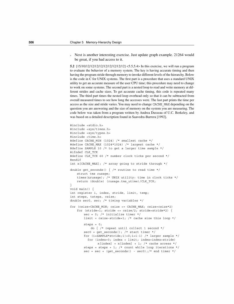
506 Chapter 5 Memory-Hierarchy Design
n Next is another interesting exercise. Just update graph example. 21264 wouldbe great, if you had access to it.
5.2 [15/10/12/12/12/12/12/12/12/12/12] <5.5,5.4> In this exercise, we will run a programto evaluate the behavior of a memory system. The key is having accurate timing and thenhaving the program stride through memory to invoke different levels of the hierarchy. Belowis the code in C for UNIX systems. The first part is a procedure that uses a standard UNIXutility to get an accurate measure of the user CPU time; this procedure may need to changeto work on some systems. The second part is a nested loop to read and write memory at dif-ferent strides and cache sizes. To get accurate cache timing, this code is repeated manytimes. The third part times the nested loop overhead only so that it can be subtracted fromoverall measured times to see how long the accesses were. The last part prints the time peraccess as the size and stride varies. You may need to change CACHE_MAX depending on thequestion you are answering and the size of memory on the system you are measuring. Thecode below was taken from a program written by Andrea Dusseau of U.C. Berkeley, andwas based on a detailed description found in Saavedra-Barrera [1992].
#include <stdio.h>#include <sys/times.h>#include <sys/types.h>#include <time.h>#define CACHE_MIN (1024) /* smallest cache */#define CACHE_MAX (1024*1024) /* largest cache */#define SAMPLE 10 /* to get a larger time sample */#ifndef CLK_TCK#define CLK_TCK 60 /* number clock ticks per second */#endifint x[CACHE_MAX]; /* array going to stride through */
double get_seconds() { /* routine to read time */struct tms rusage;times(&rusage); /* UNIX utility: time in clock ticks */return (double) (rusage.tms_utime)/CLK_TCK;
}void main() {int register i, index, stride, limit, temp;int steps, tsteps, csize;double sec0, sec; /* timing variables */
for (csize=CACHE_MIN; csize <= CACHE_MAX; csize=csize*2) for (stride=1; stride <= csize/2; stride=stride*2) {
sec = 0; /* initialize timer */limit = csize-stride+1; /* cache size this loop */
steps = 0;do { /* repeat until collect 1 second */
sec0 = get_seconds(); /* start timer */for (i=SAMPLE*stride;i!=0;i=i-1) /* larger sample */ for (index=0; index < limit; index=index+stride)
x[index] = x[index] + 1; /* cache access */steps = steps + 1; /* count while loop iterations */sec = sec + (get_seconds() - sec0);/* end timer */
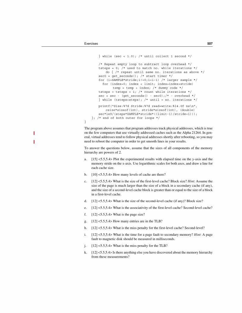
Exercises 507
} while (sec < 1.0); /* until collect 1 second */
/* Repeat empty loop to subtract loop overhead */tsteps = 0; /* used to match no. while iterations */
do { /* repeat until same no. iterations as above */sec0 = get_seconds(); /* start timer */for (i=SAMPLE*stride;i!=0;i=i-1) /* larger sample */ for (index=0; index < limit; index=index+stride)
temp = temp + index; /* dummy code */tsteps = tsteps + 1; /* count while iterations */sec = sec - (get_seconds() - sec0);/* - overhead */} while (tsteps<steps); /* until = no. iterations */
printf("Size:%7d Stride:%7d read+write:%l4.0f ns\n",csize*sizeof(int), stride*sizeof(int), (double)
sec*1e9/(steps*SAMPLE*stride*((limit-1)/stride+1)));}; /* end of both outer for loops */
}
The program above assumes that program addresses track physical addresses, which is trueon the few computers that use virtually addressed caches such as the Alpha 21264. In gen-eral, virtual addresses tend to follow physical addresses shortly after rebooting, so you mayneed to reboot the computer in order to get smooth lines in your results.
To answer the questions below, assume that the sizes of all components of the memoryhierarchy are powers of 2.
a. [15] <5.5,5.4> Plot the experimental results with elapsed time on the y-axis and thememory stride on the x-axis. Use logarithmic scales for both axes, and draw a line foreach cache size.
b. [10] <5.5,5.4> How many levels of cache are there?
c. [12] <5.5,5.4> What is the size of the first-level cache? Block size? Hint: Assume thesize of the page is much larger than the size of a block in a secondary cache (if any),and the size of a second-level cache block is greater than or equal to the size of a blockin a first-level cache.
d. [12] <5.5,5.4> What is the size of the second-level cache (if any)? Block size?
e. [12] <5.5,5.4> What is the associativity of the first-level cache? Second-level cache?
f. [12] <5.5,5.4> What is the page size?
g. [12] <5.5,5.4> How many entries are in the TLB?
h. [12] <5.5,5.4> What is the miss penalty for the first-level cache? Second-level?
i. [12] <5.5,5.4> What is the time for a page fault to secondary memory? Hint: A pagefault to magnetic disk should be measured in milliseconds.
j. [12] <5.5,5.4> What is the miss penalty for the TLB?
k. [12] <5.5,5.4> Is there anything else you have discovered about the memory hierarchyfrom these measurements?
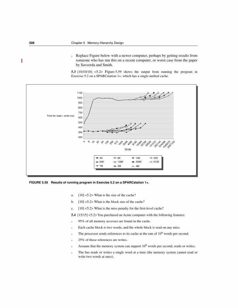
508 Chapter 5 Memory-Hierarchy Design
n Replace Figure below with a newer computer, perhaps by getting results fromsomeone who has run this on a recent computer, or worst case from the paperby Saveerda and Smith.
5.3 [10/10/10] <5.2> Figure 5.59 shows the output from running the program inExercise 5.2 on a SPARCstation 1+, which has a single unified cache.
a. [10] <5.2> What is the size of the cache?
b. [10] <5.2> What is the block size of the cache?
c. [10] <5.2> What is the miss penalty for the first-level cache?
5.4 [15/15] <5.2> You purchased an Acme computer with the following features:
n 95% of all memory accesses are found in the cache.
n Each cache block is two words, and the whole block is read on any miss.
n The processor sends references to its cache at the rate of 109 words per second.
n 25% of those references are writes.
n Assume that the memory system can support 109 words per second, reads or writes.
n The bus reads or writes a single word at a time (the memory system cannot read orwrite two words at once).
FIGURE 5.59 Results of running program in Exercise 5.2 on a SPARCstation 1+.
1100
4 8 16 32 64 128
256
512
1024
2048
4096
8192
1638
4
3276
8
6553
6
1310
72
2621
44
5242
88
1048
576
2097
152
1000
900
800
700
600
500
400
300
200
4K
64K
8K
128K
2M1M
16K
Stride
256K
4M
32K
512K
Time for read + write (ns)
Exercises 509
n Assume at any one time, 30% of the blocks in the cache have been modified.
n The cache uses write allocate on a write miss.
You are considering adding a peripheral to the system, and you want to know how much ofthe memory system bandwidth is already used. Calculate the percentage of memory systembandwidth used on the average in the two cases below. Be sure to state your assumptions.
a. [15] <5.2> The cache is write through.
b. [15] <5.2> The cache is write back.
5.5 [15/15] <5.7> One difference between a write-through cache and a write-back cachecan be in the time it takes to write. During the first cycle, we detect whether a hit will occur,and during the second (assuming a hit) we actually write the data. Let’s assume that 50%of the blocks are dirty for a write-back cache. For this question, assume that the write bufferfor write through will never stall the CPU (no penalty). Assume a cache read hit takes 1clock cycle, the cache miss penalty is 50 clock cycles, and a block write from the cache tomain memory takes 50 clock cycles. Finally, assume the instruction cache miss rate is 0.5%and the data cache miss rate is 1%.
a. [15] <5.7> Using statistics for the average percentage of loads and stores from MIPSin Figure 2.32 on page 149, estimate the performance of a write-through cache with atwo-cycle write versus a write-back cache with a two-cycle write for each of theprograms.
b. [15] <5.7> Do the same comparison, but this time assume the write-through cachepipelines the writes, so that a write hit takes just one clock cycle.
5.6 [20] <5.5> Improve on the compiler prefetch Example found on page 425: Try to elim-inate both the number of extraneous prefetches and the number of non-prefetched cachemisses. Calculate the performance of this refined version using the parameters in theExample.
n The following example isn’t there any more
5.7 [15/12] <5.5> The example evaluation of a pseudo-associative cache on page 399assumed that on a hit to the slower block the hardware swapped the contents with the cor-responding fast block so that subsequent hits on this address would all be to the fast block.Assume that if we don’t swap, a hit in the slower block takes just one extra clock cycle in-stead of two extra clock cycles.
a. [15] <5.5> Derive a formula for the average memory access time using the terminol-ogy for direct-mapped and two-way set-associative caches as given on page 399.
b. [12] <5.5> Using the formula from part (a), recalculate the average memory accesstimes for the two cases found on page 399 (8-KB cache and 256-KB cache). Whichpseudo-associative scheme is faster for the given configurations and data?
n Perhaps next is a good in-order v. out-of-order exercise?
5.8 [15/20/15] <5.10> If the base CPI with a perfect memory system is 1.5, what is the CPIfor these cache organizations? Use Figure 5.14 (page 409):
n 16-KB direct-mapped unified cache using write back.
510 Chapter 5 Memory-Hierarchy Design
n 16-KB two-way set-associative unified cache using write back.
n 32-KB direct-mapped unified cache using write back.
Assume the memory latency is 40 clocks, the transfer rate is 4 bytes per clock cycle andthat 50% of the transfers are dirty. There are 32 bytes per block and 20% of the instructionsare data transfer instructions. There is no write buffer. Add to the assumptions above a TLBthat takes 20 clock cycles on a TLB miss. A TLB does not slow down a cache hit. For theTLB, make the simplifying assumption that 0.2% of all references aren’t found in TLB,either when addresses come directly from the CPU or when addresses come from cachemisses.
a. [15] <5.5> Compute the effective CPI for the three caches assuming an ideal TLB.
b. [20] <5.5> Using the results from part (a), compute the effective CPI for the threecaches with a real TLB.
c. [15] <5.5> What is the impact on performance of a TLB if the caches are virtually orphysically addressed?
5.9 [10] <5.4> What is the formula for average access time for a three-level cache?
n prime number of memory banks were dropped for the 3/e. Thus we must mod-ify Exercise 5.10 which refers to the prime number of banks, at least to explainthe ideas. Perhaps even add exercises, including an explanation of the ideasdropped from the second edition by using text from the second edition?
5.10 [15/15] <5.8> The section on avoiding bank conflicts by having a prime number ofmemory banks mentioned that there are techniques for fast modulo arithmetic, especiallywhen the prime number can be represented as 2N – 1. The idea is that by understanding thelaws of modulo arithmetic we can simplify the hardware. The key insights are the following:
1. Modulo arithmetic obeys the laws of distribution:
((a modulo c) + (b modulo c)) modulo c = (a + b) modulo c((a modulo c) × (b modulo c)) modulo c = (a × b) modulo c
2. The sequence 20 modulo 2N– 1, 21 modulo 2N– 1, 22 modulo 2N– 1, . . . is a repeatingpattern 20, 21, 22, and so on for powers of 2 less than 2N. For example, if 2N– 1 = 7, then
20 modulo 7 = 121 modulo 7 = 222 modulo 7 = 423 modulo 7 = 124 modulo 7 = 225 modulo 7 = 4
3. Given a binary number a, the value of (a mod 7) can be expressed as
ai × 2i +. . .+ a2 × 22 + a1 × 21 + a0 × 20 modulo 7 =((a0 + a3 +. . .) × 1 + (a1 + a4 +. . .) × 2 + (a2 + a5 +…) × 4) modulo 7
where i = log2a and aj = 0 for j >i
This is possible because 7 is a prime number of the form 2N–1. Since the multiplica-
Exercises 511
tions in the expression above are by powers of two, they can be replaced by binaryshifts (a very fast operation).
4. The address is now small enough to find the modulo by looking it up in a read-onlymemory (ROM) to get the bank number.
Finally, we are ready for the questions.
a. [15] <5.8> Given 2N– 1 memory banks, what is the approximate reduction in size ofan address that is M bits wide as a result of the intermediate result in step 3 above?Give the general formula, and then show the specific case of N = 3 and M = 32.
b. [15] <5.8> Draw the block structure of the hardware that would pick the correct bankout of seven banks given a 32-bit address. Assume that each bank is 8 bytes wide.What is the size of the adders and ROM used in this organization?
n Old, so drop?
5.11 [25/10/15] <5.8> The CRAY X-MP instruction buffers can be thought of as an in-struction-only cache. The total size is 1 KB, broken into four blocks of 256 bytes per block.The cache is fully associative and uses a first-in, first-out replacement policy. The accesstime on a miss is 10 clock cycles, with the transfer time of 64 bytes every clock cycle. TheX-MP takes 1 clock cycle on a hit. Use the cache simulator to determine the following:
a. [25] <5.8> Instruction miss rate.
b. [10] <5.8> Average instruction memory access time measured in clock cycles.
c. [15] <5.8> What does the CPI of the CRAY X-MP have to be for the portion due toinstruction cache misses to be 10% or less?
n The next 5 exercises all refer to traces. Since we no longer have traces readilyavailable, these exercises should be changed to work with something like Burg-er’s simulator running a program and producing addresses vs. an address trace,unless there are some traces left online someplace?
5.12 [25] <5.8> Traces from a single process give too high estimates for caches used in amultiprocess environment. Write a program that merges the uniprocess DLX traces into asingle reference stream. Use the process-switch statistics in Figure 5.25 (page 432) as theaverage process-switch rate with an exponential distribution about that mean. (Use thenumber of clock cycles rather than instructions, and assume the CPI of DLX is 1.5.) Usethe cache simulator on the original traces and the merged trace. What is the miss rate foreach, assuming a 64-KB direct-mapped cache with 16-byte blocks? (There is a process-identified tag in the cache tag so that the cache doesn’t have to be flushed on each switch.)
5.13 [25] <5.8> One approach to reducing misses is to prefetch the next block. A simplebut effective strategy, found in the Alpha 21064, is when block i is referenced to make sureblock i + 1 is in the cache, and if not, to prefetch it. Do you think automatic prefetching ismore or less effective with increasing block size? Why? Is it more or less effective with in-creasing cache size? Why? Use statistics from the cache simulator and the traces to supportyour conclusion.
5.14 [20/25] <5.8> Smith and Goodman [1983] found that for a small instruction cache, a
512 Chapter 5 Memory-Hierarchy Design
cache using direct mapping could consistently outperform one using fully associative withLRU replacement.
a. [20] <5.8> Explain why this would be possible. (Hint: You can’t explain this with thethree C’s model because it ignores replacement policy.)
b. [25] <5.8> Use the cache simulator to see if their results hold for the traces.
5.15 [30] <5.10> Use the cache simulator and traces to calculate the effectiveness of a four-bank versus eight-bank interleaved memory. Assume each word transfer takes one clock onthe bus and a random access is eight clocks. Measure the bank conflicts and memory band-width for these cases:
a. <5.10> No cache and no write buffer.
b. <5.10> A 64-KB direct-mapped write-through cache with four-word blocks.
c. <5.10> A 64-KB direct-mapped write-back cache with four-word blocks.
d. <5.10> A 64-KB direct-mapped write-through cache with four-word blocks but the“interleaving” comes from a page-mode DRAM.
e. <5.10> A 64-KB direct-mapped write-back cache with four-word blocks but the “in-terleaving” comes from a page-mode DRAM.
5.16 [25/25/25] <5.10> Use a cache simulator and traces to calculate the effectiveness ofearly restart and out-of-order fetch. What is the distribution of first accesses to a block asblock size increases from 2 words to 64 words by factors of two for the following:
a. [25] <5.10> A 64-KB instruction-only cache?
b. [25] <5.10> A 64-KB data-only cache?
c. [25] <5.10> A 128-KB unified cache?
Assume direct-mapped placement.
5.17 [25/25/25/25/25/25] <5.2> Use a cache simulator and traces with a program you writeyourself to compare the effectiveness of these schemes for fast writes:
a. [25] <5.2> One-word buffer and the CPU stalls on a data-read cache miss with a write-through cache.
b. [25] <5.2> Four-word buffer and the CPU stalls on a data-read cache miss with awrite-through cache.
c. [25] <5.2> Four-word buffer and the CPU stalls on a data-read cache miss only if thereis a potential conflict in the addresses with a write-through cache.
d. [25] <5.2> A write-back cache that writes dirty data first and then loads the missedblock.
e. [25] <5.2> A write-back cache with a one-block write buffer that loads the miss datafirst and then stalls the CPU on a clean miss if the write buffer is not empty.
f. [25] <5.2> A write-back cache with a one-block write buffer that loads the miss datafirst and then stalls the CPU on a clean miss only if the write buffer is not empty and
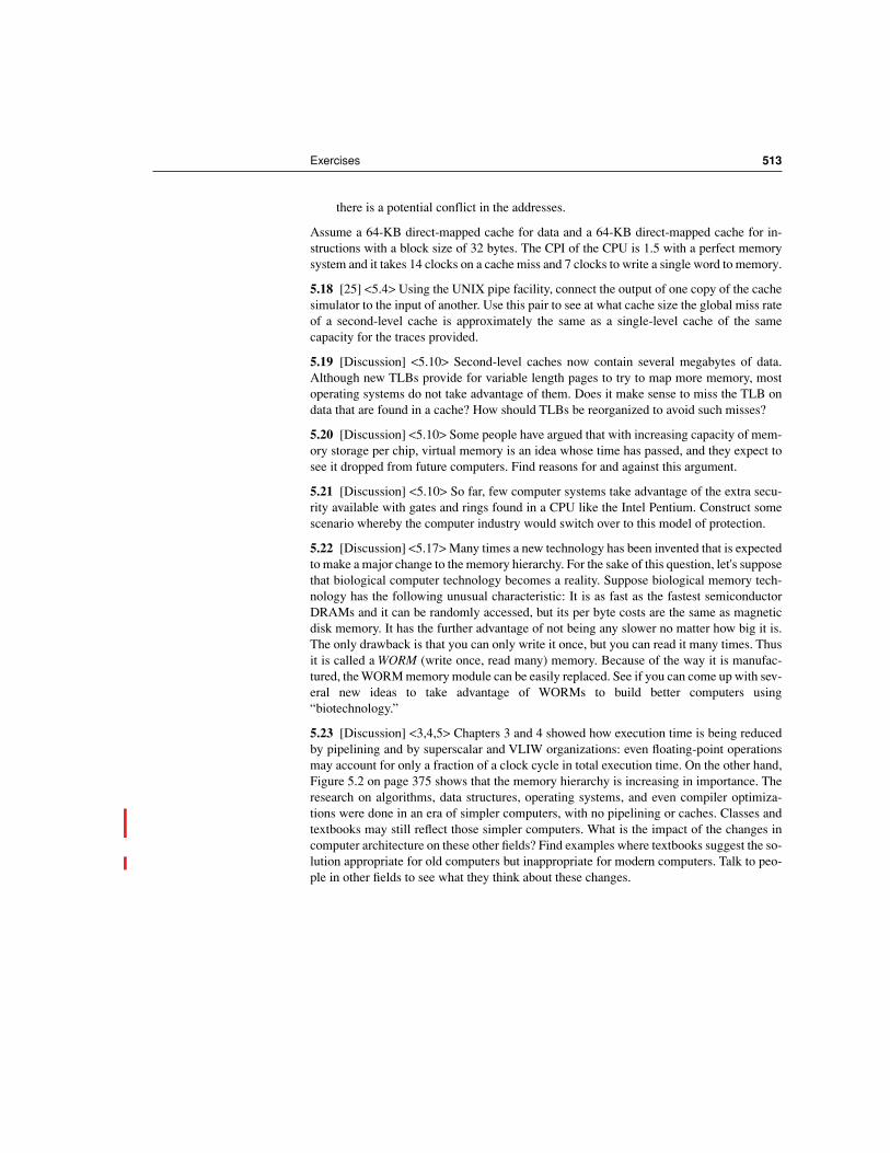
Exercises 513
there is a potential conflict in the addresses.
Assume a 64-KB direct-mapped cache for data and a 64-KB direct-mapped cache for in-structions with a block size of 32 bytes. The CPI of the CPU is 1.5 with a perfect memorysystem and it takes 14 clocks on a cache miss and 7 clocks to write a single word to memory.
5.18 [25] <5.4> Using the UNIX pipe facility, connect the output of one copy of the cachesimulator to the input of another. Use this pair to see at what cache size the global miss rateof a second-level cache is approximately the same as a single-level cache of the samecapacity for the traces provided.
5.19 [Discussion] <5.10> Second-level caches now contain several megabytes of data.Although new TLBs provide for variable length pages to try to map more memory, mostoperating systems do not take advantage of them. Does it make sense to miss the TLB ondata that are found in a cache? How should TLBs be reorganized to avoid such misses?
5.20 [Discussion] <5.10> Some people have argued that with increasing capacity of mem-ory storage per chip, virtual memory is an idea whose time has passed, and they expect tosee it dropped from future computers. Find reasons for and against this argument.
5.21 [Discussion] <5.10> So far, few computer systems take advantage of the extra secu-rity available with gates and rings found in a CPU like the Intel Pentium. Construct somescenario whereby the computer industry would switch over to this model of protection.
5.22 [Discussion] <5.17> Many times a new technology has been invented that is expectedto make a major change to the memory hierarchy. For the sake of this question, let's supposethat biological computer technology becomes a reality. Suppose biological memory tech-nology has the following unusual characteristic: It is as fast as the fastest semiconductorDRAMs and it can be randomly accessed, but its per byte costs are the same as magneticdisk memory. It has the further advantage of not being any slower no matter how big it is.The only drawback is that you can only write it once, but you can read it many times. Thusit is called a WORM (write once, read many) memory. Because of the way it is manufac-tured, the WORM memory module can be easily replaced. See if you can come up with sev-eral new ideas to take advantage of WORMs to build better computers using“biotechnology.”
5.23 [Discussion] <3,4,5> Chapters 3 and 4 showed how execution time is being reducedby pipelining and by superscalar and VLIW organizations: even floating-point operationsmay account for only a fraction of a clock cycle in total execution time. On the other hand,Figure 5.2 on page 375 shows that the memory hierarchy is increasing in importance. Theresearch on algorithms, data structures, operating systems, and even compiler optimiza-tions were done in an era of simpler computers, with no pipelining or caches. Classes andtextbooks may still reflect those simpler computers. What is the impact of the changes incomputer architecture on these other fields? Find examples where textbooks suggest the so-lution appropriate for old computers but inappropriate for modern computers. Talk to peo-ple in other fields to see what they think about these changes.


![CS 104 Computer Organization and Design...Computer Organization and Design Memory Hierarchy CS104: Memory Hierarchy [Adapted from A. Roth] 2 Memory Hierarchy • Basic concepts •](https://img.pdfslide.us/doc/110x75/60a6b4852c2f420e7342dd30/cs-104-computer-organization-and-design-computer-organization-and-design-memory.jpg)