Embed Size (px)
Citation preview

1
5 Computer Architecture1
This chapter is the pinnacle of the hardware part of our journey. We are now ready to take all
the chips that we’ve built in chapters 1–3 and integrate them into a general-purpose computer
system capable of running programs written in the machine language presented in chapter 4.
The specific computer we will build, called Hack, has two important virtues. On the one hand,
Hack is a simple machine that can be constructed in just a few hours, using previously built
chips and the hardware simulator supplied with the book. On the other hand, Hack is
sufficiently powerful to illustrate the key operating principles and hardware elements of any
general-purpose computer. Therefore, building it will give you an excellent understanding of
how modern computers work at the low hardware and software levels.
Section 5.1 begins with an overview of the von Neumann architecture — a central
dogma in computer science underlying the design of almost all modern computers. The Hack
platform is a von Neumann machine variant, and section 5.2 gives its exact hardware
specification. Section 5.3 describes how the Hack platform can be implemented from previously
built chips, in particular the ALU built in project 2 and the registers and memory systems built
in project 3. Section 5.4 compares the Hack machine with industrial-strength computers, and
emphasizes the critical role that optimization plays in the latter. Section 5.5 gives an overview
of the computer construction project.
The computer that will emerge from this project will be as simple as possible, but not
simpler. On the one hand, the computer will be based on a minimal and compact hardware
configuration. On the other hand, this configuration will be sufficiently powerful for executing
programs written in a Java-like programming language, delivering a reasonable performance
and a satisfying user experience. 1 Chapter 5 from The Elements of Computing Systems by Noam Nisan and Shimon Schocken, Second Edition, MIT Press, forthcoming 2017.

2
5.1 Computer Architecture Fundamentals
5.1.1 The Stored Program Concept
Compared to all the other machines around us, the most unique feature of the digital computer
is its amazing versatility. Here is a machine with finite hardware that can perform an infinite
number of tasks, from playing games to publishing books to designing airplanes. This
remarkable versatility—a boon that we have come to take for granted—is the fruit of a brilliant
idea called the stored program concept. Formulated independently by several scientists and
engineers in the 1930s, the stored program concept is still considered the most profound
invention in, if not the very foundation of, modern computer science.
Like many scientific breakthroughs, the basic idea is remarkably simple. The computer
is based on a fixed hardware platform, capable of executing a fixed repertoire of very simple
instructions. At the same time, these instructions can be combined like building blocks, yielding
arbitrarily sophisticated programs. Moreover, the logic of these programs is not embedded in
the hardware, as it was in mechanical computers predating 1930. Instead, the program’s code is
temporarily stored and manipulated in the computer’s memory, just like data, becoming what is
known as “software.” Since the computer’s operation manifests itself to the user through the
currently executing software, the same hardware platform can be made to behave completely
differently each time it is loaded with a different program.
5.1.2 The von Neumann Architecture
The stored program concept is a key element of many abstract and practical computer models,
most notably the universal Turing machine (1936) and the von Neumann machine (1945). The
Turing machine—an abstract artifact describing a deceptively simple computer—is used mainly
in theoretical computer science, for analyzing the logical foundations of computational

3
problems and solutions. In contrast, the von Neumann machine is a practical architecture and
the conceptual blueprint of almost all computer platforms today.
The von Neumann architecture, shown in diagram 5.1, is based on a central processing
unit (CPU), interacting with a memory device, receiving data from some input device, and
sending data to some output device. At the heart of this architecture lies the stored program
concept: The computer’s memory stores not only the data that the computer manipulates, but
also the very instructions that tell the computer what to do. Let us explore this architecture in
some detail.
Diagram 5.1: the von Neumann architecture

4
5.1.3 Memory
Like other hardware elements, the memory unit can be discussed from a physical perspective
and from a logical perspective. Physically, the memory is a linear sequence of addressable
registers, each having a unique address and a value, which is a fixed-size word of information.
Logically, the memory is divided into two areas. One area is dedicated for storing data, e.g. the
arrays and objects of programs that are presently executing, while the other area is dedicated for
storing the programs’ instructions. Although all these “data words” and “instruction words”
look exactly the same physically, they serve very different purposes.
In some von Neumann architecture variants, the data memory and the instruction memory
are managed within the same physical memory unit, as was just explained. In other variants, the
data memory and the instruction memory are kept in separate physical memory units that have
distinct address spaces. This setting, sometimes referred to as ”Harvard architecture”, is also the
architecture of our Hack computer. Both variants have certain advantages that will be discussed
later in the chapter.
All the memory registers—irrespective of their roles—are accessed in the same way: in
order to manipulate a particular memory register, one must first select the register by supplying
an address. This action provides an immediate access to the register’s data. The term Random
Access Memory (RAM) is often used to denote the important fact that each randomly selected
register can be reached in the same access time, irrespective of the memory size and the
register’s location in it.
Data Memory: High-level programs manipulate abstract artifacts like variables, arrays, and
objects. After the programs are translated into machine language, these data abstractions
become binary codes, stored in the computer’s memory. Once an individual register has been
5
selected from the memory by specifying its address, its contents can be either read or written to.
In the former case, we retrieve the value of the selected register. In the latter case, we store a
new value in the selected register, overriding the previous value. Such memories are sometimes
referred to as “read/write” memories.
Instruction Memory: Before high-level programs can be executed on the computer, they must
be translated into machine language. Following this translation, each high-level statement
becomes a series of one or more machine language instructions. These instructions are stored in
the computer’s instruction memory as binary codes. In each step of a program’s execution, the
CPU fetches (i.e., reads) a binary machine instruction from a selected register in the instruction
memory, decodes it, executes the specified instruction, and figures out which instruction to
fetch and execute next.
We see that before executing a particular program, we must first load the program’s code
into the instruction memory, typically from some peripheral mass storage device like a disk.
Given the compact and highly focused perspective of a von Neumann machine, how a program
is loaded into the computer’s instruction memory is considered an external issue. What’s
important is that when the CPU is called upon to execute a program, the program’s code will
already reside in memory, one way or another. As you saw in chapter 4, the act of loading a
program into the instruction memory from an external text file is supported by the supplied
CPU emulator.
5.1.4 Central Processing Unit
The CPU—the centerpiece of the computer’s architecture—is in charge of executing the
instructions of the currently loaded program. These instructions tell the CPU which calculation
it has to perform, which registers is has to read from or write to, and which instruction it has to
fetch and execute next. The CPU executes these tasks using three main hardware elements: an
Arithmetic-Logic Unit (ALU), a set of registers, and a control unit.

6
Arithmetic Logic Unit: The ALU chip is built to perform all the low-level arithmetic and
logical operations featured by the computer. For example, a typical ALU can add two numbers,
compute a bitwise And function on two numbers, compare two numbers, and so on. How much
functionality an ALU should have is a matter of need, budget, energy, and similar cost-
effectiveness considerations. Any function not supported by the ALU as a primitive hardware
operation can be later realized by the computer’s system software (yielding a slower
implementation, of course).
Registers: Since the CPU is the computer’s centerpiece, it must perform as efficiently as
possible. In order to boost performance, it is desirable to store the intermediate results that
computer programs generate locally, close to the ALU, rather than ship them in and out of the
CPU chip and store them in some remote and separate RAM chip. Thus, a CPU is typically
equipped with a small set of 2 up to 32 resident high-speed registers, each capable of holding a
single word.
Control Unit: A computer instruction is represented as a binary code, typically 16, 32, or 64
bits wide. Before such an instruction can be executed, it must be decoded, and the information
embedded in it must be used to signal various hardware devices (ALU, registers, memory) how
to execute the instruction. The instruction decoding is done by some control unit, which is also
responsible for figuring out which instruction to fetch and execute next.
The CPU operation can now be described as a repeated loop: decode the current
instruction, execute it, figure out which instruction to execute next, fetch it, decode it, and so on.
This process is sometimes referred to as the “fetch-execute cycle”.
5.1.5 Registers
When talking about computer hardware, the term “register” is used quite liberally to refer to any
device capable of storing a chunk of bits that represents some stand-alone value like a variable

7
value, an instruction, or an address. According to this broad definition, any memory location is
in fact a register, and so of course are the registers that reside inside the CPU. This section is
dedicated to a discussion of these CPU-resident registers.
Suppose we didn’t have any CPU-resident registers. This would imply that any CPU
operation that requires inputs or outputs would have to rely on memory access. Let us consider
what each such memory access entails. First, some address value travels from the CPU to the
RAM’s address input. Next, the RAM’s direct-access logic uses the supplied address to select a
specific memory register. Finally, the register’s contents either travels back to the CPU (a read
operation), or is replaced by some additional value that travels from the CPU (a write operation).
Note that this elaborate process involves at least two separate chips, an address bus, and a
data bus, resulting in an expensive and time-consuming operation. This stands in sharp contract
to the ALU, which is a lean and mean combinational machine. Thus we have a lightning fast
calculator that depends on a sluggish data store for supplying inputs and consuming outputs.
The result may well lead to what is sometimes called starvation, which is what happens when a
processor is denied the resources it needs to complete its work.
Clearly, if we could have placed a few high-speed registers inside the CPU itself, right
next to the ALU, we could have saved ourselves a great deal of time and overhead. There is
another, subtle but critically important advantage for using CPU-resident registers. In order to
specify an instruction that includes a memory register, like Memory[addr]=value, we must
supply a memory address, which typically requires many bits. In the 16-bit Hack platform, this
technical detail alone forces us to use two machine instructions, and two clock cycles, even for
preforming mundane tasks like Memory[addr]=0 or Memory[addr]=1.
In contrast, since there are normally only a few CPU-resident registers, identifying each
one of them requires only a few bits. Therefore, an operation like someCPURegister=0 or

8
someCPURegister=1 requires only one machine instruction, and one cycle. To sum up, CPU-
resident registers save unnecessary memory access, and allow using thinner instruction formats,
resulting in faster throughput. The remainder of this section describes the registers that CPU’s
typically use.
Data registers: These registers give the CPU short-term memory services. For example, if a
program wants to calculate (a − b) ⋅ c, we must first compute and remember the value of (a − b).
In principle, this temporary result can be stored in some memory register. Clearly, a much more
sensible solution is to store it locally inside the CPU, using a data register. Typically, CPU’s
use at least one and up to 32 data registers.
Address registers: Many machine language instructions involve memory access: reading data,
writing data, and fetching instructions. In any one of these operations, we must specify which
memory register we wish to operate on. This is done by supplying an address. In some cases,
the address is coded as part of the instruction, while in other cases the address is specified, or
computed, by some previous instruction. In the latter case, the address must be stored
somewhere. This is done using a CPU-resident chip called address register.
Unlike regular registers, the output of an address register is typically connected to the
address input of a memory device. Therefore, placing a value in the address register has the side
effect of selecting a particular memory register, and this register makes itself available to
subsequent instructions designed to manipulate it. For example, suppose we wish to set
Memory[17] to 1. In the Hack language, this can be done using the pair of instructions @17
(which sets A=17 and makes the M mnemonic stand for Memory[17]), followed by M=1 (which
sets the selected memory register to 1).
In addition to supporting this fundamental addressing operation, an address register is,
well, a register. Therefore, if needed, it can be used as yet another data register. For example,

9
suppose we wish to set the D register to 17. This can be done using the pair of instructions @17,
followed by D=A. Here we use A not as an address register, but rather as a data register. The fact
that Memory[17] was selected as a side effect of @17 is completely ignored.
Program counter: When executing a program, the CPU must always keep track of the address
of the instruction that must be fetched and executed next. This address is kept in a special
register called program counter, or PC. The contents of the PC is computed and updated as a
side effect of executing the current instruction, as we elaborate later in the chapter.
5.1.6 Input and Output
Computers interact with their external environments using a diverse array of input and output
(I/O) devices. These include screens, keyboards, disks, printers, scanners, network interface
cards, and so on, not to mention the bewildering array of proprietary components that embedded
computers are called to control in automobiles, cameras, medical devices, and so on. There are
two reasons why we don’t concern ourselves here with the low-level architecture of these
various devices. First, every one of them represents a unique piece of machinery requiring a
unique knowledge of engineering. Second, and for this very same reason, computer scientists
have devised clever schemes to make all these different devices look exactly the same to the
computer. The key trick in managing this complexity is called memory-mapped I/O.
The basic idea is to create a binary emulation of the I/O device, making it “look” to the
CPU as if it were a regular memory segment. In particular, each I/O device is allocated an
exclusive area in memory, becoming its “memory map.” In the case of an input device like a
keyboard, the memory map is made to continuously reflect the physical state of the device:
when the user presses a key on the keyboard, a binary code representing that key appears in the
keyboard’s memory map. In the case of an output device like a screen, the screen is made to
continuously reflect the state of its designated memory map: when we write a bit in the screen’s

10
memory map, a certain pixel turns on or off on the screen. The I/O devices are “refreshed” from
the memory (and vice versa) several times per second, so the response time from the user’s
perspective is almost instantaneous. Programmatically, the key implication is that computer
programs can access any I/O device by simply manipulating selected registers in their
designated memory areas.
Obviously, this arrangement is based on several agreed-upon contracts. First, the data that
drives each I/O device must be serialized, or “mapped”, on the computer’s memory, hence the
name “memory map”. For example, the screen, which can be viewed as a 2-dimensional grid of
pixels, must be mapped on a 1-dimensional vector of fixed-size memory registers. Second, each
I/O device is required to support some agreed-upon interaction protocol, so that programs will
be able to access it in a predictable manner. For example, it should be decided, and agreed-upon,
which binary codes should represent which keys on the keyboard. As a side comment, given the
multitude of computer platforms, I/O devices, and different hardware and software vendors, one
can appreciate the crucial role that standards play in determining these low-level interaction
contracts.
The practical implications of a memory-mapped I/O architecture are significant: The
design of the CPU and the overall platform can be totally independent of the number, nature, or
make of the I/O devices that interact, or will interact, with the computer. Whenever we want to
connect a new I/O device to the computer, all we have to do is allocate to it a new memory map
and “take note” of its base address (these one-time configurations are typically done by the
operating system). From this point onward, any program that wants to manipulate this I/O
device can do so—all it needs to do is manipulate selected registers in the memory map
designated to represent the device.

11
The architectural framework described thus far in the chapter is characteristic of any general-
purpose computer system. We now turn to describe one specific example of this architecture:
the Hack computer.
5.2 The Hack Hardware Platform: Specification
5.2.1 Overview
The Hack platform is a 16-bit von Neumann machine, designed to execute programs written in
the Hack machine language presented in chapter 4. In order to do so, the Hack platform consists
of a CPU, two separate memory modules serving as instruction memory and data memory, and
two memory-mapped I/O devices: a screen and a keyboard.
The Hack computer executes programs that reside in an instruction memory. In physical
implementations of the Hack platform, this memory can be implemented using a ROM chip that
is pre-loaded with the required program. Software-based simulators of the Hack computer are
expected to support this functionality by providing means for loading the instruction memory
from a text file containing a program written in the Hack machine language.
The Hack CPU consists of the ALU built in project 2 and three registers called data
register (D), address register (A), and program counter (PC), identical to the 16-bit registers
built in project 3. While the D-register is used solely for storing data values, the A-register serves
three different purposes, depending on the context in which it is used: storing a data value (just
like the D-register), pointing at an address in the instruction memory, or pointing at an address
in the data memory. More about this, later.
The Hack CPU is designed to execute instructions written in the Hack machine language.
These instructions have the 16-bit format “ixxaccccccdddjjj”. The i-bit (also known as
opcode) codes the instruction type, which is either 0 for an A-instruction or 1 for a C-instruction.
In case of an A-instruction, the instruction is treated as a 16-bit binary value which is loaded

12
into the A register. In case of a C-instruction, the instruction is treated as a sequence of control
bits that determine which function the ALU should computer, and in which registers the
computed value should be stored. In the course of executing any one of these instructions, the
CPU also figures out which instruction in the program should be fetched and executed next.
We now turn to specify the various components of the Hack hardware platform.
5.2.2 Central Processing Unit (CPU)
The CPU of the Hack platform is designed to execute 16-bit instructions according to the Hack
machine language specification presented in chapter 4. The Hack CPU expects to be connected
to two separate memory modules: an instruction memory, from which it fetches instructions for
execution, and a data memory, from which it can read, and into which it can write, data values.
Diagram 5.2 gives the complete CPU specification.
5.2.3 Instruction Memory
The Hack instruction memory is implemented in a direct-access Read-Only Memory device,
also called ROM. The Hack ROM consists of 32K addressable 16-bit registers, as shown in
diagram 5.3.
5.2.4 Input / Output
Access to the input/output devices of the Hack computer is made possible by the computer’s
data memory, a read-write RAM device consisting of 32K addressable 16-bit registers. In
addition to serving as the computer’s general-purpose data store, the data memory also
interfaces between the CPU and the computer’s input/output devices, as we now turn to specify.
In order to facilitate interaction with a user, the Hack platform can be connected to two
peripheral devices: a screen and a keyboard. Both devices interact with the computer platform
through memory-mapped buffers. Specifically, screen images can be drawn and probed by

13
/**The Hack Central Processing Unit consists of an ALU, two registers named A and D, and a program counter named PC(theseinternalchip-partsarenotshowninthediagram). The inM input and outM output hold the values referred to as “M” in the Hack instruction syntax. The addressM output holds the memory address to which outM should be written.
The CPU is designed to fetch and execute instructions written in the Hack machine language. If instruction is an A-instruction, the CPU loads the 16-bit constant that the instruction represents into the A register. If instruction is a C-instruction, then (i) the CPU causes the ALU to perform the computation specified by the instruction, and (ii) the CPU causes this value to be stored in the subset of {A,D,M} registers specified by the instruction. If one of these registers is M, the CPU asserts the writeM control bit output (when writeMis0, any value may appear in outM).
When the resetinputis0, the CPU uses the ALU output and the jump directive specified by the instruction to compute the address of the next instruction, and emits this address to the pc output. If the resetinputis1, the CPU sets pc to 0.
The outM and writeM outputs are combinational, and are affected instantaneously by the instruction’s execution. The addressM and pc outputs are clocked: although they are affected by the instruction’s execution, they commit to their new values only in the next time step. */CHIPCPU
INinstruction[16],//Instructiontoexecute.inM[16],//ValueofMem[A],theinstruction’sMinputreset;//Signalswhethertocontinueexecutingthecurrentprogram//(reset==1)orrestartthecurrentprogram(reset==0).
OUToutM[16],//ValuetowritetoMem[addressM],theinstruction’sMoutputaddressM[15],//Inwhichaddresstowrite?writeM,//WritetotheMemory?
pc[15];//addressofnextinstruction
Diagram 5.2: The Hack Central Processing Unit (CPU) interface

14
writing and reading, respectively, 16-bit values in a designated memory segment called screen
memory map. Similarly, which key is presently pressed on the keyboard can be determined by
probing a designated memory register called keyboard memory map.
The memory maps interact with their respective I/O devices via peripheral logic that
resides outside the computer. The contract is as follows: When a bit is changed in the screen’s
memory map, a respective black and white pixel is drawn on the physical screen. When a key is
pressed on the physical keyboard, the respective scan-code of this key appears in the keyboard’s
memory map.
/** The instruction memory of the Hack computer, implemented as a read-only memory of 32K registers, each 16-bit wide. Performs the operation out = ROM32K[address]. In words: outputs the 16-bit value stored in the register selected by the address input. This value is taken to be the current instruction. It is assumed that the chip is preloaded with a program written in the Hack machine language. Software-based simulators of the Hack computer are expected to provide means for loading the chip with a Hack program, either interactively, or using a test script. */ CHIPROM32K
INaddress[15];
OUTout[16];
Diagram 5.3: The Hack Instruction Memory interface.

15
We now turn to specifying the built-in chips that interface between the hardware platform and
the I/O devices. This will set the stage for specifying the complete memory module that embeds
these chips.
Screen: The Hack computer can interact with a physical screen consisting of 256 rows of 512
black-and-white pixels each. The computer interfaces with the physical screen via a memory
map, implemented by a RAM chip called Screen. This chip behaves like regular memory,
meaning that it can be read and written to. In addition, it features the side effect that any bit
written to it is reflected as a pixel on the physical screen (1 = black, 0 = white). The exact
mapping between the memory map and the physical screen is specified in diagram 5.4.
/** The Screen (memory map) functions exactly like a 16-bit, 8K RAM:
(1) out(t) = Screen[address(t)](t) (2) if load(t) then Screen[address(t)](t+1) = in(t)
The chip implementation has the side effect of continuously refreshing a physical screen. The physical screen consists of 256 rows and 512 columns of black and white pixels (simulators of the Hack computer are expected to simulate this screen).
Each row in the physical screen, starting at the top left corner, is represented in the Screen memory map by 32 consecutive 16-bit words. Thus the pixel at row r from the top and column c from the left (0 ≤ r ≤ 255, 0 ≤ c ≤ 511) is mapped on the c%16 bit (counting from LSB to MSB) of the 16-bit word stored in Screen[r * 32 + c / 16]. */
CHIPScreen
INin[16],//whattowriteaddress[13];//wheretowrite(orread)load,//write-enablebit
OUTout[16];//Screenvalueatthegivenaddress
Diagram 5.4: The Hack Screen chip interface

16
Keyboard: The Hack computer can interact with a physical keyboard, like that of a personal
computer. The computer interfaces with the physical keyboard via a chip called Keyboard.
When a key is pressed on the physical keyboard, a unique 16-bit scan-code is emitted to the
output of the Keyboard chip. When no key is pressed, the chip outputs 0. The character set of
the Hack platform is given in Appendix C, along with the scan-code of each character.
/** The Keyboard (memory map) is connected to a standard, physical keyboard. It is made to output the 16-bit scan-code associated with the key which is presently pressed on the physical keyboard, or 0 if no key is pressed. The keyboard scan-codes are given in Appendix C of the book. Simulators of the Hack computer are expected to implement the contract described above. */ CHIPKeyboard
OUTout[16];//Thescan-codeofthepressedkey,//or0ifnokeyiscurrentlypressed.
Diagram 5.5: The Hack Keyboard chip interface
5.2.6 Data Memory
The overall address space known as the Hack data memory is realized by a chip called Memory.
This chip is essentially a package of three 16-bit storage devices: a RAM (16K registers, for
regular data storage), a Screen (8K registers, acting as the screen memory map), and a
Keyboard (1 register, acting as the keyboard memory map). The complete specification is given
in diagram 5.6.

17
/** The complete address space of the Hack computer's data memory, including RAM and memory-mapped I/O. Facilitates read and write operations, as follows:
Read: out(t) = Mem[address(t)](t)
Write: if load(t) then Mem[address(t)](t+1) = in(t)
In words: the chip always outputs the value stored at the memory location specified by address.
If load==1, the in value is loaded into the register specified by address. This value becomes available through the out output from the next time step onward. The memory access rules are as follows: Only the top 16K+8K+1 words of the address space are used. 0x0000-0x5FFF: accessing an address in this range results in accessing the RAM. 0x4000-0x5FFF: accessing an address in this range results in accessing the Screen. 0x6000: accessing this address results in accessing the Keyboard. > 0x6000: accessing an address in this range is invalid. */
CHIPMemory
INin[16],load,address[15];
OUTout[16];
Diagram 5.6: The Hack Data Memory interface
18
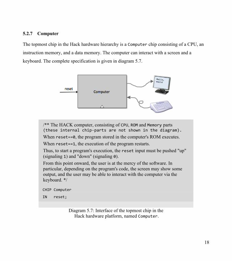
5.2.7 Computer
The topmost chip in the Hack hardware hierarchy is a Computer chip consisting of a CPU, an
instruction memory, and a data memory. The computer can interact with a screen and a
keyboard. The complete specification is given in diagram 5.7.
/** The HACK computer, consisting of CPU, ROM and Memory parts (theseinternalchip-partsarenotshowninthediagram). When reset==0, the program stored in the computer's ROM executes. When reset==1, the execution of the program restarts. Thus, to start a program's execution, the reset input must be pushed "up" (signaling 1) and "down" (signaling 0). From this point onward, the user is at the mercy of the software. In particular, depending on the program's code, the screen may show some output, and the user may be able to interact with the computer via the keyboard. */
CHIPComputer
INreset;
Diagram 5.7: Interface of the topmost chip in the Hack hardware platform, named Computer.

19
5.3 Implementation
This section outlines how a hardware platform can be built to realize the Hack computer
specification described in the previous section. As usual, we don’t give exact building
instructions. Rather, we expect readers to discover and complete the implementation details on
their own. All the chips described below can be built in HDL and simulated on a personal
computer, using the hardware simulator supplied with the book. As usual, technical details are
given in the final Project section of this chapter.
5.3.1 The Central Processing Unit
When we set out to implement the Hack CPU, our objective is to come up with a logic gate
architecture capable of (i) executing a given Hack instruction, and (ii) determining which
instruction should be fetched and executed next. In order to do so, the proposed CPU
implementation includes an ALU chip capable of computing arithmetic/logical functions, a set of
registers, a program counter, and some additional gates designed to help decode, execute, and
fetch instructions. Since all these building blocks were already built in previous chapters, the
key question that we face now is how to arrange and connect them in a way that effects the
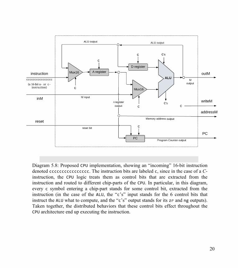
desired CPU operation. One possible configuration is illustrated in diagram 5.8.
The architecture shown in diagram 5.8 is used to perform three classical CPU tasks: decoding
the current instruction, executing the current instruction, and deciding which instruction to fetch
and execute next. We now turn to describe these three tasks.
20
Diagram 5.8: Proposed CPU implementation, showing an “incoming” 16-bit instruction denoted cccccccccccccccc. The instruction bits are labeled c, since in the case of a C-instruction, the CPU logic treats them as control bits that are extracted from the instruction and routed to different chip-parts of the CPU. In particular, in this diagram, every c symbol entering a chip-part stands for some control bit, extracted from the instruction (in the case of the ALU, the “c’s” input stands for the 6 control bits that instruct the ALU what to compute, and the “c’s” output stands for its zr and ng outputs). Taken together, the distributed behaviors that these control bits effect throughout the CPU architecture end up executing the instruction.

21
Instruction decoding
The 16-bit value of the CPU’s instruction input represents either an A-instruction or a C-
instruction. In order to figure out the semantics of this instruction, we can parse, or unpack it,
into the following fields: “ixxaccccccdddjjj”. The i-bit (also known as opcode) codes the
instruction type, which is either 0 for an A-instruction or 1 for a C-instruction. In case of an A-
instruction, the entire instruction represent the 16-bit value of the constant that should be loaded
into the A register. In case of a C-instruction, the a- and c-bits code the comp part of the
instruction, while the d- and j-bits code the dest and jump parts of the instruction, respectively
(the x-bits are not used, and can be ignored).
Instruction Execution
The decoded fields of the instruction (i-, a-, c-, d-, and j-bits) are routed simultaneously to
various parts of the CPU architecture, where they cause different chip-parts to do what they are
supposed to do in order to execute either the A- or the C-instruction, as mandated by the Hack
machine language specification. In the case of a C-instruction, the single a-bit determines
whether the ALU will operate on the A register input or on the M input, and the six c-bits
determine which function the ALU will compute. The three d-bits are used to determine which
registers should “accept” the ALU resulting output, and the three j-bits are used to for branching
control, as we now turn to describe.
Instruction Fetching
As a side effect of executing the current instruction, the CPU must determine, and emit, the
address of the instruction that should be fetched and executed next. The key element in this sub-
task is the Program Counter—a CPU chip-part whose role is to always store the address of the
next instruction. Later in the chapter we’ll describe how we connect the pc output of the CPU
into the address input of the instruction memory; this connection causes the instruction
22
memory to always emit the instruction that ought to be fetched and executed next. This output
is connected to the instruction input of the CPU, closing the fetch-execute cycle.
According to the Hack computer specification, the current program is stored in the
instruction memory, starting at address 0. Hence, if we wish to start (or restart) a program’s
execution, we should reset the Program Counter to 0. That’s why in diagram 5.8 the reset
input of the CPU is fed directly into the reset input of the PC chip. If we’ll assert this bit, we’ll
effect PC=0, causing the computer to fetch and execute the first instruction in the program. What
should we do next? Normally, we’d like to execute the next instruction in the program.
Therefore, the default operation of the Program Counter is PC++.
But what if the instruction dictates to effect a “jump n” operation, where n is the address
of an instruction located anywhere in the program? According to the Hack language
specification, a “jump n” operation is realized using a sequence of two instructions. First, we
issue the A-instruction @n, which sets the A register to n; next, we issue a C-instruction that
includes a jump directive. According to the language specification, execution always branches
to the instruction that the A register points at. Thus, when implementing the CPU, one of our
challenges is to come up with a logic gate architecture that realizes the following behavior: if
jump then PC = A else PC++. The value of the Boolean expression jump depends on the
instruction’s j-bits and on the ALU output.
How to implement this logic? The answer is hinted by diagram 5.8. Note that the output
of the A register feeds into the input of the PC register. Recall that the latter chip has a load-bit
that enables it to accept a new input value. Thus, if we’ll assert this load-bit, we’ll cause the
architecture to effect the operation PC=A rather than the default operation PC++. We should do
this only if we have to realize a jump. Now, the question of weather or not a jump should be
realized is answered by two signals: (i) the j-bits of the current instruction, specifying the jump

23
condition, and (ii) the ALU output-bits zr and ng, which can be used to determine if the specified
condition is satisfied, or not.
We’ll stop here, lest we rob readers the pleasure of discovering the missing details and
completing the CPU implementation on their own.
5.3.2 Memory
The Hack Memory chip is essentially an amalgamation of three lower-level chips: RAM16K,
Screen, and Keyboard. Yet this modularity is strictly implicit: users of the Memory chip, like
Hack programmers or programmers who write compilers that generate Hack code, see a single
address space, spanning from address 0 to address 24576 (0×0000 to 0×6000 in hexa).
The implementation of the Memory chip (as shown in diagram 5.6) should realize this
continuum effect. For example, if the address input of the Memory chip happens to be 16384,
the chip logic should end up accessing address 0 in the Screen chip, and so on. This can be
done using similar techniques to those used in chapter 3 to integrate small RAM units into
larger ones.
5.3.3 Computer
We have reached the end of our hardware journey. The topmost Computer chip can be realized
using three previously built chip-parts: a CPU, a data Memory, and an instruction memory named
ROM32K. Diagram 5.9 gives the details.

24
Diagram 5.9: Proposed implementation of the platform’s topmost chip, Computer.
5.4 Project
Objective: Build the Hack computer platform, culminating in the topmost Computer chip.
Resources: The only resources that you need for completing this project are the hardware
simulator supplied with the book and the test materials described here. The computer platform
should be written in HDL and tested using the hardware simulator.
Contract: Build a hardware platform capable of executing programs written in the Hack
machine language specified in chapter 4. Demonstrate the platform’s operations by having your
Computer chip run the three programs described below.
Test Programs: A natural way to test the overall Computer chip implementation is to have it
execute some sample programs written in the Hack machine language. In order to run such a

25
test, one can write a test script that loads the Computer chip into the hardware simulator, loads a
program from an external text file into its ROM chip, and then runs the clock enough cycles to
execute the program. We supply the following test programs (as well as all the relevant test
scripts and compare files):
• Add.hack: Adds the two constants 2 and 3 and writes the result in RAM[0].
• Max.hack: Computes the maximum of RAM[0] and RAM[1] and writes the result in RAM[2].
• Rect.hack: Draws on the screen a rectangle of RAM[0] rows of 16 pixels each.
Before testing your Computer chip on any one of the above programs, read the test script
associated with the program and be sure to understand the instructions given to the simulator. If
needed, consult Appendix B.
Steps: Implement the hardware platform in the following order:
Memory: Composed from three chips: RAM16K, Screen, and Keyboard. The Screen and the
Keyboard are available as built-in chips and there is no need to build them. Although the
RAM16K chip was built in project 3, we recommend using its built-in version, as it provides a
debugging-friendly GUI.
CPU: The central processing unit can be built according to the proposed implementation given
in figure 5.8, using the ALU and Register chips built in chapters 2 and 3, respectively. We
recommend using the built-in versions of these chips, in particular ARegister and DRegister.
These chips have exactly the same functionality of the Register chip specified in chapter 3,
plus GUI side effects.
In the course of implementing the CPU, you may be tempted to specify and build some
internal chips of your own. Be advised that there is no need to do so; The Hack CPU can be
implemented elegantly and efficiently using only the chip-parts that appear in diagram 5.8, plus
some elementary logic gates built in project 1.

26
Instruction Memory: Use the built-in ROM32K chip.
Computer: Build the topmost Computer chip using the three chip-parts shown in diagram 5.9.
The Hardware Simulator: All the chips in this project (including the topmost Computer chip)
can be implemented and tested using the supplied hardware simulator. Figure 5.10 is a screen
shot of testing the Rect.hack program on a Computer chip implementation.
Diagram 5.10: Testing the Computer chip on the supplied hardware simulator. The Rect program draws a rectangle of RAM[0] rows of 16 pixels each, all black, at the top-left of the screen. Note that the program is error-free. Therefore, if it does not operate as expected, it means that the hardware platform on which it is running (Computer.hdl and/or, possibly, some of it’s chip-parts) is buggy.

27
5.5 Perspective
Following the general spirit of the book, the architecture of the Hack computer is rather
minimal. Typical computer platforms have more registers, more data types, more powerful
ALUs, and richer instruction sets. However, these differences are mainly quantitative. From a
qualitative standpoint, Hack is quite similar to most digital computers, as they all follow the
same conceptual paradigm: the von Neumann architecture.
In terms of function, computer systems can be classified into two categories: general-
purpose computers, designed to easily switch from executing one program to another, and
dedicated computers, usually embedded in other systems like cell phones, game consoles,
digital cameras, weapon systems, factory equipment, and so on. For any particular application, a
single program is burned into the dedicated computer’s ROM, and is the only one that can be
executed (in game consoles, for example, the game software resides in an external cartridge that
is simply a replaceable ROM module encased in some fancy package). Aside from this
difference, general-purpose and dedicated computers share the same architectural ideas: stored
programs, fetch-decode-execute logic, CPU, registers, program counter, and so on.
Unlike Hack, most general-purpose computers use a single address space for storing
both data and instructions. In such architectures, the instruction address as well as the optional
data address specified by the instruction must be fed into the same destination: the single
address input of the shared address space. Clearly, this cannot be done at the same time. The
standard solution is to base the computer implementation on a two-cycle logic. During the fetch
cycle, the instruction address is fed to the address input of the memory, causing it to
immediately emit the current instruction, which is then stored in an instruction register. In the
subsequent execute cycle, the instruction is decoded, and the optional data address inferred from
it is fed to the memory’s address input, allowing the instruction to manipulate the selected
memory location. In contrast, the Hack architecture is unique in that it partitions the address

28
space into two separate parts, allowing a single-cycle fetch-execute logic. The price of this
simpler hardware design is that programs cannot be changed dynamically.
In terms of I/O, the Hack keyboard and screen are rather spartan. General-purpose
computers are typically connected to multiple I/O devices like printers, disks, network
connections, and so on. Also, typical screens are obviously much more powerful than the Hack
screen, featuring more pixels, many brightness levels in each pixel, and colors. Still, the basic
principle that each pixel is controlled by a memory-resident binary value is maintained: instead
of a single bit controlling the pixel’s black or white color, several bits are devoted to control the
level of brightness of each of the three primary colors that, together, produce the pixel’s
ultimate color. Likewise, the memory mapping of the Hack screen is simplistic. Instead of
mapping pixels directly into bits of memory, most modern computers allow the CPU to send
high-level graphic instructions to a graphics card that controls the screen. This way, the CPU is
relieved from the tedium of drawing figures like circles and polygons directly—the graphics
card takes care of this task using its own embedded chip-set.
Finally, it should be stressed that most of the effort and creativity in designing computer
hardware is invested in achieving better performance. Thus, hardware architecture courses and
textbooks typically evolve around such issues as implementing memory hierarchies (cache),
better access to I/O devices, pipelining, parallelism, instruction prefetching, and other
optimization techniques that were sidestepped in this chapter.
Historically, attempts to enhance the processor’s performance have led to two main
schools of hardware design. Advocates of the Complex Instruction Set Computing (CISC)
approach argue for achieving better performance by providing rich and elaborate instruction
sets. Conversely, the Reduced Instruction Set Computing (RISC) camp uses simpler instruction
sets in order to promote as fast a hardware implementation as possible. The Hack computer

29
does not enter this debate, featuring neither a strong instruction set nor special hardware
acceleration techniques.