Embed Size (px)
Citation preview

3DlInkjet-printed Origami Antennas for Multi-direction RF Harvesting
John Kimionis*, Apostolos Georgiadist, Michael Isakov+, Hang J. Qi+, and Manos M. Tentzeris* *School of Electrical and Computer Engineering, Georgia Institute of Technology, Atlanta, Georgia 30332-0250
Email: [email protected], [email protected] tCentre Tecnologic de Telecommunicacions de Catalunya, Castelldefels 08860, Spain
Email: [email protected]
* School of Mechanical Engineering, Georgia Institute of Technology, Atlanta, Georgia 30332-0250
Email: [email protected], [email protected]
Ahstract-A system design is presented for radio frequency (RF) energy harvesting on wireless sensor network (WSN) nodes, where all electronics reside inside a 3D structure and the antennas lie on the surfaces of it. Additive manufacturing techniques are used for the packaging and antenna fabrication: A 3D-printed cross-shaped structure is built that folds to a cuboid in an "origami" fashion and retains its shape at room temperature. Inkjet printing is used to directly fabricate antennas on the surfaces of the 3D-printed plastic, enabling a fully additive manufacturing of the structure. Multiple antennas on the cube's surfaces can be used for RF energy harvesting of signals arriving from totally orthogonal directions, with the use of an appropriate harvester. The system modules (cube, antenna, harvester) are described and characterized, offering a proof-of-concept for the combination of fabrication techniques to build systems for demanding RF applications.
Index Terms-RF energy harvesting, multiple antennas, additive manufacturing, inkjet printing, 3D printing.
I. INTRODUCTION
Low-cost and low-power connectivity is a necessity for
large-scale wireless sensor networks (WSNs). Power suffi
ciency is one of the most important scopes of designing WSN s,
and radio frequency (RF) energy harvesting gradually proves
that it is an enabling technology for demanding low-power
applications. The need for manually replacing batteries can be
eliminated by utilizing RF harvesting for autonomous sensor
operation, or for automatic battery recharging on-site [1], [2].
Towards that direction, a system design has been conceived
that will benefit WSN nodes in terms of harvesting and,
possibly, communication: All electronics of the WSN node
can reside inside 3D enclosures, such as cubes, that can
be easily deployed on a field. Currently, most WSN nodes
employ either wire monopole/dipole antennas, or planar patch
antennas. In both cases, the direction of maximum directivity
is limited to one dimension. Employing a 3D structure, such
as a cube, allows placing multiple antennas on it that face to
different directions. RF waves from totally orthogonal planes
can be exploited for harvesting and backscatter communi
cation, increasing the total system efficiency when multiple
sources are present. Such a system can also benefit in the
case of a single source that lies in an unknown direction:
two orthogonal antennas increase the probability of capturing
the source-emitted plane waves, compared to a single antenna
facing to a single direction that can only capture RF signals
Fig. 1. 3D cube with orthogonal-direction patch antennas on the sides and RF energy harvesting electronics inside.
from mUltipath reflections. Finally, the multiple antennas on
the sides of a compact cube can be tuned to different frequency
bands to benefit from ambient energy due to different sources:
FM radio, cellular networks, or Wi-Fi transmissions.
In this paper, the modules of the 3D energy harvesting
system are described and characterized, to demonstrate the us
ability of 3D-printed structures for wireless applications, such
as WSNs. Antennas are inkjet-printed on top of the 3D-printed
structures, thus showcasing the potential of combining additive
manufacturing technologies for complex RF applications.
II. 3D ANTENNAS
Due to the nature of the structure, where all electronics will
reside inside the cube, the antennas are designed as probe-fed
patches. A coaxial connector is used on the inside of the cube
that extends to a pin reaching the surface of the antenna to
excite it. The main advantage of using patch antennas is that
a ground plane on the backside of the cube's surfaces will
limit the electromagnetic coupling between the antenna and
the electronics circuit board.
The cube has been modeled in the ANSYS High Frequency
Structure Simulation (HFSS) software, and two patches for the
2.4 GHz band have been designed on two sides of the cube,
978-1-4799-8275-2/15/$31.00 ©2015 IEEE
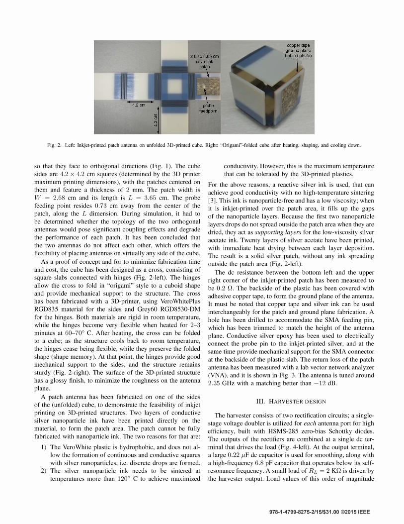
Fig. 2. Left: Inkjet-printed patch antenna on unfolded 3D-printed cube. Right: "Origami"-folded cube after heating, shaping, and cooling down.
so that they face to orthogonal directions (Fig. 1). The cube
sides are 4.2 x 4.2 cm squares (determined by the 3D printer
maximum printing dimensions), with the patches centered on
them and feature a thickness of 2 mm. The patch width is
W = 2.68 cm and its length is L = 3.65 cm. The probe
feeding point resides 0.73 cm away from the center of the
patch, along the L dimension. During simulation, it had to
be determined whether the topology of the two orthogonal
antennas would pose significant coupling effects and degrade
the performance of each patch. It has been concluded that
the two antennas do not affect each other, which offers the
flexibility of placing antennas on virtually any side of the cube.
As a proof of concept and for to minimize fabrication time
and cost, the cube has been designed as a cross, consisting of square slabs connected with hinges (Fig. 2-left). The hinges
allow the cross to fold in "origami" style to a cuboid shape
and provide mechanical support to the structure. The cross
has been fabricated with a 3D-printer, using VeroWhitePlus
RGD835 material for the sides and Grey60 RGD8530-DM
for the hinges. Both materials are rigid in room temperature,
while the hinges become very flexible when heated for 2-3 minutes at 60-70° C. After heating, the cross can be folded
to a cube; as the structure cools back to room temperature,
the hinges cease being flexible, while they preserve the folded
shape (shape memory). At that point, the hinges provide good
mechanical support to the sides, and the structure remains
sturdy (Fig. 2-right). The surface of the 3D-printed structure
has a glossy finish, to minimize the roughness on the antenna
plane.
A patch antenna has been fabricated on one of the sides
of the (unfolded) cube, to demonstrate the feasibility of inkjet
printing on 3D-printed structures. Two layers of conductive
silver nanoparticIe ink have been printed directly on the
material, to form the patch area. The patch cannot be fully
fabricated with nanoparticIe ink. The two reasons for that are:
1) The VeroWhite plastic is hydrophobic, and does not al
low the formation of continuous and conductive squares
with silver nanoparticles, i.e. discrete drops are formed.
2) The silver nanoparticIe ink needs to be sintered at
temperatures more than 120° C to achieve maximized
conductivity. However, this is the maximum temperature
that can be tolerated by the 3D-printed plastics.
For the above reasons, a reactive silver ink is used, that can
achieve good conductivity with no high-temperature sintering
[3]. This ink is nanoparticIe-free and has a low viscosity; when
it is inkjet-printed over the patch area, it fills up the gaps
of the nanoparticle layers. Because the first two nanoparticIe
layers drops do not spread outside the patch area when they are
dried, they act as supporting layers for the low-viscosity silver
acetate ink. Twenty layers of silver acetate have been printed,
with immediate heat drying between each layer deposition.
The result is a solid silver patch, without any ink spreading
outside the patch area (Fig. 2-left).
The dc resistance between the bottom left and the upper
right corner of the inkjet-printed patch has been measured to
be 0.2 Sl. The backside of the plastic has been covered with
adhesive copper tape, to form the ground plane of the antenna.
It must be noted that copper tape and silver ink can be used
interchangeably for the patch and ground plane fabrication. A
hole has been drilled to accommodate the SMA feeding pin,
which has been trimmed to match the height of the antenna
plane. Conductive silver epoxy has been used to electrically
connect the probe pin to the inkjet-printed silver, and at the
same time provide mechanical support for the SMA connector
at the backside of the plastic slab. The return loss of the patch
antenna has been measured with a lab vector network analyzer
(V NA), and it is shown in Fig. 3. The antenna is tuned around
2.35 GHz with a matching better than -12 dB.
III. HARVESTER DESIGN
The harvester consists of two rectification circuits; a single
stage voltage doubler is utilized for each antenna port for high
efficiency, built with HSMS-285 zero-bias Schottky diodes.
The outputs of the rectifiers are combined at a single dc ter
minal that drives the load (Fig. 4-left). At the output terminal,
a large 0.22 fLF dc capacitor is used for smoothing, along with
a high-frequency 6.8 pF capacitor that operates below its selfresonance frequency. A small load of RL = 2 KSl is driven by
the harvester output. Load values of this order of magnitude
978-1-4799-8275-2/15/$31.00 ©2015 IEEE
o
iii' :E. -5 '" '" .3 I: 5 Gi a: -10
_15L--�-�-�-�--�-�-�----.J
2 2.1 2.2 2.3 2.4 2.5 2.6 2.7 2.8 Frequency (GHz)
Fig. 3. Patch antenna measured return loss.
Fig. 4. Left: 2-port harvester schematic. Right: Harvester fabricated prototype.
Fig. 5. Measured harvester port 1 and port 2 return loss and coupling.
can be found in devices such as low-power microcontrollers
that can be used for WSN node implementations.
The 2-port harvester has been designed and simulated with
the Agilent Advanced Design System (ADS) software, using
large signal S-parameters (LSSP) and harmonic balance (HB)
simulations. Non-linear models have been utilized for the
diodes, and passive components have been simulated with
models that include parasitics. The harvester has been imple
mented on a thin (20 mil) Rogers R04003C laminate with
Er = 3.55 and tan (j = 0.002, and can be seen in Fig. 4-right.
The harvester has been tuned with single stubs for low input
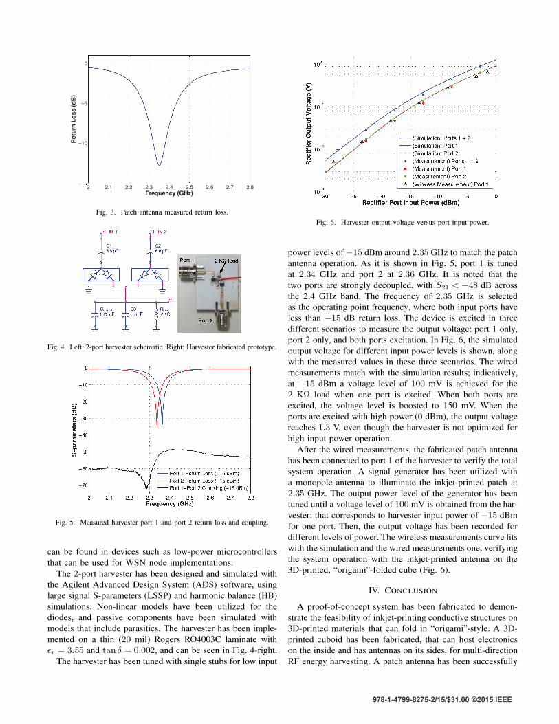
Fig. 6. Harvester output voltage versus port input power.
power levels of -15 dBm around 2.35 GHz to match the patch
antenna operation. As it is shown in Fig. 5, port 1 is tuned
at 2.34 GHz and port 2 at 2.36 GHz. It is noted that the
two ports are strongly decoupled, with S21 < -48 dB across
the 2.4 GHz band. The frequency of 2.35 GHz is selected
as the operating point frequency, where both input ports have
less than -15 dB return loss. The device is excited in three
different scenarios to measure the output voltage: port 1 only,
port 2 only, and both ports excitation. In Fig. 6, the simulated
output voltage for different input power levels is shown, along
with the measured values in these three scenarios. The wired
measurements match with the simulation results; indicatively,
at -15 dBm a voltage level of 100 mV is achieved for the
2 KO load when one port is excited. When both ports are
excited, the voltage level is boosted to 150 mY. When the
ports are excited with high power (0 dBm), the output voltage
reaches 1.3 V, even though the harvester is not optimized for
high input power operation .
After the wired measurements, the fabricated patch antenna
has been connected to port 1 of the harvester to verify the total
system operation. A signal generator has been utilized with
a monopole antenna to illuminate the inkjet-printed patch at
2.35 GHz. The output power level of the generator has been tuned until a voltage level of 100 mV is obtained from the har
vester; that corresponds to harvester input power of -15 dBm
for one port. Then, the output voltage has been recorded for
different levels of power. The wireless measurements curve fits
with the simulation and the wired measurements one, verifying
the system operation with the inkjet-printed antenna on the
3D-printed, "origami"-folded cube (Fig. 6).
IV. CONCLUSION
A proof-of-concept system has been fabricated to demon
strate the feasibility of inkjet-printing conductive structures on
3D-printed materials that can fold in "origami"-style. A 3D
printed cuboid has been fabricated, that can host electronics
on the inside and has antennas on its sides, for multi-direction
RF energy harvesting. A patch antenna has been successfully
978-1-4799-8275-2/15/$31.00 ©2015 IEEE

fabricated on the cube surface, using inkjet printing, and a full
RF harvesting system has been demonstrated. The proposed
structure is one of the first prototypes to demonstrate the
combination of additive manufacturing techniques such as
3D printing and inkjet printing, to enable the fabrication of
complex structures for rugged RF and packaging applications.
ACKNOWLEDGEMENT
This work was supported by the National Science
Foundation-EFRI, the Defense Threat Reduction Agancy,
Generalitat de Catalunya under grant 2014 SGR 1551, and
the Spanish Ministry of Economy and Competitiveness and
FEDER funds through the project TEC2012-39143. The au
thors would also like to acknowledge EU COST Action
IC1301 "Wireless Power Transmission for Sustainable Elec
tronics (WIPE)."
REFERENCES
[1] S. Kim, R. Vyas. 1. Bito. K. Niotaki, A. Collado. A. Georgiadis, and M. M. Tentzeris. "Ambient RF energy-harvesting technologies for selfsustainable standalone wireless sensor platforms," Proc. IEEE, vol. 102, no. 11, pp. 1649-1666, Nov. 2014.
[2] K. Gudan, S. Chemishkian, 1. 1. Hull, S. 1. Thomas, 1. Ensworth, and M. S. Reynolds, "A 2.4GHz ambient rf energy harvesting system with -20dBm minimum input power and NiMH battery storage," in IEEE Int. Con! on RFlD-Technology and Applications (RFlD-TA), Tampere, Finland, Sep. 2014, pp. 7-12.
[3] S. B. Walker and 1. A. Lewis, "Reactive silver inks for patterning highconductivity features at mild temperatures," fournal of the American Chemical Society, vol. 134, no. 3, pp. 1419-1421, 2012.
978-1-4799-8275-2/15/$31.00 ©2015 IEEE