Embed Size (px)
Citation preview
3D-Printed Frequency Selective Surfaces for
Microwave Absorbers
Rainer Kronberger, Patrick Soboll High Frequency Laboratory, TH Koeln University of Technology, Arts and Sciences
Betzdorfer Str. 2, D-50679 Koeln, Germany
Abstract - A flat periodic FSS (frequency selective surface) is
presented, which is fully fabricated by a 3D-printer and commercial 3D printing filaments which normally are used for printing metal like structures. The FSS absorber structure was
developed and optimized for 10 GHz, fabricated with the 3D printer, measured afterwards and compared with the simulations. Further simulations were made with the new
materials at higher frequencies and the results confirm that 3D printing technology works well and could be used to the best advantage for absorbers and other applications in the
frequency range below 100 GHz.
Index Terms — 3D-Printing, printed absorber, FSS.
1. Introduction
3D printing has become very popular within the last years.
In the same way, first investigations with 3D-printed devices
were made in the field of electromagnetics and latest
publications show that this new printing technology can also
be used to the best advantage for RF and microwave
engineering, e.g. for creating dielectric microwave and
antenna parts [1-3]. It is also reported about the typical
material properties of those thermoplastic filaments. In the
following a new application for such 3D printed devices is
presented, namely a printed frequency selective surface (FSS)
for electromagnetic wave absorption. In this paper the 3D
printing technology is used to create a flat and thin
metamaterial like FSS absorber in the X-Band.
2. Investigation of the Printing Filaments
Normally, 3D printer filaments are made of plastic, like
PLA (polylactic acid) or ABS and are available in all kind of
colors. From ColorFabb, (Netherlands, [4]), special printing
materials are offered, named CopperFill and BrassFill,
which were developed for printing metallic like parts and
which contain real metallic powder in the filaments. This fact
gave us the idea that the metallic powder inside may also
increase the electrical conductivity. Compared to
conventional printer filaments (more or less dielectrics with
moderate losses), this new material feature might enable the
printing of novel RF and microwave structures for a variety
of new applications (shieldings, antennas, etc.) where
conductivity is needed [2]. Before starting the design and
simulation process of the FSS structure, the exact electrical
material parameters of the different filaments had to be
determined. 2 mm thin material probes were printed and
filled into a WR-90 waveguide (22.86 mm x 10.16 mm),
then the scattering parameters of the probes were measured
at 10 GHz and afterwards evaluated [5]. Despite the fact that
there were no magnetic particles (e.g. carbonyl iron powder)
in the material, artificial and effective permeability with r >
1 appeared (see table I). With some measurements even an
effective r < 1 showed up. Such a behavior has been
observed with other composites as well [6, 7] and is
explained by the percolation phenomena in the microwave
regime. Isolated conductive particles in an insulating host
medium have a tendency to form clusters and eventually
connected chains which cause eddy currents and therefore
provide effective magnetic behavior with artificial effective
relative permeability. It must be said that the material
parameter measurements are critical. They were performed
several times with different probes, leading to different
results. The best fitting values for the simulation were
measured with probes at the same thickness as the realized
absorbers.
TABLE I
Measured Material Parameters (10 GHz)
Material Density
g/cm-3
r tan r tan
µ
BrassFill 2.4 8.15 0.015 1.25 0.2
CopperFill 3.0 8.3 0.08 1.35 0.025
3. Simulation and Printing Process
FSS absorber design is manifold and a variety of solutions
can be found in literature. As there are no comparable
publications and experiences with the above described
materials we started in a first attempt with a simple and well
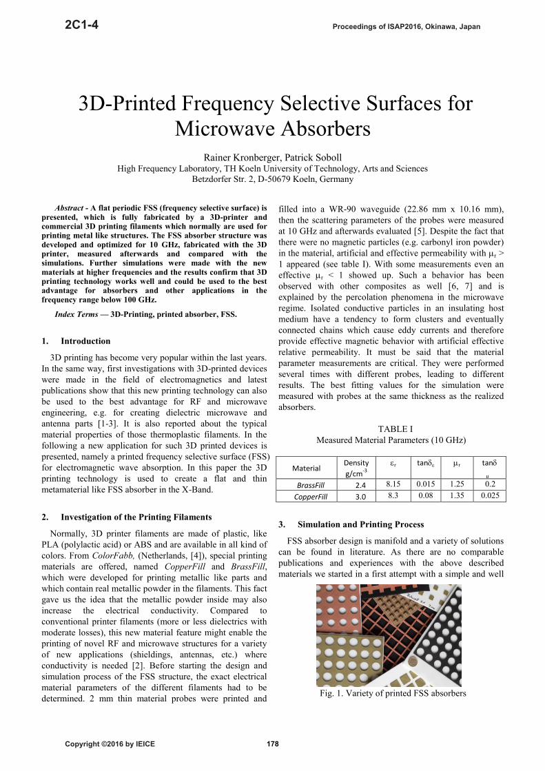
Fig. 1. Variety of printed FSS absorbers
Proceedings of ISAP2016, Okinawa, Japan
Copyright ©2016 by IEICE
2C1-4
178
known isolated quadratic patch design above PEC for 10
GHz, which has been used successfully with highly
conductive (PEC) or ink printed structures [e.g. 8 - 10]. All
simulations were performed with CST, using a unit cell and
Floquet boundaries. Simulations with BrassFill material
gave us a size of 20.3 mm for those squares, which were
printed directly on a high performance Rohacell71 foam
spacer with a height of 3 mm and low relative permittivity
close to one (r = 1.09, tan = 0.0038 @10 GHz) (refer to
Fig. 1). The printing process of the structure was done with
the 3D printer Ultimaker 2 [11], equipped with a 0.4 mm
printer nozzle. The specified printing accuracy is given with
approximately 0.1 mm, related to the height of the printed
device. This mainly results from the manual adjustment of
the base plate of the printer referred to the printing nozzle.
Printing accuracy could be confirmed by measurements.
However, the cooling process of the thermoplastic material
caused mechanical forces on the Rohacell [12] sheet and
finally resulted in unexpected dishing of the whole absorber.
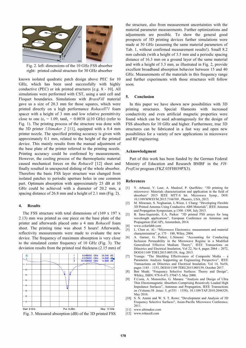
Therefore the basic FSS layer structure was changed from
isolated patches to periodic aperture holes in one common
part. Optimum absorption with approximately 25 dB at 10
GHz could be achieved with a diameter of 20.2 mm, a
spacing distance of 26.8 mm and a height of 2.1 mm (Fig. 2).
4. Results
The FSS structure with total dimensions of (169 x 197 x
2.13) mm was printed as one piece on the base plate of the
printer and afterwards placed onto a 4 mm Rohacell foam
sheet. The printing time was about 5 hours! Afterwards,
reflectivity measurements were made to evaluate the new
device. The frequency of maximum absorption is very close
to the simulated center frequency of 10 GHz (Fig. 3). The
deviation results from the printed real thickness (2.15 mm) of
the structure, also from measurement uncertainties with the
material parameter measurements. Further optimizations and
adjustments are possible. To show the general good
prospects of 3D printing devices further simulations were
made at 30 GHz (assuming the same material parameters of
Tab. 1, without confirmed measurement results!). Small 8.2
mm cuboids (with a height of 3.5 mm and a periodic spacing
distance of 16.3 mm on a ground layer of the same material
and with a height of 3.3 mm, as illustrated in Fig. 2, provide
excellent broadband absorption behavior between 15 and 40
GHz. Measurements of the materials in this frequency range
and further experiments with those structures will follow
soon.
5. Conclusion
In this paper we have shown new possibilities with 3D
printing structures. Special filaments with increased
conductivity and even artificial magnetic properties were
found which can be used advantageously for the design of
FSS absorbers for 10 GHz and higher. Furthermore, true 3D
structures can be fabricated in a fast way and open new
possibilities for a variety of new applications in microwave
and RF engineering.
Acknowledgment
Part of this work has been funded by the German Federal
Ministry of Education and Research BMBF in the FH-
ProfUnt program (FKZ 03FH039PX3).
References
[1] Y. Arbaoui, V. Laur, A. Maalouf, P. Queffelec: “3D printing for microwave: Materials characterization and application in the field of
absorbers” 2015 IEEE MTT-S Int. Microwave Symp., DOI:
10.1109/MWSYM.2015.7166769 , Phoenix, USA, 2015. [2] M. Mirazaee, S. Noghanian, L.Wiest, I. Chang: “Developing Flexible
3D Printed Antenna Using Conductive ABS Materials”, IEEE Antenna
and Propagation Symposium, p.1308–1309, July 2015. [3] B. Sanz-Izquierdo, E.A. Parker: “3D printed FSS arrays for long
wavelength applications”; European Conference on Antennas and
Propagation (EuCAP), Amsterdam, 2014.
[4] www.colorfabb.com
[5] L. Chen et. Al.: “Microwave Electronics: measurement and material
characterization”, p. 175 – 180, Wiley, 2004. [6] A. Garner, G. Parker, L.Simone: “Accounting for Conducting
Inclusion Permeability in the Microwave Regime in a Modified
Generalized Effective Medium Theory”, IEEE Transactions on Dilectrics and Electrical Insulation, Vol 22, No 4, pages 2064 – 2072,
DOI10/1109 TDEI.2015.005159, Aug. 2015.
[7] Youngs: “The Shielding Effectiveness of Composite Media – a Parametric Analysis Supporting an Engineering Perspective”. IEEE
Transactions on Dilectrics and Electrical Insulation, Vol 14, No54,
pages 1145 – 1153, DOI10/1109 TDEI.2015.005159, October 2017. [8] Ben Munk: “Frequency Selective Surfaces: Theory and Design”,
Whiley, ISBN: 978-0-471-37047-5, May 2000.
[9] F.Costa, A. Monorchio, G. Manara: “Analysis and Design of Ultra Thin Electromagnetic Absorbers Comprising Resistively Loaded High
Impedance Surfaces”, Antennas and Propagation, IEEE Transactions
on (Volume:58 ,Issue: 5, p1551 - 1558), 10.1109/TAP.2010.2044329, May 2010.
[10] S. N. Azemi and W. S. T. Rowe: "Development and Analysis of 3D
Frequency Selective Surfaces", Asian-Pacific Microwave Conference, 2011.
[11] www.ultimaker.com
[12] www.rohacell.com
Fig. 3. Measured absorption (dB) of the 3D printed FSS
Fig. 2. left: dimensions of the 10 GHz FSS absorber
right: printed cuboid structure for 30 GHz absorber
179


![[1967] Sewall Wright - Surfaces of Selective Value](https://img.pdfslide.us/doc/110x75/577c805c1a28abe054a8574c/1967-sewall-wright-surfaces-of-selective-value.jpg)