Embed Size (px)
Citation preview

3D PCB Design

3D PCB DESIGN
www.altium.com
3D PCB DESIGN
When it comes to designing circuit boards, you know that being able to properly visualize your spacing, sizing, and layout is crucial to
a successful finished product with minimal setbacks. While standard PCB design software has its place, 3D PCB software allows you
to get a detailed look at your routing, components, and overall layout BEFORE you send your design out for a physical prototype. As
3D environments become more advanced, they become essential tools to advance your PCB designs to the next step. Whether
prototyping or sending to manufacture a 3D design environment makes it easier for you to see what needs additional attention.
Join us as we discuss topics relating to 3D PCB Design including:
Move 3D Interference Checking to Electronic Design for a More Efficient Flow
Using 3D STEP Models to Reduce Design Respins
How 3D Modeling Has Changed Electronics Design Forever
The Value of a Built-in 3D Measurement Tool
Creating 3D Component Bodies in a Footprint Library
3D PCB Design: Why You Need It and How It Will Help You

3D PCB DESIGN
www.altium.com
MOVE 3D INTERFERENCE CHECKING TO ELECTRONIC DESIGN FOR A
MORE EFFICIENT FLOW
During a typical design process it can take multiple iterations before your PCB fits its enclosure, leading to delayed schedules and
missed deadlines. How can you ensure your PCB fits right the first time? With 3D interference checking.
Every electronic product consists of both mechanical and electrical assemblies. The two need to fit together — you don’t want
electronic components interfering with the mechanical enclosure. Typically, the completed electronic design moves to mechanical
designers for 3D interference checking. Any component interference problems are identified and then passed back to the electrical
designer for necessary changes.
During this process, it can take multiple iterations before the electronics properly fit within the enclosure. This iterative approach
delays product completion negatively affecting schedules and in some cases can even cause missed deadlines. So how can you
shorten this timetable and successfully release your products on time?
A NEW METHODOLOGY
What’s needed is a methodology that gives electrical designers the opportunity to verify interference before the design is handed off
to mechanical designers. Using that methodology can reduce iterations, save time, and improve the overall accuracy of your

3D PCB DESIGN
www.altium.com
schedule. Let’s look at how this methodology works.
A BETTER APPROACH WITH STEP
The best way to reduce (or eliminate) iterations is for the electrical designer to verify clearance before it’s handed off to the
mechanical team. STEP files can be imported for each component and then embedded as a component property. This STEP model
can either be obtained from the manufacturer or manually created within the electrical design tool. Either way, it has the accurate
physical dimensions of the component. Embedding dimensions moves toward the goal of interference checking taking place
completely within ECAD.
Imported 3D STEP Model Enclosure Fitted Over PCB Design
STEP files are not limited to components. The mechanical housing itself can be imported as a STEP file from the mechanical designer.
Once this data is obtained, you then import it into the ECAD tool and verify that the all of the components and connectors fit
securely within the housing and mounting holes are where they belong. Any discrepancies can be quickly adjusted in the ECAD tool,
eliminating the interference. Once verified, the final electrical assembly design moves to the mechanical team for any further testing.
This methodology significantly reduces the number of iterations, saving time and money — and keeping the product on schedule.
CHECKING INTERFERENCES IN ALTIUM DESIGNER
Altium Designer supports both import and export of STEP models and files, allowing inference checking within the electrical design.
The component clearance rule verifies that all 3D bodies and models within the design adhere to the constraints you have defined.
Learn more about how to easily implement PCB 3D interference checking in Altium Designer by downloading a free white paper.

3D PCB DESIGN
www.altium.com
USING 3D STEP MODELS TO REDUCE DESIGN RESPINS
Integrating mechanical design workflows into electrical design tools has become a necessary component of today’s successful PCB
design processes. But transferring inaccurate design data back and forth between the ECAD and MCAD worlds can not only cause
frustrations felt by both design teams but can also drastically increase the number of design spins required to fit a PCB into its final
assembly. Regardless of the electrical design tool’s 3D capabilities, accurate component 3D modeling information is crucial to the
success of this process.
WHY 3D STEP MODELS?
Integrating mechanical design workflows into electrical design tools has become a necessary component of today’s successful PCB
design processes. But transferring inaccurate design data back and forth between the ECAD and MCAD worlds can not only cause
frustrations felt by both design teams but can also drastically increase the number of design spins required to fit a PCB into its final
assembly. Regardless of the electrical design tool’s 3D capabilities, accurate component 3D modeling information is crucial to the
success of this process.
WHAT IS THE ISSUE HERE?
MCAD tools traditionally supply all mechanical data, but some still rely on antiquated methods like DXF or IDF files to exchange that
data. While IDF can be useful for creating simple extrusions of component bodies many details are missed because of the limitations
of the IDF file. STEP model integration provides a significantly higher level of 3-dimensional data that can not only be passed over to
the MCAD world but can also be used directly in your ECAD tool.
Integration methods for STEP models can differ between toolsets. It is important that the model can be easily imported into the
footprint while also having the ability to be visually manipulated in the 3D environment. Having to switch between the native PCB tool
and a different 3D viewing environment can add yet another hurdle to this process.

3D PCB DESIGN
www.altium.com
Step Model in 3D Environment
SOLUTION
Adding and manipulating 3D models in a native 3D design environment like Altium Designer makes the unification of the ECAD and
MCAD worlds as efficient as possible. Download a free whitepaper about Embedding a 3D STEP Model in a Footprint White Paper to
find out how to reduce the number of required design spins while ensuring that your board fits right the first time.

3D PCB DESIGN
www.altium.com
HOW 3D MODELING HAS CHANGED ELECTRONICS DESIGN FOREVER
Designing electronics in the late 1990s or early 2000s was a very different experience than it is today. Older PCB designs often
weren’t limited regarding real estate. They also often didn’t have as many mechanical constraints as modern designs do. While it’s
true that electronic components are much smaller today than they were 15 to 20 years ago, the mechanical envelopes that they
must fit into have gotten smaller as well.
Today, it’s essential to investigate thoroughly both the mechanical aspects of a PCB and with the system that it is integrated. You can
no longer do one without the other. How has 3D modeling helped designers to investigate the mechanical aspects of a PCB design?
3D MODELING THE ALTIUM WAY
Altium was the first to introduce 3D technology to PCB design software, by making 3D integration available within the Altium
Designer Unified development platform. And the rest, as they say, is history. Altium Designer is now capable of importing and
exporting mechanical CAD files such as STEP. We’ve also taken strides to create direct interaction between Altium Designer and
SOLIDWORKS®, allowing for real Electrical and Mechanical interaction using either Parasolid models or SOLIDWORKS® part models.
Here are just a few of the ways our 3D technology has changed electronics design forever:

3D PCB DESIGN
www.altium.com
Rigid-Flex Designs
Altium Designer supports Rigid Flex design and allows you to model the complete Rigid Flex assembly in 3D, to ensure mechanical
compliance. It is also possible to export a 3D model of your Rigid Flex in its final orientation.
Rigid-Flex Modeling in Altium Designer in 3D
Creating Board Shapes from 3D Models
An electrical engineer can now import a mechanical STEP model into an Altium Designer PCB. The model would detail the required
PCB board shape and scale created by a mechanical engineer in a mechanical CAD package, including board cutouts, fillets, and
mounting holes. Once the electrical engineer has this, they can create the PCB board shape directly from the 3D model, ensuring
compliance with all mechanical requirements.

3D PCB DESIGN
www.altium.com
Rigid-Flex Modeling in Altium Designer in 3D
Modeling PCB Footprints in 3D
3D models can be attached directly to a PCB footprint and positioned as required on a footprint within a PCB library. This linking is
probably the most important step in ensuring a clean working design. When the footprint is placed onto a PCB layout, it can be
displayed in 3D and used for 3D DRC interference checking.
Altium Designer can create a 3D step model of a PCB footprint on the fly as information is entered into the appropriate fields in our
IPC-Compliant footprint wizard. The resulting footprint can then either be embedded into the PCB footprint, or saved to an external
PCB library.
THE NEW PCB DESIGN WORKFLOW
As we’ve seen, there are some great 3D enhancements in Altium Designer that can help you create high-quality products faster and
cheaper. These 3D enhancements have also had a dramatic impact on our day-to-day PCB design software workflow when
mechanical enclosures need to be accounted for. Explore all of the 3D enhancements in Altium Designer that have changed PCB
electronics design forever by downloading a free white paper today.
3D PCB DESIGN
www.altium.com
THE VALUE OF A BUILT-IN 3D MEASUREMENT TOOL
The built-in 3D measurement features in Altium Designer has advantages that go above and beyond your average design tool. Read
on to discover the true value of integrated 3D measurement capabilities.
The Altium Designer PCB layout editor gives designers the ability to display their board in glorious 3D. With the help of Microsoft®
DirectX, the PCB editor allows the complete visualization of printed circuit boards, completely loaded with all of their components.
You can then view the loaded board, zoom in, rotate it, and thoroughly examine it in full, three-dimensional detail. You can view it
from any angle or position that you choose, or even use orthographic projection to examine the board closely.
The Native 3D™ PCB editor gives the designer not only a highly realistic view of what the fully assembled board will look like, but also
the ability to perform critical design tasks, such as 3D clearance checking, examining the location and presentation of text strings,
inspecting each individual 3D layer within a single layer mode, and even performing measurements directly within 3D. But what
makes the 3D measuring tool in Altium Designer different from those available in any other PCB design software?
3D MEASUREMENT TOOL CAPABILITIES THAT GO BEYOND THE NORM
While other PCB tools may include a tool to measure distance from one component body to another, Altium Designer 3D
measurement can perform three sets of measurements, including:
3D PCB DESIGN
www.altium.com
From the first object to the board
From the second object to the board
Between two objects.
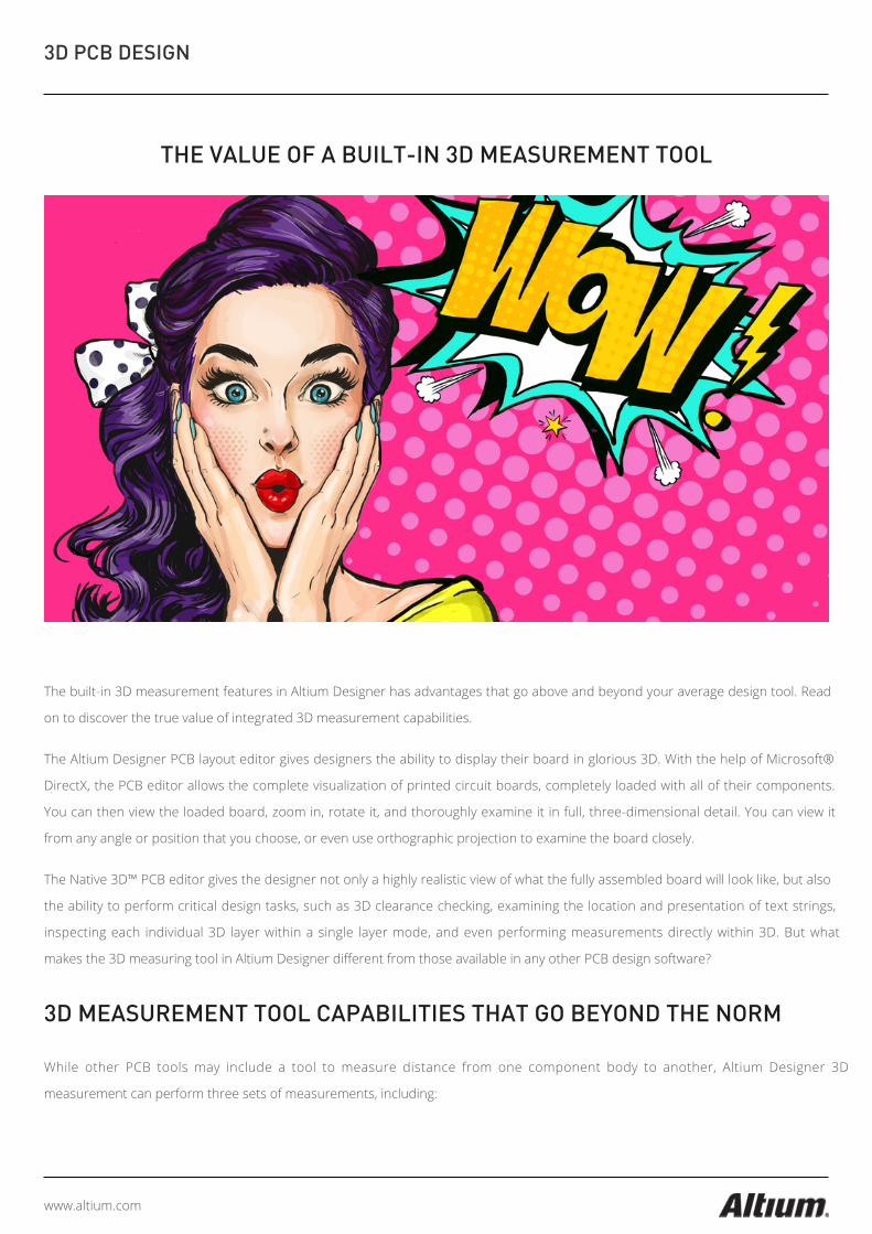
The 3D measurement function calculates the distance between the two closest points on the chosen objects or faces, displayed
them in yellow. All other measurements are shown in light blue as shown in the image below.
Object-to-Board Edge Measurements, from the Underside of a Plug-in Module Down to the Main Board
INSTANTANEOUS ACCESS TO SPECIFIC MEASUREMENT DATA
With the Native 3D™ PCB Editor within Altium Designer, you not only get a realistic view of your board layout, but also immediate
access to the most critical dimensional aspects needed to conceptualize your design. From 3D clearance checking to individual layer
inspection, you can obtain all necessary measurements at the click of a mouse.
Want to see how intuitive the built-in 3D measurement tool in Altium Designer really is? Download our free whitepaper 3D
Measuring in Altium Designer today!

3D PCB DESIGN
www.altium.com
CREATING 3D COMPONENT BODIES IN A FOOTPRINT LIBRARY
In today’s PCB design process, you need to be able to integrate mechanical design workflows into an electrical design tool. Read on
to learn how to easily create 3D component bodies in a footprint library.
In today’s PCB design process, you need to be able to integrate mechanical design workflows into an electrical design tool.
Transferring inaccurate design data back and forth between the ECAD and MCAD worlds not only causes frustrations for both design
teams, but can also drastically increase the number of design spins required to fit the PCB into its final assembly. And regardless of
the electrical design tool’s actual 3D capabilities, if you don’t have accurate component 3D modeling information, you can’t accurately
analyze mechanical clearances.
DOES YOUR DESIGN TOOL SUPPORT 3D MODELING?
Different EDA environments offer different levels of support for 3D modeling. Some have none at all, so all mechanical information
needs to be supplied by an MCAD tool. Others use outdated methods like DXF or IDF to exchange information. Altium Designer
supports embedding STEP models to provide accurate modeling information that can not only be passed over to the MCAD world,
but can also be used directly in ECAD tools.
There may be situations when you either can’t or simply don’t want to use a STEP model. You may not have an internal MCAD
department. You might not own any 3D MCAD tools. Or maybe your organization doesn’t allow externally-sourced CAD data of any
sort, thus preventing you from downloading the models. Other security restrictions may prevent you from accessing the Internet
altogether.
Fortunately, Altium Designer provides you with methodologies to create mechanical details of your components directly inside the
tool. This is ideally done in the footprint library itself (.PcbLib), but can also be done right at the board level (.PcbDoc) for one-off
situations.

3D PCB DESIGN
www.altium.com
3D View of a Component Model Shown in Altium Designer
HOW TO CREATE YOUR OWN 3D COMPONENT BODIES
Altium Designer provides three basic 3D shape types for creating mechanical models: Extruded, Cylinder, and Sphere. Each of these
can be used alone or in combination with one another. The Cylinder and Sphere types are self-explanatory.
Using these simple shapes, a large variety of surface mount and through-hole components can be created, ranging from the simple
to the surprisingly complex. Learn how to create your own 3D component bodies in Altium Designer by downloading a free white
paper.

3D PCB DESIGN
www.altium.com
3D PCB DESIGN: WHY YOU NEED IT AND HOW IT WILL HELP YOU
The other day I watched as a young father was entertaining his one-year old son on his shoulders. Securely held by his dad, the boy
would constantly move from side trying to get different views of his father. In an overload of cuteness, he would first look at his dad
over the left side of his face, then play with his hair, move over to the right side, then go back to where he started from.
I thoroughly enjoyed watching this precious moment, but it also brought to mind an important point. The child wanted every
possible different view of his father that he could get, and so he constantly changed his perspective. As PCB designers, we also want
to see every possible view of our designs. In the past, that perspective was constrained to working in a 2D CAD environment.
However, now that 3D design environments are becoming more accessible, we should use these tools to help advance our designs.
3D PCB DESIGN
www.altium.com
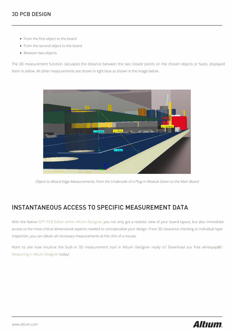
A 3D view of a PCB design has many benefits for the designer.
OLD SCHOOL DESIGN IN 2D AND BENEFITS OF 3D
When I first started out as a PCB designer I worked for a company that made display devices. This was still “back-in-the-day” when we
were using UNIX based CAD systems that only provided a 2D working environment. One of my first designs was sent over to the
mechanical CAD group where they rendered it in 3D for me. Even though it was only represented by primitive block shapes, I was still
amazed at how my design looked in 3D. It was the first time that I had ever seen one of my designs like this and the memory of that
moment has stayed with me. Working in a 3D environment can offer a lot of benefits to the PCB designer, here are a few of them.
3D Component Footprints: One of the first things that I noticed in looking at that design in 3D was that I had a large electrolytic
capacitor sticking up through the case of the device. This should have been caught by my DRC’s, but for some reason, it wasn’t.
Therefore it was a real surprise to me to see it waving out the back end of the device like the tail of a dog. In today’s CAD systems,
setting up your DRC’s for catching these types of errors is a standard feature. Now with the ability to work in 3D, you will have real-
time feedback for exactly how the heights of your components will look like.
Visualizing Layer Structures: PCB designers can benefit from being able to see exactly how a circuit board layer structure looks in 3D.
The designer can tilt, rotate, pan and zoom the image to see what a via stack will look like and exactly how it is interacting with the
other objects around it.
Full 3D Editing Capabilities: Viewing our designs in 3D is just the beginning since the layout can also be edited in the 3D mode. The
PCB designer is able to interactively ascend or descend through the circuit board stack-up in order move parts, push traces, or route
onto another layer.
MCAD/ECAD Collaboration: A 3D CAD system will also give you the ability to add a mechanical object to the design, such as the
device case. With this functionality, you will be able to view the 3D components in relation to the case, or other mechanical objects,

3D PCB DESIGN
www.altium.com
and run 3D clearance checks on these elements.
Flex Circuits: Another benefit to working in 3D is in designing flex circuits. With a full 3D environment you will now have the ability to
view the finished flex circuit folded up as it will be when assembled. Imagine that; you no longer have to guess how your flex design
will look when it is in use as you can use your 3D CAD system to give you an exact representation. This allows you to see assembly
and clearance problems that may arise with the design in its final folded configuration before going to the manufacturer. By finding
the problems first in your 3D CAD system, you will reduce the need for additional board spins to work out mechanical issues and
ultimately save money.
Working in a 3D environment will help PCB designers leverage the full potential of their design tools.
3D DESIGN: THE NEW STANDARD FOR TODAY’S DESIGN REQUIREMENTS
Traditionally, PCB designers have been constrained to working within a 2D environment. Although this standard has worked for
many years, today, PCB design is evolving quickly. Emerging technologies, such as wearable devices and the IoT, are moving the
design industry towards the need to work within 3D. With the competitive need to get the design to market first, PCB designs can no
longer afford the luxury of multiple board spins to work out manufacturing difficulties. Mechanical clearances, flex assembly details,
and component spacing problems can all be preemptively resolved before going to manufacturing by designing the board within a
3D environment.
Just like that little boy explored every possible perspective in order to get a better view of his dad, we also have the ability with 3D to
explore every perspective of our designs. The potential for a whole new way of designing circuit boards is right here in front of us, we
just have to dive in. Using 3D PCB design software, like Altium Designer, is an excellent way to get started.
Want the full picture of how 3D can help your designs? Then talk to our 3D design environment experts at Altium.
3D PCB DESIGN
www.altium.com
ADDITIONAL RESOURCES
Thank you for reading our guide on 3D PCB Design. To read more Altium resources, visit the Altium resource center here or join the
discussion at the bottom of each original blog post:
Move 3D Interference Checking to Electronic Design for a More Efficient Flow
Using 3D STEP Models to Reduce Design Respins
How 3D Modeling Has Changed Electronics Design Forever
The Value of a Built-in 3D Measurement Tool<
Creating 3D Component Bodies in a Footprint Library
3D PCB Design: Why You Need It and How It Will Help You