Embed Size (px)
Citation preview

MCP39113.3V Two-Channel Analog Front End
Features
• Two Synchronous Sampling 16/24-bit Resolution Delta-Sigma A/D Converters
• 94.5 dB SINAD, -106.5 dBc Total Harmonic Distortion (THD) (up to 35th harmonic), 111 dB SFDR for Each Channel
• 2.7V – 3.6V AVDD, DVDD
• Programmable Data Rate up to 125 ksps
- 4 MHz Maximum Sampling Frequency
• Oversampling Ratio up to 4096
• Ultra Low Power Shutdown Mode with <2 µA
• -122 dB Crosstalk between the Two Channels
• Low Drift 1.2V Internal Voltage Reference: 7 ppm/°C
• Differential Voltage Reference Input Pins
• High Gain Programmable Gain Amplifier (PGA) on Each Channel (up to 32V/V)
• Phase Delay Compensation with 1 µs Time Resolution
• Separate Modulator Output Pins for Each Channel
• Separate Data Ready Pin for Easy Synchronization
• Individual 24-bit Digital Offset and Gain Error Correction for Each Channel
• High-Speed 20 MHz SPI Interface with Mode 0,0 and 1,1 Compatibility
• Continuous Read/Write Modes for Minimum Communication
• Low Power Consumption (8.9 mW at 3.3V, 5.6 mW at 3.3V in low-power mode, typical)
• Available in Small 20-lead QFN and SSOP Packages, Pin-to-pin Compatible with MCP3901
• Extended Temperature Range: -40°C to +125°C
Applications
• Energy Metering and Power Measurement
• Automotive
• Portable Instrumentation
• Medical and Power Monitoring
• Audio/Voice Recognition
Description
The MCP3911 is a 2.7V to 3.6V dual channel AnalogFront End (AFE) containing two synchronous samplingDelta-Sigma Analog-to-Digital Converters (ADC), twoPGAs, phase delay compensation block, low-driftinternal voltage reference, modulator output block,digital offset and gain errors calibration registers andhigh-speed 20 MHz SPI compatible serial interface.
The MCP3911 ADCs are fully configurable withfeatures such as: 16/24-bit resolution, OSR from 32 to4096, gain from 1x to 32x, independent shutdown andreset, dithering and auto-zeroing. The communicationis largely simplified with the one-byte-long commandsincluding various continuous read/write modes that canbe accessed by the Direct Memory Access (DMA) of anMCU with a separate data ready pin that can be directlyconnected to an Interrupt Request (IRQ) input of anMCU.
The MCP3911 is capable of interfacing a large varietyof voltage and current sensors including shunts,current transformers, Rogowski coils and Hall effectsensors.
Package Type
OSC1/CLKI
1
23
4
20
1918
17
16
1514
13
5
67
8
OSC2
SDIRESET
DVDDAVDD
CH0+
CH0-
CH1-
129
DGND
MDAT0
MDAT1
DR CH1+
AGND
SDO
1110
REFIN+/OUT
REFIN-
CS
SCK
SD
O
20-Lead
SSOP
20-Lead
4x4 QFN*
2
CH1-
CH1+
CH0+ SCK
CS
RE
FIN
+/O
UT
OSC2
RE
FIN
-
DG
ND
MD
AT
1
OSC1/CLKI
AV
DD
DV
DD
RE
SE
T
SD
I
CH0- EP
20
1
19 18 17
3
4
14
13
12
11
6 7 8 9
21
5
10
15
16
AGND
MD
AT
0
DR
* Includes Exposed Thermal Pad (EP); see Table 3-1.
2012-2013 Microchip Technology Inc. DS20002286C-page 1

MCP3911
Functional Block Diagram
CH0+
CH0-
CH1+
CH1-
DUAL ����ADC
ANALOG DIGITAL
SINC3+SINC1
-
+
PGA
-
+
PGA ����Modulator
AMCLK
DMCLK/DRCLK
PhaseShifter� PHASE <11:0>
DATA_CH0<23:0>
MOD<7:0>
REFIN/OUT
REFIN-
AVDD
AGND DGND
DVDD
MOD<3:0>
MOD<7:4>
PORAVDD
Monitoring
����Modulator
VREF+VREF-
VREFEXTVoltageReference
VREF+
-
PORDVDD
Monitoring
SDO
SDISCK
Xtal OscillatorMCLK OSC1
OSC2
DR
RESETDigital SPIInterface
ClockGeneration
ModulatorOutput Block MDAT1
MDAT0
DMCLK OSR<2:0>PRE<1:0>
MODOUT<1:0>
CS
+
OFFCAL_CH0<23:0>
GAINCAL_CH0<23:0>
X
+
OFFCAL_CH1<23:0>
GAINCAL_CH1<23:0>
X DATA_CH1<23:0>
SINC3+SINC1
DS20002286C-page 2 2012-2013 Microchip Technology Inc.
MCP3911
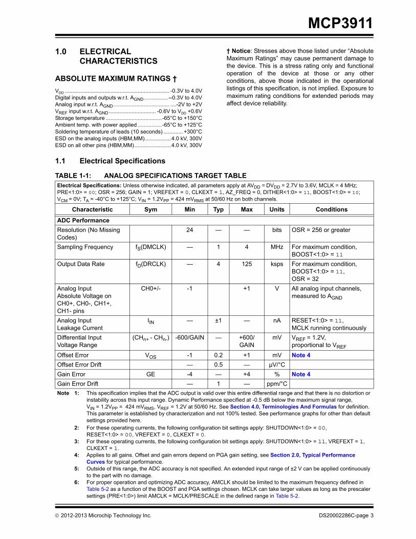
1.0 ELECTRICAL CHARACTERISTICS
ABSOLUTE MAXIMUM RATINGS †
VDD ..................................................................... -0.3V to 4.0VDigital inputs and outputs w.r.t. AGND................ --0.3V to 4.0VAnalog input w.r.t. AGND..................................... ....-2V to +2VVREF input w.r.t. AGND............................... -0.6V to VDD +0.6VStorage temperature .....................................-65°C to +150°CAmbient temp. with power applied ................-65°C to +125°CSoldering temperature of leads (10 seconds) ............. +300°CESD on the analog inputs (HBM,MM).................4.0 kV, 300VESD on all other pins (HBM,MM)........................4.0 kV, 300V
† Notice: Stresses above those listed under “AbsoluteMaximum Ratings” may cause permanent damage tothe device. This is a stress rating only and functionaloperation of the device at those or any otherconditions, above those indicated in the operationallistings of this specification, is not implied. Exposure tomaximum rating conditions for extended periods mayaffect device reliability.
1.1 Electrical Specifications
TABLE 1-1: ANALOG SPECIFICATIONS TARGET TABLEElectrical Specifications: Unless otherwise indicated, all parameters apply at AVDD = DVDD = 2.7V to 3.6V, MCLK = 4 MHz; PRE<1:0> = 00; OSR = 256; GAIN = 1; VREFEXT = 0, CLKEXT = 1, AZ_FREQ = 0, DITHER<1:0> = 11, BOOST<1:0> = 10; VCM = 0V; TA = -40°C to +125°C; VIN = 1.2VPP = 424 mVRMS at 50/60 Hz on both channels.
Characteristic Sym Min Typ Max Units Conditions
ADC Performance
Resolution (No Missing Codes)
24 — — bits OSR = 256 or greater
Sampling Frequency fS(DMCLK) — 1 4 MHz For maximum condition, BOOST<1:0> = 11
Output Data Rate fD(DRCLK) — 4 125 ksps For maximum condition, BOOST<1:0> = 11, OSR = 32
Analog Input Absolute Voltage on CH0+, CH0-, CH1+, CH1- pins
CH0+/- -1 +1 V All analog input channels, measured to AGND
Analog Input Leakage Current
IIN — ±1 — nA RESET<1:0> = 11, MCLK running continuously
Differential Input Voltage Range
(CHn+ - CHn-) -600/GAIN — +600/ GAIN
mV VREF = 1.2V, proportional to VREF
Offset Error VOS -1 0.2 +1 mV Note 4
Offset Error Drift — 0.5 — µV/°C
Gain Error GE -4 — +4 % Note 4
Gain Error Drift — 1 — ppm/°C
Note 1: This specification implies that the ADC output is valid over this entire differential range and that there is no distortion or instability across this input range. Dynamic Performance specified at -0.5 dB below the maximum signal range, VIN = 1.2VPP = 424 mVRMS, VREF = 1.2V at 50/60 Hz. See Section 4.0, Terminologies And Formulas for definition. This parameter is established by characterization and not 100% tested. See performance graphs for other than default settings provided here.
2: For these operating currents, the following configuration bit settings apply: SHUTDOWN<1:0> = 00, RESET<1:0> = 00, VREFEXT = 0, CLKEXT = 0.
3: For these operating currents, the following configuration bit settings apply: SHUTDOWN<1:0> = 11, VREFEXT = 1, CLKEXT = 1.
4: Applies to all gains. Offset and gain errors depend on PGA gain setting, see Section 2.0, Typical Performance Curves for typical performance.
5: Outside of this range, the ADC accuracy is not specified. An extended input range of ±2 V can be applied continuously to the part with no damage.
6: For proper operation and optimizing ADC accuracy, AMCLK should be limited to the maximum frequency defined in Table 5-2 as a function of the BOOST and PGA settings chosen. MCLK can take larger values as long as the prescaler settings (PRE<1:0>) limit AMCLK = MCLK/PRESCALE in the defined range in Table 5-2.
2012-2013 Microchip Technology Inc. DS20002286C-page 3

MCP3911
Integral Non-Linearity INL 5 ppm
Differential Input Impedance
ZIN 232 — — kΩ G = 1, proportional to 1/AMCLK
142 — — kΩ G = 2, proportional to 1/AMCLK
72 — — kΩ G = 4, proportional to 1/AMCLK
38 — — kΩ G = 8, proportional to 1/AMCLK
36 — — kΩ G = 16, proportional to 1/AMCLK
33 — — kΩ G = 32, proportional to 1/AMCLK
Signal-to-Noise and Distortion Ratio (Note 1)
SINAD 92 94.5 — dB
Total Harmonic Distortion (Note 1)
THD — -106.5 -103 dBc Includes the first 35 harmonics
Signal-to-Noise Ratio (Note 1)
SNR 92 95 — dB
Spurious Free Dynamic Range (Note 1)
SFDR — 111 — dBFS
Crosstalk (50, 60 Hz) CTALK — -122 — dB
AC Power Supply Rejection
AC PSRR — -73 — dB AVDD = DVDD = 3.3V+0.6VPP
, 50/60 Hz, 100/120 Hz
DC Power Supply Rejection
DC PSRR — -73 — dB AVDD = DVDD = 2.7V to 3.6V
DC Common Mode Rejection
DC CMRR — -105 — dB VCM from -1V to +1V
TABLE 1-1: ANALOG SPECIFICATIONS TARGET TABLE (CONTINUED)Electrical Specifications: Unless otherwise indicated, all parameters apply at AVDD = DVDD = 2.7V to 3.6V, MCLK = 4 MHz; PRE<1:0> = 00; OSR = 256; GAIN = 1; VREFEXT = 0, CLKEXT = 1, AZ_FREQ = 0, DITHER<1:0> = 11, BOOST<1:0> = 10; VCM = 0V; TA = -40°C to +125°C; VIN = 1.2VPP = 424 mVRMS at 50/60 Hz on both channels.
Characteristic Sym Min Typ Max Units Conditions
Note 1: This specification implies that the ADC output is valid over this entire differential range and that there is no distortion or instability across this input range. Dynamic Performance specified at -0.5 dB below the maximum signal range, VIN = 1.2VPP = 424 mVRMS, VREF = 1.2V at 50/60 Hz. See Section 4.0, Terminologies And Formulas for definition. This parameter is established by characterization and not 100% tested. See performance graphs for other than default settings provided here.
2: For these operating currents, the following configuration bit settings apply: SHUTDOWN<1:0> = 00, RESET<1:0> = 00, VREFEXT = 0, CLKEXT = 0.
3: For these operating currents, the following configuration bit settings apply: SHUTDOWN<1:0> = 11, VREFEXT = 1, CLKEXT = 1.
4: Applies to all gains. Offset and gain errors depend on PGA gain setting, see Section 2.0, Typical Performance Curves for typical performance.
5: Outside of this range, the ADC accuracy is not specified. An extended input range of ±2 V can be applied continuously to the part with no damage.
6: For proper operation and optimizing ADC accuracy, AMCLK should be limited to the maximum frequency defined in Table 5-2 as a function of the BOOST and PGA settings chosen. MCLK can take larger values as long as the prescaler settings (PRE<1:0>) limit AMCLK = MCLK/PRESCALE in the defined range in Table 5-2.
DS20002286C-page 4 2012-2013 Microchip Technology Inc.

MCP3911
Internal Voltage Reference
Tolerance VREF 1.176 1.2 1.224 V VREFEXT = 0, TA = +25°C only
Temperature Coefficient TCVREF — 7 — ppm/°C TA = -40°C to +125°C, VREFEXT = 0
Output Impedance ZOUTVREF — 2 — kΩ VREFEXT = 0
Internal Voltage Refer-ence Operating Current
AIDDVREF — 25 — µA VREFEXT = 0, SHUTDOWN<1:0> = 11
Voltage Reference Input
Input Capacitance — — 10 pF
Differential Input Voltage Range (VREF+ – VREF-)
VREF 1.1 — 1.3 V VREFEXT = 1
Absolute Voltage on REFIN+ pin
VREF+ VREF- + 1.1 — VREF-+ 1.3
V VREFEXT = 1
Absolute Voltage onREFIN- pin
VREF- -0.1 — +0.1 V REFIN- should be connected to AGND when VREFEXT = 0
Master Clock Input
Master Clock Input Frequency Range
fMCLK — 20 MHz CLKEXT = 1, Note 6
Crystal Oscillator Operating Frequency Range
fXTAL 1 — 20 MHz CLKEXT = 0, Note 6
Analog Master Clock AMCLK — — 16 MHz Note 6
Power Supply
Operating Voltage, Ana-log
AVDD 2.7 — 3.6 V
Operating Voltage, Digital DVDD 2.7 — 3.6 V
Operating Current, Analog (Note 2)
IDD,A — 1.5 2.3 mA BOOST<1:0> = 00
— 1.8 2.8 mA BOOST<1:0> = 01
— 2.5 3.5 mA BOOST<1:0> = 10
— 4.4 6.25 mA BOOST<1:0> = 11
TABLE 1-1: ANALOG SPECIFICATIONS TARGET TABLE (CONTINUED)Electrical Specifications: Unless otherwise indicated, all parameters apply at AVDD = DVDD = 2.7V to 3.6V, MCLK = 4 MHz; PRE<1:0> = 00; OSR = 256; GAIN = 1; VREFEXT = 0, CLKEXT = 1, AZ_FREQ = 0, DITHER<1:0> = 11, BOOST<1:0> = 10; VCM = 0V; TA = -40°C to +125°C; VIN = 1.2VPP = 424 mVRMS at 50/60 Hz on both channels.
Characteristic Sym Min Typ Max Units Conditions
Note 1: This specification implies that the ADC output is valid over this entire differential range and that there is no distortion or instability across this input range. Dynamic Performance specified at -0.5 dB below the maximum signal range, VIN = 1.2VPP = 424 mVRMS, VREF = 1.2V at 50/60 Hz. See Section 4.0, Terminologies And Formulas for definition. This parameter is established by characterization and not 100% tested. See performance graphs for other than default settings provided here.
2: For these operating currents, the following configuration bit settings apply: SHUTDOWN<1:0> = 00, RESET<1:0> = 00, VREFEXT = 0, CLKEXT = 0.
3: For these operating currents, the following configuration bit settings apply: SHUTDOWN<1:0> = 11, VREFEXT = 1, CLKEXT = 1.
4: Applies to all gains. Offset and gain errors depend on PGA gain setting, see Section 2.0, Typical Performance Curves for typical performance.
5: Outside of this range, the ADC accuracy is not specified. An extended input range of ±2 V can be applied continuously to the part with no damage.
6: For proper operation and optimizing ADC accuracy, AMCLK should be limited to the maximum frequency defined in Table 5-2 as a function of the BOOST and PGA settings chosen. MCLK can take larger values as long as the prescaler settings (PRE<1:0>) limit AMCLK = MCLK/PRESCALE in the defined range in Table 5-2.
2012-2013 Microchip Technology Inc. DS20002286C-page 5
MCP3911
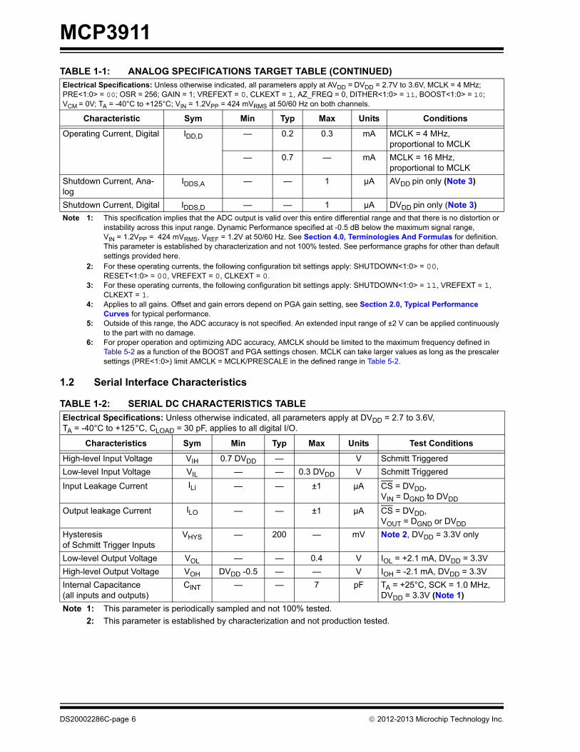
1.2 Serial Interface Characteristics
Operating Current, Digital IDD,D — 0.2 0.3 mA MCLK = 4 MHz, proportional to MCLK
— 0.7 — mA MCLK = 16 MHz, proportional to MCLK
Shutdown Current, Ana-log
IDDS,A — — 1 µA AVDD pin only (Note 3)
Shutdown Current, Digital IDDS,D — — 1 µA DVDD pin only (Note 3)
TABLE 1-2: SERIAL DC CHARACTERISTICS TABLE
Electrical Specifications: Unless otherwise indicated, all parameters apply at DVDD = 2.7 to 3.6V, TA = -40°C to +125°C, CLOAD = 30 pF, applies to all digital I/O.
Characteristics Sym Min Typ Max Units Test Conditions
High-level Input Voltage VIH 0.7 DVDD — V Schmitt Triggered
Low-level Input Voltage VIL — — 0.3 DVDD V Schmitt Triggered
Input Leakage Current ILI — — ±1 µA CS = DVDD, VIN = DGND to DVDD
Output leakage Current ILO — — ±1 µA CS = DVDD, VOUT = DGND or DVDD
Hysteresis of Schmitt Trigger Inputs
VHYS — 200 — mV Note 2, DVDD = 3.3V only
Low-level Output Voltage VOL — — 0.4 V IOL = +2.1 mA, DVDD = 3.3V
High-level Output Voltage VOH DVDD -0.5 — — V IOH = -2.1 mA, DVDD = 3.3V
Internal Capacitance(all inputs and outputs)
CINT — — 7 pF TA = +25°C, SCK = 1.0 MHz,DVDD = 3.3V (Note 1)
Note 1: This parameter is periodically sampled and not 100% tested.
2: This parameter is established by characterization and not production tested.
TABLE 1-1: ANALOG SPECIFICATIONS TARGET TABLE (CONTINUED)Electrical Specifications: Unless otherwise indicated, all parameters apply at AVDD = DVDD = 2.7V to 3.6V, MCLK = 4 MHz; PRE<1:0> = 00; OSR = 256; GAIN = 1; VREFEXT = 0, CLKEXT = 1, AZ_FREQ = 0, DITHER<1:0> = 11, BOOST<1:0> = 10; VCM = 0V; TA = -40°C to +125°C; VIN = 1.2VPP = 424 mVRMS at 50/60 Hz on both channels.
Characteristic Sym Min Typ Max Units Conditions
Note 1: This specification implies that the ADC output is valid over this entire differential range and that there is no distortion or instability across this input range. Dynamic Performance specified at -0.5 dB below the maximum signal range, VIN = 1.2VPP = 424 mVRMS, VREF = 1.2V at 50/60 Hz. See Section 4.0, Terminologies And Formulas for definition. This parameter is established by characterization and not 100% tested. See performance graphs for other than default settings provided here.
2: For these operating currents, the following configuration bit settings apply: SHUTDOWN<1:0> = 00, RESET<1:0> = 00, VREFEXT = 0, CLKEXT = 0.
3: For these operating currents, the following configuration bit settings apply: SHUTDOWN<1:0> = 11, VREFEXT = 1, CLKEXT = 1.
4: Applies to all gains. Offset and gain errors depend on PGA gain setting, see Section 2.0, Typical Performance Curves for typical performance.
5: Outside of this range, the ADC accuracy is not specified. An extended input range of ±2 V can be applied continuously to the part with no damage.
6: For proper operation and optimizing ADC accuracy, AMCLK should be limited to the maximum frequency defined in Table 5-2 as a function of the BOOST and PGA settings chosen. MCLK can take larger values as long as the prescaler settings (PRE<1:0>) limit AMCLK = MCLK/PRESCALE in the defined range in Table 5-2.
DS20002286C-page 6 2012-2013 Microchip Technology Inc.

MCP3911
TABLE 1-3: SERIAL AC CHARACTERISTICS TABLE
Electrical Specifications: Unless otherwise indicated, all parameters apply at DVDD = 2.7 to 3.6V, TA = -40°C to +125°C, GAIN = 1, CLOAD = 30 pF.
Characteristics Sym Min Typ Max Units Test Conditions
Serial Clock frequency fSCK — — 20 MHz
CS setup time tCSS 25 — — ns
CS hold time tCSH 50 — — ns
CS disable time tCSD 50 — — ns
Data setup time tSU 5 — — ns
Data hold time tHD 10 — — ns
Serial Clock high time tHI 20 — — ns
Serial Clock low time tLO 20 — — ns
Serial Clock delay time tCLD 50 — — ns
Serial Clock enable time tCLE 50 — — ns
Output valid from SCK low tDO — — 25 ns
Modulator output valid from AMCLK high
tDOMDAT — — 1/(2 x AMCLK) s
Output hold time tHO 0 — — ns (Note 1)
Output disable time tDIS — — 25 ns (Note 1)
Reset Pulse Width (RESET) tMCLR 100 — — ns
Data Transfer Time to DR (Data Ready)
tDODR — 25 ns (Note 2)
Modulator Mode Entry to Modulator Data Present
tMODSU — 100 ns
Data Ready Pulse Low Time tDRP 1/DMCLK — µs
Note 1: This parameter is periodically sampled and not 100% tested.
2: This parameter is established by characterization and not production tested.
TABLE 1-4: TEMPERATURE SPECIFICATIONS TABLE
Electrical Specifications: Unless otherwise indicated, all parameters apply at AVDD = 2.7 to 3.6V, DVDD = 2.7 to 3.6V.
Parameters Sym Min Typ Max Units Conditions
Temperature Ranges
Operating Temperature Range TA -40 — +125 °C Note 1
Storage Temperature Range TA -65 — +150 °C
Thermal Package Resistances
Thermal Resistance, 20L QFN θJA — 43 — °C/W
Thermal Resistance, 20L SSOP θJA — 87.3 — °C/W
Note 1: The internal junction temperature (TJ) must not exceed the absolute maximum specification of +150°C.
2012-2013 Microchip Technology Inc. DS20002286C-page 7

MCP3911
FIGURE 1-1: Serial Output Timing Diagram.
FIGURE 1-2: Serial Input Timing Diagram.
FIGURE 1-3: Data Ready Pulse/Sampling Timing Diagram.
tCSH
tDIS
tHI tLO
fSCK
CS
SCK
SDO MSB out LSB out
SDI
Mode 1,1
Mode 0,0
tHOtDO
DON’T CARE
CS
SCK
SDI LSB inMSB in
Mode 1,1
Mode 0,0
tCSS
tSU tHD
tCSD
tCSHtCLD
tCLE
SDOHI-Z
tHI tLO
fSCK
DR
SCK
tDRP
SDO
1/fD
tDODR
DS20002286C-page 8 2012-2013 Microchip Technology Inc.

MCP3911
H
FIGURE 1-4: Timing Diagrams (Continued).
CSVIH
Waveform for tDIS
HI-Z
90%
10%
tDISSDO
SCK
SDO
tDO
Timing Waveform for tDO
MDAT
OSC1/CLKI
Timing Waveform for MDAT0/1Modulator Output Function
tDOMDAT
2012-2013 Microchip Technology Inc. DS20002286C-page 9
MCP3911
NOTES:
DS20002286C-page 10 2012-2013 Microchip Technology Inc.

MCP3911
2.0 TYPICAL PERFORMANCE CURVES
Note: Unless otherwise indicated, AVDD = 3.3V, DVDD = 3.3V; TA = +25°C, MCLK = 4 MHz; PRESCALE = 1; OSR = 256; GAIN = 1; Dithering = Maximum; VIN = -0.5 dBFS at 60 Hz, VREFEXT = 0; CLKEXT = 1, AZ_FREQ = 0;BOOST = 1X.
FIGURE 2-1: Spectral Response.
FIGURE 2-2: Spectral Response.
FIGURE 2-3: THD Histogram.
FIGURE 2-4: Spectral Response.
FIGURE 2-5: Spectral Response.
FIGURE 2-6: SINAD Histogram.
Note: The graphs and tables provided following this note are a statistical summary based on a limited number ofsamples and are provided for informational purposes only. The performance characteristics listed hereinare not tested or guaranteed. In some graphs or tables, the data presented may be outside the specifiedoperating range (e.g., outside specified power supply range) and therefore outside the warranted range.
-200-180-160-140-120-100
-80-60-40-20
0
0 200 400 600 800 1000 1200 1400 1600 1800 2000
Am
plitu
de (d
B)
Frequency (Hz)
fIN = -0.5 dBFS @ 60 HzfD = 3.9 ksps16384 pt FFTOSR = 256Dithering = None
-200-180-160-140-120-100
-80-60-40-20
0
0 200 400 600 800 1000 1200 1400 1600 1800 2000
Am
plitu
de (d
B
Frequency (Hz)
fIN = -60 dBFS@ 60 HzfD = 3.9 ksps16384 pt FFTOSR = 256Dithering = None
-107.3 -107.1 -107.0 -106.8 -106.7 -106.5 -106.4 -106.2 -106.1 -105.9 -105.8
Freq
uenc
y of
Occ
urre
nce
Total Harmonic Distortion (-dBc)
-200-180-160-140-120-100
-80-60-40-20
0
0 200 400 600 800 1000 1200 1400 1600 1800 2000
Am
plitu
de (d
B)
Frequency (Hz)
fIN = -0.5 dBFS @ 60 HzfD = 3.9 ksps16384 pt FFTOSR = 256Dithering = Maximum
-200-180-160-140-120-100
-80-60-40-20
0
0 200 400 600 800 1000 1200 1400 1600 1800 2000
Am
plitu
de (d
B)
Frequency (Hz)
fIN = -60 dBFS @ 60 HzfD = 3.9 ksps16384 pt FFTOSR = 256Dithering = Maximum
94.2 94.3 94.5 94.6 94.8 94.9 95.1 95.2 95.4 95.5
Freq
uenc
y of
Occ
urre
nce
Signal-to-Noise and Distortion Ratio (dB)
2012-2013 Microchip Technology Inc. DS20002286C-page 11
MCP3911
Note: Unless otherwise indicated, AVDD = 3.3V, DVDD = 3.3V; TA = +25°C, MCLK = 4 MHz; PRESCALE = 1; OSR = 256; GAIN = 1; Dithering = Maximum; VIN = -0.5 dBFS at 60 Hz, VREFEXT = 0; CLKEXT = 1, AZ_FREQ = 0;BOOST = 1X.
FIGURE 2-7: Spurious Free Dynamic Range Histogram.
FIGURE 2-8: SNR Histogram.
FIGURE 2-9: Noise Histogram.
FIGURE 2-10: ENOB SINAD Histogram.
FIGURE 2-11: ENOB SNR Histogram.
FIGURE 2-12: THD vs. OSR.
104.5 106 107.5 109 110.5 112 113.5 115
Freq
uenc
y of
Occ
urre
nce
Spurious Free Dynamic Range (dBFS)
94.5 94.6 94.8 94.9 95.1 95.2 95.4 95.5 95.6 95.8 95.9
Freq
uenc
y of
Occ
urre
nce
Signal-to-Noise Ratio (dB)
0500
100015002000250030003500400045005000
Freq
uenc
y O
f Occ
urre
nce
Output Code (LSB)
Channel 1VIN = 0VTA = +25°C16384 Consecutive Readings
15.3 15.4 15.4 15.4 15.5 15.5 15.5 15.5 15.6 15.6
Freq
uenc
y of
Occ
urre
nce
Effective Number of Bits (SINAD)
15.4 15.4 15.5 15.5 15.5 15.5 15.6 15.6 15.6 15.6
Freq
uenc
y of
Occ
urre
nce
Effective Number of Bits (SNR)
-120-110-100-90-80-70-60-50-40-30-20-10
0
32 64 128 256 512 1024 2048 4096
Tota
l Har
mon
ic D
isto
rtio
n (d
Bc)
Oversampling Ratio (OSR)
Dithering = MaximumDithering = MediumDithering = MinimumDithering = None
DS20002286C-page 12 2012-2013 Microchip Technology Inc.
MCP3911
Note: Unless otherwise indicated, AVDD = 3.3V, DVDD = 3.3V; TA = +25°C, MCLK = 4 MHz; PRESCALE = 1; OSR = 256; GAIN = 1; Dithering = Maximum; VIN = -0.5 dBFS at 60 Hz, VREFEXT = 0; CLKEXT = 1, AZ_FREQ = 0;BOOST = 1X.
FIGURE 2-13: SINAD vs. OSR.L
FIGURE 2-14: SNR vs.OSR.
FIGURE 2-15: SFDR vs. OSR.
FIGURE 2-16: THD vs. MCLK.
FIGURE 2-17: SINAD vs. MCLK.
FIGURE 2-18: SNR vs. MCLK.
0102030405060708090
100110120
32 64 128 256 512 1024 2048 4096
Sign
al-to
-Noi
se a
nd D
isto
rtio
n R
atio
(dB
)
Oversampling Ratio (OSR)
Dithering = MaximumDithering = MediumDithering = MinimumDithering = None
0 102030405060708090
100110120
32 64 128 256 512 1024 2048 4096
Sign
al-to
-Noi
se R
atio
(dB
)
Oversampling Ratio (OSR)
Dithering = Maximum Dithering = Medium Dithering = Minimum Dithering = No e
0102030405060708090
100110120130140
32 64 128 256 512 1024 2048 4096
Spur
ious
Fre
e D
ynam
ic R
ange
(d
BFS
)
Oversampling Ratio (OSR)
Dithering = MaximumDithering = MediumDithering = MinimumDithering = None
-120-110-100-90-80-70-60-50-40-30-20-10
0
0 5 10 15 20 25 30
Tota
l Har
mon
ic D
isto
rtio
n (d
Bc)
MCLK Frequency (MHz)
Boost = 0.5x
Boost = 0.66x
Boost = 2x
Boost = 1x
0102030405060708090
100110120
0 5 10 15 20 25 30
Sign
al-to
-Noi
se a
nd D
isto
rtio
n R
atio
(dB
)
MCLK Frequency (MHz)
Boost = 0.5x
Boost = 0.66x
Boost = 2x
Boost = 1x
0102030405060708090
100110120
0 5 10 15 20 25 30
Sign
al-to
-Noi
se R
atio
(dB
)
MCLK Frequency (MHz)
Boost = 0.5xBoost = 0.66x
Boost = 2x
Boost = 1x
2012-2013 Microchip Technology Inc. DS20002286C-page 13

MCP3911
Note: Unless otherwise indicated, AVDD = 3.3V, DVDD = 3.3V; TA = +25°C, MCLK = 4 MHz; PRESCALE = 1; OSR = 256; GAIN = 1; Dithering = Maximum; VIN = -0.5 dBFS at 60 Hz, VREFEXT = 0; CLKEXT = 1, AZ_FREQ = 0;BOOST = 1X.
FIGURE 2-19: SFDR vs. MCLK.
FIGURE 2-20: SINAD vs. GAIN.
FIGURE 2-21: SINAD vs. GAIN (Dithering Off).
FIGURE 2-22: SINAD vs. GAIN vs. AZ Speed Chart.
FIGURE 2-23: THD vs. Input Signal Amplitude.
FIGURE 2-24: SINAD vs. Input Signal Amplitude.
0102030405060708090
100110120
0 5 10 15 20 25 30
Spur
ious
Fre
e D
ynam
ic R
ange
(d
BFS
)
Frequency (MHz)
Boost = 0.5x
Boost = 0.66x
Boost = 2x
Boost = 1x
0102030405060708090
100110120
1 2 4 8 16 32
Sign
al-to
-Noi
se a
nd D
isto
rtio
n R
atio
(dB
)
Gain (V/V)
OSR = 32OSR = 64OSR = 128OSR = 256OSR = 512OSR = 1024OSR = 2048OSR = 4096
0102030405060708090
100110120
1 2 4 8 16 32
Sign
al to
Noi
se a
nd D
isto
rtio
n R
atio
(dB
)
Gain (V/V)
OSR = 32OSR = 64OSR = 128OSR = 256OSR = 512OSR = 1024OSR = 2048OSR = 4096
70
75
80
85
90
95
100
1 2 4 8 16 32
Sign
al-to
-Noi
se a
nd D
isto
rtio
n R
atio
(dB
)
Gain (V/V)
Auto Zero Speed = Fast
Auto Zero Speed = Slow
-120-110-100-90-80-70-60-50-40-30-20-10
0
-6 -5 -4 -3 -2 -1 0 1 2 3
Tota
l Har
mon
ic D
isto
rtio
n (d
Bc)
Input Signal Amplitude (dBFS)
Channel 1Channel 0
0102030405060708090
100110120
-6 -5 -4 -3 -2 -1 0 1 2 3
Sign
al-to
-Noi
se a
nd D
isto
rtio
n R
atio
(dB
)
Input Signal Amplitude (dBFS)
Channel 1Channel 0
DS20002286C-page 14 2012-2013 Microchip Technology Inc.

MCP3911
Note: Unless otherwise indicated, AVDD = 3.3V, DVDD = 3.3V; TA = +25°C, MCLK = 4 MHz; PRESCALE = 1; OSR = 256; GAIN = 1; Dithering = Maximum; VIN = -0.5 dBFS at 60 Hz, VREFEXT = 0; CLKEXT = 1, AZ_FREQ = 0;BOOST = 1X.
FIGURE 2-25: SNR vs. Input Signal Amplitude.
FIGURE 2-26: SFDR vs. Input Signal Amplitude.
FIGURE 2-27: THD vs. Temperature.
FIGURE 2-28: SINAD vs. Temperature.
FIGURE 2-29: SNR vs. Temperature.
FIGURE 2-30: SFDR vs. Temperature.
0102030405060708090
100110120
-6 -5 -4 -3 -2 -1 0 1 2 3
Sign
al-to
-Noi
se R
atio
(dB
)
Input Signal Amplitude (dBFS)
Channel 1Channel 0
0102030405060708090
100110120
-6 -5 -4 -3 -2 -1 0 1 2 3
Spur
ious
Fre
e D
yanm
ic R
ange
(d
BFS
)
Input Signal Amplitude (dBFS)
Channel 0
Channel 1
-120-110-100-90-80-70-60-50-40-30-20-10
0
-50 -25 0 25 50 75 100 125 150
Tota
l Har
omin
c D
isto
rtio
n (d
Bc)
Temperature (°C)
G = 1G = 2G = 4G = 8G = 16G = 32
0102030405060708090
100
-50 -25 0 25 50 75 100 125 150
Sign
al-to
-Noi
se a
nd D
isto
rtio
n R
atio
(dB
)
Temperature (°C)
G = 1G = 2G = 4G = 8G = 16G = 32
0102030405060708090
100
-50 -25 0 25 50 75 100 125 150
Sign
al-to
-Noi
se R
atio
(dB
)
Temperature (°C)
G = 1G = 2G = 4G = 8G = 16G = 32
0102030405060708090
100110120
-50 -25 0 25 50 75 100 125 150
Spur
ious
Fre
e D
ynam
ic R
ange
(d
BFS
)
Temperature (°C)
G = 1G = 2G = 4G = 8G = 16G = 32
2012-2013 Microchip Technology Inc. DS20002286C-page 15
MCP3911
Note: Unless otherwise indicated, AVDD = 3.3V, DVDD = 3.3V; TA = +25°C, MCLK = 4 MHz; PRESCALE = 1; OSR = 256; GAIN = 1; Dithering = Maximum; VIN = -0.5 dBFS at 60 Hz, VREFEXT = 0; CLKEXT = 1, AZ_FREQ = 0;BOOST = 1X.
FIGURE 2-31: Channel 0 Offset vs. Temperature.
FIGURE 2-32: Channel 1 Offset vs. Temperature.
FIGURE 2-33: Channel-to-Channel Offset Match vs. Temperature.
FIGURE 2-34: Gain Error vs. Temperature.
FIGURE 2-35: Internal Voltage Reference vs. Temperature.
FIGURE 2-36: Internal Voltage Reference vs. Supply Voltage.
-100-50
050
100150200250300350400
-50 -25 0 25 50 75 100 125 150
Cha
nnel
1 O
ffset
(mV)
Temperature (°C)
G = 1G = 2G = 4G = 8G = 16G = 32
-100-50
050
100150200250300350400
-50 -25 0 25 50 75 100 125 150
Cha
nnel
0 O
ffset
(mV)
Temperature (°C)
G = 1G = 2G = 4G = 8G = 16G = 32
-120
-100
-80
-60
-40
-20
0
-50 -25 0 25 50 75 100 125 150
Offs
et E
rror
(mV)
Temperature (°C)
Channel 0
Channel 1
-5-4-3-2-1012345
-50 -25 0 25 50 75 100 125 150
Gai
n Er
ror (
%)
Temperature (°C)
G = 32 G = 16
G = 8
G = 4
G = 2
G = 1
1.1999
1.2000
1.2001
1.2002
1.2003
1.2004
1.2005
1.2006
1.2007
1.2008
-50 0 50 100 150
Inte
rnal
Vol
tage
Ref
eren
ce (V
)
Temperature (°C)
1.1997
1.1998
1.1999
1.2000
1.2001
1.2002
1.2003
2.5 2.6 2.7 2.8 2.9 3 3.1 3.2 3.3 3.4 3.5 3.6
Inte
rnal
Vol
tage
Ref
eren
ce (V
)
VDD (V)
DS20002286C-page 16 2012-2013 Microchip Technology Inc.

MCP3911
Note: Unless otherwise indicated, AVDD = 3.3V, DVDD = 3.3V; TA = +25°C, MCLK = 4 MHz; PRESCALE = 1; OSR = 256; GAIN = 1; Dithering = Maximum; VIN = -0.5 dBFS at 60 Hz, VREFEXT = 0; CLKEXT = 1, AZ_FREQ = 0;BOOST = 1X.
FIGURE 2-37: VREF Drift Data Histogram Chart.
FIGURE 2-38: Integral Non-Linearity (Dithering Maximum).
FIGURE 2-39: Integral Non-Linearity (Dithering Off).
FIGURE 2-40: Operating Current vs. MCLK, VDD = 3.3V.
FIGURE 2-41: Operating Current vs. MCLK, VDD = 2.7V.
0
2
4
6
8
10
12
14
0 3 6 9 12 15 18 21 24
Freq
uenc
y of
Occ
urre
nce
Internal Voltage Reference Drift (ppm/C)
-25-20-15-10
-505
10152025
-0.6 -0.3 0 0.3 0.6
Inte
gral
Non
-Lin
earit
y Er
ror
(ppm
)
Input Voltage (V)
Channel 0
Channel 1
-25-20-15-10
-505
10152025
-0.6 -0.3 0 0.3 0.6
Inte
gral
Non
-Lin
earit
y Er
ror
(ppm
)
Input Voltage (V)
Channel 0
Channel 1
00.5
11.5
22.5
33.5
44.5
0 2.5 5 7.5 10 12.5 15 17.5 20 22.5 25 27.5 30
I DD
(mA
)
MCLK Frequency (MHz)
AIDD, Boost = 2x
AIDD, Boost = 1x
AIDD, Boost = 0.6x
AIDD, Boost = 0.5x
DIDD, All Boost Settings
0
0.5
1
1.5
2
2.5
3
3.5
4
0 2.5 5 7.5 10 12.5 15 17.5 20 22.5 25 27.5 30
I DD
(mA
)
MCLK Frequency (MHz)
AIDD, Boost = 2x
AIDD, Boost = 1x
AIDD, Boost = 0.6x
AIDD, Boost = 0.5x
DIDD, All Boost Settings
2012-2013 Microchip Technology Inc. DS20002286C-page 17

MCP3911
NOTES:
DS20002286C-page 18 2012-2013 Microchip Technology Inc.

MCP3911
3.0 PIN DESCRIPTION
The descriptions of the pins are listed in Table 3-1.
3.1 Master Reset (RESET)
This pin is active-low and places the entire chip in aReset state when active.
When RESET = DGND, all registers are reset to theirdefault value, no communication can take place and noclock is distributed inside the part except in the inputstructure, if MCLK is applied (if idle, no clock isdistributed). This state is equivalent to a POR state.
Since the default state of the ADCs is on, the analogpower consumption when RESET = DGND isequivalent to RESET = VDD. Only the digital powerconsumption is largely reduced because this currentconsumption is essentially dynamic and is reduceddrastically when there is no clock running.
All the analog biases are enabled during a Reset sothat the part is fully operational just after a RESETrising edge, if the MCLK is applied during the risingedge. If not applied, there is a small time after RESETwhen the conversion may not be accurate,corresponding to the startup of the charge pump of theinput structure.
This input is Schmitt-triggered.
3.2 Digital VDD (DVDD)
DVDD is the power supply pin for the digital circuitrywithin the MCP3911. For specified operation, this pinrequires appropriate bypass capacitors and should bemaintained between 2.7V and 3.6V.
3.3 Analog VDD (AVDD)
AVDD is the power supply pin for the analog circuitrywithin the MCP3911. For specified operation, this pinrequires appropriate bypass capacitors and should bemaintained between 2.7V and 3.6V.
TABLE 3-1: PIN FUNCTION TABLE
Pin No. SSOP
Pin No. QFN
Symbol Function
1 18 RESET Master Reset Logic Input Pin
2 19 DVDD Digital Power Supply Pin
3 20 AVDD Analog Power Supply Pin
4 1 CH0+ Non-Inverting Analog Input Pin for Channel 0
5 2 CH0- Inverting Analog Input Pin for Channel 0
6 3 CH1- Inverting Analog Input Pin for Channel 1
7 4 CH1+ Non-Inverting Analog Input Pin for Channel 1
8 5 AGND Analog Ground Pin, Return Path for internal analog circuitry
9 6 REFIN+/OUT Non-Inverting Voltage Reference Input and Internal Reference Output Pin
10 7 REFIN- Inverting Voltage Reference Input Pin
11 8 DGND Digital Ground Pin, Return Path for internal digital circuitry
12 9 MDAT1 Modulator Data Output Pin for Channel 1
13 10 MDAT0 Modulator Data Output Pin for Channel 0
14 11 DR Data Ready Signal Output Pin
15 12 OSC1/CLKI Oscillator Crystal Connection Pin or External Clock Input Pin
16 13 OSC2 Oscillator Crystal Connection Pin
17 14 CS Serial Interface Chip Select Pin
18 15 SCK Serial Interface Clock Input Pin
19 16 SDO Serial Interface Data Input Pin
20 17 SDI Serial Interface Data Input Pin
— 21 EP Exposed Thermal Pad. Must be connected to AGND or left floating.
2012-2013 Microchip Technology Inc. DS20002286C-page 19

MCP3911
3.4 ADC Differential Analog inputs (CHn+/CHn-)
The two fully differential analog voltage inputs for theDelta-Sigma ADCs are:
• CH0 and CH0+
• CH1 and CH1+
The linear and specified region of the channels aredependent on the PGA gain. This region correspondsto a differential voltage range of ±600 mV/GAIN withVREF = 1.2V.
The maximum differential voltage is proportional to theVREF voltage. The maximum absolute voltage, withrespect to AGND, for each CHn+/- input pin is ±1V withno distortion, and ±2V with no breaking aftercontinuous voltage. This maximum absolute voltage isnot proportional to the VREF voltage.
3.5 Analog Ground (AGND)
AGND is the ground connection to internal analogcircuitry (see the Functional Block Diagram). Toensure accuracy and noise cancellation, this pin mustbe connected to the same ground as DGND, preferablywith a star connection. If an analog ground plane isavailable, it is recommended that this pin is tied to thisPrinted Circuit Board (PCB) plane. This plane shouldalso reference all other analog circuitry in the system.
3.6 Non-Inverting Reference Input, Internal Reference Output (REFIN+/OUT)
This pin is the non-inverting side of the differentialvoltage reference input for both ADCs or the internalvoltage reference output.
When VREFEXT = 1, an external voltage referencesource can be used and the internal voltage referenceis disabled. When using an external differential voltagereference, it should be connected to its VREF+ pin.When using an external single-ended reference, itshould be connected to this pin.
When VREFEXT = 0, the internal voltage reference isenabled and connected to this pin through a switch. Ifused as a voltage source, this voltage reference has aminimal drive capability and thus needs properbuffering and bypass capacitances. A 0.1 µF ceramiccapacitor is sufficient in most cases.
If the voltage reference is only used as an internalVREF, adding bypass capacitance on REFIN+/OUT isnot necessary for keeping ADC accuracy. If left floating,a minimal 0.1 µF ceramic capacitance can beconnected to avoid EMI/EMC susceptibility issues dueto the antenna created by the REFIN+/OUT pin.
3.7 Inverting Reference Input (REFIN-)
This pin is the inverting side of the differential voltagereference input for both ADCs. When using an externaldifferential voltage reference, it should be connected toits VREF- pin. When using an external single-endedvoltage reference or when VREFEXT = 0 (Default) andusing the internal voltage reference, this pin should bedirectly connected to AGND.
3.8 Digital Ground Connection (DGND)
DGND is the ground connection to the internal digitalcircuitry (see Functional Block Diagram). To ensureoptimal accuracy and noise cancellation, DGND mustbe connected to the same ground as AGND, preferablywith a star connection. If a digital ground plane isavailable, it is recommended that this pin is tied to thisPCB plane. This plane should also reference all otherdigital circuitry in the system.
3.9 Modulator Data Output Pin for Channel 1 and Channel 0 (MDAT1/MDAT0)
MDAT0 and MDAT1 are the output pins for themodulator serial bitstreams of ADC Channels 0 and 1,respectively. These pins are high impedance whentheir corresponding MODOUT bit is logic low. When theMODOUT<1:0> is enabled, the modulator bit stream ofthe corresponding channel is present on the pin andupdated at the AMCLK frequency (see Section 5.4“Modulator Output Block” for a complete descriptionof the modulator outputs). These pins can be directlyconnected to an MCU or a DSP when a specific digitalfiltering is needed.
3.10 Data Ready Output (DR)
The data ready pin indicates that a new conversionresult is ready to be read. The default state of this pinis high when DR_HIZ = 1 and is high-impedance whenDR_HIZ = 0 (Default). After each conversion isfinished, a logic-low pulse takes place on the dataready pin to indicate that the conversion result is readyas an interrupt. This pulse is synchronous with themaster clock and has a defined and constant width.
The data ready pin is independent of the SPI interfaceand acts like an interrupt output. The data ready pinstate is not latched and the pulse width (and period) areboth determined by the MCLK frequency,over-sampling rate and internal clock pre-scalesettings. The DR pulse width is equal to one DMCLKperiod, and the frequency of the pulses is equal toDRCLK (see Figure 1-3).
Note: This pin should not be left floating whenDR_HIZ bit is low; a 100 kΩ pull-upresistor connected to DVDD isrecommended.
DS20002286C-page 20 2012-2013 Microchip Technology Inc.

MCP3911
3.11 Oscillator and Master Clock Input Pins (OSC1/CLKI, OSC2)
OSC1/CLKI and OSC2 provide the master clock(MCLK) for the device. When CLKEXT = 0, a resonantcrystal or clock source with a similar sinusoidalwaveform must be placed across these pins to ensureproper operation. The typical clock frequency specifiedis 4 MHz. For proper operation and optimizing ADCaccuracy, AMCLK should be limited to the maximumfrequency defined in Table 5-3 as a function of theBOOST and PGA settings chosen. MCLK can takelarger values as long as the prescaler settings(PRE<1:0>) limit AMCLK = MCLK/PRESCALE in thedefined range in Table 5-3. For proper operation,appropriate load capacitance should be connected tothese pins.
3.12 Chip Select (CS)
This pin is the SPI chip select that enables the serialcommunication. When this pin is high, nocommunication can take place. A chip select fallingedge initiates the serial communication and a chipselect rising edge terminates the communication. Nocommunication can take place when CS is low or whenRESET is low.
This input is Schmitt-triggered.
3.13 Serial Data Clock (SCK)
This is the serial clock pin for SPI communication.
Data is clocked into the device on the RISING edge,and out of the device on the FALLING edge of SCK.
The MCP3911 interface is compatible with both SPI 0,0and 1,1 modes. SPI modes can be changed during aCS high time.
The maximum clock speed specified is 20 MHz.
This input is Schmitt-triggered.
3.14 Serial Data Output (SDO)
This is the SPI data output pin. Data is clocked out ofthe device on the FALLING edge of SCK.
This pin stays high-impedance during the firstcommand byte. It also stays high-impedance during thewhole communication for write commands and whenCS pin is high, or when RESET pin is low. This pin isactive only when a read command is processed. Eachread is processed by packet of 8 bits.
3.15 Serial Data Input (SDI)
This is the SPI data input pin. Data is clocked into thedevice on the RISING edge of SCK.
When CS is low, this pin is used to communicate with aseries of 8-bit commands.
The interface is half-duplex (inputs and outputs do nothappen at the same time).
Each communication starts with a chip select fallingedge followed by an 8-bit command word enteredthrough the SDI pin. Each command is either a Read ora Write command. Toggling SDI during a Readcommand has no effect.
This input is Schmitt-triggered.
2012-2013 Microchip Technology Inc. DS20002286C-page 21

MCP3911
NOTES:
DS20002286C-page 22 2012-2013 Microchip Technology Inc.
MCP3911
4.0 TERMINOLOGIES AND FORMULAS
This section defines the terms and formulas usedthroughout this data sheet. The following terms aredefined:
• MCLK – Master Clock
• AMCLK – Analog Master Clock
• DMCLK - Digital Master Clock
• DRCLK - Data Rate Clock
• OSR – Oversampling Ratio
• Offset Error
• Gain Error
• Integral Non-Linearity Error
• Signal-to-Noise Ratio (SNR)
• Signal-to-Noise Ratio and Distortion (SINAD)
• Total Harmonic Distortion (THD)
• Spurious-Free Dynamic Range (SFDR)
• MCP3911 Delta-Sigma Architecture
• Idle Tones
• Dithering
• Crosstalk
• PSRR
• CMRR
• ADC Reset Mode
• Hard Reset Mode (RESET = DGND)
• ADC Shutdown Mode
• Full Shutdown Mode
4.1 MCLK – Master Clock
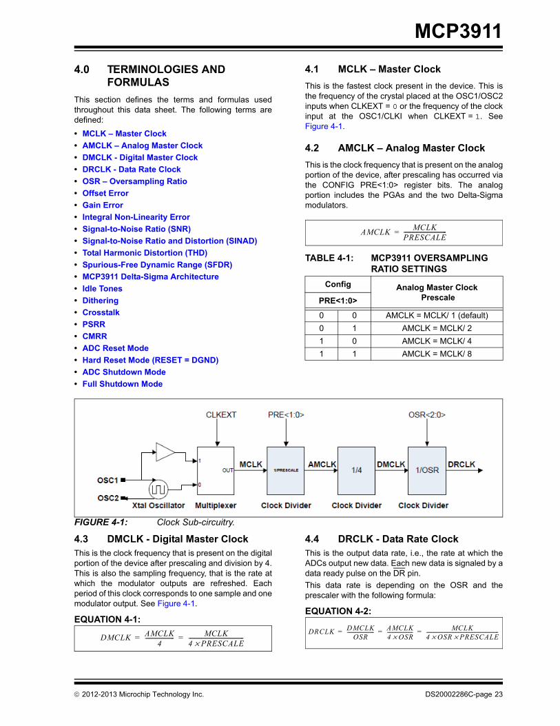
This is the fastest clock present in the device. This isthe frequency of the crystal placed at the OSC1/OSC2inputs when CLKEXT = 0 or the frequency of the clockinput at the OSC1/CLKI when CLKEXT = 1. SeeFigure 4-1.
4.2 AMCLK – Analog Master Clock
This is the clock frequency that is present on the analogportion of the device, after prescaling has occurred viathe CONFIG PRE<1:0> register bits. The analogportion includes the PGAs and the two Delta-Sigmamodulators.
FIGURE 4-1: Clock Sub-circuitry.
4.3 DMCLK - Digital Master ClockThis is the clock frequency that is present on the digitalportion of the device after prescaling and division by 4.This is also the sampling frequency, that is the rate atwhich the modulator outputs are refreshed. Eachperiod of this clock corresponds to one sample and onemodulator output. See Figure 4-1.
EQUATION 4-1:
4.4 DRCLK - Data Rate ClockThis is the output data rate, i.e., the rate at which theADCs output new data. Each new data is signaled by adata ready pulse on the DR pin.
This data rate is depending on the OSR and theprescaler with the following formula:
EQUATION 4-2:
TABLE 4-1: MCP3911 OVERSAMPLING RATIO SETTINGS
Config Analog Master Clock Prescale PRE<1:0>
0 0 AMCLK = MCLK/ 1 (default)
0 1 AMCLK = MCLK/ 2
1 0 AMCLK = MCLK/ 4
1 1 AMCLK = MCLK/ 8
AMCLKMCLK
PRESCALE-------------------------------=
DMCLK AMCLK4
--------------------- MCLK4 PRESCALE×----------------------------------------= =
DRCLK DMCLKOSR
---------------------- AMCLK4 OSR×--------------------- MCLK
4 OSR PRESCALE××-----------------------------------------------------------= = =
2012-2013 Microchip Technology Inc. DS20002286C-page 23

MCP3911
Since this is the output data rate and the decimationfilter is a SINC (or notch) filter, there is a notch in thefilter transfer function at each integer multiple of thisrate.
The following table describes the various combinationsof OSR and PRESCALE and their associated AMCLK,DMCLK and DRCLK rates.
TABLE 4-2: DEVICE DATA RATES IN FUNCTION OF MCLK, OSR, AND PRESCALE, MCLK = 4 MHz
PRE<1:0>
OSR <2:0> OSR AMCLK DMCLK DRCLKDRCLK(ksps)
SINAD(dB)
Note 1
ENOB from
SINAD(bits)
Note 1
1 1 1 1 1 4096 MCLK/8 MCLK/32 MCLK/131072 0.035 98 16
1 1 1 1 1 2048 MCLK/8 MCLK/32 MCLK/65536 0.061 98 16
1 1 1 1 1 1024 MCLK/8 MCLK/32 MCLK/32768 0.122 97 15.8
1 1 1 1 1 512 MCLK/8 MCLK/32 MCLK/16384 0.244 96 15.6
1 1 0 1 1 256 MCLK/8 MCLK/32 MCLK/8192 0.488 95 15.5
1 1 0 1 0 128 MCLK/8 MCLK/32 MCLK/4096 0.976 90 14.7
1 1 0 0 1 64 MCLK/8 MCLK/32 MCLK/2048 1.95 83 13.5
1 1 0 0 0 32 MCLK/8 MCLK/32 MCLK/1024 3.9 70 11.3
1 0 1 1 1 4096 MCLK/4 MCLK/16 MCLK/65536 0.061 98 16
1 0 1 1 1 2048 MCLK/4 MCLK/16 MCLK/32768 0.122 98 16
1 0 1 1 1 1024 MCLK/4 MCLK/16 MCLK/16384 0.244 97 15.8
1 0 1 1 1 512 MCLK/4 MCLK/16 MCLK/8192 0.488 96 15.6
1 0 0 1 1 256 MCLK/4 MCLK/16 MCLK/4096 0.976 95 15.5
1 0 0 1 0 128 MCLK/4 MCLK/16 MCLK/2048 1.95 90 14.7
1 0 0 0 1 64 MCLK/4 MCLK/16 MCLK/1024 3.9 83 13.5
1 0 0 0 0 32 MCLK/4 MCLK/16 MCLK/512 7.8125 70 11.3
0 1 1 1 1 4096 MCLK/2 MCLK/8 MCLK/32768 0.122 98 16
0 1 1 1 1 2048 MCLK/2 MCLK/8 MCLK/16384 0.244 98 16
0 1 1 1 1 1024 MCLK/2 MCLK/8 MCLK/8192 0.488 97 15.8
0 1 1 1 1 512 MCLK/2 MCLK/8 MCLK/4096 0.976 96 15.6
0 1 0 1 1 256 MCLK/2 MCLK/8 MCLK/2048 1.95 95 15.5
0 1 0 1 0 128 MCLK/2 MCLK/8 MCLK/1024 3.9 90 14.7
0 1 0 0 1 64 MCLK/2 MCLK/8 MCLK/512 7.8125 83 13.5
0 1 0 0 0 32 MCLK/2 MCLK/8 MCLK/256 15.625 70 11.3
0 0 1 1 1 4096 MCLK MCLK/4 MCLK/16384 0.244 98 16
0 0 1 1 0 2048 MCLK MCLK/4 MCLK/8192 0.488 98 16
0 0 1 0 1 1024 MCLK MCLK/4 MCLK/4096 0.976 97 15.8
0 0 1 0 0 512 MCLK MCLK/4 MCLK/2048 1.95 96 15.6
0 0 0 1 1 256 MCLK MCLK/4 MCLK/1024 3.9 95 15.5
0 0 0 1 0 128 MCLK MCLK/4 MCLK/512 7.8125 90 14.7
0 0 0 0 1 64 MCLK MCLK/4 MCLK/256 15.625 83 13.5
0 0 0 0 0 32 MCLK MCLK/4 MCLK/128 31.25 70 11.3
Note 1: For OSR = 32 and 64, DITHER = None. For OSR = 128 and higher, DITHER = Maximum. The SINADvalues are given from GAIN = 1.
DS20002286C-page 24 2012-2013 Microchip Technology Inc.
MCP3911
4.5 OSR – Oversampling Ratio
This is the ratio of the sampling frequency to the outputdata rate. OSR = DMCLK/DRCLK. The default OSR is256 or with MCLK = 4 MHz, PRESCALE = 1,AMCLK = 4 MHz, fS = 1 MHz, fD = 3.90625 ksps. Thefollowing bits in the CONFIG register are used tochange the oversampling ratio (OSR).
4.6 Offset Error
This is the error induced by the ADC when the inputsare shorted together (VIN = 0V). The specificationincorporates both PGA and ADC offset contributions.This error varies with PGA and OSR settings. Theoffset is different on each channel and varies from chipto chip. The offset is specified in µV. The offset errorcan be digitally compensated independently on eachchannel through the OFFCAL registers with a 24-bitcalibration word.
The offset on the MCP3911 has a low temperaturecoefficient (see Section 2.0, Typical PerformanceCurves for more information, see Figure 2-33).
4.7 Gain Error
This is the error induced by the ADC on the slope of thetransfer function. It is the deviation expressed inpercentage (%) compared to the ideal transfer functiondefined by Equation 5-3. The specificationincorporates both PGA and ADC gain errorcontributions but not the VREF contribution (it ismeasured with an external VREF).
This error varies with PGA and OSR settings. The gainerror can be digitally compensated independently oneach channel through the GAINCAL registers with a24-bit calibration word.
The gain error on the MCP3911 has a low temperaturecoefficient. For more information, see Figure 2-34.
4.8 Integral Non-Linearity Error
Integral non-linearity error is the maximum deviation ofan ADC transition point from the corresponding point ofan ideal transfer function, with the offset and gainerrors removed or with the end points equal to zero.
It is the maximum remaining error after the calibrationof offset and gain errors for a DC input signal.
4.9 Signal-to-Noise Ratio (SNR)
For the MCP3911 ADCs, the signal-to-noise ratio is aratio of the output fundamental signal power to thenoise power (not including the harmonics of the signal),when the input is a sinewave at a predeterminedfrequency. It is measured in dB. Usually, only themaximum signal-to-noise ratio is specified. The SNRfigure depends mainly on the OSR and DITHERsettings of the device.
EQUATION 4-3: SIGNAL-TO-NOISE RATIO
4.10 Signal-to-Noise Ratio and Distortion (SINAD)
The most important figure of merit for the analogperformance of the ADCs present on the MCP3911 isthe Signal-to-Noise and Distortion (SINAD)specification.
Signal-to-noise and distortion ratio is similar tosignal-to-noise ratio, with the exception that you mustinclude the harmonics power in the noise powercalculation. The SINAD specification depends mainlyon the OSR and DITHER settings.
EQUATION 4-4: SINAD EQUATION
The calculated combination of SNR and THD per thefollowing formula also yields SINAD:
EQUATION 4-5: SINAD, THD, AND SNR RELATIONSHIP
4.11 Total Harmonic Distortion (THD)
The total harmonic distortion is the ratio of the output
harmonics power to the fundamental signal power for asinewave input and is defined by Equation 4-6.
TABLE 4-3: MCP3911 OVERSAMPLING RATIO SETTINGS
Config Oversampling Ratio OSR
OSR<2:0>
0 0 0 32
0 0 1 64
0 1 0 128
0 1 1 256 (DEFAULT)
1 0 0 512
1 0 1 1024
1 1 0 2048
1 1 1 4096
SNR dB( ) 10SignalPowerNoisePower---------------------------------- log=
SINAD dB( ) 10SignalPower
Noise HarmonicsPower+--------------------------------------------------------------------- log=
SINAD dB( ) 10 10
SNR10
-----------
10
THD–10
----------------
+log=
2012-2013 Microchip Technology Inc. DS20002286C-page 25
MCP3911
EQUATION 4-6:
The THD calculation includes the first 35 harmonics forthe MCP3911 specifications. The THD is usually onlymeasured with respect to the 10 first harmonics. THDis sometimes expressed in percentage (%).Equation 4-7 converts the THD in percentage (%):
EQUATION 4-7:
This specification depends mainly on the DITHERsetting.
4.12 Spurious-Free Dynamic Range (SFDR)
The ratio between the output power of the fundamentaland the highest spur in the frequency spectrum. Thespur frequency is not necessarily a harmonic of thefundamental, even though it is usually the case. Thisfigure represents the dynamic range of the ADC whena full-scale signal is used at the input. This specificationdepends mainly on the DITHER setting.
EQUATION 4-8:
4.13 MCP3911 Delta-Sigma Architecture
The MCP3911 incorporates two Delta-Sigma ADCswith a multi-bit architecture. A Delta-Sigma ADC is anoversampling converter that incorporates a built-inmodulator, which is digitizing the quantity of chargeintegrated by the modulator loop (see Figure 5-1). Thequantizer is the block that is performing theanalog-to-digital conversion. The quantizer is typically1-bit or a simple comparator which helps to maintainthe linearity performance of the ADC (the DACstructure in this case is inherently linear).
Multi-bit quantizers help lower the quantization error(the error fed back in the loop can be very large with1-bit quantizers) without changing the order of themodulator or the OSR, which leads to better SNRfigures. However, typically, the linearity of sucharchitectures is more difficult to achieve since the DACis complicated and its linearity limits the THD of suchADCs.
The MCP3911’s five-level quantizer is a flash ADCcomposed of four comparators arranged with equallyspaced thresholds and a thermometer coding. TheMCP3911 also includes proprietary five-level DACarchitecture that is inherently linear for improved THDfigures.
4.14 Idle Tones
A Delta-Sigma converter is an integrating converter. Italso has a finite quantization step Least SignificantByte (LSB) which can be detected by its quantizer. ADC input voltage that is below the quantization stepshould only provide an all zeros result since the input isnot large enough to be detected. As an integratingdevice, any Delta-Sigma shows idle tones in this case.This means that the output will have spurs in thefrequency content that are depending on the ratiobetween quantization step voltage and the inputvoltage. These spurs are the result of the integratedsub-quantization step inputs that eventually cross thequantization steps after a long enough integration. Thisinduces an AC frequency at the output of the ADC andcan be shown in the ADC output spectrum.
These idle tones are residues that are inherent to thequantization process and the fact that the converter isintegrating at all times without being reset. They areresidues of the finite resolution of the conversionprocess. They are very difficult to attenuate and theyare heavily signal dependent. They can degrade bothSFDR and THD of the converter even for DC inputs.They can be localized in the baseband of the converterand thus difficult to filter from the actual input signal.
For power metering applications, idle tones can be verydisturbing because energy can be detected even at the50 or 60 Hz frequency, depending on the DC offset ofthe ADCs, while no power is really present at theinputs. The only practical way to suppress or attenuateidle tones phenomenon is to apply dithering to theADC. The idle tones amplitudes are a function of theorder of the modulator, the OSR and the number oflevels in the quantizer of the modulator. A higher order,a higher OSR or a higher number of levels for thequantizer attenuate the idle tones amplitude.
THD dB( ) 10HarmonicsPower
FundamentalPower----------------------------------------------------- log=
THD %( ) 100 10THD dB( )
20------------------------
×=
SFDR dB( ) 10FundamentalPowerHighestSpurPower----------------------------------------------------- log=
DS20002286C-page 26 2012-2013 Microchip Technology Inc.

MCP3911
4.15 Dithering
To suppress or attenuate the idle tones present in anyDelta-Sigma ADCs, dithering can be applied to theADC. Dithering is the process of adding an error to theADC feedback loop to “decorrelate” the outputs and“break” the idle tones behavior. Usually, a random orpseudo-random generator adds an analog or digitalerror to the feedback loop of the Delta-Sigma ADC toensure that no tonal behavior can happen at its outputs.This error is filtered by the feedback loop and typicallyhas a zero average value, so that the converter statictransfer function is not disturbed by the ditheringprocess. However, the dithering process slightlyincreases the noise floor (it adds noise to the part) whilereducing its tonal behavior and thus improving SFDRand THD (see Figure 2-14 and Figure 2-18). Thedithering process scrambles the idle tones intobaseband white noise and ensures that dynamic specs(SNR, SINAD, THD, SFDR) are less signal dependent.The MCP3911 incorporates a proprietary ditheringalgorithm on both ADCs to remove idle tones andimprove THD, which is crucial for power meteringapplications.
4.16 Crosstalk
The crosstalk is defined as the perturbation caused byone ADC channel on the other ADC channel. It is ameasurement of the isolation between the two ADCspresent in the chip.
This measurement is a two-step procedure:
1. Measure one ADC input with no perturbation onthe other ADC (ADC inputs shorted).
2. Measure the same ADC input with aperturbation sine wave signal on the other ADCat a certain predefined frequency.
The crosstalk is then the ratio between the outputpower of the ADC when the perturbation is present andwhen it is not divided by the power of the perturbationsignal.
A lower crosstalk value implies more independenceand isolation between the two channels.
The measurement of this signal is performed under thedefault conditions at MCLK = 4 MHz:
• GAIN = 1
• PRESCALE = 1
• OSR = 256
• MCLK = 4 MHz
Step 1
• CH0+=CH0- = AGND
• CH1+=CH1- = AGND
Step 2
• CH0+=CH0- = AGND
• CH1+ - CH1- = 1.2VP-P at 50/60 Hz (Full-scale sine wave)
The crosstalk is then calculated with the followingformula:
EQUATION 4-9:
4.17 PSRR
This is the ratio between a change in the power supplyvoltage and the ADC output codes. It measures theinfluence of the power supply voltage on the ADCoutputs.
The PSRR specification can be DC (the power supplyis taking multiple DC values) or AC (the power supplyis a sinewave at a certain frequency with a certaincommon mode). In AC, the amplitude of the sinewaveis representing the change in the power supply. It isdefined in Equation 4-10:
EQUATION 4-10:
Where VOUT is the equivalent input voltage that theoutput code translates to the ADC transfer function. Inthe MCP3911 specification, AVDD varies from 2.7V to3.6V. For AC PSRR, a 50/60 Hz sinewave is chosen,centered around 3.3V with a maximum 300 mVamplitude. The PSRR specification is measured withAVDD = DVDD.
4.18 CMRR
This is the ratio between a change in thecommon-mode input voltage and the ADC outputcodes. It measures the influence of the common-modeinput voltage on the ADC outputs.
The CMRR specification can be DC (thecommon-mode input voltage is taking multiple DCvalues) or AC (the common-mode input voltage is asinewave at a certain frequency with a certain commonmode). In AC, the amplitude of the sinewave isrepresenting the change in the power supply. It isdefined in Equation 4-11:
EQUATION 4-11:
Where VCM = (CHn+ + CHn-)/2 is the common-modeinput voltage and VOUT is the equivalent input voltagethat the output code translates to using the ADCtransfer function. In the MCP3911 specification, VCMvaries from -1V to +1V.
CTalk dB( ) 10ΔCH0PowerΔCH1Power--------------------------------- log=
PSRR dB( ) 20ΔVOUT
ΔAVDD------------------- log=
CMRR dB( ) 20ΔVOUT
ΔVCM----------------- log=
2012-2013 Microchip Technology Inc. DS20002286C-page 27

MCP3911
4.19 ADC Reset Mode
ADC Reset mode (also called Soft Reset mode) canonly be entered through setting high the RESET<1:0>bits in the Configuration register. This mode is definedas the condition where the converters are active, buttheir output is forced to ‘0’.
The registers are not affected in this Reset mode andretain their state, except the data registers of thecorresponding channel, which are reset to ‘0’.
The ADCs can immediately output meaningful codesafter leaving the Reset mode (and after the sinc filtersettling time). This mode is both entered and exitedthrough setting of bits in the Configuration register.
Each converter can be placed in Soft Reset modeindependently. The configuration registers are notmodified by the Soft Reset mode.
A data ready pulse is not generated by any ADC whilein Reset mode.
Reset mode also affects the modulator output block,i.e., the MDAT pin, corresponding to the channel inReset. If enabled, it provides a bit streamcorresponding to a zero output (a series of 0011 bitscontinuously repeated).
When an ADC exits the ADC Reset mode, any phasedelay present before reset was entered is still present.If one ADC is not in Reset mode, the ADC leaving theReset mode automatically resynchronizes the phasedelay relative to the other ADC channel per the phasedelay register block and gives data ready pulsesaccordingly.
If an ADC is placed in Reset mode while the other isconverting, it is not shutting down the internal clock.When going back out of Reset, it is automaticallyresynchronized with the clock that did not stop duringReset.
If both ADCs are in Soft Reset, the clock is no longerdistributed to the digital core for low-power operation.Once any of the ADC is back to normal operation, theclock is automatically distributed again.
However, when the two channels are in Soft Reset, theinput structure is still clocking if MCLK is applied toproperly bias the inputs so that no leakage current isobserved. If MCLK is not applied, large analog inputleakage currents can be observed for highly negativeinput voltages (typically below -0.6V referred to AGND).
4.20 Hard Reset Mode (RESET = DGND)
This mode is only available during a POR or when theRESET pin is pulled low. The RESET pin low stateplaces the device in a Hard Reset mode.
In this mode, all internal registers are reset to theirdefault state.
The DC biases for the analog blocks are still active, i.e.the MCP3911 is ready to convert. However, this pinclears all conversion data in the ADCs. In this mode,the MDAT outputs are in high-impedance. Thecomparator’s outputs of both ADCs are forced to theirreset state (0011). The SINC filters are all reset as wellas their double output buffers. See serial timing forminimum pulse low time in Section 1.0 “ElectricalCharacteristics”.
During a Hard Reset, no communication with the part ispossible. The digital interface is maintained in a resetstate.
In this state, to properly bias the input structures of bothchannels, the MCLK can be applied to the part. If notapplied, large analog input leakage currents can beobserved for highly negative input signals, and afterremoving the RESET state, a certain start-up time isnecessary to bias the input structure properly. Duringthis delay, the ADC conversions can be inaccurate.
4.21 ADC Shutdown Mode
ADC Shutdown mode is defined as a state where theconverters and their biases are off, consuming onlyleakage current. When the Shutdown bit is reset to ‘0’,the analog biases are enabled as well as the clock andthe digital circuitry. The ADC gives a data ready pulseafter the SINC filter settling time has occurred.However, since the analog biases are not completelysettled at the beginning of the conversion, the samplingmay not be accurate during about 1 ms (correspondingto the settling time of the biasing in worst caseconditions). To ensure the accuracy, the data readypulse coming within the delay of 1 ms + settling time ofthe SINC filter should be discarded.
Each converter can be placed in Shutdown modeindependently. The CONFIG registers are not modifiedby the Shutdown mode. This mode is only availablethrough programming of the SHUTDOWN<1:0> bitsthe CONFIG register.
The output data is flushed to all zeros while in ADCShutdown mode. No data ready pulses are generatedby any ADC while in ADC Shutdown mode.
ADC Shutdown mode also affects the modulator outputblock, i.e. if MDAT of the channel in Shutdown mode isenabled, this pin provides a bit stream corresponding toa zero output (series of 0011 bits continuouslyrepeated).
DS20002286C-page 28 2012-2013 Microchip Technology Inc.

MCP3911
When an ADC exits ADC Shutdown mode, any phasedelay present before shutdown was entered is stillpresent. If one ADC was not in Shutdown mode, theADC exiting Shutdown mode automaticallyresynchronizes the phase delay relative to the otherADC channel, per the phase delay register block andgive data ready pulses accordingly.
If an ADC is placed in Shutdown mode while the otheris converting, the internal clock is not shut down. Whenexiting Shutdown mode, the ADC is automaticallyresynchronized with the clock that did not stop duringReset.
If both ADCs are in Shutdown mode, the clock is nolonger distributed to the input structure or to the digitalcore for low power operation. If the input voltage ishighly negative (typically below -0.6V, referred toAGND), this can cause potential high analog inputleakage currents at the analog inputs. Once any of theADC is back to normal operation, the clock isautomatically distributed again.
4.22 Full Shutdown Mode
The lowest power consumption can be achieved whenSHUTDOWN<1:0> = 11, VREFEXT = CLKEXT = 1.This mode is called Full Shutdown mode, and noanalog circuitry is enabled. In this mode, both AVDDand DVDD POR monitoring are also disabled. No clockis propagated throughout the chip. Both ADCs are inShutdown, and the internal voltage reference isdisabled.
The clock is not distributed to the input structure anylonger. This can cause potential high analog inputsleakage currents at the analog inputs, if the inputvoltage is highly negative (typically below -0.6V,referred to AGND).
The only circuit that remains active is the SPI interface,but this circuit does not induce any static powerconsumption. If SCK is idle, the only currentconsumption comes from the leakage currents inducedby the transistors and is less than 1 µA on each powersupply.
This mode can be used to power down the chipcompletely and avoid power consumption when thereis no data to convert at the analog inputs. Any SCK orMCLK edge coming while in this mode inducesdynamic power consumption.
Once any of the SHUTDOWN, CLKEXT and VREFEXTbits return to ‘0’, the two POR monitoring blocks areback to operation, and AVDD and DVDD monitoring cantake place.
When exiting full Shutdown mode, the device resets toits default configuration state. The Configuration bits allreset to their default value, and the ADCs reset to theirinitial state, requiring three DRCLK periods for an initialdata ready pulse. Exiting full Shutdown mode iseffectively identical to an internal reset or returningfrom a POR condition.
2012-2013 Microchip Technology Inc. DS20002286C-page 29

MCP3911
NOTES:
DS20002286C-page 30 2012-2013 Microchip Technology Inc.

MCP3911
5.0 DEVICE OVERVIEW
5.1 Analog Inputs (CHn+/-)
The MCP3911 analog inputs can be connected directlyto current and voltage transducers (such as shunts,current transformers or Rogowski coils). Each input pinis protected by specialized ESD structures that arecertified to pass 4.0 kV HBM and 300V MM contactcharge. These structures allow bipolar ±2V continuousvoltage with respect to AGND to be present at theirinputs without the risk of permanent damage.
Both channels have fully differential voltage inputs forbetter noise performance. The absolute voltage at eachpin relative to AGND should be maintained in the ±1Vrange during operation to ensure the specified ADCaccuracy. The common-mode signals should beadapted to respect both the previous conditions andthe differential input voltage range. For bestperformance, the common-mode signals should bemaintained to AGND.
5.2 Programmable Gain Amplifiers (PGA)
The two Programmable Gain Amplifiers (PGAs) resideat the front-end of each Delta-Sigma ADC. They havetwo functions: translate the common-mode of the inputfrom AGND to an internal level between AGND andAVDD, and amplify the input differential signal. Thetranslation of the common mode does not change thedifferential signal, but recenters the common-mode sothat the input signal can be properly amplified.
The PGA block can be used to amplify very low signals,but the differential input range of the Delta-Sigmamodulator must not be exceeded. The PGA iscontrolled by the PGA_CHn<2:0> bits in the GAINregister. The following table represents the gainsettings for the PGA:
5.3 Delta-Sigma Modulator
5.3.1 ARCHITECTURE
Both ADCs are identical in the MCP3911 and theyinclude a proprietary second-order modulator with amulti-bit five-level DAC architecture (see Figure 5-1).The quantizer is a flash ADC composed of fourcomparators with equally spaced thresholds and athermometer output coding. The proprietary five-levelarchitecture ensures minimum quantization noise atthe outputs of the modulators without disturbinglinearity or inducing additional distortion. The samplingfrequency is DMCLK (typically 1 MHz withMCLK = 4 MHz), so the modulator outputs arerefreshed at a DMCLK rate. The modulator outputs areavailable in the MOD register or serially transferred oneach MDAT pin.
Figure 5-1 represents a simplified block diagram of theDelta-Sigma ADC present on MCP3911.
FIGURE 5-1: Simplified Delta-Sigma ADC Block Diagram.
Note: If the analog inputs are held to a potentialof -0.6 to -1V for extended periods of time,MCLK must be present inside the deviceto avoid large leakage currents at theanalog inputs. This is true even during theHard or Soft Reset mode of both ADCs. However, during the Shutdown mode ofthe two ADCs or POR state, the clock isnot distributed inside the circuit. Duringthese states, it is recommended to keepthe analog input voltages above -0.6Vreferred to AGND to avoid high analoginputs leakage currents.
TABLE 5-1: PGA CONFIGURATION SETTING
Gain PGA_CHn<2:0>
Gain(V/V)
Gain(dB)
VIN Range (V)
0 0 0 1 0 ±0.6
0 0 1 2 6 ±0.3
0 1 0 4 12 ±0.15
0 1 1 8 18 ±0.075
1 0 0 16 24 ±0.0375
1 0 1 32 30 ±0.01875
Note: This table is defined with VREF = 1.2V. Thetwo undefined settings, 110 and 111 areG = 1.
Second-Order
Integrator
LoopFilter
Quantizer
DAC
Differential
Voltage Input
Output
Bitstreamfive-level
Flash ADC
MCP3911 Delta-Sigma Modulator
2012-2013 Microchip Technology Inc. DS20002286C-page 31

MCP3911
5.3.2 MODULATOR INPUT RANGE AND SATURATION POINT
For a specified voltage reference value of 1.2V, themodulator’s specified differential input range is±600 mV. The input range is proportional to VREF andscales according to the VREF voltage. This range isensuring the stability of the modulator over amplitudeand frequency. Outside of this range, the modulator isstill functional. However, its stability is no longerensured and therefore it is not recommended to exceedthis limit. See Figure 2-24 for extended dynamic rangeperformance limitations. The saturation point for themodulator is VREF/1.5, since the transfer function of theADC includes a gain of 1.5 by default (independentfrom the PGA setting. See Section 5.6 “ADC OutputCoding”).
5.3.3 BOOST SETTINGS
The Delta-Sigma modulators include a programmablebiasing circuit to further adjust the power consumptionto the sampling speed applied through the MCLK. Thiscan be programmed through the BOOST<1:0> bits,which are applied to both channels simultaneously.
The maximum achievable analog master clock speed(AMCLK) and the maximum sampling frequency(DMCLK) and therefore, the maximum achievable datarate (DRCLK), highly depend on BOOST<1:0> andPGA_CHn<2:0> settings. Table 5-2 specifies themaximum AMCLK possible to keep optimal accuracy infunction of BOOST<1:0> and PGA_CHn<2:0>settings.
TABLE 5-2: MAXIMUM AMCLK LIMITS AS A FUNCTION OF BOOST AND PGA GAIN
Conditions VDD = 3.0V to 3.6V, TA from -40°C to +125°C VDD = 2.7V to 3.6V, TA from -40°C to +125°C
Boost Gain Maximum AMCLK (MHz)
(SINAD within -3 dB from its maximum)
Maximum AMCLK (MHz)
(SINAD within -5 dB from its maximum)
Maximum AMCLK (MHz)
(SINAD within -3 dB from its maximum)
Maximum AMCLK (MHz)
(SINAD within -5 dB from its maximum)
0.5x 1 3 3 3 3
0.66x 1 4 4 4 4
1x 1 10 10 10 10
2x 1 16 16 16 16
0.5x 2 2.5 3 3 3
0.66x 2 4 4 4 4
1x 2 10 10 10 10
2x 2 14.5 16 13.3 14.5
0.5x 4 2.5 2.5 2.5 2.5
0.66x 4 4 4 4 4
1x 4 10 10 8 10
2x 4 13.3 16 10.7 11.4
0.5x 8 2.5 2.5 2.5 2.5
0.66x 8 4 4 4 4
1x 8 10 11.4 6.7 8
2x 8 10 14.5 8 8
0.5x 16 2 2 2 2
0.66x 16 4 4 4 4
1x 16 10.6 10.6 8 10
2x 16 12.3 16 8 10.7
0.5x 32 2 2 2 2
0.66x 32 4 4 4 4
1x 32 10 11.4 8 10
2x 32 13.3 16 8 10
DS20002286C-page 32 2012-2013 Microchip Technology Inc.

MCP3911
5.3.4 AUTOZEROING FREQUENCY SETTING (AZ_FREQ)
The MCP3911 modulators include an auto-zeroingalgorithm to improve the offset error performance andgreatly diminish 1/f noise in the ADC. This algorithmallows the device to reach very high SNR and flattensthe noise spectrum at the output of the ADC (seeperformance graphs Figure 2-1, Figure 2-2, Figure 2-3and Figure 2-4). This auto-zeroing algorithm isperformed synchronously with the MCLK coming to thedevice. Its rate can be adjusted throughout theAZ_FREQ bit in the CONFIG register.
When AZ_FREQ = 0 (default), the auto-zeroing occursat the slowest rate, which diminishes the 1/f noise whilenot impacting the THD performance. This mode isrecommended for low values of the PGA gain(GAIN = 1x or 2x).
When AZ_FREQ = 1, the auto-zeroing occurs at thefastest rate, which further diminishes the 1/f noise andfurther improves the SNR, especially at higher gainsettings. The THD may slightly be impacted in thismode (see Figure 2-22). This mode is recommendedfor higher PGA gain settings to improve SNR (GAINsuperior or equal to 4x).
5.3.5 DITHER SETTINGS
Both modulators also include a dithering algorithm thatcan be enabled through the DITHER<1:0> bits in theconfiguration register. This dithering process improvesTHD and SFDR (for high OSR settings) whileincreasing slightly the noise floor of the ADCs. Forpower metering applications and applications that aredistortion-sensitive, it is recommended to keepDITHER at maximum settings for best THD and SFDRperformance. In the case of power-meteringapplications, THD and SFDR are critical specifications.Optimizing SNR (noise floor) is not really problematicdue to large averaging factor at the output of the ADCs.Therefore, even for low OSR settings, the ditheringalgorithm shows a positive impact on the performanceof the application.
5.4 Modulator Output Block
If the user wishes to use the modulator output of thedevice, the appropriate bits to enable the modulatoroutput must be set in the Configuration register.
When MODOUT<1:0> bits are enabled, the modulatoroutput of the corresponding channel is present at thecorresponding MDAT output pin as soon as thecommand is placed. Additionally, the correspondingSINC filter is disabled to consume less current. Thecorresponding DR pulse is also not present at the DRoutput pin. When MODOUT<1:0> bits are cleared, thecorresponding SINC filters are back to normaloperation and the corresponding MDAT outputs are inhigh-impedance.
Since the Delta-Sigma modulators have a five-leveloutput given by the state of four comparators withthermometer coding, their outputs can be representedon four bits, each bit giving the state of thecorresponding comparator (see Table 5-3). These bitsare present on the MOD register and are updated at theDMCLK rate.
To output the comparator’s result on a separate pin(MDAT0 and MDAT1), these comparator output bitshave been arranged to be serially output at the AMCLKrate (see Figure 5-2).
This 1-bit serial bit stream is identical to the oneproduced by a 1-bit DAC modulator with a samplingfrequency of AMCLK. The modulator can eitheroperate as five level output at DMCLK rate or a 1-bitoutput at AMCLK rate. These two representations areinterchangeable. The MDAT outputs can therefore beused in any application that requires 1-bit modulatoroutputs. These applications often integrate and filterthe 1-bit output with SINC or more complex decimationfilters computed by an MCU or DSP.
TABLE 5-3: DELTA-SIGMA MODULATOR CODING
Comp<3:0> Code
Modulator Output Code
MDAT Serial Stream
1111 +2 1111
0111 +1 0111
0011 0 0011
0001 -1 0001
0000 -2 0000
2012-2013 Microchip Technology Inc. DS20002286C-page 33

MCP3911
FIGURE 5-2: MDAT Serial Outputs in Function of the Modulator Output Code.
Since the Reset and Shutdown SPI commands areasynchronous, the MDAT pins are resynchronized withDMCLK after each time the part goes out of Reset andShutdown.
This means that the first output of MDAT, after a SoftReset or a Shutdown, is always 0011 after the firstDMCLK rising edge.
The two MDAT output pins are in high-impedance if theRESET pin is low.
5.5 SINC3 + SINC1 Filter
The decimation filter present in both channels of theMCP3911 is a cascade of two sinc filters (sinc3+sinc1):a third order sinc filter with a decimation ratio of OSR3followed by first order sinc filter with a decimation ratioof OSR1 (moving average of OSR1 values). Figure 5-3represents the decimation filter architecture.
FIGURE 5-3: MCP3911 Decimation Filter Block Diagram.
Equation 5-1 contains the formula for calculating thetransfer function of the digital decimation filter andsettling time of the ADC:
EQUATION 5-1: SINC FILTER TRANSFER FUNCTION
EQUATION 5-2: SETTING TIME OF THE ADC AS A FUNCTION OF DMCLK PERIODS
DMCLK
MDAT+2
MDAT+1
MDAT+0
MDAT-1
MDAT-2
COMP
AMCLK
<3>COMP
<2>COMP
<1>COMP
<0>
ModulatorOutput
SINC3 SINC1 Decimation Filter Output
OSR3 OSR1
416 (WIDTH=0)24 (WIDTH=1)
Decimation Filter
OSR1=1
H z( )1 z
- OSR3–
3
OSR3 1 z 1––( )( )3----------------------------------------------
1 z- OSR1 OSR3×
–
OSR1 1 z- OSR3–
×---------------------------------------------------------×=
Where z EXP 2π j fin⋅ ⋅ DMCLK⁄( )=
SettlingTime DMCLKPeriods( ) 3 OSR3× OSR1 1–( ) OSR3×+=
DS20002286C-page 34 2012-2013 Microchip Technology Inc.

MCP3911
The SINC1 filter following the SINC3 filter is onlyenabled for the high OSR settings. This SINC1 filterprovides additional rejection at a low cost with littlemodification to the -3 dB bandwidth. For 24-Bit Outputmode (WIDTH = 1), the output of the sinc filter ispadded on the right with least significant zeros, up to24 bits, for any resolution less than 24 bits. For 16-BitOutput modes, the output of the sinc filter is rounded tothe closest 16-bit number, to conserve only 16-bitwords and to minimize truncation error.
The gain of the transfer function of this filter is 1 at eachmultiple of DMCLK (typically 1 MHz), so a proper anti-aliasing filter must be placed at the inputs. Thisattenuates the frequency content around DMCLK andkeep the desired accuracy over the baseband of theconverter. This anti-aliasing filter can be a simple, first-order RC network with a sufficiently low-time constantto generate high rejection at DMCLK frequency.
Any unsettled data is automatically discarded to avoiddata corruption. Each data ready pulse corresponds tofully settled data at the output of the decimation filter.The first data available at the output of the decimationfilter is present after the complete settling time of thefilter (see Table 5-4). After the first data has beenprocessed, the delay between two data ready pulses is1/DRCLK. The data stream from input to output isdelayed by an amount equal to the settling time of thefilter (which is the group delay of the filter).
The achievable resolution, the -3 dB bandwidth and thesettling time at the output of the decimation filter (theoutput of the ADC), is dependent on the OSR of eachsinc filter and is summarized in Table 5-4:
FIGURE 5-4: SINC Filter Frequency Response, OSR = 256, MCLK = 4 MHz, PRE<1:0> = 00.
FIGURE 5-5: SINC Filter Frequency Response, OSR = 4096 (pink), OSR = 512 (blue), MCLK = 4 MHz, PRE<1:0> = 00.
TABLE 5-4: OVERSAMPLING RATIO AND SINC FILTER SETTLING TIME
OSR<2:0> OSR3 OSR1 Total OSR Resolution In Bits (No Missing Codes)
Settling Time -3 dB Bandwidth
0 0 0 32 1 32 17 96/DMCLK 0.26*DRCLK
0 0 1 64 1 64 20 192/DMCLK 0.26*DRCLK
0 1 0 128 1 128 23 384/DMCLK 0.26*DRCLK
0 1 1 256 1 256 24 768/DMCLK 0.26*DRCLK
1 0 0 512 1 512 24 1536/DMCLK 0.26*DRCLK
1 0 1 512 2 1024 24 2048/DMCLK 0.37*DRCLK
1 1 0 512 4 2048 24 3072/DMCLK 0.42*DRCLK
1 1 1 512 8 4096 24 5120/DMCLK 0.43*DRCLK
-120
-100
-80
-60
-40
-20
0
1 10 100 1000 10000 100000
Mag
nitu
de (d
B)
Input Frequency (Hz)
-160
-140
-120
-100
-80
-60
-40
-20
0
1 100 10000 1000000
Mag
nitu
de (d
B)
Input Frequency (Hz)
2012-2013 Microchip Technology Inc. DS20002286C-page 35
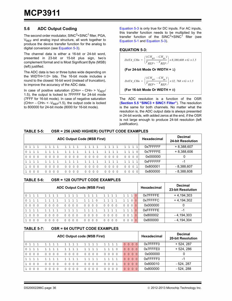
MCP3911
5.6 ADC Output Coding
The second order modulator, SINC3+SINC1 filter, PGA,VREF and analog input structure, all work together toproduce the device transfer function for the analog todigital conversion (see Equation 5-3).
The channel data is either a 16-bit or 24-bit word,presented in 23-bit or 15-bit plus sign, two’scomplement format and is Most Significant Byte (MSB)(left) justified.
The ADC data is two or three bytes wide depending onthe WIDTH<1:0> bits. The 16-bit mode includes around to the closest 16-bit word (instead of truncation),to improve the accuracy of the ADC data.
In case of positive saturation (CHn+ – CHn- > VREF/1.5), the output is locked to 7FFFFF for 24-bit mode(7FFF for 16-bit mode). In case of negative saturation(CHn+ – CHn- < -VREF/1.5), the output code is lockedto 800000 for 24-bit mode (8000 for 16-bit mode).
Equation 5-3 is only true for DC inputs. For AC inputs,this transfer function needs to be multiplied by thetransfer function of the SINC3+SINC1 filter (seeEquation 5-1 and Equation 5-3).
EQUATION 5-3:
The ADC resolution is a function of the OSR(Section 5.5 “SINC3 + SINC1 Filter”). The resolutionis the same for both channels. No matter what theresolution is, the ADC output data is always presentedin 24-bit words, with added zeros at the end, if the OSRis not large enough to produce 24-bit resolution (leftjustification).
DATA_CHnCHn+ CHn-–( )
VREF+ VREF-–-----------------------------------------
8,388,608 G 1.5×××=
DATA_CHnCHn+ CHn-–( )
VREF+ VREF-–-----------------------------------------
32 768, G 1.5×××=
(For 24-bit Mode Or WIDTH = 1)
(For 16-bit Mode Or WIDTH = 0)
TABLE 5-5: OSR = 256 (AND HIGHER) OUTPUT CODE EXAMPLES
ADC Output Code (MSB First) HexadecimalDecimal
24-bit Resolution
0 1 1 1 1 1 1 1 1 1 1 1 1 1 1 1 1 1 1 1 1 1 1 1 0x7FFFFF + 8,388,607
0 1 1 1 1 1 1 1 1 1 1 1 1 1 1 1 1 1 1 1 1 1 1 0 0x7FFFFE + 8,388,606
0 0 0 0 0 0 0 0 0 0 0 0 0 0 0 0 0 0 0 0 0 0 0 0 0x000000 0
1 1 1 1 1 1 1 1 1 1 1 1 1 1 1 1 1 1 1 1 1 1 1 1 0xFFFFFF -1
1 0 0 0 0 0 0 0 0 0 0 0 0 0 0 0 0 0 0 0 0 0 0 1 0x800001 - 8,388,607
1 0 0 0 0 0 0 0 0 0 0 0 0 0 0 0 0 0 0 0 0 0 0 0 0x800000 - 8,388,608
TABLE 5-6: OSR = 128 OUTPUT CODE EXAMPLES
ADC Output Code (MSB First) HexadecimalDecimal
23-bit Resolution
0 1 1 1 1 1 1 1 1 1 1 1 1 1 1 1 1 1 1 1 1 1 1 0 0x7FFFFE + 4,194,303
0 1 1 1 1 1 1 1 1 1 1 1 1 1 1 0 1 1 1 1 1 1 0 0 0x7FFFFC + 4,194,302
0 0 0 0 0 0 0 0 0 0 0 0 0 0 0 0 0 0 0 0 0 0 0 0 0x000000 0
1 1 1 1 1 1 1 1 1 1 1 1 1 1 1 1 1 1 1 1 1 1 1 0 0xFFFFFE -1
1 0 0 0 0 0 0 0 0 0 0 0 0 0 0 0 0 0 0 0 0 0 1 0 0x800002 - 4,194,303
1 0 0 0 0 0 0 0 0 0 0 0 0 0 0 0 0 0 0 0 0 0 0 0 0x800000 - 4,194,304
TABLE 5-7: OSR = 64 OUTPUT CODE EXAMPLES
ADC Output code (MSB First) HexadecimalDecimal
20-bit Resolution
0 1 1 1 1 1 1 1 1 1 1 1 1 1 1 1 1 1 1 1 0 0 0 0 0x7FFFF0 + 524, 287
0 1 1 1 1 1 1 1 1 1 1 1 1 1 1 1 1 1 1 0 0 0 0 0 0x7FFFE0 + 524, 286
0 0 0 0 0 0 0 0 0 0 0 0 0 0 0 0 0 0 0 0 0 0 0 0 0x000000 0
1 1 1 1 1 1 1 1 1 1 1 1 1 1 1 1 1 1 1 1 0 0 0 0 0xFFFFF0 -1
1 0 0 0 0 0 0 0 0 0 0 0 0 0 0 0 0 0 0 1 0 0 0 0 0x800010 - 524, 287
1 0 0 0 0 0 0 0 0 0 0 0 0 0 0 0 0 0 0 0 0 0 0 0 0x800000 - 524, 288
DS20002286C-page 36 2012-2013 Microchip Technology Inc.

MCP3911
5.7 Voltage Reference
5.7.1 INTERNAL VOLTAGE REFERENCE
The MCP3911 contains an internal voltage referencesource specially designed to minimize driftovertemperature. To enable the internal voltagereference, the VREFEXT bit in the configurationregister must be set to ‘0’ (default mode). This internalVREF supplies reference voltage to both channels. Thetypical value of this voltage reference is 1.2V ±2%. Theinternal reference has a very low typical temperaturecoefficient of ±7 ppm/°C, allowing the output to haveminimal variation with respect to temperature, sincethey are proportional to (1/VREF).
The noise of the internal voltage reference is lowenough not to significantly degrade the SNR of theADC if compared to a precision external low-noisevoltage reference. The output pin for the internalvoltage reference is REFIN+/OUT.
If the voltage reference is only used as an internalVREF, adding bypass capacitance on REFIN+/OUT isnot necessary for keeping ADC accuracy, but a minimal0.1 µF ceramic capacitance can be connected to avoidEMI/EMC susceptibility issues, due to the antennacreated by the REFIN+/OUT pin, if left floating.
The bypass capacitors also help applications where thevoltage reference output is connected to other circuits.In this case, additional buffering may be needed, as theoutput drive capability of this output is low.
Adding too much capacitance on the REFIN+/OUT pinmay slightly degrade the THD performance of theADCs.
5.7.2 DIFFERENTIAL EXTERNAL VOLTAGE INPUTS
When the VREFEXT bit is high, the two reference pins(REFIN+/OUT, REFIN-) become a differential voltagereference input. The internal voltage reference circuit isplaced into Shutdown mode and the switch connectingthis circuit to the reference voltage input of the ADC isopened. The internal voltage reference circuit is placedinto Shutdown mode and the switch connecting thiscircuit to the reference voltage input of the ADC isopened. The voltage at the REFIN+/OUT is notedVREF+ and the voltage at the REFIN- pin is noted VREF-. The differential voltage input value is given by thefollowing equation:
EQUATION 5-4:
The specified VREF range is from 1.1V to 1.3V. TheREFIN- pin voltage (VREF-) should be limited to ±0.1V,with respect to AGND. Typically, for single-endedreference applications, the REFIN- pin should bedirectly connected to AGND, with its own separate trackto avoid any spike due to switching noise.
TABLE 5-8: OSR = 32 OUTPUT CODE EXAMPLES
ADC Output code (MSB First) HexadecimalDecimal
17-bit Resolution
0 1 1 1 1 1 1 1 1 1 1 1 1 1 1 1 1 0 0 0 0 0 0 0 0x7FFF80 + 65, 535
0 1 1 1 1 1 1 1 1 1 1 1 1 1 1 1 0 0 0 0 0 0 0 0 0x7FFF00 + 65, 534
0 0 0 0 0 0 0 0 0 0 0 0 0 0 0 0 0 0 0 0 0 0 0 0 0x000000 0
1 1 1 1 1 1 1 1 1 1 1 1 1 1 1 1 1 0 0 0 0 0 0 0 0xFFFF80 -1
1 0 0 0 0 0 0 0 0 0 0 0 0 0 0 0 1 0 0 0 0 0 0 0 0x800080 - 65, 535
1 0 0 0 0 0 0 0 0 0 0 0 0 0 0 0 0 0 0 0 0 0 0 0 0x800000 - 65, 536
VREF = VREF+ – VREF-
2012-2013 Microchip Technology Inc. DS20002286C-page 37

MCP3911
5.7.3 TEMPERATURE COMPENSATION (VREFCAL REGISTER)
The internal voltage reference comprises a proprietarycircuit and algorithm to compensate first order andsecond order temperature coefficients. Thecompensation allows very low temperature coefficients(typically 7 ppm/°C) on the entire range of temperaturesfrom -40°C to +125°C. This temperature coefficient variesfrom part to part.
This temperature coefficient can be adjusted on eachpart through the VREFCAL register (address 0x1A).This register is only for advanced users. This registershould not be written unless the user wants to calibratethe temperature coefficient of the whole system orapplication. The default value of this register is set to0x42. The typical variation of the temperaturecoefficient of the internal voltage reference, withrespect to VREFCAL register code, is shown inFigure 5-6. Modifying the value stored in the VREFCALregister may also vary the output voltage, in addition tothe temperature coefficient.
FIGURE 5-6: VREF Tempco vs. VREFCAL Trimcode Chart.
5.8 Power-on Reset
The MCP3911 contains an internal POR circuit thatmonitors both analog and digital supply voltages duringoperation. The typical threshold for a power-up eventdetection is 2.1V ±5% and a typical start-up time (tPOR)of 50 µs. The POR circuit has a built-in hysteresis forimproved transient spikes immunity that has a typicalvalue of 200 mV. Proper decoupling capacitors (0.1 µFceramic and 10 µF in parallel are sufficient in mostcases) should be mounted as close as possible to theAVDD and DVDD pins, providing additional transientimmunity.
Figure 5-7 illustrates the different conditions atpower-up and a power-down event in typicalconditions. All internal DC biases are not settled until atleast 1 ms, in worst case conditions, after system POR.Any data ready pulse that occurs within 1 ms, plus thesinc filter settling time after system reset, should beignored to ensure proper accuracy. After POR, dataready pulses are present at the pin with all the defaultconditions in the configuration registers.
Both AVDD and DVDD are monitored so either powersupply can sequence first.
FIGURE 5-7: Power-on Reset Operation.
0
10
20
30
40
50
60
0 64 128 192 256
V REF
Drif
t (pp
m)
VREFCAL Register Trim Code (decimal)
PORState
Power-Up Normal PORState
Biases areunsettled.
Conversionsstarted here maynot be accurate.
Biases are settled.Conversions startedhere are accurate.
Analog biasessettling time
SINC filtersettling
time
Voltage(AVDD, DVDD)
Time
POR Thresholdup (2.1V typical)
(1.9V typical)
tPOR
Operation
Any data read pulse occuring during this time can yield inaccurate output data. It is recommended to discard them.
DS20002286C-page 38 2012-2013 Microchip Technology Inc.

MCP3911
5.9 RESET Effect On Delta-Sigma Modulator/SINC Filter
When the RESET pin is logic low, both ADCs are inReset mode and output code 0x0000h. The RESET pinperforms a hard reset (DC biases still on, part ready toconvert) and clears all charges contained in the Delta-Sigma modulators. The comparator’s output is 0011for each ADC.
The SINC filters are all reset, as well as their doubleoutput buffers. This pin is independent of the serialinterface. It brings all the registers to the default state.When RESET is logic low, any write with the SPIinterface is disabled and has no effect. All output pins(SDO, DR, MDAT0/1) are high-impedance.
If MCLK is applied, the input structure is enabled and isproperly biasing the substrate of the input transistors. Ifthe analog inputs are between -1V and +1V, theleakage current on the analog inputs is low.
If MCLK is not applied when in Reset mode, theleakage can be high if the analog inputs are below-0.6V, referred to AGND.
5.10 Phase Delay Block
The MCP3911 incorporates a phase delay generator,which ensures that the two ADCs are converting theinputs with a fixed delay between them. The two ADCsare synchronously sampling, but the averaging ofmodulator outputs is delayed, so that the SINC filteroutputs (thus the ADC outputs), show a fixed phasedelay as determined by the PHASE register’s setting.
The phase value (PHASE<11:0>) is an 11 bit + sign,MSB first, two's complement code that indicates howmuch phase delay there is to be between Channel 0and Channel 1. The four MSB of the first phase register(address 0x07) are undefined and set to ‘0’. Thereference channel for the delay is Channel 1 (typicallythe voltage channel for power metering applications).When PHASE<11:0> is positive, Channel 0 is laggingversus Channel 1. When PHASE<11:0> is negative,Channel 0 is leading versus Channel 1. The amount ofdelay between two ADC conversions is shown inEquation 5-5.
EQUATION 5-5:
The timing resolution of the phase delay is 1/DMCLK,or 1 µs in the default configuration with MCLK = 4 MHz.
The data ready signals are affected by the phase delaysettings. Typically, the time difference between the dataready pulses of Channel 0 and Channel 1 is equal tothe phase delay setting.
5.10.1 PHASE DELAY LIMITS
The Phase delay can only go from -OSR/2 to +OSR/2 - 1. This sets the fine phase resolution. The phaseregister is coded with two's complement.
If larger delays between the two channels are needed,they can be implemented externally to the chip with anMCU. A First In, First Out algorithm (FIFO) in the MCUcan save incoming data from the leading channel for anumber N of DRCLK. In this case, DRCLK representsthe coarse timing resolution and DMCLK representsthe fine timing resolution. The total delay is shown inEquation 5-6.
EQUATION 5-6:
The Phase delay register can be programmed oncewith the OSR = 4096 setting and adjusts to the OSRautomatically afterwards without the need to changethe value of the PHASE register.
• OSR = 4096: the delay can go from -2048 to +2047. PHASE<11> is the sign bit. Phase<10> is the MSB and PHASE<0> the LSB.
• OSR = 2048: the delay can go from -1024 to +1023. PHASE<10> is the sign bit. Phase<9> is the MSB and PHASE<0> the LSB.
• OSR = 1024: the delay can go from -512 to +511. PHASE<9> is the sign bit. Phase<8> is the MSB and PHASE<0> the LSB.
• OSR = 512: the delay can go from -256 to +255. PHASE<8> is the sign bit. Phase<7> is the MSB and PHASE<0> the LSB.
• OSR = 256: the delay can go from -128 to +127. PHASE<7> is the sign bit. Phase<6> is the MSB and PHASE<0> the LSB.
• OSR = 128: the delay can go from -64 to +63. PHASE<6> is the sign bit. Phase<5> is the MSB and PHASE<0> the LSB.
• OSR = 64: the delay can go from -32 to +31. PHASE<5> is the sign bit. Phase<4> is the MSB and PHASE<0> the LSB.
• OSR = 32: the delay can go from -16 to +15. PHASE<4> is the sign bit. Phase<3> is the MSB and PHASE<0> the LSB.
Note: A detailed explanation of the data readypin (DR) with phase delay is shown inFigure 6-9.
Delay Phase Register CodeDMCLK
--------------------------------------------------=
Note: Rewriting the PHASE registers with thesame value resets and automaticallyrestarts both ADCs.
Delay = N/DRCLK + PHASE/DMCLK
2012-2013 Microchip Technology Inc. DS20002286C-page 39
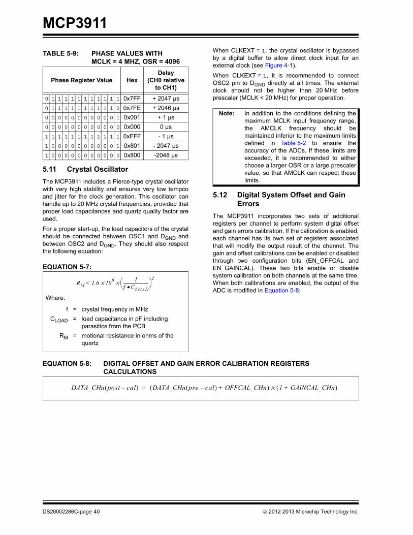
MCP3911
5.11 Crystal Oscillator
The MCP3911 includes a Pierce-type crystal oscillatorwith very high stability and ensures very low tempcoand jitter for the clock generation. This oscillator canhandle up to 20 MHz crystal frequencies, provided thatproper load capacitances and quartz quality factor areused.
For a proper start-up, the load capacitors of the crystalshould be connected between OSC1 and DGND andbetween OSC2 and DGND. They should also respectthe following equation:
EQUATION 5-7:
When CLKEXT = 1, the crystal oscillator is bypassedby a digital buffer to allow direct clock input for anexternal clock (see Figure 4-1).
When CLKEXT = 1, it is recommended to connectOSC2 pin to DGND directly at all times. The externalclock should not be higher than 20 MHz beforeprescaler (MCLK < 20 MHz) for proper operation.
5.12 Digital System Offset and Gain Errors
The MCP3911 incorporates two sets of additionalregisters per channel to perform system digital offsetand gain errors calibration. If the calibration is enabled,each channel has its own set of registers associatedthat will modify the output result of the channel. Thegain and offset calibrations can be enabled or disabledthrough two configuration bits (EN_OFFCAL andEN_GAINCAL). These two bits enable or disablesystem calibration on both channels at the same time.When both calibrations are enabled, the output of theADC is modified in Equation 5-8:
EQUATION 5-8: DIGITAL OFFSET AND GAIN ERROR CALIBRATION REGISTERS CALCULATIONS
TABLE 5-9: PHASE VALUES WITHMCLK = 4 MHZ, OSR = 4096
Phase Register Value HexDelay
(CH0 relativeto CH1)
0 1 1 1 1 1 1 1 1 1 1 1 0x7FF + 2047 µs
0 1 1 1 1 1 1 1 1 1 1 0 0x7FE + 2046 µs
0 0 0 0 0 0 0 0 0 0 0 1 0x001 + 1 µs
0 0 0 0 0 0 0 0 0 0 0 0 0x000 0 µs
1 1 1 1 1 1 1 1 1 1 1 1 0xFFF - 1 µs
1 0 0 0 0 0 0 0 0 0 0 1 0x801 - 2047 µs
1 0 0 0 0 0 0 0 0 0 0 0 0x800 -2048 µs
RM 1.6 106× 1
f C• LOAD------------------------ ×
2<
Where:
f = crystal frequency in MHz
CLOAD = load capacitance in pF including parasitics from the PCB
RM = motional resistance in ohms of the quartz
Note: In addition to the conditions defining themaximum MCLK input frequency range,the AMCLK frequency should bemaintained inferior to the maximum limitsdefined in Table 5-2 to ensure theaccuracy of the ADCs. If these limits areexceeded, it is recommended to eitherchoose a larger OSR or a large prescalervalue, so that AMCLK can respect theselimits.
DATA_CHn post cal–( ) DATA_CHn pre cal–( ) OFFCAL_CHn+( ) 1 GAINCAL_CHn+( )×=
DS20002286C-page 40 2012-2013 Microchip Technology Inc.

MCP3911
5.12.1 DIGITAL OFFSET ERROR CALIBRATION
The OFFCAL_CHn registers are 23-bit plus sign two’scomplement register, which LSB value is the same asthe Channel ADC Data. These two registers are thenadded bit-by-bit to the ADC output codes, if theEN_OFFCAL bit is enabled. Enabling the EN_OFFCALbit does not create any pipeline delay, the offsetaddition is instantaneous. For low OSR values, only thesignificant digits are added to the output (up to theresolution of the ADC. For example, at OSR = 32, onlythe 17 first bits are added).
The offset is not added when the correspondingchannel is in Reset or Shutdown mode. Thecorresponding input voltage offset value added by eachLSB in these 24-bit registers is shown in Equation 5-9.
EQUATION 5-9:
This register is a “Don't Care” if EN_OFFCAL = 0(Offset calibration disabled), but its value is not clearedby the EN_OFFCAL bit.
5.12.2 DIGITAL GAIN ERROR CALIBRATION
This register is 24-bit signed MSB first coding with arange of -1x to +0.9999999x (from 0x80000 to0x7FFFFF). The gain calibration adds 1x to thisregister and multiplies it to the output code of thechannel bit-by-bit, after offset calibration. The range ofthe gain calibration is thus from 0x to 1.9999999x (from0x80000 to 0x7FFFFF). The LSB corresponds to a 2-23
increment in the multiplier.
Enabling EN_GAINCAL creates a pipeline delay of24 DMCLK periods on both channels. All data readypulses are delayed by 24 DMCLK periods, startingfrom the data ready, following the command enablingEN_GAINCAL bit. The gain calibration is effective onthe next data ready, following the command enablingEN_GAINCAL bit.
The digital gain calibration does not function when thecorresponding channel is in Reset or Shutdown mode.The gain multiplier value for an LSB in these 24-bitregisters is shown in Equation 5-10.
EQUATION 5-10:
This register is a “Don't Care” if EN_GAINCAL = 0(Offset calibration disabled), but its value is not clearedby the EN_GAINCAL bit.
If the output result is out of bounds after all calibrationsare performed, the output data on channel is kept toeither 7FFF or 8000 in 16-bit mode or 7FFFFF or 8000in 24-bit mode.
OFFSET(1LSB) = VREF /(PGA_CHn x 1.5 x 8388608)
GAIN (1LSB) = 1/8388608
2012-2013 Microchip Technology Inc. DS20002286C-page 41

MCP3911
NOTES:
DS20002286C-page 42 2012-2013 Microchip Technology Inc.
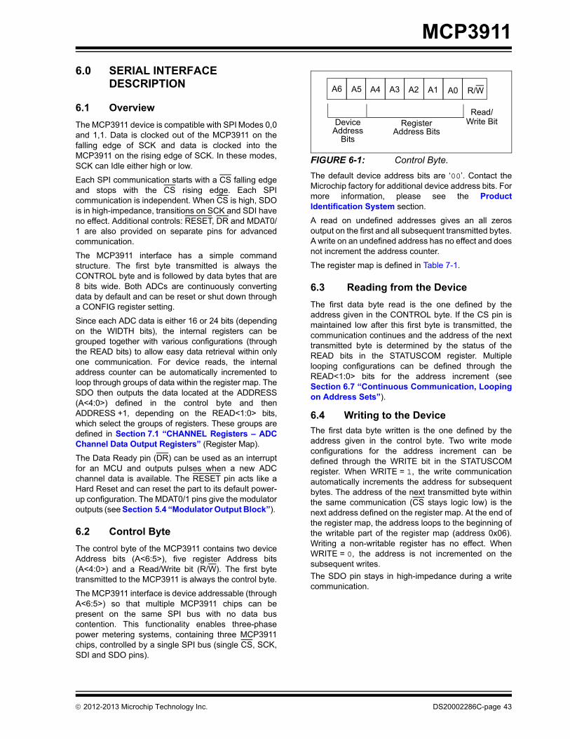
MCP3911
6.0 SERIAL INTERFACE DESCRIPTION
6.1 Overview
The MCP3911 device is compatible with SPI Modes 0,0and 1,1. Data is clocked out of the MCP3911 on thefalling edge of SCK and data is clocked into theMCP3911 on the rising edge of SCK. In these modes,SCK can Idle either high or low.
Each SPI communication starts with a CS falling edgeand stops with the CS rising edge. Each SPIcommunication is independent. When CS is high, SDOis in high-impedance, transitions on SCK and SDI haveno effect. Additional controls: RESET, DR and MDAT0/1 are also provided on separate pins for advancedcommunication.
The MCP3911 interface has a simple commandstructure. The first byte transmitted is always theCONTROL byte and is followed by data bytes that are8 bits wide. Both ADCs are continuously convertingdata by default and can be reset or shut down througha CONFIG register setting.
Since each ADC data is either 16 or 24 bits (dependingon the WIDTH bits), the internal registers can begrouped together with various configurations (throughthe READ bits) to allow easy data retrieval within onlyone communication. For device reads, the internaladdress counter can be automatically incremented toloop through groups of data within the register map. TheSDO then outputs the data located at the ADDRESS(A<4:0>) defined in the control byte and thenADDRESS +1, depending on the READ<1:0> bits,which select the groups of registers. These groups aredefined in Section 7.1 “CHANNEL Registers – ADCChannel Data Output Registers” (Register Map).
The Data Ready pin (DR) can be used as an interruptfor an MCU and outputs pulses when a new ADCchannel data is available. The RESET pin acts like aHard Reset and can reset the part to its default power-up configuration. The MDAT0/1 pins give the modulatoroutputs (see Section 5.4 “Modulator Output Block”).
6.2 Control Byte
The control byte of the MCP3911 contains two deviceAddress bits (A<6:5>), five register Address bits(A<4:0>) and a Read/Write bit (R/W). The first bytetransmitted to the MCP3911 is always the control byte.
The MCP3911 interface is device addressable (throughA<6:5>) so that multiple MCP3911 chips can bepresent on the same SPI bus with no data buscontention. This functionality enables three-phasepower metering systems, containing three MCP3911chips, controlled by a single SPI bus (single CS, SCK,SDI and SDO pins).
FIGURE 6-1: Control Byte.
The default device address bits are ‘00’. Contact theMicrochip factory for additional device address bits. Formore information, please see the ProductIdentification System section.
A read on undefined addresses gives an all zerosoutput on the first and all subsequent transmitted bytes.A write on an undefined address has no effect and doesnot increment the address counter.
The register map is defined in Table 7-1.
6.3 Reading from the Device
The first data byte read is the one defined by theaddress given in the CONTROL byte. If the CS pin ismaintained low after this first byte is transmitted, thecommunication continues and the address of the nexttransmitted byte is determined by the status of theREAD bits in the STATUSCOM register. Multiplelooping configurations can be defined through theREAD<1:0> bits for the address increment (seeSection 6.7 “Continuous Communication, Loopingon Address Sets”).
6.4 Writing to the Device
The first data byte written is the one defined by theaddress given in the control byte. Two write modeconfigurations for the address increment can bedefined through the WRITE bit in the STATUSCOMregister. When WRITE = 1, the write communicationautomatically increments the address for subsequentbytes. The address of the next transmitted byte withinthe same communication (CS stays logic low) is thenext address defined on the register map. At the end ofthe register map, the address loops to the beginning ofthe writable part of the register map (address 0x06).Writing a non-writable register has no effect. WhenWRITE = 0, the address is not incremented on thesubsequent writes.
The SDO pin stays in high-impedance during a writecommunication.
A6 A5 A4 A3 A2 A1 A0 R/W
Read/Write BitRegisterDevice
Address BitsAddressBits
2012-2013 Microchip Technology Inc. DS20002286C-page 43

MCP3911
6.5 SPI MODE 1,1 – Clock Idle High, Read/Write Examples
In this SPI mode, SCK idles high. For the MCP3911,this means that there is a falling edge on SCK beforethere is a rising edge.
:
FIGURE 6-2: Device Read (SPI Mode 1,1 – SCK Idles High).
FIGURE 6-3: Device Write (SPI Mode 1,1 – SCK Idles High).
Note: Changing from an SPI Mode 1,1 to an SPIMode 0,0 is possible and can be donewhile CS pin is logic high.
SCK
SDI
SDO
CS
A6 A5 A4 A3 A2 A1 A0
D6 D5 D4 D3 D2 D1 D0
(ADDRESS) DATA (ADDRESS + 1) DATA
D6 D5 D4 D3 D2 D1
Data Transitions on the Falling Edge
MCU and MCP3911 LatchBits on the Rising Edge
D0HI-Z HI-Z
D7 D7
R/W
HI-Z
SCK
SDI
SDO
CS
R/WA6 A5 A4 A3 A2 A1 A0 D7 D6 D5 D4 D3 D2 D1
(ADDRESS) DATA (ADDRESS + 1) DATA
D6 D5 D4 D3 D2 D1D0
Data Transitions onthe Falling Edge
MCU and MCP3911 LatchBits on the Rising Edge
D0
HI-Z HI-Z
D7
HI-Z
DS20002286C-page 44 2012-2013 Microchip Technology Inc.

MCP3911
6.6 SPI MODE 0,0 – Clock Idle Low, Read/Write Examples
In this SPI mode, SCK idles low. For the MCP3911, thismeans that there is a rising edge on SCK before thereis a falling edge.
FIGURE 6-4: Device Read (SPI Mode 0,0 – SCK Idles Low).
FIGURE 6-5: Device Write (SPI Mode 0,0 – SCK Idles Low).
SCK
SDI
SDO
CS
R/WA6 A5 A4 A3 A2 A1 A0
D7 D6 D5 D4 D3 D2 D1 D0
(ADDRESS) DATA (ADDRESS + 1) DATA
D7 D6 D5 D4 D3 D2 D1
Data Transitions onthe Falling Edge
MCU and MCP3911 LatchBits on the Rising Edge
D0 D7 OF (ADDRESS + 2) DATAHI-Z HI-ZHI-Z
SCK
SDI
SDO
CS
R/WA6 A5 A4 A3 A2 A1 A0 D7 D6 D5 D4 D3 D2 D1 D7
(ADDRESS) DATA (ADDRESS + 1) DATA
D6 D5 D4 D3 D2 D1 D7 OF (ADDRESS + 2) DATAD0
Data Transitions onthe Falling Edge
MCU and MCP3911 LatchBits on the Rising Edge
D0
HI-Z HI-Z
HI-Z
2012-2013 Microchip Technology Inc. DS20002286C-page 45
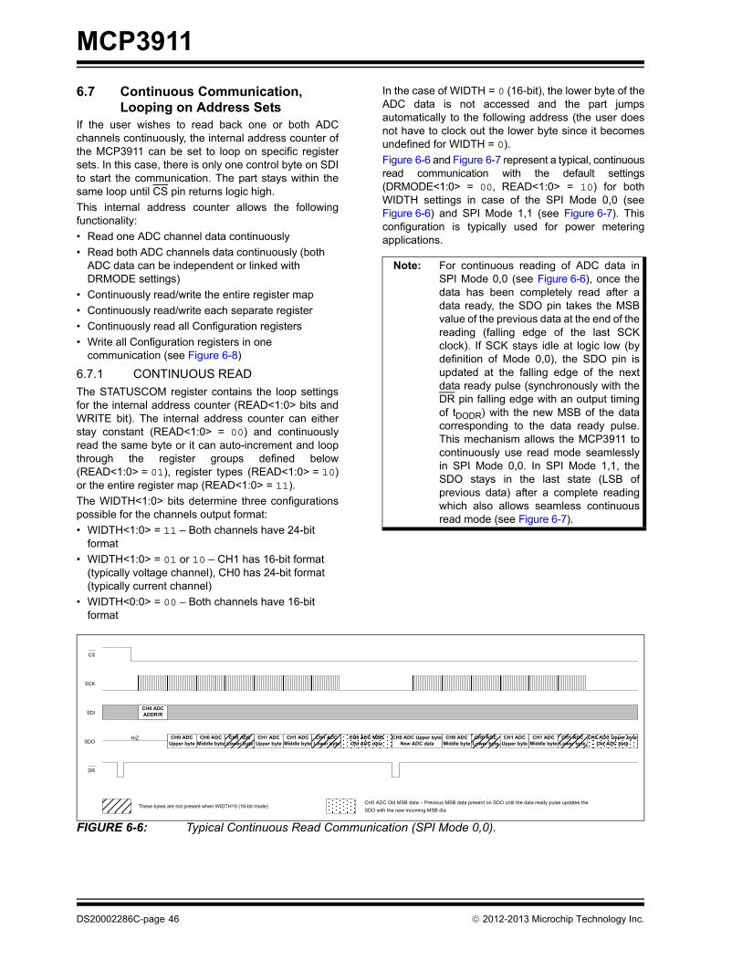
MCP3911
6.7 Continuous Communication, Looping on Address Sets
If the user wishes to read back one or both ADCchannels continuously, the internal address counter ofthe MCP3911 can be set to loop on specific registersets. In this case, there is only one control byte on SDIto start the communication. The part stays within thesame loop until CS pin returns logic high.
This internal address counter allows the followingfunctionality:
• Read one ADC channel data continuously
• Read both ADC channels data continuously (both ADC data can be independent or linked with DRMODE settings)
• Continuously read/write the entire register map
• Continuously read/write each separate register
• Continuously read all Configuration registers
• Write all Configuration registers in one communication (see Figure 6-8)
6.7.1 CONTINUOUS READ
The STATUSCOM register contains the loop settingsfor the internal address counter (READ<1:0> bits andWRITE bit). The internal address counter can eitherstay constant (READ<1:0> = 00) and continuouslyread the same byte or it can auto-increment and loopthrough the register groups defined below(READ<1:0> = 01), register types (READ<1:0> = 10)or the entire register map (READ<1:0> = 11).
The WIDTH<1:0> bits determine three configurationspossible for the channels output format:
• WIDTH<1:0> = 11 – Both channels have 24-bit format
• WIDTH<1:0> = 01 or 10 – CH1 has 16-bit format (typically voltage channel), CH0 has 24-bit format (typically current channel)
• WIDTH<0:0> = 00 – Both channels have 16-bit format
In the case of WIDTH = 0 (16-bit), the lower byte of theADC data is not accessed and the part jumpsautomatically to the following address (the user doesnot have to clock out the lower byte since it becomesundefined for WIDTH = 0).
Figure 6-6 and Figure 6-7 represent a typical, continuousread communication with the default settings(DRMODE<1:0> = 00, READ<1:0> = 10) for bothWIDTH settings in case of the SPI Mode 0,0 (seeFigure 6-6) and SPI Mode 1,1 (see Figure 6-7). Thisconfiguration is typically used for power meteringapplications.
FIGURE 6-6: Typical Continuous Read Communication (SPI Mode 0,0).
Note: For continuous reading of ADC data inSPI Mode 0,0 (see Figure 6-6), once thedata has been completely read after adata ready, the SDO pin takes the MSBvalue of the previous data at the end of thereading (falling edge of the last SCKclock). If SCK stays idle at logic low (bydefinition of Mode 0,0), the SDO pin isupdated at the falling edge of the nextdata ready pulse (synchronously with theDR pin falling edge with an output timingof tDODR) with the new MSB of the datacorresponding to the data ready pulse.This mechanism allows the MCP3911 tocontinuously use read mode seamlesslyin SPI Mode 0,0. In SPI Mode 1,1, theSDO stays in the last state (LSB ofprevious data) after a complete readingwhich also allows seamless continuousread mode (see Figure 6-7).
CH0 ADC ADDR/R
CS
SCK
SDI
CH0 ADC Upper byteSDO
CH0 ADC Middle byte
CH0 ADC Lower byte
DR
CH1 ADC Upper byte
CH1 ADC Middle byte
CH1 ADC Lower byte
CH0 ADC Upper byteNew ADC data
CH0 ADC Middle byte
CH0 ADC Lower byte
CH1 ADC Upper byte
CH1 ADC Middle byte
CH1 ADC Lower byte
These bytes are not present when WIDTH=0 (16-bit mode)
HiZ CH0 ADC MSBOld ADC data
CH0 ADC Upper byteOld ADC data
CH0 ADC Old MSB data – Previous MSB data present on SDO until the data ready pulse updates the SDO with the new incoming MSB dta
DS20002286C-page 46 2012-2013 Microchip Technology Inc.

MCP3911
FIGURE 6-7: Typical Continuous Read Communication (SPI Mode 1,1).
6.7.2 CONTINUOUS WRITE
Both ADCs are powered up with their defaultconfigurations and begin to output data ready pulsesimmediately (RESET<1:0> and SHUTDOWN<1:0>bits are off by default).
The default output codes for both ADCs are all zeros.The default modulator output for both ADCs is ‘0011’(corresponding to a theoretical zero voltage at theinputs). The default phase is zero between the twochannels.
It is recommended to enter into ADC Reset mode forboth ADCs, just after power-up. It is because thedesired MCP3911 register configuration may not be thedefault one. In this case, the ADC outputs undesireddata. Within the ADC Reset mode (RESET<1:0> = 11),the user can configure the whole part with a singlecommunication. The write commands automaticallyincrement the address so that the user can start writingthe PHASE register and finish with the CONFIGregister in only one communication (see Figure 6-8).The RESET<1:0> bits are in the last byte of theCONFIG register to allow exiting the Soft Reset mode,and have the whole part configured and ready to run inonly one command.
6.7.3 REGISTER GROUPS AND TYPES
The following register sets are defined as groups:
The following register sets are defined as types:
6.8 Situations that Reset ADC Data
Immediately after the following actions, the ADCs arereset and automatically restarted to provide properoperation:
1. Change in PHASE register
2. Change in the OSR setting
3. Change in the PRESCALE setting
4. Overwrite of the same PHASE register value
5. Change in the CLKEXT setting
6. Change in the VREFEXT setting
7. Change in the MODOUT setting
After these temporary resets, the ADCs go back tonormal operation without the need for an additionalcommand. If the same value is written in the PHASEregister, it can be used to serially Soft Reset the ADCs,without using the RESET bits in the Configurationregister.
CH0 ADC ADDR/R
CS
SCK
SDI
CH0 ADC Upper byteSDO
CH0 ADC Middle byte
CH0 ADC Lower byte
DR
CH1 ADC Upper byte
CH1 ADC Middle byte CH1 ADC Lower byte CH0 ADC
Upper byteCH0 ADC
Middle byteCH0 ADC
Lower byteCH1 ADC
Upper byteCH1 ADC
Middle byte CH1 ADC Lower byte
These bytes are not present when WIDTH=0 (16-bit mode)
HiZ
TABLE 6-1: REGISTER GROUPS
Group Addresses
ADC DATA CH0 0x00-0x02
ADC DATA CH1 0x03-0x05
MOD, PHASE, GAIN 0x06-0x09
CONFIG, STATUSCOM 0x0A-0x0D
OFFCAL_CH0, GAINCAL_CH0 0x0E-0x13
OFFCAL_CH1, GAINCAL_CH1 0x14-0x19
VREFCAL 0x1A
TABLE 6-2: REGISTER TYPES
Type Addresses
ADC DATA (both channels) 0x00-0x05
CONFIGURATION 0x06-0x1A
2012-2013 Microchip Technology Inc. DS20002286C-page 47

MCP3911
FIGURE 6-8: Recommended Configuration Sequence at Power-up.
6.9 Data Ready Pin (DR)
To signify when channel data is ready for transmission,the data ready signal is available on the Data Ready pin(DR) through an active-low pulse at the end of achannel conversion.
The data ready pin outputs an active-low pulse with aperiod that is equal to the DRCLK period and a widthequal to one DMCLK period.
When not active-low, this pin can either be in high-impedance (when DR_HIZ = 0) or in a defined logichigh state (when DR_HIZ = 1). This is controlledthrough the STATUSCOM register. This allows multipledevices to share the same data ready pin (with apull-up resistor connected between DR and DVDD) in3-phase energy meter designs to reduce pin count. Asingle device on the bus does not require a pull-upresistor and therefore it is recommended to useDR_HIZ = 1 configuration for such applications.
After a data ready pulse has occurred, the ADC outputdata can be read through SPI communication. Two setsof latches at the output of the ADC prevent thecommunication from outputting corrupted data (seeSection 6.10 “ADC Data Latches and Data ReadyModes (DRMODE<1:0>)”).
The CS pin has no effect on the DR pin, which meanseven if CS is logic high, data ready pulses will beprovided (except when the configuration prevents themfrom outputting data ready pulses). The DR pin can beused as an interrupt when connected to an MCU or aDSP. While the RESET pin is logic low, the DR pin isnot active.
6.10 ADC Data Latches and Data Ready Modes (DRMODE<1:0>)
To ensure that both channels’ ADC data is present atthe same time for SPI read, regardless of phase delaysettings for either or both channels, there are two setsof ADC data latches in series with both the data readyand the ‘read start’ triggers.
The first set of latches holds each output when the datais ready and latches both outputs together whenDRMODE<1:0> = 00. When this mode is on, bothADCs work together and produce one set of availabledata after each data ready pulse (that corresponds tothe lagging ADC data ready). The second set of latchesensures that when reading starts on an ADC output, thecorresponding data is latched so that no datacorruption can occur.
If an ADC read has started, to read the following ADCoutput, the current reading needs to be completed (allbits must be read from the ADC Output Data registers).
00011010
CS
SCK
SDI
AVDD, DVDD
11XXXXXX
CONFIG2
ADDR/W
CONFIG2
Optional RESET of both ADCs One command for writing complete configuration (without calibration)
PHASE ADDR/W GAIN STATUSCOM CONFIGPHASE
00001110 xxxxxxxx xxxxxxxx xxxxxxxx xxxxxxxx xxxxxxxx xxxxxxxx xxxxxxxx
DS20002286C-page 48 2012-2013 Microchip Technology Inc.

MCP3911
6.10.1 DATA READY PIN (DR) CONTROL USING DRMODE BITS
There are four modes that control the data readypulses and these modes are set with theDRMODE<1:0> bits in the STATUSCOM register. Forpower metering applications, DRMODE<1:0> = 00 isrecommended (Default mode).
The position of the data ready pulses vary, with respectto this mode, to the OSR and to the PHASE settings:
• DRMODE<1:0> = 11: Both data ready pulsesfrom ADC Channel 0 and ADC Channel 1 areoutput on the DR pin.
• DRMODE<1:0> = 10: Data ready pulses fromADC Channel 1 are output on the DR pin. Thedata ready pulse from ADC Channel 0 is notpresent on the pin.
• DRMODE<1:0> = 01: Data ready pulses fromADC Channel 0 are output on the DR pin. Thedata ready pulse from ADC Channel 1 is notpresent on the pin.
• DRMODE<1:0> = 00 (Recommended andDefault mode): Data ready pulses from thelagging ADC between the two are output on theDR pin. The lagging ADC depends on the PHASEregister and on the OSR. In this mode, the twoADCs are linked so their data is latched togetherwhen the lagging ADC output is ready.
6.10.2 ADC CHANNELS LATCHING AND SYNCHRONIZATION
The ADC channels data output registers (addresses0x00 to 0x05) have a double buffer output structure.The two sets of latches in series are triggered by thedata ready signal and an internal signal indicating thebeginning of a read communication sequence (readstart).
The first set of latches holds each ADC channel dataoutput register when the data is ready and latches bothoutputs together when DRMODE<1:0> = 00. Thisbehavior is synchronous with the MCLK.
The second set of latches ensures that when readingstarts on an ADC output, the corresponding data islatched so that no data corruption can occur within aread. This behavior is synchronous with the SCK clock.If an ADC read has started, to read the following ADCoutput, the current reading needs to be fully completed(all bits must be read on the SDO pin from the ADCoutput data registers).
Since the double output buffer structure is triggeredwith two events that depend on two asynchronousclocks (data ready with MCLK and read start with SCK),it is recommended to synchronize the reading of thechannels with the MCU or processor using one of thefollowing methods:
1. Use the data ready pin pulses as an interrupt– Once a falling edge occurs on the DR pin, thedata is available for reading on the ADC outputregisters after the tDODR timing. If this timing isnot respected, data corruption can occur.
2. Use a timer clocked with MCLK as asynchronization event – Since the data readyis synchronous with MCLK, the user cancalculate the position of the data readydepending on the PHASE<11:0>, theOSR<2:0> and the PRE<1:0> settings for eachchannel. Here, the tDODR timing needs to beadded to this calculation to avoid datacorruption.
3. Poll the DRSTATUS<1:0> bits in theSTATUSCOM register – This method consistsof reading continuously the STATUSCOMregister and waits for the DRSTATUS bits to beequal to ‘0’. When this event happens, the usercan start a new communication to read thedesired ADC data. In this case, no additionaltiming is required.
The first method is the preferred method as it can beused without adding additional MCU code space, but itrequires connecting the DR pin to an I/O pin of themicrocontroller. The other two methods require moreMCU code space and execution time, but they allowsynchronizing the reading of the channels withoutconnecting the DR pin, which saves one I/O pin on theMCU.
6.10.3 DATA READY PULSES WITH SHUTDOWN OR RESET CONDITIONS
There are no data ready pulses if DRMODE<1:0> = 00when either one or both of the ADCs are in Reset orShutdown mode. In Mode 0,0, a data ready pulse onlyhappens when both ADCs are ready. Any data readypulse corresponds to one data on both ADCs. The twoADCs are linked together and act as if there was onlyone channel with the combined data of both ADCs.This mode is very practical when both ADC channels’data retrieval and processing need to be synchronized,as in power metering applications.
Note: If DRMODE<1:0> = 11, the user is stillable to retrieve the data ready pulse forthe ADC not in Shutdown or Reset mode(i.e., only 1 ADC channel needs to beawake).
2012-2013 Microchip Technology Inc. DS20002286C-page 49

MCP3911
Figure 6-9 represents the behavior of the data readypin with the different DRMODE configurations whileshutdown or reset is applied.
DS20002286C-page 50 2012-2013 Microchip Technology Inc.

MC
P3911
DS
20002286C
-page 51
2012-2013 M
icrochip Technolo
gy Inc.
D16 D17 D18 D19
D13 D14 D15 D16
D13 D15 D16D14
D10 D11 D12 D13
D11
D13 D14 D15 D16
D12 D13 D14
D14
D28 D29 D31 D33D27 D30 D32 D34
D15 D16 D17
D13
D11 D12 D13 D14
D28 D29 D31 D33D27 D30 D32 D34
D14 D15 D16
D15 D16 D17
DRCLK periodInternal reset synchronisation
(1 DMCLK period)
3*DRCLK period
D14
FIGURE 6-9: Data Ready Behavior.
D0 D1 D2
D0 D1 D2 D3 D4 D5
D3 D4 D5
D0 D1 D2 D3 D4 D5 D6 D7 D8
D1 D3 D5 D6 D7 D8 D10 D12D0 D2 D4 D9 D11 D13 D14
D6
D6 D12
D9 D13
D16 D17 D18 D19 D21 D24D15 D20 D22 D25 D26
D7 D8 D9 D10 D11
D10 D11 D12
D10D7 D8 D9
D23
D0 D1 D2 D3 D4 D5 D6 D7 D8 D9 D10 D11 D12 D13 D14 D15
D0 D1 D2 D3 D4 D5 D6 D7 D8 D9 D11D10 D12
D0 D1 D2 D4 D5D3 D7 D8 D9 D10 D11 D12D6
D0 D1 D2 D6 D8D7 D9D4 D5D3
RESET<1> or
SHUTDOWN<1>
RESET<0> or
SHUTDOWN<0>
RESET
D0 D1 D2 D3 D4 D5
D0 D1 D2 D3 D4 D5 D6 D7 D8
D1 D3 D5 D6 D7 D8 D11 D13D0 D2 D4 D10 D12 D14 D15
D6
D9
D17 D18 D21 D24D16 D19 D22 D25 D26
D10 D11 D12
D10D8 D9
D23
D0 D1 D2 D3 D4 D5 D12D11 D13D8 D9 D10
D7
PH
AS
E <
0
PH
AS
E =
0
P
HA
SE
> 0
D6 D7
DRCLK Period
3*DRCLK period
D9 D20
DRMODE=00; DR
DRMODE=01; DR
DRMODE=10; DR
DRMODE=11; DR
DRMODE=00; DR
DRMODE=01; DR
DRMODE=10; DR
DRMODE=11; DR
DRMODE=00; DR
DRMODE=01; DR
DRMODE=10; DR
DRMODE=11; DR
DRMODE = 00: Select the lagging Data Ready
DRMODE = 01: Select the Data Ready on Channel 0
DRMODE = 10: Select the Data Ready on Channel 1
DRMODE = 11: Select both Data ready
DRCLK Period1 DMCLK Period
Internal data ready pulse (filtered because it corresponds to unsettled data)

MCP3911
NOTES:
DS20002286C-page 52 2012-2013 Microchip Technology Inc.

MCP3911
7.0 INTERNAL REGISTERS
The addresses associated with the internal registersare listed below, followed by a detailed description ofthe registers. All registers are split in 8-bit long registerswhich can be addressed and read separately. Readand Write modes define the groups and types ofregisters for continuous read/write communication orlooping on address sets as shown in Table 7-2.
TABLE 7-1: REGISTER MAP
Address Name Bits R/W Description
0x00 CHANNEL0 24 R Channel 0 ADC 24-bit Data <23:0>, MSB first
0x03 CHANNEL1 24 R Channel 1 ADC 24-bit Data <23:0>, MSB first
0x06 MOD 8 R/W Modulator Output Register for both ADC channels
0x07 PHASE 16 R/W Phase Delay Configuration Register
0x09 GAIN 8 R/W Gain and Boost Configuration Register
0x0A STATUSCOM 16 R/W Status and Communication Register
0x0C CONFIG 16 R/W Configuration Register
0x0E OFFCAL_CH0 24 R/W Offset Correction Register - Channel 0
0x11 GAINCAL_CH0 24 R/W Gain Correction Register - Channel 0
0x14 OFFCAL_CH1 24 R/W Offset Correction Register - Channel 1
0x17 GAINCAL_CH1 24 R/W Gain Correction Register - Channel 1
0x1A VREFCAL 8 R/W Internal Voltage reference Temperature Coefficient Adjustment Register
2012-2013 Microchip Technology Inc. DS20002286C-page 53
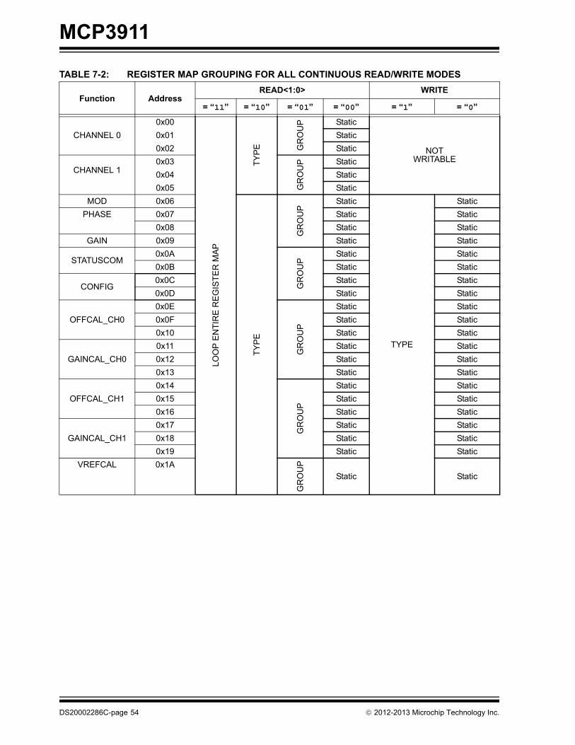
MCP3911
.
TABLE 7-2: REGISTER MAP GROUPING FOR ALL CONTINUOUS READ/WRITE MODES
Function AddressREAD<1:0> WRITE
= “11” = “10” = “01” = “00” = “1” = “0”
CHANNEL 0
0x00
LOO
P E
NT
IRE
RE
GIS
TE
R M
AP
TY
PE G
RO
UP Static
NOTWRITABLE
0x01 Static
0x02 Static
CHANNEL 10x03
GR
OU
P Static
0x04 Static
0x05 Static
MOD 0x06
TY
PE
GR
OU
P
Static
TYPE
Static
PHASE 0x07 Static Static
0x08 Static Static
GAIN 0x09 Static Static
STATUSCOM0x0A
GR
OU
P
Static Static
0x0B Static Static
CONFIG0x0C Static Static
0x0D Static Static
OFFCAL_CH0
0x0EG
RO
UP
Static Static
0x0F Static Static
0x10 Static Static
GAINCAL_CH0
0x11 Static Static
0x12 Static Static
0x13 Static Static
OFFCAL_CH1
0x14
GR
OU
P
Static Static
0x15 Static Static
0x16 Static Static
GAINCAL_CH1
0x17 Static Static
0x18 Static Static
0x19 Static Static
VREFCAL 0x1A
GR
OU
P
Static Static
DS20002286C-page 54 2012-2013 Microchip Technology Inc.

MCP3911
7.1 CHANNEL Registers – ADC Channel Data Output Registers
The ADC Channel Data Output registers alwayscontain the most recent A/D conversion data for eachchannel. These registers are read-only and can beaccessed independently or linked together (withREAD<1:0> bits). These registers are latched when anADC read communication occurs. When a data readyevent occurs during a read communication, the most
current ADC data is also latched to avoid datacorruption issues. The three bytes of each channel areupdated synchronously at a DRCLK rate. The threebytes can be accessed separately if needed but arerefreshed synchronously.
Name Bits Address R/W
CHANNEL0 24 0x00 R
CHANNEL1 24 0x03 R
REGISTER 7-1: CHANNEL REGISTER
R-0 R-0 R-0 R-0 R-0 R-0 R-0 R-0
DATA_CHn<23> (MSB)
DATA_CHn<22>
DATA_CHn<21>
DATA_CHn<20>
DATA_CHn<19>
DATA_CHn<18>
DATA_CHn<17>
DATA_CHn<16>
bit 23 bit 16
R-0 R-0 R-0 R-0 R-0 R-0 R-0 R-0
DATA_CHn<15>
DATA_CHn<14>
DATA_CHn<13>
DATA_CHn<12>
DATA_CHn<11>
DATA_CHn<10>
DATA_CHn<9>
DATA_CHn<8>
bit 15 bit 8
R-0 R-0 R-0 R-0 R-0 R-0 R-0 R-0
DATA_CHn<7>
DATA_CHn<6>
DATA_CHn<5>
DATA_CHn<4>
DATA_CHn<3>
DATA_CHn<2>
DATA_CHn<1>
DATA_CHn<0>
bit 7 bit 0
Legend:
R = Readable bit W = Writable bit U = Unimplemented bit, read as ‘0’
-n = Value at POR ‘1’ = Bit is set ‘0’ = Bit is cleared x = Bit is unknown
bit 23-0 DATA_CHn: Output code from ADC Channel n. This data is post-calibration if the EN_OFFCAL orEN_GAINCAL bits are enabled.
2012-2013 Microchip Technology Inc. DS20002286C-page 55
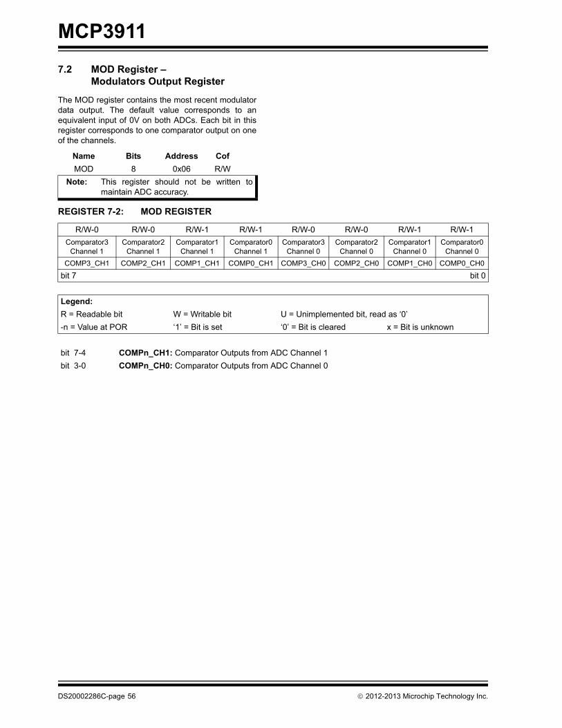
MCP3911
7.2 MOD Register – Modulators Output Register
The MOD register contains the most recent modulatordata output. The default value corresponds to anequivalent input of 0V on both ADCs. Each bit in thisregister corresponds to one comparator output on oneof the channels.
Name Bits Address Cof
MOD 8 0x06 R/W
Note: This register should not be written tomaintain ADC accuracy.
REGISTER 7-2: MOD REGISTER
R/W-0 R/W-0 R/W-1 R/W-1 R/W-0 R/W-0 R/W-1 R/W-1
Comparator3Channel 1
Comparator2Channel 1
Comparator1Channel 1
Comparator0Channel 1
Comparator3Channel 0
Comparator2Channel 0
Comparator1Channel 0
Comparator0Channel 0
COMP3_CH1 COMP2_CH1 COMP1_CH1 COMP0_CH1 COMP3_CH0 COMP2_CH0 COMP1_CH0 COMP0_CH0
bit 7 bit 0
Legend:
R = Readable bit W = Writable bit U = Unimplemented bit, read as ‘0’
-n = Value at POR ‘1’ = Bit is set ‘0’ = Bit is cleared x = Bit is unknown
bit 7-4 COMPn_CH1: Comparator Outputs from ADC Channel 1
bit 3-0 COMPn_CH0: Comparator Outputs from ADC Channel 0
DS20002286C-page 56 2012-2013 Microchip Technology Inc.

MCP3911
7.3 PHASE Register – Phase Configuration Register
Any write to one of these two addresses (0x07 and0x08) creates an internal reset and restart sequence.
Name Bits Address Cof
PHASE 16 0x07 R/W
REGISTER 7-3: PHASE REGISTER
U-0 U-0 U-0 U-0 R/W-0 R/W-0 R/W-0 R/W-0
— — — — PHASE<11> PHASE<10> PHASE<9> PHASE<8>
bit 15 bit 8
R/W-0 R/W-0 R/W-0 R/W-0 R/W-0 R/W-0 R/W-0 R/W-0
PHASE<7> PHASE<6> PHASE<5> PHASE<4> PHASE<3> PHASE<2> PHASE<1> PHASE<0>
bit 7 bit 0
Legend:
R = Readable bit W = Writable bit U = Unimplemented bit, read as ‘0’
-n = Value at POR ‘1’ = Bit is set ‘0’ = Bit is cleared x = Bit is unknown
bit 15-12 Unimplemented: Read as ‘0’
bit 11-0 CH0 relative to CH1 Phase Delay:
PHASE<11:0>: CH0 Relative to CH1 Phase Delay bits. Delay = PHASE Register’s two’s complement code/DMCLK (Default PHASE = 0).
2012-2013 Microchip Technology Inc. DS20002286C-page 57

MCP3911
7.4 GAIN – Gain and Boost Configuration Register
Name Bits Address Cof
GAIN 8 0x09 R/W
REGISTER 7-4: GAIN REGISTER
R/W-1 R/W-0 R/W-0 R/W-0 R/W-0 R/W-0 R/W-0 R/W-0
BOOST<1> BOOST<0> PGA_CH1<2> PGA_CH1<1> PGA_CH1<0> PGA_CH0<2> PGA_CH0<1> PGA_CH0<0>
bit 15 bit 8
Legend:
R = Readable bit W = Writable bit U = Unimplemented bit, read as ‘0’
-n = Value at POR ‘1’ = Bit is set ‘0’ = Bit is cleared x = Bit is unknown
bit 7-6 BOOST<1:0>: Bias Current Selection
11 = Both channels have current x 210 = Both channels have current x 1(DEFAULT)01 = Both channels have current x 0.6600 = Both channels have current x 0.5
bit 5-3 PGA_CH1<2:0>: PGA Setting for Channel 1
111 = Reserved (Gain = 1)110 = Reserved (Gain = 1)101 = Gain is 32100 = Gain is 16011 = Gain is 8010 = Gain is 4001 = Gain is 2000 = Gain is 1 (DEFAULT)
bit 2-0 PGA_CH0<2:0>: PGA Setting for Channel 0
111 = Reserved (Gain = 1)110 = Reserved (Gain = 1)101 = Gain is 32100 = Gain is 16011 = Gain is 8010 = Gain is 4001 = Gain is 2000 = Gain is 1 (DEFAULT)
DS20002286C-page 58 2012-2013 Microchip Technology Inc.
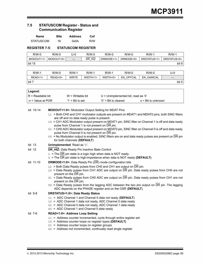
MCP3911
7.5 STATUSCOM Register - Status and Communication Register
Name Bits Address Cof
STATUSCOM 16 0x0A R/W
REGISTER 7-5: STATUSCOM REGISTER
R/W-0 R/W-0 U-0 R/W-0 R/W-0 R/W-0 R/W-1 R/W-1
MODOUT<1> MODOUT<0> — DR_HIZ DRMODE<1> DRMODE<0> DRSTATUS<1> DRSTATUS<0>
bit 15 bit 8
R/W-1 R/W-0 R/W-1 R/W-1 R/W-1 R/W-0 R/W-0 U-0
READ<1> READ<0> WRITE WIDTH<1> WIDTH<0> EN_OFFCAL EN_GAINCAL —
bit 7 bit 0
Legend:
R = Readable bit W = Writable bit U = Unimplemented bit, read as ‘0’
-n = Value at POR ‘1’ = Bit is set ‘0’ = Bit is cleared x = Bit is unknown
bit 15-14 MODOUT<1:0>: Modulator Output Setting for MDAT Pins
11 = Both CH0 and CH1 modulator outputs are present on MDAT1 and MDAT0 pins, both SINC filtersare off and no data ready pulse is present.
10 = CH1 ADC Modulator output present on MDAT1 pin, SINC filter on Channel 1 is off and data readypulse from Channel 1 is not present on DR pin.
01 = CH0 ADC Modulator output present on MDAT0 pin, SINC filter on Channel 0 is off and data readypulse from Channel 0 is not present on DR pin.
00 = No Modulator output is enabled, SINC filters are on and data ready pulses are present on DR pinfor both channels (DEFAULT)
bit 13 Unimplemented: Read as ‘0’.
bit 12 DR_HIZ: Data Ready Pin Inactive State Control
1 = The DR pin state is a logic high when data is NOT ready0 = The DR pin state is high-impedance when data is NOT ready (DEFAULT)
bit 11-10 DRMODE<1:0>: Data Ready Pin (DR) mode configuration bits
11 = Both Data Ready pulses from CH0 and CH1 are output on DR pin.10 = Data Ready pulses from CH1 ADC are output on DR pin. Data ready pulses from CH0 are not
present on the DR pin.01 = Data Ready pulses from CH0 ADC are output on DR pin. Data ready pulses from CH1 are not
present on the DR pin.00 = Data Ready pulses from the lagging ADC between the two are output on DR pin. The lagging
ADC depends on the PHASE register and on the OSR (DEFAULT).
bit 9-8 DRSTATUS<1:0>: Data Ready Status
11 = ADC Channel 1 and Channel 0 data not ready (DEFAULT)10 = ADC Channel 1 data not ready, ADC Channel 0 data ready01 = ADC Channel 0 data not ready, ADC Channel 1 data ready00 = ADC Channel 1 and Channel 0 data ready
bit 7-6 READ<1:0>: Address Loop Setting
11 = Address counter incremented, cycle through entire register set10 = Address counter loops on register types (DEFAULT)01 = Address counter loops on register groups00 = Address not incremented, continually read single register
2012-2013 Microchip Technology Inc. DS20002286C-page 59
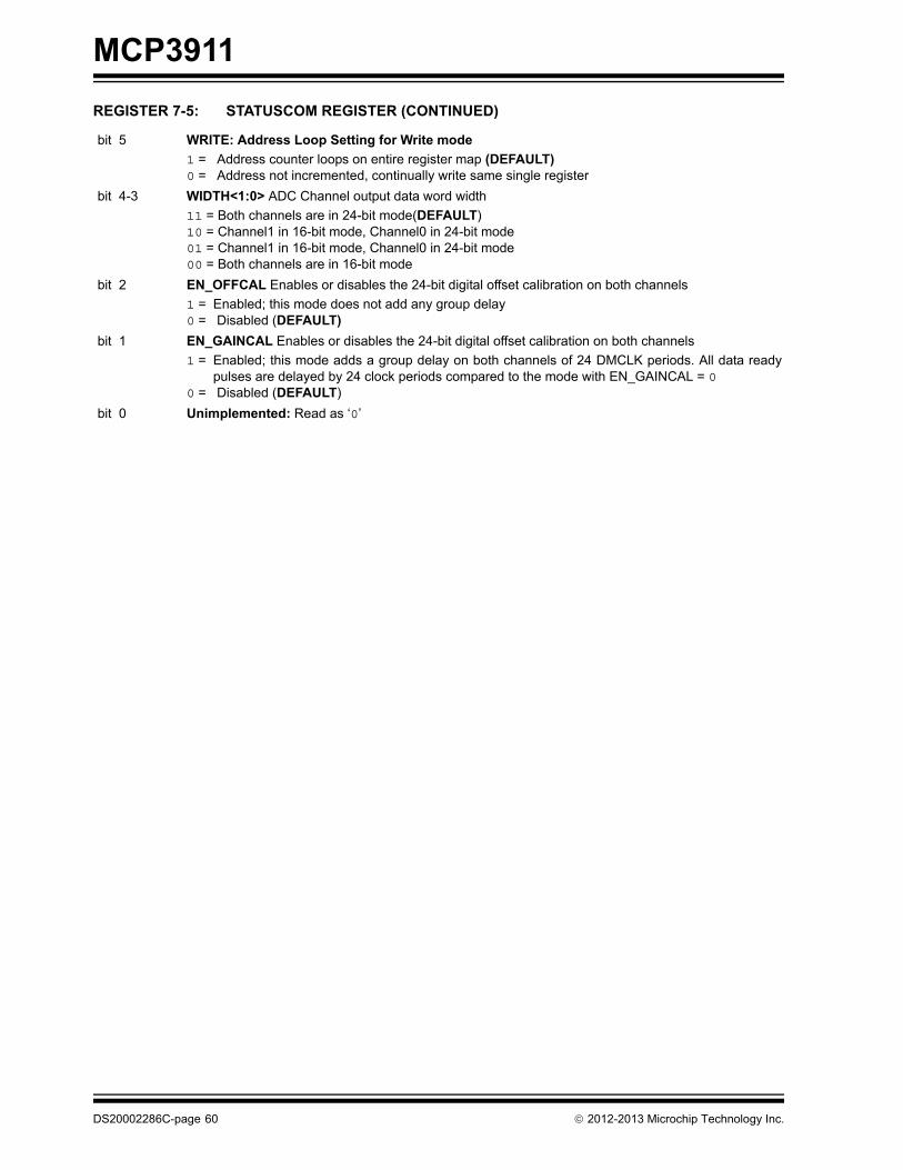
MCP3911
bit 5 WRITE: Address Loop Setting for Write mode
1 = Address counter loops on entire register map (DEFAULT)0 = Address not incremented, continually write same single register
bit 4-3 WIDTH<1:0> ADC Channel output data word width
11 = Both channels are in 24-bit mode(DEFAULT)10 = Channel1 in 16-bit mode, Channel0 in 24-bit mode01 = Channel1 in 16-bit mode, Channel0 in 24-bit mode00 = Both channels are in 16-bit mode
bit 2 EN_OFFCAL Enables or disables the 24-bit digital offset calibration on both channels
1 = Enabled; this mode does not add any group delay0 = Disabled (DEFAULT)
bit 1 EN_GAINCAL Enables or disables the 24-bit digital offset calibration on both channels
1 = Enabled; this mode adds a group delay on both channels of 24 DMCLK periods. All data readypulses are delayed by 24 clock periods compared to the mode with EN_GAINCAL = 0
0 = Disabled (DEFAULT)
bit 0 Unimplemented: Read as ‘0’
REGISTER 7-5: STATUSCOM REGISTER (CONTINUED)
DS20002286C-page 60 2012-2013 Microchip Technology Inc.

MCP3911
7.6 CONFIG Register – Configuration Register
Name Bits Address Cof
CONFIG 16 0x0C R/W
REGISTER 7-6: CONFIG REGISTER
R/W-0 R/W-0 R/W-0 R/W-1 R/W-1 R/W-1 R/W-1 R/W-0
PRE<1> PRE<0> OSR<2> OSR<1> OSR<0> DITHER<1> DITHER<0> AZ_FREQ
bit 15 bit 8
R/W-0 R/W-0 R/W-0 R/W-0 U-0 R/W-0 R/W-1 U-0
RESET<1> RESET<0> SHUT-DOWN<1>
SHUT-DOWN<0>
— VREFEXT CLKEXT —
bit 7 bit 0
Legend:
R = Readable bit W = Writable bit U = Unimplemented bit, read as ‘0’
-n = Value at POR ‘1’ = Bit is set ‘0’ = Bit is cleared x = Bit is unknown
bit 15-14 PRE<1:0>: Analog Master Clock (AMCLK) Prescaler Value
11 = AMCLK = MCLK/810 = AMCLK = MCLK/401 = AMCLK = MCLK/200 = AMCLK = MCLK (DEFAULT)
bit 13-11 OSR<2:0>: Oversampling Ratio for Delta-Sigma A/D Conversion (ALL CHANNELS, fd/fS)
111 = 4096 (fd = 244 sps for MCLK = 4 MHz, fs = AMCLK = 1 MHz)110 = 2048 (fd = 488 sps for MCLK = 4 MHz, fs = AMCLK = 1 MHz)101 = 1024 (fd = 976 sps for MCLK = 4 MHz, fs = AMCLK = 1 MHz)100 = 512 (fd = 1.953 ksps for MCLK = 4 MHz, fs = AMCLK = 1 MHz)011 = 256 (fd = 3.90625 ksps for MCLK = 4 MHz, fs = AMCLK = 1 MHz) (DEFAULT)010 = 128 (fd = 7.8125 ksps for MCLK = 4 MHz, fs = AMCLK = 1 MHz)001 = 64 (fd = 15.625 ksps for MCLK = 4 MHz, fs = AMCLK = 1 MHz)000 = 32 (fd = 31.25 ksps for MCLK = 4 MHz, fs = AMCLK = 1 MHz)
bit 10-9 DITHER<1:0>: Control for dithering circuit for idle tones cancellation and improved THD
11 = Dithering ON, both channels, Strength = Maximum(MCP3901 Equivalent) - (DEFAULT)10 = Dithering ON, both channels, Strength = Medium01 = Dithering ON, both channels, Strength = Minimum00 = Dithering turned OFF
bit 8 AZ_FREQ: Auto-zero frequency setting
1 = Auto-zeroing algorithm running at higher speed0 = Auto-zeroing algorithm running at lower speed (Default)
bit 7-6 RESET<1:0>: Reset mode setting for ADCs
11 = Both CH0 and CH1 ADC are in reset mode10 = CH1 ADC in Reset mode01 = CH0 ADC in Reset mode00 = Neither ADC in Reset mode (default)
bit 5-4 SHUTDOWN<1:0>: Shutdown mode setting for ADCs
11 = Both CH0 and CH1 ADC in Shutdown10 = CH1 ADC in Shutdown01 = CH0 ADC in Shutdown00 = Neither Channel in Shutdown (default)
2012-2013 Microchip Technology Inc. DS20002286C-page 61

MCP3911
7.7 OFFCAL_CHn Registers - Digital Offset Error Calibration Registers
bit 3 Not implemented: Read as ‘0’.
bit 2 VREFEXT Internal Voltage Reference Shutdown Control
1 = Internal Voltage Reference Disabled0 = Internal Voltage Reference Enabled (Default)
bit 1 CLKEXT Internal Clock selection bits
1 = External clock drive by MCU on OSC1 pin (crystal oscillator disabled, no internal powerconsumption) (Default)
0 = Crystal oscillator is enabled. A crystal must be placed between OSC1 and OSC2 pins.
bit 0 Not implemented: Read as ‘0’.
REGISTER 7-6: CONFIG REGISTER (CONTINUED)
Name Bits Address Cof
OFFCAL_CH0 24 0x0E R/W
OFFCAL_CH1 24 0x14 R/W
REGISTER 7-7: OFFCAL_CHn REGISTER
R/W-0 R/W-0 R/W-0 ... R/W-0 R/W-0 R/W-0 R/W-0
OFFCAL_CHn<23>
OFF-CAL_CHn<22>
OFF-CAL_CHn<21>
... OFF-CAL_CHn<3>
OFF-CAL_CHn<2>
OFF-CAL_CHn<1>
OFF-CAL_CHn<0>
bit 23 bit 0
Legend:
R = Readable bit W = Writable bit U = Unimplemented bit, read as ‘0’
-n = Value at POR ‘1’ = Bit is set ‘0’ = Bit is cleared x = Bit is unknown
bit 23-0 Digital Offset calibration value for the corresponding Channel CHn. This register simply is added tothe output code of the channel bit-by-bit. This register is 24-bit two's complement MSB first coding.CHn Output Code = OFFCAL_CHn + ADC CHn Output Code. This register is a “Don't Care” ifEN_OFFCAL = 0 (Offset calibration disabled), but its value is not cleared by the EN_OFFCAL bit.
DS20002286C-page 62 2012-2013 Microchip Technology Inc.

MCP3911
7.8 GAINCAL_CHn Registers - Digital Gain Error Calibration Registers
7.9 VREFCAL Register – Internal Voltage Reference Temperature Coefficient Adjustment Register
This register is only for advanced users. This registershould not be written unless the user wants to calibratethe temperature coefficient of the whole system orapplication. The default value of this register is set to0x42.
Name Bits Address Cof
GAINCAL_CH0 24 0x11 R/W
GAINCAL_CH1 24 0x17 R/W
REGISTER 7-8: GAINCAL_CHn REGISTER
R/W-0 R/W-0 R/W-0 ... R/W-0 R/W-0 R/W-0 R/W-0
GAIN-CAL_CHn<23>
GAIN-CAL_CHn<22>
GAIN-CAL_CHn<21>
... GAIN-CAL_CHn<3>
GAIN-CAL_CHn<2>
GAIN-CAL_CHn<1>
GAIN-CAL_CHn<0>
bit 23 bit 0
Legend:
R = Readable bit W = Writable bit U = Unimplemented bit, read as ‘0’
-n = Value at POR ‘1’ = Bit is set ‘0’ = Bit is cleared x = Bit is unknown
bit 23-0 Digital gain error calibration value for the corresponding Channel CHn. This register is 24-bit signedMSB first coding with a range of -1x to +0.9999999x (from 0x80000 to 0x7FFFFF). The gain calibrationadds 1x to this register and multiplies it to the output code of the channel bit by bit, after the offsetcalibration. Thus, the range of the gain calibration is from 0x to 1.9999999x (from 0x80000 to0x7FFFFF). The LSB corresponds to a 2-23 increment in the multiplier.
CHn Output Code = (GAINCAL_CHn+1) x ADC CHn Output Code. This register is a “Don't Care” ifEN_GAINCAL = 0 (Offset calibration disabled), but its value is not cleared by the EN_GAINCAL bit.
Name Bits Address Cof
VREFCAL 8 0x1A R/W
REGISTER 7-9: VREFCAL REGISTER
R/W-0 R/W-1 R/W-0 R/W-0 R/W-0 R/W-0 R/W-1 R/W-0
VREFCAL<7> VREFCAL<6> VREFCAL<5> VREFCAL<4> VREFCAL<3> VREFCAL<2> VREFCAL<1> VREFCAL<0>
bit 7 bit 0
Legend:
R = Readable bit W = Writable bit U = Unimplemented bit, read as ‘0’
-n = Value at POR ‘1’ = Bit is set ‘0’ = Bit is cleared x = Bit is unknown
bit 7-0 Internal Voltage Temperature coefficient register value (see Section 5.7.3 “Temperaturecompensation (VREFCAL register)” for complete description).
2012-2013 Microchip Technology Inc. DS20002286C-page 63

MCP3911
NOTES:
DS20002286C-page 64 2012-2013 Microchip Technology Inc.

MCP3911
8.0 PACKAGING INFORMATION
8.1 Package Marking Information
20-Lead QFN (4x4x0.9 mm) Example:
20-Lead SSOP Example:
PIN 1 PIN 1
E/ML^^316256
3911A03e
MCP3911A0E/SS^^
13162563e
Legend: XX...X Customer-specific informationY Year code (last digit of calendar year)YY Year code (last 2 digits of calendar year)WW Week code (week of January 1 is week ‘01’)NNN Alphanumeric traceability code Pb-free Compliant JEDEC designator for Matte Tin (Sn)* This package is Pb-free Compliant. The Pb-free Compliant JEDEC designator ( )
can be found on the outer packaging for this package.
Note: In the event the full Microchip part number cannot be marked on one line, it will be carried overto the next line, thus limiting the number of available characters for customer-specificinformation.
3e
3e
2012-2013 Microchip Technology Inc. DS20002286C-page 65

MCP3911
���������� ��������� ������������������������� !��"#���$
�� ��%�� �������� !�����"�#�$��%!��&������'�(!%�&! %�(�����%�"�)�%����%�����%���"������� ���*����� � �)� ���!��%�"�+� ��&�� ��������"�%���������������,�-���.��
/�01 /� �����&�� ���� ���%��������#��%����!�� �)��)�%�!%�%������ ��,21 ��$��������&�� ��'�! !�����)�%�!%�%������'�$���$&�%����!� � �����
�� �% 2�%���& %��!��%����*����"�)��� '����� �� ���%��������������*�����������$���%������%�"��%��%%�133)))�&��������&3���*�����
4��% ��55��, ,����&�� ���5�&�% ��6 67� ��8
6!&(��$���� 6 ����%�� � ��.��/�07������9����% � ��:� ���� �����%��"$$� �� ���� ���� ���.0�%��%� ���*�� �+ ������,27������;�"%� , �����/�0,#� �"���"�;�"%� ,� ��<� ���� ��:�7������5���%� � �����/�0,#� �"���"�5���%� �� ��<� ���� ��:�0�%��%�;�"%� ( ���: ���. ��+�0�%��%�5���%� 5 ��+� ���� ��.�0�%��%�%�,#� �"���" = ���� > >
DEXPOSED
PAD
E
E2
2
1
N
TOP VIEW NOTE 1
N
L
K
b
e
D2
2
1
A
A1A3
BOTTOM VIEW
������� ������� ��)��� 0�����</
DS20002286C-page 66 2012-2013 Microchip Technology Inc.

MCP3911
�� �% 2�%���& %��!��%����*����"�)��� '����� �� ���%��������������*�����������$���%������%�"��%��%%�133)))�&��������&3���*�����
2012-2013 Microchip Technology Inc. DS20002286C-page 67

MCP3911
���������� ��&'(�)�& ���*� ��)��&&��+�,� !��"#&&*$
�� ��%�� �������� !�����"�#�$��%!��&������'�(!%�&! %�(�����%�"�)�%����%�����%���"������� ��&�� �� �����"�,��"��%�����!"��&�"�$�� ����%! �� ����"�$�� ����%! �� � ������%��#���"������&&���� �"��+� ��&�� ��������"�%���������������,�-���.��
/�01 /� �����&�� ���� ���%��������#��%����!�� �)��)�%�!%�%������ ��,21 ��$��������&�� ��'�! !�����)�%�!%�%������'�$���$&�%����!� � �����
�� �% 2�%���& %��!��%����*����"�)��� '����� �� ���%��������������*�����������$���%������%�"��%��%%�133)))�&��������&3���*�����
4��% ��55��, ,����&�� ���5�&�% ��6 67� ��8
6!&(��$���� 6 ����%�� � ��<.�/�07������9����% � > > ������"�"����*���� ���*�� �� ��<. ���. ��:.�%��"$$� �� ���. > >7������;�"%� , ���� ��:� :�����"�"����*����;�"%� ,� .��� .�+� .�<�7������5���%� � <��� ���� ��.�2%�5���%� 5 ��.. ���. ���.2%���% 5� ���.��,25��"� ���*�� � ���� > ���.2%������ � �? �? :?5��"�;�"%� ( ���� > ��+:
φ
LL1
A2c
eb
A1
A
1 2
NOTE 1
E1
E
D
N
������� ������� ��)��� 0������/
DS20002286C-page 68 2012-2013 Microchip Technology Inc.

MCP3911
Note: For the most current package drawings, please see the Microchip Packaging Specification located at http://www.microchip.com/packaging
2012-2013 Microchip Technology Inc. DS20002286C-page 69

MCP3911
NOTES:
DS20002286C-page 70 2012-2013 Microchip Technology Inc.

MCP3911
APPENDIX A: REVISION HISTORY
Revision C (October 2013)
The following is the list of modifications:
1. Changed units from kW to kΩ in Table 1-1.
Revision B (October 2013)
The following is the list of modifications:
1. Corrected ESD values in Absolute MaximumRatings † section and throughout the document.
2. Updated Section 3.0, Pin Description.
3. Added new Section 6.10.2, ADC Channelslatching and Synchronization.
4. Updated Table 7-2.
5. Added note to Section 7.2, MOD Register –Modulators Output Register.
6. Minor grammatical and spelling corrections.
Revision A (March 2012)
• Original release of this document.
2012-2013 Microchip Technology Inc. DS20002286C-page 71

MCP3911
NOTES:
DS20002286C-page 72 2012-2013 Microchip Technology Inc.

MCP3911
PRODUCT IDENTIFICATION SYSTEM
To order or obtain information, e.g., on pricing or delivery, refer to the factory or the listed sales office.
Device: MCP3911A0: Two Channel Analog Font End Converter
Address Options: XX A6 A5
A0* = 0 0
A1 = 0 1
A2 = 1 0
A3 = 1 1
* Default option. Contact Microchip factory for other address options
Tape and Reel: T = Tape and Reel
Temperature Range: E = -40°C to +125°C
Package: ML = Plastic Quad Flat No Lead Package (QFN)
SS = Small Shrink Output Package (SSOP-20)
Examples:
a) MCP3911A0-E/ML: Extended Temperature,Two Channel Analog Front End Converter,20LD QFN package.
b) MCP3911A0T-E/ML:Tape and Reel,Extended Temperature,Two Channel Analog Front End Converter,20LD QFN package.
c) MCP3911A0-E/SS: Extended Temperature,Two Channel Analog Front End Converter,20LD SSOP package.
d) MCP3911A0T-E/SS:Tape and Reel,Extended Temperature,Two Channel Analog Front End Converter,20LD SSOP package.
PART NO. X
TemperatureRange
Device
/XX
Package
X
Tape andReel
XX
AddressOptions
2012-2013 Microchip Technology Inc. DS20002286C-page 73

MCP3911
NOTES:
DS20002286C-page 74 2012-2013 Microchip Technology Inc.

Note the following details of the code protection feature on Microchip devices:
• Microchip products meet the specification contained in their particular Microchip Data Sheet.
• Microchip believes that its family of products is one of the most secure families of its kind on the market today, when used in the intended manner and under normal conditions.
• There are dishonest and possibly illegal methods used to breach the code protection feature. All of these methods, to our knowledge, require using the Microchip products in a manner outside the operating specifications contained in Microchip’s Data Sheets. Most likely, the person doing so is engaged in theft of intellectual property.
• Microchip is willing to work with the customer who is concerned about the integrity of their code.
• Neither Microchip nor any other semiconductor manufacturer can guarantee the security of their code. Code protection does not mean that we are guaranteeing the product as “unbreakable.”
Code protection is constantly evolving. We at Microchip are committed to continuously improving the code protection features of ourproducts. Attempts to break Microchip’s code protection feature may be a violation of the Digital Millennium Copyright Act. If such actsallow unauthorized access to your software or other copyrighted work, you may have a right to sue for relief under that Act.
Information contained in this publication regarding deviceapplications and the like is provided only for your convenienceand may be superseded by updates. It is your responsibility toensure that your application meets with your specifications.MICROCHIP MAKES NO REPRESENTATIONS ORWARRANTIES OF ANY KIND WHETHER EXPRESS ORIMPLIED, WRITTEN OR ORAL, STATUTORY OROTHERWISE, RELATED TO THE INFORMATION,INCLUDING BUT NOT LIMITED TO ITS CONDITION,QUALITY, PERFORMANCE, MERCHANTABILITY ORFITNESS FOR PURPOSE. Microchip disclaims all liabilityarising from this information and its use. Use of Microchipdevices in life support and/or safety applications is entirely atthe buyer’s risk, and the buyer agrees to defend, indemnify andhold harmless Microchip from any and all damages, claims,suits, or expenses resulting from such use. No licenses areconveyed, implicitly or otherwise, under any Microchipintellectual property rights.
2012-2013 Microchip Technology Inc.
QUALITY MANAGEMENT SYSTEM CERTIFIED BY DNV
== ISO/TS 16949 ==
Trademarks
The Microchip name and logo, the Microchip logo, dsPIC, FlashFlex, KEELOQ, KEELOQ logo, MPLAB, PIC, PICmicro, PICSTART, PIC32 logo, rfPIC, SST, SST Logo, SuperFlash and UNI/O are registered trademarks of Microchip Technology Incorporated in the U.S.A. and other countries.
FilterLab, Hampshire, HI-TECH C, Linear Active Thermistor, MTP, SEEVAL and The Embedded Control Solutions Company are registered trademarks of Microchip Technology Incorporated in the U.S.A.
Silicon Storage Technology is a registered trademark of Microchip Technology Inc. in other countries.
Analog-for-the-Digital Age, Application Maestro, BodyCom, chipKIT, chipKIT logo, CodeGuard, dsPICDEM, dsPICDEM.net, dsPICworks, dsSPEAK, ECAN, ECONOMONITOR, FanSense, HI-TIDE, In-Circuit Serial Programming, ICSP, Mindi, MiWi, MPASM, MPF, MPLAB Certified logo, MPLIB, MPLINK, mTouch, Omniscient Code Generation, PICC, PICC-18, PICDEM, PICDEM.net, PICkit, PICtail, REAL ICE, rfLAB, Select Mode, SQI, Serial Quad I/O, Total Endurance, TSHARC, UniWinDriver, WiperLock, ZENA and Z-Scale are trademarks of Microchip Technology Incorporated in the U.S.A. and other countries.
SQTP is a service mark of Microchip Technology Incorporated in the U.S.A.
GestIC and ULPP are registered trademarks of Microchip Technology Germany II GmbH & Co. KG, a subsidiary of Microchip Technology Inc., in other countries.
All other trademarks mentioned herein are property of their respective companies.
© 2012-2013, Microchip Technology Incorporated, Printed in the U.S.A., All Rights Reserved.
Printed on recycled paper.
ISBN: 978-1-62077-573-8
DS20002286C-page 75
Microchip received ISO/TS-16949:2009 certification for its worldwide headquarters, design and wafer fabrication facilities in Chandler and Tempe, Arizona; Gresham, Oregon and design centers in California and India. The Company’s quality system processes and procedures are for its PIC® MCUs and dsPIC® DSCs, KEELOQ® code hopping devices, Serial EEPROMs, microperipherals, nonvolatile memory and analog products. In addition, Microchip’s quality system for the design and manufacture of development systems is ISO 9001:2000 certified.

DS20002286C-page 76 2012-2013 Microchip Technology Inc.
AMERICASCorporate Office2355 West Chandler Blvd.Chandler, AZ 85224-6199Tel: 480-792-7200 Fax: 480-792-7277Technical Support: http://www.microchip.com/supportWeb Address: www.microchip.com
AtlantaDuluth, GA Tel: 678-957-9614 Fax: 678-957-1455
BostonWestborough, MA Tel: 774-760-0087 Fax: 774-760-0088
ChicagoItasca, IL Tel: 630-285-0071 Fax: 630-285-0075
ClevelandIndependence, OH Tel: 216-447-0464 Fax: 216-447-0643
DallasAddison, TX Tel: 972-818-7423 Fax: 972-818-2924
DetroitFarmington Hills, MI Tel: 248-538-2250Fax: 248-538-2260
IndianapolisNoblesville, IN Tel: 317-773-8323Fax: 317-773-5453
Los AngelesMission Viejo, CA Tel: 949-462-9523 Fax: 949-462-9608
Santa ClaraSanta Clara, CA Tel: 408-961-6444Fax: 408-961-6445
TorontoMississauga, Ontario, CanadaTel: 905-673-0699 Fax: 905-673-6509
ASIA/PACIFICAsia Pacific OfficeSuites 3707-14, 37th FloorTower 6, The GatewayHarbour City, KowloonHong KongTel: 852-2401-1200Fax: 852-2401-3431
Australia - SydneyTel: 61-2-9868-6733Fax: 61-2-9868-6755
China - BeijingTel: 86-10-8569-7000 Fax: 86-10-8528-2104
China - ChengduTel: 86-28-8665-5511Fax: 86-28-8665-7889
China - ChongqingTel: 86-23-8980-9588Fax: 86-23-8980-9500
China - HangzhouTel: 86-571-2819-3187 Fax: 86-571-2819-3189
China - Hong Kong SARTel: 852-2943-5100 Fax: 852-2401-3431
China - NanjingTel: 86-25-8473-2460Fax: 86-25-8473-2470
China - QingdaoTel: 86-532-8502-7355Fax: 86-532-8502-7205
China - ShanghaiTel: 86-21-5407-5533 Fax: 86-21-5407-5066
China - ShenyangTel: 86-24-2334-2829Fax: 86-24-2334-2393
China - ShenzhenTel: 86-755-8864-2200 Fax: 86-755-8203-1760
China - WuhanTel: 86-27-5980-5300Fax: 86-27-5980-5118
China - XianTel: 86-29-8833-7252Fax: 86-29-8833-7256
China - XiamenTel: 86-592-2388138 Fax: 86-592-2388130
China - ZhuhaiTel: 86-756-3210040 Fax: 86-756-3210049
ASIA/PACIFICIndia - BangaloreTel: 91-80-3090-4444 Fax: 91-80-3090-4123
India - New DelhiTel: 91-11-4160-8631Fax: 91-11-4160-8632
India - PuneTel: 91-20-3019-1500
Japan - OsakaTel: 81-6-6152-7160 Fax: 81-6-6152-9310
Japan - TokyoTel: 81-3-6880- 3770 Fax: 81-3-6880-3771
Korea - DaeguTel: 82-53-744-4301Fax: 82-53-744-4302
Korea - SeoulTel: 82-2-554-7200Fax: 82-2-558-5932 or 82-2-558-5934
Malaysia - Kuala LumpurTel: 60-3-6201-9857Fax: 60-3-6201-9859
Malaysia - PenangTel: 60-4-227-8870Fax: 60-4-227-4068
Philippines - ManilaTel: 63-2-634-9065Fax: 63-2-634-9069
SingaporeTel: 65-6334-8870Fax: 65-6334-8850
Taiwan - Hsin ChuTel: 886-3-5778-366Fax: 886-3-5770-955
Taiwan - KaohsiungTel: 886-7-213-7828Fax: 886-7-330-9305
Taiwan - TaipeiTel: 886-2-2508-8600 Fax: 886-2-2508-0102
Thailand - BangkokTel: 66-2-694-1351Fax: 66-2-694-1350
EUROPEAustria - WelsTel: 43-7242-2244-39Fax: 43-7242-2244-393Denmark - CopenhagenTel: 45-4450-2828 Fax: 45-4485-2829
France - ParisTel: 33-1-69-53-63-20 Fax: 33-1-69-30-90-79
Germany - MunichTel: 49-89-627-144-0 Fax: 49-89-627-144-44
Italy - Milan Tel: 39-0331-742611 Fax: 39-0331-466781
Netherlands - DrunenTel: 31-416-690399 Fax: 31-416-690340
Spain - MadridTel: 34-91-708-08-90Fax: 34-91-708-08-91
UK - WokinghamTel: 44-118-921-5869Fax: 44-118-921-5820
Worldwide Sales and Service
08/20/13