Embed Size (px)
Citation preview
User’s M
anual
www.renesas.com
RENESAS 32-Bit MCURX Family / RX600 Series, RX700 Series
Jan 2015
32
Rev.1.10
All information contained in these materials, including products and product specifications,represents information on the product at the time of publication and is subject to change byRenesas Electronics Corp. without notice. Please review the latest information published byRenesas Electronics Corp. through various means, including the Renesas Electronics Corp.website (http://www.renesas.com).
Cover
RX64M Group, RX71M GroupFlash Memory
User’s Manual: Hardware Interface
Notice 1. Descriptions of circuits, software and other related information in this document are provided only to illustrate the operation of
semiconductor products and application examples. You are fully responsible for the incorporation of these circuits, software, and information in the design of your equipment. Renesas Electronics assumes no responsibility for any losses incurred by you or third parties arising from the use of these circuits, software, or information.
2. Renesas Electronics has used reasonable care in preparing the information included in this document, but Renesas Electronics does not warrant that such information is error free. Renesas Electronics assumes no liability whatsoever for any damages incurred by you resulting from errors in or omissions from the information included herein.
3. Renesas Electronics does not assume any liability for infringement of patents, copyrights, or other intellectual property rights of third parties by or arising from the use of Renesas Electronics products or technical information described in this document. No license, express, implied or otherwise, is granted hereby under any patents, copyrights or other intellectual property rights of Renesas Electronics or others.
4. You should not alter, modify, copy, or otherwise misappropriate any Renesas Electronics product, whether in whole or in part. Renesas Electronics assumes no responsibility for any losses incurred by you or third parties arising from such alteration, modification, copy or otherwise misappropriation of Renesas Electronics product.
5. Renesas Electronics products are classified according to the following two quality grades: “Standard” and “High Quality”. The recommended applications for each Renesas Electronics product depends on the product’s quality grade, as indicated below. “Standard”: Computers; office equipment; communications equipment; test and measurement equipment; audio and visual
equipment; home electronic appliances; machine tools; personal electronic equipment; and industrial robots etc. “High Quality”: Transportation equipment (automobiles, trains, ships, etc.); traffic control systems; anti-disaster systems; anti-
crime systems; and safety equipment etc. Renesas Electronics products are neither intended nor authorized for use in products or systems that may pose a direct threat to human life or bodily injury (artificial life support devices or systems, surgical implantations etc.), or may cause serious property damages (nuclear reactor control systems, military equipment etc.). You must check the quality grade of each Renesas Electronics product before using it in a particular application. You may not use any Renesas Electronics product for any application for which it is not intended. Renesas Electronics shall not be in any way liable for any damages or losses incurred by you or third parties arising from the use of any Renesas Electronics product for which the product is not intended by Renesas Electronics.
6. You should use the Renesas Electronics products described in this document within the range specified by Renesas Electronics, especially with respect to the maximum rating, operating supply voltage range, movement power voltage range, heat radiation characteristics, installation and other product characteristics. Renesas Electronics shall have no liability for malfunctions or damages arising out of the use of Renesas Electronics products beyond such specified ranges.
7. Although Renesas Electronics endeavors to improve the quality and reliability of its products, semiconductor products have specific characteristics such as the occurrence of failure at a certain rate and malfunctions under certain use conditions. Further, Renesas Electronics products are not subject to radiation resistance design. Please be sure to implement safety measures to guard them against the possibility of physical injury, and injury or damage caused by fire in the event of the failure of a Renesas Electronics product, such as safety design for hardware and software including but not limited to redundancy, fire control and malfunction prevention, appropriate treatment for aging degradation or any other appropriate measures. Because the evaluation of microcomputer software alone is very difficult, please evaluate the safety of the final products or systems manufactured by you.
8. Please contact a Renesas Electronics sales office for details as to environmental matters such as the environmental compatibility of each Renesas Electronics product. Please use Renesas Electronics products in compliance with all applicable laws and regulations that regulate the inclusion or use of controlled substances, including without limitation, the EU RoHS Directive. Renesas Electronics assumes no liability for damages or losses occurring as a result of your noncompliance with applicable laws and regulations.
9. Renesas Electronics products and technology may not be used for or incorporated into any products or systems whose manufacture, use, or sale is prohibited under any applicable domestic or foreign laws or regulations. You should not use Renesas Electronics products or technology described in this document for any purpose relating to military applications or use by the military, including but not limited to the development of weapons of mass destruction. When exporting the Renesas Electronics products or technology described in this document, you should comply with the applicable export control laws and regulations and follow the procedures required by such laws and regulations.
10. It is the responsibility of the buyer or distributor of Renesas Electronics products, who distributes, disposes of, or otherwise places the product with a third party, to notify such third party in advance of the contents and conditions set forth in this document, Renesas Electronics assumes no responsibility for any losses incurred by you or third parties as a result of unauthorized use of Renesas Electronics products.
11. This document may not be reproduced or duplicated in any form, in whole or in part, without prior written consent of Renesas Electronics.
12. Please contact a Renesas Electronics sales office if you have any questions regarding the information contained in this document or Renesas Electronics products, or if you have any other inquiries.
(Note 1) “Renesas Electronics” as used in this document means Renesas Electronics Corporation and also includes its majority-owned subsidiaries.
(Note 2) “Renesas Electronics product(s)” means any product developed or manufactured by or for Renesas Electronics.
(2012.4)
General Precautions in the Handling of MPU/MCU Products The following usage notes are applicable to all MPU/MCU products from Renesas. For detailed usage notes on the products covered by this document, refer to the relevant sections of the document as well as any technical updates that have been issued for the products.
1. Handling of Unused Pins
Handle unused pins in accordance with the directions given under Handling of Unused Pins in the manual.
⎯ The input pins of CMOS products are generally in the high-impedance state. In operation with an unused pin in the open-circuit state, extra electromagnetic noise is induced in the vicinity of LSI, an associated shoot-through current flows internally, and malfunctions occur due to the false recognition of the pin state as an input signal become possible. Unused pins should be handled as described under Handling of Unused Pins in the manual.
2. Processing at Power-on
The state of the product is undefined at the moment when power is supplied.
⎯ The states of internal circuits in the LSI are indeterminate and the states of register settings and pins are undefined at the moment when power is supplied. In a finished product where the reset signal is applied to the external reset pin, the states of pins are not guaranteed from the moment when power is supplied until the reset process is completed. In a similar way, the states of pins in a product that is reset by an on-chip power-on reset function are not guaranteed from the moment when power is supplied until the power reaches the level at which resetting has been specified.
3. Prohibition of Access to Reserved Addresses
Access to reserved addresses is prohibited.
⎯ The reserved addresses are provided for the possible future expansion of functions. Do not access these addresses; the correct operation of LSI is not guaranteed if they are accessed.
4. Clock Signals
After applying a reset, only release the reset line after the operating clock signal has become stable. When switching the clock signal during program execution, wait until the target clock signal has stabilized.
⎯ When the clock signal is generated with an external resonator (or from an external oscillator) during a reset, ensure that the reset line is only released after full stabilization of the clock signal. Moreover, when switching to a clock signal produced with an external resonator (or by an external oscillator) while program execution is in progress, wait until the target clock signal is stable.
5. Differences between Products
Before changing from one product to another, i.e. to a product with a different part number, confirm that the change will not lead to problems.
⎯ The characteristics of an MPU or MCU in the same group but having a different part number may differ in terms of the internal memory capacity, layout pattern, and other factors, which can affect the ranges of electrical characteristics, such as characteristic values, operating margins, immunity to noise, and amount of radiated noise. When changing to a product with a different part number, implement a system-evaluation test for the given product.
1. Features ........................................................................................................................................... 6
2. Module Configuration ....................................................................................................................... 7
3. Address Space ................................................................................................................................. 8
4. Registers .......................................................................................................................................... 9
4.1 Flash P/E Protect Register (FWEPROR) ............................................................................. 10
4.2 Flash Access Status Register (FASTAT) ............................................................................. 11
4.3 Flash Access Error Interrupt Enable Register (FAEINT) ..................................................... 13
4.4 Flash Ready Interrupt Enable Register (FRDYIE) ............................................................... 14
4.5 FACI Command Start Address Register (FSADDR) ............................................................ 15
4.6 FACI Command End Address Register (FEADDR) ............................................................. 16
4.7 FCURAM Enable Register (FCURAME) .............................................................................. 17
4.8 Flash Status Register (FSTATR) ......................................................................................... 18
4.9 Flash P/E Mode Entry Register (FENTRYR) ....................................................................... 22
4.10 Flash Protection Register (FPROTR) .................................................................................. 23
4.11 Flash Sequencer Set-Up Initialization Register (FSUINITR) ............................................... 24
4.12 Lock Bit Status Register (FLKSTAT) ................................................................................... 25
4.13 FACI Command Register (FCMDR) .................................................................................... 26
4.14 Flash P/E Status Register (FPESTAT) ................................................................................ 27
4.15 Data Flash Blank Check Control Register (FBCCNT) ......................................................... 27
4.16 Data Flash Blank Check Status Register (FBCSTAT) ......................................................... 28
4.17 Data Flash Programming Start Address Register (FPSADDR) ........................................... 28
4.18 Flash Sequencer Processing Switching Register (FCPSR) ................................................ 29
4.19 Flash Sequencer Processing Clock Notification Register (FPCKAR) .................................. 30
5. Operating Modes of the Flash Sequencer ..................................................................................... 31
6. FACI Commands ............................................................................................................................ 32
6.1 List of FACI Commands ....................................................................................................... 32
6.2 Relationship between the Flash Sequencer State and FACI Commands ........................... 33
6.3 Usage of FACI Commands .................................................................................................. 35
6.3.1 Overview of Command Usage in Code Flash memory P/E Mode ............................................. 35
6.3.2 Overview of Command Usage in Data Flash Memory P/E Mode ............................................. 37
6.3.3 Transferring the FCU Firmware ................................................................................................. 38
6.3.4 Transition to Code Flash Memory P/E Mode ............................................................................. 39
6.3.5 Transition to Data Flash Memory P/E Mode .............................................................................. 39
6.3.6 Transition to Read Mode ............................................................................................................ 40
6.3.7 Recovery from the Command-Locked State .............................................................................. 41
6.3.8 Programming Command ............................................................................................................. 43
6.3.9 Block Erase Command ............................................................................................................... 45
6.3.10 P/E Suspend Command .............................................................................................................. 46
6.3.11 P/E Resume Command ............................................................................................................... 51
6.3.12 Status Clear Command ............................................................................................................... 51
6.3.13 Forced Stop Command ............................................................................................................... 52
Contents
6.3.14 Blank Check Command .............................................................................................................. 53
6.3.15 Configuration Set Command ...................................................................................................... 55
6.3.16 Lock-Bit Programming Command ............................................................................................. 57
6.3.17 Lock-Bit Read Command ........................................................................................................... 58
7. Safety Function .............................................................................................................................. 59
7.1 Software Protection ............................................................................................................. 59
7.1.1 Protection through FWEPROR .................................................................................................. 59
7.1.2 Protection through FENTRYR ................................................................................................... 59
7.1.3 Protection through Lock Bit ....................................................................................................... 59
7.2 Error Protection .................................................................................................................... 59
7.3 Boot Program Protection ..................................................................................................... 61
7.3.1 User Boot Protection .................................................................................................................. 61
8. Usage Notes .................................................................................................................................. 62
9. Electrical Characteristics ................................................................................................................ 63
9.1 AC Characteristics ............................................................................................................... 63
REVISION HISTORY ............................................................................................................................... 64
R01UH0435EJ0110 Rev.1.10 Page 6 of 67Jan 15, 2015
RX64M Group, RX71M Group Flash MemoryUser’s Manual: Hardware Interface
1. FeaturesThe features of the flash memory are described below. See the User’s Manual: Hardware for information on the capacity, block configuration, and addresses of the flash memory in this MCU.
Programming/Erasure
A dedicated sequencer for the flash memory (flash sequencer) executes programming and erasure via internal peripheral bus 6. The flash sequencer also supports the suspension or resumption of programming or erasure, and background operations (BGO).
Security Functions
The flash memory incorporates hardware functions to prevent illicit tampering with or reading out of data in flash memory.
Protection Functions
The flash memory incorporates hardware functions to prevent erroneous programming.
Interrupts
The flash memory supports an interrupt to indicate completion of processing by the flash sequencer and an error interrupt to indicate operations that were in error.
R01UH0435EJ0110Rev.1.10
Jan 15, 2015
R01UH0435EJ0110 Rev.1.10 Page 7 of 67Jan 15, 2015
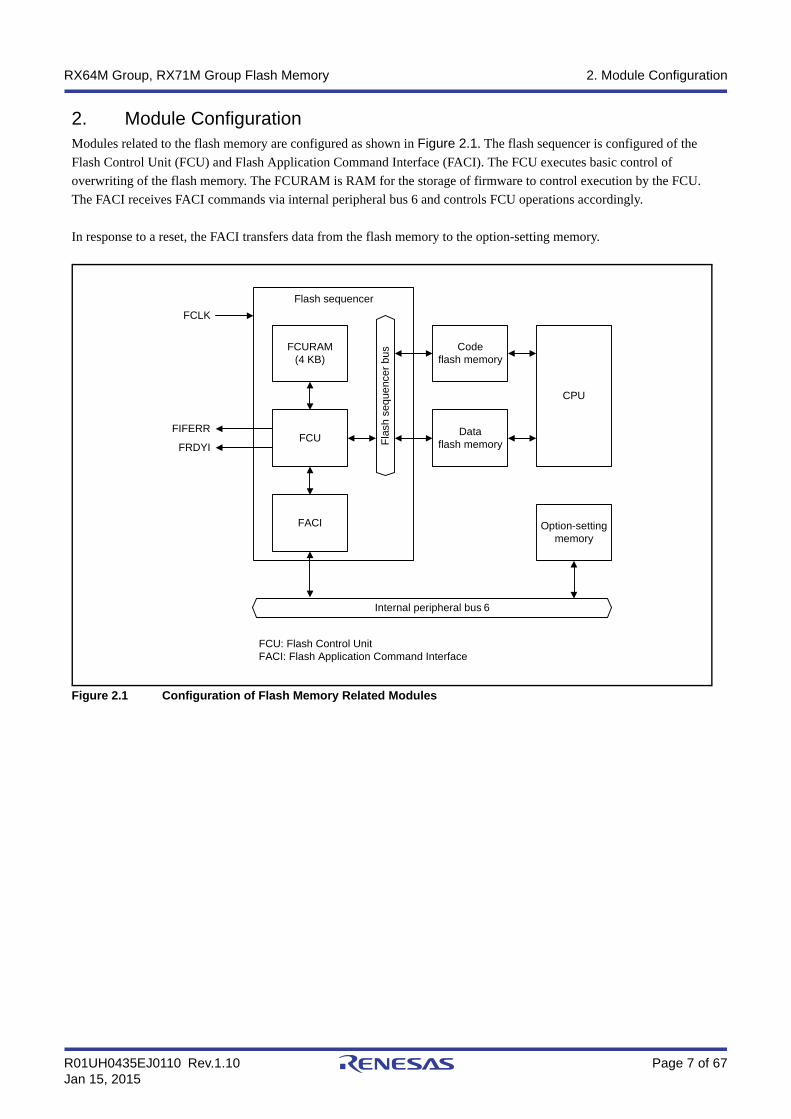
RX64M Group, RX71M Group Flash Memory 2. Module Configuration
2. Module ConfigurationModules related to the flash memory are configured as shown in Figure 2.1. The flash sequencer is configured of the Flash Control Unit (FCU) and Flash Application Command Interface (FACI). The FCU executes basic control of overwriting of the flash memory. The FCURAM is RAM for the storage of firmware to control execution by the FCU. The FACI receives FACI commands via internal peripheral bus 6 and controls FCU operations accordingly.
In response to a reset, the FACI transfers data from the flash memory to the option-setting memory.
Figure 2.1 Configuration of Flash Memory Related Modules
Flash sequencer
Option-setting memory
FACI
FCU
FCURAM(4 KB)
CPU
Dataflash memory
Codeflash memory
Internal peripheral bus 6
FCU: Flash Control UnitFACI: Flash Application Command Interface
FCLK
FIFERR
FRDYI Fla
sh s
eque
nce
r bu
s
R01UH0435EJ0110 Rev.1.10 Page 8 of 67Jan 15, 2015
RX64M Group, RX71M Group Flash Memory 3. Address Space
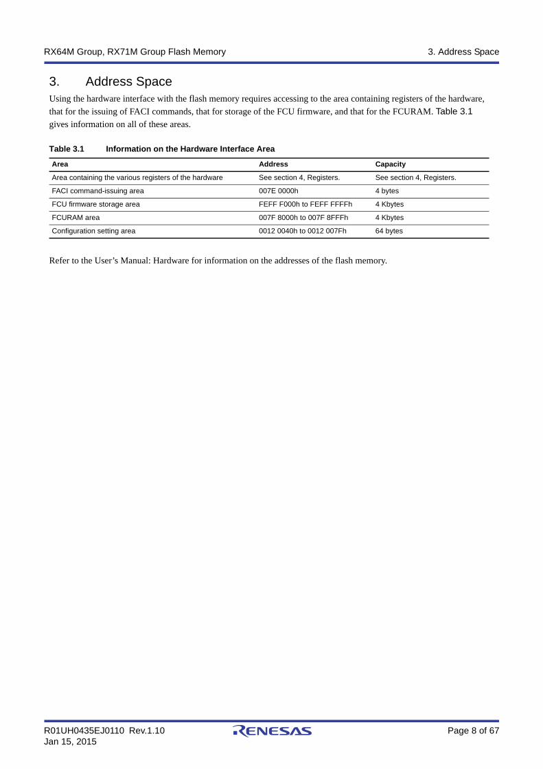
3. Address SpaceUsing the hardware interface with the flash memory requires accessing to the area containing registers of the hardware, that for the issuing of FACI commands, that for storage of the FCU firmware, and that for the FCURAM. Table 3.1 gives information on all of these areas.
Refer to the User’s Manual: Hardware for information on the addresses of the flash memory.
Table 3.1 Information on the Hardware Interface Area
Area Address Capacity
Area containing the various registers of the hardware See section 4, Registers. See section 4, Registers.
FACI command-issuing area 007E 0000h 4 bytes
FCU firmware storage area FEFF F000h to FEFF FFFFh 4 Kbytes
FCURAM area 007F 8000h to 007F 8FFFh 4 Kbytes
Configuration setting area 0012 0040h to 0012 007Fh 64 bytes
R01UH0435EJ0110 Rev.1.10 Page 9 of 67Jan 15, 2015
RX64M Group, RX71M Group Flash Memory 4. Registers
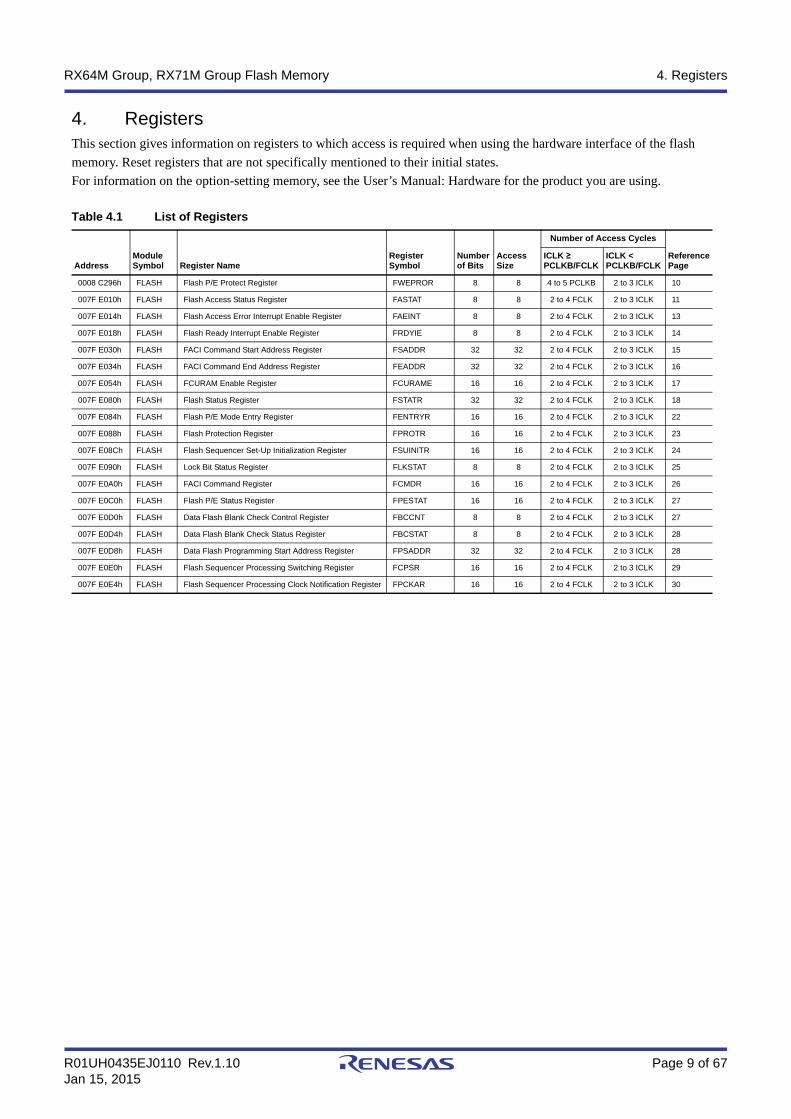
4. RegistersThis section gives information on registers to which access is required when using the hardware interface of the flash memory. Reset registers that are not specifically mentioned to their initial states.For information on the option-setting memory, see the User’s Manual: Hardware for the product you are using.
Table 4.1 List of Registers
AddressModule Symbol Register Name
Register Symbol
Number of Bits
Access Size
Number of Access Cycles
Reference Page
ICLK ≥ PCLKB/FCLK
ICLK < PCLKB/FCLK
0008 C296h FLASH Flash P/E Protect Register FWEPROR 8 8 4 to 5 PCLKB 2 to 3 ICLK 10
007F E010h FLASH Flash Access Status Register FASTAT 8 8 2 to 4 FCLK 2 to 3 ICLK 11
007F E014h FLASH Flash Access Error Interrupt Enable Register FAEINT 8 8 2 to 4 FCLK 2 to 3 ICLK 13
007F E018h FLASH Flash Ready Interrupt Enable Register FRDYIE 8 8 2 to 4 FCLK 2 to 3 ICLK 14
007F E030h FLASH FACI Command Start Address Register FSADDR 32 32 2 to 4 FCLK 2 to 3 ICLK 15
007F E034h FLASH FACI Command End Address Register FEADDR 32 32 2 to 4 FCLK 2 to 3 ICLK 16
007F E054h FLASH FCURAM Enable Register FCURAME 16 16 2 to 4 FCLK 2 to 3 ICLK 17
007F E080h FLASH Flash Status Register FSTATR 32 32 2 to 4 FCLK 2 to 3 ICLK 18
007F E084h FLASH Flash P/E Mode Entry Register FENTRYR 16 16 2 to 4 FCLK 2 to 3 ICLK 22
007F E088h FLASH Flash Protection Register FPROTR 16 16 2 to 4 FCLK 2 to 3 ICLK 23
007F E08Ch FLASH Flash Sequencer Set-Up Initialization Register FSUINITR 16 16 2 to 4 FCLK 2 to 3 ICLK 24
007F E090h FLASH Lock Bit Status Register FLKSTAT 8 8 2 to 4 FCLK 2 to 3 ICLK 25
007F E0A0h FLASH FACI Command Register FCMDR 16 16 2 to 4 FCLK 2 to 3 ICLK 26
007F E0C0h FLASH Flash P/E Status Register FPESTAT 16 16 2 to 4 FCLK 2 to 3 ICLK 27
007F E0D0h FLASH Data Flash Blank Check Control Register FBCCNT 8 8 2 to 4 FCLK 2 to 3 ICLK 27
007F E0D4h FLASH Data Flash Blank Check Status Register FBCSTAT 8 8 2 to 4 FCLK 2 to 3 ICLK 28
007F E0D8h FLASH Data Flash Programming Start Address Register FPSADDR 32 32 2 to 4 FCLK 2 to 3 ICLK 28
007F E0E0h FLASH Flash Sequencer Processing Switching Register FCPSR 16 16 2 to 4 FCLK 2 to 3 ICLK 29
007F E0E4h FLASH Flash Sequencer Processing Clock Notification Register FPCKAR 16 16 2 to 4 FCLK 2 to 3 ICLK 30
R01UH0435EJ0110 Rev.1.10 Page 10 of 67Jan 15, 2015
RX64M Group, RX71M Group Flash Memory 4. Registers
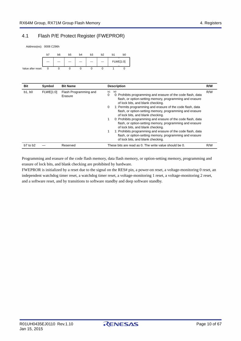
4.1 Flash P/E Protect Register (FWEPROR)
Programming and erasure of the code flash memory, data flash memory, or option-setting memory, programming and erasure of lock bits, and blank checking are prohibited by hardware.FWEPROR is initialized by a reset due to the signal on the RES# pin, a power-on reset, a voltage-monitoring 0 reset, an independent watchdog timer reset, a watchdog timer reset, a voltage-monitoring 1 reset, a voltage-monitoring 2 reset, and a software reset, and by transitions to software standby and deep software standby.
Address(es): 0008 C296h
b7 b6 b5 b4 b3 b2 b1 b0
— — — — — — FLWE[1:0]
Value after reset: 0 0 0 0 0 0 1 0
Bit Symbol Bit Name Description R/W
b1, b0 FLWE[1:0] Flash Programming and Erasure
b1 b00 0: Prohibits programming and erasure of the code flash, data
flash, or option-setting memory, programming and erasure of lock bits, and blank checking.
0 1: Permits programming and erasure of the code flash, data flash, or option-setting memory, programming and erasure of lock bits, and blank checking.
1 0: Prohibits programming and erasure of the code flash, data flash, or option-setting memory, programming and erasure of lock bits, and blank checking.
1 1: Prohibits programming and erasure of the code flash, data flash, or option-setting memory, programming and erasure of lock bits, and blank checking.
R/W
b7 to b2 — Reserved These bits are read as 0. The write value should be 0. R/W
R01UH0435EJ0110 Rev.1.10 Page 11 of 67Jan 15, 2015
RX64M Group, RX71M Group Flash Memory 4. Registers
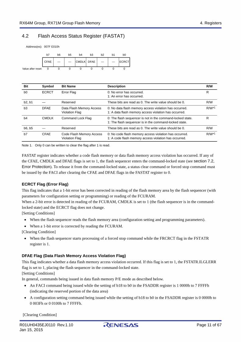
4.2 Flash Access Status Register (FASTAT)
Note 1. Only 0 can be written to clear the flag after 1 is read.
FASTAT register indicates whether a code flash memory or data flash memory access violation has occurred. If any of the CFAE, CMDLK and DFAE flags is set to 1, the flash sequencer enters the command-locked state (see section 7.2,
Error Protection). To release it from the command-locked state, a status clear command or forced stop command must be issued by the FACI after clearing the CFAE and DFAE flags in the FASTAT register to 0.
ECRCT Flag (Error Flag)
This flag indicates that a 1-bit error has been corrected in reading of the flash memory area by the flash sequencer (with parameters for configuration setting or programming) or reading of the FCURAM.When a 2-bit error is detected in reading of the FCURAM, CMDLK is set to 1 (the flash sequencer is in the command-locked state) and the ECRCT flag does not change.[Setting Conditions] When the flash sequencer reads the flash memory area (configuration setting and programming parameters). When a 1-bit error is corrected by reading the FCURAM.
[Clearing Condition] When the flash sequencer starts processing of a forced stop command while the FRCRCT flag in the FSTATR
register is 1.
DFAE Flag (Data Flash Memory Access Violation Flag)
This flag indicates whether a data flash memory access violation occurred. If this flag is set to 1, the FSTATR.ILGLERR flag is set to 1, placing the flash sequencer in the command-locked state.[Setting Conditions]In general, commands being issued in data flash memory P/E mode as described below. An FACI command being issued while the setting of b18 to b0 in the FSADDR register is 1 0000h to 7 FFFFh
(indicating the reserved portion of the data area) A configuration setting command being issued while the setting of b18 to b0 in the FSADDR register is 0 0000h to
0 003Fh or 0 0100h to 7 FFFFh.
[Clearing Condition]
Address(es): 007F E010h
b7 b6 b5 b4 b3 b2 b1 b0
CFAE — — CMDLK DFAE — — ECRCT
Value after reset: 0 0 0 0 0 0 0 0
Bit Symbol Bit Name Description R/W
b0 ECRCT Error Flag 0: No error has occurred.1: An error has occurred.
R
b2, b1 — Reserved These bits are read as 0. The write value should be 0. R/W
b3 DFAE Data Flash Memory Access Violation Flag
0: No data flash memory access violation has occurred.1: A data flash memory access violation has occurred.
R/W*1
b4 CMDLK Command Lock Flag 0: The flash sequencer is not in the command-locked state.1: The flash sequencer is in the command-locked state.
R
b6, b5 — Reserved These bits are read as 0. The write value should be 0. R/W
b7 CFAE Code Flash Memory Access Violation Flag
0: No code flash memory access violation has occurred.1: A code flash memory access violation has occurred.
R/W*1
R01UH0435EJ0110 Rev.1.10 Page 12 of 67Jan 15, 2015
RX64M Group, RX71M Group Flash Memory 4. Registers
0 being written after reading of 1.
CMDLK Flag (Command Lock Flag)
This flag indicates that the flash sequencer is in the command-locked state.[Setting Condition] The flash sequencer detects an error and enters the command-locked state.
[Clearing Condition] The flash sequencer starting to process a status clear or forced stop command while the CFAE or DFAE flag in the
FASTAT register is 0.
CFAE Flag (Code Flash Memory Access Violation Flag)
This flag indicates whether a code flash memory access violation has occurred. If this flag is set to 1, the FSTATR.ILGLERR flag is set to 1, placing the flash sequencer in the command-locked state.[Setting Conditions]An FACI command being issued in code flash memory P/E mode while settings are as follows: The setting of b23 to b0 in the FSADDR register is 00 0000h to BF FFFFh (reserved portion of the user area).
[Clearing Condition] 0 being written after reading of 1.
R01UH0435EJ0110 Rev.1.10 Page 13 of 67Jan 15, 2015
RX64M Group, RX71M Group Flash Memory 4. Registers
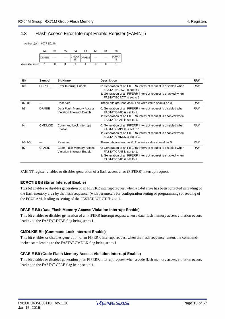
4.3 Flash Access Error Interrupt Enable Register (FAEINT)
FAEINT register enables or disables generation of a flash access error (FIFERR) interrupt request.
ECRCTIE Bit (Error Interrupt Enable)
This bit enables or disables generation of an FIFERR interrupt request when a 1-bit error has been corrected in reading of the flash memory area by the flash sequencer (with parameters for configuration setting or programming) or reading of the FCURAM, leading to setting of the FASTAT.ECRCT flag to 1.
DFAEIE Bit (Data Flash Memory Access Violation Interrupt Enable)
This bit enables or disables generation of an FIFERR interrupt request when a data flash memory access violation occurs leading to the FASTAT.DFAE flag being set to 1.
CMDLKIE Bit (Command Lock Interrupt Enable)
This bit enables or disables generation of an FIFERR interrupt request when the flash sequencer enters the command-locked state leading to the FASTAT.CMDLK flag being set to 1.
CFAEIE Bit (Code Flash Memory Access Violation Interrupt Enable)
This bit enables or disables generation of an FIFERR interrupt request when a code flash memory access violation occurs leading to the FASTAT.CFAE flag being set to 1.
Address(es): 007F E014h
b7 b6 b5 b4 b3 b2 b1 b0
CFAEIE — — CMDLKIE
DFAEIE — — ECRCTIE
Value after reset: 1 0 0 1 1 0 0 1
Bit Symbol Bit Name Description R/W
b0 ECRCTIE Error Interrupt Enable 0: Generation of an FIFERR interrupt request is disabled when FASTAT.ECRCT is set to 1.
1: Generation of an FIFERR interrupt request is enabled when FASTAT.ECRCT is set to 1.
R/W
b2, b1 — Reserved These bits are read as 0. The write value should be 0. R/W
b3 DFAEIE Data Flash Memory Access Violation Interrupt Enable
0: Generation of an FIFERR interrupt request is disabled when FASTAT.DFAE is set to 1.
1: Generation of an FIFERR interrupt request is enabled when FASTAT.DFAE is set to 1.
R/W
b4 CMDLKIE Command Lock Interrupt Enable
0: Generation of an FIFERR interrupt request is disabled when FASTAT.CMDLK is set to 1.
1: Generation of an FIFERR interrupt request is enabled when FASTAT.CMDLK is set to 1.
R/W
b6, b5 — Reserved These bits are read as 0. The write value should be 0. R/W
b7 CFAEIE Code Flash Memory Access Violation Interrupt Enable
0: Generation of an FIFERR interrupt request is disabled when FASTAT.CFAE is set to 1.
1: Generation of an FIFERR interrupt request is enabled when FASTAT.CFAE is set to 1.
R/W
R01UH0435EJ0110 Rev.1.10 Page 14 of 67Jan 15, 2015
RX64M Group, RX71M Group Flash Memory 4. Registers
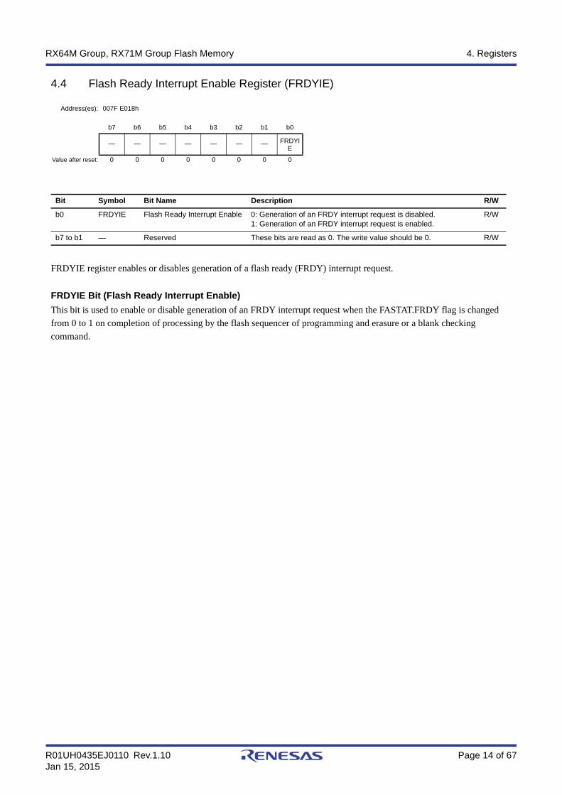
4.4 Flash Ready Interrupt Enable Register (FRDYIE)
FRDYIE register enables or disables generation of a flash ready (FRDY) interrupt request.
FRDYIE Bit (Flash Ready Interrupt Enable)
This bit is used to enable or disable generation of an FRDY interrupt request when the FASTAT.FRDY flag is changed from 0 to 1 on completion of processing by the flash sequencer of programming and erasure or a blank checking command.
Address(es): 007F E018h
b7 b6 b5 b4 b3 b2 b1 b0
— — — — — — — FRDYIE
Value after reset: 0 0 0 0 0 0 0 0
Bit Symbol Bit Name Description R/W
b0 FRDYIE Flash Ready Interrupt Enable 0: Generation of an FRDY interrupt request is disabled.1: Generation of an FRDY interrupt request is enabled.
R/W
b7 to b1 — Reserved These bits are read as 0. The write value should be 0. R/W
R01UH0435EJ0110 Rev.1.10 Page 15 of 67Jan 15, 2015
RX64M Group, RX71M Group Flash Memory 4. Registers
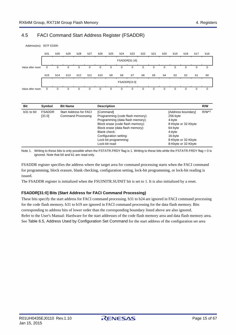
4.5 FACI Command Start Address Register (FSADDR)
Note 1. Writing to these bits is only possible when the FSTATR.FRDY flag is 1. Writing to these bits while the FSTATR.FRDY flag = 0 is ignored. Note that b0 and b1 are read-only.
FSADDR register specifies the address where the target area for command processing starts when the FACI command for programming, block erasure, blank checking, configuration setting, lock-bit programming, or lock-bit reading is issued. The FSADDR register is initialized when the FSUINITR.SUINIT bit is set to 1. It is also initialized by a reset.
FSADDR[31:0] Bits (Start Address for FACI Command Processing)
These bits specify the start address for FACI command processing. b31 to b24 are ignored in FACI command processing for the code flash memory. b31 to b19 are ignored in FACI command processing for the data flash memory. Bits corresponding to address bits of lower order than the corresponding boundary listed above are also ignored.Refer to the User's Manual: Hardware for the start addresses of the code flash memory area and data flash memory area. See Table 6.5, Address Used by Configuration Set Command for the start address of the configuration set area
Address(es): 007F E030h
b31 b30 b29 b28 b27 b26 b25 b24 b23 b22 b21 b20 b19 b18 b17 b16
FSADDR[31:16]
Value after reset: 0 0 0 0 0 0 0 0 0 0 0 0 0 0 0 0
b15 b14 b13 b12 b11 b10 b9 b8 b7 b6 b5 b4 b3 b2 b1 b0
FSADDR[15:0]
Value after reset: 0 0 0 0 0 0 0 0 0 0 0 0 0 0 0 0
Bit Symbol Bit Name Description R/W
b31 to b0 FSADDR[31:0]
Start Address for FACI Command Processing
[Command]Programming (code flash memory):Programming (data flash memory):Block erase (code flash memory):Block erase (data flash memory):Blank check:Configuration setting:Lock-bit programming:Lock-bit read:
[Address boundary]256-byte4-byte8-Kbyte or 32-Kbyte64-byte4-byte16-byte8-Kbyte or 32-Kbyte8-Kbyte or 32-Kbyte
R/W*1
R01UH0435EJ0110 Rev.1.10 Page 16 of 67Jan 15, 2015
RX64M Group, RX71M Group Flash Memory 4. Registers
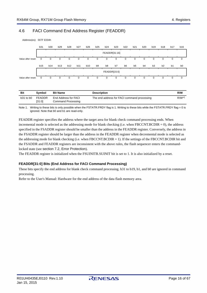
4.6 FACI Command End Address Register (FEADDR)
Note 1. Writing to these bits is only possible when the FSTATR.FRDY flag is 1. Writing to these bits while the FSTATR.FRDY flag = 0 is ignored. Note that b0 and b1 are read-only.
FEADDR register specifies the address where the target area for blank check command processing ends. When incremental mode is selected as the addressing mode for blank checking (i.e. when FBCCNT.BCDIR = 0), the address specified in the FSADDR register should be smaller than the address in the FEADDR register. Conversely, the address in the FSADDR register should be larger than the address in the FEADDR register when decremental mode is selected as the addressing mode for blank checking (i.e. when FBCCNT.BCDIR = 1). If the settings of the FBCCNT.BCDIR bit and the FSADDR and FEADDR registers are inconsistent with the above rules, the flash sequencer enters the command-locked state (see section 7.2, Error Protection).The FEADDR register is initialized when the FSUINITR.SUINIT bit is set to 1. It is also initialized by a reset.
FEADDR[31:0] Bits (End Address for FACI Command Processing)
These bits specify the end address for blank check command processing. b31 to b19, b1, and b0 are ignored in command processing.Refer to the User's Manual: Hardware for the end address of the data flash memory area.
Address(es): 007F E034h
b31 b30 b29 b28 b27 b26 b25 b24 b23 b22 b21 b20 b19 b18 b17 b16
FEADDR[31:16]
Value after reset: 0 0 0 0 0 0 0 0 0 0 0 0 0 0 0 0
b15 b14 b13 b12 b11 b10 b9 b8 b7 b6 b5 b4 b3 b2 b1 b0
FEADDR[15:0]
Value after reset: 0 0 0 0 0 0 0 0 0 0 0 0 0 0 0 0
Bit Symbol Bit Name Description R/W
b31 to b0 FEADDR[31:0]
End Address for FACI Command Processing
The end address for FACI command processing R/W*1
R01UH0435EJ0110 Rev.1.10 Page 17 of 67Jan 15, 2015
RX64M Group, RX71M Group Flash Memory 4. Registers
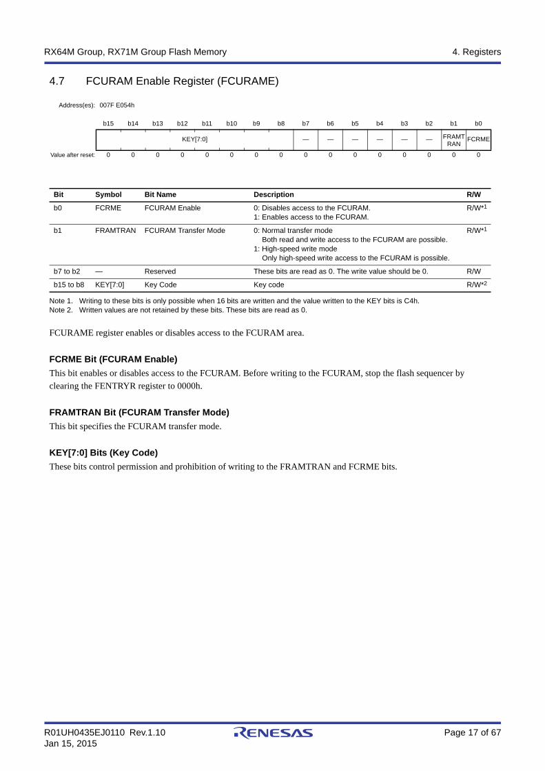
4.7 FCURAM Enable Register (FCURAME)
Note 1. Writing to these bits is only possible when 16 bits are written and the value written to the KEY bits is C4h.Note 2. Written values are not retained by these bits. These bits are read as 0.
FCURAME register enables or disables access to the FCURAM area.
FCRME Bit (FCURAM Enable)
This bit enables or disables access to the FCURAM. Before writing to the FCURAM, stop the flash sequencer by clearing the FENTRYR register to 0000h.
FRAMTRAN Bit (FCURAM Transfer Mode)
This bit specifies the FCURAM transfer mode.
KEY[7:0] Bits (Key Code)
These bits control permission and prohibition of writing to the FRAMTRAN and FCRME bits.
Address(es): 007F E054h
b15 b14 b13 b12 b11 b10 b9 b8 b7 b6 b5 b4 b3 b2 b1 b0
KEY[7:0] — — — — — — FRAMTRAN
FCRME
Value after reset: 0 0 0 0 0 0 0 0 0 0 0 0 0 0 0 0
Bit Symbol Bit Name Description R/W
b0 FCRME FCURAM Enable 0: Disables access to the FCURAM.1: Enables access to the FCURAM.
R/W*1
b1 FRAMTRAN FCURAM Transfer Mode 0: Normal transfer modeBoth read and write access to the FCURAM are possible.
1: High-speed write modeOnly high-speed write access to the FCURAM is possible.
R/W*1
b7 to b2 — Reserved These bits are read as 0. The write value should be 0. R/W
b15 to b8 KEY[7:0] Key Code Key code R/W*2
R01UH0435EJ0110 Rev.1.10 Page 18 of 67Jan 15, 2015
RX64M Group, RX71M Group Flash Memory 4. Registers
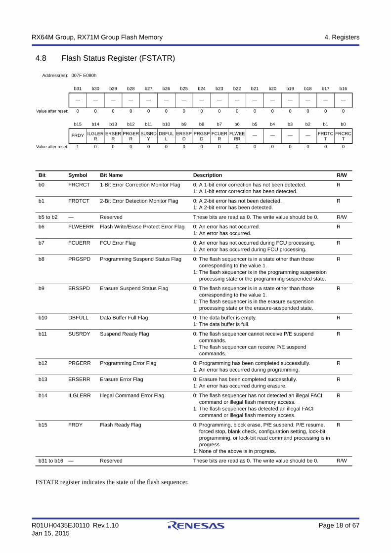
4.8 Flash Status Register (FSTATR)
FSTATR register indicates the state of the flash sequencer.
Address(es): 007F E080h
b31 b30 b29 b28 b27 b26 b25 b24 b23 b22 b21 b20 b19 b18 b17 b16
— — — — — — — — — — — — — — — —
Value after reset: 0 0 0 0 0 0 0 0 0 0 0 0 0 0 0 0
b15 b14 b13 b12 b11 b10 b9 b8 b7 b6 b5 b4 b3 b2 b1 b0
FRDY ILGLERR
ERSERR
PRGERR
SUSRDY
DBFULL
ERSSPD
PRGSPD
FCUERR
FLWEERR
— — — — FRDTCT
FRCRCT
Value after reset: 1 0 0 0 0 0 0 0 0 0 0 0 0 0 0 0
Bit Symbol Bit Name Description R/W
b0 FRCRCT 1-Bit Error Correction Monitor Flag 0: A 1-bit error correction has not been detected.1: A 1-bit error correction has been detected.
R
b1 FRDTCT 2-Bit Error Detection Monitor Flag 0: A 2-bit error has not been detected.1: A 2-bit error has been detected.
R
b5 to b2 — Reserved These bits are read as 0. The write value should be 0. R/W
b6 FLWEERR Flash Write/Erase Protect Error Flag 0: An error has not occurred.1: An error has occurred.
R
b7 FCUERR FCU Error Flag 0: An error has not occurred during FCU processing.1: An error has occurred during FCU processing.
R
b8 PRGSPD Programming Suspend Status Flag 0: The flash sequencer is in a state other than those corresponding to the value 1.
1: The flash sequencer is in the programming suspension processing state or the programming suspended state.
R
b9 ERSSPD Erasure Suspend Status Flag 0: The flash sequencer is in a state other than those corresponding to the value 1.
1: The flash sequencer is in the erasure suspension processing state or the erasure-suspended state.
R
b10 DBFULL Data Buffer Full Flag 0: The data buffer is empty.1: The data buffer is full.
R
b11 SUSRDY Suspend Ready Flag 0: The flash sequencer cannot receive P/E suspend commands.
1: The flash sequencer can receive P/E suspend commands.
R
b12 PRGERR Programming Error Flag 0: Programming has been completed successfully.1: An error has occurred during programming.
R
b13 ERSERR Erasure Error Flag 0: Erasure has been completed successfully.1: An error has occurred during erasure.
R
b14 ILGLERR Illegal Command Error Flag 0: The flash sequencer has not detected an illegal FACI command or illegal flash memory access.
1: The flash sequencer has detected an illegal FACI command or illegal flash memory access.
R
b15 FRDY Flash Ready Flag 0: Programming, block erase, P/E suspend, P/E resume, forced stop, blank check, configuration setting, lock-bit programming, or lock-bit read command processing is in progress.
1: None of the above is in progress.
R
b31 to b16 — Reserved These bits are read as 0. The write value should be 0. R/W
R01UH0435EJ0110 Rev.1.10 Page 19 of 67Jan 15, 2015
RX64M Group, RX71M Group Flash Memory 4. Registers
FRCRCT Flag (1-Bit Error Correction Monitor Flag)
This flag indicates that a 1-bit error has been corrected by reading FCURAM by the FCU. When the FRCRCT flag is 1, the flash sequencer is not in the command locked state.[Clearing Condition] When the flash sequencer starts processing of a forced stop command.
After the FCU is initialized by issuing a forced stop command, reload the FCU firmware into the FCURAM.
FRDTCT Flag (2-Bit Error Detection Monitor Flag)
This flag indicates that a 2-bit error has been detected by reading FCURAM by the FCU. When the FRDTCT flag is 1, the flash sequencer is in the command locked state.[Clearing Condition] When the flash sequencer starts processing of a forced stop command.
After the FCU is initialized by issuing a forced stop command, reload the FCU firmware into the FCURAM.
FLWEERR Flag (Flash Write/Erase Protect Error Flag)
This flag indicates a violation of the flash memory overwrite protection setting in the FWEPROR register. If this flag is 1, the flash sequencer is in the command-locked state.[Clearing Condition] The flash sequencer starts processing of a forced stop command.
FCUERR Flag (FCU Error Flag)
This flag indicates that an error has occurred during FCU processing. If this flag is 1, the flash sequencer is in the command-locked state.[Clearing Condition] The flash sequencer starts processing of a forced stop command.
When this flag is 1, issue a forced stop command and initialize the FCU, and then reload the FCU firmware into the FCURAM.
PRGSPD Flag (Programming Suspend Status Flag)
This flag indicates that the flash sequencer is in the programming suspension processing state or programming suspended state.[Setting Condition] The flash sequencer starts processing in response to a programming suspend command.
[Clearing Conditions] Reception of the P/E resume command by the flash sequencer
(after write access to the FACI command-issuing area is completed). The flash sequencer starts processing of a forced stop command.
ERSSPD Flag (Erasure Suspend Status Flag)
This flag indicates that the flash sequencer is in the erasure suspension processing state or erasure suspended state.[Setting Condition] The flash sequencer starts processing in response to an erasure suspend command.
[Clearing Conditions] Reception of the P/E resume command by the flash sequencer
(after write access to the FACI command-issuing area is completed). The flash sequencer starts processing of a forced stop command.
R01UH0435EJ0110 Rev.1.10 Page 20 of 67Jan 15, 2015
RX64M Group, RX71M Group Flash Memory 4. Registers
DBFULL Flag (Data Buffer Full Flag)
This flag indicates the state of the data buffer when a programming command is issued. The FACI incorporates a buffer for write data (data buffer). When data for writing to the flash memory are issued to the FACI command-issuing area while the data buffer is full, the FACI inserts a wait cycle in the peripheral bus 6.[Setting Condition] The data buffer becomes full while programming commands are being issued.
[Clearing Condition] The data buffer becomes empty.
SUSRDY Flag (Suspend Ready Flag)
This flag indicates whether the flash sequencer can receive a P/E suspend command.[Setting Condition] After starting programming/erasure processing, the flash sequencer enters a state in which P/E suspend commands
can be received.[Clearing Conditions] Reception of the P/E suspend command or forced stop command by the flash sequencer (after write access to the
FACI command-issuing area is completed). During programming or erasure, the flash sequencer enters the command-locked state. Programming or erasure has been completed.
PRGERR Flag (Programming Error Flag)
This flag indicates the result of programming of the flash memory. If this flag is 1, the flash sequencer is in the command-locked state.[Setting Conditions] An error occurs during programming. A programming or lock-bit programming command is issued for an area where the lock bit setting is for protection.
[Clearing Condition] The flash sequencer starts processing of a status clear or forced stop command.
ERSERR Flag (Erasure Error Flag)
This flag indicates the result of erasure of the flash memory. If this flag is 1, the flash sequencer is in the command-locked state.[Setting Conditions] An error has occurred during erasure. A block erase command is issued for an area where the lock bit setting is for protection.
[Clearing Condition] The flash sequencer starts processing of a status clear or forced stop command.
ILGLERR Flag (Illegal Command Error Flag)
This flag indicates that the flash sequencer has detected an illegal FACI command or flash memory access. If this flag is 1, the flash sequencer is in the command-locked state.[Setting Conditions] (See section 7.2, Error Protection) The flash sequencer has detected an illegal command. The flash sequencer has detected illegal flash memory access. The setting of the FENTRYR register is invalid.
R01UH0435EJ0110 Rev.1.10 Page 21 of 67Jan 15, 2015
RX64M Group, RX71M Group Flash Memory 4. Registers
[Clearing Condition] The flash sequencer starts processing of a status clear or forced stop command while the DFAE and CFAE flag in
the FASTAT register is 0.If the flash sequencer completes processing of a status clear or forced stop command while the CFAE or DFAE flag in the FASTAT register is 1, this flag is set to 1. This flag is temporarily set to 0 during processing of a forced stop command, and is re-set to 1 when the CFAE or DFAE flag is detected as 1 on completion of command processing.
FRDY Flag (Flash Ready Flag)
This flag indicates the command processing state of the flash sequencer.[Setting Conditions] The flash sequencer completes command processing. The flash sequencer receives a P/E suspend command and suspends programming of the flash memory. The flash sequencer has received a forced stop command and ended command processing.
[Clearing Conditions] The flash sequencer has received an FACI command. For programming and configuration setting, the first write access to the FACI command-issuing area. For other commands, the last write access to the FACI command-issuing area.
R01UH0435EJ0110 Rev.1.10 Page 22 of 67Jan 15, 2015
RX64M Group, RX71M Group Flash Memory 4. Registers
4.9 Flash P/E Mode Entry Register (FENTRYR)
Note 1. Writing to these bits is only possible when the FSTATR.FRDY flag is 1. Writing to these bits while the FSTATR.FRDY flag = 0 is ignored.
Note 2. Writing to these bits is only possible when 16 bits are written and the value written to the KEY bits is AAh.Note 3. Written values are not retained by these bits. These bits are read as 0.
FENTRYR is used to specify code flash memory P/E mode and data flash memory P/E mode. To specify code flash memory P/E mode or data flash memory P/E mode so that the flash sequencer can receive FACI commands, set either the FENTRYD or FENTRYC bit to 1 to place the flash sequencer in P/E mode.Note that setting this register to a value other than 0001h and 0080h, the FSTATR.ILGLERR flag will be set to 1, leading to the flash sequencer being placed in the command-locked state.The FENTRYR register is initialized when the FSUINITR.SUINIT bit is set to 1. It is also initialized by a reset.
FENTRYC Bit (Code Flash Memory P/E Mode Entry)
This bit specifies the P/E mode for code flash memory.[Setting Condition] 1 being written to the FENTRYC bit while writing to FENTRYR is enabled and FENTRYR is 0000h.
[Clearing Conditions] 8 bits being written to FENTRYR while the FSTATR.FRDY flag is 1. A value other than AAh is specified in the KEY bits and 16 bits are written to FENTRYR while the
FSTATR.FRDY flag is 1. 0 being written to the FENTRYC bit while writing to FENTRYR is enabled. FENTRYR being written to while writing to FENTRYR is enabled and the value of FENTRYR is other than 0000h.
FENTRYD Bit (Data Flash Memory P/E Mode Entry)
This bit specifies the P/E mode for data flash memory.[Setting Condition] 1 being written to the FENTRYR.FENTRYD bit while writing to FENTRYR is enabled and FENTRYR is 0000h.
[Clearing Conditions] 8 bits being written to FENTRYR while the FSTATR.FRDY flag is 1. Writing of 16 bits to FENTRYR with a value other than AAh specified for the KEY bits while the FSTATR.FRDY
flag is 1. 0 being written to the FENTRYD bit while writing to FENTRYR is enabled. FENTRYR being written to while writing to FENTRYR is enabled and the value of FENTRYR is other than 0000h.
Address(es): 007F E084h
b15 b14 b13 b12 b11 b10 b9 b8 b7 b6 b5 b4 b3 b2 b1 b0
KEY[7:0] FENTRYD
— — — — — — FENTRYC
Value after reset: 0 0 0 0 0 0 0 0 0 0 0 0 0 0 0 0
Bit Symbol Bit Name Description R/W
b0 FENTRYC Code Flash Memory P/E Mode Entry
0: Code flash memory is in read mode.1: Code flash memory is in P/E mode.
R/W*1, *2
b6 to b1 — Reserved These bits are read as 0. The write value should be 0. R/W
b7 FENTRYD Data Flash Memory P/E Mode Entry
0: Data flash memory is in read mode.1: Data flash memory is in P/E mode.
R/W*1, *2
b15 to b8 KEY[7:0] Key Code Key code R/W*3
R01UH0435EJ0110 Rev.1.10 Page 23 of 67Jan 15, 2015
RX64M Group, RX71M Group Flash Memory 4. Registers
KEY[7:0] Bits (Key Code)
These bits control permission and prohibition of writing to the FENTRYD and FENTRYC bits.
4.10 Flash Protection Register (FPROTR)
Note 1. Writing to these bits is only possible when 16 bits are written and the value written to the KEY bits is 55h.Note 2. Written values are not retained by these bits. These bits are read as 0.
FPROTR enables or disables protection by the lock bits of the code flash memory against programming and erasure. The FPROTR register is initialized when the FSUINITR.SUINIT bit is set to 1. It is also initialized by a reset.
FPROTCN Bit (Lock Bit Protection Cancel)
This bit enables or disables protection by the lock bits of the code flash memory against programming and erasure.[Setting Condition] 1 being written to the FPROTCN bit while writing to FPROTR is enabled and the value of FENTRYR is other than
0000h.[Clearing Conditions] 8 bits being written to FPROTR Writing of 16 bits to FPROTR with a value other than 55h specified for the KEY bits 0 being written to the FPROTRCN bit while writing to FPROTR is enabled The value of FENTRYR being 0000h
KEY[7:0] Bits (Key Code)
These bits control permission and prohibition of writing to the FPROTCN bit.
Address(es): 007F E088h
b15 b14 b13 b12 b11 b10 b9 b8 b7 b6 b5 b4 b3 b2 b1 b0
KEY[7:0] — — — — — — — FPROTCN
Value after reset: 0 0 0 0 0 0 0 0 0 0 0 0 0 0 0 0
Bit Symbol Bit Name Description R/W
b0 FPROTCN Lock Bit Protection Cancel 0: Enables protection by the lock bits.1: Disables protection by the lock bits.
R/W*1
b7 to b1 — Reserved These bits are read as 0. The write value should be 0. R/W
b15 to b8 KEY[7:0] Key Code Key code R/W*2
R01UH0435EJ0110 Rev.1.10 Page 24 of 67Jan 15, 2015
RX64M Group, RX71M Group Flash Memory 4. Registers
4.11 Flash Sequencer Set-Up Initialization Register (FSUINITR)
Note 1. Writing to these bits is only possible when the FSTATR.FRDY flag is 1. Writing to these bits while the FSTATR.FRDY flag = 0 is ignored.
Note 2. Writing to these bits is only possible when 16 bits are written and the value written to the KEY bits is 2Dh.Note 3. Written values are not retained by these bits. This bit is read as 0.
FSUINITR is used for initialization of the flash sequencer set-up.
SUINIT Bit (Set-Up Initialization)
This bit initializes the following flash sequencer set-up registers. FEADDR FPROTR FCPSR FSADDR FENTRYR FBCCNT
KEY[7:0] Bits (Key Code)
These bits control permission and prohibition of writing to the SUINIT bit.
Address(es): 007F E08Ch
b15 b14 b13 b12 b11 b10 b9 b8 b7 b6 b5 b4 b3 b2 b1 b0
KEY[7:0] — — — — — — — SUINIT
Value after reset: 0 0 0 0 0 0 0 0 0 0 0 0 0 0 0 0
Bit Symbol Bit Name Description R/W
b0 SUINIT Set-Up Initialization 0: The FEADDR, FPROTR, FCPSR, FSADDR, FENTRYR, and FBCCNT flash sequencer set-up registers keep their current values.
1: The FEADDR, FPROTR, FCPSR, FSADDR, FENTRYR, and FBCCNT flash sequencer set-up registers are initialized.
R/W*1, *2
b7 to b1 — Reserved These bits are read as 0. The write value should be 0. R/W
b15 to b8 KEY[7:0] Key Code Key code R/W*3
R01UH0435EJ0110 Rev.1.10 Page 25 of 67Jan 15, 2015
RX64M Group, RX71M Group Flash Memory 4. Registers
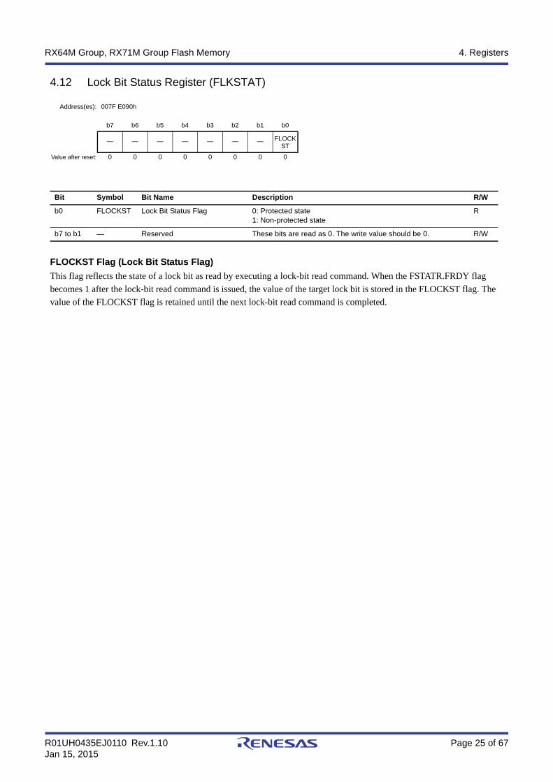
4.12 Lock Bit Status Register (FLKSTAT)
FLOCKST Flag (Lock Bit Status Flag)
This flag reflects the state of a lock bit as read by executing a lock-bit read command. When the FSTATR.FRDY flag becomes 1 after the lock-bit read command is issued, the value of the target lock bit is stored in the FLOCKST flag. The value of the FLOCKST flag is retained until the next lock-bit read command is completed.
Address(es): 007F E090h
b7 b6 b5 b4 b3 b2 b1 b0
— — — — — — — FLOCKST
Value after reset: 0 0 0 0 0 0 0 0
Bit Symbol Bit Name Description R/W
b0 FLOCKST Lock Bit Status Flag 0: Protected state1: Non-protected state
R
b7 to b1 — Reserved These bits are read as 0. The write value should be 0. R/W
R01UH0435EJ0110 Rev.1.10 Page 26 of 67Jan 15, 2015
RX64M Group, RX71M Group Flash Memory 4. Registers
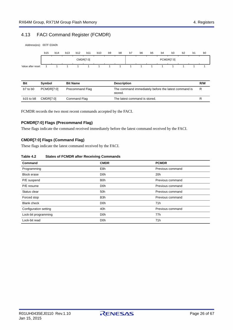
4.13 FACI Command Register (FCMDR)
FCMDR records the two most recent commands accepted by the FACI.
PCMDR[7:0] Flags (Precommand Flag)
These flags indicate the command received immediately before the latest command received by the FACI.
CMDR[7:0] Flags (Command Flag)
These flags indicate the latest command received by the FACI.
Address(es): 007F E0A0h
b15 b14 b13 b12 b11 b10 b9 b8 b7 b6 b5 b4 b3 b2 b1 b0
CMDR[7:0] PCMDR[7:0]
Value after reset: 1 1 1 1 1 1 1 1 1 1 1 1 1 1 1 1
Bit Symbol Bit Name Description R/W
b7 to b0 PCMDR[7:0] Precommand Flag The command immediately before the latest command is stored.
R
b15 to b8 CMDR[7:0] Command Flag The latest command is stored. R
Table 4.2 States of FCMDR after Receiving Commands
Command CMDR PCMDR
Programming E8h Previous command
Block erase D0h 20h
P/E suspend B0h Previous command
P/E resume D0h Previous command
Status clear 50h Previous command
Forced stop B3h Previous command
Blank check D0h 71h
Configuration setting 40h Previous command
Lock-bit programming D0h 77h
Lock-bit read D0h 71h
R01UH0435EJ0110 Rev.1.10 Page 27 of 67Jan 15, 2015
RX64M Group, RX71M Group Flash Memory 4. Registers
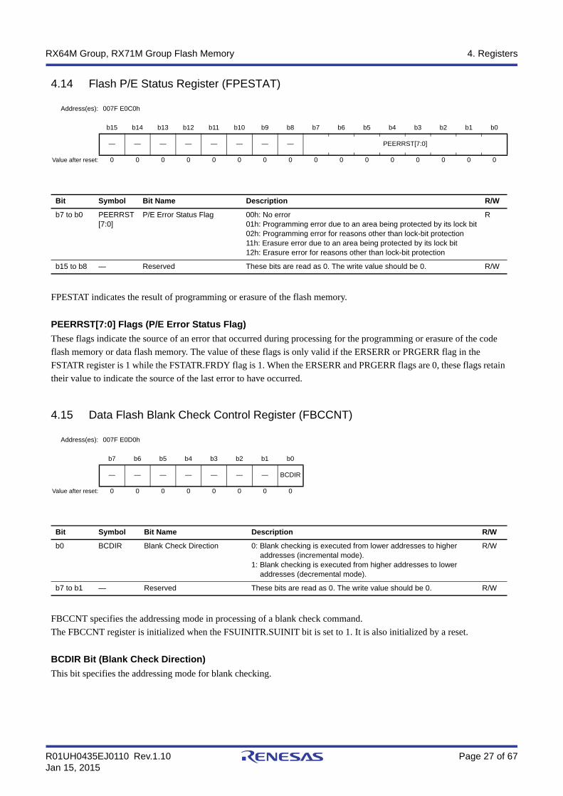
4.14 Flash P/E Status Register (FPESTAT)
FPESTAT indicates the result of programming or erasure of the flash memory.
PEERRST[7:0] Flags (P/E Error Status Flag)
These flags indicate the source of an error that occurred during processing for the programming or erasure of the code flash memory or data flash memory. The value of these flags is only valid if the ERSERR or PRGERR flag in the FSTATR register is 1 while the FSTATR.FRDY flag is 1. When the ERSERR and PRGERR flags are 0, these flags retain their value to indicate the source of the last error to have occurred.
4.15 Data Flash Blank Check Control Register (FBCCNT)
FBCCNT specifies the addressing mode in processing of a blank check command. The FBCCNT register is initialized when the FSUINITR.SUINIT bit is set to 1. It is also initialized by a reset.
BCDIR Bit (Blank Check Direction)
This bit specifies the addressing mode for blank checking.
Address(es): 007F E0C0h
b15 b14 b13 b12 b11 b10 b9 b8 b7 b6 b5 b4 b3 b2 b1 b0
— — — — — — — — PEERRST[7:0]
Value after reset: 0 0 0 0 0 0 0 0 0 0 0 0 0 0 0 0
Bit Symbol Bit Name Description R/W
b7 to b0 PEERRST[7:0]
P/E Error Status Flag 00h: No error01h: Programming error due to an area being protected by its lock bit02h: Programming error for reasons other than lock-bit protection11h: Erasure error due to an area being protected by its lock bit12h: Erasure error for reasons other than lock-bit protection
R
b15 to b8 — Reserved These bits are read as 0. The write value should be 0. R/W
Address(es): 007F E0D0h
b7 b6 b5 b4 b3 b2 b1 b0
— — — — — — — BCDIR
Value after reset: 0 0 0 0 0 0 0 0
Bit Symbol Bit Name Description R/W
b0 BCDIR Blank Check Direction 0: Blank checking is executed from lower addresses to higher addresses (incremental mode).
1: Blank checking is executed from higher addresses to lower addresses (decremental mode).
R/W
b7 to b1 — Reserved These bits are read as 0. The write value should be 0. R/W
R01UH0435EJ0110 Rev.1.10 Page 28 of 67Jan 15, 2015
RX64M Group, RX71M Group Flash Memory 4. Registers
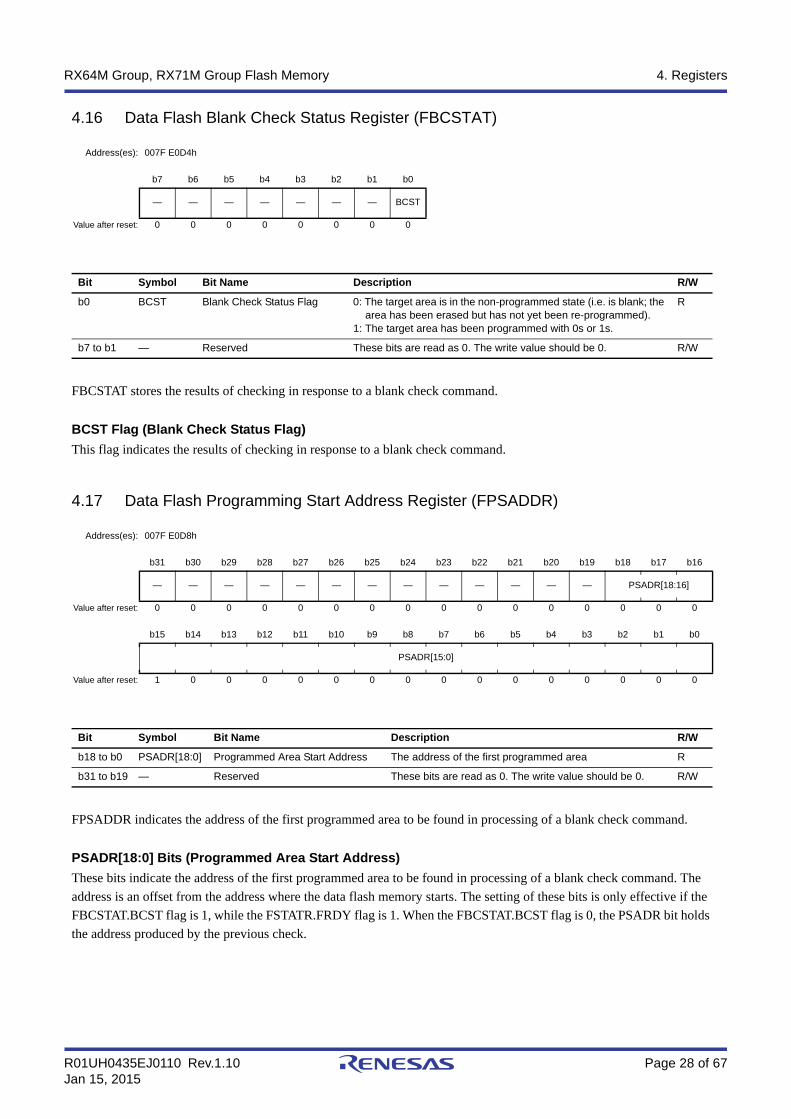
4.16 Data Flash Blank Check Status Register (FBCSTAT)
FBCSTAT stores the results of checking in response to a blank check command.
BCST Flag (Blank Check Status Flag)
This flag indicates the results of checking in response to a blank check command.
4.17 Data Flash Programming Start Address Register (FPSADDR)
FPSADDR indicates the address of the first programmed area to be found in processing of a blank check command.
PSADR[18:0] Bits (Programmed Area Start Address)
These bits indicate the address of the first programmed area to be found in processing of a blank check command. The address is an offset from the address where the data flash memory starts. The setting of these bits is only effective if the FBCSTAT.BCST flag is 1, while the FSTATR.FRDY flag is 1. When the FBCSTAT.BCST flag is 0, the PSADR bit holds the address produced by the previous check.
Address(es): 007F E0D4h
b7 b6 b5 b4 b3 b2 b1 b0
— — — — — — — BCST
Value after reset: 0 0 0 0 0 0 0 0
Bit Symbol Bit Name Description R/W
b0 BCST Blank Check Status Flag 0: The target area is in the non-programmed state (i.e. is blank; the area has been erased but has not yet been re-programmed).
1: The target area has been programmed with 0s or 1s.
R
b7 to b1 — Reserved These bits are read as 0. The write value should be 0. R/W
Address(es): 007F E0D8h
b31 b30 b29 b28 b27 b26 b25 b24 b23 b22 b21 b20 b19 b18 b17 b16
— — — — — — — — — — — — — PSADR[18:16]
Value after reset: 0 0 0 0 0 0 0 0 0 0 0 0 0 0 0 0
b15 b14 b13 b12 b11 b10 b9 b8 b7 b6 b5 b4 b3 b2 b1 b0
PSADR[15:0]
Value after reset: 1 0 0 0 0 0 0 0 0 0 0 0 0 0 0 0
Bit Symbol Bit Name Description R/W
b18 to b0 PSADR[18:0] Programmed Area Start Address The address of the first programmed area R
b31 to b19 — Reserved These bits are read as 0. The write value should be 0. R/W
R01UH0435EJ0110 Rev.1.10 Page 29 of 67Jan 15, 2015
RX64M Group, RX71M Group Flash Memory 4. Registers
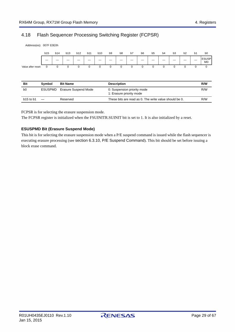
4.18 Flash Sequencer Processing Switching Register (FCPSR)
FCPSR is for selecting the erasure suspension mode. The FCPSR register is initialized when the FSUINITR.SUINIT bit is set to 1. It is also initialized by a reset.
ESUSPMD Bit (Erasure Suspend Mode)
This bit is for selecting the erasure suspension mode when a P/E suspend command is issued while the flash sequencer is executing erasure processing (see section 6.3.10, P/E Suspend Command). This bit should be set before issuing a block erase command.
Address(es): 007F E0E0h
b15 b14 b13 b12 b11 b10 b9 b8 b7 b6 b5 b4 b3 b2 b1 b0
— — — — — — — — — — — — — — — ESUSPMD
Value after reset: 0 0 0 0 0 0 0 0 0 0 0 0 0 0 0 0
Bit Symbol Bit Name Description R/W
b0 ESUSPMD Erasure Suspend Mode 0: Suspension priority mode1: Erasure priority mode
R/W
b15 to b1 — Reserved These bits are read as 0. The write value should be 0. R/W
R01UH0435EJ0110 Rev.1.10 Page 30 of 67Jan 15, 2015
RX64M Group, RX71M Group Flash Memory 4. Registers
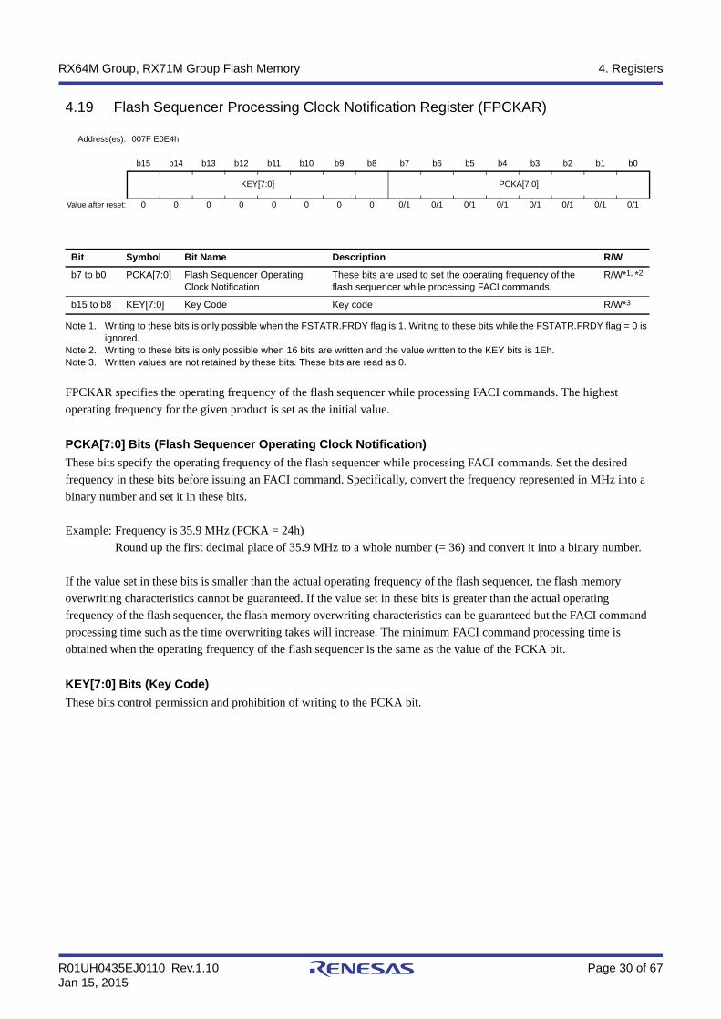
4.19 Flash Sequencer Processing Clock Notification Register (FPCKAR)
Note 1. Writing to these bits is only possible when the FSTATR.FRDY flag is 1. Writing to these bits while the FSTATR.FRDY flag = 0 is ignored.
Note 2. Writing to these bits is only possible when 16 bits are written and the value written to the KEY bits is 1Eh.Note 3. Written values are not retained by these bits. These bits are read as 0.
FPCKAR specifies the operating frequency of the flash sequencer while processing FACI commands. The highest operating frequency for the given product is set as the initial value.
PCKA[7:0] Bits (Flash Sequencer Operating Clock Notification)
These bits specify the operating frequency of the flash sequencer while processing FACI commands. Set the desired frequency in these bits before issuing an FACI command. Specifically, convert the frequency represented in MHz into a binary number and set it in these bits.
Example: Frequency is 35.9 MHz (PCKA = 24h)Round up the first decimal place of 35.9 MHz to a whole number (= 36) and convert it into a binary number.
If the value set in these bits is smaller than the actual operating frequency of the flash sequencer, the flash memory overwriting characteristics cannot be guaranteed. If the value set in these bits is greater than the actual operating frequency of the flash sequencer, the flash memory overwriting characteristics can be guaranteed but the FACI command processing time such as the time overwriting takes will increase. The minimum FACI command processing time is obtained when the operating frequency of the flash sequencer is the same as the value of the PCKA bit.
KEY[7:0] Bits (Key Code)
These bits control permission and prohibition of writing to the PCKA bit.
Address(es): 007F E0E4h
b15 b14 b13 b12 b11 b10 b9 b8 b7 b6 b5 b4 b3 b2 b1 b0
KEY[7:0] PCKA[7:0]
Value after reset: 0 0 0 0 0 0 0 0 0/1 0/1 0/1 0/1 0/1 0/1 0/1 0/1
Bit Symbol Bit Name Description R/W
b7 to b0 PCKA[7:0] Flash Sequencer Operating Clock Notification
These bits are used to set the operating frequency of the flash sequencer while processing FACI commands.
R/W*1, *2
b15 to b8 KEY[7:0] Key Code Key code R/W*3
R01UH0435EJ0110 Rev.1.10 Page 31 of 67Jan 15, 2015
RX64M Group, RX71M Group Flash Memory 5. Operating Modes of the Flash Sequencer
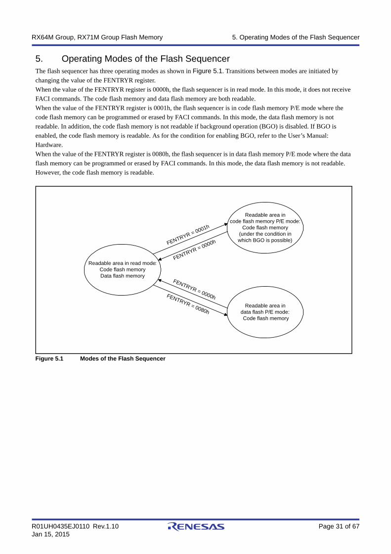
5. Operating Modes of the Flash SequencerThe flash sequencer has three operating modes as shown in Figure 5.1. Transitions between modes are initiated by changing the value of the FENTRYR register.When the value of the FENTRYR register is 0000h, the flash sequencer is in read mode. In this mode, it does not receive FACI commands. The code flash memory and data flash memory are both readable.When the value of the FENTRYR register is 0001h, the flash sequencer is in code flash memory P/E mode where the code flash memory can be programmed or erased by FACI commands. In this mode, the data flash memory is not readable. In addition, the code flash memory is not readable if background operation (BGO) is disabled. If BGO is enabled, the code flash memory is readable. As for the condition for enabling BGO, refer to the User’s Manual: Hardware.When the value of the FENTRYR register is 0080h, the flash sequencer is in data flash memory P/E mode where the data flash memory can be programmed or erased by FACI commands. In this mode, the data flash memory is not readable. However, the code flash memory is readable.
Figure 5.1 Modes of the Flash Sequencer
Readable area in code flash memory P/E mode:
Code flash memory(under the condition in which BGO is possible)
Readable area in data flash P/E mode: Code flash memory
FENTRYR = 0080h
FENTRYR = 0000h
FENTRYR = 0001h
FENTRYR = 0000h
Readable area in read mode:Code flash memoryData flash memory
R01UH0435EJ0110 Rev.1.10 Page 32 of 67Jan 15, 2015
RX64M Group, RX71M Group Flash Memory 6. FACI Commands
6. FACI Commands
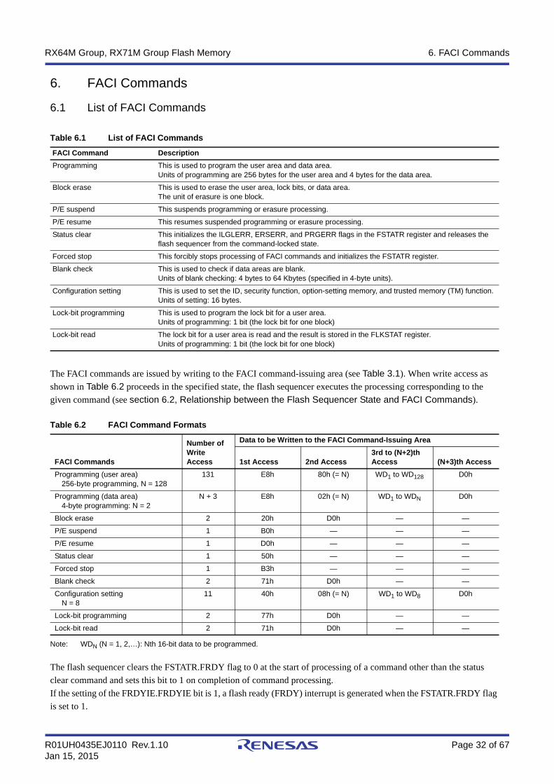
6.1 List of FACI Commands
The FACI commands are issued by writing to the FACI command-issuing area (see Table 3.1). When write access as shown in Table 6.2 proceeds in the specified state, the flash sequencer executes the processing corresponding to the given command (see section 6.2, Relationship between the Flash Sequencer State and FACI Commands).
Note: WDN (N = 1, 2,…): Nth 16-bit data to be programmed.
The flash sequencer clears the FSTATR.FRDY flag to 0 at the start of processing of a command other than the status clear command and sets this bit to 1 on completion of command processing. If the setting of the FRDYIE.FRDYIE bit is 1, a flash ready (FRDY) interrupt is generated when the FSTATR.FRDY flag is set to 1.
Table 6.1 List of FACI Commands
FACI Command Description
Programming This is used to program the user area and data area.Units of programming are 256 bytes for the user area and 4 bytes for the data area.
Block erase This is used to erase the user area, lock bits, or data area.The unit of erasure is one block.
P/E suspend This suspends programming or erasure processing.
P/E resume This resumes suspended programming or erasure processing.
Status clear This initializes the ILGLERR, ERSERR, and PRGERR flags in the FSTATR register and releases the flash sequencer from the command-locked state.
Forced stop This forcibly stops processing of FACI commands and initializes the FSTATR register.
Blank check This is used to check if data areas are blank.Units of blank checking: 4 bytes to 64 Kbytes (specified in 4-byte units).
Configuration setting This is used to set the ID, security function, option-setting memory, and trusted memory (TM) function.Units of setting: 16 bytes.
Lock-bit programming This is used to program the lock bit for a user area.Units of programming: 1 bit (the lock bit for one block)
Lock-bit read The lock bit for a user area is read and the result is stored in the FLKSTAT register.Units of programming: 1 bit (the lock bit for one block)
Table 6.2 FACI Command Formats
FACI Commands
Number of Write Access
Data to be Written to the FACI Command-Issuing Area
1st Access 2nd Access3rd to (N+2)th Access (N+3)th Access
Programming (user area)256-byte programming, N = 128
131 E8h 80h (= N) WD1 to WD128 D0h
Programming (data area)4-byte programming: N = 2
N + 3 E8h 02h (= N) WD1 to WDN D0h
Block erase 2 20h D0h — —
P/E suspend 1 B0h — — —
P/E resume 1 D0h — — —
Status clear 1 50h — — —
Forced stop 1 B3h — — —
Blank check 2 71h D0h — —
Configuration settingN = 8
11 40h 08h (= N) WD1 to WD8 D0h
Lock-bit programming 2 77h D0h — —
Lock-bit read 2 71h D0h — —
R01UH0435EJ0110 Rev.1.10 Page 33 of 67Jan 15, 2015
RX64M Group, RX71M Group Flash Memory 6. FACI Commands
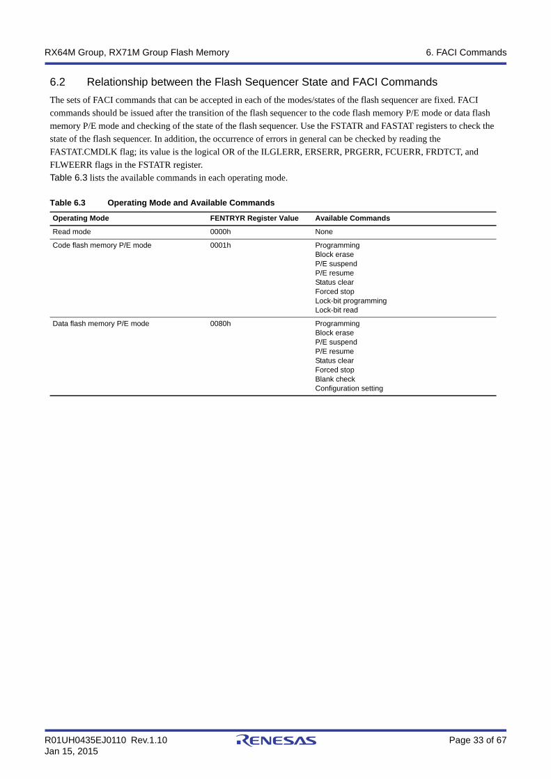
6.2 Relationship between the Flash Sequencer State and FACI Commands
The sets of FACI commands that can be accepted in each of the modes/states of the flash sequencer are fixed. FACI commands should be issued after the transition of the flash sequencer to the code flash memory P/E mode or data flash memory P/E mode and checking of the state of the flash sequencer. Use the FSTATR and FASTAT registers to check the state of the flash sequencer. In addition, the occurrence of errors in general can be checked by reading the FASTAT.CMDLK flag; its value is the logical OR of the ILGLERR, ERSERR, PRGERR, FCUERR, FRDTCT, and FLWEERR flags in the FSTATR register.Table 6.3 lists the available commands in each operating mode.
Table 6.3 Operating Mode and Available Commands
Operating Mode FENTRYR Register Value Available Commands
Read mode 0000h None
Code flash memory P/E mode 0001h ProgrammingBlock eraseP/E suspendP/E resumeStatus clearForced stopLock-bit programmingLock-bit read
Data flash memory P/E mode 0080h ProgrammingBlock eraseP/E suspendP/E resumeStatus clearForced stopBlank checkConfiguration setting
R01UH0435EJ0110 Rev.1.10 Page 34 of 67Jan 15, 2015
RX64M Group, RX71M Group Flash Memory 6. FACI Commands
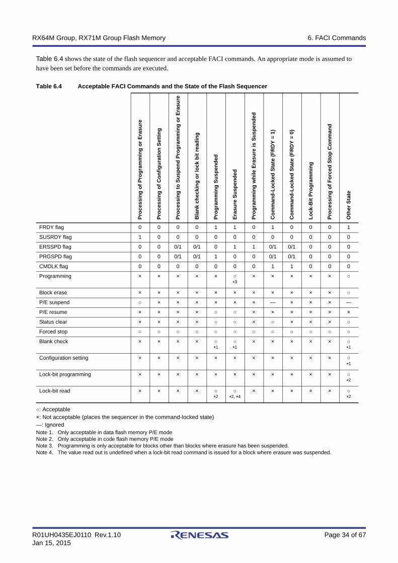
Table 6.4 shows the state of the flash sequencer and acceptable FACI commands. An appropriate mode is assumed to have been set before the commands are executed.
○: Acceptable×: Not acceptable (places the sequencer in the command-locked state)—: IgnoredNote 1. Only acceptable in data flash memory P/E modeNote 2. Only acceptable in code flash memory P/E modeNote 3. Programming is only acceptable for blocks other than blocks where erasure has been suspended.Note 4. The value read out is undefined when a lock-bit read command is issued for a block where erasure was suspended.
Table 6.4 Acceptable FACI Commands and the State of the Flash Sequencer
Pro
ces
sin
g o
f P
rog
ram
min
g o
r E
rasu
re
Pro
ces
sin
g o
f C
on
fig
ura
tio
n S
etti
ng
Pro
ces
sin
g t
o S
usp
en
d P
rog
ram
min
g o
r E
rasu
re
Bla
nk
chec
kin
g o
r lo
ck b
it r
ead
ing
Pro
gra
mm
ing
Su
spen
ded
Era
sure
Su
spe
nd
ed
Pro
gra
mm
ing
wh
ile E
rasu
re is
Su
spe
nd
ed
Co
mm
and
-Lo
cked
Sta
te (
FR
DY
= 1
)
Co
mm
and
-Lo
cked
Sta
te (
FR
DY
= 0
)
Lo
ck-B
it P
rog
ram
min
g
Pro
ces
sin
g o
f F
orc
ed
Sto
p C
om
man
d
Oth
er
Sta
te
FRDY flag 0 0 0 0 1 1 0 1 0 0 0 1
SUSRDY flag 1 0 0 0 0 0 0 0 0 0 0 0
ERSSPD flag 0 0 0/1 0/1 0 1 1 0/1 0/1 0 0 0
PRGSPD flag 0 0 0/1 0/1 1 0 0 0/1 0/1 0 0 0
CMDLK flag 0 0 0 0 0 0 0 1 1 0 0 0
Programming × × × × × ○*3
× × × × × ○
Block erase × × × × × × × × × × × ○
P/E suspend ○ × × × × × × — × × × —
P/E resume × × × × ○ ○ × × × × × ×
Status clear × × × × ○ ○ × ○ × × × ○
Forced stop ○ ○ ○ ○ ○ ○ ○ ○ ○ ○ ○ ○
Blank check × × × × ○*1
○*1
× × × × × ○*1
Configuration setting × × × × × × × × × × × ○*1
Lock-bit programming × × × × × × × × × × × ○*2
Lock-bit read × × × × ○*2
○*2, *4
× × × × × ○*2
R01UH0435EJ0110 Rev.1.10 Page 35 of 67Jan 15, 2015
RX64M Group, RX71M Group Flash Memory 6. FACI Commands
6.3 Usage of FACI Commands
This section gives an overview of the usage of FACI commands.
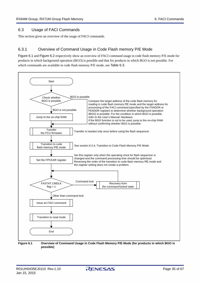
6.3.1 Overview of Command Usage in Code Flash memory P/E Mode
Figure 6.1 and Figure 6.2 respectively show an overview of FACI command usage in code flash memory P/E mode for products in which background operation (BGO) is possible and that for products in which BGO is not possible. For which commands are available in code flash memory P/E mode, see Table 6.3.
Figure 6.1 Overview of Command Usage in Code Flash Memory P/E Mode (for products in which BGO is possible)
Set this register only when the operating clock for flash sequencer is changed and the command processing time should be optimized.Reversing the order of the transition to code flash memory P/E mode and the register setting does not create a problem.
Transfer the FCU firmware
Start
Check whether BGO is possible
Jump to the on-chip RAM
BGO is possible
BGO is not possible
Transition to code flash memory P/E mode
Set the FPCKAR register
Transfer is needed only once before using the flash sequencer.
FASTAT.CMDLKflag = 1
Recovery from the command-locked state
Command lock
Other than command lock
Issue an FACI command
Transition to read mode
End
Compare the target address of the code flash memory for reading in code flash memory P/E mode and the target address for processing of the FACI command (specified by the FSADDR or FEADDR register) to determine whether background operation (BGO) is possible. For the condition in which BGO is possible, refer to the User’s Manual: Hardware.If the BGO function is not to be used, jump to the on-chip RAM without confirming whether BGO is possible.
See section 6.3.4, Transition to Code Flash Memory P/E Mode.
R01UH0435EJ0110 Rev.1.10 Page 36 of 67Jan 15, 2015
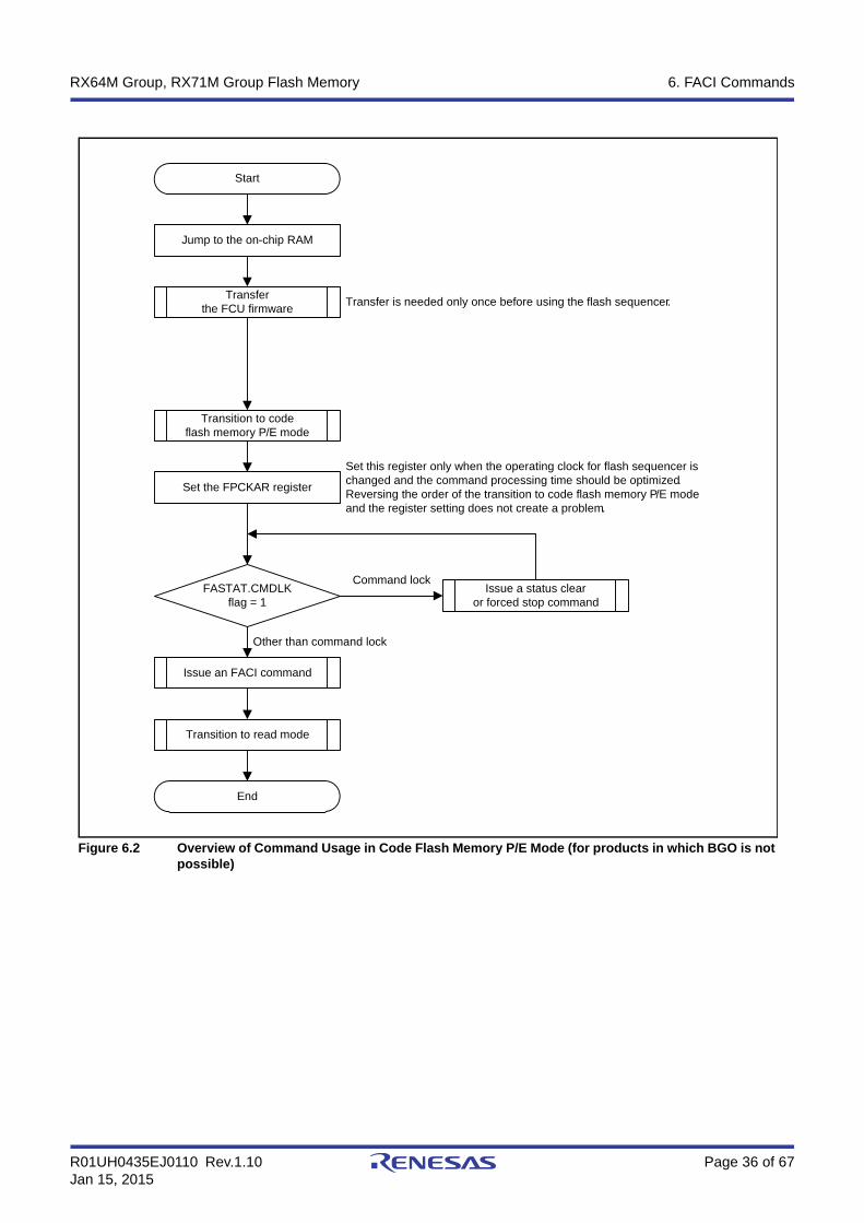
RX64M Group, RX71M Group Flash Memory 6. FACI Commands
Figure 6.2 Overview of Command Usage in Code Flash Memory P/E Mode (for products in which BGO is not possible)
Set this register only when the operating clock for flash sequencer ischanged and the command processing time should be optimized.Reversing the order of the transition to code flash memory P/E mode and the register setting does not create a problem.
Transferthe FCU firmware
Start
Jump to the on-chip RAM
Transition to code flash memory P/E mode
Set the FPCKAR register
Transfer is needed only once before using the flash sequencer.
FASTAT.CMDLKflag = 1
Issue a status clearor forced stop command
Command lock
Other than command lock
Issue an FACI command
Transition to read mode
End
R01UH0435EJ0110 Rev.1.10 Page 37 of 67Jan 15, 2015
RX64M Group, RX71M Group Flash Memory 6. FACI Commands
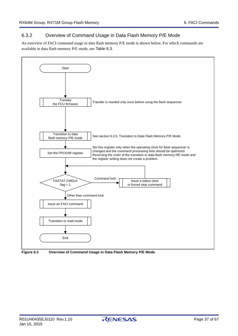
6.3.2 Overview of Command Usage in Data Flash Memory P/E Mode
An overview of FACI command usage in data flash memory P/E mode is shown below. For which commands are available in data flash memory P/E mode, see Table 6.3.
Figure 6.3 Overview of Command Usage in Data Flash Memory P/E Mode
Set this register only when the operating clock for flash sequencer ischanged and the command processing time should be optimized.Reversing the order of the transition to data flash memory P/E mode and the register setting does not create a problem.
Transferthe FCU firmware
Start
Transition to data flash memory P/E mode
Set the FPCKAR register
Transfer is needed only once before using the flash sequencer.
FASTAT.CMDLKflag = 1
Issue a status clearor forced stop command
Command lock
Other than command lock
Issue an FACI command
Transition to read mode
End
See section 6.3.5, Transition to Data Flash Memory P/E Mode.
R01UH0435EJ0110 Rev.1.10 Page 38 of 67Jan 15, 2015
RX64M Group, RX71M Group Flash Memory 6. FACI Commands
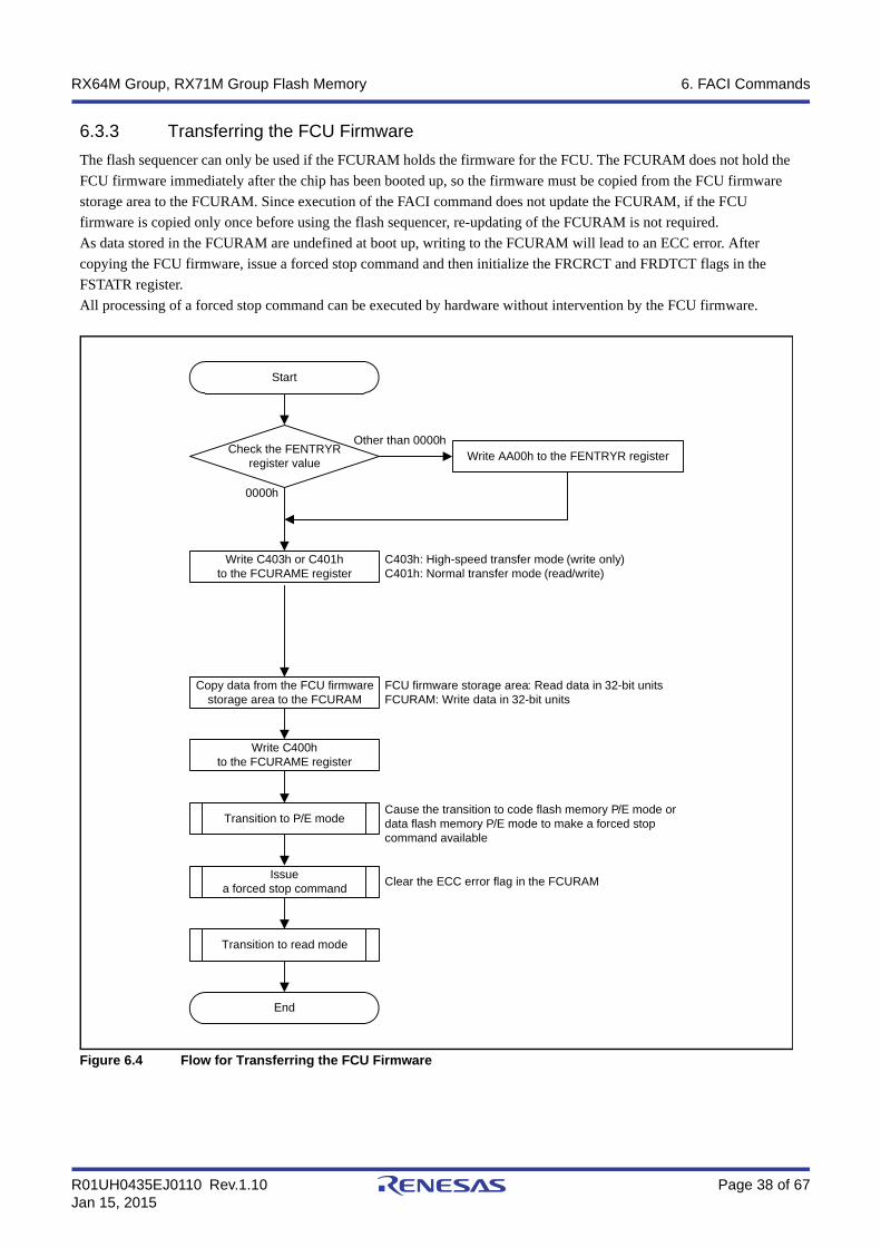
6.3.3 Transferring the FCU Firmware
The flash sequencer can only be used if the FCURAM holds the firmware for the FCU. The FCURAM does not hold the FCU firmware immediately after the chip has been booted up, so the firmware must be copied from the FCU firmware storage area to the FCURAM. Since execution of the FACI command does not update the FCURAM, if the FCU firmware is copied only once before using the flash sequencer, re-updating of the FCURAM is not required.As data stored in the FCURAM are undefined at boot up, writing to the FCURAM will lead to an ECC error. After copying the FCU firmware, issue a forced stop command and then initialize the FRCRCT and FRDTCT flags in the FSTATR register.All processing of a forced stop command can be executed by hardware without intervention by the FCU firmware.
Figure 6.4 Flow for Transferring the FCU Firmware
FCU firmware storage area: Read data in 32-bit unitsFCURAM: Write data in 32-bit units
Start
Write C403h or C401hto the FCURAME register
C403h: High-speed transfer mode (write only)C401h: Normal transfer mode (read/write)
Check the FENTRYR register value
Other than 0000h
0000h
Issuea forced stop command
Transition to read mode
End
Write AA00h to the FENTRYR register
Transition to P/E mode
Copy data from the FCU firmwarestorage area to the FCURAM
Write C400hto the FCURAME register
Cause the transition to code flash memory P/E mode or data flash memory P/E mode to make a forced stop command available
Clear the ECC error flag in the FCURAM
R01UH0435EJ0110 Rev.1.10 Page 39 of 67Jan 15, 2015
RX64M Group, RX71M Group Flash Memory 6. FACI Commands
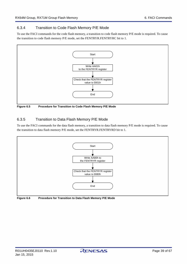
6.3.4 Transition to Code Flash Memory P/E Mode
To use the FACI commands for the code flash memory, a transition to code flash memory P/E mode is required. To cause the transition to code flash memory P/E mode, set the FENTRYR.FENTRYRC bit to 1.
Figure 6.5 Procedure for Transition to Code Flash Memory P/E Mode
6.3.5 Transition to Data Flash Memory P/E Mode
To use the FACI commands for the data flash memory, a transition to data flash memory P/E mode is required. To cause the transition to data flash memory P/E mode, set the FENTRYR.FENTRYRD bit to 1.
Figure 6.6 Procedure for Transition to Data Flash Memory P/E Mode
Start
End
Check that the FENTRYR registervalue is 0001h
Write AA01hto the FENTRYR register
Start
End
Check that the FENTRYR registervalue is 0080h
Write AA80h tothe FENTRYR register
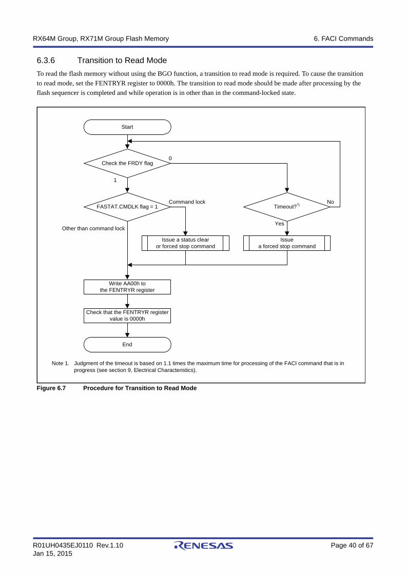
R01UH0435EJ0110 Rev.1.10 Page 40 of 67Jan 15, 2015
RX64M Group, RX71M Group Flash Memory 6. FACI Commands
6.3.6 Transition to Read Mode
To read the flash memory without using the BGO function, a transition to read mode is required. To cause the transition to read mode, set the FENTRYR register to 0000h. The transition to read mode should be made after processing by the flash sequencer is completed and while operation is in other than in the command-locked state.
Figure 6.7 Procedure for Transition to Read Mode
Start
Check the FRDY flag0
1
Issuea forced stop command
End
Issue a status clearor forced stop command
Write AA00h tothe FENTRYR register
Check that the FENTRYR registervalue is 0000h
FASTAT.CMDLK flag = 1Command lock
Other than command lock
Timeout?*1No
Yes
Note 1. Judgment of the timeout is based on 1.1 times the maximum time for processing of the FACI command that is in progress (see section 9, Electrical Characteristics).
R01UH0435EJ0110 Rev.1.10 Page 41 of 67Jan 15, 2015
RX64M Group, RX71M Group Flash Memory 6. FACI Commands
6.3.7 Recovery from the Command-Locked State
When the flash sequencer enters the command-locked state, FACI commands cannot be accepted. To release the sequencer from the command-locked state, use the status clear command, forced stop command, or FASTAT register.When the command-locked state is detected by checking for an error before issuing the P/E suspend command, the FSTATR.FRDY flag may hold 0 although command processing has not been completed. If processing is not completed within the maximum programming/erasure time specified in the User's Manual: Hardware, this can be considered a timeout, and the flash sequencer should be stopped by the forced stop command.When the FSTATR.ILGLERR flag is 1, check the FASTAT value. If the CFAE or DFAE flag in the FASTAT register is 1, the status clear and forced stop commands cannot be used to release the sequencer from the command-locked state.The FCUERR, FRDTCT, and FLWERR flags in the FSTATR register are not changed from 1 to 0 by the status clear command. When these bits are set to 1, use the forced stop command for release from the command-locked state. The other bits that indicate the command-locked state can be changed from 1 to 0 by the status clear or forced stop command.
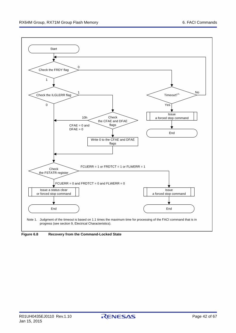
R01UH0435EJ0110 Rev.1.10 Page 42 of 67Jan 15, 2015
RX64M Group, RX71M Group Flash Memory 6. FACI Commands
Figure 6.8 Recovery from the Command-Locked State
Note 1. Judgment of the timeout is based on 1.1 times the maximum time for processing of the FACI command that is in progress (see section 9, Electrical Characteristics).
Start
Check the FRDY flag0
1
Issuea forced stop command
End
Check the ILGLERR flag1
0
Timeout?*1No
Yes
Issue a status clearor forced stop command
Checkthe CFAE and DFAE
flags
Write 0 to the CFAE and DFAE flags
Check the FSTATR register
End
Issuea forced stop command
End
FCUERR = 1 or FRDTCT = 1 or FLWERR = 1
FCUERR = 0 and FRDTCT = 0 and FLWERR = 0
10h
CFAE = 0 and DFAE = 0
R01UH0435EJ0110 Rev.1.10 Page 43 of 67Jan 15, 2015
RX64M Group, RX71M Group Flash Memory 6. FACI Commands
6.3.8 Programming Command
A programming command is used for writing to the user area and data area.Before issuing a programming command, set the first address of the target block in the FSADDR register.Writing D0h to the FACI command-issuing area at the final access of the FACI command-issuing starts the programming command processing. If the target area of programming command processing contains the area not for writing, write FFFFh to the corresponding area.The FPROTR register must be set before issuing a programming command. To switch between enabling and disabling of the lock bits, the setting of the FPROTR register must be changed.Issuing a programming command while the FACI internal data buffer is full leads to a wait on the peripheral bus 6, and this may affect the communications performance of other peripheral IP modules. To avoid the generation of a wait in this way, the FSTATR.DBFULL flag should be 0 when an FACI command is issued.Writing to the data area will not lead to the data buffer becoming full.
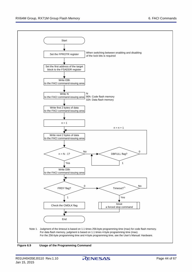
R01UH0435EJ0110 Rev.1.10 Page 44 of 67Jan 15, 2015
RX64M Group, RX71M Group Flash Memory 6. FACI Commands
Figure 6.9 Usage of the Programming Command
Start
Issuea forced stop command
End
Check the CMDLK flag
n = N - 1?
Timeout?*1No
Yes
DBFULL flag?0
1
Set the FPROTR registerWhen switching between enabling and disablingof the lock bits is required
Set the first address of the target block to the FSADDR register
Write E8hto the FACI command-issuing area
Write Nto the FACI command-issuing area
N80h: Code flash memory02h: Data flash memory
Write first 2 bytes of datato the FACI command-issuing area
n = 1
Write next 2 bytes of datato the FACI command-issuing area
Write D0hto the FACI command-issuing area
FRDY flag?
No
Yes
n = n + 1
0
1
Note 1. Judgment of the timeout is based on 1.1 times 256-byte programming time (max) for code flash memory. For data flash memory, judgment is based on 1.1 times 4-byte programming time (max).For the 256-byte programming time and 4-byte programming time, see the User’s Manual: Hardware.
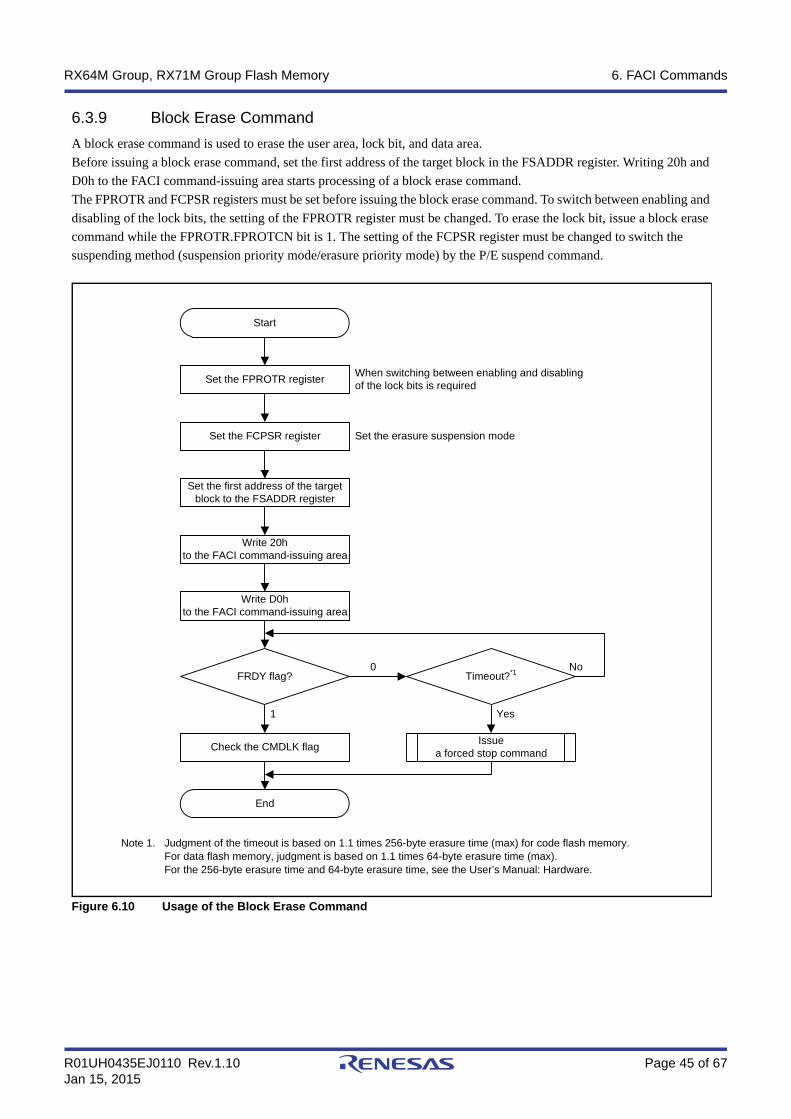
R01UH0435EJ0110 Rev.1.10 Page 45 of 67Jan 15, 2015
RX64M Group, RX71M Group Flash Memory 6. FACI Commands
6.3.9 Block Erase Command
A block erase command is used to erase the user area, lock bit, and data area.Before issuing a block erase command, set the first address of the target block in the FSADDR register. Writing 20h and D0h to the FACI command-issuing area starts processing of a block erase command.The FPROTR and FCPSR registers must be set before issuing the block erase command. To switch between enabling and disabling of the lock bits, the setting of the FPROTR register must be changed. To erase the lock bit, issue a block erase command while the FPROTR.FPROTCN bit is 1. The setting of the FCPSR register must be changed to switch the suspending method (suspension priority mode/erasure priority mode) by the P/E suspend command.
Figure 6.10 Usage of the Block Erase Command
Start
Issuea forced stop command
End
Check the CMDLK flag
Timeout?*1No
Yes
Set the FPROTR registerWhen switching between enabling and disablingof the lock bits is required
Set the FCPSR register
Set the first address of the target block to the FSADDR register
Write 20hto the FACI command-issuing area
Write D0hto the FACI command-issuing area
FRDY flag?0
1
Set the erasure suspension mode
Note 1. Judgment of the timeout is based on 1.1 times 256-byte erasure time (max) for code flash memory. For data flash memory, judgment is based on 1.1 times 64-byte erasure time (max).For the 256-byte erasure time and 64-byte erasure time, see the User’s Manual: Hardware.
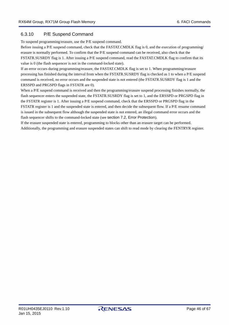
R01UH0435EJ0110 Rev.1.10 Page 46 of 67Jan 15, 2015
RX64M Group, RX71M Group Flash Memory 6. FACI Commands
6.3.10 P/E Suspend Command
To suspend programming/erasure, use the P/E suspend command.Before issuing a P/E suspend command, check that the FASTAT.CMDLK flag is 0, and the execution of programming/erasure is normally performed. To confirm that the P/E suspend command can be received, also check that the FSTATR.SUSRDY flag is 1. After issuing a P/E suspend command, read the FASTAT.CMDLK flag to confirm that its value is 0 (the flash sequencer is not in the command-locked state).If an error occurs during programming/erasure, the FASTAT.CMDLK flag is set to 1. When programming/erasure processing has finished during the interval from when the FSTATR.SUSRDY flag is checked as 1 to when a P/E suspend command is received, no error occurs and the suspended state is not entered (the FSTATR.SUSRDY flag is 1 and the ERSSPD and PRGSPD flags in FSTATR are 0).When a P/E suspend command is received and then the programming/erasure suspend processing finishes normally, the flash sequencer enters the suspended state, the FSTATR.SUSRDY flag is set to 1, and the ERSSPD or PRGSPD flag in the FSTATR register is 1. After issuing a P/E suspend command, check that the ERSSPD or PRGSPD flag in the FSTATR register is 1 and the suspended state is entered, and then decide the subsequent flow. If a P/E resume command is issued in the subsequent flow although the suspended state is not entered, an illegal command error occurs and the flash sequencer shifts to the command-locked state (see section 7.2, Error Protection).If the erasure suspended state is entered, programming to blocks other than an erasure target can be performed. Additionally, the programming and erasure suspended states can shift to read mode by clearing the FENTRYR register.
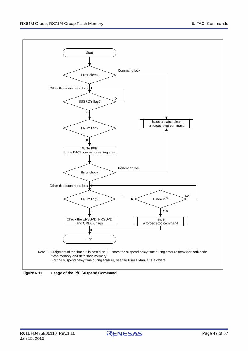
R01UH0435EJ0110 Rev.1.10 Page 47 of 67Jan 15, 2015
RX64M Group, RX71M Group Flash Memory 6. FACI Commands
Figure 6.11 Usage of the P/E Suspend Command
Start
Issuea forced stop command
End
Check the ERSSPD, PRGSPDand CMDLK flags
Timeout?*1No
Yes
FRDY flag?0
1
Error check
SUSRDY flag?
Other than command lock
Command lock
0
1
FRDY flag?
0
Write B0hto the FACI command-issuing area
Error check
Other than command lock
Command lock
Issue a status clearor forced stop command
Note 1. Judgment of the timeout is based on 1.1 times the suspend delay time during erasure (max) for both code flash memory and data flash memory.For the suspend delay time during erasure, see the User’s Manual: Hardware.
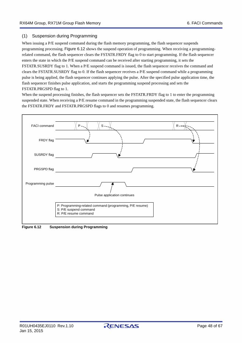
R01UH0435EJ0110 Rev.1.10 Page 48 of 67Jan 15, 2015
RX64M Group, RX71M Group Flash Memory 6. FACI Commands
(1) Suspension during Programming
When issuing a P/E suspend command during the flash memory programming, the flash sequencer suspends programming processing. Figure 6.12 shows the suspend operation of programming. When receiving a programming-related command, the flash sequencer clears the FSTATR.FRDY flag to 0 to start programming. If the flash sequencer enters the state in which the P/E suspend command can be received after starting programming, it sets the FSTATR.SUSRDY flag to 1. When a P/E suspend command is issued, the flash sequencer receives the command and clears the FSTATR.SUSRDY flag to 0. If the flash sequencer receives a P/E suspend command while a programming pulse is being applied, the flash sequencer continues applying the pulse. After the specified pulse application time, the flash sequencer finishes pulse application, and starts the programming suspend processing and sets the FSTATR.PRGSPD flag to 1.When the suspend processing finishes, the flash sequencer sets the FSTATR.FRDY flag to 1 to enter the programming suspended state. When receiving a P/E resume command in the programming suspended state, the flash sequencer clears the FSTATR.FRDY and FSTATR.PRGSPD flags to 0 and resumes programming.
Figure 6.12 Suspension during Programming
FACI command
P: Programming-related command (programming, P/E resume)S: P/E suspend commandR: P/E resume command
Pulse application continues
P S R
FRDY flag
SUSRDY flag
PRGSPD flag
Programming pulse
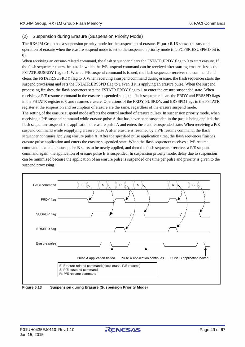
R01UH0435EJ0110 Rev.1.10 Page 49 of 67Jan 15, 2015
RX64M Group, RX71M Group Flash Memory 6. FACI Commands
(2) Suspension during Erasure (Suspension Priority Mode)
The RX64M Group has a suspension priority mode for the suspension of erasure. Figure 6.13 shows the suspend operation of erasure when the erasure suspend mode is set to the suspension priority mode (the FCPSR.ESUSPMD bit is 0).When receiving an erasure-related command, the flash sequencer clears the FSTATR.FRDY flag to 0 to start erasure. If the flash sequencer enters the state in which the P/E suspend command can be received after starting erasure, it sets the FSTATR.SUSRDY flag to 1. When a P/E suspend command is issued, the flash sequencer receives the command and clears the FSTATR.SUSRDY flag to 0. When receiving a suspend command during erasure, the flash sequencer starts the suspend processing and sets the FSTATR.ERSSPD flag to 1 even if it is applying an erasure pulse. When the suspend processing finishes, the flash sequencer sets the FSTATR.FRDY flag to 1 to enter the erasure suspended state. When receiving a P/E resume command in the erasure suspended state, the flash sequencer clears the FRDY and ERSSPD flags in the FSTATR register to 0 and resumes erasure. Operations of the FRDY, SUSRDY, and ERSSPD flags in the FSTATR register at the suspension and resumption of erasure are the same, regardless of the erasure suspend mode.The setting of the erasure suspend mode affects the control method of erasure pulses. In suspension priority mode, when receiving a P/E suspend command while erasure pulse A that has never been suspended in the past is being applied, the flash sequencer suspends the application of erasure pulse A and enters the erasure suspended state. When receiving a P/E suspend command while reapplying erasure pulse A after erasure is resumed by a P/E resume command, the flash sequencer continues applying erasure pulse A. After the specified pulse application time, the flash sequencer finishes erasure pulse application and enters the erasure suspended state. When the flash sequencer receives a P/E resume command next and erasure pulse B starts to be newly applied, and then the flash sequencer receives a P/E suspend command again, the application of erasure pulse B is suspended. In suspension priority mode, delay due to suspension can be minimized because the application of an erasure pulse is suspended one time per pulse and priority is given to the suspend processing.
Figure 6.13 Suspension during Erasure (Suspension Priority Mode)
SFACI command
E: Erasure-related command (block erase, P/E resume)S: P/E suspend commandR: P/E resume command
Pulse A application halted
E S R
FRDY flag
SUSRDY flag
ERSSPD flag
Erasure pulse
R S
Pulse A application continues Pulse B application halted
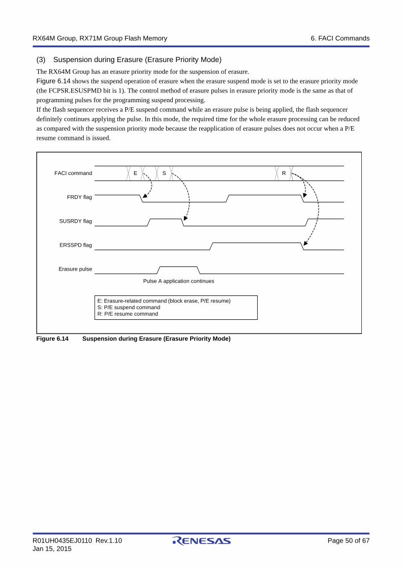
R01UH0435EJ0110 Rev.1.10 Page 50 of 67Jan 15, 2015
RX64M Group, RX71M Group Flash Memory 6. FACI Commands
(3) Suspension during Erasure (Erasure Priority Mode)
The RX64M Group has an erasure priority mode for the suspension of erasure.Figure 6.14 shows the suspend operation of erasure when the erasure suspend mode is set to the erasure priority mode (the FCPSR.ESUSPMD bit is 1). The control method of erasure pulses in erasure priority mode is the same as that of programming pulses for the programming suspend processing.If the flash sequencer receives a P/E suspend command while an erasure pulse is being applied, the flash sequencer definitely continues applying the pulse. In this mode, the required time for the whole erasure processing can be reduced as compared with the suspension priority mode because the reapplication of erasure pulses does not occur when a P/E resume command is issued.
Figure 6.14 Suspension during Erasure (Erasure Priority Mode)
FACI command
E: Erasure-related command (block erase, P/E resume)S: P/E suspend commandR: P/E resume command
E S R
FRDY flag
SUSRDY flag
ERSSPD flag
Erasure pulse
Pulse A application continues
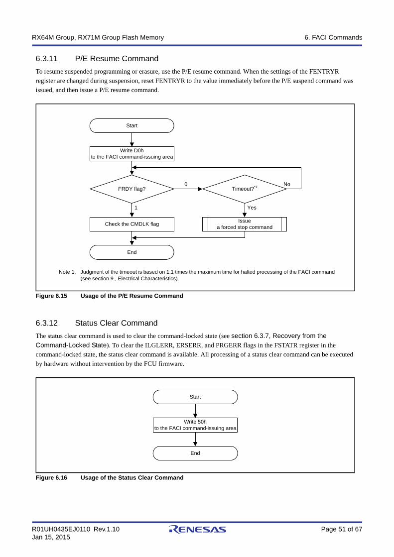
R01UH0435EJ0110 Rev.1.10 Page 51 of 67Jan 15, 2015
RX64M Group, RX71M Group Flash Memory 6. FACI Commands
6.3.11 P/E Resume Command
To resume suspended programming or erasure, use the P/E resume command. When the settings of the FENTRYR register are changed during suspension, reset FENTRYR to the value immediately before the P/E suspend command was issued, and then issue a P/E resume command.
Figure 6.15 Usage of the P/E Resume Command
6.3.12 Status Clear Command
The status clear command is used to clear the command-locked state (see section 6.3.7, Recovery from the
Command-Locked State). To clear the ILGLERR, ERSERR, and PRGERR flags in the FSTATR register in the command-locked state, the status clear command is available. All processing of a status clear command can be executed by hardware without intervention by the FCU firmware.
Figure 6.16 Usage of the Status Clear Command
Start
Issuea forced stop command
End
Check the CMDLK flag
Timeout?*1No
Yes
FRDY flag?0
1
Write D0hto the FACI command-issuing area
Note 1. Judgment of the timeout is based on 1.1 times the maximum time for halted processing of the FACI command (see section 9., Electrical Characteristics).
Start
End
Write 50hto the FACI command-issuing area
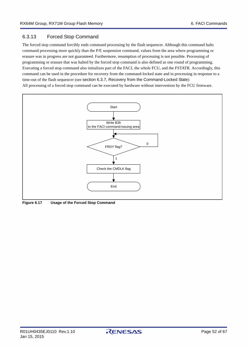
R01UH0435EJ0110 Rev.1.10 Page 52 of 67Jan 15, 2015
RX64M Group, RX71M Group Flash Memory 6. FACI Commands
6.3.13 Forced Stop Command
The forced stop command forcibly ends command processing by the flash sequencer. Although this command halts command processing more quickly than the P/E suspension command, values from the area where programming or erasure was in progress are not guaranteed. Furthermore, resumption of processing is not possible. Processing of programming or erasure that was halted by the forced stop command is also defined as one round of programming. Executing a forced stop command also initializes part of the FACI, the whole FCU, and the FSTATR. Accordingly, this command can be used in the procedure for recovery from the command-locked state and in processing in response to a time-out of the flash sequencer (see section 6.3.7, Recovery from the Command-Locked State)All processing of a forced stop command can be executed by hardware without intervention by the FCU firmware.
Figure 6.17 Usage of the Forced Stop Command
Start
End
Check the CMDLK flag
FRDY flag?0
1
Write B3hto the FACI command-issuing area
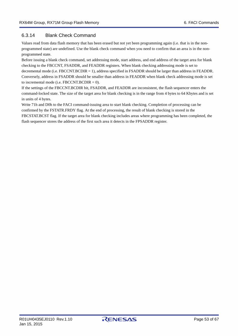
R01UH0435EJ0110 Rev.1.10 Page 53 of 67Jan 15, 2015
RX64M Group, RX71M Group Flash Memory 6. FACI Commands
6.3.14 Blank Check Command
Values read from data flash memory that has been erased but not yet been programming again (i.e. that is in the non-programmed state) are undefined. Use the blank check command when you need to confirm that an area is in the non-programmed state.Before issuing a blank check command, set addressing mode, start address, and end address of the target area for blank checking to the FBCCNT, FSADDR, and FEADDR registers. When blank checking addressing mode is set to decremental mode (i.e. FBCCNT.BCDIR = 1), address specified in FSADDR should be larger than address in FEADDR. Conversely, address in FSADDR should be smaller than address in FEADDR when blank check addressing mode is set to incremental mode (i.e. FBCCNT.BCDIR = 0).If the settings of the FBCCNT.BCDIR bit, FSADDR, and FEADDR are inconsistent, the flash sequencer enters the command-locked state. The size of the target area for blank checking is in the range from 4 bytes to 64 Kbytes and is set in units of 4 bytes.Write 71h and D0h to the FACI command-issuing area to start blank checking. Completion of processing can be confirmed by the FSTATR.FRDY flag. At the end of processing, the result of blank checking is stored in the FBCSTAT.BCST flag. If the target area for blank checking includes areas where programming has been completed, the flash sequencer stores the address of the first such area it detects in the FPSADDR register.
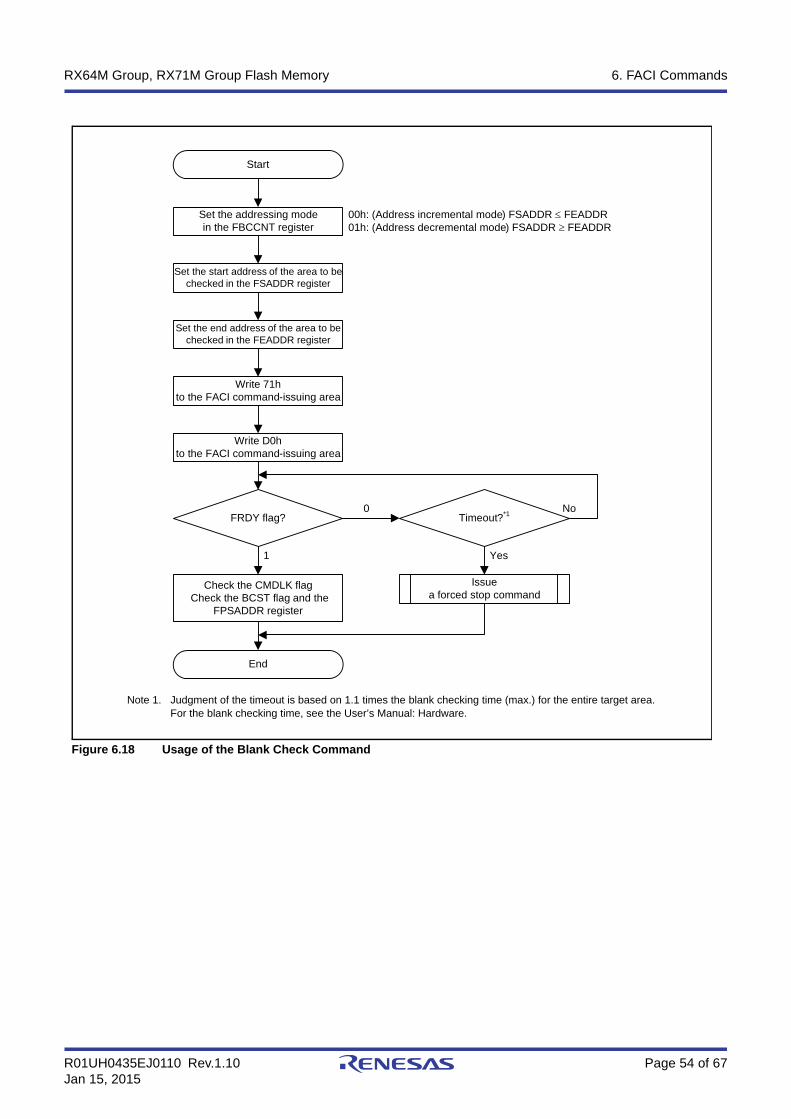
R01UH0435EJ0110 Rev.1.10 Page 54 of 67Jan 15, 2015
RX64M Group, RX71M Group Flash Memory 6. FACI Commands
Figure 6.18 Usage of the Blank Check Command
Start
Issuea forced stop command
End
Check the CMDLK flag Check the BCST flag and the
FPSADDR register
Timeout?*1No
Yes
Set the addressing modein the FBCCNT register
00h: (Address incremental mode) FSADDR FEADDR01h: (Address decremental mode) FSADDR FEADDR
Set the start address of the area to be checked in the FSADDR register
Set the end address of the area to be checked in the FEADDR register
Write 71hto the FACI command-issuing area
Write D0hto the FACI command-issuing area
FRDY flag?0
1
Note 1. Judgment of the timeout is based on 1.1 times the blank checking time (max.) for the entire target area.For the blank checking time, see the User’s Manual: Hardware.
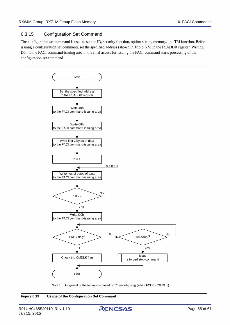
R01UH0435EJ0110 Rev.1.10 Page 55 of 67Jan 15, 2015
RX64M Group, RX71M Group Flash Memory 6. FACI Commands
6.3.15 Configuration Set Command
The configuration set command is used to set the ID, security function, option-setting memory, and TM function. Before issuing a configuration set command, set the specified address (shown in Table 6.5) in the FSADDR register. Writing D0h to the FACI command-issuing area in the final access for issuing the FACI command starts processing of the configuration set command.
Figure 6.19 Usage of the Configuration Set Command
Start
Issuea forced stop command
End
Check the CMDLK flag
n = 7?
Timeout?*1No
Yes
Set the specified addressto the FSADDR register
Write 40hto the FACI command-issuing area
Write 08hto the FACI command-issuing area
Write first 2 bytes of datato the FACI command-issuing area
n = 1
Write next 2 bytes of datato the FACI command-issuing area
Write D0hto the FACI command-issuing area
FRDY flag?
No
Yes
n = n + 1
0
1
Note 1. Judgment of the timeout is based on 70 ms elapsing (when FCLK 20 MHz).
R01UH0435EJ0110 Rev.1.10 Page 56 of 67Jan 15, 2015
RX64M Group, RX71M Group Flash Memory 6. FACI Commands
The correspondence between the possible target data for configuration setting and the address value set in the FSADDR register is shown in Table 6.5. For details on the FSADDR register, see section 4.5, FACI Command Start Address
Register (FSADDR). Data in other areas can be changed to any value each time the configuration set command is executed.
Table 6.5 Address Used by Configuration Set Command
AddressFSADDR Register Value Setting Data
0012 0040h 0000 0040h Serial programmer command control register (SPCC), TM enable flag register (TMEF)
0012 0050h 0000 0050h ID for authentication (OSIS)
0012 0060h 0000 0060h TM identification data register (TMINF), option function selection (OFS0, OFS1), endian selection (MDE)
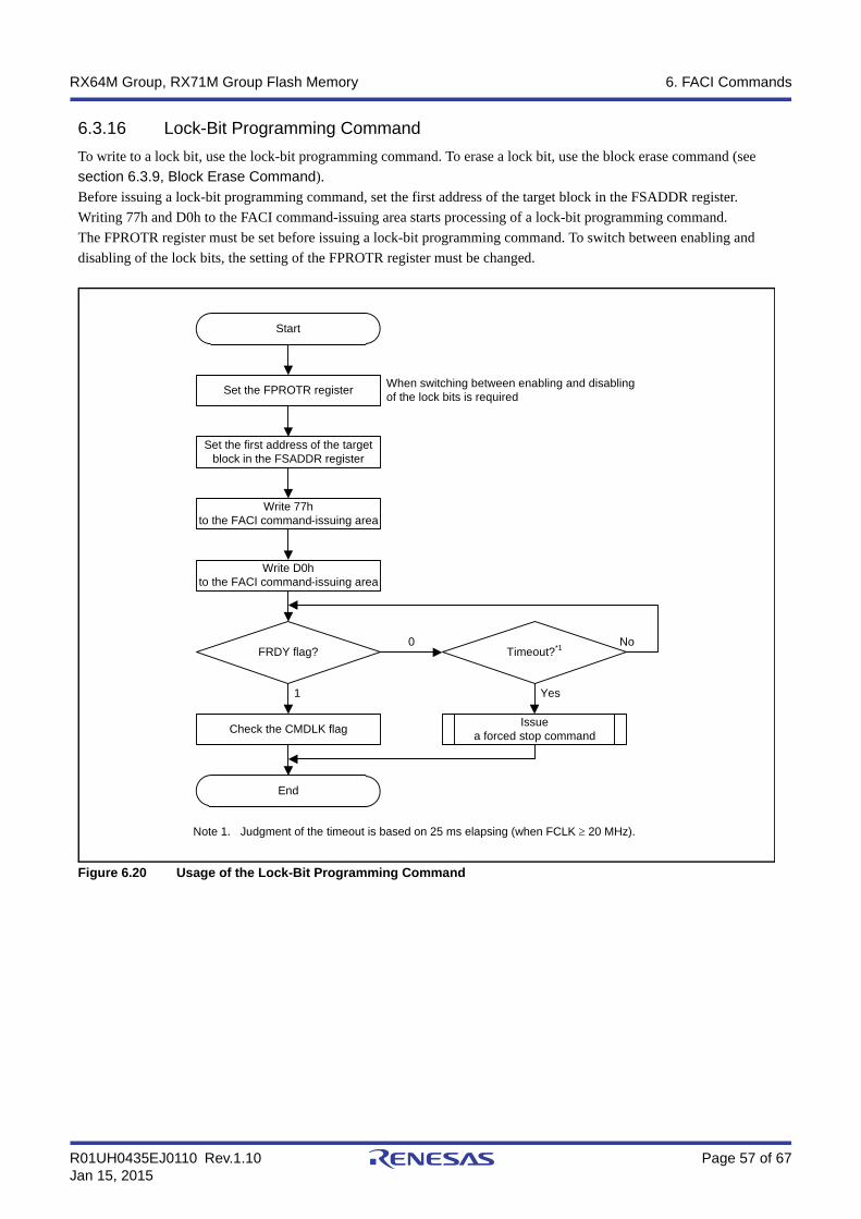
R01UH0435EJ0110 Rev.1.10 Page 57 of 67Jan 15, 2015
RX64M Group, RX71M Group Flash Memory 6. FACI Commands
6.3.16 Lock-Bit Programming Command
To write to a lock bit, use the lock-bit programming command. To erase a lock bit, use the block erase command (see section 6.3.9, Block Erase Command). Before issuing a lock-bit programming command, set the first address of the target block in the FSADDR register. Writing 77h and D0h to the FACI command-issuing area starts processing of a lock-bit programming command. The FPROTR register must be set before issuing a lock-bit programming command. To switch between enabling and disabling of the lock bits, the setting of the FPROTR register must be changed.
Figure 6.20 Usage of the Lock-Bit Programming Command
Start
Issuea forced stop command
End
Check the CMDLK flag
Timeout?*1No
Yes
Set the FPROTR registerWhen switching between enabling and disablingof the lock bits is required
Set the first address of the target block in the FSADDR register
Write 77hto the FACI command-issuing area
Write D0hto the FACI command-issuing area
FRDY flag?0
1
Note 1. Judgment of the timeout is based on 25 ms elapsing (when FCLK 20 MHz).
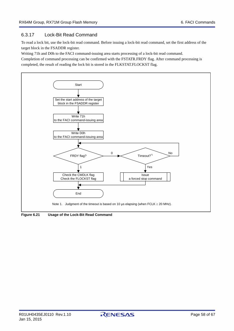
R01UH0435EJ0110 Rev.1.10 Page 58 of 67Jan 15, 2015
RX64M Group, RX71M Group Flash Memory 6. FACI Commands
6.3.17 Lock-Bit Read Command
To read a lock bit, use the lock-bit read command. Before issuing a lock-bit read command, set the first address of the target block in the FSADDR register.Writing 71h and D0h to the FACI command-issuing area starts processing of a lock-bit read command.Completion of command processing can be confirmed with the FSTATR.FRDY flag. After command processing is completed, the result of reading the lock bit is stored in the FLKSTAT.FLOCKST flag.
Figure 6.21 Usage of the Lock-Bit Read Command
Start
Issuea forced stop command
End
Check the CMDLK flagCheck the FLOCKST flag
Timeout?*1No
Yes
Set the start address of the target block in the FSADDR register
Write 71hto the FACI command-issuing area
Write D0hto the FACI command-issuing area
FRDY flag?0
1
Note 1. Judgment of the timeout is based on 10 μs elapsing (when FCLK 20 MHz).
R01UH0435EJ0110 Rev.1.10 Page 59 of 67Jan 15, 2015
RX64M Group, RX71M Group Flash Memory 7. Safety Function
7. Safety Function
7.1 Software Protection
Software protection disables programming and erasure for the code flash memory through the settings of control registers and lock bit settings in the user area. If an attempt is made to issue an FACI command against software protection, the flash sequencer enters the command-locked state.
7.1.1 Protection through FWEPROR
Unless the FWEPROR.FLWE[1:0] bits are set to 01b, programming cannot proceed in any mode.
7.1.2 Protection through FENTRYR
When the FENTRYR register is set to 0000h, the flash sequencer enters read mode. In read mode, FACI commands cannot be accepted. If an attempt is made to issue an FACI command in read mode, the flash sequencer enters the command-locked state.
7.1.3 Protection through Lock Bit
Each block in the user area includes a lock bit. When the FPROTR.FPROTCN bit is 0, blocks whose lock bit is set to 0 are prohibited from being programmed/erased. To program or erase blocks whose lock bit is set to 0, set the FPROTR.FPROTCN bit to 1. When the lock bit protection is violated and a code flash memory programming, block erase or lock-bit programming command is issued, the flash sequencer enters the command-locked state.
7.2 Error Protection
Error protection detects the issuing of illegal FACI commands, illegal access, and flash sequencer malfunction. FACI command acceptance is disabled (command-locked state) in response to the detection of these errors. The flash memory cannot be programmed or erased while the flash sequencer is in the command-locked state. For release from the command-locked state, issue a status clear or forced stop command while the CFAE and DFAE flags in the FASTAT register are 0. The status clear command can only be used while the FSTATR.FRDY flag is 1. The forced stop command can be used regardless of the value of the FSTATR.FRDY flag. While the FAEINT.CMDLKIE bit is 1, a flash access error (FIFERR) interrupt is generated if the flash sequencer enters the command-locked state (the FASTAT.CMDLK flag is set to 1).If the flash sequencer enters the command-locked state in response to a command other than the P/E suspend command during programming or erasure processing, the flash sequencer continues the processing for programming or erasure. In this state, the P/E suspend command cannot be used to suspend the processing for programming or erasure. If a command is issued in the command-locked state, the FASTAT.ILGLERR flag becomes 1 and the other bits retain the values set due to previous error detection.Table 7.1 shows error protection types and status bit values after error detection.
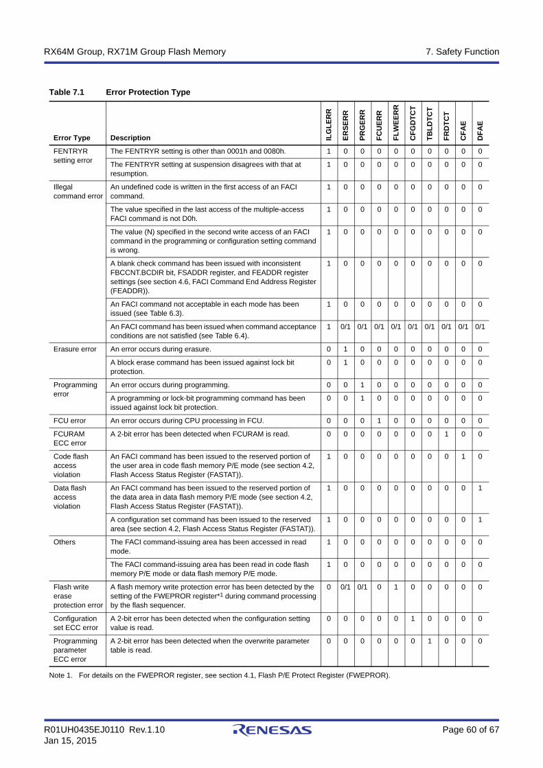
R01UH0435EJ0110 Rev.1.10 Page 60 of 67Jan 15, 2015
RX64M Group, RX71M Group Flash Memory 7. Safety Function
Note 1. For details on the FWEPROR register, see section 4.1, Flash P/E Protect Register (FWEPROR).
Table 7.1 Error Protection Type
Error Type Description ILG
LE
RR
ER
SE
RR
PR
GE
RR
FC
UE
RR
FL
WE
ER
R
CF
GD
TC
T
TB
LD
TC
T
FR
DT
CT
CF
AE
DF
AE
FENTRYR setting error
The FENTRYR setting is other than 0001h and 0080h. 1 0 0 0 0 0 0 0 0 0
The FENTRYR setting at suspension disagrees with that at resumption.
1 0 0 0 0 0 0 0 0 0
Illegal command error
An undefined code is written in the first access of an FACI command.
1 0 0 0 0 0 0 0 0 0
The value specified in the last access of the multiple-access FACI command is not D0h.
1 0 0 0 0 0 0 0 0 0
The value (N) specified in the second write access of an FACI command in the programming or configuration setting command is wrong.
1 0 0 0 0 0 0 0 0 0
A blank check command has been issued with inconsistent FBCCNT.BCDIR bit, FSADDR register, and FEADDR register settings (see section 4.6, FACI Command End Address Register (FEADDR)).
1 0 0 0 0 0 0 0 0 0
An FACI command not acceptable in each mode has been issued (see Table 6.3).
1 0 0 0 0 0 0 0 0 0
An FACI command has been issued when command acceptance conditions are not satisfied (see Table 6.4).
1 0/1 0/1 0/1 0/1 0/1 0/1 0/1 0/1 0/1
Erasure error An error occurs during erasure. 0 1 0 0 0 0 0 0 0 0
A block erase command has been issued against lock bit protection.
0 1 0 0 0 0 0 0 0 0
Programming error
An error occurs during programming. 0 0 1 0 0 0 0 0 0 0
A programming or lock-bit programming command has been issued against lock bit protection.
0 0 1 0 0 0 0 0 0 0
FCU error An error occurs during CPU processing in FCU. 0 0 0 1 0 0 0 0 0 0
FCURAMECC error
A 2-bit error has been detected when FCURAM is read. 0 0 0 0 0 0 0 1 0 0
Code flash access violation
An FACI command has been issued to the reserved portion of the user area in code flash memory P/E mode (see section 4.2, Flash Access Status Register (FASTAT)).
1 0 0 0 0 0 0 0 1 0
Data flash access violation
An FACI command has been issued to the reserved portion of the data area in data flash memory P/E mode (see section 4.2, Flash Access Status Register (FASTAT)).
1 0 0 0 0 0 0 0 0 1
A configuration set command has been issued to the reserved area (see section 4.2, Flash Access Status Register (FASTAT)).
1 0 0 0 0 0 0 0 0 1
Others The FACI command-issuing area has been accessed in read mode.
1 0 0 0 0 0 0 0 0 0
The FACI command-issuing area has been read in code flash memory P/E mode or data flash memory P/E mode.
1 0 0 0 0 0 0 0 0 0
Flash write erase protection error
A flash memory write protection error has been detected by the setting of the FWEPROR register*1 during command processing by the flash sequencer.
0 0/1 0/1 0 1 0 0 0 0 0
Configuration set ECC error
A 2-bit error has been detected when the configuration setting value is read.
0 0 0 0 0 1 0 0 0 0
Programming parameter ECC error
A 2-bit error has been detected when the overwrite parameter table is read.
0 0 0 0 0 0 1 0 0 0
R01UH0435EJ0110 Rev.1.10 Page 61 of 67Jan 15, 2015
RX64M Group, RX71M Group Flash Memory 7. Safety Function
7.3 Boot Program Protection
7.3.1 User Boot Protection
The user boot area can only be overwritten in programming mode (boot mode (for the SCI or USB interface)). Since this area is usually write-protected in normal operating mode and user boot mode, it can be used for the safe storage of programs such as a boot program.
R01UH0435EJ0110 Rev.1.10 Page 62 of 67Jan 15, 2015
RX64M Group, RX71M Group Flash Memory 8. Usage Notes
8. Usage Notes
(1) Reading areas where programming or erasure was interrupted
When programming or erasure of an area of flash memory is interrupted, the data stored in the area become undefined. To avoid undefined data that are read out becoming the source of faulty operation, take care not to fetch instructions or read data from areas where programming or erasure was interrupted.
(2) Prohibition of additional writing
Writing to a given area twice is not possible. If you want to overwrite data in an area of flash memory after writing to the area has been completed, erase the area first.
(3) Resets during programming and erasure
In the case of a reset due to the signal on the RES# pin during programming and erasure, wait for at least tRESWF (see the User's Manual: Hardware for details) once the operating voltage is within the range stipulated in the electrical characteristics after assertion of the reset signal before releasing the device from the reset state.
(4) Allocation of vectors for interrupts and other exceptions during programming and erasure
Generation of an interrupt or other exception during programming or erasure may lead to fetching of the vector from the code flash memory. If this does not satisfy the conditions for using background operation, set the address for vector fetching to an address that is not in the code flash memory.
(5) Abnormal termination of programming and erasure
Even if programming/erasure ends abnormally due to the generation of a reset by the RES# pin, the programming/erasure state of the flash memory with undefined data cannot be verified or checked. For the area where programming/erasure ends abnormally, the blank check function cannot judge whether the area is erased successfully or not. Erase the area again to prove that the corresponding area is completely erased before using. If programming and erasure of code flash memory are not completed normally, the lock bit for the target area may be enabled (locked). In such cases, erase the block to erase the lock bit while the lock bit is in the disabled state (the area is not locked).
(6) Items prohibited during programming and erasure
Do not perform the following operations during programming and erasure. Have the operating voltage from the power supply go beyond the allowed range. Change the frequency of the PCLK/FCLK.
R01UH0435EJ0110 Rev.1.10 Page 63 of 67Jan 15, 2015
RX64M Group, RX71M Group Flash Memory 9. Electrical Characteristics
9. Electrical Characteristics
9.1 AC Characteristics
Note: tFcyc: PCLKB/FCLK cycle
Conditions: VCC = AVCC0 = AVCC1 = VCC_USB = VBATT = 2.7 to 3.6 V, 2.7 ≤ VREFH0 ≤ AVCC0, VCC_USBA = AVCC_USBA = 3.0 to 3.6 V, VSS = AVSS0 = AVSS1 = VREFL0 = VSS_USB = VSS1_USBA = VSS2_USBA = PVSS_USBA = AVSS_USBA = 0 V, Ta = Topr
Item Min. Typ. Max. Unit Conditions
FCURAM data transfer time — 220 — μs FCLK = 60 MHz and the FRAMTRAN bit in the FCURAME register is 0
— 110 — μs FCLK = 60 MHz and the FRAMTRAN bit in the FCURAME register is 1
FACI command setup time — — 100 μs FCLK ≥ 20 MHz
FACI command proccessing time — — 0 tFcyc For other than programming of code flash memory
— — 90 tFcyc For programming of code flash memory
Forced stop command — — 20 μs 20MHz ≤ FCLK ≤ 60MHz
— — 32 μs FCLK = 4MHz
R01UH0435EJ0110 Rev.1.10 Page 64 of 67Jan 15, 2015
RX64M Group, RX71M Group Flash Memory REVISION HISTORY
REVISION HISTORY RX64M Group Flash Memory User’s Manual: Hardware Interface
Rev. DateDescription
Page Summary
0.90 May 30, 2014 — First edition, issued
1.00 Jul 31, 2014 6. FACI Commands
8 Table 3.1 Information on the Hardware Interface Area, changed
32 Table 6.1 List of FACI Commands, changed
55 6.3.15 Configuration Set Command, changed
56 Table 6.5 Address Used by Configuration Set Command, changed
60 Table 7.1 Error Protection Type, changed
1.10 Nov 05, 2014 — RX71M group, added
All Terms unified:RX64M User’s Manual: Hardware or RX71M User’s Manual: Hardware → User’s Manual: Hard-ware
1. Features
6 Body text changed
2. Module Configuration
7 Body text changed
4. Registers
10 4.1 Flash P/E Protect Register (FWEPROR), changed
11 4.2 Flash Access Status Register (FASTAT), changed
13 4.3 Flash Access Error Interrupt Enable Register (FAEINT)
15 4.5 FACI Command Start Address Register (FSADDR), changed
16 4.6 FACI Command End Address Register (FEADDR), changed
17 4.7 FCURAM Enable Register (FCURAME), changed
22 4.9 Flash P/E Mode Entry Register (FENTRYR), changed
23 4.10 Flash Protection Register (FPROTR), changed
24 4.11 Flash Sequencer Set-Up Initialization Register (FSUINITR), changed
27 4.14 Flash P/E Status Register (FPESTAT), changed
30 4.19 Flash Sequencer Processing Clock Notification Register (FPCKAR), changed
6. FACI Commands
32 Table 6.1 List of FACI Commands, changed
33 6.2 Relationship between the Flash Sequencer State and FACI Commands, changed
35 Figure 6.1 Overview of Command Usage in Code Flash Memory P/E Mode (for products in which BGO is possible), changed
36 Figure 6.2 Overview of Command Usage in Code Flash Memory P/E Mode (for products in which BGO is not possible), changed
37 Figure 6.3 Overview of Command Usage in Data Flash Memory P/E Mode, changed
40 Figure 6.7 Procedure for Transition to Read Mode, changed
44 Figure 6.9 Usage of the Programming Command, changed
46 6.3.10 P/E Suspend Command, changed
48 Figure 6.12 Suspension during Programming, changed
54 Figure 6.18 Usage of the Blank Check Command, changed
55, 56 6.3.15 Configuration Set Command, changedTable 6.5 Address Used by Configuration Set Command, changed
7. Safety Function
59 7.1.3 Protection through Lock Bit, changed
60 Table 7.1 Error Protection Type, changed
8. Usage Notes
62 (3) Resets during programming and erasure, changed
REVISION HISTORY
RX64M Group, RX71M Group User’s Manual: Hardware Interface
Publication Date: Rev.0.90 May 30, 2014Rev.1.10 Jan 15, 2015
Published by: Renesas Electronics Corporation
Colophon
http://www.renesas.comRefer to "http://www.renesas.com/" for the latest and detailed information.
Renesas Electronics America Inc.2801 Scott Boulevard Santa Clara, CA 95050-2549, U.S.A.Tel: +1-408-588-6000, Fax: +1-408-588-6130
Renesas Electronics Canada Limited9251 Yonge Street, Suite 8309 Richmond Hill, Ontario Canada L4C 9T3Tel: +1-905-237-2004
Renesas Electronics Europe LimitedDukes Meadow, Millboard Road, Bourne End, Buckinghamshire, SL8 5FH, U.KTel: +44-1628-585-100, Fax: +44-1628-585-900
Renesas Electronics Europe GmbHArcadiastrasse 10, 40472 Düsseldorf, GermanyTel: +49-211-6503-0, Fax: +49-211-6503-1327
Renesas Electronics (China) Co., Ltd.Room 1709, Quantum Plaza, No.27 ZhiChunLu Haidian District, Beijing 100191, P.R.ChinaTel: +86-10-8235-1155, Fax: +86-10-8235-7679
Renesas Electronics (Shanghai) Co., Ltd.Unit 301, Tower A, Central Towers, 555 Langao Road, Putuo District, Shanghai, P. R. China 200333Tel: +86-21-2226-0888, Fax: +86-21-2226-0999
Renesas Electronics Hong Kong LimitedUnit 1601-1611, 16/F., Tower 2, Grand Century Place, 193 Prince Edward Road West, Mongkok, Kowloon, Hong KongTel: +852-2265-6688, Fax: +852 2886-9022
Renesas Electronics Taiwan Co., Ltd.13F, No. 363, Fu Shing North Road, Taipei 10543, TaiwanTel: +886-2-8175-9600, Fax: +886 2-8175-9670
Renesas Electronics Singapore Pte. Ltd.80 Bendemeer Road, Unit #06-02 Hyflux Innovation Centre, Singapore 339949Tel: +65-6213-0200, Fax: +65-6213-0300
Renesas Electronics Malaysia Sdn.Bhd.Unit 1207, Block B, Menara Amcorp, Amcorp Trade Centre, No. 18, Jln Persiaran Barat, 46050 Petaling Jaya, Selangor Darul Ehsan, MalaysiaTel: +60-3-7955-9390, Fax: +60-3-7955-9510
Renesas Electronics India Pvt. Ltd.No.777C, 100 Feet Road, HALII Stage, Indiranagar, Bangalore, IndiaTel: +91-80-67208700, Fax: +91-80-67208777
Renesas Electronics Korea Co., Ltd.12F., 234 Teheran-ro, Gangnam-Gu, Seoul, 135-080, KoreaTel: +82-2-558-3737, Fax: +82-2-558-5141
SALES OFFICES
© 2015 Renesas Electronics Corporation. All rights reserved.
Colophon 4.0
RX64M Group, RX71M Group Flash Memory
R01UH0435EJ0110
Back cover