Embed Size (px)
Citation preview
3 Sequential Logic1
It’s a poor sort of memory that only works backward. —Lewis Carroll (1832–1898)
All the Boolean and arithmetic chips that we built in chapters 1 and 2 were
combinational2. Combinational chips compute functions that depend solely on
combinations of their input values. These relatively simple chips provide many
important processing functions (like the ALU), but they cannot maintain state.
Since computers must be able to not only compute values but also store and recall
values, they must be equipped with memory elements that can preserve data over
time. These memory elements are built from sequential chips.
The implementation of memory elements is an intricate art involving
synchronization, clocking, and feedback loops. Conveniently, most of this
complexity can be embedded in the operating logic of very low-level sequential
gates called flip-flops. Using these flip-flops as elementary building blocks, we will
specify and build all the memory devices employed by typical modern computers,
from binary cells to registers to memory banks and counters. This
1 This document is an adaptation of Chapter 3 of The Elements of Computing Systems, by Noam Nisan and Shimon Schocken, which the authors have graciously made available on their web site: http://nand2tetris.org. The entire text of the original chapter is included here, but additional material has been added to support the use of LogicCircuit (http://www.logiccircuit.org), a gate-level design and simulation system, instead of (or in addition to) the HDL-based design and simulation system included as part of Nand2Tetris. 2 “Combinational” is often replaced with “combinatorial” in the US.
42 Chapter 3
effort will complete the construction of the chip set needed to build an entire
computer—a challenge that we take up in the chapter 5.
Following a brief overview of clocks and flip-flops, the Background
section introduces all the memory chips that we will build on top of them. The next
two sections describe the chips Specification and Implementation, respectively. As
usual, all the chips mentioned in the chapter can be built and tested using the
hardware simulator supplied with the book, following the instructions given in the
final Project section.
3.1 Background
The act of ‘‘remembering something’’ is inherently time-dependent: You
remember now what has been committed to memory before. Thus, in order to build
chips that ‘‘remember’’ information, we must first develop some standard means
for representing the progression of time.
The Clock In most computers, the passage of time is represented by a master clock
that delivers a continuous train of alternating signals. The exact hardware
implementation is usually based on an oscillator that alternates continuously
between two phases labeled 0–1, low-high, tick-tock, etc. The elapsed time between
the beginning of a ‘‘tick’’ and the end of the subsequent ‘‘tock’’ is called cycle,
and each clock cycle is taken to model one discrete time unit. The current clock
phase (tick or tock) is represented by a binary signal. Using the hardware’s
circuitry, this signal is simultaneously broadcast to every sequential chip
throughout the computer platform.
Flip-Flops The most elementary sequential element in the computer is a device
called a flip-flop, of which there are several variants. In this book we use a variant
called a data flip-flop, or DFF, whose interface consists of a single-bit data input
and a single-bit data output. In addition, the DFF has a clock input that
continuously changes according to the master clock’s signal. Taken together, the
data and the clock inputs enable the DFF to implement the time-based behavior
43 Sequential Logic
out(t) = in(t – 1), where in and out are the gate’s input and output values and t is
the current clock cycle. In other words, the DFF simply outputs the input value
from the previous time unit.
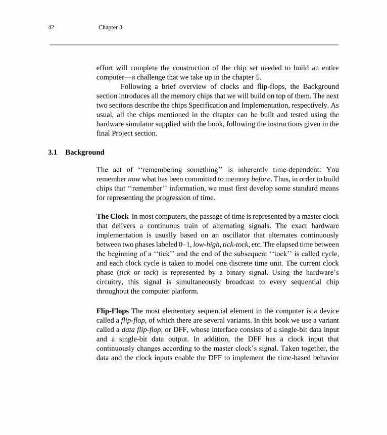
While the book as written represents the DFF as a primitive gate, the DFF
can be constructed entirely from Nand gates, as shown in Figure 3.0.
Figure 3.0 A DFF constructed from Nand gates
As we now show, the elementary behavior of DFFs can form the basis of all the
hardware devices that computers use to maintain state, from binary cells to
registers to arbitrarily large random access memory (RAM) units3.
3 Modern RAM devices do not employ DFFs to construct memory cells.
44 Chapter 3
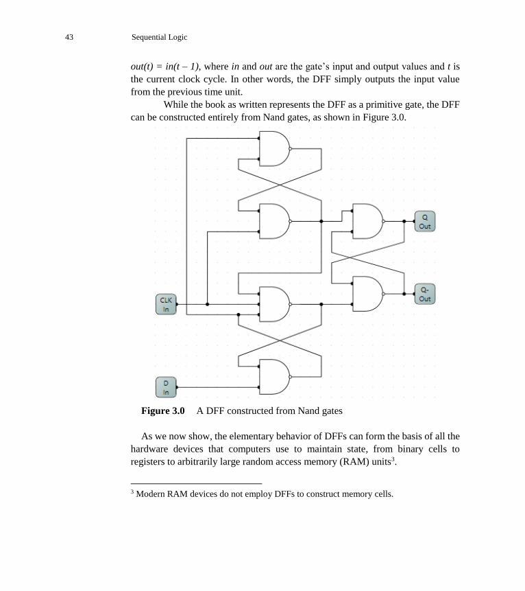
Registers A register is a storage device that can ‘‘store,’’ or ‘‘remember,’’ a value
over time, implementing the classical storage behavior out(t) = out(t - 1). A DFF,
on the other hand, can only output its previous input, e.g., out(t) = in(t - 1). This
suggests that a register can be implemented from a DFF by simply feeding the
output of the latter back into its input, creating the device shown in the middle of
Figure 3.1. Presumably, the output of this device at any time t will echo its output
at time t -1, yielding the classical function expected from a storage unit.
Figure 3.1 From a DFF to a single-bit register. The small triangle represents the
clock input. This icon is used to state that the marked chip, as well as the overall
chip that encapsulates it, is time-dependent.
Well, not so. The device shown in the middle of Figure 3.1 is invalid. First,
it is not clear how we’ll ever be able to load this device with a new data value,
since there are no means to tell the DFF when to draw its input from the in wire and
when from the out wire. More generally, the rules of chip design typically require
that internal pins must have a fan-in of 1, meaning that they can be fed from a
single source only.
The good thing about this thought experiment is that it leads us to the
correct and elegant solution shown in the right side of Figure 3.1. In particular, a
natural way to resolve our input ambiguity is to introduce a multiplexor into the
design. Further, the ‘‘select bit’’ of this multiplexor can become the ‘‘load bit’’ of
the overall register chip: If we want the register to start storing a new value, we can
put this value in the in input and set the load bit to 1; if we want the register to keep
storing its internal value until further notice, we can set the load bit to 0.
45 Sequential Logic
Once we have developed the basic mechanism for remembering a single
bit over time, we can easily construct arbitrarily wide registers. This can be
achieved by forming an array of as many single-bit registers as needed, creating a
register that holds multi-bit values (Figure 3.2). The basic design parameter of such
a register is its width—the number of bits that it holds—e.g., 16, 32, or 64. The
multi-bit contents of such registers are typically referred to as words.
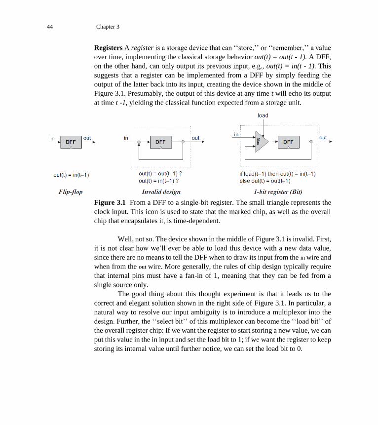
If the purpose of the “Load” input to the Bit is only to set or reset the DFF,
it is possible to design a DFF with asynchronous set and reset, as shown below in
Figure 3.1a.
Figure 3.1a A D Flip Flop with asynchronous set and reset (active low)
46 Chapter 3
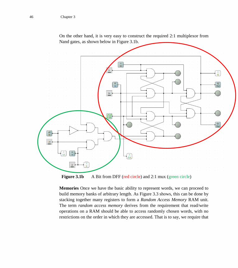
On the other hand, it is very easy to construct the required 2:1 multiplexor from
Nand gates, as shown below in Figure 3.1b.
Figure 3.1b A Bit from DFF (red circle) and 2:1 mux (green circle)
Memories Once we have the basic ability to represent words, we can proceed to
build memory banks of arbitrary length. As Figure 3.3 shows, this can be done by
stacking together many registers to form a Random Access Memory RAM unit.
The term random access memory derives from the requirement that read/write
operations on a RAM should be able to access randomly chosen words, with no
restrictions on the order in which they are accessed. That is to say, we require that
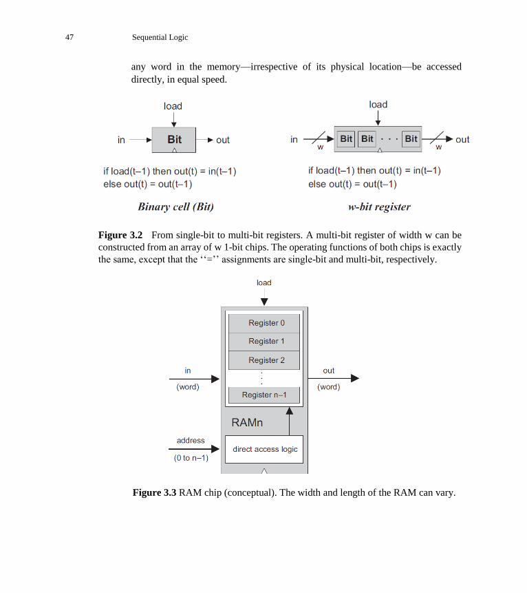
47 Sequential Logic
any word in the memory—irrespective of its physical location—be accessed
directly, in equal speed.
Figure 3.2 From single-bit to multi-bit registers. A multi-bit register of width w can be
constructed from an array of w 1-bit chips. The operating functions of both chips is exactly
the same, except that the ‘‘=’’ assignments are single-bit and multi-bit, respectively.
Figure 3.3 RAM chip (conceptual). The width and length of the RAM can vary.
This requirement can be satisfied as follows. First, we assign each word in
the n register RAM a unique address (an integer between 0 to n - 1), according to
which it will be accessed. Second, in addition to building an array of n registers,
we build a gate logic design that, given an address j, is capable of selecting the
individual register whose address is j. Note however that the notion of an
‘‘address’’ is not an explicit part of the RAM design, since the registers are not
‘‘marked’’ with addresses in any physical sense. Rather, as we will see later, the
chip is equipped with direct access logic that implements the notion of addressing
using logical means.
In sum, a classical RAM device accepts three inputs: a data input, an
address input, and a load bit. The address specifies which RAM register should be
accessed in the current time unit. In the case of a read operation (load=0), the
RAM’s output immediately emits the value of the selected register. In the case of
a write operation (load=1), the selected memory register commits to the input value
in the next time unit, at which point the RAM’s output will start emitting it.
The basic design parameters of a RAM device are its data width—the
width of each one of its words, and its size—the number of words in the RAM.
Modern computers typically employ 32- or 64-bit-wide RAMs whose sizes are up
to hundreds of millions.
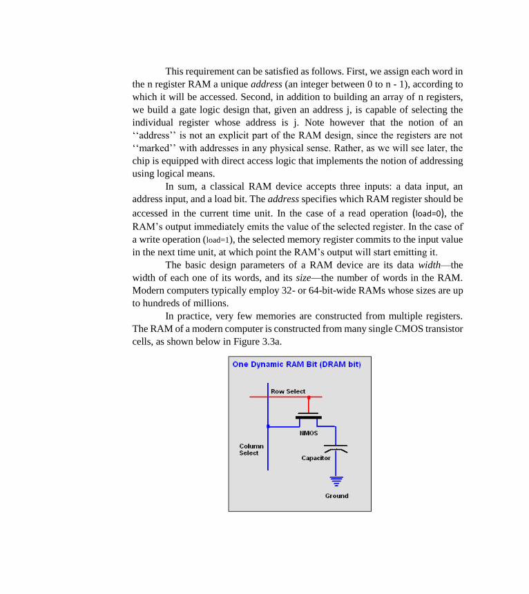
In practice, very few memories are constructed from multiple registers.
The RAM of a modern computer is constructed from many single CMOS transistor
cells, as shown below in Figure 3.3a.
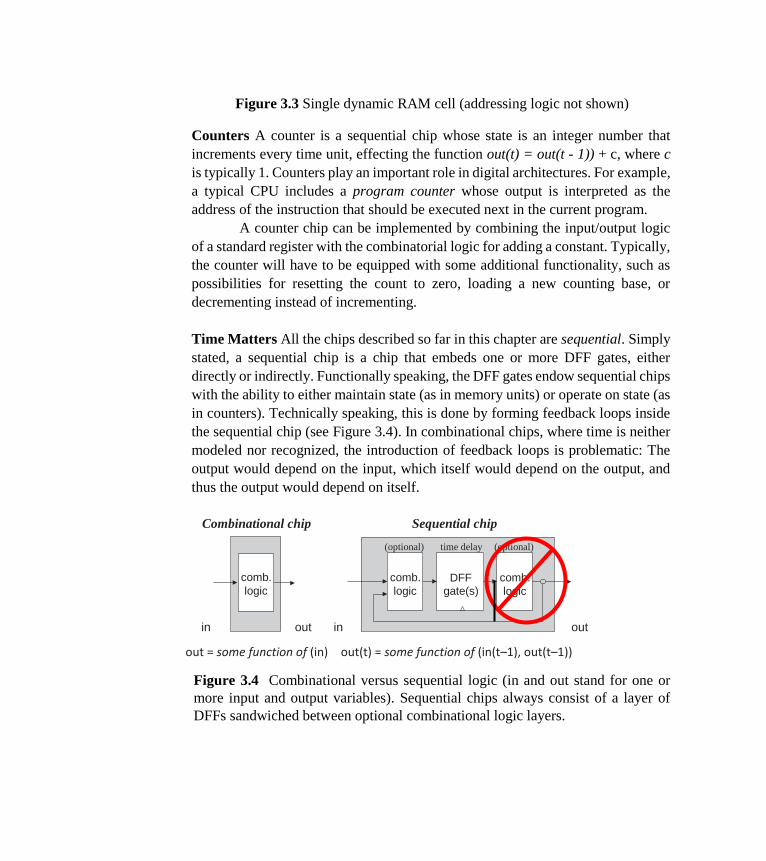
Figure 3.3 Single dynamic RAM cell (addressing logic not shown)
Counters A counter is a sequential chip whose state is an integer number that
increments every time unit, effecting the function out(t) = out(t - 1)) + c, where c
is typically 1. Counters play an important role in digital architectures. For example,
a typical CPU includes a program counter whose output is interpreted as the
address of the instruction that should be executed next in the current program.
A counter chip can be implemented by combining the input/output logic
of a standard register with the combinatorial logic for adding a constant. Typically,
the counter will have to be equipped with some additional functionality, such as
possibilities for resetting the count to zero, loading a new counting base, or
decrementing instead of incrementing.
Time Matters All the chips described so far in this chapter are sequential. Simply
stated, a sequential chip is a chip that embeds one or more DFF gates, either
directly or indirectly. Functionally speaking, the DFF gates endow sequential chips
with the ability to either maintain state (as in memory units) or operate on state (as
in counters). Technically speaking, this is done by forming feedback loops inside
the sequential chip (see Figure 3.4). In combinational chips, where time is neither
modeled nor recognized, the introduction of feedback loops is problematic: The
output would depend on the input, which itself would depend on the output, and
thus the output would depend on itself.
Combinational chip Sequential chip
in out in out
out = some function of (in) out(t) = some function of (in(t–1), out(t–1))
Figure 3.4 Combinational versus sequential logic (in and out stand for one or
more input and output variables). Sequential chips always consist of a layer of
DFFs sandwiched between optional combinational logic layers.
comb. logic
comb. logic
DFF gate(s)
comb. logic
( optional ) time delay optional ) (
As an engineering matter, the “Sequential chip” shown in Figure 3.4
represents a problematic design. In general, we only want combinatorial logic on
one side of the flip flop (usually the input side) to ensure that data and control
signals only change at well-defined times (e.g., at the rising clock edge). The
output side combinatorial logic is shown as prohibited.
On the other hand, there is no difficulty in feeding the output of a
sequential chip back into itself, since the DFFs introduce an inherent time delay:
The output at time t does not depend on itself, but rather on the output at time t-1.
This property guards against the uncontrolled ‘‘data races’’ that would occur in
combinational chips with feedback loops.
Recall that the outputs of combinational chips change when their inputs
change, irrespective of time. In contrast, the inclusion of the DFFs in the sequential
architecture ensures that their outputs change only at the point of transition from
one clock cycle to the next, and not within the cycle itself. In fact, we allow
sequential chips to be in unstable states during clock cycles, requiring only that at
the beginning of the next cycle they output correct values.
This ‘‘discretization’’ of the sequential chips’ outputs has an important
side effect: It can be used to synchronize the overall computer architecture. To
illustrate, suppose we instruct the arithmetic logic unit (ALU) to compute x + y
where x is the value of a nearby register and y is the value of a remote RAM
register. Because of various physical constraints (distance, resistance,
interference, random noise, etc.) the electric signals representing x and y will
likely arrive at the ALU at different times. However, being a combinational chip,
the ALU is insensitive to the concept of time— it continuously adds up whichever
data values happen to lodge in its inputs. Thus, it will take some time before the
ALU’s output stabilizes to the correct x + y result. Until then, the ALU will
generate garbage.
How can we overcome this difficulty? Well, since the output of the ALU
is always routed to some sort of a sequential chip (a register, a RAM location,
etc.), we don’t really care. All we have to do is ensure, when we build the
computer’s clock, that the length of the clock cycle will be slightly longer that the
time it takes a bit to travel the longest distance from one chip in the architecture to
another. This way, we are guaranteed that by the time the sequential chip updates
its state (at the beginning of the next clock cycle), the inputs that it receives from
the ALU will be valid. This, in a nutshell, is the trick that synchronizes a set of
stand-alone hardware components into a well-coordinated system, as we shall see
in chapter 5.
3.2 Specification
This section specifies a hierarchy of sequential chips:
Data-flip-flops (DFFs)
Registers (based on DFFs)
Memory banks (based on registers)
Counter chips (also based on registers)
3.2.1 Data-Flip-Flop
The most elementary sequential device that we present—the basic component
from which all memory elements will be designed—is the data flip-flop gate. A
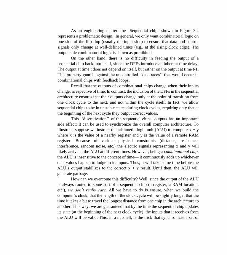
DFF gate has a single-bit input and a single-bit output, as follows:
in out
Like Nand gates, DFF gates enter our computer archtecture at a very low level.
Specifically, all the sequential chips in the computer (registers, memory, and
counters) are based on numerous DFF gates. All these DFFs are connected to the
same master clock, forming a huge distributed ‘‘chorus line.’’ At the beginning of
each clock cycle, the outputs of all the DFFs in the computer commit to their
inputs during the previous time unit. At all other times, the DFFs are ‘‘latched,’’
meaning that changes in their inputs have no immediate effect on their outputs.
This conduction operation effects any one of the millions of DFF gates that make
Chip name: DFF
Inputs: in
Outputs: out
Function: out(t)=in(t-1)
Comment: This clocked gate has a built-in implementation in HDL, and thus there is
no need to implement it. For LogicCircuit,
implement it.
DFF
up the system, about a billion times per second (depending on the computer’s
clock frequency).
Hardware implementations achieve this time dependency by simultaneously
feeding the master clock signal to all the DFF gates in the platform. Hardware
simulators emulate the same effect in software. As far as the computer architect is
concerned, the end result is the same: The inclusion of a DFF gate in the design of
any chip ensures that the overall chip, as well as all the chips up the hardware
hierarchy that depend on it, will be inherently time-dependent. These chips are
called sequential, by definition.
The physical implementation of a DFF is an intricate task, and is based on
connecting several elementary logic gates using feedback loops (one classic design
is based on Nand gates alone). In this book we have chosen to abstract away this
complexity, treating DFFs as primitive building blocks. Thus, our hardware
simulator provides a built-in DFF implementation that can be readily used by other
chips.
3.2.2 Registers
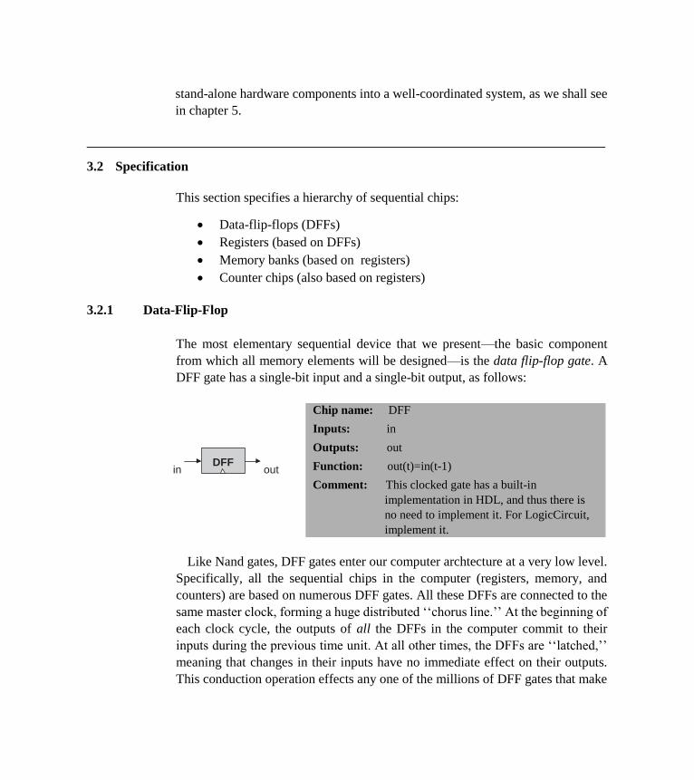
A single-bit register, which we call Bit, or binary cell, is designed to store a
single bit of information (0 or 1). The chip interface consists of an input pin that
carries a data bit, a load pin that enables the cell for writes, and an output pin that
emits the current state of the cell. The interface diagram and API of a binary cell
are as follows:
load
in out
The API of the Register chip is essentially the same, except that the input and
output pins are designed to handle multi-bit values:
Chip name: Bit
Inputs: in, load
Outputs: out
Function: If load(t-1) then out(t) = in(t-1)
else out(t) = out(t-1)
Bit
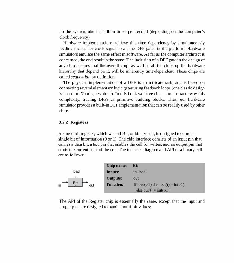
The Bit and Register chips have exactly the same read/write behavior:
Read: To read the contents of a register, we simply probe its output.
Write: To write a new data value d into a register, we put d in the in input and
assert (set to 1) the load input. In the next clock cycle, the register commits to the
new data value, and its output starts emitting d.
3.2.3 Memory
A direct-access memory unit, also called RAM, is an array of n w-bit registers,
equipped with direct access circuitry. The number of registers (n) and the width
of each register (w) are called the memory’s size and width, respectively. We will
now set out to build a hierarchy of such memory devices, all 16 bits wide, but with
varying sizes: RAM8, RAM64, RAM512, RAM4K, and RAM16K units. All these
memory chips have precisely the same API, and thus we describe them in one
parametric diagram:
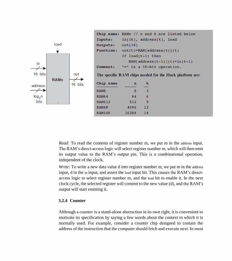
Read: To read the contents of register number m, we put m in the address input.
The RAM’s direct-access logic will select register number m, which will then emit
its output value to the RAM’s output pin. This is a combinational operation,
independent of the clock.
Write: To write a new data value d into register number m, we put m in the address
input, d in the in input, and assert the load input bit. This causes the RAM’s direct-
access logic to select register number m, and the load bit to enable it. In the next
clock cycle, the selected register will commit to the new value (d), and the RAM’s
output will start emitting it.
3.2.4 Counter
Although a counter is a stand-alone abstraction in its own right, it is convenient to
motivate its specification by saying a few words about the context in which it is
normally used. For example, consider a counter chip designed to contain the
address of the instruction that the computer should fetch and execute next. In most
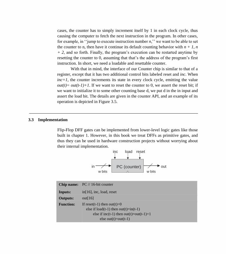
cases, the counter has to simply increment itself by 1 in each clock cycle, thus
causing the computer to fetch the next instruction in the program. In other cases,
for example, in ‘‘jump to execute instruction number n,’’ we want to be able to set
the counter to n, then have it continue its default counting behavior with n + 1, n
+ 2, and so forth. Finally, the program’s execution can be restarted anytime by
resetting the counter to 0, assuming that that’s the address of the program’s first
instruction. In short, we need a loadable and resettable counter.
With that in mind, the interface of our Counter chip is similar to that of a
register, except that it has two additional control bits labeled reset and inc. When
inc=1, the counter increments its state in every clock cycle, emitting the value
out(t)= out(t-1)+1. If we want to reset the counter to 0, we assert the reset bit; if
we want to initialize it to some other counting base d, we put d in the in input and
assert the load bit. The details are given in the counter API, and an example of its
operation is depicted in Figure 3.5.
3.3 Implementation
Flip-Flop DFF gates can be implemented from lower-level logic gates like those
built in chapter 1. However, in this book we treat DFFs as primitive gates, and
thus they can be used in hardware construction projects without worrying about
their internal implementation.
Chip name: PC // 16-bit counter
Inputs: in[16], inc, load, reset
Outputs: out[16]
Function: If reset(t-1) then out(t)=0
else if load(t-1) then out(t)=in(t-1)
else if inc(t-1) then out(t)=out(t-1)+1
else out(t)=out(t-1)
PC (counter) w bits
out in w bits
inc load reset
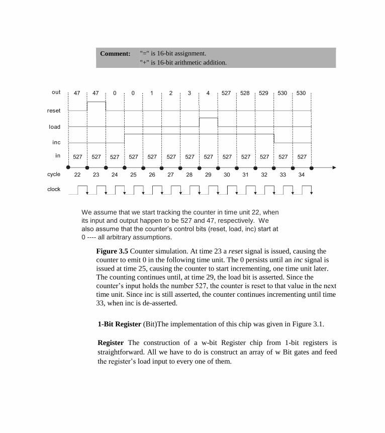
Comment: "=" is 16-bit assignment.
"+" is 16-bit arithmetic addition.
We assume that we start tracking the counter in time unit 22, when
its input and output happen to be 527 and 47, respectively. We
also assume that the counter’s control bits (reset, load, inc) start at
0 ---- all arbitrary assumptions.
Figure 3.5 Counter simulation. At time 23 a reset signal is issued, causing the
counter to emit 0 in the following time unit. The 0 persists until an inc signal is
issued at time 25, causing the counter to start incrementing, one time unit later.
The counting continues until, at time 29, the load bit is asserted. Since the
counter’s input holds the number 527, the counter is reset to that value in the next
time unit. Since inc is still asserted, the counter continues incrementing until time
33, when inc is de-asserted.
1-Bit Register (Bit)The implementation of this chip was given in Figure 3.1.
Register The construction of a w-bit Register chip from 1-bit registers is
straightforward. All we have to do is construct an array of w Bit gates and feed
the register’s load input to every one of them.
8-Register Memory (RAM8) An inspection of Figure 3.3 may be useful here. To
implement a RAM8 chip, we line up an array of eight registers. Next, we have to
build combinational logic that, given a certain address value, takes the RAM8’s in
input and loads it into the selected register. In a similar fashion, we have to build
combinational logic that, given a certain address value, selects the right register
and pipes its out value to the RAM8’s out output. Tip: This combinational logic
was already implemented in chapter 1.
n-Register Memory A memory bank of arbitrary length (a power of 2) can be
built recursively from smaller memory units, all the way down to the single
register level. This view is depicted in Figure 3.6. Focusing on the right-hand side
of the Figure, we note that a 64-register RAM can be built from an array of eight
8-register RAM chips. To select a particular register from the RAM64 memory,
we use a 6-bit address, say xxxyyy. The MSB xxx bits select one of the RAM8
chips, and the LSB yyy bits select one of the registers within the selected RAM8.
The RAM64 chip should be equipped with logic circuits that effect this
hierarchical addressing scheme. DO NOT implement a memory larger than 16
words.
Counter A w-bit counter consists of two main elements: a regular w-bit register,
and combinational logic. The combinational logic is designed to (a) compute the
counting function, and (b) put the counter in the right operating mode, as mandated
by the values of its three control bits. Tip: Most of this logic was already built in
chapter 2.
3.4 Perspective
The cornerstone of all the memory systems described in this chapter is the flip-
flop— a gate that we treated here as an atomic, or primitive, building block. The
usual approach in hardware textbooks is to construct flip-flops from elementary
combinatorial gates (e.g., Nand gates) using appropriate feedback loops. The
standard con-
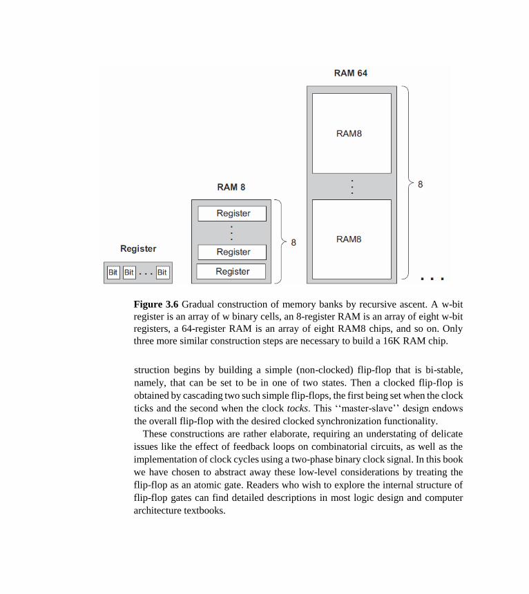
Figure 3.6 Gradual construction of memory banks by recursive ascent. A w-bit
register is an array of w binary cells, an 8-register RAM is an array of eight w-bit
registers, a 64-register RAM is an array of eight RAM8 chips, and so on. Only
three more similar construction steps are necessary to build a 16K RAM chip.
struction begins by building a simple (non-clocked) flip-flop that is bi-stable,
namely, that can be set to be in one of two states. Then a clocked flip-flop is
obtained by cascading two such simple flip-flops, the first being set when the clock
ticks and the second when the clock tocks. This ‘‘master-slave’’ design endows
the overall flip-flop with the desired clocked synchronization functionality.
These constructions are rather elaborate, requiring an understating of delicate
issues like the effect of feedback loops on combinatorial circuits, as well as the
implementation of clock cycles using a two-phase binary clock signal. In this book
we have chosen to abstract away these low-level considerations by treating the
flip-flop as an atomic gate. Readers who wish to explore the internal structure of
flip-flop gates can find detailed descriptions in most logic design and computer
architecture textbooks.
In closing, we should mention that memory devices of modern computers are
not always constructed from standard flip-flops. Instead, modern memory chips
are usually very carefully optimized, exploiting the unique physical properties of
the underlying storage technology. Many such alternative technologies are
available today to computer designers; as usual, which technology to use is a cost-
performance issue.
Aside from these low-level considerations, all the other chip constructions in
this chapter—the registers and memory chips that were built on top of the flip-flop
gates—were standard.
3.5 Project
Objective Build all the chips described in the chapter using both HDL and
LogicCircuit. For the HDL simulator, the only building blocks that you can use
are primitive DFF gates, chips that you will build on top of them, and chips
described in previous chapters. For LogicCircuit, you can use and of the gates you
built in Chapter 2.
Resources The only tool that you need for this project is the hardware simulator
supplied with the book and LogicCircuit. All the chips should be implemented in
the HDL language specified in appendix A and in LogicCircuit. As usual, for each
chip we supply a skeletal .hdl program with a missing implementation part, a .tst
script file that tells the hardware simulator how to test it, and a .cmp compare file.
Your job is to complete the missing implementation parts of the supplied .hdl
programs.
Contract When loaded into the hardware simulator, your chip design (modified
.hdl program), tested on the supplied .tst file, should produce the outputs listed in
the supplied .cmp file. If that is not the case, the simulator will let you know.
Tip The Data Flip-Flop (DFF) gate is considered primitive (in HDL) and thus
there is no need to build it when using HDL: When the simulator encounters a
DFF gate in an HDL program, it automatically invokes the built-in
tools/builtIn/DFF.hdl implementation. For Logic Circuit, implement the
DFF flip flop.
The Directory Structure of This Project When constructing RAM chips from
smaller ones, we recommend using built-in versions of the latter. Otherwise, the
simulator may run very slowly or even out of (real) memory space, since large
RAM chips contain tens of thousands of lower-level chips, and all these chips are
kept in memory (as software objects) by the simulator. For this reason, we have
placed the RAM512.hdl, RAM4K.hdl, and RAM16K.hdl programs in a separate
directory. This way, the recursive descent construction of the RAM4K and
RAM16K chips stops with the RAM512 chip, whereas the lower-level chips from
which the latter chip is made are bound to be built-in (since the simulator does not
find them in this directory).
Steps We recommend proceeding in the following order:
1. The hardware simulator needed for this project is available in the tools
directory of the book’s software suite. LogicCircuit is available on the
course web site.
2. Read appendix A, focusing on sections A.6 and A.7.
3. Go through the hardware simulator tutorial, focusing on parts IV and V.
4. Build and simulate all the chips specified in the projects/03 directory using
the HDL simulator and LogicCircuit.