Embed Size (px)
Citation preview
IC-SP-13030 R0
3-Phase BLDC Motor Driver IC
ECN30210 Product Specification Rev. 0
1. Product Description
1.1 Features
(1) Maximum Ratings: 600VDC/1.5A (condition: Tj=25℃), suitable for the system from 200VAC to
240VAC
(2) Drives a motor using high voltage PWM (Pulse Width Modulation) control and increases efficiency
(3) Variable speed control by an analog speed command signal (VSP signal)
(4) Six IGBTs, six FWDs (Free-Wheeling Diodes), drivers for IGBTs, protection circuits, etc. integrated
into a single chip, resulting in space reduction
(5) Drives a motor using a high voltage DC power supply and a low voltage DC power supply (15V)
(6) Lineup of two packages, DIP26 and SOP26 ensuring insulation distance for high voltage pins
1.2 Functions
(1) Hall elements applicable (Hall amplifiers are embedded)
(2) Power on/off sequence-free (condition: output pin current is less than 1A)
(3) Charge pump circuit (built-in high voltage diodes for charge pump)
(4) FG (Frequency Generator) signal outputs for motor rotational speed monitor (three pulses and one
pulse)
(5) All IGBT shutoff function
(6) Current limit function (detects at 0.5V)
(7) Over-current protection function (detects at 1.0V)
(8) VCC low-voltage detection function
(9) Over temperature protection function
(10) Motor lock protection function
(11) PWM circuit (enable 20kHz PWM operation)
(12) Three-phase distributor circuit
(13) VCC standby function
2/20
IC-SP-13030 R0
<ECN30210 Product Specification>
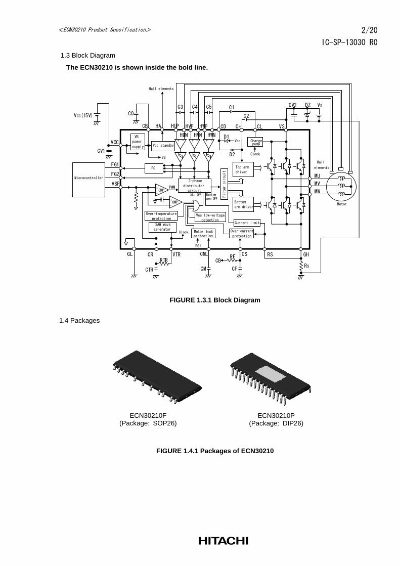
1.3 Block Diagram
The ECN30210 is shown inside the bold line.
VCC(15V)
Microcontroller
Clock
Bottomarm driver
Top armdriver
VS
MU
MV
MW
CL
GL
VS
Clock
VTR
D2
D1
C2
RTR
CTR
HUP HWPHVP
CR RS
RS
Motor
elements
+
-CMP
VSP
VCC
VB
CB
C0
C+
GH
FG1
PWM
ALL OFF Bottomarm OFF
FG2
Filter circuit
+
-CMP
C1
Vcc
HUN HVN HWN
CD
-+ -+ -+VB
FG
HA
Hall elements
C3 C4 C5
distributor
Over-temperature Vcc low-voltage
Motor lockprotection
CM
CML
FG1
CF
CSRFCB
Current limit
Over-current
Chargepump
circuit
3-phase
protection
SAW wavedetection
Hall
Vcc standby
protection
power
supply
generator
CV1
CV2 DZ
FIGURE 1.3.1 Block Diagram
1.4 Packages
FIGURE 1.4.1 Packages of ECN30210
ECN30210F (Package: SOP26)
ECN30210P (Package: DIP26)
3/20
IC-SP-13030 R0
<ECN30210 Product Specification>
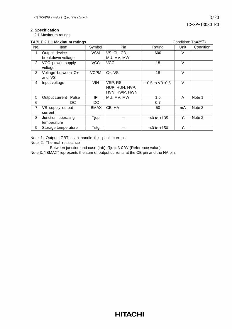
2. Specification
2.1 Maximum ratings
TABLE 2.1.1 Maximum ratings Condition: Ta=25℃
No. Item Symbol Pin Rating Unit Condition
1 Output device
breakdown voltage
VSM VS, CL, CD,
MU, MV, MW
600 V
2 VCC power supply
voltage
VCC VCC 18 V
3 Voltage between C+
and VS
VCPM C+, VS 18 V
4 Input voltage VIN VSP, RS,
HUP, HUN, HVP,
HVN, HWP, HWN
-0.5 to VB+0.5 V
5 Output current Pulse IP MU, MV, MW 1.5 A Note 1
6 DC IDC 0.7
7 VB supply output
current
IBMAX CB, HA 50 mA Note 3
8 Junction operating
temperature
Tjop - -40 to +135 ℃ Note 2
9 Storage temperature Tstg - -40 to +150 ℃
Note 1: Output IGBTs can handle this peak current.
Note 2: Thermal resistance
Between junction and case (tab): Rjc = 3℃/W (Reference value)
Note 3: “IBMAX” represents the sum of output currents at the CB pin and the HA pin.
4/20
IC-SP-13030 R0
<ECN30210 Product Specification>
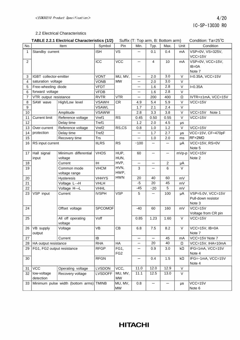
2.2 Electrical Characteristics
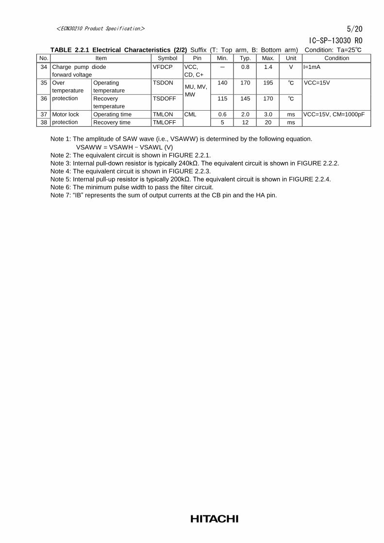
TABLE 2.2.1 Electrical Characteristics (1/2) Suffix (T: Top arm, B: Bottom arm) Condition: Ta=25℃
No. Item Symbol Pin Min. Typ. Max. Unit Condition
1 Standby current ISH VS - 0.1 0.4 mA VSP=0V, VS=325V,
VCC=15V
2 ICC VCC - 4 10 mA VSP=0V, VCC=15V,
IB=0A
Note 7
3 IGBT collector-emitter
saturation voltage
VONT MU, MV,
MW
- 2.0 3.0 V I=0.35A, VCC=15V
4 VONB - 2.0 3.0 V
5 Free-wheeling diode
forward voltage
VFDT - 1.6 2.8 V I=0.35A
6 VFDB - 1.6 2.8 V
7 VTR output resistance RVTR VTR - 200 400 Ω IVTR=±1mA, VCC=15V
8 SAW wave High/Low level VSAWH CR 4.9 5.4 5.9 V VCC=15V
9 VSAWL 1.7 2.1 2.4 V
10 Amplitude VSAWW 2.8 3.3 3.8 V VCC=15V Note 1
11 Current limit Reference voltage Vref1 RS 0.45 0.50 0.55 V VCC=15V
12 Delay time Tref1 1.2 2.0 4.5 μs
13 Over-current
protection
Reference voltage Vref2 RS,CS 0.8 1.0 1.2 V VCC=15V
14 Delay time Tref2 - 1.7 2.7 μs VCC=15V, CF=470pF
RF=2MΩ 15 Recovery time Trs - 1.0 2.0 ms
16 RS input current IILRS RS -100 - - μA VCC=15V, RS=0V
Note 5
17 Hall signal
input
Minimum differential
voltage
VHOS HUP,
HUN,
HVP,
HVN,
HWP,
HWN
60 - - mVp-p VCC=15V
Note 2
18 Current IH - - 2 μA
19 Common mode
voltage range
VHCM 3 - 6 V
20 Hysteresis VHHYS 20 40 60 mV
21 Voltage L→H VHLH -5 20 45 mV
22 Voltage H→L VHHL -45 -20 5 mV
23 VSP input Current IVSPH VSP 5 - 100 μA VSP=5.0V, VCC=15V
Pull-down resistor
Note 3
24 Offset voltage SPCOMOF -40 60 160 mV VCC=15V
Voltage from CR pin
25 All off operating
voltage
Voff 0.85 1.23 1.60 V VCC=15V
26 VB supply
output
Voltage VB CB 6.8 7.5 8.2 V VCC=15V, IB=0A
Note 7
27 Current IB - - 45 mA VCC=15V Note 7
28 HA output resistance RHA HA - 20 40 Ω VCC=15V, IHA=10mA
29 FG1, FG2 output resistance RFGP FG1,
FG2
- 0.9 3.0 kΩ IFG=1mA, VCC=15V
Note 4
30 RFGN - 0.4 1.5 kΩ IFG=-1mA, VCC=15V
Note 4
31 VCC
low-voltage
detection
Operating voltage LVSDON VCC,
MU, MV,
MW
11.0 12.0 12.9 V
32 Recovery voltage LVSDOFF 11.1 12.5 13.0 V
33 Minimum pulse width (bottom arms) TMINB MU, MV,
MW
0.8 - - μs VCC=15V
Note 6
5/20
IC-SP-13030 R0
<ECN30210 Product Specification>
TABLE 2.2.1 Electrical Characteristics (2/2) Suffix (T: Top arm, B: Bottom arm) Condition: Ta=25℃ No. Item Symbol Pin Min. Typ. Max. Unit Condition
34 Charge pump diode
forward voltage
VFDCP VCC,
CD, C+
- 0.8 1.4 V I=1mA
35 Over
temperature
protection
Operating
temperature
TSDON MU, MV,
MW
140 170 195 ℃ VCC=15V
36 Recovery
temperature
TSDOFF 115 145 170 ℃
37 Motor lock
protection
Operating time TMLON CML 0.6 2.0 3.0 ms VCC=15V, CM=1000pF
38 Recovery time TMLOFF 5 12 20 ms
Note 1: The amplitude of SAW wave (i.e., VSAWW) is determined by the following equation.
VSAWW = VSAWH - VSAWL (V)
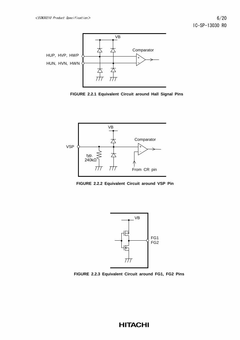
Note 2: The equivalent circuit is shown in FIGURE 2.2.1.
Note 3: Internal pull-down resistor is typically 240kΩ. The equivalent circuit is shown in FIGURE 2.2.2.
Note 4: The equivalent circuit is shown in FIGURE 2.2.3.
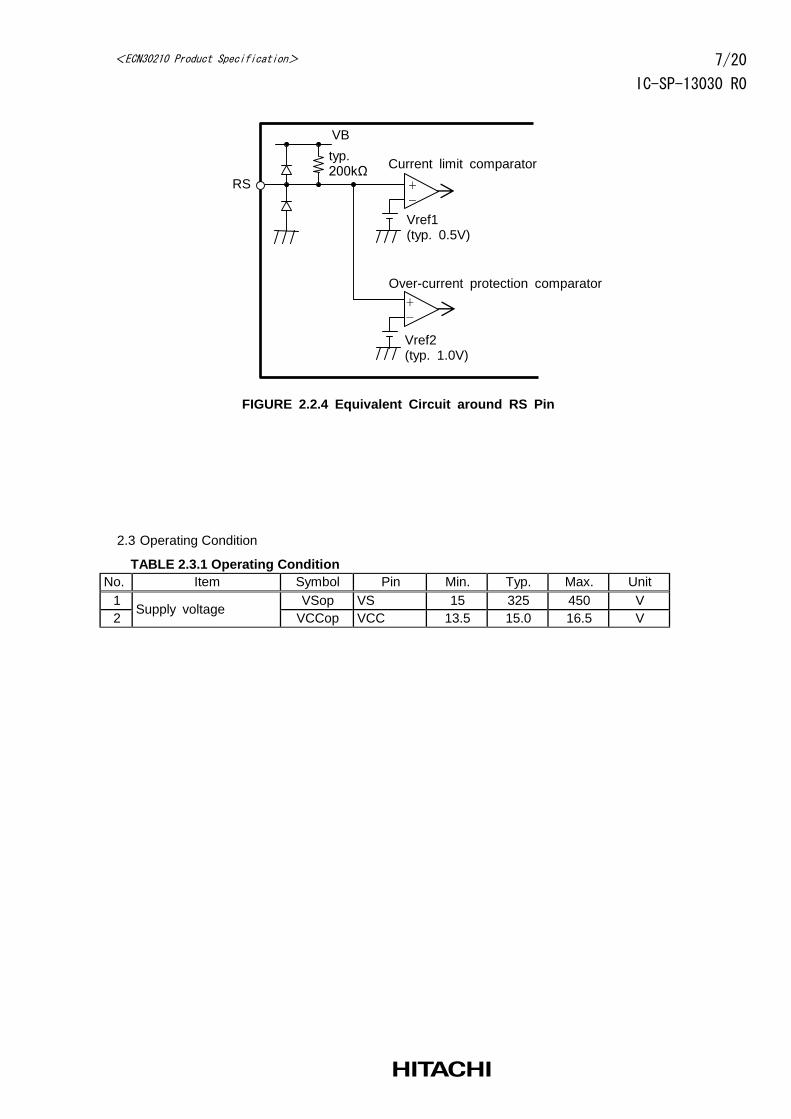
Note 5: Internal pull-up resistor is typically 200kΩ. The equivalent circuit is shown in FIGURE 2.2.4.
Note 6: The minimum pulse width to pass the filter circuit.
Note 7: “IB” represents the sum of output currents at the CB pin and the HA pin.
6/20
IC-SP-13030 R0
<ECN30210 Product Specification>
FIGURE 2.2.1 Equivalent Circuit around Hall Signal Pins
Comparator
HUP, HVP, HWP
VB
+
- HUN, HVN, HWN
FIGURE 2.2.2 Equivalent Circuit around VSP Pin
Comparator
VSP
From CR pin
typ. 240kΩ
VB
+ -
VB
FG1 FG2
FIGURE 2.2.3 Equivalent Circuit around FG1, FG2 Pins
7/20
IC-SP-13030 R0
<ECN30210 Product Specification>
2.3 Operating Condition
TABLE 2.3.1 Operating Condition
No. Item Symbol Pin Min. Typ. Max. Unit
1 Supply voltage
VSop VS 15 325 450 V
2 VCCop VCC 13.5 15.0 16.5 V
FIGURE 2.2.4 Equivalent Circuit around RS Pin
Vref1 (typ. 0.5V)
typ. 200kΩ
VB
RS
Current limit comparator
- +
Vref2 (typ. 1.0V)
- +
Over-current protection comparator
8/20
IC-SP-13030 R0
<ECN30210 Product Specification>
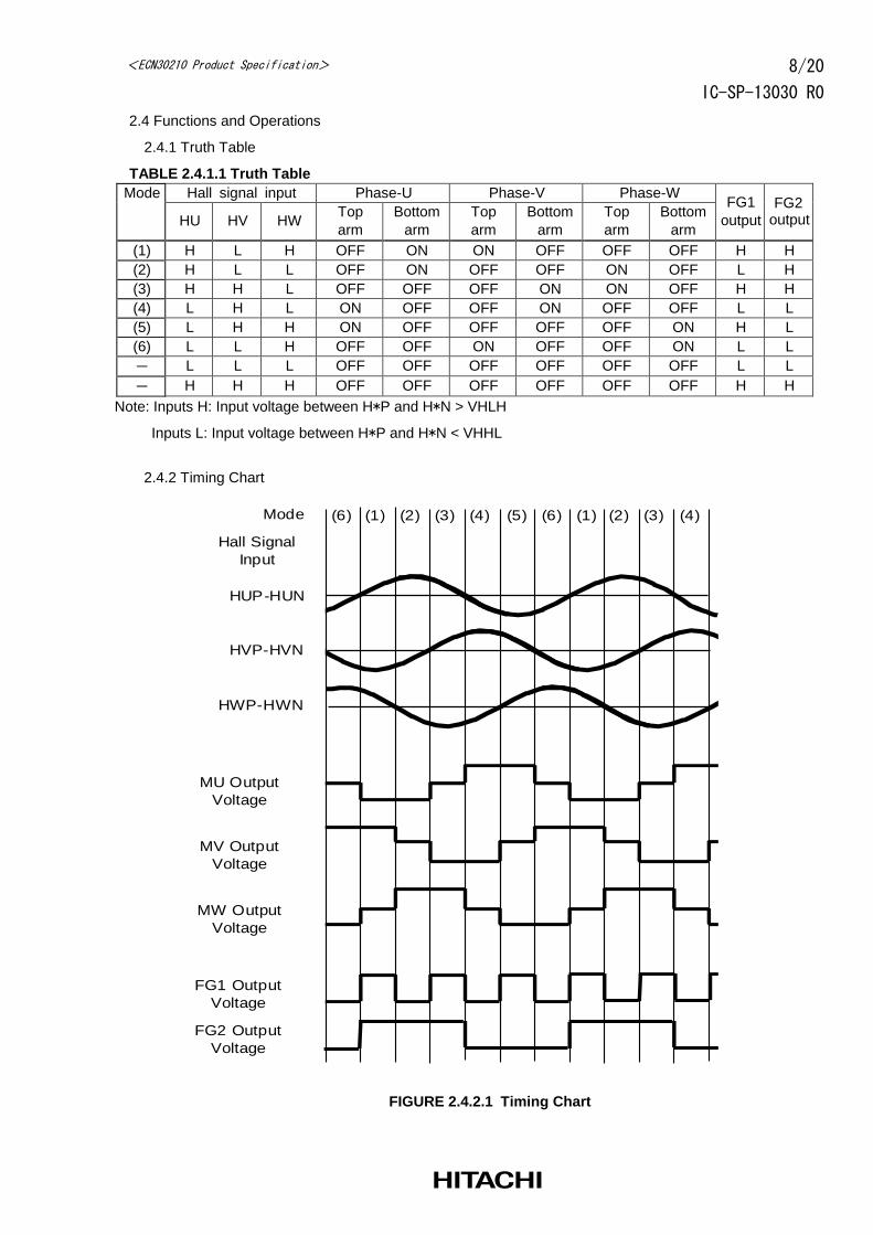
2.4 Functions and Operations
2.4.1 Truth Table
TABLE 2.4.1.1 Truth Table
Mode Hall signal input Phase-U Phase-V Phase-W FG1
output
FG2 output HU HV HW
Top
arm
Bottom
arm
Top
arm
Bottom
arm
Top
arm
Bottom
arm
(1) H L H OFF ON ON OFF OFF OFF H H
(2) H L L OFF ON OFF OFF ON OFF L H
(3) H H L OFF OFF OFF ON ON OFF H H
(4) L H L ON OFF OFF ON OFF OFF L L
(5) L H H ON OFF OFF OFF OFF ON H L
(6) L L H OFF OFF ON OFF OFF ON L L
- L L L OFF OFF OFF OFF OFF OFF L L
- H H H OFF OFF OFF OFF OFF OFF H H
Note: Inputs H: Input voltage between H*P and H*N > VHLH
Inputs L: Input voltage between H*P and H*N < VHHL
2.4.2 Timing Chart
MU Output
Voltage
MV Output
Voltage
MW Output
Voltage
FG1 Output
Voltage
Mode (1) (2) (3) (4) (5) (6) (1) (2) (3) (4) (6)
FG2 Output
Voltage
HUP-HUN
HVP-HVN
HWP-HWN
Hall Signal
Input
FIGURE 2.4.2.1 Timing Chart
9/20
IC-SP-13030 R0
<ECN30210 Product Specification>
2.4.3 PWM Operation The PWM signal is generated by comparing the input voltage at the VSP pin with an internal
SAW wave voltage (available at the CR pin). The relation between VSP input voltage and PWM
duty is shown in FIGURE 2.4.3.1. The PWM duty represents the duty of IGBT gate drive signals.
The voltages at output pins (MU,MV,MW) may be different from the figure depending on
conditions. The PWM is operated by bottom arms.
FIGURE 2.4.3.1 Relation between VSP Input Voltage and PWM Duty
2.4.4 Current Limit
This IC detects current using an external shunt resistor Rs. When the voltage at the shunt resistor Rs
exceeds the current limit reference voltage (Vref1, typ. 0.5V), all bottom arm IGBTs are turned off. This
off state is automatically reset once per internal CLOCK period (available at VTR pin).
2.4.5 Over-current Protection
When the voltage at the shunt resistor Rs exceeds the over-current protection reference voltage (Vref2,
typ. 1.0V), all IGBTs (top and bottom arms) are turned off. When the over-current protection recovery
time (Trs, typ. 1ms) passes, the IC returns to the state in which the IGBTs operate depending on input
signals.
When this function is not used, connect the CS pin to the CB pin.
2.4.6 VCC Low-Voltage Detection
When VCC voltage drops below the operating voltage of the VCC low-voltage detection (LVSDON), all
IGBTs (top and bottom arms) are turned off. When VCC voltage goes up above the recovery voltage of
the VCC low-voltage detection (LVSDOFF), the IC returns to the state in which the IGBTs operate
depending on input signals.
2.4.7 All IGBT Shutoff Function
When the input voltage at the VSP pin drops below Voff (typ. 1.23V), all IGBTs (top and bottom arms)
are shut off. The IGBT operation to the VSP input voltage is shown in TABLE 2.4.7.1.
TABLE 2.4.7.1 IGBT Operation to VSP Input Voltage
VSP Input Voltage Top Arm IGBTs Bottom Arm IGBTs
0V≦VSP<Voff All OFF All OFF Voff≦VSP<VSAWL Based on TABLE 2.4.1 All OFF
VSAWL≦VSP Based on TABLE 2.4.1 Based on TABLE 2.4.1
While motor is rotating if all IGBTs (top and bottom arms) are shut off as a result of the operation of this
function or a protection function, the VS voltage may rise because of regenerative electric power. Also in
this condition VS must not exceed the 600VDC breakdown voltage.
0
100
VSP Input Voltage (V)
PW
M d
uty
(%)
← duty=(TMINB×fPWM)×100%
← duty=(1-TMINB×fPWM)×100%
↑ VSAWL
↑ VSAWH
fPWM : PWM frequency
10/20
IC-SP-13030 R0
<ECN30210 Product Specification>
2.4.8 Motor Lock Protection
If a motor is locked, the FG1 signal is fixed at “H” or “L”. When the operating time (t1) passes in this
state, the motor lock state is detected. Then all IGBTs (top and bottom arms) are turned off. After that,
when the recovery time (t2) passes, the IC returns to the state in which the IGBTs operate depending on
input signals.
The operating time and recovery time are adjustable by the capacitance of the external capacitor CM.
Operating time: t1(s) = {TMLON(ms)/1000}×{CM(pF)/1000(pF)}
Recovery time: t2(s) = {TMLOFF(ms)/1000}×{CM(pF)/1000(pF)}
If the motor takes long time to start up because of low VS voltage or high-load, and so on, the motor
lock state may be detected during motor start-up. Set the capacitance of the external capacitor CM
considering star-up time variation.
The motor lock state is not detected under any of the following conditions (1) to (3).
(1) VSP input voltage ≦ typ. 2.2V
(2) VCC low-voltage detection operates.
(3) Over temperature protection operates.
When the motor lock protection is not used, connect the CML pin to the GL pin.
2.4.9 Over Temperature Protection
When IC temperature exceeds the operating temperature of over temperature protection (TSDON), all
IGBTs (top and bottom arms) are turned off. When IC temperature goes below the recovery
temperature of over temperature protection (TSDOFF), the IC returns to the state in which the IGBTs
operate depending on input signals.
2.4.10 VCC Standby Function
When the input voltage at the VSP pin is more than the all off operating voltage (Voff, typ.1.23V), the
current is applied from the HA pin to the Hall elements.
When the input voltage at the VSP pin is less than the all off operating voltage, the current to the Hall
elements is shut off to reduce standby power consumption from VCC power supply.
When the current to the Hall elements is shut off, the voltages at the Hall signal input pins (H*P, H*N) are
fixed at “L”. At this time, the FG1 and the FG2 output “L”. If there is need to confirm the motor rotating
state through the FG1 or the FG2 output signal while the VSP input voltage is below the all off operating
voltage, do not use this function (the HA pin). Use the CB pin as the power supply for the Hall elements.
When this function is not used, open the HA pin or connect it to the CB pin.
2.4.11 Power On/Off Sequence-Free
When the current at the output pins is below 1A, IGBT current saturation does not occur regardless of
power on/off sequence of the VCC power supply, VS power supply and VSP input voltage.
However, be aware that when the VS is powered on after the VCC and VSP power on with the motor
lock protection enabled, the motor may take long time to start up because the motor lock protection
operates.
FIGURE 2.4.10.1 Usage Example of Hall Elements and Internal Equivalent Circuit
CB
Hall elements
HA C0
All IGBT shutoff signal
11/20
IC-SP-13030 R0
<ECN30210 Product Specification>
3. Standard Applications
3.1 External Components
TABLE 3.1.1 External Components
Component Standard value Usage Remark
C0 1.0μF±10%, 25V Smooths the internal power supply (VB)
CV1 1.0μF±10%, 25V Smooths the Vcc power supply Note 1
CV2 33nF±10%, 630V Smooths the Vs power supply Note 2
DZ 440V,5W Absorbs Vs line surge voltage
C1, C2 0.22μF±10%, 25V For charge pump
C3, C4, C5 1000pF±10%, 25V Eliminates Hall signal noise Note 3
Rs 1Ω/1W±1% Sets current limit Note 4
CTR 2200pF±5%, 25V Sets PWM frequency Note 5
RTR 11kΩ±5%
CM 1.0μF±10%, 25V For motor lock protection
CF 470pF±10%, 25V Sets over-current protection delay time
RF 2MΩ±10%
Note 1: As necessary, increase the capacitance and add a zener diode in consideration of noise immunity.
Note 2: As necessary, increase the capacitance in consideration of noise immunity. Note 3: Optimize the capacitance corresponding to conditions. Note 4: The current limit set value can be calculated as follows.
I=Vref1/ Rs (A)
To determine the shunt resistor Rs, see TABLE 3.1.1 and Appendix.
Note 5: The PWM frequency is approximated by the following equation.
fPWM≒0.494 / (CTR×RTR) (Hz)
VCC(15V)
Microcontroller
Clock
Bottomarm driver
Top armdriver
VS
MU
MV
MW
CL
GL
VS
Clock
VTR
D2
D1
C2
RTR
CTR
HUP HWPHVP
CR RS
RS
Motor
elements
+
-CMP
VSP
VCC
VB
CB
C0
C+
GH
FG1
PWM
ALL OFF Bottomarm OFF
FG2
Filter circuit
+
-CMP
C1
Vcc
HUN HVN HWN
CD
-+ -+ -+VB
FG
HA
Hall elements
C3 C4 C5
distributor
Over-temperature Vcc low-voltage
Motor lockprotection
CM
CML
FG1
CF
CSRFCB
Current limit
Over-current
Chargepump
circuit
3-phase
protection
SAW wavedetection
Hall
Vcc standby
protection
power
supply
generator
CV1
CV2 DZ
FIGURE 3.1.1 Block Diagram (ECN30210 is shown inside the bold line.)
12/20
IC-SP-13030 R0
<ECN30210 Product Specification>
4. Pin Locations
DIP26 (Top view) SOP26 (Top view)
FIGURE 4.1 Pin Locations
5. Explanations of Pins
TABLE 5.1 Explanations of Pins Pin No. Symbol Explanation Remark
1 CL For the charge pump circuit Note 1
2 CD For the charge pump circuit Note 1
3 C+ For the charge pump circuit Note 1
4 VS High voltage power supply Note 1
5 MW W phase output Note 1
6 MV V phase output Note 1
7 MU U phase output Note 1
8 GH Emitters of bottom arm IGBTs and anodes of bottom arm FWDs
(Connected to a shunt resistor)
9 RS Input for current limit and over-current protection
10 FG2 Output for motor rotational speed monitor
(one pulse / 360 electrical degrees)
11 FG1 Output for motor rotational speed monitor
(three pulses / 360 electrical degrees)
12 HUN U phase Hall signal minus input
13 HUP U phase Hall signal plus input
14 HVN V phase Hall signal minus input
15 HVP V phase Hall signal plus input
16 HWN W phase Hall signal minus input
17 HWP W phase Hall signal plus input
18 CML For motor lock protection
19 VTR Connect a resistor to set the PWM frequency
20 CR Connect a resistor and a capacitor to set the PWM frequency
21 HA Output for VCC standby function
22 CS For over-current protection
23 CB VB power supply output
24 VSP Analog speed command signal input
25 VCC 15V power supply
26 GL Ground
Note1: High voltage pin. Because the voltage between CD and CL and the voltage between C+ and VS are
low voltage, the distances between the pins are the same as low voltage pins.
Note2: The voltage at exposed tap is the same as GL pin.
1 2
3
4
5
6
7
8 9
10
11
22 21 20 19 18
17 16 15 14 13 12
23 24 25 26 CL
CD
C+
VS
MW
MV
MU
GH RS FG2
FG1
CS HA CR VTR CML
HWP HWN HVP
HVN HUP
HUN
CB
VSP VCC
GL
22 21 20 19 18
17 16 15
14 13
12
23
24 25 26
CS HA CR VTR CML
HWP HWN HVP
HVN HUP
HUN
CB
VSP VCC GL 1
2
3
4
5
6
7
8 9
10 11
CL CD
C+
VS
MW
MV
MU
GH RS FG2
FG1
13/20
IC-SP-13030 R0
<ECN30210 Product Specification>
6. Inspection
Hundred percent inspection shall be conducted on electric characteristics at room temperature. For the
operating temperature and recovery temperature of the over temperature protection, equivalent inspections
are conducted at room temperature.
7. Cautions
7.1 Countermeasures against Electrical Static Discharge (ESD)
(a) IC needs to be dealt with caution to protect from damage by ESD. Material of container or
any device to carry semiconductor devices should be free from ESD, which may be caused
by vibration while transportation. To use electrically conductive container or aluminum sheet is
recommended as an effective countermeasure.
(b) What touches semiconductor devices such as work platform, machine and measuring and
test equipment should be grounded.
(c) Workers should be grounded connecting with high impedance around 100kΩ to 1MΩ while
dealing with semiconductor to avoid damaging IC by electric static discharge.
(d) Friction with other materials such as a high polymer should not be caused.
(e) Attention is necessary so that electric potential will be kept on the same level by short circuit
pins when PC board with mounted IC is carried and that vibration or friction might not occur.
(f) The humidity at assembly line to mount IC on circuit boards should be kept around 45 to 75
percents using humidifiers or such. If the humidity can not be controlled sufficiently, using
neutralization apparatus such as ionizers are effective.
7.2 Output Short-Circuit Protection
Short circuit (ex. load short, line-to-ground short) could break this IC. External protection is needed to
prevent IC breakdown.
7.3 Maximum Ratings
Regardless of changes in external conditions during use, “maximum ratings” should never be
exceeded in designing electronic circuits that employ products. In a case maximum ratings are
exceeded, products may be damaged or destroyed. In no event shall Hitachi Power Semiconductor
Device, Ltd. be liable for any failure in products or any secondary damage resulting from use at a value
exceeding the maximum ratings.
7.4 Derating Design
Continuous high-loaded (high temperature, high voltage, large current) operation should be
avoided and derating design should be applied, even within the ranges of the maximum ratings,
to ensure reliability.
7.5 Safe Design
Products may experience failures due to accident or unexpected surge voltages. Accordingly,
adopt safe design features, such as redundancy or prevention of erroneous action, to avoid extensive damage in the event of a failure.
7.6 Usage
Products are not designed, manufactured, or warranted to be suitable for use where extremely
high reliability is required (such as use in nuclear power control, aerospace and aviation, automobile,
traffic equipment, life-support-related medical equipment, fuel control equipment and various kinds of
safety equipment). Inclusion of products in such application shall be fully at the risk of customers.
Hitachi Power Semiconductor Device, Ltd. assumes no liability for applications assistance, customer
product design, or performance. In such cases it is advised customers to ensure circuit and/or product
safety by using semiconductor devices that assures high reliability or by means of user’s fail safe
precautions or other arrangement. (If a semiconductor device fails, there may be cases in which the
semiconductor device, wiring or wiring pattern will emit smoke or cause a fire or in which the
semiconductor device will burst.)
14/20
IC-SP-13030 R0
<ECN30210 Product Specification>
7.7 Soldering
(1) DIP26
The peak temperature of flow soldering* must be less than 260oC, and the dip time must be
less than 10 seconds. High stress by mounting, such as long time thermal stress by preheating, mechanical stress, etc, can lead to degradation or destruction. Make sure that your mounting method does not cause problem as a system.
* Flow soldering: Only pins enter a solder bath, while the resin or tab does not.
(2) SOP26
The recommended reflow soldering condition is shown in FIGURE 7.7.1.
60~120s
60~150s
30s Max
245℃ Max
240℃
6℃/s Max
217℃
3℃/s Max
200℃150℃
時間 (s)
パッ
ケー
ジ表
面温
度
(℃)
※)本プロファイルは目標仕様であり、 見直しとなる場合があります
Time (s)
Pac
kage
surf
ace t
em
pera
ture
(℃
)
FIGURE 7.7.1 Recommended Conditions for Infrared Reflow or Air Reflow
7.8 Others
See “Instructions for Use of Hitachi High-Voltage Monolithic ICs” for other precautions and instructions
on how to deal with these kinds of products.
250℃Max
245℃
15/20
IC-SP-13030 R0
<ECN30210 Product Specification>
8. Important Notices
(1) Hitachi Power Semiconductor Device, Ltd. warrants performance of its power semiconductor products
(hereinafter called “products”) to the specifications applicable at the time of sale in accordance with the
Product Specification. Testing and other quality control techniques are utilized to the extent Hitachi
Power Semiconductor Device, Ltd. needs to meet specifications described in the Product Specification.
Specific testing of all parameters of each device is not necessarily performed, except those mandated
by related laws and/or regulations.
(2) Should any claim be made within one month of product delivery about products’ failure to meet
performance described in the Product Specification, all the products in relevant lot(s) shall be re-
tested and re-delivered. Products delivered more than one month before of such claim shall not
be counted for such response.
(3) Hitachi Power Semiconductor Device, Ltd. assumes no obligation or any way of compensation should
any fault about customer’s goods using products be found in marketplace. Only in such a case fault of
Hitachi Power Semiconductor Device, Ltd. is evident and products concerned do not meet the Product
Specification, compensation shall be conducted if claimed within one year of product delivery up to
in the way of product replacement or payment of equivalent amount.
(4) Hitachi Power Semiconductor Device, Ltd. reserves the right to make changes in the Product
Specification and to discontinue mass production of the relevant products without notice. Customers are
advised before purchasing to confirm specification of the product of inquiry is the latest version and that
the relevant product is on mass production status in such a case purchasing is suspended for one year
or more.
(5) In no event shall Hitachi Power Semiconductor Device, Ltd. be liable for any damage that may result
from an accident or any other cause during operation of the user’s units according to this Product
Specification. Hitachi Power Semiconductor Device, Ltd. assumes no responsibility for any intellectual
property claims or any other problems that may result from applications of information, products or
circuits described in this Product Specification.
(6) No license is granted by this Product Specification under any patents or other rights of any
third party or Hitachi Power Semiconductor Device, Ltd.
(7) This Product Specification may not be reproduced or duplicated, in any form, in whole or in
part without the written permission of Hitachi Power Semiconductor Device, Ltd.
(8) The products (technologies) described in this Product Specification are not to be provided to
any party whose purpose in their application will hinder maintenance of international peace and
safety nor are they to be applied to that purpose by their direct purchasers or any third party. When
exporting these products (technologies), the necessary procedures are to be taken in accordance
with related laws and regulations.
16/20
IC-SP-13030 R0
<ECN30210 Product Specification>
◆Appendix - Supplementary Data
See derating information below when designing with the ECN30210.
1. Safe Operation Area (SOA) The current and voltage at output pins must not be outside the SOA shown in FIGURE A.
0
Output Pin Voltage (V)
1.5
0
SOA
Outp
ut P
in C
urr
ent
(A)
VCC=15V
Tj=25℃
450
2. Power On/Off Sequence and Current Derating for VCC
The current derating for VCC is shown in FIGURE B. Use the output pin current below the derating
curve. When the output pin current is less than 1A, power on/off sequence is free.
0.0
0.2
0.4
0.6
0.8
1.0
1.2
1.4
1.6
1.8
2.0
5 10 15 20
Ou
tpu
t P
in C
urr
en
t (A
)
Vcc (V)
FIGURE 2.1 Current Derating for VCC
(VCCop)
Tj=135℃
LVSDON min
VCCop min
FIGURE B: Current Derating for VCC
FIGURE A: SOA
17/20
IC-SP-13030 R0
<ECN30210 Product Specification>
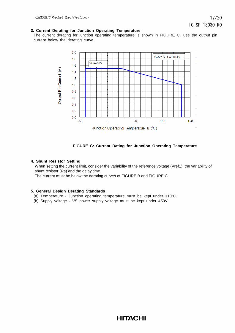
3. Current Derating for Junction Operating Temperature The current derating for junction operating temperature is shown in FIGURE C. Use the output pin
current below the derating curve.
4. Shunt Resistor Setting When setting the current limit, consider the variability of the reference voltage (Vref1), the variability of
shunt resistor (Rs) and the delay time.
The current must be below the derating curves of FIGURE B and FIGURE C.
5. General Design Derating Standards
(a) Temperature - Junction operating temperature must be kept under 110oC.
(b) Supply voltage - VS power supply voltage must be kept under 450V.
FIGURE C: Current Dating for Junction Operating Temperature
18/20
IC-SP-13030 R0
<ECN30210 Product Specification>
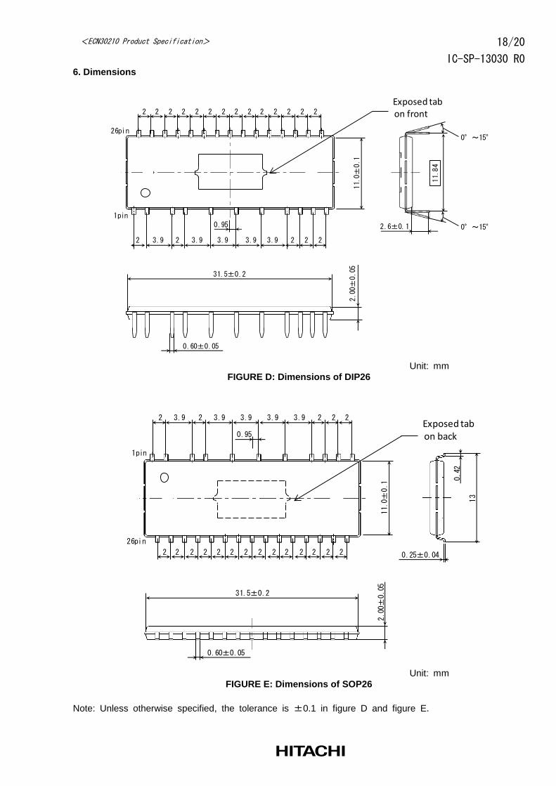
6. Dimensions
11.84
0°~15°
0°~15°2.6±0.1
31.5±0.2
2.00±
0.05
0.60±0.05
2
23.9
0.95
11.0±
0.1
2222222222222
223.93.93.93.9 22
Exposed tabon front
1pin
26pin
Unit: mm
FIGURE D: Dimensions of DIP26
0.25±0.04
13
0.42
2
23.9
0.95
11.0±
0.1
223.93.93.923.92
2222222222222
Exposed tabon back
1pin
26pin
31.5±0.2
0.60±0.05
2.00±
0.05
Unit: mm
FIGURE E: Dimensions of SOP26
Note: Unless otherwise specified, the tolerance is ±0.1 in figure D and figure E.
19/20
IC-SP-13030 R0
<ECN30210 Product Specification>
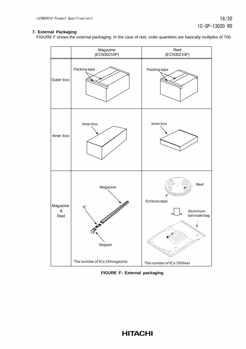
7. External Packaging FIGURE F shows the external packaging. In the case of reel, order quantities are basically multiples of 700.
Packing tape
Outer box
Inner box
Magazine
&
Reel
H
WL
内装ラベル
288273
30
リール
内装ラベル
湿度インジケータ
乾燥剤
エンボステープ
防湿袋
内装ラベル
内装箱
外装箱
外装箱
Aluminumlaminate bag
The number of ICs:700/reel
H
WL
内装ラベル
288273
30
リール
内装ラベル
湿度インジケータ
乾燥剤
エンボステープ
防湿袋
内装ラベル
内装箱
外装箱
外装箱
Emboss tape
Reel
Inner box
Packing tape
Magazine(ECN30210P)
Reel(ECN30210F)
Magazine
Stopper
IC
The number of ICs:15/magazine
Inner box
FIGURE F: External packaging
20/20
IC-SP-13030 R0
<ECN30210 Product Specification>
8. Storage conditions The following conditions are applied to ECN30210F (SOP26).
(1) Before opening the moisture prevention bag (aluminum laminate bag)
Temperature: 5 to 35℃ Humidity: less than 85%RH
Period: less than 2 years
(2) After opening the moisture prevention bag (aluminum laminate bag)
Temperature: 5 to 30℃ Humidity: less than 70%RH
Period: less than 1 week (from opening the bag to reflow soldering)
(3) Temporal strage after opening the moisture prevention bag
When ICs are stored temporarily after opening the bag they should be returned into the bags with
desiccant within 10 minutes. Then, opening side of bags should be fold into two, and close with
adhesive tape. And they should be kept in the following conditions.
Temperature: 5 to 35℃ Humidity: less than 85%RH
Period: less than 1 month