Embed Size (px)
Citation preview
Case 8:12-cv-00759-AG-MLG Document 1 Filed 05/10/12 Page 1 of 62 Page ID #:17
1 Crystal G. Foley (SBN 224627) SIMMONS BROWDER GIANARIS
2 ANGELJDES & BARNERD LLC
3 100 N. Sepulveda Blvd., Suite 1350 El Segundo, California 90245
4 Telephone: 310-322-3555
5 Facsimile: 310-322-3655 [email protected]
6
7 Attorneys for Plaintiff Labyrinth Optical Technologies LLC
8 [Additional Counsel.Listed on Signature Page] f'.' I ~'"'u1.) •'''"'•·~.~ :.· t) fl . \ 9 'A ·'~ t::. ,. ,i '"il\3 (H :~)
10 UNITED STATES DISTRICT COURT CENTRAL DISTRICT OF CALIFORNIA
11
12 LABYRINTH OPTICAL TECHNOLOGIES LLC
13 Plaintiff,
14 vs.
15 ALCATEL-LUCENT USA, INC.,
16 Defendants.
CASE NUMBER:
To be Supplied by the Clerk of The Unitea States District Court
COMPLAINT FOR PATENT INFRINGEMENTi· DEMAND FOR JURY TRIA
DATE: May 10, 2012 17
18
19 Plaintiff Labyrinth Optical Technologies LLC ("Labyrinth") files this action
20 for infringement of United States Patents No. 8,103;173 ("the '173 patent") and
21 7,599,627 ("the '627 patent") against Defendant Alcatel-Lucent USA, Inc.
22 ("Alcatel"), seeking damages and injuncti'\e relief. Labyrinth alleges as follows:
23 JURISDICTION AND VENUE
24 1. This is an action for patent infringement arising under the Patent Laws
25 of the United States, 35 U.S.C. § 1 et seq., alleging infringement of United States
26 Patent Nos. 8,103,173 ("the 'I 73 patent") and 7,599,627 ("the '627 patent").
27 Copies of the patents are attached hereto as Exhibits A-B respectively, and are
28 incorporated herein by reference in their entirety. COMPLAINT FOR PATENT INFRINGEMENT

Case 8:12-cv-00759-AG-MLG Document 1 Filed 05/10/12 Page 2 of 62 Page ID #:18
1
2 2. This Court has exclusive subject matter jurisdiction over this action
3 under 28 U.S.C. §§ 1331 and 1338(a).
4 3. This Court has personal jurisdiction over Alcatel because Alcatel has
5 conducted business in this district and has infringed, contributed to the
6 infringement, and/or actively induced others to infringe Labyrinth's patents in this
7 district as alleged in this Complaint (at a minimum by using, offering for sale
8 and/or selling products which fall within the scope of the claims of the '173 and
9 '627 patents).
10 4. Moreover, upon information and belief, Alcatel continues to conduct
11 business in this district and infringe, contribute to the infringement of, and/or
12 actively induce others to infringe the '173 and '627 patents in this district.
13 5. Venue is proper in this Court pursuant to 28 U.S.C. §§1391(b),
14 1391(c) and/or 1400(b); in that a substantial part of the events giving rise to
15 Labyrinth's claims occurred in the Central District of California and Alcatel is
16 subject to personal jurisdiction in the Central District of California (and thus for
17 purposes of venue Defendant resides in the Central District of California).
18 THEPARTIES
19 6. Plaintiff Labyrinth is !;I limited liability company organized and
20 existing under the laws of California, and hav:ing a principal place of business at . ' ·1,
21 500 Newport Center Drive, 7'h Floor, Newport Beach, California 92660.
22 7. Upon information and belief and after a reasonable opportunity for
23 further discovery, Alcatel is a corporation organized and existing under the laws of
24 the state of Delaware, having a principal place of business at 800 North Point
25 Parkway, Alpharetta, GA 30005. Alcatel's registered agent for service of process
26 in the State of California is The Prentice-Hall Corporation System, fuc., 2710
27 Gateway Oaks Dr., STE 100, Sacramento, CA 95833.
28 COMPLAINT FOR PATENT INFRINGEMENT
Case 8:12-cv-00759-AG-MLG Document 1 Filed 05/10/12 Page 3 of 62 Page ID #:19
I THE PATENTS IN SUIT
2 8. In optical data cornmimications, s~stems were upgraded from a 10
3 Gb/s data transmission rates to a 40 Gb/s transmission rates. Data transmission '
4 rates at the much faster 40 Gb/s (or higher) presented extensive design challenges
5 because the effects of polarization mode dispersion (P:MD), chromatic dispersion
6 and fiber non-linear effects such as cross-phase modulation become more
7 dominant at the higher transmission rates.
8 9. The inventors of the patents-at-issue were driven to find a cost-
9 effective method and system that compensates for P:MD, optimizes signal to noise
10 ratio performance and minimizes phase noise and nonlinearities (chromatic
11 dispersion) associated with transmission over fiber at high data transmission rates.
12 10. The '173 patent entitled "Method and System For A Polarization
13 Mode Dispersion Tolerant Optical Homodyne Detection System With Optimized
14 Transmission Modulation" was duly and legally issued on January 24, 2012.
15 11. The assignee of the '173 patent is Labyrinth. ' ·-;J'.
16 12. The '173 patent is valid and enforceable and has been at all times
17 relevant to the instant action.
18 13. The '173 patent claims a system and method for coherent optical
19 detection for an optimized transmission modulation.
20 14. For example, claim 1 of the '173 patent provides:
21 (1) A method of compensating a quadrature modulated optical data
22 signal for effects of chromatic dispersion occurring during transmission over
23 optical fiber, the method comprising the steps of:
24 (a) separating in-phase and quadrature components of the
25 optical data signal;
26
27
28
\
COMPLAINT FOR PATENT INFRINGEMENT
Case 8:12-cv-00759-AG-MLG Document 1 Filed 05/10/12 Page 4 of 62 Page ID #:20
I
2
3
4
5
6
7
8
9
10
II
12
13
14
(b) optoelectrically converting the in-phase and quadrature
components of the optical data signal into in-phase and quadrature
data signals;
(c) applying a corrective function to the in-phase and
quadrature data signals, the corrective function modifYing the in
phase and quadrature data signals in a manner that precisely
counteracts effects of chromatic dispersion on the in-phase and
quadrature components of the optical data signal.
'173 patent, Col. 12, Ins. 42-56.
15. The '627 patent entitled "Method and System For A Polarization
Mode Dispersion Tolerant Optical Homodyne Detection System With Optimized
Transmission Modulation" was duly and legally issued on October 6, 2009.
16. The assignee of the '627 patent is Labyrinth Optical Technologies
LLC.
15 17. The '627 patent is valid and enforceable and has been at all times
16 relevant to the instant action.
17 18. The '627 patent claims a system and method for coherent optical '
18 detection for an optimized transmission modulation. ' . !)
19 19. · For example, claim 22 of the '627 patent provides:
20 (22) A method of reducing the transmitted power of a quadrature
21 modulated optical data signal, comprising the steps:
.22 (a) providing a quadrature modulated optical data signal by a
23 transmitter;
24 (b) during all transitional states of the quadrature modulated
25 optical data signal in which data symbols can change in value,
26 reducing, by the transmitter, the power to zero such that transmitted
27 power decreases to zero at approximately a mid point of each of the
28 4 COMPLAINT FOR PATENT INFRINGEMENT

Case 8:12-cv-00759-AG-MLG Document 1 Filed 05/10/12 Page 5 of 62 Page ID #:21
1
2
3
4
5
6
7
transitional states, where data signals are in effect spread out by
approximately fifty percent in the fi·equency domain equivalent to a
multiplication by a sine wave at half the data rate, and results in each
symbol returning to zero at approximately a mid-point of the
transitional states.
'627 patent, Col. 16, Ins. 30-44.
THE INFRINGING PRODUCT
8 20. Defendant Alcatel, within the United States, manufactures, uses,
9 offers for sale, or sells at least Alcatel-Lucent's 1830 Photonic Service Switch,
10 Metro/regional/long-haul WDM Platform that falls within the claims of the '173
11 patent.
12 21. For purposes of an example only, Alcatel's 1830 Photonic Service
13 Switch, Metro/regional/long-haul WDM Platform falls within the scope of at least
14 claim 1 of the '173 patent as it meets each limitation recited therein. Alcatel's
15 1830 Photonic Service S:witch, Metro/regional/long-haul WDM Platform separates
16 the in-phase and the quadrature components of the optical data signal upon
17 reception, opto-electrically converts the in-phase and quadrature components of the
18 optical . data signal into in-phase and quadrature data signals, and it applies a
19 corrective function to the in-phase and quadrature data signals, which modifies the
20 in-phase and quadrature data signals that precisely counteracts effects of chromatic
21 dispersion on the optical data signal.
22 22. On belief and information only, Alcatel's 1830 Photonic Service
23 Switch, Metro/regional/long-haul WDM Platform. falls within the scope of at least
24 claim 22 of the '627 patent as it meets each limitation recited therein. Alcatel' s has
25 performed published experimental results where it uses a Carrier Suppression,
26 Return to Zero, Quadrature modulate,(:! optical data signal, which during all
27 transitional states of the quadrature modulated optical data signals, the transmitter
28 5 COMPLAINT FOR PATENT INFRINGEMENT
Case 8:12-cv-00759-AG-MLG Document 1 Filed 05/10/12 Page 6 of 62 Page ID #:22
1
2
3
4
5
6
7
8
9
10
11
12
13
reduces the power to zero such that transmitted power decreases to zero at
approximately a mid-point of each of the transitional states. Exhibit C, Chongjin
Xie et a!., Transmission of Mixed 224-Gb/s and 112-Gb/s PDM-QPSK at 50-GHz
Channel Spacing Over 1200-km Dispersion-Managed LEAF® Spans and Three
ROADMs, Joumal of Lightwave Technology, Vol. 30, No. 4, Pg. 547, February
15, 2012. On belief, Alcatel's 1830 Photonic Service Switch, Metro/regional/long
haul WDM Platform may have the limit~tions of claim 22 also.
23. Defendant Alcatel does not have a license or other authorization to
practice the claims set forth in the '627 patent.
COUNT I
Alcatel's Patent Infringement Under 35 U.S.C. §271 of the '173 Patent
24. Labyrinth incorporates by reference the allegations of paragraphs 1-
23.
14 25. Alcatel has directly or indirectly infringed the '173 patent at a
15 minimum by making, using, selling and offering for sale a product that falls within
16 the scope of the '173 patent, including, but not limited to, the Alcatel's 1830
17 Photonic Service Switch, Metro/regional/long-haul WDM Platform.
18 26. Alcatel has caused and will continue to cause Labyrinth substantial
19 damage and irreparable injury by virtue9f its continuing infringement.
20 27. Labyrinth is entitled to recover from Alcatel the damages sustained by
21 Labyrinth as a result of Alcatel's wrongful acts in an amount subject to proof at
22 trial and an injunction preventing Alcatel from continuing its wrongful acts.
23 28. Upon information and belief and after an opportunity for further
24 discovery, Alcatel's infringement of the '173 ·patent is willful and deliberate.
25 . COUNTII
26 Alcatel's Patent Infringement Under 35 U.S.C. §271 of the '627 Patent
27
28 6 COMPLAINT FOR PATENT INFRINGEMENT

Case 8:12-cv-00759-AG-MLG Document 1 Filed 05/10/12 Page 7 of 62 Page ID #:23
1 29. Labyrinth incorporates by'reference the allegations of paragraphs 1-
2 28.
3 30. Alcatel has directly or indirectly infringed the '627 patent at a
4 minimum by making, using, selling and offering for sale a product that falls within
5 the scope of the '627 patent, including, but not limited to, the Alcatel's 1830
6 Photonic Service Switch, Metro/regional/long-haul WDM Platform and publishing
7 the results of their research. Ex. C.
8 31. Alcate1 has caused and will continue to cause Labyrinth substantial
9 damage and irreparable injury by virtue of its continuing infringement.
10 32. Labyrinth is entitled to recover from Alcatel the damages sustained by
11 Labyrinth as a result of Alcatel's wrongful acts in an amount subject to proof at
12 trial and an injunction preventing Alcatel from continuing its wrongful acts.
I3 33. Upon information and belief and after an opportunity for further
14 discovery, Alcatel's infringement of the '627 patent is willful and deliberate.
15 WHEREFORE, Labyrinth respectfully requests that the Court enter a
16 judgment as follows:
17 A. That Alcatel has infringed the '173 and '627 patents under 35 U.S.C.
18 §271;
19 B. Permanently enjoining and restraining Alcatel, their officers,
20 directors, agents, servants, employees, licensees, successors, assigns, those in
21 concert and participation with them, and all persons acting on their behalf or within
22 their control under 35 U.S.C. §283 from further acts that infringe the '173 and '627
23 patents, including but not limited to, making, using, selling, offering to sell,
24 importing, exporting, advertising, or otherwise using, contributing to the use of, or
25 inducing the use of all infringing produc~s produced by Alcatel;
26 C. Requiring Alcatel to:
27
28 7 COMPLAJNT FOR PATENT lNFRlNGEMENT

Case 8:12-cv-00759-AG-MLG Document 1 Filed 05/10/12 Page 8 of 62 Page ID #:24
I 1. Send a copy of any decision in this case in favor of Labyrinth to
2 each person or entity to whom Alcatel has sold or otherwise distributed any
3 products found to infringe the '173 and '627 patents, or induced to infringe
4 the '173 and '627 patents, and informing such persons or entities of the
5 judgment and that the sale or solicited commercial transaction was wrongful;
6 . 2. Recall and collect from all persons and entities that have
7 purchased wholesale or are a distributor of any and all products found to
8 infringe the '173 and '627 patents that were made, offered for sale, sold, or
9 otherwise distributed by Alcatel, or anyone acting on its behalf;
10 3. Destroy or deliver to Labyrinth all infringing products produced
II by Alcatel; and
12 4.. File with the Court and serve upon Labyrinth, within thirty (30)
13 days after entry of final judgment in this case, a report in writing and
14 subscribed under oath setting forth in detail the form and manner in which
15 Alcatel has complied with the Court's orders as prayed for ..
16 D. Awarding Labyrinth patentinfringement damages and pre-judgment ' .·
17 interest pursuant to 35 U.S.C. §284 including, b~t not limited to, lost profits and/or
18 a reasonable royalty;
19 E. Awarding treble damages for willful infringement pursuant to 35
20 u.s.c. §284;
21 F. Declaring the case exceptional and awarding Labyrinth reasonable
22 costs and attorneys fees pursuant to 35 U.S.C. §285;
23 G. Granting Labyrinth such other and further relief as justice and equity
24 may require.
25 ///
26 ///
27 ///
28 8 COMPLAINT FOR PATENT INFRINGEMENT
Case 8:12-cv-00759-AG-MLG Document 1 Filed 05/10/12 Page 9 of 62 Page ID #:25
1
2
3
4
5
6
7
8
9
10
11
12
13
14
15
16
17
18
19
20
21
22
23
24 .
25
26
27
28
JURY DEMAND
Labyrinth requests a jury trial.
Dated: May 10,2012
Respectfully submitted, Labyrinth Optical Technologies LLC
By its attorneys, SIMMONS BROWDER GIANARIS ANGELIDES & BARNERD LLC
By: Crystal~ 100 N. Sepulveda Blvd., Suite 1350 El Segundo, California 90245 Telephone: 310-322-3555 Facsimile: 310-322-3655 Email: [email protected]
Paul A. Lesko -pro hac vice (pending) J o Anna Pollock- pro hac vice (pending) Stephen C. Smith -pro hac vice (pending) One Court Street
·Alton, IL 62002 Tel: 618-259-2222 Fax: 618-259-2251 Email: [email protected]
[email protected] [email protected]
9 COMPLAINT FOR PATENT INFRINGEMENT

Case 8:12-cv-00759-AG-MLG Document 1 Filed 05/10/12 Page 10 of 62 Page ID #:26
Exhibit A
Case 8:12-cv-00759-AG-MLG Document 1 Filed 05/10/12 Page 11 of 62 Page ID #:27
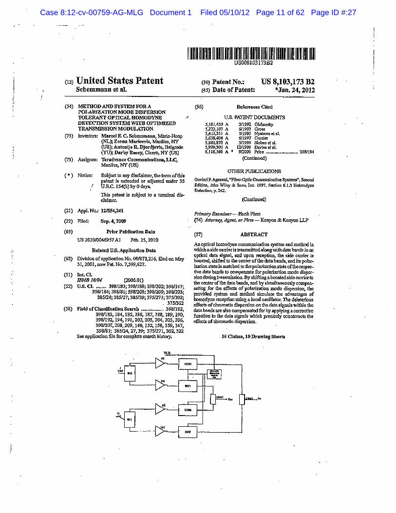
(12) United States Patent Schemmann et al.
(54) METHOD AND SYSTEM FOR A POLARIZATION MODE DISPERSION TOLERANT OPTICAL HOMODYNE DETECTION SYSTEM WITH OPTIMIZED TRANSMISSION MODULATION
(75) Inventors: Ma~el F. C. Schemmann, Maria~Hoop (NL); Zorau. Maricevic, Manlius, NY (US); Antonlje R. Djordjevlo, Belgrade (YU); Darby Racey, Cicero, N'{ (US)
(73) Assignee: Teradvance CommunJcat1ons, LLC, ManliusJ NY (US)
( •) Notice: Subject to any disclaimer, the term of this patent ls extended or adjusted under 35 u.s.c. 154(b) by 0 day~ !
This paten.t is subject to a twminW Ws~ claimer.
(21) Appl. No.: 12/554,241
(22) Filed:
(65)
Scp.4, 2009
Prior Publlcat1Dn Datu
US 2010/0046957 AI Feb. 25, 2010
Related U.S, AppUcaijon U.ta
(62) Division of application No. 09/871,216, filed on May 31,200l,now Pat. No. 7.,599,627.
(51)
(52)
(58)
Int.CJ, H04B 10/04 (2006.01) U.S. Cl ......... 398/183; 3981188; 3981202; 398fl47i.
398/184; 398/81; 398/208; 398/209; 398/203; 385/24; 385/27; 385/39; 375/271 j 375/302;
375/322 Field of Classification Search .................. 3981182,
398/183, 184, 185, 186, 187, 188, 189, 190, 398/192, 194,191,202, 203, 204, 205, 206, 3981207, 208,209,140, 152, 158, 159, 147, 398181; 385124, 27, 39; 375/271, 302,322
See application file forc:omplete search bistory,
llllllllllllllllllllllllllllll~ Ill~ llllllllllllllllllllllllll~lllllllll US0081 03173B2
(10) Patent No.: US 8,103,173 B2 *Jan.24,2012 (45) Date of Patent:
(56) References Cited
U.S. PATENT DOCUMENTS 5,101,450 A 5,222,!03 A S,4!2,35l A 5,638,404 A 5,880,870 A .5,9991300 A G,llS,$66 A •
'3/1992 Oisbansky til J9fJ3 Gross S/1995 Nytrtrom ct al. 6/1997 Crozier 3/1999 Sieben ct at.
12/1999 Davies 1;t al, 9/2000 Pd-;;c ...................... """' 398/194
(Contmuod)
OTHER PUBLICATIONS
Govind P. Agrawal, ''Fiber-Optlc Communication Syst:mm", Second Edition, John Wiley & Son~ Inc. 1997, Section 6,1,3 Hcl:erodyno, Dcicetion, p. 242:.
(Continued)
Primary Examine,-- Hnnh Phan (74) Attorney, Agent, or Finn- Kenyon & Kenyon LLP
(57) ABSTRACT
An optical homodyne communication system and method in which a side carrier is tra:n.snritted along with data bands in an optical data signa~ and upon receptio~ the side carrier is boosted, shifted to thecenterofthedata bands, and its polar .. ization state is matched lo thepolari:zation state oftberespec~ tive data bands to compensate for polarbatlon mode dispersion during transmission. By shifting a boosted side canier to the center ofthe data bands, and by simultaneously compen .. sating for the effects of polarization mode: dispersion, the provid~ system and method simulate: the advantages of hom~?dyne reception using a local oscillator. The deleterious effects of chromatic dillpersion on the dotn signnls w.!tbln the data bands are nJso compensated for by applying a corrective function to the dala ::;ignals which precisely counteracts the effects of chromatic dispersion.
16 Claims, 10 Drawing Sheeb:
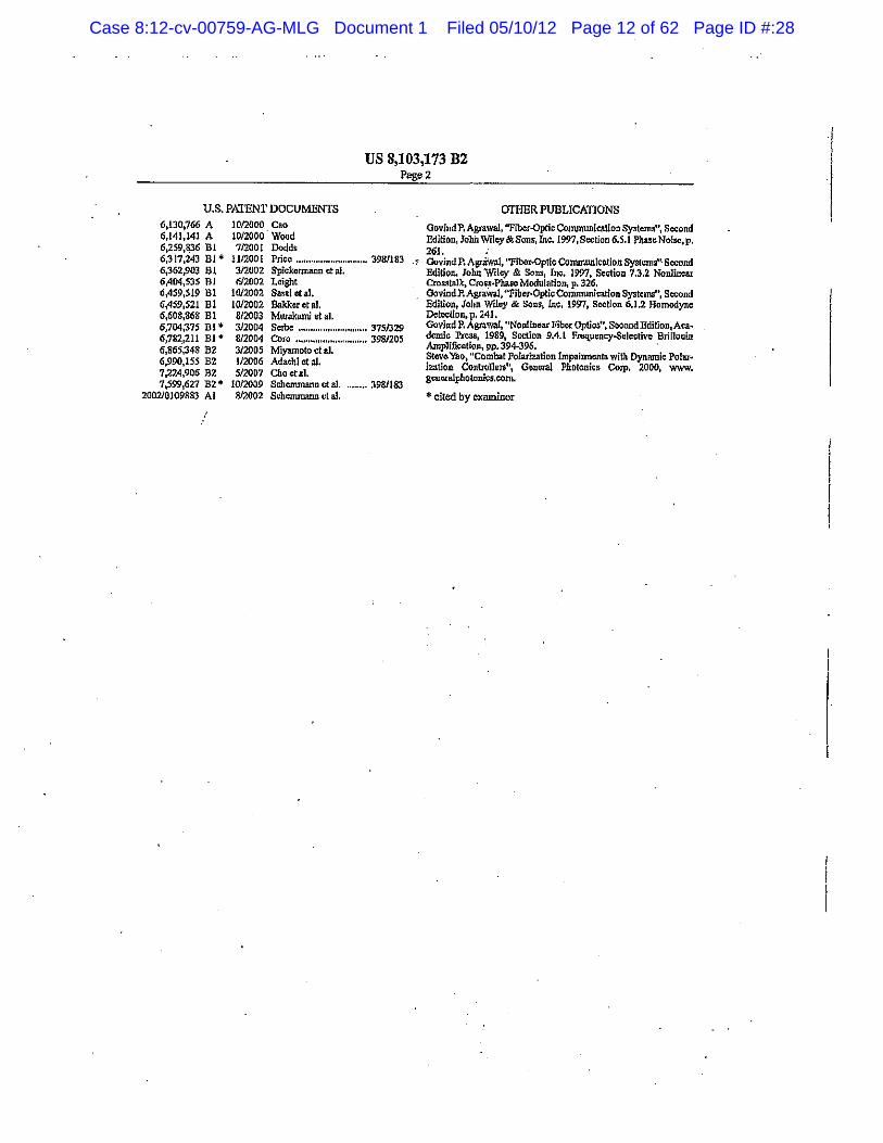
Case 8:12-cv-00759-AG-MLG Document 1 Filed 05/10/12 Page 12 of 62 Page ID #:28
US 8,103,173 B2 Pag,e2
U.S. PATENT DOCUMENTS OTHER PUBLICATIONS 6,130,766 A 6,141,141 A 6,259,836 Bl 6,317,243 Bl* 6,362~03 81 6,404,535 Bl 6,4S9,S19 Bl 6!'159,521 Bl 6,608,868 Bl 6,704,'375 Bt• 6,782,211 Bl • 6,865,348 B2 6,990,155 B2 7,224,906 B2 7,599,627 B2 •
2002/0109883 AI
1012000 Cao 10/2000 · Wood 1/2001 Dodds
1112001 Price"""'"""'"'"''"'~"'' 3981183 -~ 312002 Spickormann et al. 6/2002 Leight
10/2002 Sasal et al. 1012002 Bakkcreta1. 8/2003 Murakami et al. 3/2004 Serbe ............................ 375/J29 812004 Core ••. , .... ., ................... 398/205 3/2005 Miyamoto etal. 1/2006 Adachi et aJ. 5/2007 Cho et al.
10/200.9 Schemmann cts1. ..• - ... 398/183 812002 Schl.'lnJDaUII ct aJ.
OovindP, Agta.wal, "Fiber-Optic Comnnmication Systems", Second Edition, Johh Wiley &Sour, Inc. 1997, Se<:tion 6.5.1 Phase Noise,p. 261. • Govind P. AgriWal, ''Fibar.Optlc Communication 8yslems"· Second Edition. John-Wtley & Sons, Inc. 1997, Section '1.3.2 Nonlb:u:ar Crosstalk, Cross-Phase Modulation, p. 326, GovindP. AgraWal, "Fiber-Optic CommUilicUion Systems'', Seoond Edilion, John Wiley & Sons, Inc, 1997, Section 6,1.2 Homodyne Detection, p. 241. Govind P. Agrawat, "Noulinear Fiber Optics .. , Soco.nd Edition, Academic Preu, 198g, Section 9.4.1 Frequency-Selective Brinoui.n Ampli:fk:otion, pp, 394-396. Stcvo. Yao, "Combat Polarization Impairments with Dynamic Poiarhation Controllen'\ G~oral Photonics CoJP. 2000, www. genocalpltotonics.corn.
* cited by examiner
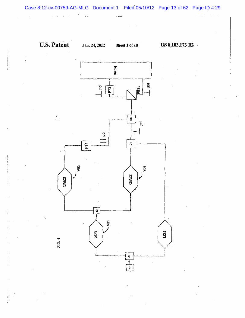
Case 8:12-cv-00759-AG-MLG Document 1 Filed 05/10/12 Page 13 of 62 Page ID #:29
U.S. Patent Jan.24,2012 Sheet 1 oflO US 8,103,173 B2

Case 8:12-cv-00759-AG-MLG Document 1 Filed 05/10/12 Page 14 of 62 Page ID #:30
U.S. Patent .Jan. 24, 2012
FIG. 2a
'i I ., i
::
!
FIG. 2b
I j CH3&4
i { ·.
FIG. 2c
CH1 &2
Sheet2 oflO US 8,103,173 B2
+30G +200
CH3&4
+10G
CH1&2
+10G

Case 8:12-cv-00759-AG-MLG Document 1 Filed 05/10/12 Page 15 of 62 Page ID #:31
U.S. Patent Jan.24,2012 Sheet3 oflO US 8,103,173 B2
Q FIG.3
1;1 +1
-1
-1,-1 1 -1 '
-1 0 +1

Case 8:12-cv-00759-AG-MLG Document 1 Filed 05/10/12 Page 16 of 62 Page ID #:32
U.S. Patent Jan.24,2012 Sheet 4 oflO US 8,103,173 B2
FIG. 4a ., I sc
CH3&4 CH3&4
·10G OG +10G +4DG
FlG. 4b J.,tl sc
CH1&2J. CH1&2.,L CH3&4 II CH3&4 tJ
·•
FIG. 4c J.sc
CH1&l CH3&4 20Gb/$ 20Gbls
-10G OG +'lOG . -t40G
Case 8:12-cv-00759-A
G-M
LG D
ocument 1 F
iled 05/10/12 Page 17 of 62 P
age ID #:33
.•.· .·.·,·.·.•.·.···
ll T~1 LPF1 EOFAe I I ---DWOM3 H":J~ 60GHz • PM BT3
DWOM4 50GHz
FIG.S I I I I
ia-0.
1 !. .fil
,i5' :::1 g 3 "0 (D
"' (/)
~~ "' Ill
~ ?'-l "'C ~ a-a
;<
"' N
·"" "' 0 ..... "'
<7l =-.. $il. Ul <:> ...., ..... 0
g !j¥J ...... ~ 8 ~ to>
Case 8:12-cv-00759-AG-MLG Document 1 Filed 05/10/12 Page 18 of 62 Page ID #:34
U.S. Patent Jan. 24, 2012 Sheet 6of10 US 8,103,173 B2
.-::
/
Case 8:12-cv-00759-AG-MLG Document 1 Filed 05/10/12 Page 19 of 62 Page ID #:35
U.S. Patent Jan. 24, 2012
FIG. 7
EDFA3
input
Sheet7 oflO US 8,103,173 B2
CIRCULATOR 1
20fan Spool <Jf Dillpfrsfon ColftptiUIIfltlng flbai'
OUlPUT
Case 8:12-cv-00759-AG-MLG Document 1 Filed 05/10/12 Page 20 of 62 Page ID #:36
U.S. Patent Jan,24,2012 Sheet 8 oflO US 8,103,173 B2
FIG. Sa
I FIG.8b
FIG.8c
PMD 0,90 DEGREES 0,90Di;"GiiEES corrected
FJG.8d
+26C
AG.Se ili d1 S<:SOO
SHIFTED &a£$G! +~$4
FIG. 8f ffi ~ llC'S 90~ SHIFTED
't~SG
Case 8:12-cv-00759-AG-MLG Document 1 Filed 05/10/12 Page 21 of 62 Page ID #:37
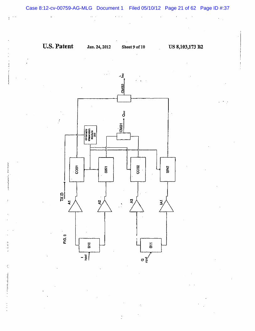
U.S. Patent Jan.24,2012 Sheet 9 oflO US 8,103,173 B2
~ r
3
c'J I ~
"' uc .::; ="· 0 ... "$~
r-1 f-~-~ •o ,.;e
2 z "' "' "' z 1jj 0· 1jj 0 0
l 7\ Y\ 1\ '· Y\
"' <!i L u: 0 1--J ~
1-~ ~
"' "' -~r .5 .,/

Case 8:12-cv-00759-AG-MLG Document 1 Filed 05/10/12 Page 22 of 62 Page ID #:38
U.S. Patent Jan.24,2012 Sheet 10 oflO US 8,103,173 B2
,,
i FIG.10a
outpul
l cap1
w FIG. 10b
-~~ mpul cap1 ~
. ~ r output
Case 8:12-cv-00759-AG-MLG Document 1 Filed 05/10/12 Page 23 of 62 Page ID #:39
J
US 8,103,173 B2 1
METIJODANDSYSTEMFORA POLARIZATION MODE DISPERSION TOLERANT OPTICAL l!OMODYNE
DETECTION SYSTEMWITIJ OPTIMIZED TRANSMISSION MODULATION
CROSS-REFERENCES TO RELIITBD APPLICATIONS
2 SUMMARYOFTHB~NTION
The present invention meets the above objectives by proM viding an optical bomodyne COlllJDUWcation system and
s me1hod in which a reduced amplitude side cattier is transmit-.. ~ ted along with data bands in an optical data signal, and upon
reception, the side carrier is boosted, shifted to the center of the data band!, and its polari7..atian state is matched to the polarization state of the respective data bands to compensate
10 for polarization mode dispersion during t:nwsmission. This scheme achieves the signal-to-noise benefits of homodyne reception without incurring the conventional restrictions and complications ofhomodyne reception such as requlriog tbe
This app1ication is a divisional ofU.S. patent application Scr. No. 09/871,216 filed on May31, 2001, which is related to copending and. commonly assigned U.S. patent application Ser. No. 09/748~750, filed in the United Stlll:cs Patent and TrademarkofficeonDec. 26,2000, entitled "Method, System 15 and Appararus for Optically Transfening Iofonnatlon"J which is expressly incorporated herein in its entirety by ref. erence thereto.
phose of a signal from a local oscillator to be locked to tb~ phase of the optical signal.
According to one embodiment, the present invention provides a method of optical communication tlmt begins wlth providing a quadrature modulated optical data including two data bands separated in :frequency, each dafa band having
/ FIELDOFTHB~!ON 20 in·phati'c:: Wld quadrature components. T.he power of the quadraturemodulatedoptkal data signal ls Umited in oiderto limit non·linear effects by reducing the power of the optical data signa] during transitional states in which data symbols
The present invention relates to optical data· communica .. tioo, and in particular, relates to a method snd optical data communication system tbat improves signal-to-noise ratio of optical data signals, counteracts polarlmionmode dispersion 25 and improves robustness to fiber nonlinenrities.
BACKGilOUND iNFORMATION
transmitted in the optical dnta signnl change in value, und in particular by reducing the power to 7.ero such that transmitted power decreases to zero at approximately the mid poiDt of the transitional states. The opt:Jcal dnta signal is combined with a sidecmicrat a singlefrequencybetw~ the two data bands of the optical data signal and then transJ.njttcd actoss optical
CUrrently, optical data communicntlon systems are being JO .fiber to a receiver. upgraded from a 10 Gbls data transmission rate up to a 40 At the receiver. the side carrier is separated from the two
· Gb/s transmission rate. However, data transmission at 40 data bands of the combined optical data signBI and illcrea&ed Gb/s (or higher) prcsentsexteil!livedesignchallengesbccause in amplitude relative to the duta. 'fhe llide carriers are then the effects ofpolarization mode dispersion (PMD), ·chromatic lihlfied tr;'l the ml.ddle of each oftberespective two data bands, dispersion and fiber non~linear effects such as cross~phase 3S· Since the .rC!alionshlp between the polarization state of the modulation become more dominant at the .higher transmis· side carrle~ and the polarization state of the data bands does sion ratca, In pnrtlcular, the limit of tolerab]e polarization not stay constant during transmission over optical fiber, the made dispersion, usually defined as 14% of the data bit dum· polarization state of the shifted side carriers is adjusted to tion, is only 3.5 ps a1 a 40 Gb/s transmission :rate. A 3.5 ps match the polarization state of the data bands at which tbey polarizatioomodedispersio.n translates to anattainablereru::h 40 are centered. of seveml hundred kilometers over single mode fiber which The present invention further provides a method of com• has a typical :fiberPMD ofO.l ps/km11z. pensatingfortbee:fl'ectsofchromaticdiSpersionduringttans-
CUrrentopticalcommun.lcatlonssystems,suchasthePMD mission over optical fiber by separating the in-phase aod compensation nmmgement described in U.S. Pat. Net. 6,130, quadrature components of the two data bands prior to opt a~ 766 to cao, generally attempt to compensate for. PMD by 45 electric conversion, and, after optoelectric conversion, com-splitting received optical signa1s into x and y mode campo- pensating for chromatic dispemion by applying a corrective nentll having orthogonal polarization, and then adjusting the function to each of the in-phase and quadrantre components delay on one of the orthogonal components to align the of the data band~ the corrective function precis~ly counter-modes. This arrangement requires significant signal process- acting the effects of chromatic dispersion on the in-phase and ing and differential de Jays to cove-r the range of frequencies so qgadrature componcats. carzying data. The present invention also provides a method of providing
NonJinearities inducedduriogoptical transmission are also information concerning a transmission device by providing amplified at higher data rotes. WhUe it is necessary for accu- an optical data signal having data bands and a side carrier with rate detection that optical data slgna1s be atleast20dB above the side carr:lermodul11ted to carry an identification code, the background noise, if the data signals are transmitted wlth too ss identification code including information concerning the much power~ nonlinearities can play a greater role in distort- transmitter. According to an embodiment of the present ing 1he signal. In addition. in coherent systems typical bet· invendon, the information concerning a tmnsu:Uttet embed-enldyne optical reception systems suffer an inherenl 3 dB dedinthes:ldecsnierincludesparam.etecsusedinthecorrec-penalty with respect to homo dyne systems and introduce tlvc function to precisely counteract the effects of chromatic phase noise through use of a local oscillator, and thereby add 60 dispersion. n further level of complexity and constraints to optical system 1u1 optical data signal tiansm:itteris provided for general-design. . ingthe quadnrture moduluted optical data signal including at
What is therefore needed is a cost-effective method and leastonesidecarrier. The=trunsmitteriDcludesaMacb~Zender system that compensates for PMD, optimizes _SNR .perfot- modulatorwbichgenemtes an opfi!;B} car:rWrsigna]by modu-mance and minimizes phase: noilic and nonlincarities associ-· 6!i laling a pair of Iii de cariiero onto an :input optical signa]. The alcd with transmission over fiber at high data traosm.ission optical carrier Signal is modulated by at least two phase rates. modulatOIS which modulate a pair of data sigwds, in quadra-
Case 8:12-cv-00759-AG-MLG Document 1 Filed 05/10/12 Page 24 of 62 Page ID #:40
US 8,103,173 B2 3 4
ture, onto thuopticalcarriersigmtl, outputting an optical data PIG. Sh shows the spectrum of an optical carrier signal at sigualincludingatleasttwo data bands. By spreading the data the outputoftheS7 ofPTG. S according to an embodiment of b!lD.ds onto the pair of side carriers1 the amplitude of the the.present invention. optical data. signal is :reduced to :zero during transitions . FIG. 8c shows the spectrum of an optical carrier signal at between data symbols. The transmitter nlrso Includes a second s 1he output of the PBS3 ofFIG. 5occording to an embodiment MacP,-Zender modultitor which imprints a low-frequency 1X.~ of the present invention. JD (tmnsmitteridentification code) side cwrler.onto the input PIG. Sd shows the spectrum of an optical carrier signal at optical signal. The TX ID signal side carrier then coinbincd the output of the SSl of FIG. S according to an embodiment with the optical data signal fortran~mission. The transmjt1ed of the present invention. identification code includes information concerning 'the to FIG. 8e shows tlle spectrUm ofao optical carrier slgnal at trans111ittcr, such as its location) from which the distance theoutputoftheCSofFIG.Saccotdingtoanembodimemof between the transmitter IUld a receiver may be deduced, the present ioventian,
Theprescnti.n.vcntlonfurtherprovidese reccivc.rforbnplc- FIG. 8fshows the spectrum of an optical carrier signal at the output oflhe C6 of FIG. 5 according to .en embodiment of
menting homodyne reception, The receiver includes a sidQ 15 the present invention. cllllier boosting module for ln.creasing the amp1itude of the PIG. 9 is a block dlagrwn of a chromatic dispersion com-side cani~relativeto.thedata ban~dein tJu:optiC:Sl~tasiSJld all. pensation circuit according to au embodhnent of the present The recewer further 1ncludes a Sl earner sbiJ.lmg mo u e invenlion. coupled to th,e side cani~r boosting modu1e which shifts the FIG. lOa is a block diagram of a mlcrostripimplemenlation side carrier :lnto two shifted ~riers. Each of fue sbifted 20 of a circuit that nppHcs a COS transfer function to an input carriers is shifted to the center of one of the data ban&. In signal according to an embodiment of the present invention. addition, means: for compensating polarization mode dlsper- FIG.lObjsa blockdiPgram of a micmstrlpimp1emeqtation sian that are coupled to.thesidecarriershiftingmodulematch of a circuit that applies a SlN transfer function to an input tbepolarizatlon states of the shifted carriers to the data bands signal accon:ling.lo on embodiment of lhe present invention.
D!l'll\lLED DESCRIPTION by adjusting eitherthe polarization state ofthe shifted carriers 15 or the polarization state oftbe data bands. After optoelectric conversion of the optical data signal1 tbe receiver employs a chromatic dispersion correction stage that includes circults J.Tmns.mlssion that apply transfer functions to the in-phase and quadrature Inacco:rdance wilh the present invention, at a transmitter, a detected data channels 3D pair of side cDrriern ia modulated onto each side of a mono-
BRIEF DESCRJPTJON OF TilE DRAWINGS chromatic opticnl canier signal, which is tbe.o split into two channels. Bach optical carrier signal tlbnnnel is modulated with two 10 Gbls data signals in an orthogonal phase rela-
FlG. 1 is a block diagram of a transmitter according lo an tionsbip to one another. The data signals !Ire spread onlo the embodiment of the present invention, J~ two side carriers in each channeJ, and in effect, fll'Cizpread out
FlG. 2a shows the spectrum of an optical carrier signal al by fifty percwt ln the frequency domain. This spreading is the output ofMZl of FIG. 1 nccording to no embodiment of equivalent to multiplication by a sine wave at half the data the present invention. mto, and results in each data symbol returning to zero
FJG. 2bshows the spectrum of an optical data signol at the between transitions, refened to as quadrature-return-to-zero outputofQMZ3 ofFIG.l afterda1aiu.odula1ioninquadrature 40 (QRZ). Using QR~ the ]lOWer of the optical data signal is according to an embodiment of the present invention. madeindependentofthe data patter.o.. Thepolari~tionofone
PIG. 2cshows the spectrum of au optical data signal at the oftbe optical data signal cbannels is tbensblfted1 and one of output ofQMZ2 ofFIG.l according to an embodimont oflhe thechannelll istlomblned with a channeloftheorlghmlmono-prerent invention. chromatic canier that has been modulated with a traruunis-
FIG. 3 shows a lOG symbol per second QuadratureRe1um 45 sian identitictltion crurier of less than 100kHz. to Zero (QRZ) constellation diagrum of the output from The tWo optical data signal bands, whlcb each cany a 20 QMZ2 and QMZ3. Gb/~ data stream, are combined and either multiplexed with
FIG. 4a shows the spectrum of an optical dala slgnal at the adjacent channels at siiDUar .frequency and orthogonal polar-output of Cl of FIG.l according to an embodiment of the izationoroneofthotwocbannelsisshlftedinpolarmttion to present invenllon, . so match tho ~ther chaooel, In either case, the optical dala slg-
FJG. 4b shows the spectrum of au optical data signal at the nals are; mUltiplexed according to a D!':nse Wave Oivision output of CZ of FIG. 1 according to an embodimeot of the Mulitplexing (DWDM) scheme and transmitted along long present invention. haul fiber 1o a destination receiver.
FIG. 4cshows the spectrum of an optical data signal at the FIG.llllustrates anembodimentofa transmiuer oocording output ofthe DWDMofFI0.1 according to an embodiment 5~ to the- present .invention1 which may be implemented on a of the pr~sent invention. Uthiurn~Niobate chip1 fotexamp1e.Anoptical signal genera-
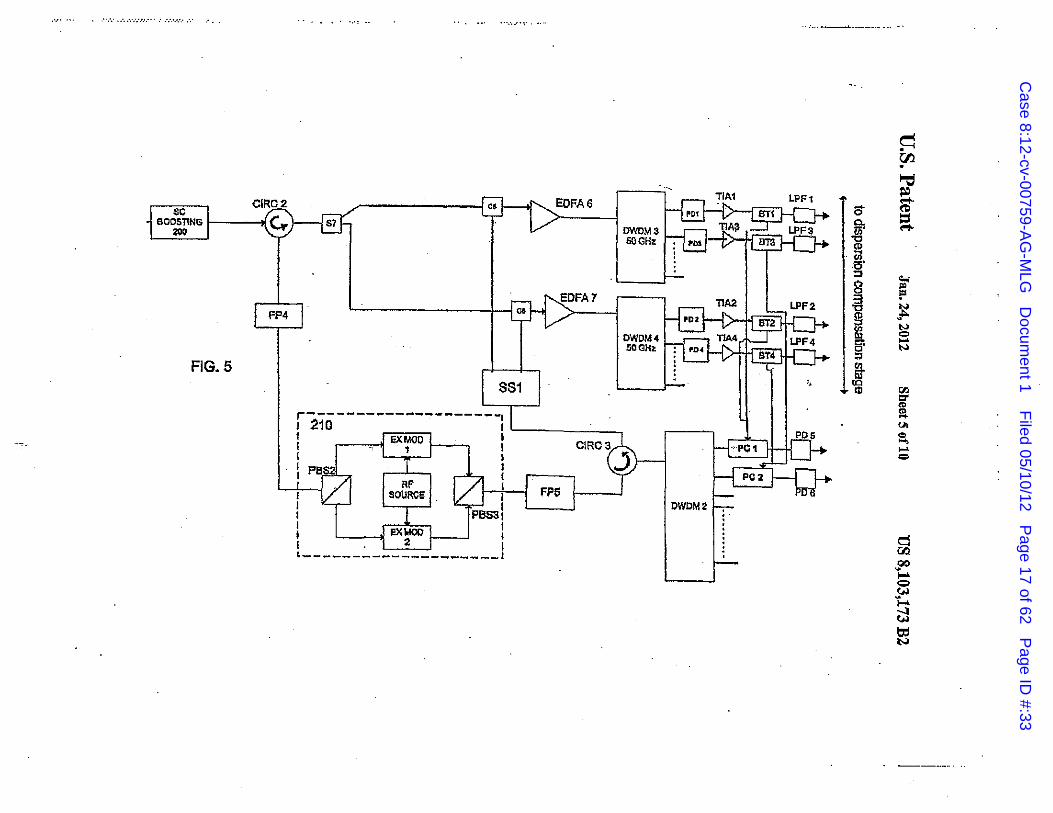
FIG, 5 is a block diagram of a receiver accordlng to an tor SGI, whlch may be a.Iaser1 generates a monocllromatic, embodiment of the present invention. polarized optical carrier at a reference frequency wWch for
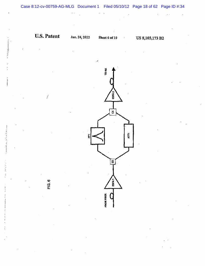
FIG. 6 is a block diagram of a fitst embodiment oflbe side purpo~cs of tho following discussion js designated as the carrier boosting module aecordingto the present invention. 60 origin (0 GHz) in terms of relative frequency. The optical
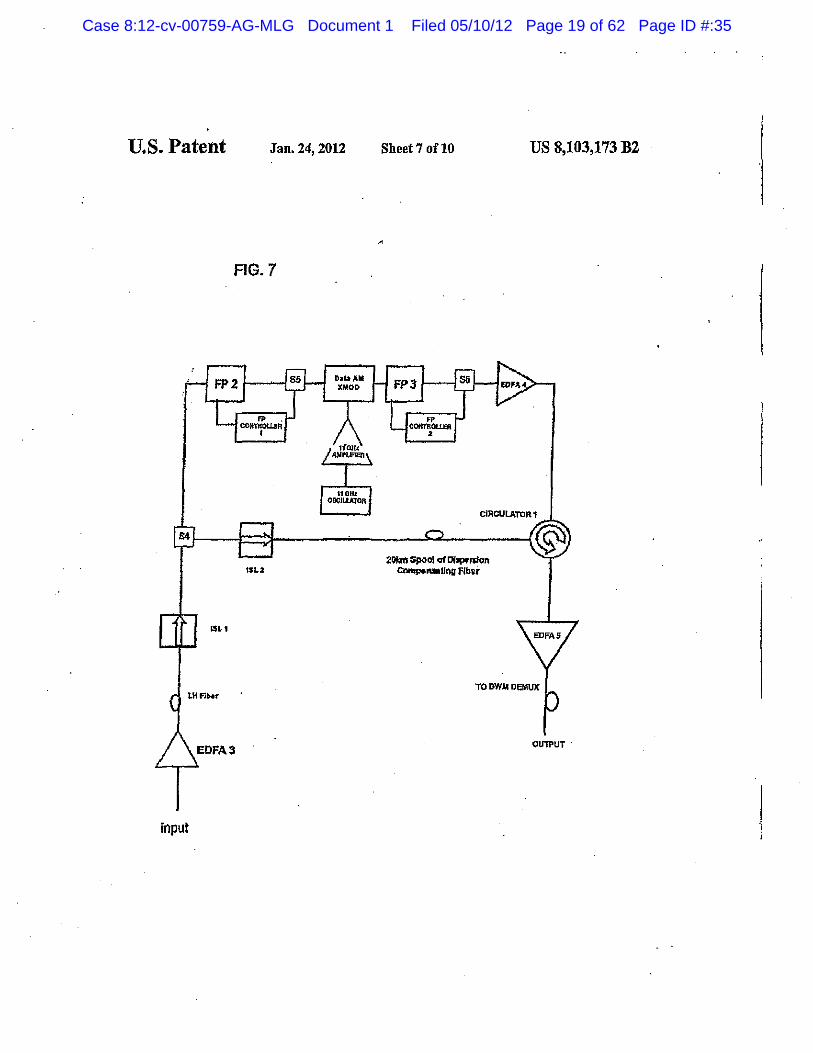
FIG. 7 is n blockdiagnun ofn.second embodiment of the signal is thereafter split into two channels, an upper cbnnnel side carrier boosting module nccordinS 1o tbe present inven- going to Mach-Zender modulator MZ1. and a lower channel tion which employs the Stimulated Brillouin Scaltering bt:ingtransmitledtoMacb-ZendermodulatorMZ4. Thedivi· (SBS) effect, . sionofliglltin1ensity between lbe two channels can be uneven
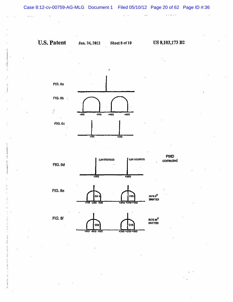
PIG. Ba shows the spootrum of an optical carrier signal at 65 wilh the lower channel receivin& fort~Xumple,ju:;t 10 percent the outputofthc FP4 of FIG. 5 according to an embodiment of the light intensity generated by SGl, At narrow-band of the present invention. modulator MZ4, the lower channel of the optical signal is
Case 8:12-cv-00759-AG-MLG Document 1 Filed 05/10/12 Page 25 of 62 Page ID #:41
US 8,103,173 B2 5 6
modulated with a "'Ihmsmitter Identification" ('IX ID) tone ABean be discerned, the i>peclnlm includes data channels 1, 2, in the frequency range of 10KHZ to 100 KHz above the 3 and4in bo1hlowerandupperdata bands. Channels land2 reference frequency. At modulator MZl, two sets of side are in perpendicular polarization and channels 3 and 4 are in carriere: at +/-?.0 GHz and +l-30 GBzare modulated onto the parallel polarization.Thereference~rrleratapproximately 0 optical sigoal. The spectrum for the modulated signal, s GHz from MZ4 is in perpendicular polarization. denoted an optical carrier signal
7 is sbown in FIG, 2a. As~, Accorilingtotbe iUustrnted embodiment, the output signal
shown in the figure, the resulting spectrum output from MZl from C2 Is input to a polarization beam splitter PBSl whleb shows four peaks, two below the reference frequency at -30 splits the signal into perpendicular and parallel polarized GHz and -20 GHz relative to the reference frequency, and components, thereby separating the data channels 1 and 2 two above the reference 'frequency at +20 GHzand +30 GHz. 10 from cbWlllels 3 and 4. The perpendicular component (con-
Th I MZl · • h li · tuining data channels l and 2 as well as the centrnl reference eoutputofmodu ator JS ,urt ersp t mto an upper :frequency)is111Uls:m.ittedalonglowerpatb 102 to a first chan·
channel which is tracslllitted to quadrature data modulator neJofadenscWE\'YodivisionmultlplexerDWDM, the parallel QMZ3 and a Iowercharulelwhichistransmitted to quadrature component (contnin.ing dot a cluuulels 3 and 4) is input to n dam modulator Q:MZZ. Data modulator QMZ2 imprints two 15 po1nrization tmnsformer PT2, which rotate !I' the polarization individUal lO Obis data streams in quadrature (in orthogonal ofthepamllelcomponent back into aperpendioularstatl;), Tho phase relationship) CH.l and CH. 2 onto each of the pairs of output from PT2 is then input to a Gooond DWDM channel. side carriers above and below the reference frt:qucncy. Simi- Each DWDM channel acts as a band pass filter and passes lnrly, data mqdulntor QMZ3 imprints individual I OGb/s dntn onlyfreqnenciesthatfal1withina SO GHzband.Assumingfor streams CH.3 and CH.4 onto each oftbe pairs of side carriers 20 illustrative purposes that DWDM channell passes :frequen-in 1he optical carrier signal Respective bias control elec- "ie:;; from -50 GHz to 0 GHz relative to the reference fro-trades VB2 and VB3 assist in keeping the dnta streams in quency, and DWDM chanool2 passes frequencies :from 0 to quadnlture. Spectra oftbeoutputs:from QM~ B.Dd QMZ2 are +50 G~ data channels 1 and 2 ore passed ooly in the data shown in FIG. 2b and FIG, 2o respectively. As can be dis- band from -40 GHz to -10 GBz and while data channels 3 cemedinFIG. 2b and FIG. 2c, the output spectra from QM23 2S and 4 ro"O passed ooly in the data baDd from +l 0 GHz to +40 and QMZ2 show two data bands, one extending from -40 GHz. The DWDM multiplexes eaoh oflhepa&sed bands onto GHzto -lOGHzandanotherextendingfrom+lO GHz1o +40 a long haul fiber (notshown), The output &pectram ftom -50 GHz relative to the reference frequency. GHzto+SO GHz outputfrom the DWDMisshowninFIG. 4a,
By imp.cintiDg two 10 Gbls data streams jn qu11drature, in Tho adjacent DWDM channels each pass 20 Gb/s of data, effect, 20 Gb/s of data ara modulated on1o each pair of side 30 combining for a totlll of40 Gbls. carriers (-30, -20 GHzand +20, +30 GEz, respectively) and ln an altemntive embodiment, apolarizntion multiplexing each 20 Gbls data band covers 30 GHz ill the f!equency scheme may be used, making it unnece!lSary to separate data domain. By providing two side caniem, with orie sido canier channels 1;ood z from data ~els 3 and 4. As described in inlbepairaclocknrteaway:fromtheother(i.e.,30GHzbeing related and_commonJy OWJled application [Scr, No. 091782, a clock' away from 20 GHz),the data bits in both I and Q 35 3S4]herebyin<:orporatedforreference,thepairsofdatachan-format are multiplied in tb.etimedo.main by a 5 GHz sinusDid nels can occupy the same data band iftheirpolarlzationstates which crosses zero every l 00 ps. Thus, the total data signal remain orthogonal and ~s do JJOt interfere wilh each other. always crosses through zero in between any pair of symbols In thisimplementatioD, thepolmizationbeam splitter PBS1 is (anypairofi,Q data), referred to as quadmture-return-to-r.ero not needed and the output from CZ can be sent directly to one (QRZ) modulation. 40 of the DWDM input ch11nne1s.
FIG. 3 illustmtes the key property of the QRZ format, D. Reception showing that the trajectory between two successive symbols In accordance with the p:resent it:wention, a bomadyne always leads through thel·Q origin. Baob comerofthe figw"e receptipn sys1em is employed to receive the optical data s:lg· represents apairofl,Qdatasymbols (e.g.,l=l,Q"'-1 orl=-1 1 nal generated as described above. Upon rCceptlon, the trans-Q=l). As shown, to get from adjacentcomerpoin~ l=l, Q=l 45 mined side carrier at the reference frequency Is boosted to (upper right comer) to 1=1, Q=-1 (lower right corner) the increase tbe signal-to-.noise ratio (SNR) of the opticnl dntn optical data signal must travel through the origin (0,0). Dur- signal andtocompensatefortbeBttenoationoftbesidecarrier ing eachtmjectorythroughfueorigin, thepoweroftbesigMJ, in the transmitter. The boos1ing of the side carrier increases which is proportion to the square of its amplitud~ goes to the SNR because of the implementation ofhomodyne recep .. :z:ero, so tion in whlch overall detected sigml power is incrensed in
Returning to FIG. 11 the output from. modulator QMZ3 is proportion to1hepowerofthe local osciUator, orin the present input to a polarization transformer PTI, whlch shifts the oase(aswjl]beciiscuss,dbelow).tbetransmittedsideeanier. poladzalion of tho optical data signal output from QMZ3 90 Once the 11inplitude of the side canier ,power is boosted degrees. The polarization of the signa] oulput from PTl is relative to the transmitted data bands, the side carrier is arbitrarily lllustrated by parallel lines as pamllel polarization ss shifted by +1-25 GHz into two side carriers that are each as opposed to a perpendicular polari:z:ation of the original shifted to the center of one of the two data ·bandS' to further optical signal. FUllhermore, the output optical data signal implement bomodyne reception. from modulator QMZ2 is combined at combiner Cl with the After the: shifting of the side carriers, the twa side carriers TX lD pilot signal from MZ4: The output from Cl is shown are separated and then modified by polarization controllers in FJG. 4a.As noted above, the intensity of the TX ID signal 60 wblch match the time-vacying polarization State of each the is reduced in comparison with the opticnl data s!goo] :froin sldeeanierstothedifferenttime-vnryingpoJnrizationstateof QMZ2. It is also no1ed that the polrui11rtion of 'the output the respective dam bands, thus overcoming the effects of· signal from Cl is shown as peipendicuh~r, since lbe polariza- polarir.atim1 mode dispersion by controlling the polarization tionoflhe outputftom Cl remains unchanged from theorlgi~ at oDly a siiigle frequmcy, . nul polarization. Thereafter, the output signB] ftom PT1 is 65 -Accordi:Dg Ia an embodiment of tho presenl invenlion1 a combined with theoutputsigool ftomcombinerCl at~. The chromatic dispersion compensation stage ia used to counter spectrum of the output sigaal out ofC2 is shown ln FIO. 4b. .J tho effects of disporsion during transmission over Jong b.anl
Case 8:12-cv-00759-AG-MLG Document 1 Filed 05/10/12 Page 26 of 62 Page ID #:42
US 8, I 03,173 B2 7 8
fiber. Since the effects of dispersion can be modeled a& a GHz signal onlo the side carrier. The spectrum of the output transfer function that is; applied tothel and Q data signals, the from the modulator XMOD 1 thereafter contains the refer-chromatic dispersion compeosaliOll stage applies a comperi· enoe frequency and two side frequencies located 11 GHz both sating c;orrectlon function that effectively counteracts the above and below the reference frequency. This output signal transfer function, rendering the I and Q data sisna:ls into their s is then transmHted to another resonator FP3, which is original non-dispersed slate.
1 adjusted byFP controller 2 to center on (and pass) only the
FIG. 5 illustrates an embodiment of a homodync receivei side freq_uency 11 GHz above the reference side carrier fro-according to the present invention. An optical data signal is quency. The res\llting signa~ carrying substantially a single received first by a side carrier boosting module200 forwbich frequencyatthe.refece.n.cefrequency+11 GBz. is amplified in the present invention provides two exemplary embodiments. 10 optical ronplifier BDFA4 and then input to 9irculator CIRCl. In a first embodiment of the side carrier boostlngr~odulc, The circulator passes signals in a counter--clockwise direc-shown in PlG. 6, the optical data signal is first input to an tion. More specificaUyJ CIRC 1 passes the output from optical amplifier BDFAl, which may be. for example, ~n BDFA4leftwardsinacounter-e!ockwisorotatlontowardsthe etbium-dopcd fiber amp1ifier (EDPA). It is noted thllt all outputofop,ticalisolatoriSL2.Itisnotedthatthesidecotrier further optical amplifiers used in the impleme.ntntions lS boosti.ngschemeisalsointendedbeusedincoJijuncUonwitb descn'bed below may be implemented as erbium-doped fiber a dense wave division multiplexing scllcme. Thus, the side amplificiB, The,optical amplifier BDFAl amplifies the entire carrier boosting module can simultaneously process and speclnlm of the received signal by, for exampl~ approxi- boootapluialityofsidecarriers~pacedinftequencyaccord-mately 15-lS.:eB. Thl' amplified signal output from BDFAl is ing to ITU cbaonel spacing. split at 83 between an upper branch that is coupled to a 20 Simultaneously,theopticahignalintbelowerbranchfrom Fabcy·PerotresonatorFPl and a lower branch that is coupled splitter S4 is transmitted through isolator 1SL 2 and then to an attenuator ATfl. meets with the opticai signal from the upper branch output
The Fabzy Perot resonator FPl function$ as a high-Q filter from the circulator cm.c I. This collision of the two optico.l that nearly completely filte.rs out all frequencies excepts for a signals traveling in opposite <fuections generates the SBS series of :frequencies that are separated by, for example, 100 2S non-linear effect, According to One implementation, the fiber Gbz which, nccording _to the International Teleconununica~ connecting isolator ISL Z and circulator CIRC 1 can be dis-tion Union (ITU) grid, is the amount ofbandwldlh allocated persian compcosnting fiber which, due to Its relatively for each channel. The xesonator FPl is adjusted to pass tho smaller cro.ss~eeti:on, promotes higher intensity aod more side carrier at the reference frequency and filter out the data · pronouncednon-lineareffects such liS SBS. When the optical bands of the QPticnl data sigoal.lt is noted in thls regard that JO data signal containing the reference side canier co11ldes with it Is contemplated tl1ot the embodiments ofthepresenthwen- the 11 GHzsidefrequencysignalfromCtRCl, a narrow band tion be used. In the context of the 111! grid, and that the incl'lldingtbesidccnnierintheopticaldatnsignallsamplitled reception approach described allows for simultaneous pro- Jelative to the data bands due to the SBS effect as explained cessing of side c&rriers for a plurality of ITU grid-spaced above, llis moilified optical data signal then reaches the
.t channels. The lower bnmch passed to ATII, which contuin'S 35 circulator CIRC 1 from which it passes in the counter-clock-both the data bands and the ride canier is attenuak:d. The wlso tlirection to optical amplifier EDFAS, which amplifies signalsoutputfromFPlandATilnreCombinedincombiner the entire spootrum oft!J;e modified optical data signal by C4 and then passed to a further optical amplifier EDFAZ 15-18 dB. Theomput :from BDFAS is the final output of the where the combined signal is again amplified by, for example, second ombodlment of the side carrier boosting module: 200. approximately 15-18 dB. Because the side carrier was iso-- <10 Returning to FIG. 5, the_optical data signal output :from the lated and boosted in PPl and the data bands we~ attenuated side ro:arrier boosting module 200 is input to circulator CIRC inATTl, tbe combined signal contains a sklecarrlerboosted 2, which in turn transmits the signal in a counter-clockw3se atlea11t lOdB in amplitude .relative to the data bands, :. , direction toFabry-Perot:resonatar FP4,having a free spectral
A second embodimentoftheside caaier boosti.O.gmod.uJeJ .mnge (FSR) oflOOGHzand finesseontbe orderof1000, The which advantageously makes useofthenmplitude·_enhancing 4S :resonator F?4 is 8!sl) tuned to select the sldo carrier at (ap~ effect of Stimulated Brillouin Scattering (SBS), js shown in proxim_ritely) the reference frequency (0 GHz). FIG. 8a FIG-1. The SBS effect causes a first optical slgnal having shows a spectrum of the signal output from FP4~ indicatlng oarrow frequency band aroUnd frequency X to be amplified tl\at the daiu bands have again been filtered out. The data when collides with a signal of :frequency X+ ... 11 GHz"tlavel· bands that are filtered out at FP4 are resent back toward ingi.ntheopposi"Wdirectio.n. Referrj.ng to FIG. 7, 1hen:ceivecf so c::imllator ClRC 2} where they are-redirected in a coun.ter-sig:nal isinputto optical amplifierEDFA3whichamplifiesthe clockwise direction towards splltter S7. The spectrum of the entire spectnun of the Input sigual. The signal output from output from splitter S7, which includes the two filtered data amplifier EDFA3 is tmcsmitted to optical isolator ISL l, bandsot -40GHzto -10 GHzand+lO GHzto +40GHZ;. is which permits optical signal to travel only in one direction shown in FIG. 8b. (the dire<;tion indicated by the a:rrow ln the figure) and pre- $S lt .is noted lhat when tbe optical data signal is transmitted vents optical signals being reflected or transmitted back over long haul fiber between the transmitter and the receiver, toward the amplifier BDJ1A3. From 1he optical Isolator lSLl, the polarization state of the transmitted signal is scnunbled, the optical data signal is split into two branches at sp1itterS4. with the result that the received liignal has an unknown time-
A first upper branch from splitter S4leads to Fabry Perot varying polarization state. Since the time-vmyi:ng polariza~ resonator FP2, which passes the side canier(e.ndotherm_odes 60 tion state varies with frequency, the side carrier is expected to ill the series of frequencies) in between tbe data bands. FP have a differentti.me-varyingpola.rizationstmethnnehherof controller 1 outomntically ndjusts tberesonntor FP2 so that it the data bands because it is sepnratedfrom the centerxofdata concctly passes the side carrier using input from spliUer SS bands by 25 GHz. When theoutput:from resonator FP4 is ±ed aDd filters out the data bands. The output from FP2 is deliv- to 1he side <.."Wlier shifting module 210, the side carrier's ered to external modulator XMOD l, whlch elso receives an 6S orthogonal polarizutioD states are split in polarization beam 1"1 OHz signal ftom a 11 GHz oscillator through an 11 GH:z sylittcr PBS2, aDd then each of the orthogonal signals are amplifier. Thcwctc:rnalmodulatorXMODlmodulates tbe 11 11eparately modulated by25 GBzinXMOD 2 andXMOD .3,

Case 8:12-cv-00759-AG-MLG Document 1 Filed 05/10/12 Page 27 of 62 Page ID #:43
US 8,103,173 B2 9 10
rC$pectively, and then joined back iJI PBS3. The output from as baving 8 single polarizalion, und then maWhing to tbe PBS3 is ilJU$tmted in FlO. Be, which shows two side carriers polarizntion oft he side carrlcr. at -25 GBz and +25 GHz from the reference frequency, RetumingonceagaintoFIG.S, thepolarl:zationcontroUers respectively. The output from PBS2 is passed on to FabrY· . PC 1, PC 2 output polatization compensated side carrier Perot :filter FPS (FSR=SO '<H-:Iz, fiuesse >SOD) which passes 5 signals lo circulator CIRC 3, from wWch they are forwarded both the 25 OHz left and right. shifted side carriers, and.$ to splitterSSl. The splitterSSl also shifts tbepbaseofoneof transmitathem to circolntorCIRC3. Circnl.atorCIRCJ deliv· the output branches by 90 degree.<; relative to other branch. ers shifted SC's to reflectivepolarlzationcontrollersPCl, PC The output spwtrum front SSl is shown in PJG. Sd. These 0 2, through respective adjacent 50 GHz-spaced channels of degrecand90degreephaseshlftedcaniersarerecombinedin WDM demulliplexer DWDM '2. The polarization controllers 10 combiners C5 and C6, respectively, with the data bands out-PC 1, PC Z are co!lStructed to provide control of the phase of put from splitter S7. In-phase (0 degree abifted) and quadra-the ~ignals reflected .from the pol_arizationcontroUers back to ture (90 degree-shifted) signal apectrums out of outputs of tho demultiplexer DWDM '2. Such control may be used, for respective combiners CS and C6 are shown io FIG. Be and instance, in order to compensate for the effective fiber length 15 FIG. 8f.As can be discerned, In each spectrum, a side cattier between the polarization controllers PC 1, PC 2 and the is posltioned in the center of a data band. Each side of the demultiplexer DWDM 2. In one implementation, 1he polar- spectra is equivalent to a spectrum generated by a wnvea-ization controJlers PC 1, PC 2 include minors and piczocloo- tional homodyne system in which the local oscillator fre-tric actuators.to adjust the distance the reflected signal tmve1s, quency is matched to the center frequeru:::y oftbe dnta band. which:inturricontrolsthepbnseofthereftectedopticalsignnl. 20 Furthennore, as in conventional homodyne reception, the
Each polarization controller PC 1, PC 2 is used to trans~ power of the central canier frequency is boosted relative to fonn the time-varying polari2ationstate ofoneofthe two side the data ·portion in order to the improve s3gnalvto-noise ratio carriers so that tho polarization states of each side carrier of the detected signal. 'The side canierthat has been shifted 0 matches the time vatying polarizatio11 state of1he respective degrees can be used to d~tect the invphase Q) 10 Gb/s data data bands which ace centered at the side carrier (-2:5 GHz 2!i channels from tlw transmitter (channels 1, 3) and the side and +25 GHz). To accomplish this, each polarization control~ cwricr·tbat bas been sbifted 90 degrees can be used to detect ler PC 1, PCl obtains feedback from the -pholodiodes that the qtnulratun: (90 degree shifted) 10 Gb/s data channels receive the data bands. PC 1rcceives the feedback via bias-T (channels 2, 4). couplon; BT 1 and BT 3, while fC 2 receives feedback via The combined signal from C5 is sent through optical bins-T couplers BT 2l1Ild BT 4. As will be described below, JD amplifier BDFA6 and the combined signal from C6 is sent thedemu11iplexersatthetopofFJG.s;DWDM3,DWDM4t through optical amplifier BDFA7 to final SO GHz spaced receive both the data bands and tbe side canie111, filter them demultiplexers DWDM3 and DWDM 4. Each of the demul-into sepamte, adjacent f~quency channels and then· elfec· tiplexexs DWDM 3, DWDM 4 separate. the data bands and tively multiply the side carrier and data bands together at side carriers, in adjacent channe1s forelectro-opticconversion photodiodesPD1,PD21 PD3 andPD4 (andotherphotoctiodes·. 35 at photo diodes PD1, PD2 and PD3, PO 4 respectively. ln. this ofadjacentchannelsthataronotshown)whichrespdndtothe llllUlDCr 10 GBJs data cha;mels 1 and 3 lU'C separated ln .intensity of the signal (i.e., the squareofthe amplitude). The DWDM 3 nnd 10 GbJs chimnels 2 and 4 are separated in product signal output from thephotodiodesis delivered to the DWDM 4, resulting in the output of four separote 10 Gb/s respective polarization controllers PC 1, PC 2 via bias-T data sighals. couplersBTl,BT2JBT3andBT4.TbeoutputsfromBT1 40 In an imphmumtation aftbe receiver according to the and BT 3, which contain converted data signals 1 and 2, presentinvcnlion, Iow·bandwidlhphotodio!lescanbepluced corresponding to data channels 1 Md 2, are combined to at reflective ends of polari2ation controllers in each leg of provide feedback-to polarization controller PC 11 and the WDMdemultiplexertoprovklemonitoroutputsproportional outputs from BT'l andBT 4, which contain data signRls 3 and to fluctuations in each of carriers, forexamplecaused by cross 41 corresponding to date channel II 3 and 4, are combined to 45 pbase modulation (XPM). Since the resp~tive 10 Gb/s data provide feedback polarization controller PC 2. Jt is noted that channels corresponding to 'the side carrierw generally fiuctu· the data signals land 2 are expected to have a similar polar- are in sympathy, the effect of canier fluctuation can be izationstatesince, during transmission, they oceupytbe same removed if 1llc monitor output fluctuatioM are subtracted frequency range. Equally, datasignab 3 and 4, corresponding from the outputs of the respective received 10 Gb/s output to datu channels 3 and 41 are e:<)lected to have a similar 50 channols. polarizatioo state. At the polarization controllers PC 1, PC z, After the converted data signals are further processed the time-varying polarization of the combined product sig.. through trans-lmpedanceamplifiezs TIA1, TIA2, TIA3, TIA nals are compared to 1he polarization state of the individual 4and low pass filters LPPl, LPF2, LPP3t LPF4, they arc input side carrier !rlgnals. . to a chromatic dispersion compensation stage .shown sche-
By continually IJdjustiogthepolarlzationofthe side carrier ss matically in FlO. 9. It ls noted in this context that the disper· signal and then comparlog 1hc lDodified -polarization state to sian compensation stage can equally be implemented at the the combined product signals, the polarization controllers PC qundraturedutl! modulatol'l! on the tnmru:nitterside instead of, 1, PC 2 can accurately match the time-wrying polarization or_in addition to, implementation at !be rooeiver. The effects state of each of the side crurlers with the timeo-yazying polar- of fiber-induced chromatic dispersion on quadrature-modu-izationstateofthe co11esponding dat& bands. Thls technique 150 lated sinusoidal data signals can. be described by the fblloW· rokes ndvnntnge of fact that it is easier to adjust th13 single ing matrix equation: polarization stare of a single side canier frcqucmcy tban to · adjust the multitude of polarization. states of a band offte~ . quencies, for el'tample, a 20 GHz daltt band, via wide-baml polarization compensation. However, polarization mode dis- 65 penion compensation can nlso beped'ormed here by adjust·, "'· ing the average -polarization of the data band, which iStreate'd
[ J...9Ul\D; 4:/> I=[ C?s;Ho.,., n Qnr,tJl(D, t ... n I[ umn I Q..ovi(D, 4 f) -rinr/il(P, L,/) 1;0s¢'l(D, L. n Q.Jl(f)
(l)

Case 8:12-cv-00759-AG-MLG Document 1 Filed 05/10/12 Page 28 of 62 Page ID #:44
I ·:
US 8,103,173 B2 11
where r_out(f) and Q..oul(f) are frequency domain represenM lations of output I and Q signals~ which are modified from frequency domain representations of input l and Q signals, Un(f) and Q_.in(f), by the dispersion matrix., for whlcb
(2{
D denotes the fiber dispersion in units ofps/nm*km, L stands for fiber length in meters and fstands for frequency in Hz.
The dispersion matdx can be interpreted as a transfer:func .. tion which applies a clockwise rotation angle that is proportional to the square ofthe frequency oftbe transmit1ed sinusoid. Tocountertbcdhlpersion effect, it is feasible to apply an inverse transfer :functio~ which can be interpreted as a counterclockwioe rotaOon, also proportional to lhe square of the frequency, TJ;rls counter-dispersion, or correction fUnction may be descfibed by the following matrix equation!
. [cos(~l(D, L., /)) -tdo(~l (D, L, f)) J dlsp.sgll(D, !.,/)= sln(¢1{.0, £. /)) oos(;J(D, L,fl)
Therefore to correct the l and Q data signal for the effects of chromatic dispmion, the oorreotion function is applied to the l and Q input signals (again, either at the transmitter or at the receiver, as is shown). Multiplying the correction function by the input signals yields:
l_out-coc Clll{D,LJ)-J_in-dn .P I(D,LJH?.Jn
(4)
12 kHz. is received al ~hepolari7.alion cunlrolle.rs PC 1, PC 2and cohverted to the RF domain at pbotodetc:ctors PD3 and PD4. The TX pilots may be coded by frequency m(lduJation or by another code modulation technique, The TX ID identifies the
5 particular transmitter sending tbe signal. allClwing lnfonnation, such as the Jengthof optical fiber between the transmitter and the receiver (which is the "Same as the parameter, L, used m the dispersion correctionfunction), 10 beextmctedftom tbe coded signal. This info):lll8tionistransmittcd to the chromatic
1() dispmioncompensationstagewhcre: it is received by a chromatic dispersion module 250. The chromatic di~persiOJlmod~ ule, iu tum; is coupled to the SIN and COS oireuitsand causes adjustments to bo made to the respcctivo transfer functions opp1ied to the I lli1d Q :inputs in accordance with theiufoltDll-
IS tionextraclcdfrom theTX ID. According to BD embodiment oftbe present inventioo, the
SIN and COS cirouits ofFIO. 9 are implemented as micros· trip circuits which uso l&ye.rs or regions of copper depoaited on a circuit board hayjng various widths and lengths, to adjust
20 electromagnetic effects that modizy signals sent through the copper layers or regions, FIG. lOa and FlO. lOb illustrate implcimeotations of the sin (l>l(D,L,:f) ao.d cos Cf)l(D,L,f) transfei-functions I\'sp~tively. As is known in lhe art, various combinations oflinearstrlps, (denoted as MLIN), t•Junctions
2S (denoted as MTBE), and capacitive elements (capl, capz), again having wrious adjustable lengths and widths: are u10ed 10 fine-tune lhe electromagnetic wave effects in the copper regions to simulate the desired transfer functions.
In the foregoing desoriptipn, the method and system ofth~ 30 invention hnve been dcscdbed with reference to a number of
examples thra arenol to be considered limiting. Rather, itisto beunderstoodand expected thatvariations in theprinciplell' of lhe method and apparatus herein disclosed may bo made by onesldlled in the art aod it is intendcil that such modifications,
35 chang~ and/or substitutions ore to be included witWn the scope of the present invention as set forth in the apper1ded claims. For example, 11l1hough only a 10 Gbp/s digital baseband i$ discussed, the inventive principles hereln may be
From equation(4), it is clearlimtdJspersioncompensation can be obtained by modifying the input I and Q data sign~:~ls with an appropriate transfer function and thea comblnlog the modified signal. An embodiment of a disperSion correction circWt that performs these operations is shown in FIG. 9.As show~ the I inputslgnalls input to asplitterSl01 fromwhieh 40
applied to higher or lower data rates as the case may be.
an upper bianch is delivered to amplifier At .and a lower What 3s claimed is: branch is delivered to an amplifier A2 in order to boost the l.Amethod of compensating a quadraturenmdulated opti-signal. The upper branch Is trammUtted to a COSl cln:uit cal datB;.siMnJ for e;ffects of chromatic dispersion occrurrlng which appUes the cosine portion of the dispersion correction duriiig~misslonoveroprical fiber, the method comprising function cos of> I (D,L,f) to the lnput dnta slgnnl os will be 45 the steps oil descriQed further below. The lower branch frotn the splitter- separating in-phase and qundroture components of the SlO is fed to a SlNl circuitwhich applies the complementary optical data. signal; sine portion of the dispersjon correction function. optoelectrlcally converting the in-phase and quadrature
The Q data signal is concurrently input to splitter S11 and components: of the optical data signal into jn-phase and broken up Ulto an upper branch w~oh is fed through ampli- so quadrature deta signals; . .fie.rs A3, and a lower branch which is delivered to inverting applying a coJTecliw function to the in-phase and quadra. amplifier lA1 which, Jn addition to boosting the signal, abo lure data signals, the eottective .function modifying the shifts the phase of the signal by J 80 degrees, The upper and in-phase and quadrature data signals in a manner that lower branche:i are theceafter input to respective COS2 aod precisely counteracts c.ff"ects ofchromallcdispersion on SIN2 circnitswhich perloim the same functions as theCOSl S5 the in-phase and quadrature components of the optical and SINl cin::uits~respectively.Asshown, themodifiedsignal data signal. from the Sm.I circuit, which is the product 1_in times sin 2. The method of claim 1, wherein the corrective function 'Ill (D;L;f). is combined with 1heoutput fromCOS2, the prod- is a function ofacoefficientoffiberdispersio~ a length oftbe uct, Q_i;ttimescostltl(D,L,f), atcom.binerCMBl. Compari· · optical fiber, and fn::qucncyofthe optical data signal. son with equation .(4)J shows that the output of combiner 60 3. A receiver for receiving and proccsslng an optical data CMB11lliltcbes the desired Q_out output for dispersion com- signal, the optical data signalincludlngatleasttwo data bands pensation. Simlhtrly, the combination ot CMB2, conrnining andotlenstoncsldecatt:ler.enchoftbeatleasttwodata bands the products l_in times cos cl>l(D,L,f) and Q....in times --sjn including a pair of· quadrature modulated data signals, the f.lll(D,L,f), matches the desired J_out output for dispersion receiver comprising: compensation. . 6S a side canier boosting module, the side carrier boosting
Fwthennore, the TX ID pilot signal, which, as noted module for increasing an amplitude of the at least ona abovo, is modulated onto the reference frequency +/-10-10,0 side carrier relatiVe to the at least two da1a bands;

Case 8:12-cv-00759-AG-MLG Document 1 Filed 05/10/12 Page 29 of 62 Page ID #:45
US 8,103,173 B2 13 14
a side carrier shifting moduJe coupled to the side carrier an isolator in I be lower branch downstream of the splitler, boosting module, the side carder shlfting module for theisola1or b1ockiogthe progress oftbe output from the sbHUng 1he at least one side carrier into at least two further Fabry-Perot resonator along the lower branchj shifted carriers, each of the at least two shilled Carders and shi:fted to a center of one of the at least two data bands; s dispersion compensating fiberwupling tho circulator with and .. ~ the isolator along the lower branch, the dispersion com-
means for compensating polarization mode dispersion pensating fiber enlmncing: Stimulated Brillouin Scatter---coupled to thcsidccar.ricrshifting module
1 the means for ins events occurring within the fiber.
compensating. adjusting a }Xllarization state of one of: 7. The receiver of claim 3, further comprising: a) each of the at least two shi:fted carriers to match 8 lD a chromatic dispersion compem:ation stage, the chromatic
dispersion stage recelvlng as input in-phase and quadra· polarization state of one oftbe at least two data bands; ture-pbasc slgoaJs of the quadraturemodulatcddata sig-und nals, tho chromatic dispersion correction stage incJud·
b) the at least two data bands to match a polarization state ing: of the at least two shifted carriers, 15 a fhst spUtter for splitting the input in-phase signal into a
4. Thereceiverofclaim 3, wherein the sklecacier boosting · .fin>t branch and a second branch; module includes: a first COS circuit coupled lo the fimt b-plitterfor applying
a splitter for splitting tbe received optical data signal and IJ COS tmosferfunction to the in-phase signal in the .first transmh:ting tbe optical data signal into an upper branch branch~ and a toWer bmnch; zo a first SIN circuit coupled to the first splitter for applying Q
a Fabry-Perot resonator coupled to the upper bmoch for first SlN transfer function to the jn-pbase signal in th6 filtering the at least one side carrier from the at least tWo second branch; data bands in the optical data sigDal fed to the upper a second splitter for splitting the input quadrature-phase bmnch; slgnal into a first quadrature branch and a secoJXI.
an attcnuator coUp1cd to tho lower branch for attenuating 2S quadmture branch; · tho optical data sigo.al transmitted via the lower branch; an inverter coupled to the second qua.drature bnmch for
a combiner coupled to both the upper and lowerbmnches, changing the phase of the quadrature signal ln the see-the combiner combining and outputting the optical data ond bra.ncb.180 degrees; signals transmitted via each of the upper nnd lower . , a SecoD.d COS circuit coupled to "the first splil1erforapply-branch03; and · JO lng o COS tmnsfer:function to the quudrnturu signal in
anopticalamplifiercoupledtothecombinerforampluying the firstbranch; . the output oftbe combiner; a second SJN circuit coupled to the first splitter for apply-
ing u SIN transfer function to the quadrature signal in the wherein an amplltude of fhe at least one side carrier is second bmnch;
Wcreasedrelativetoan amplitudeoftbeat leasttwoda1a 35 a first combiner for combining output from the fim SIN bands. circuit with output from the second COS circuit into ~
S. ThereceiverofcJaim3, wherein tho side carri!)r boosting conected quadrature output signalj and module includes: a second combiner for combining output from the first
a spliU~ for splitting the received Optical data ~gnat and COS circuitwithoutputfrom tfwsecondSIN circuit into transmitting the optical data signal lnto an upper branch 40 a corrected in-phase output slgnal, and a lower bran.chj and 8. Tb~J.teeeiverofclaim7) wherein thereceivedopti.cal data
a Fabry-Perot .resonator coupled to 1be upper branch for signal includes a trnnsmitteridentificationcode embedded. in .filtering tbeat1east one side carr:iBJ" :liom the at least two one oftbe at least one side carrier and the chromatic disper-data bandS in the optical data signa1 fed to the upper· sion compensation stage further includes: branch; 4S a chromatic dispersion module coupled to nn input for
a modulator coupled to the Fabry-Perot .resOJlator for receivingthetmnsmitteridentificationandW:socoupled modulating an 11 OHz signnl on1a the at least one side to the fust and second COS circt~its and the :first and carrier oulput from tbe Pabcy-Perot resonator; second SW clrcults;
a further Fabty·Perot resonator coupled to an output: of the wherein the chromatic dispersion module is operative to modulator for selecting a frequency 11 GBznbavetheat 50 tmnsmit signals to the first and sec.ond COS circuits and least ono side carrier; and the first and secondSJN circuits, the signal edf~tuating
a cilculatorcoupled to both an outputofthe further Fabry- adjustments t:a the respective transfer functions applied Perot resonator and the lower bran .. ,., the circulator by the first and second COS circuits and the first and
""t second SIN circuits in accordance with information sendillg tbe output of the further Fabcy-Perot resonator ss extracted from the transmitter identification. ln along the lower branch in a direction opposite to a 9. The receiver of claims, wherein the extmcted informa-transmission direction of the optical data sigri~ll; tion .WcludeS. infOnnation describing the location of a trans-
wherein the optical data signal collides with lhe outptit of mitterfrOm·Wmch the received opti.cal data signal originates. the further Fabry-Perotreso!llltorinducinga Stimulated 10. The ·r'eccivc.r of claJm 8, wherein tho first and second Brillouin Scattering effect, the effect enhancing an 60 COS circuits an"d. the first and second SIN circuits include amplilude of1he at least one side carrier in the optical ~- microstrip elements, the micro strip elements bavingvariable data slg.Oal relative 1o an amplitude of the at least two lengths and widths and modifying input signals accordiDg to data bands in the optical data signal. the variable lengths WJd widths.
6. Tbereceiverofc:1alm5, whereinlhe.sldecatTierboooting 11. The receiver of claim 31 whereill means for cO.tnpen-module includes: 65 sating polarization mode dispen;ion include:
an amplifier for amplifying the output :from the further a frequency filter conpled to an output of the side canicr Fabiy-Perot resonator; shifting mod ole; and

Case 8:12-cv-00759-AG-MLG Document 1 Filed 05/10/12 Page 30 of 62 Page ID #:46
US 8,103,173 B2 15
at least two polarization controllers, the at least twa polarization controtlers coupled to the frequency filter and to a photodetector output, each polarization controller receiving one of1he two shJfted sfcle carriers and altering a polarization state of the received shifted side carrier to s lllatch a polarization state of the data band at which ther: shifted side carrier is centered1 the polariZIItion state of the data band being received via feedback from 1he photodetector output.
10 12. The receiver of claim 11, further comprising: a phase shifter coupled to and receiving output side carriers
from the at least two polarization controllers, !he phase shifter splitting tho received shifted side canier signals into a first branch and a second branch1 the second 15 branch sjgnaJ belng shifted 90 degrees with respect to the first branch signali
a :first combiner for combining the first branch with the data band~t ofthe optical data signal;
a second c;ombiner for oombining the s~ond b:ronch with :zo the data bands oftbe optical data signal; and
a first demultiplexer coupled to 1he first combiner and filtering output from the first combiner into first and second tn-pbese channels according to ftequem .. j', tlw firstandsei::ond in-phase channels each jnclnding a data Z!i band and a shifted side carrier;
a ~econd demultiplexer coupled to the second combiner and filtering output from the second combiner into third and fourth quadrature-phase channels according to frequency, the third and fourth quadrnture-phase chmme1s 30
each including a data band and a shifted side carrier, and at first set ofphotodetectors coupled to the first demulti
plexer for optoelectrically cornrerting the fir:rt and sec-ond in-phase channels; ami 3~
a second set of photodetectors coupled to the second demultiplexer for optoelectrically converting the third and fourth quadrature-phase channols;
wherein output from the first and second set of photo detectors i~ provjded to the at least two polarization con• 40 trollers, the polarization controllers match polarizatjon states of the flnrt1 second, third and fourth channels with the respective side Cim'ier within each of the channels.
13. The receiver of claim 12, wherein the :finrt and second demultiplexers are dense wavi: division detnuUiplaxers, 45
14. A method of com:cting a quad.tatute mOdulated optical data signal for effects of chromatic dispersioncomprlslng1he steps or.
derlvingln-phase and quadmturc. dnta signals via a homo- · dyne reception system; and . SO
applying a corrective function to the in-phase and quadm~ ture data signals, the corrective ftmction modifying the in-phase and quadrature data signals jn a manner that
~~c~~keU:~~~~!:~ ::;on~::~~~;~: 55
data signaL
16 i5. A method of correcting inRphase and quadratllw data
signals for effect of chromatic dispersion prior to modulation onto an optical data signal, comprising ilie steps of:
providing HD in-phase data signal on a first input and pro· vi ding a quadrature data signal on a second input; and
applying a corrective function to the in-phase and quadtap ture datu signals, the corrective :fuuction modifYing the in-phase and quadrature data signals in a manner that precisely coumeracls effects of chromatic dispersion occuni.ngwhen the in-phase and quadrature data signals are mo'dulBted onto !he optical data signal aDd transmitted across oplical fiber.
16. A receiver for reCeiving and processing an optical data signal, tbe optical data &ignal including at least two data band11 and at least one side carrjer, eac;h of the at least two data bands inchlWng a pi!ir of quadratut\1 modulated data signa]&, the receiver comi?rising:
a side can1er boosting module, the side carrier boosting module for increasing an amplitnde of the at least one side carrier relative to the at least two data bandsj
a side carrier sbuting module coupled to the side carrier boosting module, the side carrier shifting module for shifting the at least one side caoier into at least two shifted caniers, each of the at least two shifted carriers shifted to a center of one oftbe at least twO data bancls; and
a chromatic dispersion compensation stuge, the chromatic dispersion stage receiving as input in~pbase and quadrature-phase signals of the quadratmemodulated data signals, tbc chromatic dispersion correction stage including: a first splitter for splitting tho input .in-phase signal into
a first branch and n second branch; a first COS circuit coupled to the first splitter for apply~
ing a COS tmnsfer function to the in-phase signal in the flmt branch;
a :first SIN circnit conpled to the first splitterfarapplying a first SIN transfer function t() tbe in-phase signal in the second branch; .
a second splitter -for splitting the inpnt qu&dratnre-phase Slgnal into a first quadramre branch and a second quadrature branch;
an inve,r:ter coupled to the second quadrature branch for Cba.Oging the phase of the quadrature signal in the second branch 180 degrees;.
a secOnd COS cirCuit coupled to the first splitter for applying a COS transfer function to the quadrature !ignal ln. tbe tlrst bran~ ·
a second SIN circuit coupled to the first splitter for applying a SIN transfer j\mction to the quadrature signal in the seco.od branch;
a first combiner fbrcombioio.g output from the fustSlN circuitwithoutp\tt !rom the second COS ci.tt:uit into a conected quadrature output signal; and
a second combiner for combjning ODtput·from the first COS circuit with output from tho second SlN circuit iota a corrected in~phase oU1p-ut signal.
.. • + t •

Case 8:12-cv-00759-AG-MLG Document 1 Filed 05/10/12 Page 31 of 62 Page ID #:47
:: ·: .
' '
Exhibit B
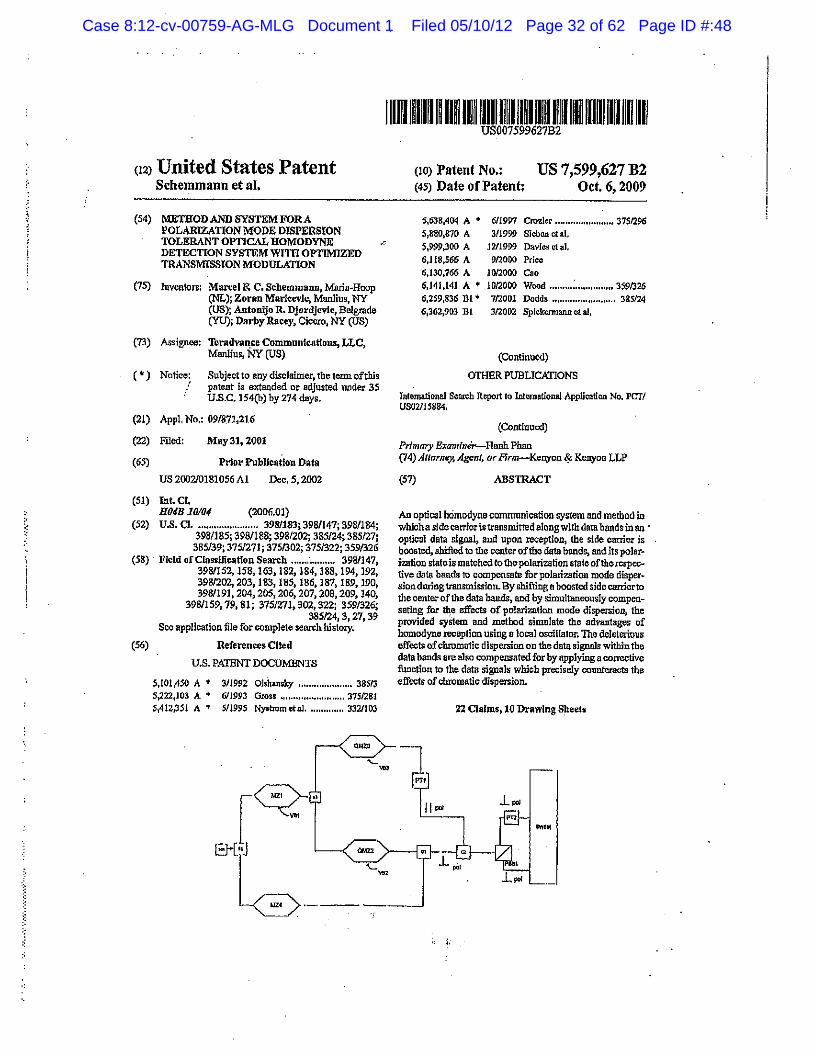
Case 8:12-cv-00759-AG-MLG Document 1 Filed 05/10/12 Page 32 of 62 Page ID #:48
,. ,, ~; :
(12) United States Patent Schemmann et al,
(54) METHOD AND SYSTEM FORA POLARIZATION MODE DISPERSION TOLERANT OPTICAL HOMODYNE DETECTION SYSTEM WITR OPTIMIZED TRANSMISSION MODULATION
(75) Inventors: Martel & C. Schemwann, Mar.ia·Hoop (NL); Zoran Mar!cevlc, Man1im1, NY (US); Antonijo R. Djordjcvl~ Belgrade (YU); Darby Racey~ Cicero, NY (US)
(73) Assignee: Tcradva~ce Communications, LLC, Manliu~ NY (US)
(') Notice: Subject to any disclaimer, the lerm. of this patent is extended or adjusted under 3S U.S.C. 154(b) by 274 days.
(21) Appl, No.: 091871,216
(22) Filed: May31, 2001
(65) Prior Pobllcotlon Data
(51)
(52)
(58)
(56)
US 2002/0181056 AI Deo, 5, 2002
ln~CI,
H04B 10/04 (2006.01) u.s. CJ, ....................... 398/183; 398/147; 398/184;
3981185; 398/188; 398/202; 385/24; 385/27; 385/39; 375/271; 375/302; 375/322; 3591326
Field ofCiussifieation Search ....•. : .......... 3981147, 3981152,158,163,182,184,188,194, 192, 39812~ 203,183,185,186,187,189,190, 398/191, 204. 205, 206. 207, 208,209,140,
398/159, 79, 81; 3751271,302, 322; 3591326; 385124,3, 27,39
See application file for complete sean:h history.
References Cited
U.S, PATENT DOCUMENTS
5,101,450 A • :311992 Olshansky ..................... 38513 5,222,103 A • 611993 G:oss ......................... 3751281 5,412,351 A " S/1995 Nyatrometal .............. 332/103
11om 111111111 m111111 1111111111~
-~
(IO) Patent No.; US 7,599,627 B2 Oct. 6, 2009 (45) Date of Patent;
5,638,404 A • 6/19P1 Crozier ....................... 3751:296 5,880,870 A 3/!999 SiebCll et al,
5,999,300 A 1211999 Davies et al. 6,118,566 A 9/lOOO Price 6,130,766 A 1011000 Cao 6,J41,141 A • J0/2000 Wood ......... : ......... ,,.,., 3591326 6,259,83G IH * 7tl001 Dodds ........................ , 385/24 613621903 Bl 3nOD2 Spickcmtann et al,
(Continued)
OTHER PUBLICATIONS
lntemational Scnrch Report to lntoro.!ltional Application No. PCT/ USIJ2115884,
(Continu<Xl)
Primary Examfnii"-Hnoh Phan (74} AttCJmey. Agcn/1 or .Firm-Kenyon~ Kell)'"Oil LLP
(57) ABSTRACT
An optical bOmodyne communicatioD system md method iD which a side carrier istrarulmitted along with data bands in an · opticu1 data signal, and upon :reception, the side carrier is boosted, shifted to the center of the data bands, and its polar~ j2ation state is matched to thepolariza.tion state ofthcrcspecw tive data bands to J;lompensate for polarization mode disper~ siondnriogtransmbsioiL By shifting a boosted side carrier to the center of the data bands, and by &imultaneou~ly compensating for ~e effects of polarization mode dispersion, the provided syStem and method simulate the advantages: of homodyne reception using a local oscillator. 'The deleterious effects of chromatic dispersion on the data signo1s within the data bands are abo compensated for by applying a corrective function to the data signals which precisely counteracts the effects of chromatic dispersjon.
22 Oafm51 l0 Drawing S~eets
..

Case 8:12-cv-00759-AG-MLG Document 1 Filed 05/10/12 Page 33 of 62 Page ID #:49
·i ·;
'
US 7,599,627 B2 Page2
U.S. PATENTDQGUMBNrS
6,404,535 Bl 6,459,519 Bl "' (i,4S9,S21 Bl + 6~08$68 Dl' 6,865,348 B2 • 7 1224,906 B2 •
· 200110050962 At• 200210109883 Al"
612002 l.olght Hl/2002 Sxsai ctal ................... 398/J83 10/2002 Ba};:l:eretnl, .............. , 3591239 812003 MurakanU etal ........... 3751261-~ :J/2005 Miyamoto eta! ........... 398/JBJ S/2001 Choetal .................... 398/183
1212001 Adachi et al. 8/2002 Schemmanu et aJ.
OTilBR PUBLICATIONS
. Govlnd P.Agmwal, "Fiber .optic:: Communtcatlnn Sy.stcm~J", Sooond Edition, John Wiley & Sons, Inc, 1997, Section 6.1.3 Heterodyne Detection, p. 242.
GovindP.Agmwal, "Fiber..OptlcCammunicatlonSystems''. Second Editioo,JohnWiley&Sons,Inc. 1997,Section 6.5.1 Ph.a:ieNolsv,p. 261. Oov1nd P. Agrawal, "Fiber-Optic CommUJI.ic:ation Sy!rtems" Second Edition, John Wiley & Sons, Inc, !997, Section 7.3.2 NonliDcar Cioutalk, Cross·Phase Modulation, p. 326. Govind P. Agrawal, ''Fiber-Op!it:: Comm.mication Systems" • Second Edition, John Wiley & Sons, Inc. 1997, Section 6.1.'2 Homodyne Dctectl.on, p. 241. Govlnd P.Agrawal, "Nonlinear Fiber Optics", Sect~nd Edition, Aca· demic Press, 1989, Section 9.4.1 Frequency-Sclectlve Brillouln Amp1ification, pp. 3.94-396. Steve Yao, .. Combat Polarization Impalrmentswith Dynamic Pola:r-1-zatlon Controllers", General Pbotonic! Corp. ~000, www . geJJernlpbotuni.;s,c;om.
*cited by examiner

Case 8:12-cv-00759-AG-MLG Document 1 Filed 05/10/12 Page 34 of 62 Page ID #:50
U.S. Patent Oct. 6,2009 Sbeetl oflO
0 c.
-l
US 7,599,627 B2
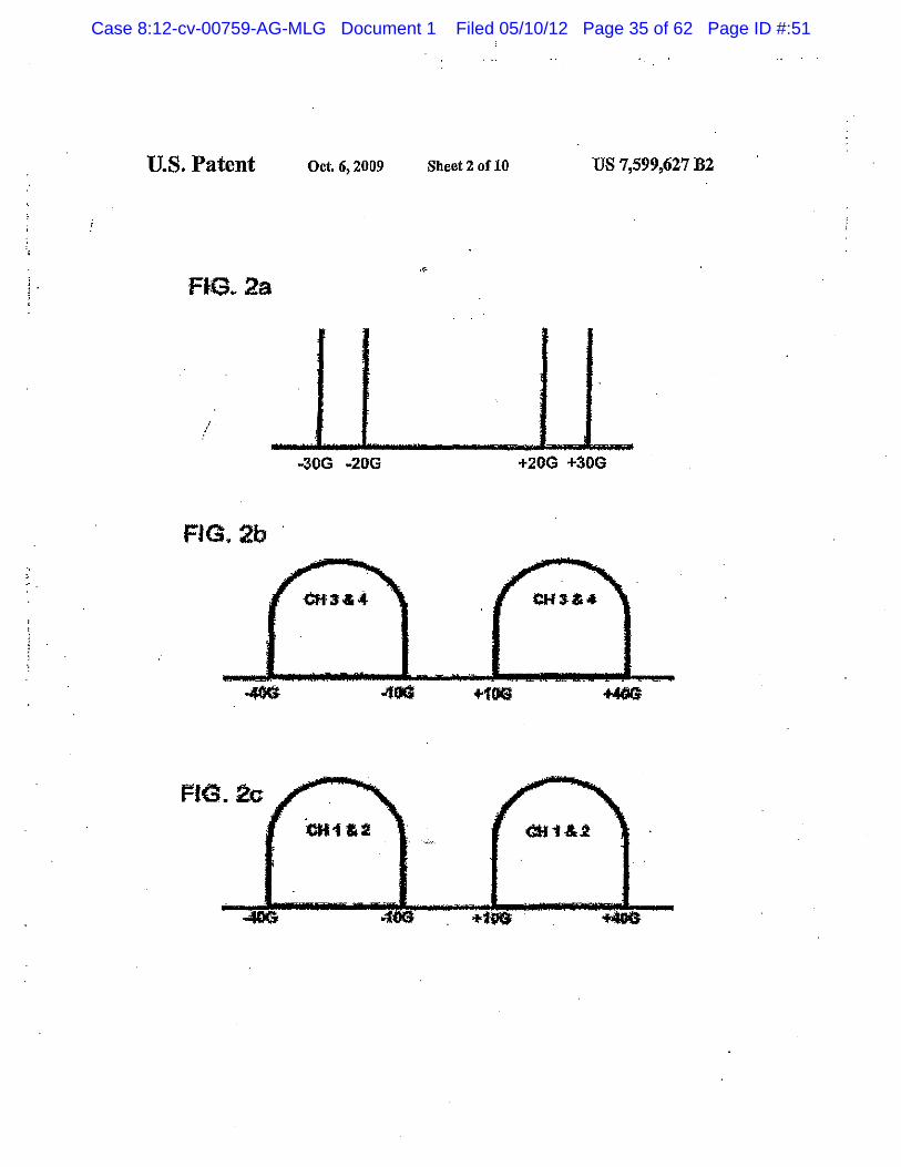
Case 8:12-cv-00759-AG-MLG Document 1 Filed 05/10/12 Page 35 of 62 Page ID #:51
U.S. Patent Oct. 6, 2009 Sheet2 oflO US 7,599,627 B2
FJG~ 2a
/
-30G -20G +20G +30G
FIG. 2b
+100
FIG. 2c CH1 &:2
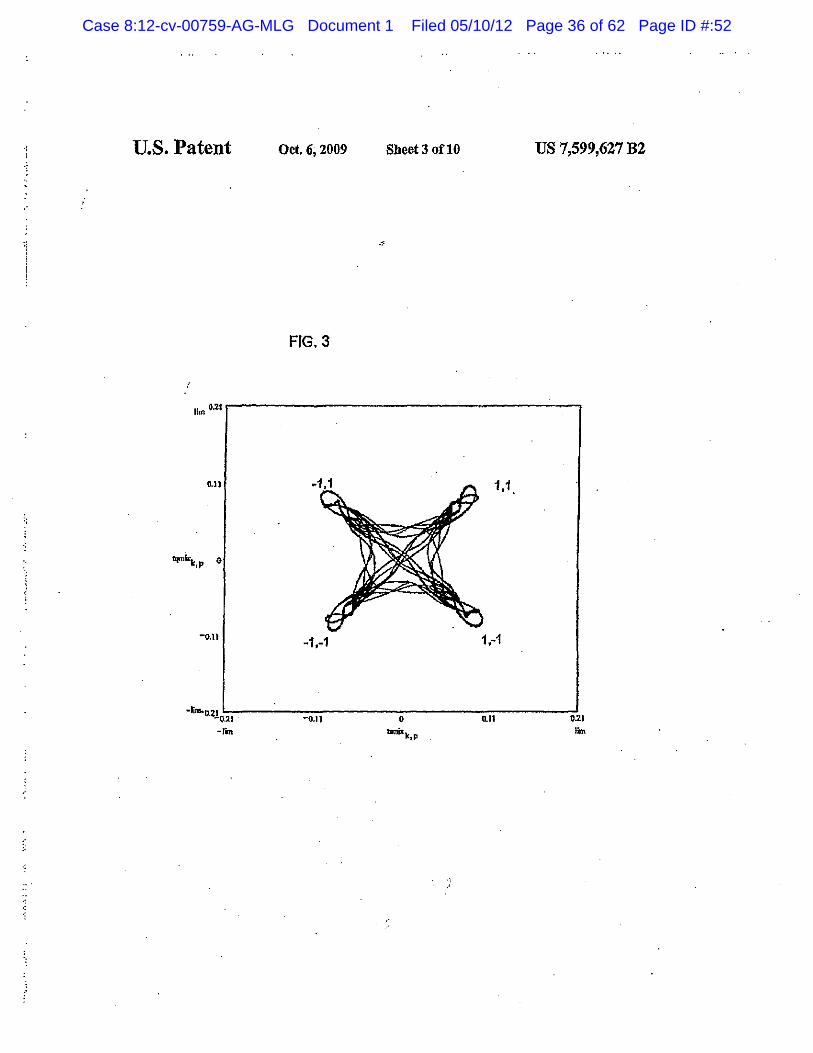
Case 8:12-cv-00759-AG-MLG Document 1 Filed 05/10/12 Page 36 of 62 Page ID #:52
U.S. Patent Oct. 6, 2009 Sheet 3 oflO US 7,599,627 B2
FIG. 3
~021r------------------------------------------,
0.11 1,1
fqrnl'li:,p 0
-o.n -1.-1
·lim.o.z!o.l:,,::-, -------_-:•""·":---------.,.,-------._-,,::-, -----:0:-1.21
-lira tlmiJ; )c, p lim
Case 8:12-cv-00759-AG-MLG Document 1 Filed 05/10/12 Page 37 of 62 Page ID #:53
·~ 'i \
::
U.S. Patent
FIG. 4a
FIG. 4b ·
FIG. 4c
Oct 6,2009 Sheet4 oflO
-10G DG +10G
CH1&2J., CH~&4 Jl
.L,Il sc
US 7,599,627 B2
CH3&4
+40G
CH1&2J. CH3&41J
·1 OG OG +100 +40G
CH1&2 2DGb/s
..Lsc
CH3&4 20Gbls
·10G OG ot-10G +40G

Case 8:12-cv-00759-A
G-M
LG D
ocument 1 F
iled 05/10/12 Page 38 of 62 P
age ID #:54
............ _ .... ;..-._ .. , .. -. ·. · ... ...-.···-. ·--·-··-···-· .. ·--.·~.
EDFA6
FIG.S I 'I . ! '
. --~---- .... ·.·-··.·:_ .• · .... "'-"•
tla1 lp/1 I I II "' ---- Tc;
Q.
OWDM31-:-f:l~ 50 Grtz . POl 8T3 ~~·
~. 0
"' 8 ·~ " "'
ml CHz : PO oil ST-4 0WOM4~
I i " I! '8
!:::1 ~ "'l:i II' :;-a.
0 " ,... !"
"' 0 0
""
IZ> =' !l Ul 0 ..... .... 0
~ ~ ~ ~
~ ~
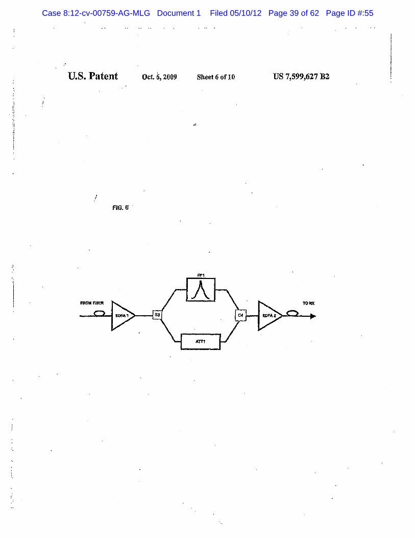
Case 8:12-cv-00759-AG-MLG Document 1 Filed 05/10/12 Page 39 of 62 Page ID #:55
U.S. Patent
' ' FIG.6
Oct. ii, 2009 Sheet 6 oflO US 7,599,627 B2
FP1
A TOIIlC
ATT1
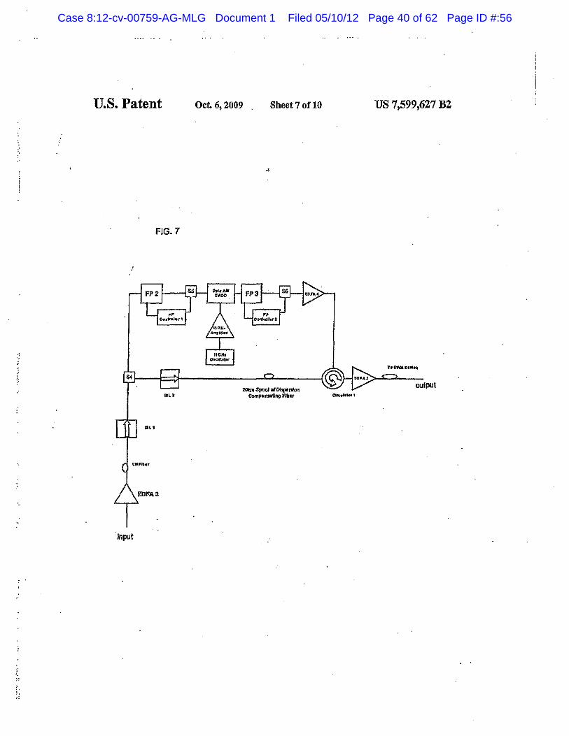
Case 8:12-cv-00759-AG-MLG Document 1 Filed 05/10/12 Page 40 of 62 Page ID #:56
U.S. Patent
FIG. 7
Input
Oct 6,2009 Sheet7 oflO
··~
2'0tPI ~ool oi'Oi5ptftloll' Compton»ling flbtr
US 7,599,627 B2
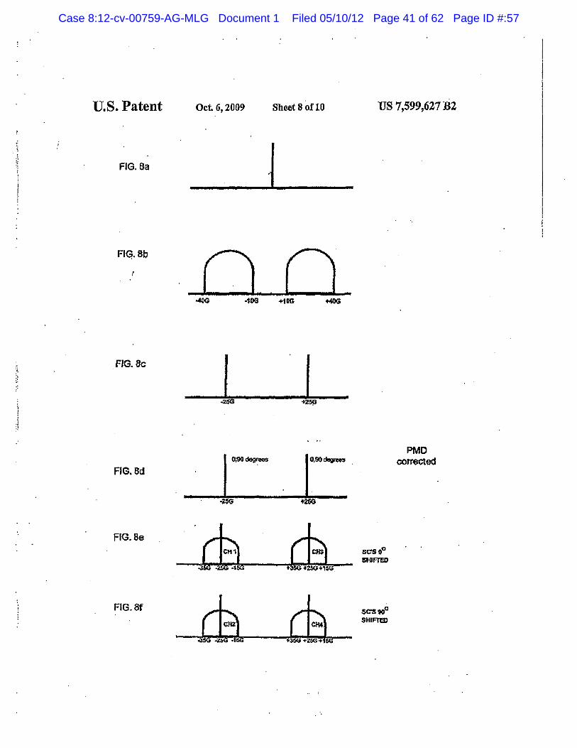
Case 8:12-cv-00759-AG-MLG Document 1 Filed 05/10/12 Page 41 of 62 Page ID #:57
U.S. Patent Oct. 6, 2009 Sheet 8 oflO US 7,599,627 B2
FIG. 6a
Fl~.8b 00 FIG. Be I I _,.. ..
\ +2~
! .; ::
,~- r- PMD corrected
FIG. 6d
~ +25G
FIG.8e ili ffi SC'S0° I5HIFTED
::tsa f'35G +25G+1&G
FlG.Bf ffi rli SC'S to0
SHIFTBl
s:w

Case 8:12-cv-00759-AG-MLG Document 1 Filed 05/10/12 Page 42 of 62 Page ID #:58
.,
I i : '
U.S. Patent
"' ci u::
.
~
"' 0 0
Oct, 6, 2009
~1
0~ -o• ,; -.sf£ i~'O dll ~,
~ z (ij
1\
0 - f--1/)
~-I -a. .5
Sheet9of10 US 7,599,627 B2
~
" 0
I 0
~
"' ::;: 0
r-
N
"' _, (/) z 0 Ci) ()
/\ Y\
~
f-'- -<IJ
.. J 0. 05
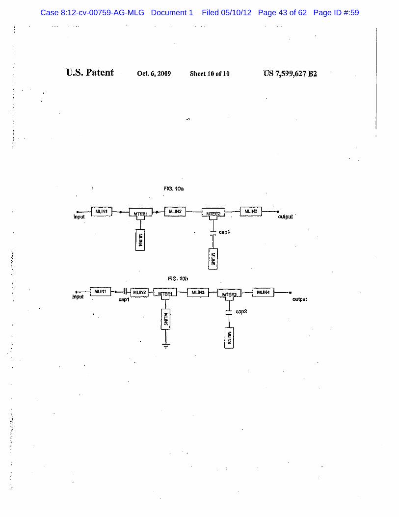
Case 8:12-cv-00759-AG-MLG Document 1 Filed 05/10/12 Page 43 of 62 Page ID #:59
U.S. Patent Oct. 6, 2009 Sheet 10 oflO US 7,599,627 B2
.. ;:.
FIG.10a
r .j I FIG.10b l ' MLIN4
output
.,..
~~
Case 8:12-cv-00759-AG-MLG Document 1 Filed 05/10/12 Page 44 of 62 Page ID #:60
".i ·I .,
:;
US 7,599,627 B2 1
METHOD AND SYSTEM FORA POLARIZATION MODE DISPERSION TOLERANT OPTICAL HOMODYNE
DETECTION SYSTEM WITH OPTIMIZE!) TRANSMISSION MODULATION
CROSS-REFERENCES TO RELATED APPLICATIONS
This application is related to copending and commonly assigned U.S. patent application Se~:. No. 09n481 7SO, filed in tho United States Patent and Trademark office on Dec. 26, 2000, entitled "Method1 System and Apparatus for OpticaUy Tmnsferri.ng Information ...
FIELD OF THE INVEN!10N
2 method in wbich a reduced amplitude side c:anieris ttnnsmit· ted along wllb data bOIJds in an optical data signal, and Upon .reception,. the side carrier is boosted, shifted to the· center of the data bands, and its polwizution state is matched to the
s polarization stale of the respectiye data bands to compeDSate for polarization mode dispersion during transmiasion, Thls scheme achieves the signal.to-noise benefits of homodyne reception without inc wring theconverrtiOnal restrictioos and complications ofhomodyne reception such as .requiring the
10 phase o:f' a signal from a local oscillator to be locked to the phase of the optical signal ..
According to one embodiment, the present invention provides a method of optiCHl communication that begins with providing a quadrature modulated optical data including two
15 data bands separated in frequency, each datn band having in-phase and quadmture components. The power of the
The present invention relates to optical datu communica- quadrature modulated optical data signal is limited in order to tion, and in J!arlioular, relates to a method nnd optical data limit ~onwlin~ effects ~y reducing t~ po~er of the optical communietl'tiOn system tbatimproves sigoalwfD..noiseratio of data Sllplal dunng ~sttional ~tates tn wht~ data symbols optical data signals, cou.nteractspolarizationmodedispersion 20 ~Olltted in the optical data stgnal change m value, ~din nud improves robustness to fiber nonlinearitl particular by reducing the powert? zero such that transmttted
es. power decreases to zero st approxtmatelythe mld point oftbe BACKGROUND D"'FORMATION transitional states, The Optlcal data signal is combined with a
slde carrler at a single frequency between the two data bands Currently, optical datu communication systems are being 2S of the optical data signal and thtm transmitted across optical
upgrnded from c 10 Gb/s data transmission rate up to a 40 fiber to a receiver. Gbfs tmnsmission rate. However, data transmission at 40 At tbe receiver, the side carrier is separated from the twa Gb/.<1 (or higher) presents extensivedesigo.chalienges 'because data bands of the combined optical da1a signal and increased the effects ofpolarizationmode dispersion(PMD), cluomatic in amplitude relative to the data. The side carrlen; are then dispersion ~nd fiber non~ linear effects such as crosswphase 30 shifted to 1hemiddleofeachofthe respective two data hoods. modulation become more dominant at the Wgher transm:is~ Since the relationship between the polarization state of the sion rates. In particular, t:lle limit of tolerable Pol~rization side carriers and tho polarlzatlan state of the data bands does mode dispersion, urmaJly defined as 14% offue data bit dura- not stay constant during transmission over optical fiber1 the tion, is only 3.5 ps at a 40 Gb/s transmission rate. A 3.5 ps polarization state of the &bitted tcide carriers is adjusted to polarizationmodedlspcrsion translates to no attainable reaCh· 3S match the polarization state of the data bauds at which they of saveral hundred kilometers over single mode fiber which ~ ce.nlen:d. bas a typical fiber PMD afO.l pslkm112.. The present invention fut1her provides a method of comw
Current optical communications systems, such as tho PMD P:CS?1ingfor the ~1fects of chromatic di~persio.o. during trans~ compensation arrangement described jn U.S, Pat. No. 6,130, mtSSIO:Q over op1tcal fiber by separatmg the in-phase and 766 10 Gao, generally attempt to compensste for PMD by 40 qua~ture components o~the two da~ bands prior to aplow splitting received optical signals lnto x andy mode campo- olectric coavenrlon, and, after optoelectrlc oonversion1 comw nents having ortbogonaJ polnrizntian, t~nd then t~djusting the pen sating for chromatic dispersion by applying a corrective delay on one of the orthogonal components to align the function to each of the lnwphase and quadrature components modes. This anangumentrequires significant signal process- of the data band~ the canective function precisely COlmterw ing and differen.tial delays to cover lhe runge of :freqUencies 45 acting1he effectsafcbromaticdispersiono.n theln-phaseand carrying data. quadrature components.
Nonlinearities induced duringoptical transmission are also • The present inven~on also prov!des a method of providing amplified at higher data rates, While it is necessary for acCu- info~tion concenung a transmassian device by providing rate"dete~on that optical data signals be at least 20 dB above . anopttcal data signal having data bands uncle sidccar.rierwith background noiso, if the data signals are transmitted with loa so the side canier modulated to cauy an identificHtion code, the much power
1 nonlinearities can play a greater role in distort~ ident~<;ation Code including infob:natioc. canceming the
ing the signal. ln addition, in eoberent systeDl8 typical !ret- !Jan~itter, According to m em~odiment of. the present . erodyne optical reception .systems suffer an inherent 3 dB mvcntion, the information cancenuog a traDS.Illltler embed-penalty with respect to homodyne systems and jotroduce ~edinthe.si~carrie;includesparametersusedinthecorrecw phase noise through use of a local oscillator, and tlwreby add ss ttye fu~ction to pree1sely counteract the effects of chromatic a further level of complexity andco.ostmints to optical system d1Spers1an. design. An optical data signal tra.nsmitter is provided for general-
What is therefore needed is a cost-efi"ective method and ing1he quadrnture modulated optical data signal including at system that compensates for PMD, optimizes SNR per.l'or- Jeastoneside~arrier. Thetransmitterincludesa MachwZender mance and minhnizes phase noi!ie and nonlinearilie~ associw 60 modulatorwhichgenem.tcs an optical cmrler sigoalby modu-aied with tmnsmissian over .fiber at high data transmission lating a t'Bir of side cmrien onto an input optical signal. The rates. optical carrier signal is modulllted by m: Jenst two phase
modulators which modulate a pair of data signal!!, in quodronlre, onlo the optical caniersignal, outputt.iug an.oplical data
6S signal including at least two data bands. By spreading the data SUMMARY OF THE INVENTION
The present invention meets the above objectives by prow bands onto the pair of sido carriersJ the amplitude of the viding an optical homodyne communication system and optical data signal 1s reduced to zero during transitions

Case 8:12-cv-00759-AG-MLG Document 1 Filed 05/10/12 Page 45 of 62 Page ID #:61
i I .,
.,
·! ,_
US 7,599,627 B2 3 4
between data symbols. The transmitter also includes a second Mach~Zender modulatorwhichimprints a low·frequencyTX ID (transmitter identification code) sidecrurieronto the input optical signal. The TX ID signal side carrier then combined with theoptica1 data signal for transmission. The transmitted l identification code. includes information concemlng the""' transmitter, such as its location, 'from which the distance between the tmns.mitter and a receiver may be deduced.
PIG. 8c shows the spectrum of an optical canier signal at the ou1put0fthc PBS3 ofFJG. 5accordlng to an embodiment of the present invention.
FJO. 8d shows the spectrum ofnn optical carrier signal at the output of1he SSl ofFJG. 5 acCording to an embodim~nt ofthe present invention.
FlO. 8e shows the spectrum of an optical carrier slgnal at the output of the C5 ofFIG. 5 acconiing to an embodiment of the present Invention. Theprerent invention further provides a receiv& tbr imple
menting homodyne reception, 'lbe receiver includes a side carrier boosting module for increasing the amplitude of 1he side ca~rierrelative to the data bands jn the optical data signal, The receiver further jncludes a side canier shifting module C9Upled to the s:lde carrier boosting module which shills the side carrier into two shifted carriers. Each of the shifted caniers is shifted to the center of one of the data bands. In addition, means for compensating polarization mode disper· sian that are coUpled to the side canier shifting module match the polarizati.6n states of the shifted carriers to theda1a bands by adjustingCither tbe polarization stateoftheshifted caniers or the polarization stata ofthe data bands. After optoelectric conversion of the optical dala signal, the receiver employs a chromatic dispersion correction stage tlwt includes circuits that apply transfer functions to the in~phase and quachature
10 FIG. Sf showS the spectrum of nn opticni conier signal at the output of the C6 ofFJG. 5 according to nn embodiment of the present invention. · ·
F1G. 9 is a block dlagram of a chromatic dispersion com· pensation circuit accor&ng to an embodiment of the present
lS invention. FlG.lOa is a biockdiagmm ofamicrostrlp implementation
ofn circuit that applies a COS tlanS'fer fimction 1o an input signnlt~ccording to nn embodiment of the present invention,
PlG.l Oh i~a block diagram of a microstrip implementation zo of a circuit that applies a SJN transfer function to an input
signal according to on embodiment of the present invention.
DBTAlLBD DESCRIPTION
detected data channels 2.S ], Transmission
BRJEF DESCRIPTION OF TilE DRAWINGS Inaccordancewith the present invention, at a transmitter, a pair of side caaicrn is modulated onto each side of a monow
FIG. 1 is a block diogmm of a trfUI.Iim.itter nccordlng to an chromatic optical ~nier si~, ;arhk:h is then ~lit into two bodlm t ofth t invention JO channels, Bach opbcal earner stgnal chiiWlellS modulated
em en e presen · . · • . with two 10 Gb/s data signals in an orthogonal phase reln~ FIG. 2a shows the spectrum of~ opt teal earner ~lgnal at tionship lo one another. The data signals am spread on1o the
the output o.fMZl: ofFlG.l according 1o an embodiment of "two :side.cao:iersin each channel, and in effec~ are spread out the present mvenhon. • . by fifty 'p<::rCent in the frequency domain. Thl:s spreading is
FlG. 2b shows the spectrum of an optical ?at~ Signal at the 35 equiValent to multiplication by a sine wave at half the data output?fQMZ3ofFJG:lafterdatnmOdula~onm~uadrature ra1e, and results ill each data symbol returning to zero acconling to an emboth.llleJll of the present mvenhoJJ, between tmnsilions
1 referred to as quadmture-rcturn-to-zero
FIG. 2cs00ws the spectrum o~an optical data signal at Uio (QRZ). Using QRZ, the"power of tbe optical data signal is output ofQMZ2 ofFIG, 1 according to an embodiment of the wade independent ofthe data pattem: The polarization of one present invention. 40 of the optiC"al data signal channels is then shifted1 and one of
FJG. 3 shows a lOG symbol per :second Quadratare Return the channels is combined with a channel of the original mono~ to Zero (QRZ) constellation dlagtam of the output JTom chromatic carrier thllt has been modulated with a tran:smis~ QMZZ and QMZ3. · sian idenfitication carrier ofJess than 100kHz.
FIG. 4o shows tho speclrum of an optical data bignal at tho The two optical data ~Sila1 bands, whlch each carry a 20 output of Cl of FlG. 1 according to an embodiment of the 45 Gbls data stream, are combined and eilber multiplexed with present invention, adjacent c.bannels at similar frequency and orthogonal polar-
PIG. 4b sbowx the spectrum ofnn optical data signal at the ization or one of the two c~els is shifted in ~larizati~ to Output of C2 of FIG. 1 according to an embodiment of the match the other channel. In e1tber case~ the optical data stg· present invention. .naJ:s. Wl' ~ultiplexed according to a Dense_ Wave Divjsion
FIG. 4c shows the spectrum of an optical data signal m the so Mulitplexmg (DW_D~ sc~e and transmJUed along long output ofthe DWDM ofFJG-.1 according to an embodiment haul fiber to fl dcsunatlon re~~· , . . of the present invention. FIO.llDus~tes a~embod~entofa tc~smitteraccording
FIG. 5 i:s a block diagram of a n:ceiver according to an to. ~e pre&ent mv~UODI which may be ~pfementecl on. a bodlm nt fth 1 iDventio.n Llthium-Niobatcchip, forcxampJe.Anoptical signalgeoera.
em ~ 0 e p~esen ' • • ss 10r SGl, which may be a laser, generates a monochromatic, ~G. 6JS a_bJockdmgramof~firstembodlDlc:ut.ofthe. side polarized optical carrier at a reference frequency which for
earner bo?:stlng mod~Je according 1o the presen! mv~tion. purposes of the following discussion is designated as the . FIG.~ 1s a bJo~k dtagram of a se:oJJd embodiment .of the origill (0 GHz) in terms of relative frequency. The optical
s1de carr:er boostmg module ~ccording to .the ~resent mv~- signal is !hereafter split into two channels:, an upper channel ~on which employs the Stimulated Brilloum Scattenng 60 going to Mach-Zemlcr modulator MZ1 and a lower cbannel (SBS) effect. being transmitted to MacbwZender modnlntor MZ4. Tbediv:iw
PlG. Sa shows the spectrum of an optical carrier signal at sionoflightintenslty between tbt't?lo chwmels canbell!leven tbe output of the FP4 ofFlG. 5 according to an embodiment with fuelowerchannel receiving, forexample,just] Open::ent oftheprcscntinvention. of the light intensity generated by SGl. At nanow-band
FlG. 8b shows tht) 1;peclrtlm of an optical earrier signal at 65 modulator MZ-4, the lower ~hanne1 of the opti~al signal is the output of the S7 ofFIG. Saccordingto an embodiment of modula'ted with a "Transmitter Iden1ification'' {TX ID) tone the present invention. i.o. the freqUency .range of 10KHz to 100KHz aboYe the
Case 8:12-cv-00759-AG-MLG Document 1 Filed 05/10/12 Page 46 of 62 Page ID #:62
US 7,599,627 B2 5 6
reference frequency. At modulator MZl, two sets of side para:l1elpoJarization. ThereferencecanieratapprolrimatelyO carriers at+/-20 GBz and +1-30 GHzaremodulated onto tho GHz from MZ4 is in perpendicular polarization. optical signa], The spectrum for the modnluted sigoaJ, Accordlngtotheillustratedembodim~rot, the output signal denoted an optical-carrier signal, is shown jn FIG. 2a. As 'from C2 is input to a polruiwtion beam splitter PBSl which shownln the figure, the resulting spectrum output from MZl s splits the signal into perpendicular and parallel polarized shows four peaks, two below the reference :frequency at -30 components, thereby sepaiating the data olmnnels 1 and 2 GHz and -20 GI-Jz relative to the reference frequency, and'' from channels 3 and 4. The perpendicular component (con" two above the reference frequency at +20 GHzand +30 GHz. taining data channels l8Dd 2 as weD as the central reference
The output of modulator MZl.is further split into an upper :frequency) is transmitted along lowerpath 102 to a first chan~ .cbalUlel which is transmitted to quadrature data modulator 10 nel ofadcnsewnvedlvision multiplexer DWDM, thepara1lel QMZ3 and a· lower channel whichistronsmitted to quadrature component (containing data chrumels 3 and 4) is input to a data modulator QMZ2. Data modulator QMZ2 imprints two polarlzution transformer Pn, which rotates the polarization indlviduallO Ob/s data streams in quadrature (in orthogonal ofthepamUel component back into a perpendicular state, The phase rela6onsbip) CH.l and CH.2 onto each of the palls of output from PT2 is then input to a second DWDM channel. slde carriers above nnd below the reference frequency. Simi~ 15 Each DWDM channel nets as a band pass filter and passe' Jarly, data modulator QMZ3 imprints individuall 0 Obis data only frequencies that :full within a 50 GHzband.Assnmingfor streams CH.3 and CH.4 onto each ofthepairs ofside can:iers illustrative purposes that DWOM channell paJJSes frequen-ln lhe optical Carrier signal. Respective bias control clec- cies :from -50 GHz to 0 OHz relative to the reference fro-trades VB2 f1b:d VB3 assist in keeping the data streams in queocy, and DWDM ohannel2 passes ji-cquencies from 0 til quadrature. Spectra oftheoutpotsfrom QMZ3 and QMZ2 are 20 +:50 GHz, datn channels 1 and 2 are passed only in the data shown in FIG. 2b and FlO. 2c respectively. As can be disM band from --40 GHz to -10 GHz and while data channels:\
, cerncd inFlG. Zband FIG. 2c, the output spectrafromQMZ3 and 4 are passed only :in !he data band from+ 10 GHz to +40 and QMZ2 show two data bands, one extending from -40 G& The DWDMmultipJexes eachofthe _passed bands onto GHzto-lOGHzandanotherextendingfrom+10GH:r.to+40 a long haul fiber(not shown), The output spectrum from -50 GHz relative to the reference frequency. 2S GHzto+50GHzoutputfromtbe DWDMis shown in FIG. 4c.
By imprinting two 10 Gbls data streams in quadrature, in The' adj,qccnf. DWDM channels each pass 20 Obis of data, effect, 20 Gbls of data are modulated onto each pair of slde combining for a total of 40 Gb/s. carriers (-30,-20 GHz and +20, +30 GHz> respectively) and ln an alternative embodiment, a polari:mtion multiplexing each 20 Gb/s dam hand covers 30 GHz in the :frequency schememaybDused, making it unnecessary to separate data domain. Byprovidingtwa side carriers, with one side carrier 3D channels 1 and 2 from data cbannels 3 and 4. in thepnlrn clockrateawayfrom theother(i.e.,30GHzbeing As described in related and commonly owned application a clock «Way fram 20 qHz), the data bits in both I and Q Ser. No. 09n82,354 hereby incorpomted for .reference the format are multiplied in the time domain by aS G& sinusoid pairs of data channels can occupy the same data band iffueir which crosses zero every 100 p.s. Thus. the total data signal polarization states remain orthogonal and thus do not inter~ ahwys crosses through zero in between any pair of symbols 3S fere with each other. Jn this implemen'tation, the polarization (nny pairofl,Q data),referredtoas quadrature-retum-to..zero beam splitter PBSl is .not needed and the output from C2 can (QRZ) modulation: · be sent directly to one of the DWDM input clumnels.
FIG. 3 illustrates the key property of the QRZ foriQat, · showjcg that the trajectOiy between two successive symbols IT. Reception , . always leads through the I-Q origin. Eacb corner of the figure 40 Jn ~ccordance .w'th the present ~vc:ntion, ~ homodY?" represents a pair of 1, Q data symbols (e.g., I=l,Q=-1 or reception system 1s e~ployed to recewe the op.tlcnl dam SJg-I=-1, Q=l).Asshown, to getfromadjacentcomerpointsi=l, ~ gen~tedlls descnbed above. Upon recepti?n, tho trans-Q-1 (upper right comer) to l=l Q=-1 (lower right corner) Dllttcd s1de carrier nt the reference frequency 1S boosted to the optical data signal must tra~eJ through tho origin (0,0). i~crease the signal-to-noi11e ratio (SNR~ of the o~Ucal ~Ia Dnrlng each tnljectocy thn>ogh the origin, the power oftbe 45 wgnahmd to ~ompensate fbr~he Bttenua~onof~st~e earner signal whichisproporliontothesquareof:ltsamplitude goes in the trans.rmtter. Tb boosting of the Side camer mcreates to ze;,,
1 the SNR because oft:hB impleme.otation ofhomodyne recap-
Returning to FIG. 11
the output from modulata:r QMZS is tion h1 which owmll detected signal,power is.increased in input to a polarization transfonner PTI1 which shifts lhe proporti~tothe?awerofthelocaloseillator~orm~epres~t polarization of the optical data siSJl;lll output from QMZ3 90 so case(as will ~e di~aussedbelow~ the ~smJttedst.de earner. degrees, The polarlzatiOJl of the signal ootput from PT1 ls Once tho- aropbtude of the sJde camer power lS boosted arbitrarily iUustrated by parallel lines as parallel polarization rel,ative to fue fransmi~ed data ~aads, t?e side carrier is as oppo&ed t6 a perpendicular polarization of the original s~ftcd by +1-25 GHz mto two nde camers thnt are each optical signal. Furthenno~ the output optical data signal sbiftcd to 1he center of one of the two data bands to further from modulator QMZZ is combined at combiner ct. with the ss implcmenthomodync reception. TX lD pilot signal :from MZ4. The output from Cl is shown After 1he shiffing of the sideearriers, tbe two side carriers in FlG. 4a.As noted above, the intensity of the 1'X ID signal are separated and then modified by polarization controllers is reduced in comparison with tbe optical data signal from which match the time-varying polarization state of each the QMZ2. It is also noted that the polarization of tho output· sideauriemtothedifferenttime-varyingpolarizationstateof signal from Clls shown as pespenclicular, since the polariza~ 60 the respective data bauds, thus overcoming the effects of tion oftheoutputfrom Cl remainsuncbaoged ftom theorigi- polarization mode dispersion by controlling the polarization naJ polarization. Thereafter, the output signal from PTl is at only a single frequency. combined with theoutputrrignal frumcombinerCl atC2. The According to an embodiment of the present invention, a spectrum of the output signal oul ofC2 is shown in FIG. 4b. chromatic dispemon compensation stage is used to counter As can bodUicemed, tbeSJiectmm includes data channel' 11 '2, 65 the effects of dispernion during transmission over long haul 3 and 4 jn both lower and upper data bands, Channels 1 and 2 fiber, Since the: effects of dispersion can be modeled as a are in pcJPendic:ular polarization an.d channels 3 and 4 aro in transfe~ function that is applied to thel and Q data signals, the

Case 8:12-cv-00759-AG-MLG Document 1 Filed 05/10/12 Page 47 of 62 Page ID #:63
~: :: i:
I I
US 7,599,627 B2 7 8
chromatic dispersion compensation stage applies a compen¥ em:efrequencrand two Bide frequencit:S located 11 GHzboth sating correction function that Wfectively coonteracts 1he above D.Dd belDW the reference frequency, This output signal transferfunction1 renderlngthe!andQdmasigo.als:iototheir is then transmltted to ·another resonator FP31 wbicb is original non-dispersed slaW. adjusted by FP controller 2 to center QD (and pass) only tho
FIG. 5 illustmteS an embodimen1 of a bomodyne nx=eiver s side frequency 11 GHz above the reference side carrier frt'l-accotding to the present invention. An optical data slgnal is quency. The resulting signal, carrying substantially a single received first by a side carrier boosting module 200 farwhich"' frequency at the reference frequency + 11 GHz1 is amplified in the present invention provides two exemplary embodiments. optical amplifier BDFA4 and then input to circulatorCIRC 1. In a first embodiment of 1he side cattier boosting module, The circulator passes idgnals in a counter-<:1ockwise direc-shown in F1G. 6, the optical. data signal is first input to an 10 tion. More specifically, CIRC 1 passes the output from optical amplifier EDFA11 which may be, for example, an EDFA4Iuftwardsinacounter-clockwiserotatiantowards1be erbium-doped fiber amplifl.or (EDFA). It is notod thnt all outputofopticalisolator1SL2.ltisnotcd thatfucside canier further optical amplifiers used in the implementations boosting scheme is also intended bDused in conjunction with described below may be implemented as erbium-doped fiber n dense wave <livlsion multiplexing scheme. Thus, the side amplifiem, The opticnl amplifier EDFAl amplifies the entire 15 carrier boosting module can simulmneously process and spectrum of the received signal by, for example, appro xi- boost apJumlity of side carriers tr'])aced in frequtmey accord~ roately 15-18 dS. Tha I:Dllplified !ligna I ouiput from BOFA1 is ing to ITU channel spaclng, spli1 ·at S3 between an upper branch thaf is coupled to a Sjmultaneously,theopticalsignalinthelowerbranchfrom Fabry-Perot resonator FPl and a lower branch that is coupled splitter S4 is tranSJl.'titted through isolator ISL l and then to ao attenuaior A1TI. · 2.0 meets with -the optical signal from the upper b.mnch output
The Fabry Perot resonator FPI :t\lnctlons as a high-Q filter from the circulator CIRC 1. This colllsion of the two optical 1batnearlycomp!etely:filtersoutallfrequenciescxceptsfora signals travellng 1n opposite directio.ns generates the SBS series of :frequencies that are separated by, for example, 100 non#lineareffect.Accordingto one implementation, the fiber Ghz which, according to the International Telecomnmnica- connecting isolator lSL 2 aod circulator CIR.C 1 can be dis· tion Union (ITO) grid, ls the J!.DlOunt of bandwidth allocated 25 persian compensating fiber whlcb, due to its relatively for each thannel. The resonator FPl is adjusted to pass the smaller cross-seetio~ promotes higher intensity and more side carrier at the reference :frequency and :filter our the data pronounced non-linear effects mch as SBS. When the optical bands of the optical data signal. It b: noted in this regard that data signal conialnlng the reference side carrlcrcolHd~ whh it is contemplated that the embodiments ofthe presentinven- the 11 GHzsidefrequency signal fromCIRC:t, a nsnowband tion be med in the Context of the 11U grid, and that the JO including1beside Carrierin the optical data signal is amplified 'reception approach described allows for simultaneous pro- relative to tho data bands due to the SBS efiect as explained cessing of side carriers for a plurality of lTII grid~spaced above. This modified optical data signal then reaches the cbannels. The lower branch passed to ATI'l, which contains ciroulatorCIR.C 1 from which it passes in the counter-clock~ both the data bands and the side canier is attenuated. The wise direction lo optical amplifier BDFA5, which amplifies signals output from FP:t andATI'l are combined in combiner J5 the: entire spectmm of the modified optical data signBl by C4 and then passed to a further optical amplifier BDFAZ lS..l8 dB. The output from BDPAS ls the final output of the where the combined signal :is again amplified by, forexw:ople, second embodiment of the side carrier boosting module 200. approximately 15~ 18 dB. Because the side carrler was iso-- Returning to FIG. 5, theoplical data signal output :from the Ia ted and boosted in FP1 and the data bands were attenuated side carrier boosting module 200 is input to circulator CIRC in.AT'U, the cambh1ed signal contains a side canier boosted 40 2, which in tmn transmits the signal in a counter-clockwise at least 10 dB in amplitude relative to the data bands. direction to Fabry .. Perotresonator FP4, having a free spectral
A second embodiment of the side caniei boosting module, range (FSR) ofl 00 GEz and ftnes$e on the order of 1 000. The whichadvantageo_uslymakes'DSeoftheamplitude-enhanciog resonator FP4 is also tuned to select the side cmrier at (ap-elf«t of Stimulated Brillouin Scattering (SBS), is sbown 41 proximately) the reference frequ011cy (0 GHz). FIG. 8a FIG. 7. The SBS effect cmlSes a first optical sJgno.1 having 4S shows a spectrum of the signal output from FP4, indicuting narrow frequency band around :frequ"ency X to be ampHfied 1hnt tbe dam bands have again been filtered out The data when collides with a slgnal offrequency X+>-<ll GHz travel- bands that are filtered out at FP4 are resent back toward lnginthe opposite direction. Referring to FIG. 7, tberecelved circulator CIRC 2, where they are redirected in a cmmter~ signaljs inputtooptical amplifietEDFA3 which amplifies the olockwho direction towards splitter S7. The spectrum of the entire spectrum of the input signal,. The signal output :from so output :from splitter 811 which includes the two filtered data amplifier BDFA3 is transmitted to optical isolator ISL 1, bands at-40OHz to -10 GHz and +10 GHzto +40 GHz, is which permits optical slgnal to travel only in one diremion shown in FlG. Sb. (the direction indicated by the arrow in the figur6) and pre~ lt is noted that when the optica1 data signal is transmitted vents optical signals being reflected or transmitted bac:k over Joog haul fiber between the transmitter and the receiver~ toward the amplifier EDFA3. From the optical isola toe ISL 11 55 the polarization state of the transmitted signal is scrambled, the optical data sigoaJ is split into two branches at splirterS4. with the result that the received signal has an unknown time..
A first upper branch from splitter S4 leads to Fabry Perot vm-ylng p::l'Jarization state. Since tho time-varying pol<~riza~ resonator FP21 which passes lhesidecarrier(andother modes tionstatevarieswith frequency, the side carrier is expected to in the series of frequencies) in betweon the data baDds. FP have a di.fferenttime-varyingpohui:zation state than ejtberof controllerl automatically adjusts the resonator FP2 so that it 60 the data bands because it js separated from tho contersof data correctly passes the side carrier using input from spUtter 85 bands by_ 25 <;iHz. When the output from resonator FP4 is fed and filters out the dam brulds. The output from FP2 is deliv· to the side Cnnier shifting module 210, tho sidCi\ carrier's ered to external modulator XMOD l, which also receives an orthogonal polwi7.ation states are split in polarization beam 11 GHz signal from all OHz oscillator through an 11 GHz 5plitter PBS2, and then each of the orthogoital signals are amplifier. TheexterJlBlmodulatorXMODl modulatestbe 11 65 separately inddulated by 25 GHz inXMOD2 and XM0031
GHz signal onto the side carrier. The spectrum of the output re~tively, and then joined back in PBS3, The output from from the modulator XMOD 1 thereafter contains the refer- PBS3 is illustrated in FIG. Be, which shows two side carriers

Case 8:12-cv-00759-AG-MLG Document 1 Filed 05/10/12 Page 48 of 62 Page ID #:64
.,
::
US 7,599,627 B2 9 10
at-25OHZ" and +25 GHz from the rofereo.ce frequency, RetumingonceagainfoFJG.S,Ihepolarizationcontrollers respectively. The output from PBS2 is passed on to Fnbi)'· PC 1, PC 2 ou1put polarization compensated side carrier Perot filter PPS (FSR=50 GHz, finesse>SOO) which pas~es signals to ci.rculator CIRC 3, from which they are forwarded both the 25 GHz left and right shifted side carrien1 and tosplitterSSl. T.hesplitterSSlalsoshiftstbephaseofoneof transmits them to circulator ClRC 3. Ci.rculatorCIRC 3 deljy.. 5 the output branches by 90 degrees relative to other branch. en> shifted sc•s to refieclivepolarizationcontrollero PC 1, PC., The output spectrum from SSl iS" shown in FIG, 8d. These 0 2, througb respective ndjocent 50 G&~spnced chonriels of· degree nnd 90 degree phase shiftedcaniers are recombinedln WDM demultiplexer DWDM 2. The polarlzatio.ocontrollers combiners CS and C6J respectively, with the data bands out· PC 1, PC 2 are constructed to provide cOntrol of the phase of put from splitter S7.ln-pbase (0 degree shifted) and quadra~ Ute signals reflected from the polnrization controllers back to lO ture (90 deg;ree-!ihifted) signal spectrums out of outputs of ~e demultiplexer DWDM 2. Such control m;o/ be used, fur respective combiners C5 and C6 are show .a in FlG. 8e and inStnn~e,ln order to compensate for the e.ff'ecnve fiber length PIG. 8f As can be discerned~ in each spectrumJ a side carrier between the :polarization controllers PC 1, PC 2 and the i& positioned in thci confer of a data bfUld. Each side of the demultiplexer DWDM 2. In one implementation, the polar- spectra is equivalent to a spectrum generated by a conven~ fzatlon controllet'll PC 1, PC 2lncludemirmrs nnd piezoelco- 15 tioool bomodyne system in which the loc11l oScillator fre. tric actuators to adjust the digtance the reflected signal travels:, quency is zlmtched to the center ftequency of1he data band. wbichintumconlrolsthepbaseoflh~reflectedopticalsignal. Furthermore, as in conventional homodyne reception, the
power of the central carrier frequency is boosted relative to Each P~~zati~n contro.ller. PC 1, PC 2 is used to tra?S· the data portion in order to the Improve slgoal-to-noise mtio
fern; thetJme-varymgpol~J~bon:staleofone of~etwo sJ.de 20 of the detected signal. The :side carrier that bas been sbifu:dO earners so that the p~lanzatio!l~>~tes of each s1de ca~er degrees can be used to deteot the in-phase (I) 10 Gb/s data match~ the time varymg polanzation state of the respective channels from the transmitter (channels 1 3) d th 'd data bands which arc centered at the side canier (-25 GHz carrler that has been shifted 90 degrees ca 'b ~ t d 5~~ and+25GHz). Toa~complishlhis,eacllpolarlzatio;tcontrol~ the quadralllre (90 degree shifted) 10 G~se;:ta c~a!els Jer ~C 1, PC2 obtams feedback from the pho1odiodes that 25 (channels z, 4). recmve the data bands. PC 1 recerves the feeback via bias-T • couplers BT 1 nnd BT 3, while PC 2 rel:elves feedback via Th_e combined sr.goal from ~ is sent throlJgh ~ptical bias-T couplcis BT 2 and BT 4. As will be deS"cribcd below, amplifier BJ?PA6 and. the combmed signal from C6 15 sent tbedemultiplcxersattbetopofFIG 5 DWDM3 DWDM 4 through optical amphfier EDPA1 to final 50 GHz spaced receive both the datB b!lDds 8lld th~ si'de c~trriers: filter th~ 30 ~emultiplaxers DWDM 3 nn.dDWDM 4. Ench oftbe demul-.into separate, adjacent frequency channels and then e:ffec- tiplexers. DV!DM. 3, DWDM 4 separate the data bands and tively multiply the side carr:ier and data bands togeth t Sidecam~mnnadJacentcbannclsforelectro~opticconver.sion photodiodesPDI, PD2, PD3 andPD4 (andotherphotodi~~ atphotodiodes PD 1, PD2undPD 3, PD4 ~JlCctively.ln th~s ofadjacentchnnnelsthatarenotshown)whichrespondto1he manner 10 GB/s data chmmels 1 aod 3 me separaled ~ intensity of the sjgnaJ (i.e .• the square of the amplitude). The
35 DWDM 3 and l ~ G?ls channels 2 and 4 are separated m
product signal output from thephotodiodes is delivered to the DWD~ 4, resulting m the output of fanr separate 10 Gbls respective polarization controllers PC 1, PC 2 via bias-T data Slgn~s. couplers BT 1, BT 2, BT 3 and BT 4. The outputs from BT 1 In an tmplementation of tho receiver according lo the and BT 3
1 which contain converted data signals 1 and 2 ptesQnt invention, IOW•bandwidthpbotodiodes can be placed
corresponding 1o data channels 1 and 2, are combined t~ 40 at reflective e~ds of polarization <:ontrollers in eaCh leg of provjde feedback to polarization controller PC 1 and fue WDMdemu1tipl6Kertoprov.ldemonhoroutputsp.roportional outputs from BT2and BT 4, which contain datasi~als3 and to fluotu~ttionsineach ofcarrlers,forexamp1eoausedbycross 4, corresponding to data channela 3 and 4, are combined to phase modulation (XPM), Since the respective 10 Gb/s data provjde feedbackpolarlz~tion controller PC 2.lt ls noted tbnt channels corresponding to the side carriers genera1Jy fiuctu-thedatasignalsl and2areexpectedtohaveosimilnrpolm:- 45 ate in ~pathy, tb~ effect of carrier fluctuation can be ization state :;ince,duringtmnsmiSsi~ theyoCCU:p;Ythesame removed if the momtor output. :lluctua!iollS are subtmcted. frequency range. Equally, data slgnals3 and4,conespondlng :from t11e outputs of the respective recewed 10 Gb/s output to dn1n channels 3 and 4, am expected to have a ·similar channels. · polarization stnte.At the polarization controilers PC 1, PC 2, After the converted data signals are further precessed lhe timeMvacying polarization of the combined product sig~ 50 tbroughtraos~impedanceamplifiersTJAt, TIA2, TIA3, TIA nals are compared to the polarizatiOn state of the individual 4andlQW pass filters LPFl, LPF2,LPF3, LPF4, they are input side carr:ler signals. to a chromatic djspersion compensation stage shown s-cbe-
Bycontinually adjusting the polar1zationofthesidecanier matica11y in FIG. 9. It is noted in this context that the disper-slgnal and then comparing the modified polarization state to sion compensation stage can equally he implemented at the the combined product signals, thepolarization controllers PC 55 q~dra~ data m,odul~~;tors on.tbe transmitter side instead of, 1, PC 2 can accuratc:Iy match the time--varying polarizntion or m ad~tion to, lDlplem~nta~Jon a~ the receiver. The effects atateofeach of the s1de carriers with the time-varying polar- of fi~.r·mduced cb.ramatic dtspemo.n on qua4rature-modn-i:llltlon stateoftbe corresponding dala bands. This technique ~ated sin~oidal ?11ta signal!~' cAD. be described by 1he follow~ takes advantage of fact that It js easier to adjust the single mg matr.tx equation: . polarization state of a single side ca.nier frequency than to 60 .adjust 1he multitude ofpolru.i:mtion states of .a band of:fie· quencit~3, for example, a 20 GHz data band, vln w:lde-band polarization compensation.-However, polarization mode dis· pen,ion compensation can also be performed he..re by adjusting the averagepolariZtition of the data ban<lt wbichis tre11ted 6S
[ Loo~D.L,f)l r~.;I(D,L,fl ..,I(D,L,f)][U<'(f)] (I) Q_out(D,L.J1 :oo -~I(D, L,f) eos;l(D, t.. J) Qjn(f)
as ha;-ln~ a single polari~tion, and then matching to the wherel_out(f)andQ__out(:f)are:freque.ncydomainreprese.n~ polanzution of the filde camer. "tations of output I amd Q signals, which are modified from
Case 8:12-cv-00759-AG-MLG Document 1 Filed 05/10/12 Page 49 of 62 Page ID #:65
i J
'
:;
US 7,599,627 B2 11
fn:quency domain representations of inpllt I and Q signals, l_in(f) and Q_in(f)1 by the dispersion m.atrix, for which
12 Furthennore, the TX lD pilot signal, which, as ooled
abJJVe, is modulated onto the refen'lnce frequency +i-1 0-100 kHZ:, is received ntthe polarization controllers PC 1, PC 2 and eorwerted to the RF domain at photo detectors PDJ and PD4.
<fll(D,L,f)=D•L• O.S •lfT26 ·(br/)2 4·•
(2) s The TX pilots may be coded by frequency modulation or by
D denotes the fiber dispersion in units ofp&"run*kmt L stands for fiber length in meters nnd f stands for frequency in Hz.
~ anotherwdemodu1ati0n technique, The TX ID identifies the particular transmitter sending the signal, allowing .infonnaliar:lt such as the length of optical fiber between the transmitter and the receiver (which is the same as the parameter, L. used
The dispersion matrix can be interpreted as a transferfunctlon which applies a clockwlse rotation angle that is proportional to the square ofthe frequency of the transmitted sinusoid To counter the dispersion effect, il is feasible to apply an inverse transfer function, which can be interpreted as a counterclockwise rotation, also proportiollal to the square 9f the frequency. This counter-dispersionJ or correction function may be descri,bed by the followjngmatrix equation;
' • . [1:0$(;l(D, ~ /)) -liln(opl(D, L, f))]
disj)_C(la{D, L, F).. dl( ;l(D, L, f)) cos(j61{D, L, n>
Therefore to correct tbe I and Q data signal for the effects of chromatic di~ion, the co:rrection function is applied to the 1 ao.d Q input ~>ignals (again, eitbec-at the transmitter or at thereceiver,as is shown). MuJtiplyiogtbe correctionftmctio.n by the input signals yields:
bUl"' co$j6l(D, L. /)·Lin-si:nfl(D, L, f)•Q.Jn
Q_tllll"' ¥ii!fltD, L, /}·UA+rosfl(D, L. n·Q..in
10 in the dispersion correctionfunction)1 to be extracted from the codeq, signal. This information is transmitted to the chromatic dispersion compensation stage where it .is ~ceived by achromatic dispersion module 250. The chromatic dispersionmodule, in tum, is coupled to the SIN nnd COS circuits and causes
IS aqjustments to be made to the respective transfer functions applied to the I and Q inputs in I!Ccordance with the infonna~ lion extracted from !he TX 10.
Acconling to an em.bodimenl' oflhe present invention, the· SIN and COS circuits of FIG. 9 are implemented as micros~
20 trip circuits which use layers or regions of copper deposited on a circuitboardbavingvarlouswidths and lengthst to adjust el~tromagnetic effects that modifY signals sent through the copper layers or regions. FIG, lOa and l7IG. lOb musttate lmplementatlons of the sin~ I (D,L,f) and co'*l(D,L,f) 1rans-
2S fer functions respectively. As is known Jn the art, various combinations oflinear.strips, (denoted as MLlN), !-junctions (denoted as MTEE), and capacitive elements (capl, cap2), again having various adjustable lengths and widths are used to fine-tune the electromagnetic wave effects in the copper
JO regions to simulate !he desired transfer functions. In the foregoing descriptio~ tbe method and system of the
invention have been described with reference 1o a number of examples that are uot to be considered limiting. Rather, it is to be understood and expected that variations in the priuci.ples of
JS the method and appamtus herein disclosed may be made by ona skilled in the art and it is intended that suchmodifications,
From equation (4), it is clear that dispersion compensation changes, andfor substitutions a~ to be included witllln the c~ be obtained. by modifying 1b~ input I and Q data signals scope of the present invelltion as set furth fu the appended W1th~nap~ropnate ttansrer;mrn::non and.then:ombining ~e claims. For examp]e, although only a 10 Gbph; digital base-~ocfi!led srgoal, An embodtmen~ of a. d1speJS1~ correction ..;o band is dlscnssed1 the inventive principles hereiit may be ctrctut that performs these operations u shown ll1 FIG. 9. h applied to higher or tower data mtes as the case may be shown, the I input signal is input to 11 splitterSlO, from which ' a.n Upper bra.nch is delivered 1o amplifier Al and a lower What is claimed is: bmnch is delivered 10 an ampllficr A2 in order to boost tho 1. A method of optical communication In an optical com· signal. The upper branch is trllllS.mittcd to a COSl circuit 45 munieation system, comprising the steps of. wlllch nppJies the cosine portion of the dispersion correction providing a quadrature modulated optical data signal by a function cos+l (D,L,f) to the i11pllt data sigrnll ns will be tranrmUtter, the optical data signal including two data described further below. The lower branch fiom the splitter bands separated in frequency, each data band having Sll)is, fed to a SINI circlritwbichapplies th~ complementary in-phase and quadmture components; sine portion of lbe dispersion correction function, 50 during tramitional stales ofthequadraturemodnlatedopti~
The Q data signal is conourrentlf input to splitter Sll and cal data sjgrw] in which data symbols change In value, broken up into an upperlmmch whichls fed through ampli~ redl?Cing, by the transmitter, the power to zero ruch that fien A3, and a lower branch which is delivered to inverting 1ransmitted power decreases to 2.ero at approximately a amplifier lA1 which, in addition to boosting the sisnal, also . mid point ofthe transltional statesj shifts the phase of the signal by 180 degrees. The upper and .ss combinlng the optical data signal with a side carrier at a lower branches are thereafter input to respective COS2. and single frequency between the two data bands of the SIN2 circuits which perform the same functions as the COS! optical data signalj andSINl circuits,respectively.Asshown, the modified signal transmitTing, by the transmitter, the combined optical data from tbeSINl circuit, whicl:tis theproductl_in timcssin~Pl signal; (D,L,f), is combined with the output from COS2, the product, 60 receivlng~ by a receiver, the f:ombined optics] data ~gnal; Q_in funes cos!}tl (D,L,f), at combiner CMB1. Comporlson separating, attbereceiverl the side carrlerfromthetwodata w.ith equation (4), shows that the output of combiner CMBl bai:lds of the combined optical daia signal; matches tbe desired Q_out output fur dispersion compensa~ iricreasing an afnplitude of the slde carrier; tioiL Sinul11rly~ the combination at CMB2, containing the modulating the side carrier into lwo shiftt:d side carrien:. products I_ in times cos$l(D,L,f) and Q_in times ~silujll(D, 65 oneofthetwo shiftedcarrielli bt:ingsbifh:dinfrequency L,f), matches the deiiredl_out outputfordispersiDncompen~ to lhe middle of each of the respective two data bands; sation. and

Case 8:12-cv-00759-AG-MLG Document 1 Filed 05/10/12 Page 50 of 62 Page ID #:66
'i i !
US 7,599,627 B2 13 14
corm::ting,atthereceiver, forpolarizatianmodedispersion udjus_ling the first polurlzalion state of the one of the two on the combined signal by adjusting a polarization state data bandsj of each of the two shifted side carrier& to match a polar- detennining, through feedback from 1he mixing step, ization sfateoftheone of the two data bands at which lhc whether the adjustment to the first polarization state of respective s'hlfted side carrier is centered. s the one of the two data bands has brought the first polar-
2. The method of claim 1, :further comprising the steps of: 1za1ion. state in alignment with the second polarlOOion separating tbe in-phase and quadrature components of the.,-::-. state; and
two data bands after optoelectrlc conversion; and repeating the previous step until the first ,poJari:zatlon state after optoelectric conversion, compensating for chromatic is in alignment with the second polarization state,
dispersion by applying a conective :fun.ction to each of 10 9, The method of claim 1, wherein after reception. the side the in-phase ao.d quaclrature components of the data carrier is separated :from the two data 'bands of the combined bands, the com::ctivc function precisely couilteracting ·optical data signal by :filtering the combined optical signal the effects of Chromatic dispersion on the in-phase and using a Pabty-Perot resonator. quadrature components. 10. The method of claim 1. fUrther comprising the step of:
3, The method of claim 1, furlher comprising the steps of: lS prior to tronsnlls:rion, modulating the side canier with an before transmission, separating lfign"Js in quadrature in identification code, lht.i ldentificalion code including
each oftbetwo data bands of.1he combined optical data informqtion concerning a transmitter performing the signal into separate first and second signals; and step of1ransm3tting the combined op1ica1 data signal.
inputting the first and second signals into respective first 11. Tho method of claim 10, further comprising the steps and secOnd cbannels of a dense wave division multi .. 20 of. plexor, separating the in-phase and quadrature components ofthe
4. The method of claim 3, further comprising the steps of: two data bands after optoelectric conversion; aod during modulation, hnprlnting a first data signal in-phase comp~:usatlng forchtomallc dispersion by applying a cor-
and a second data signal in quadrature phase onto two rective function to each ofthe in~pbase aad quadra!me data channels on data bands of a fir;rt quadrature modu- 25 components of the data bands, the coaecfive function laled optical data signal; precisely counteracting effects of chromatic dispersion
during modnlation, imprin1ing a third data signal in-phase on the in-phase and quadrature components: and a fourth data sjgoal in quadrature-phase onto each of wherein the infoanationcoru::~ning 'II: transmitter includes two data challllels on data bands of o second quadrature parameters used in the co.rrective function to precisely modulated optical data slgn!ll; JO counteract the effects of chromatic dispersion.
encoding the first modulated opticnl data signal with a first 12. A m'etbod of reducing the transmitted poWer of .a polarization state; and quadtature modulated optical data gigoal, comprises the stops
encoding the second modulated optical data signal with a of: · rrecond polarization state, providing a quadrature modulated optical da!a signul by a
5. The method of claim 4, :further comprising the steps of: 35 transmitter; combining the first and second quadraturemodulatedopti~ during all transitional states of the quadrature modulated
cal data signals; optical data signal iJ?- which data symbols can change .in separating the fimt and second quadrature modulated opti- value, reducing, by the transmitter, the power to zero
cal data signals according to polarization state, the first such tl1attransmitted powerdecreasestozeroatapproxi-and second data channels in the data bands having a fit&t 110 mately a mJd point of each of the transitional statesj polarization state, the third and fourth clata channels in combining tbe quadrature modulated op1ical data signal the data bands having a second polarization state; with a "dde carrier; and
before transmission, filtering the separated signals accord- transmitting the sidecarr:ierwlththe quadrature modulated ing to frequency. optlcal ~ta signal.
6. The method of claim 1, further comprising the step of: 4S 13. The method of claim 12, whe.reinthetnmsmitted power before tmruunission, reducing an ampJitude of the side ls independent of a dntn pattern of the quadroture modulate
carrier. optical data signal. 7. The method·of claim I, wherein the step of compensat· 14. An optical data signal transmitter coritprlsing:
ing for polarization modo dispersion on 1he combined signal a Mach·Zeoder modulator, the Mach-Zender modulator includes the steps of. . 50 receivlnganinputoptical signalandmodulatingapalrof
mixing the optical dat<l IDg.cal wirh one oftha two chifted Bide c;Jarriers onto the input optic;Jal sJgnal, outputting an side caniels, the shifted side canier having a second optical carrier sig.llal; and polarjzation state; at least two phase modulators, the at least two phasemodu-
adjusting the· second polarization state of !he shifted side lators receiving the optical carrier sigDal and .cmch gen~ carrier; .ss erating an optical data sigrml by modulating a pair of
detem1ining,. througb. feedback fr{lm the mixlng step, data signals: onto at least two data bands; whether the adjustment to lbe second polarization state wherein the Qata bands are spread in frequency when of the canier sjgnal bas brought' the second polarization modulated onto the optical carrier signal, the spreading state in aligmueot with the first polarization state; and causing an amplitude of the optical data signal to be
~:ep!:i!ting 1he previous steps uatiJ the second polarization 60 reduced to zero during all transitioDB.l state between any state is in alignment with the first polarization state. pair of data symbol, in which the data symbDis cun
8. The method of chlim 1, wherein the step of compensat- change in value. · ing for polarization mode disper.rion on the coni.bined :~ignal 15. An optical data signal transmitter comprising: includes the steps of: a Mach-Zender modulator, the Mach-Zender modullltor
mixing the optical data signal wlth one of the two data 65 receivinganioputopticalsig.nalandmodulati11gapairof bands of the optical data signal, the one of the two data side carriers onto the input optical signa1, outputting an bands having a first polarization state; optical carrier signal;
.. •,
Case 8:12-cv-00759-AG-MLG Document 1 Filed 05/10/12 Page 51 of 62 Page ID #:67
:.
·'
US 7,599,627 B2 15
at least two phaoomoduMors~ the at least two phase modulators .rec:eiving 1he optical carrier signal and each generating an optical data signal by modulating a pair of data signals onto o.t least two data bands;
a second Mach-Zender modulator, the second Mach-Ze-- 5
nder modtdator imprinting the inpUt optical signal with_ an identification code to generate a TX lD, the identifi."'" cation code including information concerning the transmitter, and
a combiner, thecrnnbinerattachingthe TXIDto the optical lQ data signal:
wherein the data bands are spread in frequency when modulated onlo tho optical onrriersignal, the spreading causing an amplitude of the o,pticcl. data sigonl to be reduced to zero during transitions between data sym- IS bois.
16. The tninsroiUcr of claim 15. further comprising: a polarization transformer; wherein th,e at least two phase modulators generate a first
opticaJ data signal including data bands imprinted with a 20 first pair o£ data channels, the first optical data sJgnal having a first polarization state, and a second optical data signal including data bands imprinted with a second pair of data channels, the second optical data signal having a first polarization state, 1h.e polarization tran.sfonner 2S altering 11 polari2ll.tlon state of 'the firstoptlcal data signal from the ftrnt polarization state to a second polarization state,
17. The transmitter ofclalm 16, further comprising , , a dense ~ave division mul6p1ex:ing ~ and -30
means foneparatingthe first paU-of data channels :from the second pair of data channels based upondifferlngpolar· ization states of tho first and second optical data signals;
wherein the first and second pairs of data channels are input to separate channels of the dense wave division multi- JS plexing unit
18. An optical data signal comprising: a Mach-Zender modolator, the Much-Zend« modulator
receiving an inputoptical sigoal and modulatlnga pair of side carriers onto the input optical signa], outputting: an 40
optical carrier signal; and at leasttwoph~e modulators, the at least two phase modu
lators .receiving the optical carrier signal and each gen~ emting an optical data signal by modulating a pair of data sigoals onto {It leEist two data bands;
16 wherein the data bands are spread in frequency when
modulated onto the optical carrier signal, 1he spreading causing an amplitude of the optical datu sigo.al to be reduced to zero during transitions between data sym~ bois; and
wherein the pair of side carriers is modulated onto the input QPtical signal at both abcwe nnd below a xeference frequency of the input optical signal.
19. The tronsmitter of claim 18, wherein a first side carrier ofthepairofsido carriers is modulated onto tbe input optical signal nt SO Ghz above and below the reference frequency, and a second sido carrier of tho p<!ir of side carrie.rs is modu~ Jated onto the input optical signal at 20 Ghz above and below the reference frequency.
ZO. A method of reducing the tronsmitted power of a quadrature modulated optical data sigual, comprising the steps:
providing a quadrature modulated optical data signal by a tmnsroitteij
during all transitional statos of the quadrature modulated optical data sigoal in whlch data symbols can change in value, reducing, by 1he tte.nsmhter, the power to zero mch that transmitted power decreases to zero at approxi~ matt~ly a mid point of each ofihetnmsitional slates; and
spreading orthogonal data signals onto two side carriers of an optical sislutl to obtain the quadrature: modulated optical data signal.
21. The method of claim 20, wherein the two side carriers are separated from one another by a c}OQk rate.
22. A method of reducing the transmitted power of a quadrature modulated optical data -signal, comprising the steps:
providing a quadrature modulated optical data signal by a lnmsnrlltel';
during all transitional states of the quadrature modulated opijcal data signal in which data symbols can change in value; reducing, by the transmitter, the power to zero such that tnmsmitted power decreases to zero atapproxi .. mately a .mid point of each of the transi1ionat states, where data signals are in effect spread out by approxi· mately fifty percent in the :frequency domain equivalent to a multiplication by a sine wave at half the dala rate, and results in each symbol returning to zero at approximately a .mjd-point of tho lransit:ional states.
"' * * 1< *

Case 8:12-cv-00759-AG-MLG Document 1 Filed 05/10/12 Page 52 of 62 Page ID #:68
i
I ·I •)
UNITED STATES PATENT AND TRADEMARK OFFICE
CERTIFICATE OF CORRECTION
PK!'ENTNO. : 7,599,627 B2 Page 1 of! APPLICATION NO.: 09/871216 DATED : October 6, 2009 INVENTOR(S) : Scbemmann et a!.
tt Is certified that error appears In the above-Identified patent and that said. letters Patent Is hereby corrected as shown below:
On the Title Page:
The fust or sole Notice should read -
/ Subjectto any disclaimer, the tenn ofthispatent is extended or adjllsted under 35 U.S.C. 154(b) by875 days. . .
Signed and Sealed this
Twenty-eighth Day of September, 2010
f}w:JJ:k~ David J. Kappos
Director of the United States Potent unci '!TodemorkQJice

Case 8:12-cv-00759-AG-MLG Document 1 Filed 05/10/12 Page 53 of 62 Page ID #:69
Exhibit C

Case 8:12-cv-00759-AG-MLG Document 1 Filed 05/10/12 Page 54 of 62 Page ID #:70
' . JOURNAL OF LIGHTWAVE TECHNOLOGY, VOL. 30, NO.4, FEBRUARY 15,2012 S41
Transmission of Mixed 224-Gb/s and 112-Gb/s PDM-QPSK at 50-GHz Channel Spacing Over 1200-krn Dispersion-Managed LEAF® Spans
and Three ROADMs Chongjin Xie, Senior Member, IEEE, Gregory Raybon, Member. IEEE, and Peter J. Winzer, Fellow, IEEE
Abstract-By using asymmetric interkavers, carrier-suppreued polarization-division-multiplexed quadrature-phase--shift-keying (CSRZ-PDM-QPSK), and coherent detection, we successfully transmit a mix of 224-Gb/s and 112-Gbfs PDM-QPSK channels at a 50-GHz channel spacing and 3-b/s/Hz spectrHI efficiency over 1200-km dbpersion-nianaged LEAF® spans with tbree ROADMs and over 2000 Ian wi'thout ROADMs.
Index Terms-Coherent detection, 6ber nonlineariiics, filtering, modulation formats, optical communications, ROADM.
I. INTRODUCTION
T HE demand for high capacity com.munication services has spurred intense research on high spectral efficiency
(SE) and high data rate fiber-optic networks. In research experiments) high SE with a channel spacing close to the symbol rate has been demonstrated by using either orthogonal frequency division ·multiplexing (OFDM) or complicated digital signal processing (DSP) techniques, achieving SEs close to 4 bls/Hz over long-haul distances, and up to 11 bls/Hz at shorter roaches [1]-[4]. In contrast, the highest-SE commercial system available today supports IOO-Gbls polarization-divi-· sion-mulliplexed quadrature-phase-shift keying (PDM-QPSK) on a 50-GHz wavelength-division-multiplexing (WDM) grid and at a SEof2 bls/Hz. One way to increase theSE of current commercial systems is to use higher-aider modulation formats such as 16-ary quadrature-amplitude modulation {16-QAM), but higher-order modulation fonnats require higher optical signal-to-noise ratios (OSNRs) and has lower tolerances to fiber nonlinearitiesJ which makes them less suitable for long haul systems over legacy fiber infrastructure. Another approach is to reduce the channel spacing of current PDM-QPSK systems [5]. By using Nyquist spectral shaping teclmiques, a long-haul !00-Gb/s PDM-QPSK system with a channel spacing of l.1 the symbol rate has been achieved without using COJ1.1plicated DSP at the_receiver [6]. One issue of this approach voiced by carriers is that the channels do not fall on the WDM ITU grid and/or the channel bit rates are not compatible with current
Manuscript received July 01, 2.011; revised October 13, 2.011; accepted November 07, 2011. Date: of publication December OS, 2011; date of current version Februol)' 02. 2012.
The authors are with Bell Labs, Alcatel~Lucent, Holmdel, Nl 07733 USA (e-mail: [email protected]).
Color versions of one or moro of the figures in this paper are available online at http://ieecxplorc.ieee.org. ·
Digital Objectldcmtifier ]0.1109flLT.2011.2176313
standards. Here. we investigate a third approach and demonstrate a record SE of 3 bls/Hz on a commercial all-Raman optical transport platform [7]-[10], using a widely deployed. optical :fiber type and dispersion map1 without the need to resort to dispersion-compensation-free green field deployments often discussed in the context of high-SE systems. To increase the SE from 2 bls/Hz 10 3 bls/Hz and at the same time follow the 50-GHz WDM lTU grid and standard bit rates, we alternate 50-GHz spaced 224-Gb/s and 1 12-Gb/s PDM-QPSK channels using asymmetric inierleave.rs that are an integml pa.rt of this system [7]. Carrier-suppressed return-to-zero (CSRZ) pulse shaping is used to reduce the penalty caused by narrow bandwidth filtering. By using coherent detection, we successfully transmit the mix of224-Gb/s and 112-Gb/s PDM-QPSK signals over 1200-km dispersion-managed LEAF® spans with three reconfigurable optical add/drop multiplex.ers (ROADMs), and over 2000 km without ROADMs, respectively. ·
TI. EXPBRIMENTAL SETUP
The experimental setup is shown in Fig. 1. Ten L-band ohallllels on a 50-GHz channel spacing ranging from 190.50 to 190.95 THz (1570.01 to 1573.71 nm) were separated into two groups of five channels. Nine channels were from distributed feedback (DFB) lasers and the channel under lest was from a tunable external cavity laser (ECL) with a linewidth of~· 100 kHz. To combine a mix of 224-Gb/s and 112-Gb/s PDM-QPSK channels at 50-GHz channel spacing on the WDM ITU grid, an asymmc,tric interleaver, which was part of the emulated commercial system [7], was used. The passband characteristics Of the asy{nmetri interleaver are shoWn in Fig. 2, with a wide band with (3-dB bandwidth of 62.1-GHz) for even channels and a narrow bandwidth (3·dB bandwidth of37.1-GHz) for odd channels [7]-[10]. The five even and five odd channels were modulated by a 56-Gbaud and a 28-Gbaud nestedMach-Zehndermoduiator (MZM) to generate 112-Gb/sand 56-Gb/s QPSK signals, respectively. Each of the in phase/quadrature (I/Q) drive signals was fonned by electronically multiplexing four delay-decorrelated copies of a 14-Gb/s and 7-Gb/s 216 - l pseudo-random bit-sequence (PRBS) for the 112-Gb/sand 56-Gb/s modulators. The multiplexing delays for the four 14-Gbls tributaries to generate the 56-Gb/s drive signals were 19, 0, 15, and 32 bits for the I branch and 15, 12, o, and 32 bits for Q branch. The multiplexing delays for the four '7-Gb/s tributaries to generate the 28-Gb/s drive signals were 5, 0, 16, and.Z7 bits for the I branch and 14, 0, 18, and 8 bits forthe
0733-87241$26.00 e 2011IEE:£?
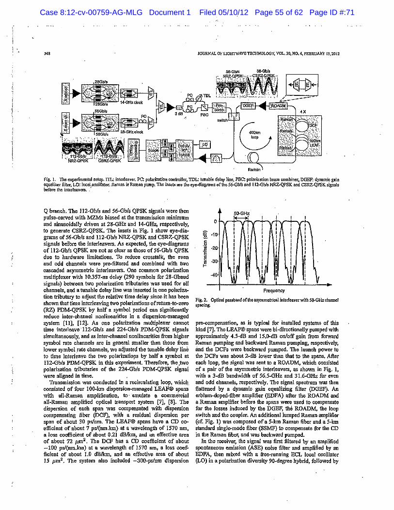
Case 8:12-cv-00759-AG-MLG Document 1 Filed 05/10/12 Page 55 of 62 Page ID #:71
'" JOURNAL OF LIOliTWAVE TECHNOLOGY, VOL. JO, NO, 4, FEBRUARY 15,2012
Fig. I. The experimental selup. ITI.: inteJ!eaver. PC: polarization controller, IDL: hmable delay line, PBC; polarization beam combiner~ DGEF; dyll!lmic gain equali:zcr filter, LO: local,oscilra1ar. Raman i:J Raman pump. The insets IU"~ the eye-diagrams of the 56-Gbfs and li2~Gbls NRZ-QPSK and CSRZ-QPSK signals before the interlcavern . . ' . '
Q branch. The 112-Gb/sand 56-Gb/s QPSK signals were then pulse-carved with MZMs biased at the transmission minimum and sinusoidally driven at 28-GHz and 14-GHz, respectively, to generate CSRZ-QPSK. The insets in Fig. 1 show eye-diagrams of 56-Gb/sand 112-Gb/s NRZ-QPSK and CSRZ-QPSK signals before the interleavers, As expected, the eye~diagrams of 112-Gb/s QPSK are not as clear as those of 56-Gb/s QPSK due to hardware limitations. To reduce crosstalk, the even and odd channels were pre-filtered and combined with two cascaded asymmetric interleavers. One common polarization multiplexer with 10.357-ns delay (290 symbols for 28-Gbaud signals) between two polarization tributaries was used for all channels, aqd a tunable delay line was inserted in one polarization tributary to adjust the relative time delay since it has been shown that time interleaving two polarizations ofretumwtowzero (RZ) PDM-QPSK by half a symbol period can significantly reduce inter-channel nonJinearities in a dispersion.;.managed system (11], [12]. As one polarization multiplexer cannot time interleave ·112-Gb/s and 224-Gb/s PDM-QPSK signals simultaneously, and as inter-channel nonlinearities from higher symbol rate channels arc in general smaller than those from lower symbol .rate channels, we adjusted the tunable delay line to time interleave the two polarizatiops by half a symbol at 112-Gb/s PDM-QPSK in this eXperiment. Therefore, the.two polarization tributaries of the 224-Gb/s PDM-QPSK signal were aligned in time.
Transmission was conducted in a recirculating Joop, which consisted of fuur 1 00-km dispersion•monaged LEAF® spans with allwRaman amplification, to· ·emulate a commercial all-Raman amplified optical transport system (7], [8]. The dispersion of each span was compensated with dispersion compensating fiber (DCF), wiih a residual dispersion per span of about 30 ps/nm. The LEAF® spans have a CD coefficient of about 7 ps/(nm.km) at a wavelength of 1570 nm, a loss coefficient of about 0.21 dB/km, and an effective area of about 72 pm2 • The DCF has a CD coefficient of about -100 ps/(nm.km) at a wavelength of 1570 nm, a loss coefficient of about I .0 dBikm, and an effective area of about lS p.m2 . The system also fncluded -3QQ .. ps/nm dispersion
SI).GHz
'-!:1.. ..L I ..L ~ 0 I I I I I I I I
-10 I I I I I I I I I I I I I I I I
-20 I I I I .I I I I I I
-30 I I I I I I
~ I
~ I I
\ I I
" ·40 I I
I I i
Frequency
Fig. 2. Optical pa$$band of the asymmetrical interfeaverwith SO·Gflz channel spacing.
pre-compensation, as is typical fur installed systems of this kind [7]. The LEAF® spans were bi-directionally pumped with approximately 4.5-dB and 15.0-dB on/off gain from forward Raman pumping and backward Raman pumping, respectively, and the DCFs were backward pumped. The launch power to the .DCFs was about 2-dB lower than that to the spans. After each loop, the signal was sent to a ROADM, which consisted of a pair of the asyrrnnetrJc interleavers, as shown in Fig. 1, with a 3-dB bandwidth of 56.5-GHz and 31.6-GHz for even and odd channels, respectively, The signal spectrum was then flattened by a dynamic gain equalizing filter (DGEF). An erbium-doped-fiber amplifier (BDFA) after the ROADM and a Raman amplifier before the spans were used to compensate for the losses induced by the DGBF, the ROADM, the loop switch and the coupler. An additional Jumped Raman amplifier (cf. Fig. 1) was composed of a 5-km Raman fiber and a 5-km standard single-mode fiber (SSMF) to compensate for the CD in the Raman fiber1 and was backward pumped,
In the receiver, the signal was first filtered by an amplified spontaneous emission (ASE) noise filter and amplified by an BDFA, then mixed with a free-running BCL local oscillator (LO) in a polarization diversity 90-degree hybrid, followed by

Case 8:12-cv-00759-AG-MLG Document 1 Filed 05/10/12 Page 56 of 62 Page ID #:72
XJE eta!.: TRANSMrSSJON OF MIXED 224-GB/SAND 1 J2·0B/S PDM·QPSK OVBR 1200-KMDISPERSION-MA'NAGIID LEAF® SPANS AND THREE ROADMS S49
ffi @. 0
]' -4 -~
Fig. 3. Pe!funnance in back-t~>-back configuration without (solid) and with (dashed IUld ()pen) 2 ROAOMs for 112-0bls.(a) and 224-Gbls (b) NRZ- and CSRZ·PDM-QPSK.
four balanced detectors with bandwidths of~ 40 GHz. The four. signal components were captured by two 2-channel 80-GSam· ples/s real-time oscilloscopes with 30-GHz bandwidths and an effective number of bits (ENoB) larger than 4.5 [13). For the 112-Gb/s PDM-QPSK, the oscilloscope bandwidth was reduced to 20-GHz. The captured signal was processed offline. The sampling skew was first corrected and the signal was synchronously re-sampled to 2 samples per symbol. After dispersion compensation, a butterfly equalizer with 19 taps, adapted via the constant modulus algorithm (CMA), was used for polarization demultiplexing (14], [15], residual dispersion compensation and· inter-symbcl interference ([Sl) mitigation. We found that 19 taps were sufficient to mitigate all the·ISI caused by residual CD, PMD, nonlinearity and filtering effects in our experiments. A phase increment frequency estimation algorithm was used for frequency estimation [16], and carrier phase estimation was performed using a decision-directed algorithm [17].
ill. REsULTS AND DISCUSSION
We first measured the tolerance towards narrow bandw width filtering of non-return-to-zero (NRZ) QPSK and CSRZ-QPSK. Fig. 3 shows the back·to-back performance without any ROADMs and with two ROADMs (i.e.; 4 ..Ymmetric interleavers) between the transmitter and the receiver. The 112-Gb/s and 224-Gb/s PDM-QPSK signals were set at an odd channel and an even channel, respectively. The figure shows that the performance of 112-Gb/s and 224-Gb/s· PDM-QPSK is slightly different with two ROADMs. Due
to hardware limitations, the 224-Gb/s PDM-QPSK requires 5-dB higher optical signal-to-noise-ratio (OSNR) than the 112-Gb/s PDM-QPSK when there is no ROADM, This reflects 'a 2-dB higher implementation penalty at 56 Gbaud compared to 28 Gbaud. In the back-to-hack case without ROADMs, CSRZ-PDM-QPSK requires. about 1-dB higher OSNR than NRZ-PDM-QPSK at bit-error-ratio (BER) of 10-• for both the 112-Gb/s and 224-Gb/s signals. This is· because that CSRZ-PDM-QPSK has a wider bandwidth than NRZ-PDM-QPSK and !hat !he receiver with its limited band· width cannot capture the entire signal spectrum. After the two ROADMs, the performance ofNRZ-PDM-QPSK is degraded, but the performance of CSRZ-PDM-QPSK Is improved, The improvement for 224-Gb/s CSRZ-PDM-QPSK is much larger than that for 112-Gb/s CSRZ-PDM-QPSK- For 224-Gb/s CSRZ·PDM-QPSK, the required OSNR at a BER of l0-3
is reduced by about 2.5 dB after two ROADMs compared to that without ROADMs and is about 2.5 dB less than that for 224-Gb/s NRZ·PDM-QPSK after two ROADMs. We also note that 224-Gb/s NRZ-PDM-QPSK has a higher error floor than 224-Gb/s CSRZ-PDM-QPSK. In contrast, for 112-Gb/s CSRZ·PDM-QPSK, the required OSNR at a BER of 10-3 is reduced only by ai:>out 0.5 dB after two ROADMs compared to that without ROADMs and is close to that for 112-Gb/s NRZ-PDM-QPSK after two ROADMs. We further found that the best performance can be achieved for IIZ..Gb/s and 224-Gb/s CSRZ-PDM-QPSK after four and three ROADMs, respectively, but for NRZ-PDM-QPSK, a higher penalty is induced when there are more ROADMs (not shown here). Note thatthe optimum number of ROADMs depends on the signal spectrum, tho ROADM characteristics, and the receiver response. Fig. 3 clearly indicates that CSRZ-QPSK can tolerate much narrow~>r filtering than NRZ-QPSK.
The results in Fig; 3 can be explained by the spectra of the signals, which are given in Fig. 4. The ROADM passbands of tho odd and even channels are also shown in the figure for reference. The normalized bandwidth of224-Gb/s NRZ·PDMQPSK is narrower than that of 112-Gb/s NRZ-PDM·QPSK. Due to the bandwidth limitation of tho 224-Gb/s data modu· Ialor, after tho pulse carver, the spectrum of 224-Gb/s CSRZPDM-QPSK spectrum has a dip in the middle. This is similar to transmit-side equalizati9n and helps to make the overall spectrum flat after filtering at both transmitter and receiver, which is beneficial fur narrow bandwidth filtering (5], The spectra in the figure also explain why we used CSRZ modulation here. A CSRZ pulse carver generates two tones ifhigher hannonics are neglected, so the spectrum of a CSRZ modulation is the convolution of the data spectrum ftom the data modulator and the two tones from 1he CSRZ pulse carver. Therefore. the shape of the overall spectrum can be easily control.led by changing the bandwidth of the data spectrum to make it flat-top or V -shaped, as shown by the spectra of the 112-Gb/s and 224-Gb/s CSRZPDM-QPSK, which has a significant impact on the signal's tolerance to filtering.
· The negative penalty of the 224-Gb/s CSRZ-PDM-QPSK comes ;pat1;1Y: from the excessive bandwidth of the original CSRZ signal and partiy from the shape of the ROADM passband, For. 112-Gb/s CSRZ-PDM-QPSK, as the normalized bandwidtb'ofthe data modulator is wider, there is no dip in the middle of the spectrum, but it has a much flatter top than that
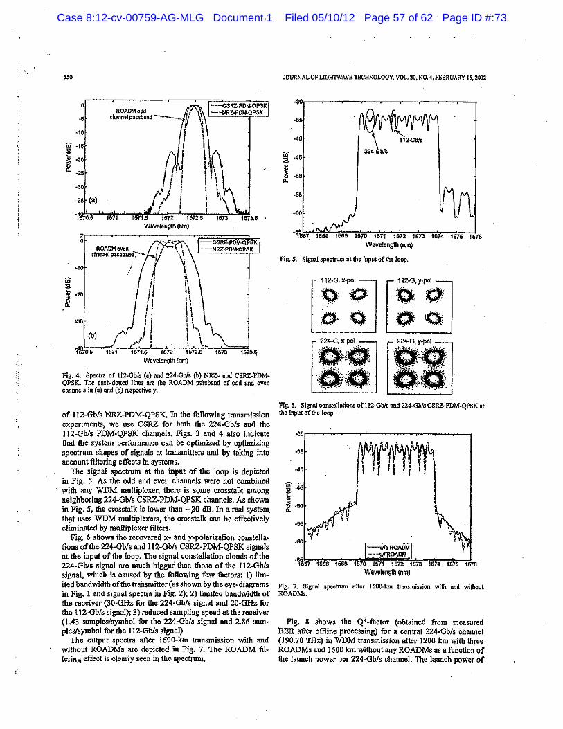
Case 8:12-cv-00759-AG-MLG Document 1 Filed 05/10/12 Page 57 of 62 Page ID #:73
S50
0
·• ·10
m ~1s ~ ~ ·20 ~ ll- -2!5
·30
.ss (a)
"feiM 1571
ROAOM.,.,.IIrt charmel passb1111d:"-
i I . I II
•10 j' I' •' I I I' I• n I' II
Jl .,,t !
iil ~
I ••• '30
(b)
1\Pio.s 1671 1671,(:; 1672 1572.6 Wavelength (nm)
-CSRZ·PDM-OPSK ---NRZ..POM-OPSK
1573.5 .'
1673
Fig. 4. Spec1n\ of 112-Gb/:i (a) and 224-GI>Is (b) NRZ· ond CSRZ-PDMQPSK. The dash-dotted lines are the ROADM paSsband of odd and even channels in (a) and (b) respectively.
of 112-Gb/s NRZ-PDM-QPSK. In the following transmission experiments, we use CSRZ for both the 224-Gb/s and tho 112-Gb/s PDM-QPSK channels. Figs. 3 and 4 also Indicate that the system performance can be optimized by optimizing spectrum shapes of signals at transmitters and by taking jnto account filtering effects in systems.
The signal spectrum at the input of the loop is depicted in Fig. 5. As the odd and even channels were not combined with any WDM multiplexer, there is some crosstalk among neighboring 224-Gb/s CSRZ-PDM-QPSK channels. As shown in Fig. 5, the crosstalk is lower than -~0 dB. In a real system th~t uses WDM multiplexers, the crosstalk can be effectively eliminated by multiplexer filters.
Fig. 6 shows the recovered x- and y-polarization consteflations of the 224-Gb/sand 112-Gb/s CSRZ-PDM-QPSK signals at the input of the loop. The signal constellation clouds of the 224-Gb/s signa! are much bigger than those of the 112-Gb/s signal, which is caused by the following few factors: 1) fimiied bandwidth of !he transmitter (as shown by the eye-diagrams in Fig. 1 and signal spectra in Fig. 2); 2) limited bandwidth of the receiver (30-GHz for the 224-Gb/s signal and 20-GHz for the 112-Gb/s signal); 3) reduced sampling speed at the receiver (1.43 samples/symbol for the 224-Gb/s signal and 2.86 sam• pies/symbol for the 112-Gb/s signal).
The output spectra after 1600-km transmission with and without ROADMs are depicted in Fig. 7. The ROADM filtering effect is clearly seen in the spectrum.
JOURNAL OF L!GJITWAVE TeCHNOLOOY, VOL, 30, NO. 4,FEBRUARY tS, 2012
•SS
-60
·'!ts7 .. Uiea 1669 1670 1671 1s12 1&73 1614 1S75 1676 Wevelenglh (run)
Fig. S. Signal spectrum at the Input of the loop.
·Q'Q :A .. ,a· .. .~ .-
Fig. 6. Signal constellotions or 112-0b/a md 224-Gb/s CSRZ-PDM-QPSK at the input of the loop. '
••• til' ' .. g. -46 b ~ ... 0.
-so
.,~57 1668: 1569 1570 1571 1672 1573 1674 161'5 1616 Wavel~ngth (nm)
Fig. 7. Sigrwl speotrum Wier 1600-km transmission with and without ROAD Ms.
Fig. 8 shows the Q2-factor (obtained from measured BER after offline processing) for a central 224-Gb/s channel (190.70 THz) in WDM transmission after 1200 km with three ROADMs and 1600 km without any ROADMs as a function of the launch power per 224-Gb/s channel. The launch power of
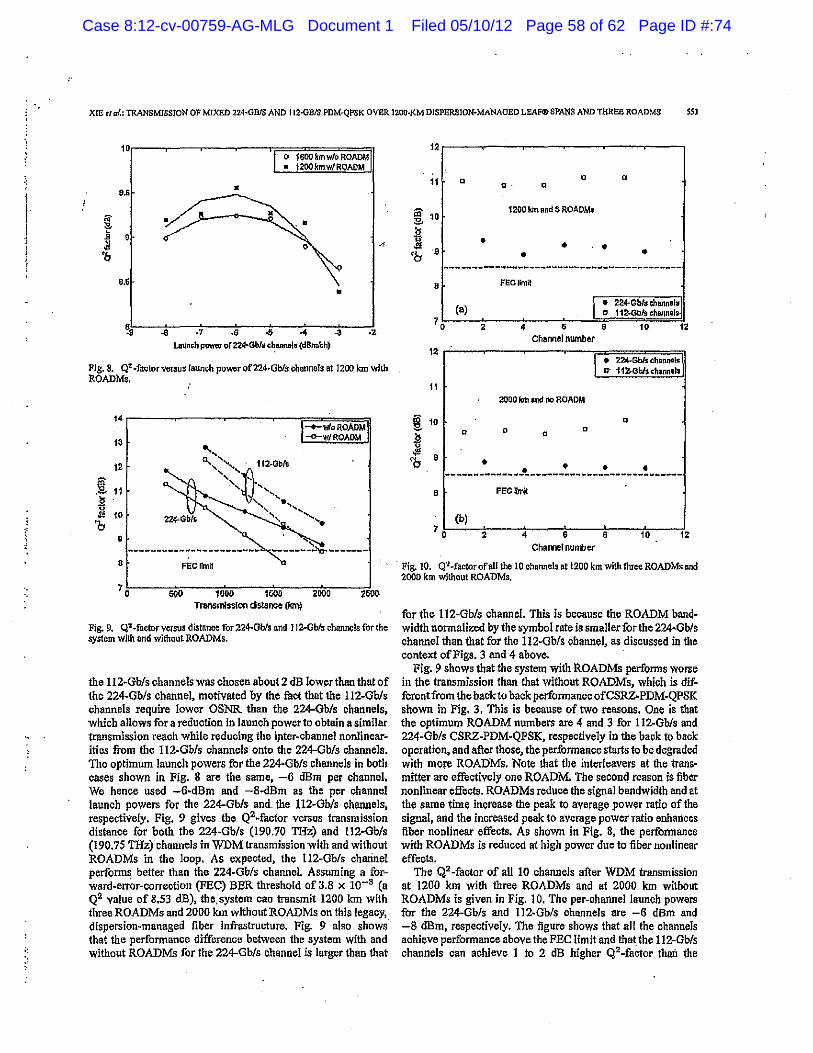
Case 8:12-cv-00759-AG-MLG Document 1 Filed 05/10/12 Page 58 of 62 Page ID #:74
' ' I I
1 '
XIE et r~l: TRANSMISSION OF MIXED 224·GBIS AND 112-GB/S PDM-QPSK OVER 1200-KM DlSPBRSION-MANAOED LEJ\FCIPSP~S AND THREE ROADMS 55J
10
·~
"' :&
j • '0
0.6 •
l.ftlln~h poweJ or224·Gb/s C~II.Dillt]IS (dBm/ch)
Fig, 8. Q2 -factorvors:us launch poV~Cr of224·Gbls: channels at 1200 Jon with ROADMs.
Fig. 9. Q2 -factor versus distance· for 224-Gb/s and J 12--Gbf:J channels for the system wilh and without ROADMs.
the 112·Gb/s channels was chosen about 2 dB lower than that of the 224-Gb/s channel, motivated by the fact that the II2-Gb/s channels require lower OSNR than the 224-Gb/s channels, which allows for a reduction in launch power to obtain a similar 1ransmission reach while reducing the ip.ter~channel nonlinear~ ities from the II2-Gb/s channels onto the 224-Gb/s channels. The optimum launch powers for the 224-Gb/s channels in both cases shown in Fig. 8 are the same, -6 dBm per channel-. We hence used -6·dBm and -8-dBm as the per channel launch powers for the 224-Gb/s and. the 112-0bfs channels, respectively. Fig. 9 gives the Q2 .. factor versus transmission distance for both the 224-Gb/s (190.70 lliz) and !12-0b/s (190.75 lliz) channels in WDMtransmission with and without ROADMs in the loop. As expected, the 112-Gb/s charinel perfonns better than the 224-Gb/s channeL Assuming a forward-error-correction (FEC) BER threshold of 3.8 x 10⁻³ (a Q2 value of 8.53 dB), the. system can transmit 1200 km with three ROADMs and 2000 km without ROADMs on this legacy, dispersion~managed fiber infrastructure. Fig. 9 also shows that the performance difference between the system with and without ROADMs for the 224-Gb/s channel is larger than that
• FECUmit
(a) l: 224-Gbl# chtutnllls 112-Gbf!l chaJJnels·
70 2 4 • • 10 12 enamel number
12 I • 22.4-Gbls t.h11nno~ o· 112-Gb/Hhanrzeb
11
2000 km e.nd no ROADM
10 a a 0 0
0
• • -~----------~-~-~-~--~------~------~YM ___ _ • FECI!rnit
(b) 7 o1r:..:..-;2c---T•--•.r---..--.,1';;o---}12
Charnel number
Fig. 10. Q'2-factorofall the 10 channels at 1200 km with 1luee ROADMsMd 2000 km without ROADMs.
for the 112·Gb/s channel. This is because the ROADM bandwidth normalized by the symbol rate is smaller for the 224·Gb/s channel than that for the ll2·Gb/s channel, as discussed in the context of Figs. 3 and 4 above.
Fig. 9 shows that the system with ROADMs perfonns worse in the transmission than that without ROADMs, which is different from the back to back perfonnanceofCSRZ-PDM·QPSK shown in Fig. 3. This is because of two reasons. One is that the optimum ROADM numbers are 4 and 3 for 112-0b/s and 224-0b/s CSRZ-PDM·QPSK, respectively In the back to back operation, and after those, the perfunnance starts to be degraded with mo(e ROADMs. Note that the interleavers at the trans· mitter are effectively one ROADM. The second reason is fiber nonlinear effects. ROADMs reduce the signal bandwidth and at the same time increase the peak to average power ratio of the signal, and the increased peak to average power ratio enhances fiber nonlinear effects. As shown in Fig. 8, the perfonnance with ROADMs is reduced at high power due to fiber nonlinear effects.
The Q'·factor of all 10 channels after WDM transmission at 1200 km with three ROADMs and at 2000 km without ROADMs is given in Fig. 10. The per-channel launch powers for the 224-Gb/s and 112-Gb/s channels are -6 dBm and -8 dBm, respectively. The fignre shows that all the channels achieve performance above the FEC limit and that the li2-Gb/s channels can achieve I to 2 dB higher Q2-factor than the
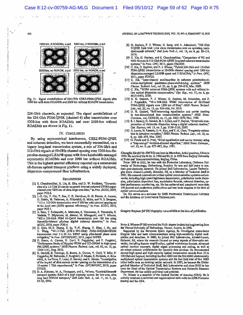
Case 8:12-cv-00759-AG-MLG Document 1 Filed 05/10/12 Page 59 of 62 Page ID #:75
552
Fig. II. Signal constellations of224-Gbls CSRZ-PDM-QPSK signals EJfter 1200 Jan with three ROADMs and 2000 km wilhout ROADM transmission.
224-Gb/s channels, 1as expected. The signal constellations of
the 224-Gb/s PDM;QPSK (channel 6) after transmission over 1200-km with three ROADMs and over 2000-km without ROADMs are shown in Fig. 11.
IV. CONCLUSION
By using .. ymmetrical interleavers, CSRZ-PDM-QPSK and coherent detection, we have successfully transmitted, on a legacy long-haul transmission system, a mix of 224-Gb/s and 112-Gb/s signals at 50-GHz channel spacing over 1200-km dispersion-managed LEAF® spans with three b~ndwidth-managed asymmetric ROADMs and over 2000 km without ROADMs. This is the highest spectral efficiency reported on a commercial all-Raman optical transport platfurm using a widely deployed, dispersion-compensated fiber infrastructure.
REFERENCES
[J] S. Chandrosckhar, X. Liu. B. Zhu, and D. W. Peckham, ''TrallSmis. slon of a l.Z.. Tbls 24-earrler no-guard intervol ooherent OFDM superchannel over720Cl-km of ultra-large-area tiber," in Proa •. ECOC, 2009, paper PDZ.6.
121 J.-X. Ca~ Y. Cai, Y. Sun, C. R. Davidson, D. 0. Foursa,. A. Lucero, 0. Sinkin,. W, Patterson, A. Pilipelskii, G. Mohs, ~nd N. S. Bergano, "'112 x 112 Gb/s tmmmission over 9 360 k:m with chMnol spacing set to the baud rnte (36{)% spectre! efficiency)," in Proc. ECOC, 2010, paper l'D2.1.
[3] A. Sane, T. Kobayashi, A. Matsuura, S. Yamamoto, S. Yamanaka,. B. Yoshida, Y. Miyamoto; M. Matsui, M. Mizoguchi, and T. Mizuno, "tOO x 120-Gb/.s PDM 64·QAM tmmmission over 160 km using Jlnewldcb·tolorant p.ilo(Je.g digital coherent detection," In Proc. ECOC, 2010, pap~r PD2~4.
[4] D. Qien, M.~F. Huru1g, E. lp, Y.-K. Huang, Y. Shao, J. Hu, and T. W•ns, "I01.7·Tbls (370 X 294·Gbls) PDM-IZ8QAM-OFDM transmission over 3 x SS km SSMF using pilot-based phase noise mitigation:• in Proc. OFC/NFOEC. 2011, paper PDPBS.
[5] G. BO!co, A. Catena. V. Curri, P. Poggiolini, and F. Forghieri, ''Performam:<: limits ofNyquist·WDM and CO-OFDM in high-spcOO PM~QPSKsystems," IEEE Photon. Techno/. Lett., vo(. 22, no, 15, pp. 11Z!H131, Aug. 2010.
[6] G. Gavioli. B. 'Tbrrengo, G. Bo:roo, A. Carene, V. Cuni, V. Miot, P. Poggiolini, M. Belmonle, F. Forghieri, C. Muzio, S. Piciaecia, A. Brin~ ciotti, A. La Porta, c. Lett~ s. SiiVory. and s. Abrotc. "Investigation ofthe impact ofultra-narrow carrier spacing on the transmission of a 10-carrier 1 Tb/s Supcn:hllflJiel," in Proc. OFCINFOEC, 2010, paper 0Th03.
(7] D. A. Fishman, W. A. Thompson, and L. Vallone, "LambdaXtreme® tranSport system: R&D of a high capacity system fbr low cost, ultra long haul DWDM tmnsport,.,. Bell Labs Ttch. J., vol. 11, no. 2, pp. 27-53, 2006.
JOURNAL OF LIOH'IWAVB TECHNOLOGY, VOL. 30, NO.4, FEBRUARY 15,2012
{8] G, Raybon, P. 1. Winv;r, H. Song, and A, Adamiecki, "100 Gb/.s DQPSK. field trial: Live video transmission over an operating Jambd:ax1r(lnle® network, .. Bell Lab$ Tech J., vol, 141 no: 4, pp. 85-114, 2010.
[9] C. Xie, G. Raybon, and S. Chandrasekhar, ''Comparison of RZ and NRZ formats in 112-Gbls PDM~QPSK loJlgha.ul coherenttntnsmission systems," in Proc. OFC, 2011, paper JThA039.
[tO] C. Xie, G. Raybon, and P. J. Winzer, "Hybrid 224-Gb/sand 112..Qb/s PDM-QPSK trnnsmtssion at 50-GHz channel spacing over 1200-km disporsion~managed LEAF® spans and 3 ROADMs," in Proc. OFC, 2011, paper PDPD2.
[llJ C. Xio, "Inter-channel nonlinearities in coherent polarlzation-dl~ visionMmultiplexed quadrature~phase-shift..keylng systems," lESE Photon. '{echnol. Lett., vol, 21, no. S~ pp. 274-276, Mar. 2009.
[12] C. Xie, "WDM cohen .. nt PDM-QPSK systems with and without in· Jino optioal dispersion compensntion," Opt. Exp., vol, 17, no. 6. pp .
. 48)5-4823, 2009. . [13] A. H. Gnauck, P, J. Wmzer, G. Raybon, M. Schnecker, and P,
J, Pupalaikls, '110 x 224-Gb/s WDM transmission of 56-Gbaud PDMMQPSK signals over 1890 km of fiber," IEEE Photo11. Technof. Lett., vo1 .. 22. no. 13, pp. 954-956. Jul. 2010.
[14] D. N. Godard, ''Solf-reooverlng equalization and carrier tracking in two--dimensional data communication systems/' IEEE Trans. Commun., vol, COM-28, no. II. pp. 1867-1875, Nov. 1980.
[lS] S. J. Savory, G. GaVioli,R.l. Killey, and F. Bayv11l, "Electronic com· pensation of chromatic dispersion using a digital coherent re~iver," Opt. Expre.rs, vel. IS, no, 5, pp. 2120-2126,2007.
{16] A. Leven, N. Kaneda, U.·Y. Koc, and Y.-K. Chen, "Frequency estimation in intradyne reception," IEEE Photon. TechnoL Lei!., vol, 19, no, 6, pp. 366-368, Mar, 2007.
{J7] G. Picchi and G, Pmti, "Blind equalization and carrier recovel)' using a "stop..and~go" decision-directed algorithm," IEEE 'lhln.r. Commun., vol. 35, no. 9, pp. 817-887, Scp. 1981.
ChongjloXie (M'Ol..SM'OS)was born in Maanshan, Anbul provinte, China in 1970. Ho rocoived his M.So. in 1 !196 and Ph.D. ln 1999fulm Beijing University ofPosts and Tclecommunloatfons, Beijing, China.
From 1 !i199 to 2001, he was with the Photonics Labomtory, Chalmers Unj.. versity of Technology. Gothenburg. Sv.oeden~ for one and half years to con~ duct post--doctorate research. He joined Bell Laboratories, Lucent Technologies (now AlcaM~Lucent}, Holmdel, NJ, as a Member of Technical Stoff In
. 2001. His research intere$13 are in fiber optical commllflication systems aP<l network:!, including high-speed lightwave transmission, polarization mode dispersiof\ pohuizR.tion dependent Joss, modulation I'Qnnats,. coherent detection, optical pc:rfonnance monitoring., etc. He has authored Md coauthored more than 150 journal and conference publicatfons and two book chapters in the field of optical communications.
Dr. Xie .serves llS n Jt:.viewer for IEEE PHOTONICS.T'ECHNOLOOY LJITrERS and the JOURNAL OP LlGHTWAVB TECHNOLOGY,
Gregory ltaybon (M'OO) biography not available at the time of publication.
l'eter J. Wlnzer(F'09) received the Ph.lJ. degree in electrlcalengineeringfiom the VIenna University ofThchnology, Vienna, Austria, in 1998.
Supported by the European Space Agency, he investigated space-borne Doppler lidar An~ laser communicatiQns using high-sensitivity digital modulation and detection. In 2000. he joined Bell Labonuories-, Alcatel~Lucent, Holmdel, NJ, where his research focused on many aspects offib~-optic networks, Including Raman amplification, optical modulation fonnaiS, advanced optical receiver concepts, digital signal processing und coding. as well 113 on robust netWork architectures for dynamic data services. He demonstroted' several high-speed and high-capacity optical trammission records ftom 10 to 100Gb/sand beyond, including the :first tOOG and the first 4000 electronically multiplexed optical transmission systems and the first field trial of live lOOG video traffic over t~n existing carrier network. In 2007, he became lhe Dislingqished Member of Technical Staff, Bell Laboratories and since 2010 ho has been the Head of tile Optical Transmission Sys1ems and Networks Research Department. He has widely published and patented.
Dr. Winzer is a member of the Optical Society of Amerit::a (OSA). He is actively involved in technical and organizational tasks with the lBEB Photonics society and the OSA.
Case 8:12-cv-00759-AG-MLG Document 1 Filed 05/10/12 Page 60 of 62 Page ID #:76
UNITED STATES DISTRICT COURT CENTRAL DISTRICT OF CALIFORNIA
NOTICE OF ASSIGNMENT TO UNITED STATES MAGISTRATE JUDGE FOR DISCOVERY
This case has been assigned to District Judge Andrew Guilford and the assigned discovery Magistrate Judge is Marc Goldman.
The case number on all documents filed with the Court should read as follows:
SACV12- 759 AG (MLGx)
Pursuant to General Order 05-07 of the United States District Court for the Central District of California, the Magistrate Judge has been designated to hear discovery related motions.
All discovery related motions should be noticed on the calendar of the Magistrate Judge
--------------------~==-~=~----
NOTICE TO COUNSEL
A copy of this notice must be served with the summons and complaint on all defendants (if a removal action is flied, a copy of this notice must be served on all plaintiffs).
Subsequent documents must be filed at tile following location:
U Western Division 312 N. Spring St., Rm. G-8 Los· Angeles, CA 90012
[X] Southern Division 411 West Fourth St., Rm.1-053 Sant~ Ana, CA 92701-4516
Failure to file at the proper location will resu"!t In your documents being returned to you.
U Eastern Division 3470 Twelfth St., Rm. 134 Riverside, CA 92501
CV-18 (03/06) NOTICE OF ASSIGNMENT TO UNITED STATES MAGISTRATE JUDGE FOR DISCOVERY
Case 8:12-cv-00759-AG-MLG Document 1 Filed 05/10/12 Page 61 of 62 Page ID #:77
UNITED STATES DISTR!Cf COURT, CENTRAL DISTRICT OF CALIFORNIA CIVIL COVF.R SHEET
! (a) PLAINTIFFS (Check box if you Me representing yourself D) La.byrinth Optical Technologies LLC
(b) Attorneys (Finn Name, Address and Telephone Number.lfyou are representing yourself, provide same.)
Shnmont Browder0ianari3 Angclides& Barnerd LLC, tOO N. Sepulveda Blvd,, Suite 1350, El Se.gundn1 CA 90245; Tel. 310.322.3555 ·
DEFENDANTS Alcatei-Luccm USA, Inc.
Attorneys (If Known)
U. BASIS OF JURISDlCTION (Place an X in one box only.) ffi, CITIZENSRJ:P OF PRINCIPAL PARTIES- For Diversity Cases Only (Place an X in one box. for plaintiff and one for defendant)
D ) U.S. Oovemmenll)lainliff lilf 3 Federal Question (U.S. PTP DEF I'TF DEP Govcmment Not a Party) Citizen ofThis State 01 01 lncorporat:d or Principal Place 04 04
of Business in this St:ate
0 2 U.S. Govcrnm~t Otfcndanf 0 4 Diversity (Indicate Cltizensbip Citizen of Another State 02 02 Cncorporutod and Printipal Place 05 05 of Parties in Hem m) ofBusiness in Another S1ate
Citizen or Subject ofll Foreign Country D 3 D 3 Foreign Nation
IV. ORIGIN (Piace.IUlXinoncboxonfy.)
lit Original o 2 Removed from D 3 Remanded from [J 4 Reinstated or 0 S Tnmsferred l'rom another dis11ie1 (specifY): Proceeding Slate Cou(l App~llatc C(lurt Reopened
V. REQUESTED IN COMPLAlNT: JURY DEMAND: iYcs 0 No (Chec:k 'Yes• only iftlem;~.nded In eomplulnt}
CLAsS .ACTION u.P.de~ F.R.C.P. 23: DYes rlf'No 0 MONEY l;t~ANDED IN COMPLA JNf: S
06 MultiDistrict Litigation
06 06
0 7 Appe1d to District Judge from Mugistr!.te Judge
VI. CAUSE OF ACI'JON (Cite the U.S. Civil Stntulr: underwhicb you arc filing end write a brief statement of cause. Oo not cite jurisdictional statutes unless diversity.)
Palen! Infringement
0410 Antitrust Marine 0 430 Bam lui and Banking 130 Miller Act 0 450 CommCI'C(:IICC 140 Negotiable Imtrument
Rat.cs/etc. 150 Recovcryof 0 460 Deportation OVerpayment & 0 470 Racketeer Infloonced Enforcement of
and Corrupt Judgment Organizations Medicare Act
D 480 Consumer Credit Rcoovet)' ofDefauUcd 0 490 CableJSn.t TV Student Loan {Excl. U RlO Selective Service Vetenlns) D 8$0 Sec>utiitios/Cc>!Tll1nodlit~s/ 110 153 Recovery of
Exchange Overpaymem of 0 875 Cuslomc~ Challenge 12 Veteran~& Bcneflts
USC 3410 160 Stookholder!' Suit' D 890 OtherStatulory Actiol'l3 190 Other Contract 0 891 AgricultWltl Act 195 Contract Produ~ 0 89:2 Bconomlc Stabilit~don
Act 0 893 BovironmenLBI Matters 0 894 Energy Allocation Act 0 895 Freedom of Info. Act 0 900 Appeal of F<:c Oetcrmi-
nation Under Equal Acc~s to Justice
0 950 Constitutionality (If State Stabiles
Fo~closure
Rent Le&se & Bjectml:'nl Tort.s to land Tort Product Liabitlly All Other Real Property
"] &; .
630 I:.iquor Lav.'S 640 R.R. & Truck 650 Airline Regs 660 Occupational
Safety IH~:alth 690 Other
r~i FORO~CEUSEONLY: CMeNUm~r.------------------~--------~a-~~~·~--~--------·
i Act l.ebodMgmt. Relations
730 Labor/Mgml Reporting & Disclosute Act Railway Labor Act Othcrlllbor
AFTER COMPLETfNG TIJE FRONT SlD'E OF FORM CV-?1, COMPLETE THE INFORMATION REQUESTED BELOW.
CV-71 (05,08) CIVIL COVERSIIEET Pagel of2

Case 8:12-cv-00759-AG-MLG Document 1 Filed 05/10/12 Page 62 of 62 Page ID #:78
UNITED STATES DISTRICT COURT, CENTRAL lllSTR!CT OF CALIFORNIA CfVJI, COVER SHEET
Vlll(n), IDF:i\'TICALCASF-~: II as this action been previously filed in this court and dismissed, remMHkd or clo~~:d'f fiNo 0 Yes
If yes, list case numbct(s): -------------------------------------------------
VJII(b). RELATED CASKS: H!IVe any cases betn prc\'iously tiled in this court that nre relnted to the present ~;Use? M'No 0 Yes
Jfyes,lisl c:ue number(s): ----------------------------------------------
Civil cn.~es ltn: deemed related If a previously filed case nnd ibn pre,ent cnse:
{Check all boxes thtll apply} 0 A, Arise from the same or closely telatctilnmsactions, happenlng..-t, or~vents; or
D B. Call for determination oithe same or substnmially rei:~ ted or similar (]Uestians of law and fuct; or
0 C. I; or other roo~ons would entail subslantial duplication of IDbor if heard by different judges; or
D D. Involve the s:tme patent, trudemnrk orcopyrieht, !llll! one of the i'aclors identified nbavc in 11, b or c also is present.
[X, VENUE: (When completing the followintt information, usc an additional sheet ifnetes!lu.ry.)
{a) Lisl the County in this District~ Cu\ifomln County outside ofihis District; State ifolher thlln California;- or Foreign Count:ty, in which EACIJ ruuned plaintiff resides If this box is checked, ~o to ncm rbt 0 Check here if the government it:s a •cnde.~ or emn!ovees is a named Plaintiff.
County in this Oisnict;• California County oulside of this District; State, irothcrlhan Cali(om!a; or Porcign Country
Orange County
c'
(b) Ustthc County in this Disrrict; Cnlifomia County outside of this Disuict; State if other than Ct~!ifomia; or Foreign Country, in which EACH named defendant rcstdcs. 0 Check here if the gpvcmm(:nt, its a~encies orernolovees is a nllmed defendnnt. lftl1is box is checked, g<J to item (c),
County in this Di~tdct:• California (',ounty outside ofthi11 District; Stale, if other thlln Co.liromin; or Foreign Country
D' " ., ' (
J, _, ·~ '
{c) List the County in this District; California County outside ()fthis District; State ifothet tlmn California; or Foreign C{)untry, in which EACH<:It:llm arose. N t I 1 d d t' ncasd wcfh! cudcn'loftbtt t (J dl olv d o e: ... CUll ClnflM 10 . ' 0 "" . '"' "' ' '
County m this DiS1rlct:• California County outs We oflhil: District; State, if other thM Clllfomia; or Iton:ign Country
~
l-, ~' '! ;'. ', ' ' I' ~i
;, Uls Angeles, On.nge, San Bernnrdlno, Hlven;id~, Ventura, Snnla ful.rbarn, or San Luis Obispo Counties Nott: tn land cond nlltio us.e th I ion of the tract ofllmd i vo ved
Notice lo ConnseVParlies: The CV-71 {JS.44) Civil CoverS cd herein neither replace nor supplemenl the filing und servireofpleadings or other papers as requiretl hy !:nv. This form, approved by the J nnfcrence orthc States in September 1974, is required pursuunt to Local RuJc l-1 Is nQifiled but is u.'>Cd by the C!crk of the Court for the purpo..~e of statistics, venue and initiating the civil docket sheet. (for more detailed inmuction.~. see separate instructions sheet.)
Key to Statistical codes rcluting to Social Security Cu:ws:
Nature of Suit Code Abbtcviatinn
86! H!A
862 BL
863 rl!WC
863 DIWW
1164 SS!D
,., RSI
CV-71 (05/08}
Subshntlve Statement or Can.>te o( Action
All cluims for heulth lnsuroncc benefits (Medicare) ut~der'rltle 1 B, Part A, of the Social Security Act, 115 amended. Also, include claims by hospitals, skilled nursing facilities, etc., for certification ns providers of sCT'Vlces under the pmgnun. (42 U.S.C, 193SFF(b))
All da!ms for"Dlack Lung'' benefit! under Title 4, Pan B, of the Ferlcrnl Coal Mine Health and Safety Act of 1969. (30 u.s.c. 923)
All claims filed by insurCd workers f(lr disability insurnnct benefit= under Title 2 of the Social Security Act, t:s amended; plus all claims filed for child's in~unmce bene tits based on disability. (42 U.S.C. 405(g))
All duims filed for widows or widowers insurnnce benefits bus..-:d on disability under Title 2 of the SociAl Security Act, as :tmended. (42 U.S.C. 405(g))
All claims for supplemental security income payments based upori disability filed under Title 16 of the Socia! Set:urity Act, 1lli amended.
All claim.1 for lttilcment (old nge) and survivors bencfiu undct Titlc2 of the Social Securil)' Act, as amended (42 U,S,C. (g))
CIVIL COVER SHEET Page 2 of2