Embed Size (px)
Citation preview
1013/SY/Pre_Pap/Elec/EDC_Soln54
Vidyalankar S.Y. Diploma : Sem. III
[EJ/EN/ET/EX/EV/ED/IU/DE/IS/IC/IE/MU] Electronics Devices and Circuits
Prelim Question Paper Solution
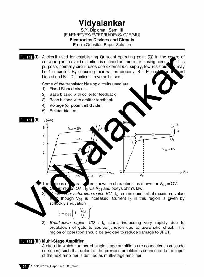
(i) A circuit used for establishing Quiscent operating point (Q) in the centre of active region to avoid distortion is defined as transistor biasing circuit. For this purpose, normally circuit uses one external d.c. supply, few resistors and may be 1 capacitor. By choosing their values properly, B E junction is forward biased and B C junction is reverse biased.
Some of the transistor biasing circuits used are 1) Fixed Biased circuit2) Base biased with collector feedback3) Base biased with emitter feedback4) Voltage (or potential) divider5) Emitter biased
(ii)
The regions of operation are shown in characteristics drawn for VGS = OV. 1) Ohmic region OA : ID v/s VDS and obeys ohm’s law.2) Pinchoff or saturation region BC : ID remain constant at maximum value
even though VDS is increased. Current ID in this region is given byschockly’s equation
2GS
D DSSP
VI I 1
V
3) Breakdown region CD : ID starts increasing very rapidly due to
breakdown of gate to source junction due to avalanche effect. This region of operation should be avoided to reduce damage to JFET.
(iii) Multi-Stage Amplifier A circuit in which number of single stage amplifiers are connected in cascade (in series) such that output of the previous amplifier is connected to the input of the next amplifier is defined as multi-stage amplifier.
1. (a)
1. (a)
VDS
ID (mA)
IDSS A
B C1
D
â
ä
VP O
VGS = 0V
VDS 5 10 15 208 250
ID (mA)
1
2
3
4
5 VGS = 0V
1V
2V
3V
4V
ã
1. (a)
Vidyala
nkar
Prelim Question Paper Solution
1013/SY/Pre_Pap/Elec/EDC_Soln 55
A single stage voltage amplifier is not capable of giving too large voltage gain. Sometimes input signals are very weak, in such cases they are required to be amplified more. For this purpose multi-stage amplifiers are used.
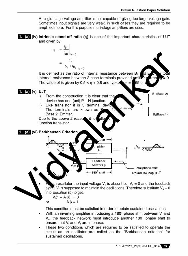
(iv) Intrinsic stand-off ratio () is one of the important characteristics of UJT and given by
= 1
E
B
BB I 0
r
r
= 1
1 2 E
B
B B I 0
r
r r
It is defined as the ratio of internal resistance between B1 and E to the total internal resistance between 2 base terminals provided emitter current IE = 0. The value of is given by 0.5 < < 0.8 and typically = 0.65 or o.7.
(v) UJT i) From the construction it is clear that the
device has one (uni) P N junction. ii) Like transistor it is 3 terminal device.
The terminals are known as Base 1, Base 2, Emitter.
Due to the above 2 reasons it to called uni-junction transistor.
(vi) Barkhausen Criterion
For an oscillator the input voltage Vs is absent i.e. Vs = 0 and the feedback signal Vf is supposed to maintain the oscillations. Therefore substitute Vs = 0 into Equation (5) to get,
Vi(1 A ) = 0 or A = 1
This condition must be satisfied in order to obtain sustained oscilations. With an inverting amplifier introducing a 180 phase shift between Vi and
Vo, the feedback network must introduce another 180 phase shift to ensure that Vi and Vf are in phase.
These two conditions which are required to be satisfied to operate the circuit as an oscillator are called as the "Barkhausen criterion" for sustained oscillations.
1. (a)
1. (a) B2 (Base 2)
B1(Base 1)
E (Emitter)
1. (a)
Vidyala
nkar
Vidyalankar : S.Y. Diploma EDC
1013/SY/Pre_Pap/Elec/EDC_Soln 56
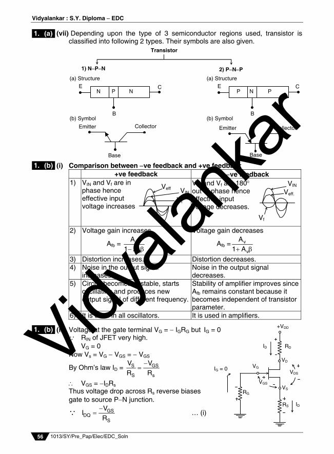
(vii) Depending upon the type of 3 semiconductor regions used, transistor is classified into following 2 types. Their symbols are also given.
(i) Comparison between ve feedback and +ve feedback +ve feedback ve feedback 1) VIN and Vf are in
phase hence effective input voltage increases
VIN and Vf are 180 out of phase hence effective input voltage decreases.
2) Voltage gain increases
Afb = v
v
A1 A
Voltage gain decreases
Afb = v
v
A1 A
3) Distortion increases. Distortion decreases. 4) Noise in the output signal
increases. Noise in the output signal decreases.
5) Circuit becomes unstable, starts oscillating and produces new output signal of different frequency.
Stability of amplifier improves since Afb remains constant because it becomes independent of transistor parameter.
6) It is used in all oscillators. It is used in amplifiers.
(ii) Voltage at the gate terminal VG = IGRG but IG = 0 RIN of JFET very high. VG = 0 Now Vs = VG VGS = VGS
By Ohm’s law ID = S GS
S s
V VR R
VGS = IDRs Thus voltage drop across Rs reverse biases gate to source PN junction.
GS
DQS
VI
R
… (i)
1. (a)
1. (b)
Veff
Vf VIN Veff.
VIN
Vf
1. (b)
ID RD
+VDD
IG = 0
RG
VG VD
VS
VDS
VGS
ID RS
Transistor
2) PNP 1) NPN
(a) Structure
N P N
B
E C P N P
B
E C
(a) Structure
(b) Symbol
Collector Emitter
Base Base
(b) Symbol
Collector Emitter
Vidyala
nkar
Prelim Question Paper Solution
1013/SY/Pre_Pap/Elec/EDC_Soln 57
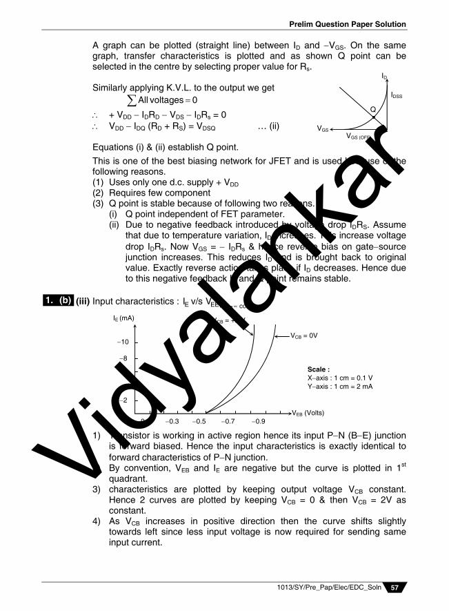
A graph can be plotted (straight line) between ID and VGS. On the same graph, transfer characteristics is plotted and as shown Q point can be selected in the centre by selecting proper value for Rs. Similarly applying K.V.L. to the output we get All voltages 0
+ VDD IDRD VDS IDRs = 0 VDD IDQ (RD + RS) = VDSQ … (ii) Equations (i) & (ii) establish Q point.
This is one of the best biasing network for JFET and is used because of the following reasons. (1) Uses only one d.c. supply + VDD (2) Requires few component (3) Q point is stable because of following two reasons.
(i) Q point independent of FET parameter. (ii) Due to negative feedback introduced by voltage drop IDRS. Assume
that due to temperature variation, ID increases. This increase voltage drop IDRs. Now VGS = IDRs & hence reverse bias on gatesource junction increases. This reduces ID and is brought back to original value. Exactly reverse action takes place if ID decreases. Hence due to this negative feedback ID and Q point remains stable.
(iii) Input characteristics :
CBE EE V constantI v/s V
1) Transistor is working in active region hence its input PN (BE) junction is forward biased. Hence the input characteristics is exactly identical to forward characteristics of PN junction.
2) By convention, VEB and IE are negative but the curve is plotted in 1st quadrant.
3) characteristics are plotted by keeping output voltage VCB constant. Hence 2 curves are plotted by keeping VCB = 0 & then VCB = 2V as constant.
4) As VCB increases in positive direction then the curve shifts slightly towards left since less input voltage is now required for sending same input current.
IDSS
VGS (OFF)
VGS
ID
Q
1. (b)
2
VCB = +2 V
VCB = 0V
VEB (Volts) 0.1 0.3 0.5 0.7 0.9
4
6
8
10
IE (mA)
Scale : Xaxis : 1 cm = 0.1 V Yaxis : 1 cm = 2 mA
Vidyala
nkar
Vidyalankar : S.Y. Diploma EDC
1013/SY/Pre_Pap/Elec/EDC_Soln 58
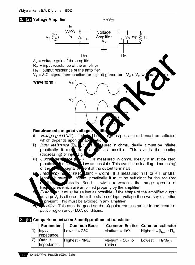
Voltage Amplifier AV = voltage gain of the amplifier RIN = input resistance of the amplifier RO = output resistance of the amplifier VS = A.C. signal from function (or signal) generator VO > VIN without distortion
Wave form :
Requirements of good voltage amplifier : i) Voltage gain (AV) : It should be as high as possible or It must be sufficient
which depends upon the application. ii) Input resistance (RIN) : It is measured in ohms. Ideally it must be infinite,
practically it must be as high as possible. This avoids the loading (decreasing) of input signal.
iii) Output resistance (RO) : It is measured in ohms. Ideally it must be zero, practically it must be as low as possible. This avoids the loading (decreasing) of the voltage signal present at the output terminals.
iv) Frequency response (or Band width) : It is measured in Hz or KHz or MHz. Ideally it must be infinite, practically it must be sufficient for the required application. Basically Band width represents the range (group) of frequencies which are amplified properly by the amplifier.
v) Distortion : It must be as low as possible. If the shape of the amplified output voltage V0 is different from the shape of input voltage then we say distortion is present. This must be avoided in any amplifier.
vi) Stability : This must be good so that Q point remains stable in the centre of active region under D.C. conditions.
Comparison between 3 configurations of transistor
Parameter Common Base Common Emitter Common collector 1) Input
impedance Lowest 25 Medium 1k Highest = D.C RE
2) Output Impedance
Highest 1M Medium 50k to 100k
Lowest = RE/D.C.
2. (a)
VS
RIN
i/p
Voltage Amplifier
AV
VIN
RS
+
+VCC
VO
RO
o/p RL
2. (b)
VIN
t
VO
t
Vidyala
nkar
Prelim Question Paper Solution
1013/SY/Pre_Pap/Elec/EDC_Soln 59
3) Current gain D.C 1 lowest 100 < D.C. < 500 high
(D.C. + 1) Highest
4) Voltage gain High Highest Less than 1 lowest 5) Power gain Moderate Highest Medium 6) Leakage
current ICBO = ICO lowest 5 A for Ge, 1A for Si
ICEO = D.C.ICBO High 500A for Ge, 20A for Si
ICEO High 500A for Ge, 20A for Si
7) Phase shift 0 (In phase) 180 (out of phase)
0 (In phase)
8) Cut-off frequency
High Lower than CB Depends upon load
9) Thermal stability
High Low High
10) Applications For high frequency For audio frequency For impedance matching as a buffer.
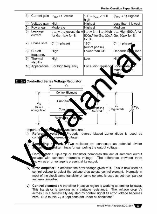
Controlled Series Voltage Regulator
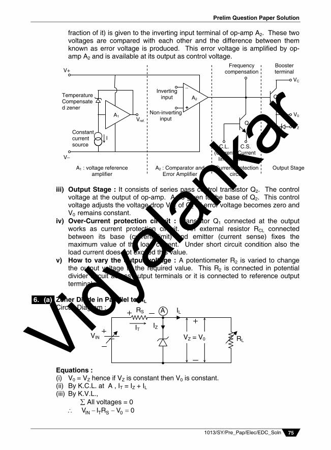
Important blocks and their functions are : i) Reference voltage : Properly reverse biased zener diode is used as
constant D.C. reference voltage.
ii) Sampeling network : Two resistors are connected as potential divider across the output terminals for sampeling the output voltage.
iii) Comparator : Opamp or transistor compares the actual sampled output voltage with constant reference voltage. The difference between them known as error voltage is present at its output.
iv) Error Amplifier : It amplifies the error voltage given to it. This is now used as control voltage to adjust the voltage drop across control element. Normally in most of the circuit same transistor or same opamp is used as both comparator and error amplifier.
v) Control element : A transistor in active region is working as emitter follower. This transistor is working as a variable resistance. The voltage drop VS across it is automatically adjusted by control signal till error voltage becomes zero. Due to this V0 is kept constant under all conditions.
2. (c)
Error Amplifier
Comparator
Reference voltage
Control Element
Sampeling Network
VIN (D.C.)
unregulated
VS +
+
V0 (Regulated) RL
Vidyala
nkar
Vidyalankar : S.Y. Diploma EDC
1013/SY/Pre_Pap/Elec/EDC_Soln 60
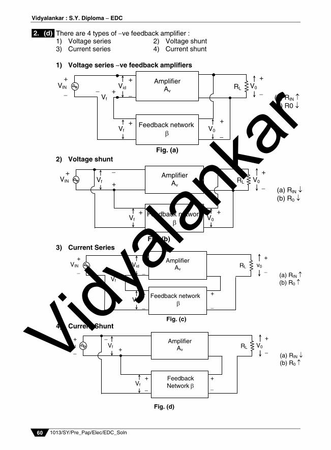
There are 4 types of ve feedback amplifier : 1) Voltage series 2) Voltage shunt 3) Current series 4) Current shunt
1) Voltage series ve feedback amplifiers
2) Voltage shunt
3) Current Series
4) Current Shunt
2. (d)
Amplifier Av
Feedback network
+
+
VIN +
Vid V0
Vf V0 +
RL + Vf
+
(a) RIN (b) R0
Fig. (a)
Fig. (b)
Amplifier Av
Feedback network
+
+
VIN
+ Vf V0
Vf +
RL
+
(a) RIN (b) R0
V0
Fig. (c)
Amplifier Av
Feedback network
+
+
VIN
Vf
v0
Vf +
RL
+
(a) RIN (b) R0
+
Vid
Fig. (d)
Amplifier Av
Feedback Network
+
+
VIN +
Vf V0
Vf +
RL
+
(a) RIN (b) R0
Vidyala
nkar
Prelim Question Paper Solution
1013/SY/Pre_Pap/Elec/EDC_Soln 61
Note : (i) An ammeter is connected in series while voltmeter is connected in parallel. (ii) Hence at the output if it is parallel connection then it is voltage feedback and
if it is series connection then it is current feedback. (iii) Similarly at the input if it is series connection then it is series feedback and if
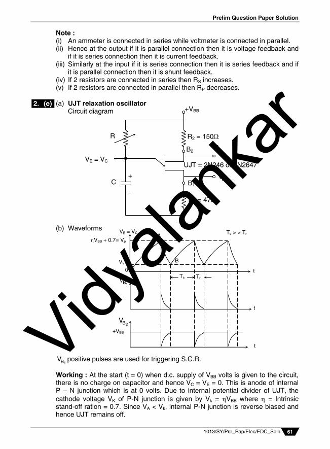
it is parallel connection then it is shunt feedback. (iv) If 2 resistors are connected in series then RS increases. (v) If 2 resistors are connected in parallel then RP decreases. (a) UJT relaxation oscillator Circuit diagram
(b) Waveforms
1BV positive pulses are used for triggering S.C.R.
Working : At the start (t = 0) when d.c. supply of VBB volts is given to the circuit, there is no charge on capacitor and hence VC = VE = 0. This is anode of internal P – N junction which is at 0 volts. Due to internal potential divider of UJT, the cathode voltage VK of P-N junction is given by Vk = VBB where = Intrinsic stand-off ration = 0.7. Since VA < Vk, internal P-N junction is reverse biased and hence UJT remains off.
2. (e)
B
A VBB + 0.7= Vp
Vv
0 t
t
t
1BV
2BV
+VBB
Tr Ts
Ts > > Tr VE = VC
+
C
R1 = 47
R2 = 150
B1
B2
+VBB
R
VE = VC
1BV
2BV
UJT = 2N246 or 2N2647
Vidyala
nkar
Vidyalankar : S.Y. Diploma EDC
1013/SY/Pre_Pap/Elec/EDC_Soln 62
OFF UJT acts like open switch and allows capacitor C to charge towards +VBB through variable resistor R. VC = VE now starts increasing exponentially and when VE = (VBB + 0.7) = VP then internal P-N junction is forward biased and starts conducting. UJT is now switched on and the charged capacitor starts discharging through ON UJT and resistor R1. VC = VE starts decreasing exponentially and when VE = Vv valley voltage, UJT goes automatically off.
OFF UJT once again acts like open switch and allows capacitor to charge. The entire waveform (O-A-B) respects itself thus producing continuous periodic sweep voltage oscillations.
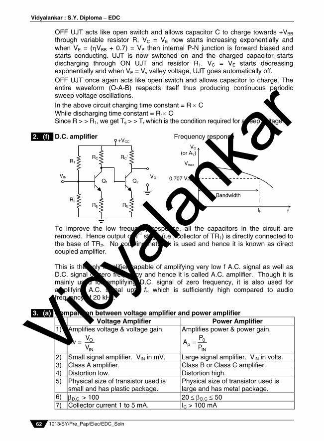
In the above circuit charging time constant = R C While discharging time constant = R1 C Since R > > R1, we get Ts > > Tr which is the condition required for sweep voltage. D.C. amplifier Frequency response To improve the low frequency response, all the capacitors in the circuit are removed. Hence output of 1st stage (i.e., collector of TR1) is directly connected to the base of TR2. No coupling network is used and hence it is known as direct coupled amplifier.
This is the only amplifier capable of amplifying very low f A.C. signal as well as D.C. signal of zero frequency and hence it is called A.C. amplifier. Though it is mainly used for amplifying D.C. signal of zero frequency, it is also used for amplifying A.C. signal upto fH which is sufficiently high compared to audio frequency of 20 kHz. Comparison between voltage amplifier and power amplifier
Voltage Amplifier Power Amplifier 1) Amplifies voltage & voltage gain.
Av = O
IN
VV
Amplifies power & power gain.
0p
IN
PA
P
2) Small signal amplifier. VIN in mV. Large signal amplifier. VIN in volts. 3) Class A amplifier. Class B or Class C amplifier. 4) Distortion low. Distortion high. 5) Physical size of transistor used is
small and has plastic package. Physical size of transistor used is large and has metal package.
6) D.C. > 100 20 D.C 50 7) Collector current 1 to 5 mA. IC > 100 mA
2. (f)
VIN
R1
R2
RE
RC
+VCC
RE
RC'
Q2 VO
Q1
f
VO
(or AV)
fH
0.707 Vmax
Vmax
Bandwidth
3. (a) Vidyala
nkar
Prelim Question Paper Solution
1013/SY/Pre_Pap/Elec/EDC_Soln 63
8) A.C. output power is low in mW. PAC > 1 watt 9) Output impedance is high 10 k to
12k Output impedance low 200
10) Normally RC coupled. Normally transformer coupled or direct coupled.
11) Heat sinks not required. Heat sinks must be used with power transistor.
12) Impedance matching poor. Excellent impedance matching. 13) Transistor used BC 147, 148, 547,
548. 549. Power transistor used SL100SK100, AC187AC188, 2N3055.
14) Transistors have thin base since it handles low current.
It has thick base to handle large current.
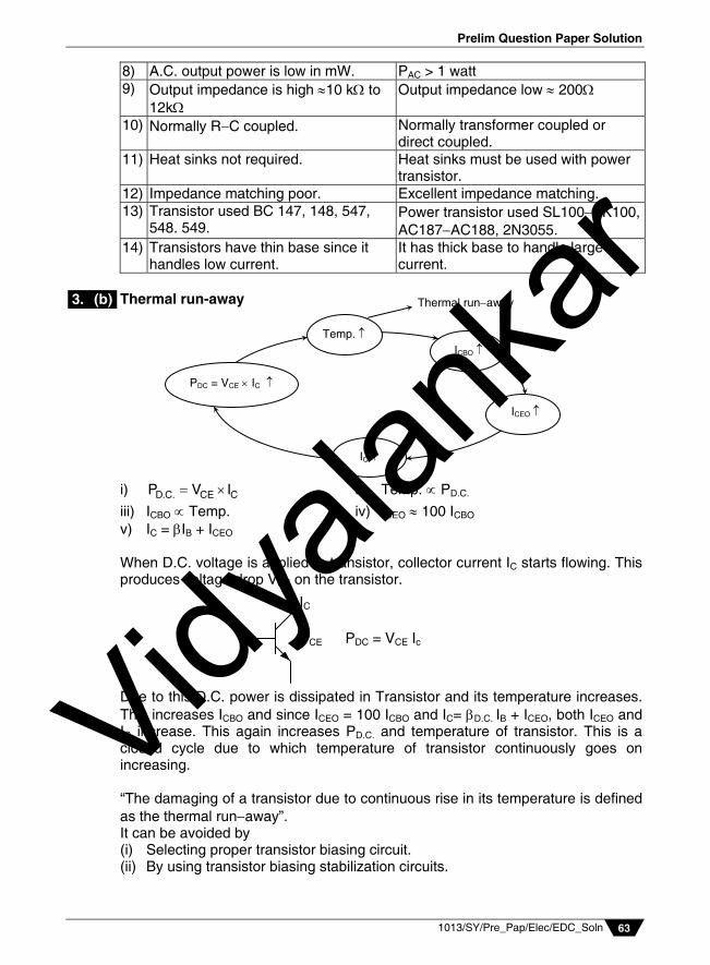
Thermal run-away
i) D.C. CE CP V I ii) Temp. PD.C.
iii) ICBO Temp. iv) ICEO 100 ICBO
v) IC = IB + ICEO
When D.C. voltage is applied to transistor, collector current IC starts flowing. This produces voltage drop VCE on the transistor.
Due to this D.C. power is dissipated in Transistor and its temperature increases. This increases ICBO and since ICEO = 100 ICBO and IC= D.C. IB + ICEO, both ICEO and IC increase. This again increases PD.C. and temperature of transistor. This is a closed cycle due to which temperature of transistor continuously goes on increasing. “The damaging of a transistor due to continuous rise in its temperature is defined as the thermal runaway”. It can be avoided by (i) Selecting proper transistor biasing circuit. (ii) By using transistor biasing stabilization circuits.
3. (b)
IC
VCE PDC = VCE Ic
Temp.
IC
ICEO
ICBO
PDC = VCE IC
Thermal runaway
Vidyala
nkar
Vidyalankar : S.Y. Diploma EDC
1013/SY/Pre_Pap/Elec/EDC_Soln 64
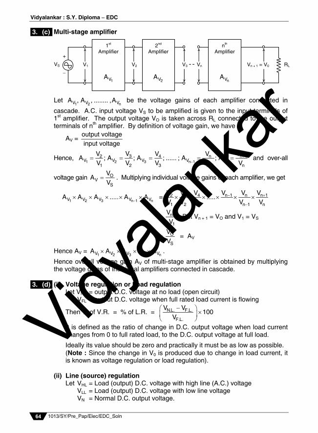
Multi-stage amplifier
Let 1 2 nV V VA , A , ........ ,A be the voltage gains of each amplifier connected in
cascade. A.C. input voltage VS to be amplified is given to the input terminals of 1st amplifier. The output voltage VO is taken across RL connected to the output terminals of nth amplifier. By definition of voltage gain, we have
AV = output voltageinput voltage
Hence, 1 2 3 n 1 n
32 4 n n 1V V V V V
1 2 3 n 1 n
VV V V VA ; A ; A ; ...... ; A ; A
V V V V V
and over-all
voltage gain OV
S
VA
V . Multiplying individual voltage gains of each amplifier, we get
1 2 3 n 1 nV V V V VA A A ..... A A
= 32 4 n 1 n n 1
1 2 3 n 1 n
VV V V V V.....
V V V V V
= n 1
1
VV But Vn + 1 = VO and V1 = VS
= O
S
VV
= AV
Hence AV = 1 2 3 nV V V VA A A ..... A .
Hence overall voltage gain AV of multi-stage amplifier is obtained by multiplying the voltage gains of individual amplifiers connected in cascade.
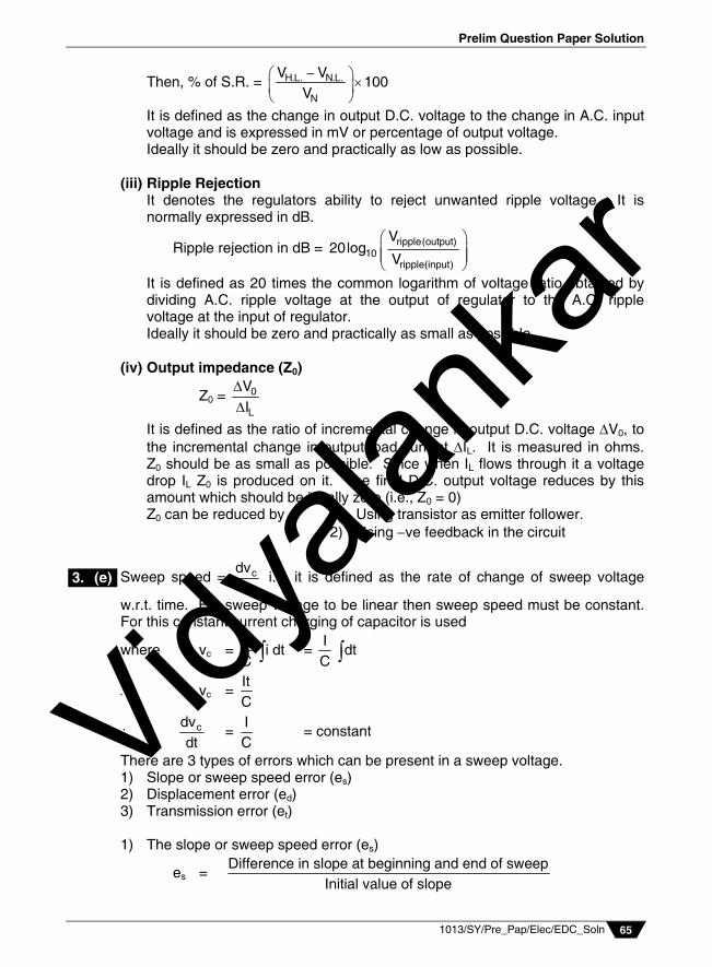
(i) Voltage regulation or Load regulation
Let VNL = output D.C. voltage at no load (open circuit) VFL = output D.C. voltage when full rated load current is flowing
Then % of V.R. = % of L.R. = N.L. F.L.
F.L.
V V100
V
It is defined as the ratio of change in D.C. output voltage when load current changes from 0 to full rated load, to the D.C. output voltage at full load.
Ideally its value should be zero and practically it must be as low as possible. (Note : Since the change in V0 is produced due to change in load current, it is known as voltage regulation or load regulation).
(ii) Line (source) regulation Let VHL = Load (output) D.C. voltage with high line (A.C.) voltage
VLL = Load (output) D.C. voltage with low line voltage VN = Normal D.C. output voltage.
3. (c)
V1
+
VS
1st Amplifier
1VA
V2
2nd Amplifier
2VA
V3 Vn
nth Amplifier
nVA
Vn + 1 = V0 RL
3. (d)
Vidyala
nkar
Prelim Question Paper Solution
1013/SY/Pre_Pap/Elec/EDC_Soln 65
Then, % of S.R. = H.L. N.L.
N
V V100
V
It is defined as the change in output D.C. voltage to the change in A.C. input voltage and is expressed in mV or percentage of output voltage.
Ideally it should be zero and practically as low as possible. (iii) Ripple Rejection
It denotes the regulators ability to reject unwanted ripple voltage. It is normally expressed in dB.
Ripple rejection in dB = ripple(output)10
ripple(input)
V20log
V
It is defined as 20 times the common logarithm of voltage ratio obtained by dividing A.C. ripple voltage at the output of regulator to the A.C. ripple voltage at the input of regulator. Ideally it should be zero and practically as small as possible.
(iv) Output impedance (Z0)
Z0 = 0
L
VI
It is defined as the ratio of incremental change in output D.C. voltage V0, to the incremental change in output load current IL. It is measured in ohms. Z0 should be as small as possible. Since when IL flows through it a voltage drop IL Z0 is produced on it. The final D.C. output voltage reduces by this amount which should be ideally zero (i.e., Z0 = 0)
Z0 can be reduced by 1) Using transistor as emitter follower. 2) Using ve feedback in the circuit
Sweep speed = cdvdt
i.e. it is defined as the rate of change of sweep voltage
w.r.t. time. For sweep voltage to be linear then sweep speed must be constant. For this constant current charging of capacitor is used
where vc = 1
i dtC =
Idt
C
vc = ItC
cdvdt
= IC
= constant
There are 3 types of errors which can be present in a sweep voltage. 1) Slope or sweep speed error (es) 2) Displacement error (ed) 3) Transmission error (et)
1) The slope or sweep speed error (es)
es = Difference in slope at beginning and end of sweep
Initial value of slope
3. (e)
Vidyala
nkar
Vidyalankar : S.Y. Diploma EDC
1013/SY/Pre_Pap/Elec/EDC_Soln 66
For ideal linear sweep, the slope remains same because it is a straight line and hence es = 0 for ideal sweep.
2) The displacement error (ed)
vs = Instantaneous value of actual sweep voltage
sv = Instantaneous value of linear sweep voltage
Vs = Maximum value of actual sweep voltage
Then ed = s s max
s
(v v )V
. Thus it is defined as the ratio of maximum
difference between the actual sweep voltage and the linear sweep voltage to the maximum value of actual sweep voltage.
3) The transmission error (et)
VS = Actual sweep voltage
sV = Linear sweep voltage
Normally RC coupling network is used at the output due to which transmission error is introduced.
Transmission error et = s s
s
V V
V
It is defined as the ratio of difference between uncompensated output and compensated output to the uncompensated output.
(a) By potential divider formula
Vf = 10
1 2
RV
R R
= 02
V2 8
Vf = 0.2 V0 …(1)
= 0.2 2 = 0.4 volts [V0 = 2V] Vf = 0.4 volts
Voltage
vs
TS t
s sV V
sv
VS
TS t
SV Without RC network
3. (f)
Vf +
V0
8k
2k R
Vin
+
Vf 2K
8mV A 2V RL = 1K
8K
Vidyala
nkar
Prelim Question Paper Solution
1013/SY/Pre_Pap/Elec/EDC_Soln 67
(b) From equation (1) Vf = 0.2 V0 But Vf = V0 Hence feedback factor = 0.2
(c) A = 0
id
VV
where V0 = 2 103 mV and Vid = 8 mV
Open loop gain, A =32 10
8
= 250 = A
(d) Afb = A
1 A =
2501 250 0.2
= 25051
= 4.902
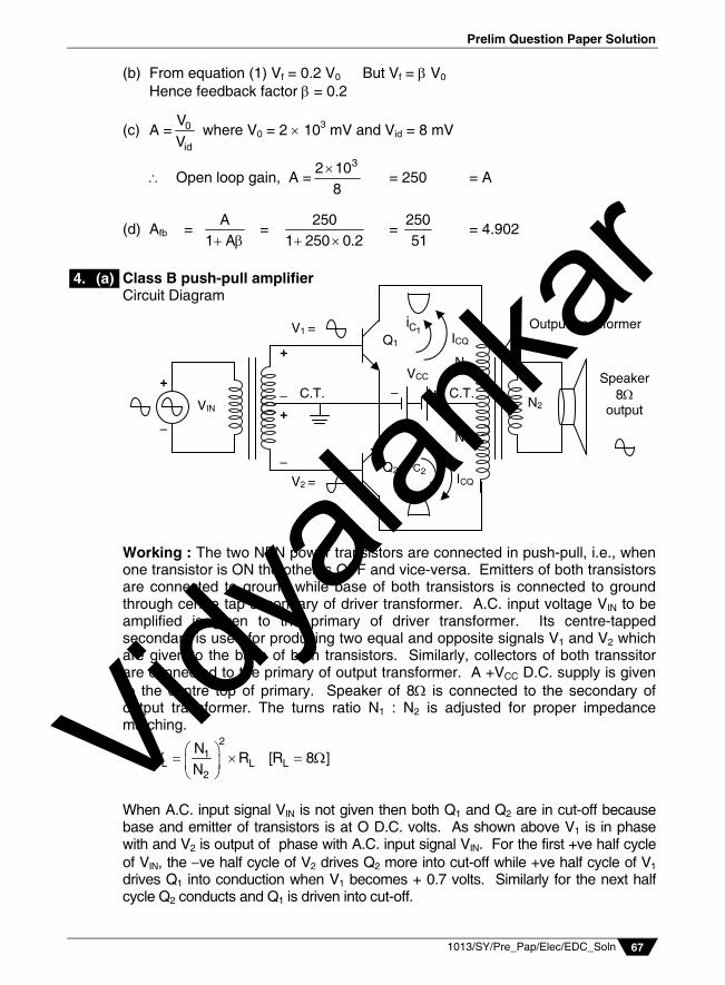
Class B push-pull amplifier Circuit Diagram
Working : The two NPN power transistors are connected in push-pull, i.e., when one transistor is ON the other is OFF and vice-versa. Emitters of both transistors are connected to ground while base of both transistors is connected to ground through centre tap secondary of driver transformer. A.C. input voltage VIN to be amplified is given to the primary of driver transformer. Its centre-tapped secondary is used for producing two equal and opposite signals V1 and V2 which are given to the base of both transistors. Similarly, collectors of both transsitor are connected to the primary of output transformer. A +VCC D.C. supply is given to the centre top of primary. Speaker of 8 is connected to the secondary of output transformer. The turns ratio N1 : N2 is adjusted for proper impedance matching.
2
1L L L
2
NR R [R 8 ]
N
When A.C. input signal VIN is not given then both Q1 and Q2 are in cut-off because base and emitter of transistors is at O D.C. volts. As shown above V1 is in phase with and V2 is output of phase with A.C. input signal VIN. For the first +ve half cycle of VIN, the ve half cycle of V2 drives Q2 more into cut-off while +ve half cycle of V1 drives Q1 into conduction when V1 becomes + 0.7 volts. Similarly for the next half cycle Q2 conducts and Q1 is driven into cut-off.
4. (a)
+
VIN
V1 =
V2 =
C.T.
+
+ Q1
Q2
N1
N1
N2
Speaker 8
output C.T. +
VCC
ICQ 2Ci
ICQ 1Ci Output transformer
Vidyala
nkar
Vidyalankar : S.Y. Diploma EDC
1013/SY/Pre_Pap/Elec/EDC_Soln 68
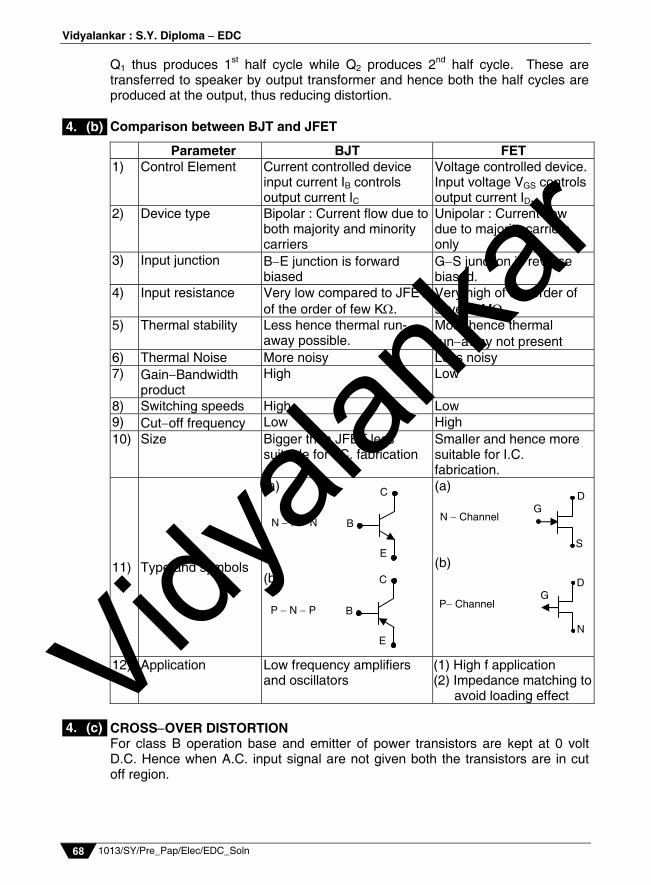
Q1 thus produces 1st half cycle while Q2 produces 2nd half cycle. These are transferred to speaker by output transformer and hence both the half cycles are produced at the output, thus reducing distortion. Comparison between BJT and JFET
Parameter BJT FET 1) Control Element Current controlled device
input current IB controls output current IC
Voltage controlled device. Input voltage VGS controls output current ID.
2) Device type Bipolar : Current flow due to both majority and minority carriers
Unipolar : Current flow due to majority carriers only
3) Input junction BE junction is forward biased
GS junction is reverse biased.
4) Input resistance Very low compared to JFET of the order of few K.
Very high of the order of several M.
5) Thermal stability Less hence thermal run-away possible.
More hence thermal runaway not present
6) Thermal Noise More noisy Less noisy 7) GainBandwidth
product High Low
8) Switching speeds High Low 9) Cutoff frequency Low High 10) Size Bigger than JFET less
suitable for I.C. fabrication Smaller and hence more suitable for I.C. fabrication.
11) Type and symbols
(a) (b)
(a) (b)
12) Application Low frequency amplifiers and oscillators
(1) High f application (2) Impedance matching to
avoid loading effect CROSSOVER DISTORTION For class B operation base and emitter of power transistors are kept at 0 volt D.C. Hence when A.C. input signal are not given both the transistors are in cut off region.
4. (b)
4. (c)
D
S
G N Channel
G D
N
P Channel
C
E
B N P N
C
E
B P N P
Vidyala
nkar
Prelim Question Paper Solution
1013/SY/Pre_Pap/Elec/EDC_Soln 69
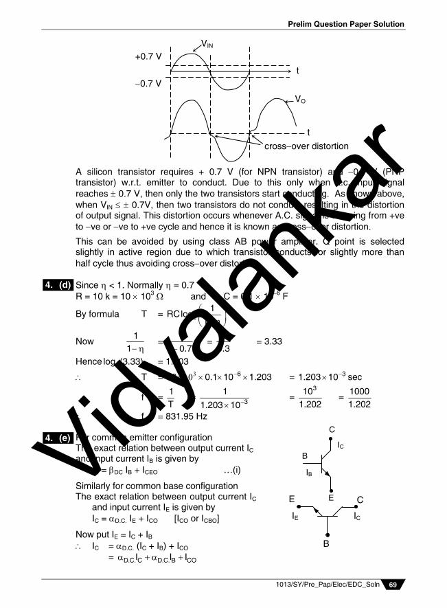
A silicon transistor requires + 0.7 V (for NPN transistor) and 0.7 V (PNP transistor) w.r.t. emitter to conduct. Due to this only when a.c. input signal reaches 0.7 V, then only the two transistors start conducting. As shown above, when VIN 0.7V, then two transistors do not conduct resulting in the distortion of output signal. This distortion occurs whenever A.C. signal is crossing from +ve to ve or ve to +ve cycle and hence it is known as crossover distortion.
This can be avoided by using class AB power amplifier. Q point is selected slightly in active region due to which transistor conducts for slightly more than half cycle thus avoiding crossover distortion. Since < 1. Normally = 0.7
R = 10 k = 10 103 and C = 0.1 106 F
By formula T = e1
RClog1
Now 1
1 =
11 0.7
= 1
0.3 = 3.33
Hence elog (3.33) = 1.203
T = 610 0.1 10 1.203 = 31.203 10 sec
f = 1T
= 3
1
1.203 10 =
3101.202
= 10001.202
f = 831.95 Hz For common emitter configuration The exact relation between output current IC and input current IB is given by IC = DC IB + ICEO …(i)
Similarly for common base configuration The exact relation between output current IC
and input current IE is given by IC = D.C. IE + ICO [ICO or ICBO]
Now put IE = IC + IB IC = D.C. (IC + IB) + ICO
= D.C. C D.C. B COI I I
4. (d)
4. (e)
VIN
VO
t
crossover distortion
+0.7 V
0.7 V t
IC
IB
C
E
B
C E
B
IC IE
Vidyala
nkar
Vidyalankar : S.Y. Diploma EDC
1013/SY/Pre_Pap/Elec/EDC_Soln 70
Fig. 1 : RC phase shift oscillator using transistor
C D.C. C D.C. B COI I I I
D.C. C D.C. B CO(1 )I I I
COC B
II I
1 1
…(ii)
Companies equations (i) & (ii) we get
= 1
and CEO1
I1
ICO
Now by formula = 1
CEO1
I1
1
ICO = CO CO1
I 1 I1
1
But normally 100 < < 500. Also neglecting 1 we can write + 1 100 ICEO = 100 ICO
Hence reverse leakage current in common emitter is 100 times greater than the reverse leakage current in common base configuration.
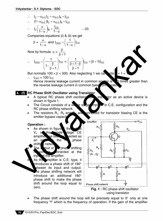
RC Phase Shift Oscillator using Transistor A typical RC phase shift oscillator using transistor as an active device is
shown in figure 1. The Circuit consists of a single stage amplifier in C.E. configuration and the
RC phase shifting network. The resistors R1, R2 and RE are connected for transistor biasing CE is the
emitter bypass capacitor. Operation : As shown in figure 1 the output
Vo of the single stage CE amplifier has been connected as an input to the RC phase shifting network.
The output of the phase shifting network is connected at the input of the amplifier.
As the amplifier is C.E. type, it introduces a phase shift of 180 between its input and output. The phase shifting network will introduce an additional 180 phase shift to make the phase shift around the loop equal to zero.
The phase shift around the loop will be precisely equal to 0 only at one frequency "f" which is the frequency of operation. If the gain of the amplifier
4. (f)
Vidyala
nkar
Prelim Question Paper Solution
1013/SY/Pre_Pap/Elec/EDC_Soln 71
and feedback factor are adjusted properly to have a loop gain |A| 1 the sustained sinusoidal oscillations will be obtained at the oscillator output.
Note that the RC feedback network of figure 1 is slightly different from the one we have discussed in section 6. The resistance R3 of Figure 1 is selected in such a way that,
R3 + Zi = R ... (1) where, Zi = Input impedance of the CE amplifier. It is given by, Zi = hie || (R1 || R2)
But as R1 and R2 are large enough. We can neglect them. Hence, Zi hie
Substituting this value into Equation (1) we get, R3 + hie = R or R3 = R hie ... (2)
And if we do not neglect the resistors R1 and R2 then the value of R3 is given by, R3 = R [R1 || R2 || hie] ... (3)
Av = open loop voltage gain; Afb = Closed loop voltage gain;
= feedback factor then by formula Afb = v
v
A1 A
Now 1 i.e. normally is always less than 1 and its maximum value can be only one. But the open loop voltage gain Av is very high and hence Av >> 1. Neglecting 1 in the denominator we get
Afb = v
v
AA
=1
Thus closed loop gain Afb is equal to the reciprocal of feedback factor . In ve feedback amplifiers only resistors are used whose values are fixed once
they are selected. = Ratio of these resistors 1
1 f
RR R
which is constant.
Thus Afb remains constant and is independent of the parameter of the transistor (a.c or hfe). Because of this reason, stability of voltage amplifier improves when ve feedback is used.
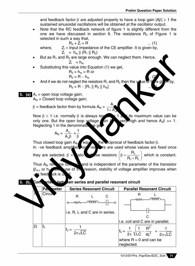
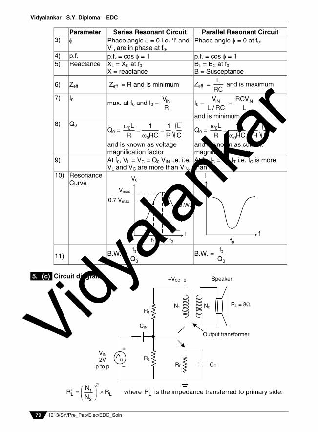
Comparison between series and parallel resonant circuit
Parameter Series Resonant Circuit Parallel Resonant Circuit 1) Circuit
i.e. R, L and C are in series.
i.e. coil and C are in parallel.
2) f0 f0 =
1
2 LC f0 =
2
2
1 1 R2 LC 4L
1
2 LC
where R 0 and can be neglected.
5. (a)
5. (b)
R L C R L
C Vidyala
nkar
Vidyalankar : S.Y. Diploma EDC
1013/SY/Pre_Pap/Elec/EDC_Soln 72
Parameter Series Resonant Circuit Parallel Resonant Circuit 3) Phase angle = 0 i.e. ‘I’ and
Vin are in phase at f0. Phase angle = 0 at f0.
4) p.f. p.f. = cos = 1 p.f. = cos = 1 5) Reactance XL = XC at f0
X = reactance BL = BC at f0 B = Susceptance
6) Zeff Zeff = R and is minimum Zeff = L
RC and is maximum
7) I0 max. at f0 and I0 = INV
R I0 = INV
L / RC = INRCV
L
and is minimum 8) Q0
Q0 = 0
0
L 1 1 LR RC R C
and is known as voltage magnification factor
Q0 = 0
0
L 1 1 LR RC R C
and is known as current magnification factor.
9) At f0, VL = VC = Q0 VIN i.e. i.e. VL and VC are more than VIN.
At f0, IC = Q0 IT i.e. IC is more than IT.
10) Resonance Curve
11)
B.W. = 0
0
fQ
B.W. = 0
0
fQ
Circuit diagram :
21
L L2
NR R
N
where LR is the impedance transferred to primary side.
5. (c)
V0
f f1 f0 f2
Vmax
0.7 Vmax B.W.
I
f f0
+
R2
R1
RE
VIN 2V
p to p
N1 N2
+VCC Speaker
RL = 8
Output transformer
CE
CIN Vidyala
nkar
Prelim Question Paper Solution
1013/SY/Pre_Pap/Elec/EDC_Soln 73
Working : The resistors R1 and R2 are voltage divider biasing network which establishes Q point in the centre of a active region. RE stabilizes the Q point. By-pass capacitor CE by-passes A.C. output signal from the emitter. This removes ve feedback which improves the gain of the amplifier. Input capacitor CIN blocks D.C. voltage and allows A.C. input voltage VIN to pass to the base of transistor. The collector resistor RC is replaced by the primary winding of output transformer. Its resistance is very small which reduces power losses in it thus improving power efficiency. The maximum improves from 25% (for RC) to 50% (for transformer coupled). The transformer gives good D.C. isolation as well as impedance matching. Speaker impedance of 8 (RL) on secondary side is transferred to LR on primary
side, where2
1L L
2
NR R
N
. Hence by using step-down (N2 < N1) transformers,
impedance of speaker is matched to the output impedance of amplifier. Due to this maximum power is transferred to the loud-speaker. Advantages :
(i) Bandwidth of the amplifier increases (B.W.)new = (1 + Av)(B.W.)old (ii) (Amplitude, frequency, phase harmonic) distortion of the amplifier reduces.
D0 (new) = old
v
D(1 A )
(iii) Noise signal in the output reduces.
0(old)0(new)
v
NN
1 A
(iv) Stability of the amplifier improves due to which voltage gain becomes independent of transistor parameters and hence it remains almost constant.
(v) (a) RIN for voltage amplifier should be high. (b) R0 of voltage amplifier should be low.
By using voltage series ve feedback amplifier, RIN increases and R0 decreases.
(new)INR = (1 + Av) RIN(old)
RO(new) = 0(old)
v
R
1 A
Disadvantages :
The only disadvantage is that voltage gain of the amplifier decreases
Afb = v
v
A1 A
But if more voltage gain is required then multistage amplifiers with ve feedback can be used.
5. (d)
Vidyala
nkar
Vidyalankar : S.Y. Diploma EDC
1013/SY/Pre_Pap/Elec/EDC_Soln 74
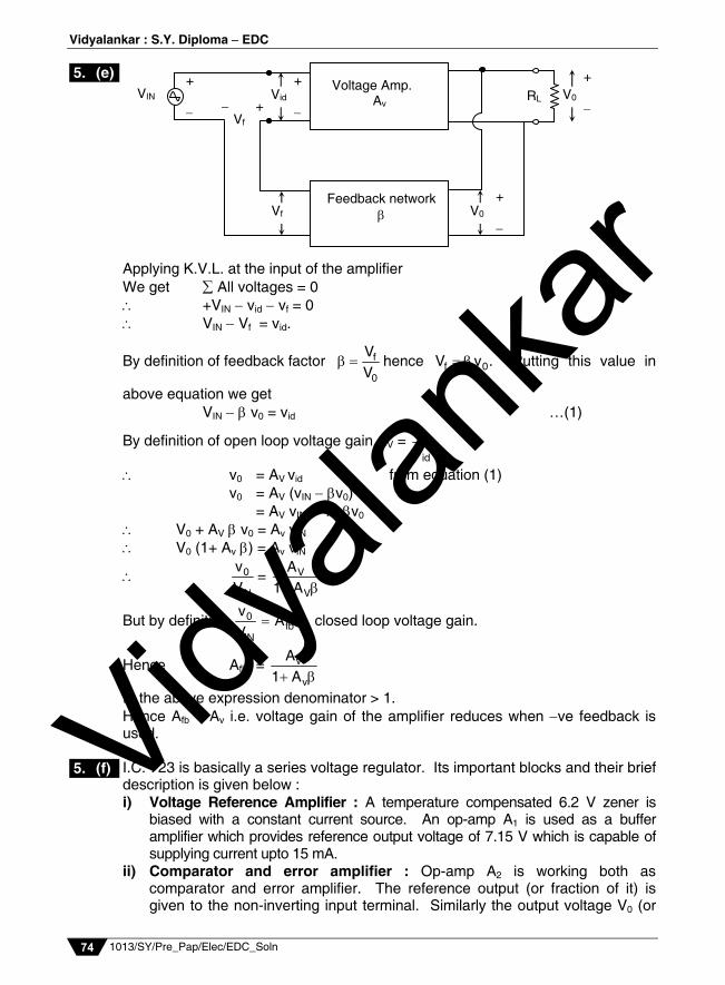
Applying K.V.L. at the input of the amplifier We get All voltages = 0 +VIN vid vf = 0 VIN Vf = vid.
By definition of feedback factor f
0
VV
hence f 0V v . Putting this value in
above equation we get VIN v0 = vid …(1)
By definition of open loop voltage gain AV = 0
id
vv
v0 = AV vid from equation (1) v0 = AV (vIN v0) = AV vIN AVv0 V0 + AV v0 = Av vIN V0 (1+ Av ) = Av vIN
0
IN
vV
= V
V
A1 A
But by definition 0fb
IN
vA
V closed loop voltage gain.
Hence Afb = v
v
A1 A
In the above expression denominator > 1. Hence Afb < Av i.e. voltage gain of the amplifier reduces when ve feedback is used. I.C. 723 is basically a series voltage regulator. Its important blocks and their brief description is given below : i) Voltage Reference Amplifier : A temperature compensated 6.2 V zener is
biased with a constant current source. An op-amp A1 is used as a buffer amplifier which provides reference output voltage of 7.15 V which is capable of supplying current upto 15 mA.
ii) Comparator and error amplifier : Op-amp A2 is working both as comparator and error amplifier. The reference output (or fraction of it) is given to the non-inverting input terminal. Similarly the output voltage V0 (or
5. (e)
5. (f)
Voltage Amp. Av
Feedback network
+
+
VIN +
Vid V0
Vf V0 +
RL +
Vf
Vidyala
nkar
Prelim Question Paper Solution
1013/SY/Pre_Pap/Elec/EDC_Soln 75
fraction of it) is given to the inverting input terminal of op-amp A2. These two voltages are compared with each other and the difference between them known as error voltage is produced. This error voltage is amplified by op-amp A2 and is available at its output as control voltage.
iii) Output Stage : It consists of series pass control transistor Q2. The control
voltage at the output of op-amp. A2 is given to the base of Q2. This control voltage adjusts the voltage drop VCE of Q2 till error voltage becomes zero and V0 remains constant.
iv) Over-Current protection circuit : Transistor Q1 connected at the output works as current protection circuit. An external resistor RCL connected between its base (current limit) and emitter (current sense) fixes the maximum value of the load current. Under short circuit condition also the load current does not exceed this value.
v) How to vary the output voltage : A potentiometer R2 is varied to change the output voltage to the required value. This R2 is connected in potential divider circuit across output terminals or it is connected to reference output terminal.
Zener Diode in Parallel to RL
Circuit Diagram :
Equations : (i) V0 = VZ hence if VZ is constant then V0 is constant. (ii) By K.C.L. at A , IT = IZ + IL (iii) By K.V.L., All voltages = 0 IN T S 0V I R V 0
6. (a)
+
A2
Q1
Q2
VZ
V0
VC
C.S. (Current sense)
C.L. (Current
limit)
Frequency compensation
A1
I Constant current source
Temperature Compensated zener
A1 : voltage reference amplifier
Vref.
Inverting input
Non-inverting input
A2 : Comparator and Error Amplifier
Booster terminal
Current protection circuit
Output Stage
V+
V
RS
IT
VZ = V0 RL
IL
IZ
A
VIN Vidyala
nkar
Vidyalankar : S.Y. Diploma EDC
1013/SY/Pre_Pap/Elec/EDC_Soln 76
V0 = VZ = VIN IT RS and ITRS = VIN VZ
RS = IN Z
T
V VI
= IN Z
Z L
V VI I
(iv) Thus by selecting the value of RS properly the condition (knee) (max)Z Z ZI I I is
satisfied for all conditions due to which VZ = V0 remains constant. Working : VIN varying IL constant : It is assumed that RS is so selected that V0 = VZ = constant.
A B 1. Assume VIN increases. Assume VIN decreases. 2. This increases VIN V0 This decreases VIN V0 3. IT increases and IT = IZ + IL. But IL is
constant since V0 is constant IT decreases and IT = IZ + IL. But IL is constant since V0 is constant.
4. IZ increases but IZ < max.ZI hence V0 is
constant
IZ decreases but IZ > (knee)ZI hence V0
is constant. Conditions necessary for this circuit to work properly are
(i) VIN > VZ, so that zener diode is properly reverse biased. (ii) Value of RS is so selected that under all conditions;
(knee) (max.)Z Z ZI I I is
satisfied. Hence zener diode operates in proper breakdown condition and VZ = V0 remains constant.
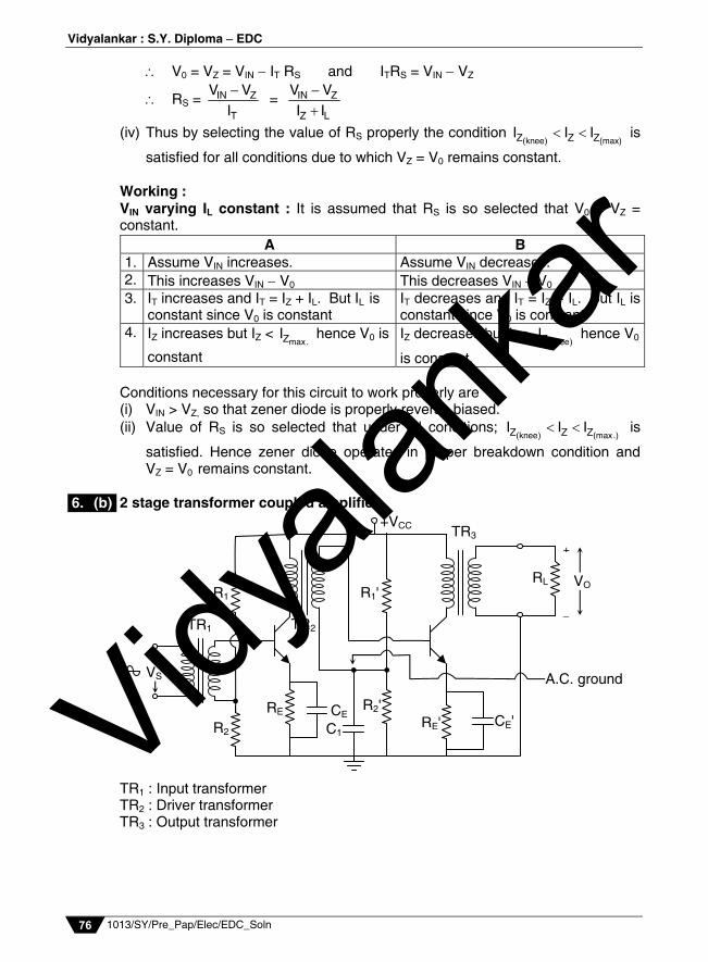
2 stage transformer coupled amplifier
TR1 : Input transformer TR2 : Driver transformer TR3 : Output transformer
6. (b) +VCC
+
RE' CE'
VO
VS
TR1
R1
R2
RE CE
R1'
R2'
RL
TR3
TR2
A.C. ground
C1Vidyala
nkar
Prelim Question Paper Solution
1013/SY/Pre_Pap/Elec/EDC_Soln 77
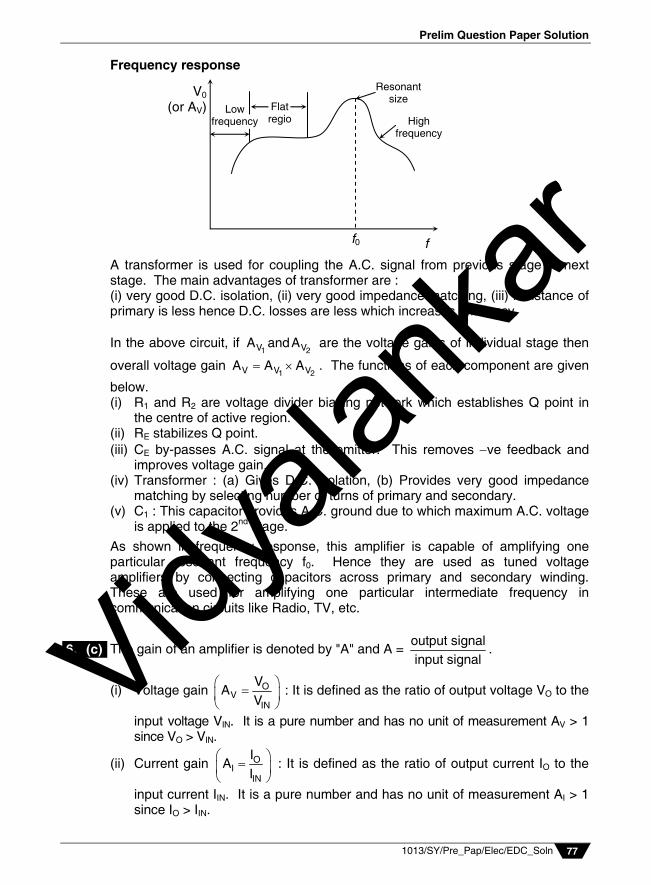
Frequency response
A transformer is used for coupling the A.C. signal from previous stage to next stage. The main advantages of transformer are : (i) very good D.C. isolation, (ii) very good impedance matching, (iii) resistance of primary is less hence D.C. losses are less which increases efficiency.
In the above circuit, if
1 2V VA andA are the voltage gains of individual stage then
overall voltage gain 1 2V V VA A A . The functions of each component are given
below. (i) R1 and R2 are voltage divider biasing network which establishes Q point in
the centre of active region. (ii) RE stabilizes Q point. (iii) CE by-passes A.C. signal at the emitter. This removes ve feedback and
improves voltage gain. (iv) Transformer : (a) Gives D.C. isolation, (b) Provides very good impedance
matching by selecting number of turns of primary and secondary. (v) C1 : This capacitor provides A.C. ground due to which maximum A.C. voltage
is applied to the 2nd stage.
As shown in frequency response, this amplifier is capable of amplifying one particular resonant frequency f0. Hence they are used as tuned voltage amplifiers by connecting capacitors across primary and secondary winding. These are used for amplifying one particular intermediate frequency in communication circuits like Radio, TV, etc.
The gain of an amplifier is denoted by "A" and A = output signalinput signal
.
(i) Voltage gain OV
IN
VA
V
: It is defined as the ratio of output voltage VO to the
input voltage VIN. It is a pure number and has no unit of measurement AV > 1 since VO > VIN.
(ii) Current gain OI
IN
IA
I
: It is defined as the ratio of output current IO to the
input current IIN. It is a pure number and has no unit of measurement AI > 1 since IO > IIN.
6. (c)
f f0
V0
(or AV) Low frequency
Flat regio
Resonant size
High frequency
Vidyala
nkar
Vidyalankar : S.Y. Diploma EDC
1013/SY/Pre_Pap/Elec/EDC_Soln 78
(iii) Power gain OP
in
PA
P
: It is defined as the ratio of output power PO to the
input power PIN. It is a pure number and it has no unit of measurement. Relation between AV, AI and AP Multiplying the values of AV and AI, we get
AV AI = O O
IN IN
V IV I
= O O
IN IN
V IV I
= O
IN
PP
= AP
Since VO IO = output power PO and VIN IIN = input power Thus AP = AV AI
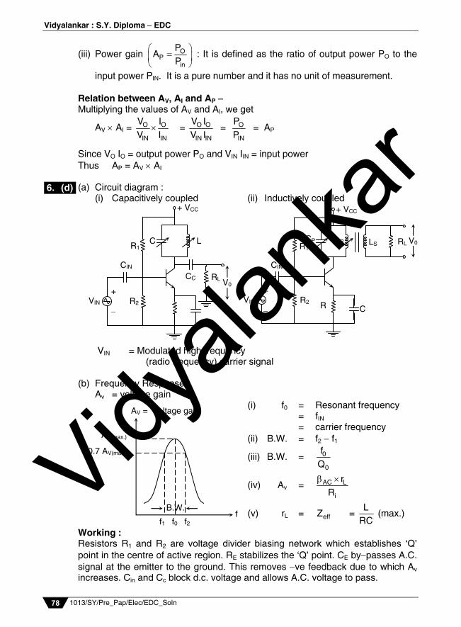
(a) Circuit diagram :
(i) Capacitively coupled (ii) Inductively coupled VIN = Modulated high frequency (radio frequency) carrier signal (b) Frequency Response : Av = voltage gain (i) f0 = Resonant frequency = fIN
= carrier frequency (ii) B.W. = f2 f1
(iii) B.W. = 0
0
fQ
(iv) Av = AC L
i
rR
(v) rL = effZ = L
RC (max.)
Working : Resistors R1 and R2 are voltage divider biasing network which establishes ‘Q’ point in the centre of active region. RE stabilizes the ‘Q’ point. CE bypasses A.C. signal at the emitter to the ground. This removes ve feedback due to which Av increases. Cin and Cc block d.c. voltage and allows A.C. voltage to pass.
6. (d)
+
R1
R2
V0 CC
VIN
+ VCC
CIN RL
C L
+
R1
R2
V0
VIN
+ VCC
CIN
CP
R C
LP LS RL
AV = Voltage gain
f f1 f0 f2
AV(max.)
0.7 AV(max.)
B.W. Vidyala
nkar
Prelim Question Paper Solution
1013/SY/Pre_Pap/Elec/EDC_Soln 79
In the above circuit Rc is replaced by single tuned (parallel resonant) circuit. Either L or C or both are variable. Their values are so adjusted (tuned) that resonant
frequency 01
f2 LC
of the tuned circuit becomes exactly equal to incoming
signal frequency. At f0, Zeff of parallel circuit becomes maximum and is given by
Zeff = L
RCwhere R = resistance of inductor. As shown above Av Zeff and hence
voltage gain becomes maximum at f0 as shown in the frequency response.
B.W. = 0
0
fQ
and hence as Q0 increases, frequency response becomes more
narrower and bandwidth decreases. Hence circuit becomes more selective.
Thus the circuit is capable of amplifying one particular high frequency (f0) or a very narrow band of high frequencies (f2 f1). Since only 1 tuned circuit is used. It is known as singletuned voltage amplifier. The output voltage can be either capacitively coupled or inductively coupled. Advantages : (i) Maximum power, = 78.4% which is higher than Class A amplifier.
(ii) Even harmonic components are eliminated.
(iii) More A.C. power output per transistor than Class A.
(iv) D.C. current of both transistor flow in opposite direction in the primary winding of output transformer. Hence magnetic fluxes produced by them cancel each other due to which core of transformer does not saturate.
(v) It is possible to eliminate both the transformers which reduces the cost and improves the frequency response.
Disadvantages : (i) Two power transistors are required when increases the cost.
(ii) The two transistors must be a matched pair, i.e., their parameters must be identical to avoid distortion. This also increases the cost of power transistor.
(iii) Driver stage required for producing two equal and opposite A.C. input signals.
(iv) Distortion is more than Class A amplifier.
(v) Because of Class B operation, cross-over distortion present.
(vi) Transformers are bulky and occupy more space.
(vii) Cost increases because of 2 transformers.
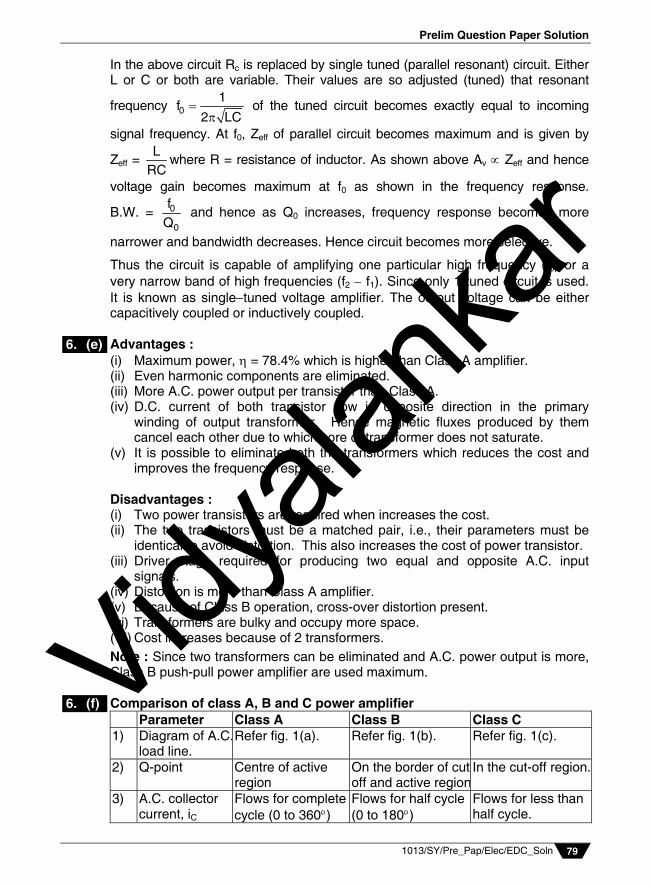
Note : Since two transformers can be eliminated and A.C. power output is more, Class B push-pull power amplifier are used maximum. Comparison of class A, B and C power amplifier Parameter Class A Class B Class C 1) Diagram of A.C.
load line. Refer fig. 1(a). Refer fig. 1(b). Refer fig. 1(c).
2) Q-point Centre of active region
On the border of cutoff and active region
In the cut-off region.
3) A.C. collector current, iC
Flows for complete cycle (0 to 360)
Flows for half cycle (0 to 180)
Flows for less than half cycle.
6. (e)
6. (f) Vidyala
nkar
Vidyalankar : S.Y. Diploma EDC
1013/SY/Pre_Pap/Elec/EDC_Soln 80
4) D.C. collector current, IC
Flows even if A.C. input signal is not given.
Does not flow if A.C.input signal absent.
Does not flow if A.C.input signal absent.
5) Maximum power,
25% for RC 50% for TX (Lowest)
78.4% (Medium)
> 80% (Highest)
6) Distortion Lowest Medium Highest 7) Output power to
load. Lowest High Highest
8) Cross-over distortion
Not present Present Not present
9) Hum (Noise signal)
Absent Low High
Vidyala
nkar


![B.E. Sem. VII [EXTC] Fundamentals of Microwave …vidyalankar.org/file/engg_degree/prelim_paper_soln/SemVII/EXTC/... · Fundamentals of Microwave Engineering Prelim Question Paper](https://img.pdfslide.us/doc/110x75/5ab168727f8b9ad9788c3916/be-sem-vii-extc-fundamentals-of-microwave-of-microwave-engineering-prelim.jpg)