Embed Size (px)
Citation preview

PH
VIN
POWERPAD
BOOT
VSENSE
COMP
TPS54519
EN
RT
SS/TR
PWRGD
Css
RT R3
C1
CBOOT
CO
LO
R1
R2
CI
VOUT
VIN
AGND
GND
R4
R5
50
60
70
80
90
100
0 0.5 1 1.5 2 2.5 3 3.5 4 4.5 5
Eff
icie
ncy -
%
V = 1.2 V
F
OUT
SW= 1MHz
V = 5 VIN
I - Load Current - AL
V = 3 VIN
TPS54519
www.ti.com SLVSAT3A –SEPTEMBER 2011–REVISED DECEMBER 2013
2.95 V to 6 V Input, 5-A Synchronous Step Down SWIFT™ Converter1FEATURES DESCRIPTION
The TPS54519 device is a full featured 6 V, 5 A,2• Two 30 mΩ (typical) MOSFETs for high
synchronous step down current mode converter withefficiency at 5-A loadstwo integrated MOSFETs.
• 200kHz to 2MHz Switching FrequencyThe TPS54519 enables small designs by integrating• 0.6 V Voltage Reference With ± 1% Initial the MOSFETs, implementing current mode control toAccuracy reduce external component count, reducing inductor
• Adjustable Slow Start / Sequencing size by enabling up to 2 MHz switching frequency,and minimizing the IC footprint with a small 3mm x• UV and OV Power Good Output3mm thermally enhanced QFN package.• Low Operating and Shutdown Quiescent
Current Efficiency is maximized through the integrated 30mΩMOSFETs and 350μA typical supply current. Using• Safe Start-up into Pre-Biased Outputthe enable pin, shutdown supply current is reduced to• Cycle by Cycle Current Limit, Thermal and 2 μA by entering a shutdown mode.
Frequency Fold Back ProtectionUnder voltage lockout is internally set at 2.6 V, but• –40°C to 140°C Operating Junction can be increased by programming the threshold withTemperature Range a resistor network on the enable pin. The output
• Thermally Enhanced 3mm × 3mm 16-pin QFN voltage startup ramp is controlled by the slow startpin. An open drain power good signal indicates theoutput is within 93% to 107% of its nominal voltage.APPLICATIONS
• Low-Voltage, High-Density Power Systems Frequency fold back and thermal shutdown protectsthe device during an overcurrent condition.• Point of Load Regulation for High Performance
DSPs, FPGAs, ASICs and Microprocessors The TPS54519 is supported in the SwitcherPro™Software Tool at www.ti.com/switcherpro.• Broadband, Networking and Optical
Communications Infrastructure For more SWIFT™ documentation, see the TIwebsite at www.ti.com/swift.
SIMPLIFIED SCHEMATIC
1
Please be aware that an important notice concerning availability, standard warranty, and use in critical applications ofTexas Instruments semiconductor products and disclaimers thereto appears at the end of this data sheet.
2SWIFT, SwitcherPro are trademarks of Texas Instruments.PRODUCTION DATA information is current as of publication date. Copyright © 2011–2013, Texas Instruments IncorporatedProducts conform to specifications per the terms of the TexasInstruments standard warranty. Production processing does notnecessarily include testing of all parameters.

TPS54519
SLVSAT3A –SEPTEMBER 2011–REVISED DECEMBER 2013 www.ti.com
This integrated circuit can be damaged by ESD. Texas Instruments recommends that all integrated circuits be handled withappropriate precautions. Failure to observe proper handling and installation procedures can cause damage.
ESD damage can range from subtle performance degradation to complete device failure. Precision integrated circuits may be moresusceptible to damage because very small parametric changes could cause the device not to meet its published specifications.
ORDERING INFORMATIONTJ PACKAGE PART NUMBER
–40°C to 140°C 3 × 3 mm QFN TPS54519RTE
ABSOLUTE MAXIMUM RATINGSVALUE UNIT
MIN MAXInput voltage VIN –0.3 7 V
EN –0.3 7BOOT PH + 8VSENSE –0.3 3COMP –0.3 3PWRGD –0.3 7SS/TR –0.3 3RT –0.3 6
Output voltage BOOT-PH 8 VPH –0.6 7PH 10 ns Transient –2 7
Source current EN 100 μART 100
Sink current COMP 100 μAPWRGD 10 mASS/TR 100 μA
Electrostatic discharge (HBM) 2 kVElectrostatic discharge (CDM) 500 VOperating Junction temperature, Tj –40 140 °CStorage temperature, Tstg –65 150 °C
THERMAL INFORMATIONTPS54519
THERMAL METRIC (1) (2) UNITSRTE (16 PINS)
θJA Junction-to-ambient thermal resistance (standard board) 49.1θJA Junction-to-ambient thermal resistance (custom board) (3) 37.0ψJT Junction-to-top characterization parameter 0.7ψJB Junction-to-board characterization parameter 21.8 °C/WθJC(top) Junction-to-case(top) thermal resistance 50.7θJC(bot) Junction-to-case(bottom) thermal resistance 7.5θJB Junction-to-board thermal resistance 21.8
(1) For more information about traditional and new thermal metrics, see the IC Package Thermal Metrics application report, SPRA953.(2) Power rating at a specific ambient temperature TA should be determined with a junction temperature of 140°C. This is the point where
distortion starts to substantially increase. See power dissipation estimate in the application section of this data sheet for moreinformation.
(3) Test boards conditions:(a) 2 inches x 2 inches, 4 layers, thickness: 0.062 inch(b) 2 oz. copper traces located on the top of the PCB(c) 2 oz. copper ground planes on the 2 internal layers and bottom layer(d) 4 thermal vias (10mil) located under the device package
2 Submit Documentation Feedback Copyright © 2011–2013, Texas Instruments Incorporated
Product Folder Links: TPS54519

TPS54519
www.ti.com SLVSAT3A –SEPTEMBER 2011–REVISED DECEMBER 2013
ELECTRICAL CHARACTERISTICSTJ = –40°C to 140°C, VIN = 2.95 to 6 V (unless otherwise noted)
DESCRIPTION CONDITIONS MIN TYP MAX UNITSUPPLY VOLTAGE (VIN PIN)Operating input voltage 2.95 6 VInternal under voltage lockout threshold No voltage hysteresis, rising and falling 2.4 2.8 VShutdown supply current EN = 0 V, 25°C, 2.95 V ≤ VIN ≤ 6 V 1 5 μAQuiescent Current - Iq VSENSE = 0.9 V, 25°C, RT = 400 kΩ 455 500 μAENABLE AND UVLO (EN PIN)
Rising 1.16 1.25 1.37 VEnable threshold
Falling 1.18Enable threshold + 50 mV -3.6
Input current μAEnable threshold – 50 mV -0.7
VOLTAGE REFERENCE (VSENSE PIN)Voltage Reference 0 A ≤ IOUT ≤ 5 A, 25°C 0.594 0.600 0.606 VMOSFET
BOOT-PH= 5 V 30 60High side switch resistance mΩ
BOOT-PH= 2.95 V 35 70VIN= 5 V 30 60
Low side switch resistance mΩVIN= 2.95 V 35 70
ERROR AMPLIFIERInput current 50 nAError amplifier transconductance (gm) –2 μA < I(COMP) < 2 μA, V(COMP) = 1 V 250 μmhosError amplifier transconductance (gm) during –2 μA < I(COMP) < 2 μA, V(COMP) = 1 V, 85 μmhosslow start Vsense = 0.4 VError amplifier source/sink V(COMP) = 1 V, 100 mV overdrive ±20 μACOMP to Iswitch gm 19.0 A/VCURRENT LIMITCurrent limit threshold 6.0 7.0 8.0 ALow-side reverse current limit –2.7 ATHERMAL SHUTDOWNThermal Shutdown 150 155 °CHysteresis 7.5 °CTIMING RESISTOR (RT PIN)Switching frequency range using RT mode 200 2000 kHzSwitching frequency Rt = 84 kΩ 400 490 600 kHzPH (PH PIN)
Measured at 50% points on PH, VIN = 5 V, IOUT = 100 nsMinimum On time 500 mAPrior to skipping off pulses, BOOT-PH = 2.95 V, 60 nsMinimum Off time IOUT = 4 A
Rise/Fall Time VIN = 5 V 1.5 V/ns
Copyright © 2011–2013, Texas Instruments Incorporated Submit Documentation Feedback 3
Product Folder Links: TPS54519

TPS54519
SLVSAT3A –SEPTEMBER 2011–REVISED DECEMBER 2013 www.ti.com
ELECTRICAL CHARACTERISTICS (continued)TJ = –40°C to 140°C, VIN = 2.95 to 6 V (unless otherwise noted)
DESCRIPTION CONDITIONS MIN TYP MAX UNITBOOT (BOOT PIN)BOOT Charge Resistance VIN = 5 V 15 ΩBOOT-PH UVLO VIN = 2.95 V 2.1 2.75 VSLOW START / TRACKING (SS/TR PIN)Charge Current V(SS) = 0.3 V 2.4 μASS/TR to VSENSE matching VSSTR = 0.3 V 73 115 mVSS to reference crossover 98% nominal 0.87 VSS discharge voltage (overload) VSENSE = 0 V 80 μASS discharge current (UVLO, EN, Thermal VIN = 5 V, V(SS) = 0.5 V 1.2 mAFault)POWER GOOD (PWRGD PIN)
VSENSE rising (Good) 93 % VrefVSENSE threshold
VSENSE rising (Fault) 110 % VrefHysteresis VSENSE falling 2 % VrefOutput high leakage VSENSE = VREF, V(PWRGD) = 5.5 V 100 nAOn resistance 78 ΩOutput low I(PWRGD) = 3.5 mA 0.5 VMinimum VIN for valid output V(PWRGD) < 0.5 V at 100 μA 0.8 V
4 Submit Documentation Feedback Copyright © 2011–2013, Texas Instruments Incorporated
Product Folder Links: TPS54519

PW
RG
D
BO
OT
PH
RT
EN
AG
ND
VIN
VS
EN
SE
CO
MP
15 14 13
GND
12
11
10
9
8765
16
GND
VIN
VIN
PH
PH1
2
3
4 SS/TR
PowerPAD(17)
QFN16RTE Package
(Top View)
TPS54519
www.ti.com SLVSAT3A –SEPTEMBER 2011–REVISED DECEMBER 2013
DEVICE INFORMATION
PIN CONFIGURATION
PIN FUNCTIONSPIN
DESCRIPTIONNAME NO.AGND 5 Analog Ground should be electrically connected to GND close to the device.BOOT A bootstrap capacitor is required between BOOT and PH. If the voltage on this capacitor is below the minimum13 required by the BOOT UVLO, the output is forced to switch off until the capacitor is refreshed.COMP Error amplifier output, and input to the output switch current comparator. Connect frequency compensation7 components to this pin.EN Enable pin, internal pull-up current source. Pull below 1.18 V to disable. Float to enable. Can be used to set the15 on/off threshold (adjust UVLO) with two additional resistors.GND 3, 4 Power Ground. This pin should be electrically connected directly to the power pad under the IC.PH The source of the internal high side power MOSFET, and drain of the internal low side (synchronous) rectifier10, 11, 12 MOSFET.Thermal GND pin should be connected to the exposed power pad for proper operation. This thermal pad should be17Pad connected to any internal PCB ground plane using multiple vias for good thermal performance.PWRGD An open drain output, asserts low if output voltage is low due to thermal shutdown, overcurrent, over/under-14 voltage or EN shut down.RT 8 Resistor Timing.SS/TR Slow-start. An external capacitor connected to this pin sets the output voltage rise time. This pin can also be9 used for tracking.VIN 1, 2, 16 Input supply voltage, 2.95 V to 6 V.VSENSE 6 Inverting node of the transconductance (gm) error amplifier.
Copyright © 2011–2013, Texas Instruments Incorporated Submit Documentation Feedback 5
Product Folder Links: TPS54519

ERROR
AMPLIFIER
Boot
Charge
Boot
UVLO
UVLO
Current
Sense
Oscillator
Frequency
Shift
Slope
Compensation
PWM
Comparator
Minimum
COMP Clamp
Maximum
Clamp
Voltage
Reference
Overload
Recovery
VSENSE
SS/TR
COMP
RT
PH
BOOT
VIN
AGND
Thermal
Shutdown
EN
Enable
Comparator
Shutdown
Logic
Shutdown
Enable
Threshold
Logic
Shutdown
PWRGD
THERMALPAD
GND
Logic
Shutdown
107%
93%
S
Logic and PWMLatch
i1 ihys
TPS54519
SLVSAT3A –SEPTEMBER 2011–REVISED DECEMBER 2013 www.ti.com
FUNCTIONAL BLOCK DIAGRAM
6 Submit Documentation Feedback Copyright © 2011–2013, Texas Instruments Incorporated
Product Folder Links: TPS54519

15
20
25
30
35
40
45
50
High Side Rdson @ V = 3.3 VI
High Side Rdson @ V = 5 VI
Low Side Rdson @ V = 3.3 VI
Low Side Rdson @ V = 5 VI
-40 -10 20 50 80 110 140
T - Junction Temperature - °CJ
RD
SO
N -
Sta
tic D
rain
-So
urc
e O
n-S
tate
Resis
tan
ce -
W
0.594
0.595
0.596
0.597
0.598
0.599
0.600
0.601
0.602
0.603
0.604
0.605
0.606
V = 3.3 V, CMP = 1 VIV = 5 V, CMP = 1 VIV = 3.3 V, CMP = 0.7 VIV = 5 V, CMP = 0.7 VIV = 3.3 V, CMP = 1.3 VIV = 5 V, CMP = 1.3 VI
-40 -10 20 50 80 110 140
T - Junction Temperature - °CJ
Vre
f -
Vo
ltag
e R
efe
ren
ce -
V
EN Rising, V = 3.3 VI
EN Rising, V = 5 VI
EN Falling, V = 3.3 VI
EN Falling, V = 5 VI
1.16
1.17
1.18
1.19
1.20
1.21
1.22
1.23
1.24
1.25
1.26
1.27
1.28
EN
- T
hre
sh
old
- V
-40 -10 20 50 80 110 140
T - Junction Temperature - °CJ
-4
-3.5
-3
-2.5
-2
-1.5
-1
-0.5
0
EN Pin Current @ V = 3.3 V, VEN = Threshold + 50 mVI
EN Pin Current @ V = 5 V, VEN = Threshold + 50 mVI
EN Pin Current @ V = 3.3 V, VEN = Threshold - 50 mVI
EN Pin Current @ V = 5 V, VEN = Threshold - 50 mVI
-40 -10 20 50 80 110 140
T - Junction Temperature - °CJ
EN
- P
in C
urr
en
t -
Am
0
0.5
1
1.5
2
2.5
3
-40 -10 20 50 80 110 140
T - Junction Temperature - °CJ
V = 3.3 VI
V = 5 VI
Iq -
Sh
utd
ow
n S
up
ply
Cu
rren
t -
Am
400
410
420
430
440
450
460
470
480
490
I-
Su
pp
ly C
urr
en
t -
AC
Cm
-40 -10 20 50 80 110 140
T - Junction Temperature - °CJ
V = 3.3 VI
V = 5 VI
TPS54519
www.ti.com SLVSAT3A –SEPTEMBER 2011–REVISED DECEMBER 2013
TYPICAL CHARACTERISTICS CURVESSHUTDOWN SUPPLY CURRENT vs TEMPERATURE VIN SUPPLY CURRENT vs TEMPERATURE
Figure 1. Figure 2.
EN PIN VOLTAGE vs TEMPERATURE EN PIN CURRENT vs TEMPERATURE
Figure 3. Figure 4.
VOLTAGE REFERENCE vs TEMPERATURE Rdson vs TEMPERATURE
Figure 5. Figure 6.
Copyright © 2011–2013, Texas Instruments Incorporated Submit Documentation Feedback 7
Product Folder Links: TPS54519

170
190
210
230
250
270
290
310
-40 -10 20 50 80 110 140
T - Junction Temperature - °CJ
EA
- Tra
nsco
nd
ucta
nce -
A/V
m
V = 3.3 VI
V = 5 VI
55
60
65
70
75
80
85
90
95
100
105
-40 -10 20 50 80 110 140
T - Junction Temperature - °CJ
V = 3.3 VI
V = 5 VI
EA
- Tra
nsco
nd
ucta
nce -
A/V
m
-2.8
-2.7
-2.6
-2.5
-2.4
-2.3
-2.2
-2.1
-2
V = 3.3 V; V = 0.3 VI SS
-40 -10 20 50 80 110 140
T - Junction Temperature - °CJ
I-
SS
Ch
arg
e C
urr
en
t -
AS
Sm
V = 5 V; V = 0.3 VI SS
0
25
50
75
100
0 0.1 0.2 0.3 0.4 0.5 0.6
V - VSENSE
V RISINGSENSE
V FALLINGSENSE
No
rmal S
wit
ch
ing
Fre
qu
en
cy -
%
475
480
485
490
495
500
RT = 84 k ,
V = 5 V
W
I
-40 -10 20 50 80 110 140
T - Junction Temperature - °CJ
f-
Sw
itch
ing
Fre
qu
en
cy -
kH
zs
200
500
800
1100
1400
1700
2000
RT- Resistance - kW
0 50 100 150 200 250
f-
Sw
itch
ing
Fre
qu
en
cy -
kH
zs
TPS54519
SLVSAT3A –SEPTEMBER 2011–REVISED DECEMBER 2013 www.ti.com
TYPICAL CHARACTERISTICS CURVES (continued)SWITCHING FREQUENCY vs TEMPERATURE SWITCHING FREQUENCY vs RT RESISTANCE
Figure 7. Figure 8.
SWITCHING FREQUENCY vs VSENSE SS CHARGE CURRENT vs TEMPERATURE
Figure 9. Figure 10.
TRANSCONDUCTANCE (SLOW START) vsTRANSCONDUCTANCE vs TEMPERATURE TEMPERATURE
Figure 11. Figure 12.
8 Submit Documentation Feedback Copyright © 2011–2013, Texas Instruments Incorporated
Product Folder Links: TPS54519

88
90
92
94
96
98
100
102
104
106
108
110
112
Vsense (Good) FallingVsense (Fault) Rising
Vsense (Fault) RisingVsense (Good) Falling
-40 -10 20 50 80 110 140
T - Junction Temperature - °CJ
PW
RG
D T
hre
sh
old
- %
Vre
f
6
6.5
7
7.5
8
-40 -10 20 50 80 110 140
T - Junction Temperature - °CJ
V = 3.3 VI
V = 5 VI
HS
FE
T lim
- H
igh
Sid
e F
et
Cu
rren
t L
imit
Cu
rren
t -
A
20
30
40
50
60
70
80
90
100
110
120
130
V = 5 VI
-40 -10 20 50 80 110 140
T - Junction Temperature - °CJ
R-
Po
wer
Go
od
-d
so
nW
TPS54519
www.ti.com SLVSAT3A –SEPTEMBER 2011–REVISED DECEMBER 2013
TYPICAL CHARACTERISTICS CURVES (continued)HIGH-SIDE FET CURRENT LIMIT vs
TEMPERATURE PWRGD Rdson vs TEMPERATURE
Figure 13. Figure 14.
PWRGD THRESHOLD vs TEMPERATURE
Figure 15.
OVERVIEWThe TPS54519 is a 6-V, 5-A, synchronous step-down (buck) converter with two integrated n-channel MOSFETs.To improve performance during line and load transients the device implements a constant frequency, peakcurrent mode control which reduces output capacitance and simplifies external frequency compensation design.The wide switching frequency of 200 kHz to 2000 kHz allows for efficiency and size optimization when selectingthe output filter components. The switching frequency is adjusted using a resistor to ground on the RT pin.
The TPS54519 has a typical default start up voltage of 2.6 V. The EN pin has an internal pull-up current sourcethat can be used to adjust the input voltage under voltage lockout (UVLO) with two external resistors. In addition,the pull up current provides a default condition when the EN pin is floating for the device to operate. The totaloperating current for the TPS54519 is 455 μA when not switching and under no load. When the device isdisabled, the supply current is less than 5 μA.
The integrated 30 mΩ MOSFETs allow for high efficiency power supply designs with continuous output currentsup to 5 amperes.
Copyright © 2011–2013, Texas Instruments Incorporated Submit Documentation Feedback 9
Product Folder Links: TPS54519

TPS54519
SLVSAT3A –SEPTEMBER 2011–REVISED DECEMBER 2013 www.ti.com
The TPS54519 reduces the external component count by integrating the boot recharge diode. The bias voltagefor the integrated high side MOSFET is supplied by a capacitor on the BOOT to PH pin. The boot capacitorvoltage is monitored by an UVLO circuit and turns off the high side MOSFET when the voltage falls below apreset threshold. This BOOT circuit allows the TPS54519 to operate approaching 100%. The output voltage canbe stepped down to as low as the 0.6 V reference.
The TPS54519 has a power good comparator (PWRGD) with 2% hysteresis.
The TPS54519 minimizes excessive output overvoltage transients by taking advantage of the overvoltage powergood comparator. When the regulated output voltage is greater than 107% of the nominal voltage, theovervoltage comparator is activated, and the high side MOSFET is turned off and masked from turning on untilthe output voltage is lower than 105%.
The SS/TR pin is used to minimize inrush currents or provide power supply sequencing during power up. A smallvalue capacitor should be coupled to the pin for slow start. The SS/TR pin is discharged before the output powerup to ensure a repeatable restart after an over-temperature fault, UVLO fault or disabled condition.
The use of a frequency foldback circuit reduces the switching frequency during startup and over current faultconditions to help limit the inductor current.
10 Submit Documentation Feedback Copyright © 2011–2013, Texas Instruments Incorporated
Product Folder Links: TPS54519

æ ö´ ç ÷
-è øO
0.6 VR2 = R1
V 0.6 V
TPS54519
www.ti.com SLVSAT3A –SEPTEMBER 2011–REVISED DECEMBER 2013
DETAILED DESCRIPTION
FIXED FREQUENCY PWM CONTROLThe TPS54519 uses an adjustable fixed frequency, peak current mode control. The output voltage is comparedthrough external resistors on the VSENSE pin to an internal voltage reference by an error amplifier which drivesthe COMP pin. An internal oscillator initiates the turn on of the high side power switch. The error amplifier outputis compared to the high side power switch current. When the power switch current reaches the COMP voltagelevel the high side power switch is turned off and the low side power switch is turned on. The COMP pin voltageincreases and decreases as the output current increases and decreases. The device implements a current limitby clamping the COMP pin voltage to a maximum level and also implements a minimum clamp for improvedtransient response performance.
SLOPE COMPENSATION AND OUTPUT CURRENTThe TPS54519 adds a compensating ramp to the switch current signal. This slope compensation prevents sub-harmonic oscillations as duty cycle increases. The available peak inductor current remains constant over the fullduty cycle range.
BOOTSTRAP VOLTAGE (BOOT) AND LOW DROPOUT OPERATIONThe TPS54519 has an integrated boot regulator and requires a small ceramic capacitor between the BOOT andPH pin to provide the gate drive voltage for the high side MOSFET. The value of the ceramic capacitor should be0.1 μF. A ceramic capacitor with an X7R or X5R grade dielectric with a voltage rating of 10 V or higher isrecommended because of the stable characteristics over temperature and voltage.
To improve drop out, the TPS54519 is designed to operate at 100% duty cycle as long as the BOOT to PH pinvoltage is greater than 2.1 V, typically. The high side MOSFET is turned off using an UVLO circuit, allowing forthe low side MOSFET to conduct when the voltage from BOOT to PH drops below 2.1 V. Since the supplycurrent sourced from the BOOT pin is very low, the high side MOSFET can remain on for more switching cyclesthan are required to refresh the capacitor, thus the effective duty cycle of the switching regulator is very high.
ERROR AMPLIFIERThe TPS54519 has a transconductance amplifier. The error amplifier compares the VSENSE voltage to the lowerof the SS/TR pin voltage or the internal 0.6 V voltage reference. The transconductance of the error amplifier is250 μA/V during normal operation. When the voltage of VSENSE pin is below 0.6 V and the device is regulatingusing the SS/TR voltage, the gm is 85 μA/V. The frequency compensation components are placed between theCOMP pin and ground.
VOLTAGE REFERENCEThe voltage reference system produces 0.6 V Voltage Reference at the non-inverting input of the error amplifier.
ADJUSTING THE OUTPUT VOLTAGEThe output voltage is set with a resistor divider from the output node to the VSENSE pin. It is recommended touse divider resistors with 1% tolerance or better. Start with a 100 kΩ for the R1 resistor and use the Equation 1to calculate R2. To improve efficiency at very light loads consider using larger value resistors. If the values aretoo high the regulator is more susceptible to noise and voltage errors from the VSENSE input current arenoticeable.
(1)
Copyright © 2011–2013, Texas Instruments Incorporated Submit Documentation Feedback 11
Product Folder Links: TPS54519

( )ENFALLING
STOP ENFALLING P h
R1 VR2 =
V V R1 I I
´
- + +
æ ö-ç ÷
è ø
æ ö- +ç ÷
è ø
ENFALLINGSTART STOP
ENRISING
ENFALLINGP h
ENRISING
VV V
VR1 =
VI 1 I
V
0.7 mA
EN
i1
ihysVIN
+
-
TPS54519
R1
R2
2.9 mA
VSENSE
VO
+
-
TPS54519
R1
R20.6 V
TPS54519
SLVSAT3A –SEPTEMBER 2011–REVISED DECEMBER 2013 www.ti.com
Figure 16. Voltage Divider Circuit
ENABLE AND ADJUSTING UNDER-VOLTAGE LOCKOUTThe TPS54519 is disabled when the VIN pin voltage falls below 2.6 V. If an application requires a higher under-voltage lockout (UVLO), use the EN pin as shown in Figure 17 to adjust the input voltage UVLO by using twoexternal resistors. It is recommended to use the enable resistors to set the UVLO falling threshold (VSTOP) above2.7 V. The rising threshold (VSTART) should be set to provide enough hysteresis to allow for any input supplyvariations. The EN pin has an internal pull-up current source that provides the default condition of the TPS54519operating when the EN pin floats. Once the EN pin voltage exceeds 1.25 V, an additional 2.9 μA of hysteresis isadded. When the EN pin is pulled below 1.18 V, the 2.9 μA is removed. This additional current facilitates inputvoltage hysteresis.
Figure 17. Adjustable Under Voltage Lock Out
(2)
(3)
spacer
where:Ih = 2.9 µAIP = 0.7 µAVENRISING = 1.25 VVENFALLING = 1.18 V
12 Submit Documentation Feedback Copyright © 2011–2013, Texas Instruments Incorporated
Product Folder Links: TPS54519

Vout2
Vou t1
PWRGD1
EN2
EN1
SS/TR2
TPS54519
EN2
PWRGD2
SS/TR1
EN1PWRGD1
TPS54519
Tss(mS) Iss( A)Css(nF) =
Vref(V)
´ m
TPS54519
www.ti.com SLVSAT3A –SEPTEMBER 2011–REVISED DECEMBER 2013
SLOW START / TRACKING PINThe TPS54519 regulates to the lower of the SS/TR pin and the internal reference voltage. A capacitor on theSS/TR pin to ground implements a slow start time. The TPS54519 has an internal pull-up current source of2.4μA which charges the external slow start capacitor. Equation 4 calculates the required slow start capacitorvalue where Tss is the desired slow start time in ms, Iss is the internal slow start charging current of 2.4 μA, andVref is the internal voltage reference of 0.6 V.
(4)
If during normal operation, the VIN goes below the UVLO, EN pin pulled below 1.18 V, or a thermal shutdownevent occurs, the TPS54519 stops switching and the SS/TR is discharged to 0 volts before reinitiating apowering up sequence.
SEQUENCINGMany of the common power supply sequencing methods can be implemented using the SS/TR, EN and PWRGDpins. The sequential method can be implemented using an open drain or collector output of a power on reset pinof another device. Figure 18 shows the sequential method. The power good is coupled to the EN pin on theTPS54519 which enables the second power supply once the primary supply reaches regulation.
Ratio-metric start up can be accomplished by connecting the SS/TR pins together. The regulator outputs rampup and reach regulation at the same time. When calculating the slow start time the pull up current source mustbe doubled in Equation 4. The ratio metric method is illustrated in Figure 20.
Figure 18. Sequential Start-Up Sequence Figure 19. Sequential Startup using EN andPWRGD
Copyright © 2011–2013, Texas Instruments Incorporated Submit Documentation Feedback 13
Product Folder Links: TPS54519

R1 2930 Vout1 145 V> ´ - ´ D
V = Vout1 Vout2D -
´
D -
Vref R1R2 =
Vout2 + V Vref
D´
Vout2 + V VssoffsetR1 =
Vref Iss
SS/TR1
TPS54519
EN1
PWRGD1
SS/TR2
TPS54519
EN2
PWRGD2
SS1
Vout2
EN1/2
Vou t1
TPS54519
SLVSAT3A –SEPTEMBER 2011–REVISED DECEMBER 2013 www.ti.com
Figure 20. Schematic for Ratio-metric Startup Figure 21. Ratio-metric Startup with Vout1 LeadingSequence Vout2
Ratio-metric and simultaneous power supply sequencing can be implemented by connecting the resistor networkof R1 and R2 shown in Figure 22 to the output of the power supply that needs to be tracked or another voltagereference source. Using Equation 5 and Equation 6, the tracking resistors can be calculated to initiate the Vout2slightly before, after or at the same time as Vout1. Equation 7 is the voltage difference between Vout1 andVout2. The ΔV variable is zero volts for simultaneous sequencing. To minimize the effect of the inherent SS/TRto VSENSE offset (Vssoffset) in the slow start circuit and the offset created by the pullup current source (Iss) andtracking resistors, the Vssoffset and Iss are included as variables in the equations. To design a ratio-metric startup in which the Vout2 voltage is slightly greater than the Vout1 voltage when Vout2 reaches regulation, use anegative number in Equation 5 through Equation 7 for ΔV. Equation 7 will result in a positive number forapplications which the Vout2 is slightly lower than Vout1 when Vout2 regulation is achieved. Since the SS/TR pinmust be pulled below 40mV before starting after an EN, UVLO or thermal shutdown fault, careful selection of thetracking resistors is needed to ensure the device will restart after a fault. Make sure the calculated R1 value fromEquation 5 is greater than the value calculated in Equation 8 to ensure the device can recover from a fault. Asthe SS/TR voltage becomes more than 85% of the nominal reference voltage the Vssoffset becomes larger asthe slow start circuits gradually handoff the regulation reference to the internal voltage reference. The SS/TR pinvoltage needs to be greater than 0.87 V for a complete handoff to the internal voltage reference as shown inFigure 21.
vertical spacer
(5)
spacer
(6)
spacer(7)
spacer(8)
spacer
14 Submit Documentation Feedback Copyright © 2011–2013, Texas Instruments Incorporated
Product Folder Links: TPS54519

0.89Fsw(kHz) 24517 RT(k )-= ´ W
1.121SWRT (k ) = 84145 F (kHz)-
W ´
SS/TR1
TPS54519
EN1
PWRGD1
SS/TR2
TPS54519
EN2
PWRGD2
VOUT1
VOUT 2
R1
R2
EN1
Vout2
SS2
Vout1
TPS54519
www.ti.com SLVSAT3A –SEPTEMBER 2011–REVISED DECEMBER 2013
Figure 22. Schematic for Ratio-metric Start-Up Figure 23. Ratio-metric Start-Up using CoupledSequence SS/TR Pins
CONSTANT SWITCHING FREQUENCY and TIMING RESISTOR (RT Pin)The switching frequency of the TPS54519 is adjustable over a wide range from 200 kHz to 2000 kHz by placinga maximum of 218 kΩ and minimum of 16.9 kΩ, respectively, on the RT pin. An internal amplifier holds this pinat a fixed voltage when using an external resistor to ground to set the switching frequency. The RT is typically0.5 V. To determine the timing resistance for a given switching frequency, use the curve in Figure 8 andFigure 9, or Equation 9.
spacer
(9)
spacer
(10)
To reduce the solution size one would typically set the switching frequency as high as possible, but tradeoffs ofthe efficiency, maximum input voltage and minimum controllable on time should be considered.
The minimum controllable on time is typically 60 ns at full current load and 100 ns at no load, and limits themaximum operating input voltage or output voltage.
OVERCURRENT PROTECTIONThe TPS54519 implements a cycle by cycle current limit. During each switching cycle the high side switchcurrent is compared to the voltage on the COMP pin. When the instantaneous switch current intersects theCOMP voltage, the high side switch is turned off. During overcurrent conditions that pull the output voltage low,the error amplifier responds by driving the COMP pin high, increasing the switch current. The error amplifieroutput is clamped internally. This clamp functions as a switch current limit.
FREQUENCY SHIFTTo operate at high switching frequencies and provide protection during overcurrent conditions, the TPS54519implements a frequency shift. If frequency shift was not implemented, during an overcurrent condition the lowside MOSFET may not be turned off long enough to reduce the current in the inductor, causing a currentrunaway. With frequency shift, during an overcurrent condition the switching frequency is reduced from 100%,then 50%, then 25% as the voltage decreases from 0.6 to 0 volts on VSENSE pin to allow the low side MOSFETto be off long enough to decrease the current in the inductor. During start-up, the switching frequency increasesas the voltage on VSENSE increases from 0 to 0.6 volts. See Figure 7 for details.
Copyright © 2011–2013, Texas Instruments Incorporated Submit Documentation Feedback 15
Product Folder Links: TPS54519

TPS54519
SLVSAT3A –SEPTEMBER 2011–REVISED DECEMBER 2013 www.ti.com
REVERSE OVERCURRENT PROTECTIONThe TPS54519 implements low side current protection by detecting the voltage across the low side MOSFET.When the converter sinks current through its low side FET, the control circuit turns off the low side MOSFET ifthe reverse current is more than 2.7 A. By implementing this additional protection scheme, the converter is ableto protect itself from excessive current during power cycling and start-up into pre-biased outputs.
POWER GOOD (PWRGD PIN)The PWRGD pin output is an open drain MOSFET. The output is pulled low when the VSENSE voltage entersthe fault condition by falling below 91% or rising above 107% of the nominal internal reference voltage. There isa 2% hysteresis on the threshold voltage, so when the VSENSE voltage rises to the good condition above 93%or falls below 105% of the internal voltage reference the PWRGD output MOSFET is turned off. It isrecommended to use a pull-up resistor between the values of 1kΩ and 100kΩ to a voltage source that is 6 V orless. The PWRGD is in a valid state once the VIN input voltage is greater than 0.8 V, typically.
OVERVOLTAGE TRANSIENT PROTECTIONThe TPS54519 incorporates an overvoltage transient protection (OVTP) circuit to minimize voltage overshootwhen recovering from output fault conditions or strong unload transients. The OVTP feature minimizes the outputovershoot by implementing a circuit to compare the VSENSE pin voltage to the OVTP threshold which is 109%of the internal voltage reference. If the VSENSE pin voltage is greater than the OVTP threshold, the high sideMOSFET is disabled preventing current from flowing to the output and minimizing output overshoot. When theVSENSE voltage drops lower than the OVTP threshold the high side MOSFET is allowed to turn on the nextclock cycle.
THERMAL SHUTDOWNThe device implements an internal thermal shutdown to protect itself if the junction temperature exceeds 155°C.The thermal shutdown forces the device to stop switching when the junction temperature exceeds the thermaltrip threshold. Once the die temperature decreases below 155°C, the device reinitiates the power up sequenceby discharging the SS/TR pin to 0 volts. The thermal shutdown hysteresis is 7.5°C.
SMALL SIGNAL MODEL FOR LOOP RESPONSEFigure 24 shows an equivalent model for the TPS54519 control loop which can be modeled in a circuit simulationprogram to check frequency response and dynamic load response. The error amplifier is a transconductanceamplifier with a gm of 250 μA/V. The error amplifier can be modeled using an ideal voltage controlled currentsource. The resistor Ro and capacitor Co model the open loop gain and frequency response of the amplifier. The1-mV AC voltage source between the nodes a and b effectively breaks the control loop for the frequencyresponse measurements. Plotting a/c shows the small signal response of the frequency compensation. Plottinga/b shows the small signal response of the overall loop. The dynamic loop response can be checked byreplacing the RL with a current source with the appropriate load step amplitude and step rate in a time domainanalysis.
16 Submit Documentation Feedback Copyright © 2011–2013, Texas Instruments Incorporated
Product Folder Links: TPS54519

ps LAdc = gm R´
s1+
2 × zvo= Adc
vc s1+
2 × p
æ öç ÷p ¦è ø´æ öç ÷
p ¦è ø
VO
RL
VC
fp
fz
Adc
gmps
RESR
COUT
VSENSE
COMP
VO
R1
R3
C1C2 R2
CO ROgm
250 µA/V
Power Stage
19 A/V
PH
RESR
COUT
RL
b
a
c
0.6 V
TPS54519
www.ti.com SLVSAT3A –SEPTEMBER 2011–REVISED DECEMBER 2013
Figure 24. Small Signal Model for Loop Response
SIMPLE SMALL SIGNAL MODEL FOR PEAK CURRENT MODE CONTROLFigure 24 is a simple small signal model that can be used to understand how to design the frequencycompensation. The TPS54519 power stage can be approximated to a voltage controlled current source (dutycycle modulator) supplying current to the output capacitor and load resistor. The control to output transferfunction is shown in Equation 11 and consists of a dc gain, one dominant pole and one ESR zero. The quotientof the change in switch current and the change in COMP pin voltage (node c in Figure 24) is the power stagetransconductance. The gm for the TPS54519 is 19 A/V. The low frequency gain of the power stage frequencyresponse is the product of the transconductance and the load resistance as shown in Equation 12. As the loadcurrent increases and decreases, the low frequency gain decreases and increases, respectively. This variationwith load may seem problematic at first glance, but the dominant pole moves with load current [see Equation 13].The combined effect is highlighted by the dashed line in the right half of Figure 25. As the load currentdecreases, the gain increases and the pole frequency lowers, keeping the 0-dB crossover frequency the samefor the varying load conditions which makes it easier to design the frequency compensation.
Figure 25. Simple Small Signal Model and Frequency Response for Peak Current Mode Control
(11)
(12)
Copyright © 2011–2013, Texas Instruments Incorporated Submit Documentation Feedback 17
Product Folder Links: TPS54519

´ OUTResr CC2 =
R3
´L OUTR CC1 =
R3
¦´ ´ pOUT L
1p =
C R 2
p ¦ ´ ´
´ ´
OUT
ea ps
2 × c Vo CR3 =
gm Vref gm
¦¦ ¦ ´C
sw= p mod
2
¦ ¦ ´ ¦C = p mod z mod
¦p ´ ´
1z mod =
2 Resr Cout
¦p ´ ´
Iout maxp mod =
2 Vout Cout
Vref
VO
R1
R3
C1
C2R2
CO
5pFRO
gmea COMP
VSENSE
Type 2A Type 2B
R3
C1
¦´ ´ pOUT ESR
1z =
C R 2
¦´ ´ pOUT L
1p =
C R 2
TPS54519
SLVSAT3A –SEPTEMBER 2011–REVISED DECEMBER 2013 www.ti.com
(13)
(14)
SMALL SIGNAL MODEL FOR FREQUENCY COMPENSATIONThe TPS54519 uses a transconductance amplifier for the error amplifier and readily supports two of thecommonly used frequency compensation circuits. The compensation circuits are shown in Figure 26. The Type 2circuits are most likely implemented in high bandwidth power supply designs using low ESR output capacitors. InType 2A, one additional high frequency pole is added to attenuate high frequency noise.
Figure 26. Types of Frequency Compensation
The design guidelines for TPS54519 loop compensation are as follows:1. The modulator pole, fpmod, and the esr zero, fz1 must be calculated using Equation 15 and Equation 16.
Derating the output capacitor (COUT) may be needed if the output voltage is a high percentage of thecapacitor rating. Use the capacitor manufacturer information to derate the capacitor value. Use Equation 17and Equation 18 to estimate a starting point for the crossover frequency, fc. Equation 17 is the geometricmean of the modulator pole and the esr zero and Equation 18 is the mean of modulator pole and theswitching frequency. Use the lower value of Equation 17 or Equation 18 as the maximum crossoverfrequency.
(15)
(16)
(17)
(18)2. R3 can be determined by
(19)
Where is the gmea amplifier gain (250 μA/V), gmps is the power stage gain (19 A/V).
3. Place a compensation zero at the dominant pole . C1 can be determined by
(20)4. C2 is optional. It can be used to cancel the zero from Co’s ESR.
(21)
18 Submit Documentation Feedback Copyright © 2011–2013, Texas Instruments Incorporated
Product Folder Links: TPS54519

Optional
VIN= 3-6VVOUT= 1.8V, 5A
11
C4
R3
23.7k
R2
11.5k
R1
14.3k
R4
35.7k
R5
100k
C7
0.1uFR6
20k
C5
1000pF
R7
10.0k
C1
10uF
C2
0.1uF
C8
47uF
C6
0.01uF
1VIN
2VIN
3GND
4GND
5AGND
6VSNS
7COMP
8RT/CLK
9SS/TR
10PH
11PH
12PH
13BOOT
14PWRGD
15EN
16VIN
17
PWRPD
U1
TPS54519
C10
220pF
C9
47uF
1 2
L11.2 uH
C3
220pF
VSNSVSNS
VIN VOUT
VIN
TPS54519
www.ti.com SLVSAT3A –SEPTEMBER 2011–REVISED DECEMBER 2013
APPLICATION INFORMATION
DESIGN GUIDE – STEP-BY-STEP DESIGN PROCEDUREThis example details the design of a high frequency switching regulator design using ceramic output capacitors.This design is available as the PWR037-002 evaluation module (EVM). A few parameters must be known inorder to start the design process. These parameters are typically determined on the system level. For thisexample, we start with the following known parameters:
Output Voltage 1.8 VTransient Response 1.25 to 3.75 A load step ΔVout = 4%Maximum Output Current 5 AInput Voltage 3 V - 6 VOutput Voltage Ripple < 30 mV p-pStart Input Voltage (rising VIN) 2.9 VStop Input Voltage (falling VIN) 2.66 VSwitching Frequency (Fsw) 1000 kHz
SELECTING THE SWITCHING FREQUENCYThe first step is to decide on a switching frequency for the regulator. Typically, you want to choose the highestswitching frequency possible since this produces the smallest solution size. The high switching frequency allowsfor lower valued inductors and smaller output capacitors compared to a power supply that switches at a lowerfrequency. However, the highest switching frequency causes extra switching losses, which hurt the converter’sperformance. The converter is capable of running from 200 kHz to 2 MHz. Unless a small solution size is anultimate goal, a moderate switching frequency of 1MHz is selected to achieve both a small solution size and ahigh efficiency operation. Using Equation 9, R4 is calculated to be 35.4 kΩ. A standard 1% 35.7 kΩ value waschosen in the design.
Figure 27. High Frequency, 1.8 V Output Power Supply Design with Adjusted UVLO
OUTPUT INDUCTOR SELECTIONThe inductor selected works for the entire TPS54519 input voltage range. To calculate the value of the outputinductor, use Equation 22. KIND is a coefficient that represents the amount of inductor ripple current relative to themaximum output current. The inductor ripple current is filtered by the output capacitor. Therefore, choosing highinductor ripple currents impacts the selection of the output capacitor since the output capacitor must have aripple current rating equal to or greater than the inductor ripple current. In general, the inductor ripple value is atthe discretion of the designer; however, KIND is normally from 0.1 to 0.3 for the majority of applications.
For this design example, use KIND = 0.3 and the minimum inductor value is calculated to be 0.84 μH. For thisdesign, a larger standard value was chosen: 1.2 μH. For the output filter inductor, it is important that the RMScurrent and saturation current ratings not be exceeded. The RMS and peak inductor current can be found fromEquation 24 and Equation 25.
Copyright © 2011–2013, Texas Instruments Incorporated Submit Documentation Feedback 19
Product Folder Links: TPS54519

1 1Co >
Voripple8 sw
Iripple
´´ ¦
2 IoutCo >
sw Vout
´ D
¦ ´ D
IrippleILpeak = Iout +
2
æ ö´ -´ ç ÷´ ´ ¦è ø
22 1 Vo (Vinmax Vo)
ILrms = Io +12 Vinmax L1 sw
-´
´ ¦
Vinmax Vout VoutIripple =
L1 Vinmax sw
-´
´ ´ ¦
Vinmax Vout VoutL1 =
Io Kind Vinmax sw
TPS54519
SLVSAT3A –SEPTEMBER 2011–REVISED DECEMBER 2013 www.ti.com
For this design, the RMS inductor current is 5.009 A and the peak inductor current is 5.525 A. The choseninductor is a Coilcraft XAL5030-122ME. It has a saturation current rating of 11.8 A (20% inductance loss) and anRMS current rating of 8.7 A ( 20 ºC temperature rise). The series resistance is 6,78 mΩ typical.
The current flowing through the inductor is the inductor ripple current plus the output current. During power up,faults or transient load conditions, the inductor current can increase above the calculated peak inductor currentlevel calculated above. In transient conditions, the inductor current can increase up to the switch current limit ofthe device. For this reason, the most conservative approach is to specify an inductor with a saturation currentrating equal to or greater than the switch current limit rather than the peak inductor current.
(22)
(23)
(24)
(25)
OUTPUT CAPACITORThere are three primary considerations for selecting the value of the output capacitor. The output capacitordetermines the modulator pole, the output voltage ripple, and how the regulator responds to a large change inload current. The output capacitance needs to be selected based on the more stringent of these three criteria.
The desired response to a large change in the load current is the first criteria. The output capacitor needs tosupply the load with current when the regulator can not. This situation would occur if there are desired hold-uptimes for the regulator where the output capacitor must hold the output voltage above a certain level for aspecified amount of time after the input power is removed. The regulator is temporarily not able to supplysufficient output current if there is a large, fast increase in the current needs of the load such as transitioningfrom no load to a full load. The regulator usually needs two or more clock cycles for the control loop to see thechange in load current and output voltage and adjust the duty cycle to react to the change. The output capacitormust be sized to supply the extra current to the load until the control loop responds to the load change. Theoutput capacitance must be large enough to supply the difference in current for 2 clock cycles while only allowinga tolerable amount of droop in the output voltage. Equation 26 shows the minimum output capacitance necessaryto accomplish this.
For this example, the transient load response is specified as a 4% change in Vout for a load step from 1.25 A(25% load) to 3.75 A (75%). For this example, ΔIout = 3.75 - 1.25 = 2.5 A and ΔVout= 0.04 × 1.8 = 0.072 V.Using these numbers gives a minimum capacitance of 69.4 μF. This value does not take the ESR of the outputcapacitor into account in the output voltage change. For ceramic capacitors, the ESR is usually small enough toignore in this calculation.
Equation 27 calculates the minimum output capacitance needed to meet the output voltage ripple specification.Where fsw is the switching frequency, Vripple is the maximum allowable output voltage ripple, and Iripple is theinductor ripple current. In this case, the maximum output voltage ripple is 30 mV. Under this requirement,Equation 27 yields 4.38uF.
(26)
Where ΔIout is the change in output current, Fsw is the regulators switching frequency and ΔVout is theallowable change in the output voltage. (27)
20 Submit Documentation Feedback Copyright © 2011–2013, Texas Instruments Incorporated
Product Folder Links: TPS54519

Ioutmax 0.25Vin =
Cin sw
´D
´ ¦
( )Vinmin VoutVoutIcirms = Iout
Vinmin Vinmin
-´ ´
´ -
´ ´ ´ ¦
Vout (Vinmax Vout)Icorms =
12 Vinmax L1 sw
VorippleResr <
Iripple
TPS54519
www.ti.com SLVSAT3A –SEPTEMBER 2011–REVISED DECEMBER 2013
Equation 28 calculates the maximum ESR an output capacitor can have to meet the output voltage ripplespecification. Equation 28 indicates the ESR should be less than 28.6 mΩ. In this case, the ESR of the ceramiccapacitor is much less than 28.6 mΩ.
Additional capacitance de-ratings for aging, temperature and DC bias should be factored in which increases thisminimum value. For this example, two 47 μF 10 V X5R ceramic capacitors with 3 mΩ of ESR are used.
Capacitors generally have limits to the amount of ripple current they can handle without failing or producingexcess heat. An output capacitor that can support the inductor ripple current must be specified. Some capacitordata sheets specify the RMS (Root Mean Square) value of the maximum ripple current. Equation 29 can be usedto calculate the RMS ripple current the output capacitor needs to support. For this application, Equation 29 yields303 mA.
(28)
(29)
INPUT CAPACITORThe TPS54519 requires a high quality ceramic, type X5R or X7R, input decoupling capacitor of at least 4.7 μF ofeffective capacitance and in some applications a bulk capacitance. The effective capacitance includes any DCbias effects. The voltage rating of the input capacitor must be greater than the maximum input voltage. Thecapacitor must also have a ripple current rating greater than the maximum input current ripple of the TPS54519.The input ripple current can be calculated using Equation 30.
The value of a ceramic capacitor varies significantly over temperature and the amount of DC bias applied to thecapacitor. The capacitance variations due to temperature can be minimized by selecting a dielectric material thatis stable over temperature. X5R and X7R ceramic dielectrics are usually selected for power regulator capacitorsbecause they have a high capacitance to volume ratio and are fairly stable over temperature. The outputcapacitor must also be selected with the DC bias taken into account. The capacitance value of a capacitordecreases as the DC bias across a capacitor increases.
For this example design, a ceramic capacitor with at least a 10 V voltage rating is required to support themaximum input voltage. For this example, one 10 μF and one 0.1 μF 10 V capacitors in parallel have beenselected. The input capacitance value determines the input ripple voltage of the regulator. The input voltageripple can be calculated using Equation 31. Using the design example values, Ioutmax=4 A, Cin=10 μF, Fsw=1MHz, yields an input voltage ripple of 124 mV and a rms input ripple current of 2.45 A.
(30)
(31)
SLOW START CAPACITORThe slow start capacitor determines the minimum amount of time it takes for the output voltage to reach itsnominal programmed value during power up. This is useful if a load requires a controlled voltage slew rate. Thisis also used if the output capacitance is very large and would require large amounts of current to quickly chargethe capacitor to the output voltage level. The large currents necessary to charge the capacitor may make theTPS54519 reach the current limit or excessive current draw from the input power supply may cause the inputvoltage rail to sag. Limiting the output voltage slew rate solves both of these problems.
The slow start capacitor value can be calculated using Equation 4. For the example circuit, the slow start time isnot too critical since the output capacitor value is 2 x 47μF which does not require much current to charge to 1.8V. The example circuit has the slow start time set to an arbitrary value of 2.5 ms which requires a 10 nFcapacitor. In TPS54519, Iss is 2.4 μA and Vref is 0.6 V.
Copyright © 2011–2013, Texas Instruments Incorporated Submit Documentation Feedback 21
Product Folder Links: TPS54519

( )( )( )( ) ( )( )Voutmin Ontimemin Fsmax Vinmax Ioutmin 2 RDS Ioutmin RL RDS= ´ ´ - ´ ´ - ´ +
-
VrefR7 = R6
Vo Vref
TPS54519
SLVSAT3A –SEPTEMBER 2011–REVISED DECEMBER 2013 www.ti.com
BOOTSTRAP CAPACITOR SELECTIONA 0.1 μF ceramic capacitor must be connected between the BOOT to PH pin for proper operation. It isrecommended to use a ceramic capacitor with X5R or better grade dielectric. The capacitor should have 10 V orhigher voltage rating.
UNDER VOLTAGE LOCK OUT SET POINTThe Under Voltage Lock Out (UVLO) can be adjusted using an external voltage divider on the EN pin of theTPS54519. The UVLO has two thresholds, one for power up when the input voltage is rising and one for powerdown or brown outs when the input voltage is falling. For the example design, the supply should turn on and startswitching once the input voltage increases above 2.794 V (VSTART). After the regulator starts switching, it shouldcontinue to do so until the input voltage falls below 2.595 V (VSTOP).
The programmable UVLO and enable voltages are set using a resistor divider between Vin and ground to the ENpin. Equation 2 and Equation 3 can be used to calculate the resistance values necessary. From Equation 2 andEquation 3, a 14.3 kΩ between Vin and EN and a 11.5 kΩ between EN and ground are required to produce the2.794 and 2.595 volt start and stop voltages.
OUTPUT VOLTAGE AND FEEDBACK RESISTORS SELECTIONFor the example design, 100 kΩ was selected for R6. Using Equation 32, R7 is calculated as 80 kΩ. The neareststandard 1% resistor is 80.5 kΩ.
(32)
Due to the internal design of the TPS54519, there is a minimum output voltage limit for any given input voltage.The output voltage can never be lower than the internal voltage reference of 0.6 V. Above 0.6 V, the outputvoltage may be limited by the minimum controllable on time. The minimum output voltage in this case is given byEquation 33
Where:Voutmin = minimum achievable output voltageOntimemin = minimum contollable on-time (60 ns typical. 110 nsec no load)Fsmax = maximum switching frequency including toleranceVinmax = maximum input voltageIoutmin = minimum load currentRDS = minimum high side MOSFET on resistance (30 - 44 mΩ)RL = series resistance of output inductor (33)
There is also a maximum achievable output voltage which is limited by the minimum off time. The maximumoutput voltage is given by Equation 34
22 Submit Documentation Feedback Copyright © 2011–2013, Texas Instruments Incorporated
Product Folder Links: TPS54519
Frequency
100Hz 1.0KHz 10KHz 100KHz 1.0MHz-60
-40
-20
0
20
40
60Gain
-180d
-120d
-60d
0d
60d
120d
180d Phase
Gain - dB Phase - Degrees
-9.79 db @ 70 kHz
¦p ´ ´
Iout maxp mod =
2 Vout Cout
( )( ) ( )( )( ) ( )Voutmax 1 Offtimemax Fsmax Vinmin Ioutmax 2 RDS Ioutmax RL RDS= - ´ ´ - ´ ´ - ´ +
TPS54519
www.ti.com SLVSAT3A –SEPTEMBER 2011–REVISED DECEMBER 2013
Where:Voutmax = maximum achievable output voltageOfftimeman = maximum off time (60 nsec typical)Fsmax = maximum switching frequency including toleranceVinmin = minimum input voltageIoutmax = maximum load currentRDS = maximum high side MOSFET on resistance (60 - 70 mΩ)RL = series resistance of output inductor (34)
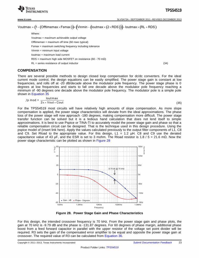
COMPENSATIONThere are several possible methods to design closed loop compensation for dc/dc converters. For the idealcurrent mode control, the design equations can be easily simplified. The power stage gain is constant at lowfrequencies, and rolls off at -20 dB/decade above the modulator pole frequency. The power stage phase is 0degrees at low frequencies and starts to fall one decade above the modulator pole frequency reaching aminimum of -90 degrees one decade above the modulator pole frequency. The modulator pole is a simple poleshown in Equation 35
(35)
For the TPS54519 most circuits will have relatively high amounts of slope compensation. As more slopecompensation is applied, the power stage characteristics will deviate from the ideal approximations. The phaseloss of the power stage will now approach -180 degrees, making compensation more difficult. The power stagetransfer function can be solved but it is a tedious hand calculation that does not lend itself to simpleapproximations. It is best to use Pspice or TINA-TI to accurately model the power stage gain and phase so that areliable compensation circuit can be designed. That is the technique used in this design procedure. Using thepspice model of (insert link here). Apply the values calculated previously to the output filter components of L1, C8and C9. Set Rload to the appropriate value. For this design, L1 = 1.2 µH. C8 and C9 use the deratedcapacitance value of 43 µF, and the ESR is set to 3 mohm. The Rload resistor is 1.8 / 5 = 21.6 mΩ. Now thepower stage characteristic can be plotted as shown in Figure 28
Figure 28. Power Stage Gain and Phase Characteristics
For this design, the intended crossover frequency is 70 kHz. From the power stage gain and phase plots, thegain at 70 kHz is -9.79 dB and the phase is -131.87 degrees. For 60 degrees of phase margin, additional phaseboost from a feed forward capacitor in parallel with the upper resistor of the voltage set point divider will berequired. R3 sets the gain of the compensated error amplifier to be equal and opposite the power stage gain atcrossover. The required value of R3 can be calculated from Equation 36.
Copyright © 2011–2013, Texas Instruments Incorporated Submit Documentation Feedback 23
Product Folder Links: TPS54519

× p × × ×REF
CO
OUT
1C10 =
V2 R6 F
V
× p × × PP
1F =
2 C10 R6 R7
× p × ×Z
1F =
2 C10 R6
× p × × P
1C4 =
2 R3 F
× p × ×CO
1C5 =
F2 R3
10
-
×
PWRSTGG
20out
EA REF
V10R3 =
gm V
TPS54519
SLVSAT3A –SEPTEMBER 2011–REVISED DECEMBER 2013 www.ti.com
(36)
To maximize phase gain, the compensator zero is placed one decade below the crossover frequency of 70 kHz.The required value for C5 is given by Equation 37.
(37)
To maximize phase gain the high frequency pole is not implemented and C4 is not populated. The pole can beuseful to offset the ESR of aluminum electrolytic output capacitors. If desired the value for C4 can be calculatedfrom Equation 38.
(38)
For maximum phase boost, the pole frequency FP will typically be one decade above the intended crossoverfrequency FCO.
The feed forward capacitor C10, is used to increase the phase boost at crossover above what is normallyavailable from Type II compensation. It places an additional zero/pole pair located at Equation 39 andEquation 40.
(39)
(40)
This zero and pole pair is not independent. Once the zero location is chosen, the pole is fixed as well. Foroptimum performance, the zero and pole should be located symmetrically about the intended crossoverfrequency. The required value for C10 can calculated from Equation 41.
(41)
For this design the calculated values for the compensation components are R3 = 23.8 kΩ ,C5 = 959 pF and C10= 197 pF. Using standard values, the compensation components are R3 = 23.7 kΩ ,C5 = 1000 pF and C10 =220 pF.
APPLICATION CURVES
24 Submit Documentation Feedback Copyright © 2011–2013, Texas Instruments Incorporated
Product Folder Links: TPS54519

V = 1 V/divOUT
Time = 2 ms/div
EN = 2 V/div
V = 5 V/divIN
PWRGD = 5 V/div
V = 1 V/divOUT
Time = 2 ms/div
EN = 2 V/div
V = 5 V/divIN
PWRGD = 5 V/div
V = 50 mV/div (ac coupled)OUT
Time = 200 µs/div
I = 2 A/divOUT
Slew rate = 0.5 A/µs
V = 1 V/divOUT
Time = 2 ms/div
EN = 2 V/div
V = 5 V/divIN
PWRGD = 5 V/div
0
10
20
30
40
50
60
70
80
90
100
0 0.5 1 1.5 2 2.5 3 3.5 4 4.5 5Output Current (A)
Effi
cien
cy (
%)
VIN = 3.3 VVIN = 5 V
G001
0
10
20
30
40
50
60
70
80
90
100
0.001 0.01 0.1 1Output Current (A)
Effi
cien
cy (
%)
VIN = 3.3 VVIN = 5 V
G002
TPS54519
www.ti.com SLVSAT3A –SEPTEMBER 2011–REVISED DECEMBER 2013
EFFICIENCY EFFICIENCYvs vs
LOAD CURRENT LOAD CURRENT
Figure 29. Figure 30.
TRANSIENT RESPONSE, 2 A STEP POWER UP VOUT, VIN
Figure 31. Figure 32.
POWER DOWN VOUT, VIN POWER UP VOUT, EN
Figure 33. Figure 34.
Copyright © 2011–2013, Texas Instruments Incorporated Submit Documentation Feedback 25
Product Folder Links: TPS54519

−1
−0.8
−0.6
−0.4
−0.2
0
0.2
0.4
0.6
0.8
1
0 0.5 1 1.5 2 2.5 3 3.5 4 4.5 5Output Current (A)
Out
put V
olta
ge D
evia
tion
(%)
VIN = 3.3 VVIN = 5 V
G003
−0.4
−0.3
−0.2
−0.1
0
0.1
0.2
0.3
0.4
3 3.5 4 4.5 5 5.5 6Input Voltage (V)
Out
put V
olta
ge D
evia
tion
(%)
IOUT = 2.5 A
G004
V = 100 mV/div (ac coupled)IN
Time = 500 ns/div
PH = 2 V/div
100 1000 10000 100000 1000000−60
−50
−40
−30
−20
−10
0
10
20
30
40
50
60
−180
−150
−120
−90
−60
−30
0
30
60
90
120
150
180
Frequency (Hz)
Gai
n (d
B)
Pha
se (
°)
GainPhase
G005
V = 1 V/divOUT
Time = 100 µs/div
EN = 2 V/div
V = 5 V/divIN
PWRGD = 5 V/div
V = 20 mV/div (ac coupled)OUT
Time = 500 ns/div
PH = 2 V/div
TPS54519
SLVSAT3A –SEPTEMBER 2011–REVISED DECEMBER 2013 www.ti.com
POWER DOWN VOUT, EN OUTPUT RIPPLE, 5 A
Figure 35. Figure 36.
INPUT RIPPLE, 5 A CLOSED LOOP RESPONSE, VIN (3.3 V), 4 A
Figure 37. Figure 38.
LOAD REGULATION REGULATIONvs vs
LOAD CURRENT INPUT VOLTAGE
Figure 39. Figure 40.
26 Submit Documentation Feedback Copyright © 2011–2013, Texas Instruments Incorporated
Product Folder Links: TPS54519

I = 5 AOUT
48 °C
23 °C
Maximum Temperature = 58 °C
TPS54519
www.ti.com SLVSAT3A –SEPTEMBER 2011–REVISED DECEMBER 2013
Figure 41. Thermal Image
POWER DISSIPATION ESTIMATEThe following formulas show how to estimate the IC power dissipation under continuous conduction mode (CCM)operation. The power dissipation of the IC (Ptot) includes conduction loss (Pcon), dead time loss (Pd), switchingloss (Psw), gate drive loss (Pgd) and supply current loss (Pq).
Pcon = Io2 × Rdson_temp
Pd = ƒsw × Iout × 0.7 × 40 × 10-9
Psw = 0.5 × Vin × Io × ƒsw × 7 × 10⁻⁹
Pgd = 2 × Vin × 6 × 10⁻⁹ × ƒsw
Pq = 455 × 10-6 × Vin
Where:IOUT is the output current (A).Rdson is the on-resistance of the high-side MOSFET (Ω).VOUT is the output voltage (V).VIN is the input voltage (V).ƒsw is the switching frequency (Hz).
So
Ptot = Pcon + Pd + Psw + Pgd + Pq
For given TA,
TJ = TA + Rth × Ptot
For given TJMAX = 140°C
TAmax = TJ max – Rth × Ptot
Where:Ptot is the total device power dissipation (W).TA is the ambient temperature (°C).TJ is the junction temperature (°C).Rth is the thermal resistance of the package (°C/W).TJMAX is maximum junction temperature (°C).TAMAX is maximum ambient temperature (°C).
There are additional power losses in the regulator circuit due to the inductor AC and DC losses and traceresistance that impact the overall efficiency of the regulator.
Copyright © 2011–2013, Texas Instruments Incorporated Submit Documentation Feedback 27
Product Folder Links: TPS54519

TPS54519
SLVSAT3A –SEPTEMBER 2011–REVISED DECEMBER 2013 www.ti.com
LAYOUTLayout is a critical portion of good power supply design. There are several signal paths that conduct fastchanging currents or voltages that can interact with stray inductance or parasitic capacitance to generate noiseor degrade the power supplies performance. Care should be taken to minimize the loop area formed by thebypass capacitor connections and the VIN pins. See Figure 42 for a PCB layout example. The GND pins andAGND pin should be tied directly to the power pad under the IC. The power pad should be connected to anyinternal PCB ground planes using multiple vias directly under the IC. Additional vias can be used to connect thetop side ground area to the internal planes near the input and output capacitors. For operation at full rated load,the top side ground area along with any additional internal ground planes must provide adequate heat dissipatingarea.
Locate the input bypass capacitor as close to the IC as possible. The PH pin should be routed to the outputinductor. Since the PH connection is the switching node, the output inductor should be located very close to thePH pins, and the area of the PCB conductor minimized to prevent excessive capacitive coupling. The bootcapacitor must also be located close to the device. The sensitive analog ground connections for the feedbackvoltage divider, compensation components, slow start capacitor and frequency set resistor should be connectedto a separate analog ground trace as shown. The RT pin is particularly sensitive to noise so the RT resistorshould be located as close as possible to the IC and routed with minimal lengths of trace. The additional externalcomponents can be placed approximately as shown. It may be possible to obtain acceptable performance withalternate PCB layouts, however this layout has been shown to produce good results and is meant as a guideline.
28 Submit Documentation Feedback Copyright © 2011–2013, Texas Instruments Incorporated
Product Folder Links: TPS54519

VIN
VIN
VIN
GND
EN
GND
VS
EN
SE
SS/TR
PH
PH
PH
PW
RG
D
BO
OT
RT
CO
MP
AG
ND
PH
BOOT
CAPACITOR
VOUTOUTPUT
INDUCTOR
OUTPUT
FILTER
CAPACITOR
SLOW START
CAPACITOR
COMPENSATION
NETWORK
TOPSIDE
GROUND
AREA
VIA to Ground Plane
FREQUENCY
SET
RESISTOR
ANALOG
GROUND
TRACE
VIN
INPUT
BYPASS
CAPACITOR
VIN
UVLO SET
RESISTORS
FEEDBACK
RESISTORS
VIA to
Ground
Plane
EXPOSED
POWERPAD
AREA
TPS54519
www.ti.com SLVSAT3A –SEPTEMBER 2011–REVISED DECEMBER 2013
Figure 42. PCB Layout Example
Copyright © 2011–2013, Texas Instruments Incorporated Submit Documentation Feedback 29
Product Folder Links: TPS54519

TPS54519
SLVSAT3A –SEPTEMBER 2011–REVISED DECEMBER 2013 www.ti.com
REVISION HISTORYNOTE: Page numbers of current revision may differ from previous versions.
Changes from Original (September 2011) to Revision A Page
• Added Voltage Reference spec for Condition "0 A ≤ IOUT ≤ 5 A, 25°C " .............................................................................. 3
30 Submit Documentation Feedback Copyright © 2011–2013, Texas Instruments Incorporated
Product Folder Links: TPS54519

PACKAGE OPTION ADDENDUM
www.ti.com 7-Sep-2016
Addendum-Page 1
PACKAGING INFORMATION
Orderable Device Status(1)
Package Type PackageDrawing
Pins PackageQty
Eco Plan(2)
Lead/Ball Finish(6)
MSL Peak Temp(3)
Op Temp (°C) Device Marking(4/5)
Samples
TPS54519RTER ACTIVE WQFN RTE 16 3000 Green (RoHS& no Sb/Br)
CU NIPDAU Level-2-260C-1 YEAR -40 to 140 54519
TPS54519RTET ACTIVE WQFN RTE 16 250 Green (RoHS& no Sb/Br)
CU NIPDAU Level-2-260C-1 YEAR -40 to 140 54519
(1) The marketing status values are defined as follows:ACTIVE: Product device recommended for new designs.LIFEBUY: TI has announced that the device will be discontinued, and a lifetime-buy period is in effect.NRND: Not recommended for new designs. Device is in production to support existing customers, but TI does not recommend using this part in a new design.PREVIEW: Device has been announced but is not in production. Samples may or may not be available.OBSOLETE: TI has discontinued the production of the device.
(2) Eco Plan - The planned eco-friendly classification: Pb-Free (RoHS), Pb-Free (RoHS Exempt), or Green (RoHS & no Sb/Br) - please check http://www.ti.com/productcontent for the latest availabilityinformation and additional product content details.TBD: The Pb-Free/Green conversion plan has not been defined.Pb-Free (RoHS): TI's terms "Lead-Free" or "Pb-Free" mean semiconductor products that are compatible with the current RoHS requirements for all 6 substances, including the requirement thatlead not exceed 0.1% by weight in homogeneous materials. Where designed to be soldered at high temperatures, TI Pb-Free products are suitable for use in specified lead-free processes.Pb-Free (RoHS Exempt): This component has a RoHS exemption for either 1) lead-based flip-chip solder bumps used between the die and package, or 2) lead-based die adhesive used betweenthe die and leadframe. The component is otherwise considered Pb-Free (RoHS compatible) as defined above.Green (RoHS & no Sb/Br): TI defines "Green" to mean Pb-Free (RoHS compatible), and free of Bromine (Br) and Antimony (Sb) based flame retardants (Br or Sb do not exceed 0.1% by weightin homogeneous material)
(3) MSL, Peak Temp. - The Moisture Sensitivity Level rating according to the JEDEC industry standard classifications, and peak solder temperature.
(4) There may be additional marking, which relates to the logo, the lot trace code information, or the environmental category on the device.
(5) Multiple Device Markings will be inside parentheses. Only one Device Marking contained in parentheses and separated by a "~" will appear on a device. If a line is indented then it is a continuationof the previous line and the two combined represent the entire Device Marking for that device.
(6) Lead/Ball Finish - Orderable Devices may have multiple material finish options. Finish options are separated by a vertical ruled line. Lead/Ball Finish values may wrap to two lines if the finishvalue exceeds the maximum column width.
Important Information and Disclaimer:The information provided on this page represents TI's knowledge and belief as of the date that it is provided. TI bases its knowledge and belief on informationprovided by third parties, and makes no representation or warranty as to the accuracy of such information. Efforts are underway to better integrate information from third parties. TI has taken andcontinues to take reasonable steps to provide representative and accurate information but may not have conducted destructive testing or chemical analysis on incoming materials and chemicals.TI and TI suppliers consider certain information to be proprietary, and thus CAS numbers and other limited information may not be available for release.

PACKAGE OPTION ADDENDUM
www.ti.com 7-Sep-2016
Addendum-Page 2
In no event shall TI's liability arising out of such information exceed the total purchase price of the TI part(s) at issue in this document sold by TI to Customer on an annual basis.

TAPE AND REEL INFORMATION
*All dimensions are nominal
Device PackageType
PackageDrawing
Pins SPQ ReelDiameter
(mm)
ReelWidth
W1 (mm)
A0(mm)
B0(mm)
K0(mm)
P1(mm)
W(mm)
Pin1Quadrant
TPS54519RTER WQFN RTE 16 3000 330.0 12.4 3.3 3.3 1.1 8.0 12.0 Q2
TPS54519RTET WQFN RTE 16 250 180.0 12.4 3.3 3.3 1.1 8.0 12.0 Q2
PACKAGE MATERIALS INFORMATION
www.ti.com 13-Dec-2013
Pack Materials-Page 1

*All dimensions are nominal
Device Package Type Package Drawing Pins SPQ Length (mm) Width (mm) Height (mm)
TPS54519RTER WQFN RTE 16 3000 367.0 367.0 35.0
TPS54519RTET WQFN RTE 16 250 210.0 185.0 35.0
PACKAGE MATERIALS INFORMATION
www.ti.com 13-Dec-2013
Pack Materials-Page 2


IMPORTANT NOTICE
Texas Instruments Incorporated and its subsidiaries (TI) reserve the right to make corrections, enhancements, improvements and otherchanges to its semiconductor products and services per JESD46, latest issue, and to discontinue any product or service per JESD48, latestissue. Buyers should obtain the latest relevant information before placing orders and should verify that such information is current andcomplete. All semiconductor products (also referred to herein as “components”) are sold subject to TI’s terms and conditions of salesupplied at the time of order acknowledgment.TI warrants performance of its components to the specifications applicable at the time of sale, in accordance with the warranty in TI’s termsand conditions of sale of semiconductor products. Testing and other quality control techniques are used to the extent TI deems necessaryto support this warranty. Except where mandated by applicable law, testing of all parameters of each component is not necessarilyperformed.TI assumes no liability for applications assistance or the design of Buyers’ products. Buyers are responsible for their products andapplications using TI components. To minimize the risks associated with Buyers’ products and applications, Buyers should provideadequate design and operating safeguards.TI does not warrant or represent that any license, either express or implied, is granted under any patent right, copyright, mask work right, orother intellectual property right relating to any combination, machine, or process in which TI components or services are used. Informationpublished by TI regarding third-party products or services does not constitute a license to use such products or services or a warranty orendorsement thereof. Use of such information may require a license from a third party under the patents or other intellectual property of thethird party, or a license from TI under the patents or other intellectual property of TI.Reproduction of significant portions of TI information in TI data books or data sheets is permissible only if reproduction is without alterationand is accompanied by all associated warranties, conditions, limitations, and notices. TI is not responsible or liable for such altereddocumentation. Information of third parties may be subject to additional restrictions.Resale of TI components or services with statements different from or beyond the parameters stated by TI for that component or servicevoids all express and any implied warranties for the associated TI component or service and is an unfair and deceptive business practice.TI is not responsible or liable for any such statements.Buyer acknowledges and agrees that it is solely responsible for compliance with all legal, regulatory and safety-related requirementsconcerning its products, and any use of TI components in its applications, notwithstanding any applications-related information or supportthat may be provided by TI. Buyer represents and agrees that it has all the necessary expertise to create and implement safeguards whichanticipate dangerous consequences of failures, monitor failures and their consequences, lessen the likelihood of failures that might causeharm and take appropriate remedial actions. Buyer will fully indemnify TI and its representatives against any damages arising out of the useof any TI components in safety-critical applications.In some cases, TI components may be promoted specifically to facilitate safety-related applications. With such components, TI’s goal is tohelp enable customers to design and create their own end-product solutions that meet applicable functional safety standards andrequirements. Nonetheless, such components are subject to these terms.No TI components are authorized for use in FDA Class III (or similar life-critical medical equipment) unless authorized officers of the partieshave executed a special agreement specifically governing such use.Only those TI components which TI has specifically designated as military grade or “enhanced plastic” are designed and intended for use inmilitary/aerospace applications or environments. Buyer acknowledges and agrees that any military or aerospace use of TI componentswhich have not been so designated is solely at the Buyer's risk, and that Buyer is solely responsible for compliance with all legal andregulatory requirements in connection with such use.TI has specifically designated certain components as meeting ISO/TS16949 requirements, mainly for automotive use. In any case of use ofnon-designated products, TI will not be responsible for any failure to meet ISO/TS16949.
Products ApplicationsAudio www.ti.com/audio Automotive and Transportation www.ti.com/automotiveAmplifiers amplifier.ti.com Communications and Telecom www.ti.com/communicationsData Converters dataconverter.ti.com Computers and Peripherals www.ti.com/computersDLP® Products www.dlp.com Consumer Electronics www.ti.com/consumer-appsDSP dsp.ti.com Energy and Lighting www.ti.com/energyClocks and Timers www.ti.com/clocks Industrial www.ti.com/industrialInterface interface.ti.com Medical www.ti.com/medicalLogic logic.ti.com Security www.ti.com/securityPower Mgmt power.ti.com Space, Avionics and Defense www.ti.com/space-avionics-defenseMicrocontrollers microcontroller.ti.com Video and Imaging www.ti.com/videoRFID www.ti-rfid.comOMAP Applications Processors www.ti.com/omap TI E2E Community e2e.ti.comWireless Connectivity www.ti.com/wirelessconnectivity
Mailing Address: Texas Instruments, Post Office Box 655303, Dallas, Texas 75265Copyright © 2016, Texas Instruments Incorporated