Embed Size (px)
Citation preview

IOUT (A)
Effi
cien
cy (
%)
1E-5 0.0001 0.001 0.01 0.1 1 1040
50
60
70
80
90
100
LMR2
VOUT = 5 VVOUT = 3.3 V
BOOT
SW
LCBOOT
FB
VIN
VIN up to 36 V
PGND
COUT
EN/SYNC
CIN
VCC
AGNDVOUT
CVCC
RFBT
RFBB
Copyright © 2017, Texas Instruments Incorporated
Product
Folder
Order
Now
Technical
Documents
Tools &
Software
Support &Community
An IMPORTANT NOTICE at the end of this data sheet addresses availability, warranty, changes, use in safety-critical applications,intellectual property matters and other important disclaimers. PRODUCTION DATA.
LMR23615SNVSAV8A –JUNE 2017–REVISED FEBRUARY 2018
LMR23615 SIMPLE SWITCHER® 36-V, 1.5-A Synchronous Step-Down Converter
1
1 Features1• 4-V to 36-V Input Range• 1.5-A Continuous Output Current• Integrated Synchronous Rectification• Current-Mode Control with internal compensation• Minimum Switch ON-Time: 60 ns• Adjustable Switching Frequency• PFM Mode at Light Load• Frequency Synchronization to External Clock• 75-µA Quiescent Current• Soft Start into a Prebiased Load• High-Duty-Cycle Operation Supported• Output Short-Circuit Protection With Hiccup Mode• Thermal Protection• 12-Pin WSON Wettable Flanks Package With
PowerPAD™• Create a Custom Design Using the LMR23615
With the WEBENCH® Power Designer
2 Applications• Factory and Building Automation Systems: PLC
CPU, HVAC Control, Elevator Control• GSM, GPRS Modules for Fleet Management,
Smart Grids, and Security• General Purpose Wide VIN Regulation
space
3 DescriptionThe LMR23615 SIMPLE SWITCHER® is an easy-to-use 36-V, 1.5-A synchronous step-down regulator.With a wide input range from 4 V to 36 V, the deviceis suitable for various industrial applications for powerconditioning from unregulated sources. Peak currentmode control is employed to achieve simple control-loop compensation and cycle-by-cycle currentlimiting. A quiescent current of 75 µA makes thedevice suitable for battery-powered systems. An ultra-low 2-µA shutdown current can further prolongbattery life. Internal loop compensation means thatthe user is free from the tedious task of loop-compensation design and also minimizes the externalcomponents needed. An extended family is availablein 2.5-A (LMR23625) and 3-A (LMR23630) load-current options in pin-to-pin compatible packages,allowing simple, optimum PCB layout. A precisionenable input allows simplification of regulator controland system power sequencing. Protection featuresinclude cycle-by-cycle current limit, hiccup-modeshort-circuit protection, and thermal shutdown due toexcessive power dissipation.
Device Information(1)
PART NUMBER PACKAGE BODY SIZE (NOM)LMR23615 WSON (12) 3.00 mm × 3.00 mm
(1) For all available packages, see the orderable addendum atthe end of the data sheet.
space
space
spaceSimplified Schematic
Efficiency vs Load, VIN = 12 V

2
LMR23615SNVSAV8A –JUNE 2017–REVISED FEBRUARY 2018 www.ti.com
Product Folder Links: LMR23615
Submit Documentation Feedback Copyright © 2017–2018, Texas Instruments Incorporated
Table of Contents1 Features .................................................................. 12 Applications ........................................................... 13 Description ............................................................. 14 Revision History..................................................... 25 Pin Configuration and Functions ......................... 36 Specifications......................................................... 4
6.1 Absolute Maximum Ratings ...................................... 46.2 ESD Ratings.............................................................. 46.3 Recommended Operating Conditions ...................... 46.4 Thermal Information .................................................. 56.5 Electrical Characteristics........................................... 56.6 Timing Characteristics............................................... 66.7 Switching Characteristics .......................................... 66.8 Typical Characteristics .............................................. 7
7 Detailed Description .............................................. 97.1 Overview ................................................................... 97.2 Functional Block Diagram ......................................... 9
7.3 Feature Description................................................. 107.4 Device Functional Modes........................................ 16
8 Application and Implementation ........................ 178.1 Application Information............................................ 178.2 Typical Applications ................................................ 17
9 Power Supply Recommendations ...................... 2310 Layout................................................................... 24
10.1 Layout Guidelines ................................................. 2410.2 Layout Example .................................................... 26
11 Device and Documentation Support ................. 2711.1 Device Support...................................................... 2711.2 Receiving Notification of Documentation Updates 2711.3 Community Resources.......................................... 2711.4 Trademarks ........................................................... 2711.5 Electrostatic Discharge Caution............................ 2711.6 Glossary ................................................................ 27
12 Mechanical, Packaging, and OrderableInformation ........................................................... 28
4 Revision HistoryNOTE: Page numbers for previous revisions may differ from page numbers in the current version.
Changes from Original (June 2017) to Revision A Page
• First release of production-data data sheet; added WEBENCH content .............................................................................. 1• Changed Programmable Logic Controller Power Supply to Factory and Building Automation System... in
Applications ........................................................................................................................................................................... 1• Deleted Multi-Function Printers and Industrial Power Supplies and reworded Applications.................................................. 1• Changed HVAC Systems from Applications to General Purpose Wide VIN Regulation ...................................................... 1• Changed the BOOT Capacitor value on Pin Functions to indicate value from 470nF to 100nF or higher ............................ 3• Change the Abs Max Rating for EN/SYNC to AGND to VIN + 0.3 from 42V.......................................................................... 4• Changed Typical Value for VIN_UVLO Rising threshold typical from 3.6-V to 3.7-V and minimum Falling threshold
from 3-V to 2.9-V ................................................................................................................................................................... 5• Change Figure 20 from VOUT = 5 V, fSW = 1600 kHz to VOUT = 5 V, fSW = 2100 kHz ........................................................... 14• Changed from VOUT = 7 V to 36 V to VIN = 7 V to 36 V on Figure 28................................................................................... 22

SW
SW
BOOT
VCC
FB
RT
PGND
NC
VIN
VIN
EN/SYNC
AGND
1
2
3
4
5
6
12
11
10
9
8
7
PAD13
3
LMR23615www.ti.com SNVSAV8A –JUNE 2017–REVISED FEBRUARY 2018
Product Folder Links: LMR23615
Submit Documentation FeedbackCopyright © 2017–2018, Texas Instruments Incorporated
5 Pin Configuration and Functions
DRR Package12-Pin WSON With Thermal Pad
Top View
Pin FunctionsPIN
I/O DESCRIPTIONNUMBER NAME
1, 2 SW P Switching output of the regulator. Internally connected to both power MOSFETs. Connect topower inductor.
3 BOOT P Boot-strap capacitor connection for high-side driver. Connect a high-quality 100nF to 470nFcapacitor from BOOT to SW.
4 VCC P Internal bias supply output for bypassing. Connect bypass capacitor from this pin to AGND. Donot connect external loading to this pin. Never short this pin to ground during operation.
5 FB A Feedback input to regulator, connect the feedback resistor divider tap to this pin.
6 RT A Connect a resistor RT from this pin to AGND to program switching frequency. Leave floatingfor 400-kHz default switching frequency.
7 AGND G Analog ground pin. Ground reference for internal references and logic. Connect to systemground.
8 EN/SYNC A
Enable input to regulator. High=On, Low=Off. Can be connected to VIN. Do not float. Adjustthe input under voltage lockout with two resistors. The internal oscillator can be synchronizedto an external clock by coupling a positive pulse into this pin through a small couplingcapacitor. See Enable/Sync for detail.
9, 10 VIN P Input supply voltage.11 NC N/A Not for use. Leave this pin floating.
12 PGND G Power ground pin, connected internally to the low side power FET. Connect to system ground,PAD, AGND, ground pins of CIN and COUT. Path to CIN must be as short as possible.
13 PAD G Low impedance connection to AGND. Connect to PGND on PCB. Major heat dissipation pathof the die. Must be used for heat sinking to ground plane on PCB.
4
LMR23615SNVSAV8A –JUNE 2017–REVISED FEBRUARY 2018 www.ti.com
Product Folder Links: LMR23615
Submit Documentation Feedback Copyright © 2017–2018, Texas Instruments Incorporated
(1) Stresses beyond those listed under Absolute Maximum Ratings may cause permanent damage to the device. These are stress ratingsonly, which do not imply functional operation of the device at these or any other conditions beyond those indicated under RecommendedOperating Conditions. Exposure to absolute-maximum-rated conditions for extended periods may affect device reliability.
(2) In shutdown mode, the VCC to AGND maximum value is 5.25 V.
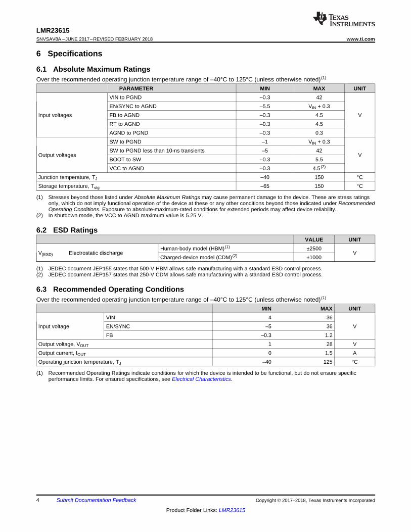
6 Specifications
6.1 Absolute Maximum RatingsOver the recommended operating junction temperature range of –40°C to 125°C (unless otherwise noted) (1)
PARAMETER MIN MAX UNIT
Input voltages
VIN to PGND –0.3 42
VEN/SYNC to AGND –5.5 VIN + 0.3FB to AGND –0.3 4.5RT to AGND –0.3 4.5AGND to PGND –0.3 0.3
Output voltages
SW to PGND –1 VIN + 0.3
VSW to PGND less than 10-ns transients –5 42BOOT to SW –0.3 5.5VCC to AGND –0.3 4.5 (2)
Junction temperature, TJ –40 150 °CStorage temperature, Tstg –65 150 °C
(1) JEDEC document JEP155 states that 500-V HBM allows safe manufacturing with a standard ESD control process.(2) JEDEC document JEP157 states that 250-V CDM allows safe manufacturing with a standard ESD control process.
6.2 ESD RatingsVALUE UNIT
V(ESD) Electrostatic dischargeHuman-body model (HBM) (1) ±2500
VCharged-device model (CDM) (2) ±1000
(1) Recommended Operating Ratings indicate conditions for which the device is intended to be functional, but do not ensure specificperformance limits. For ensured specifications, see Electrical Characteristics.
6.3 Recommended Operating ConditionsOver the recommended operating junction temperature range of –40°C to 125°C (unless otherwise noted) (1)
MIN MAX UNIT
Input voltageVIN 4 36
VEN/SYNC –5 36FB –0.3 1.2
Output voltage, VOUT 1 28 VOutput current, IOUT 0 1.5 AOperating junction temperature, TJ –40 125 °C
5
LMR23615www.ti.com SNVSAV8A –JUNE 2017–REVISED FEBRUARY 2018
Product Folder Links: LMR23615
Submit Documentation FeedbackCopyright © 2017–2018, Texas Instruments Incorporated
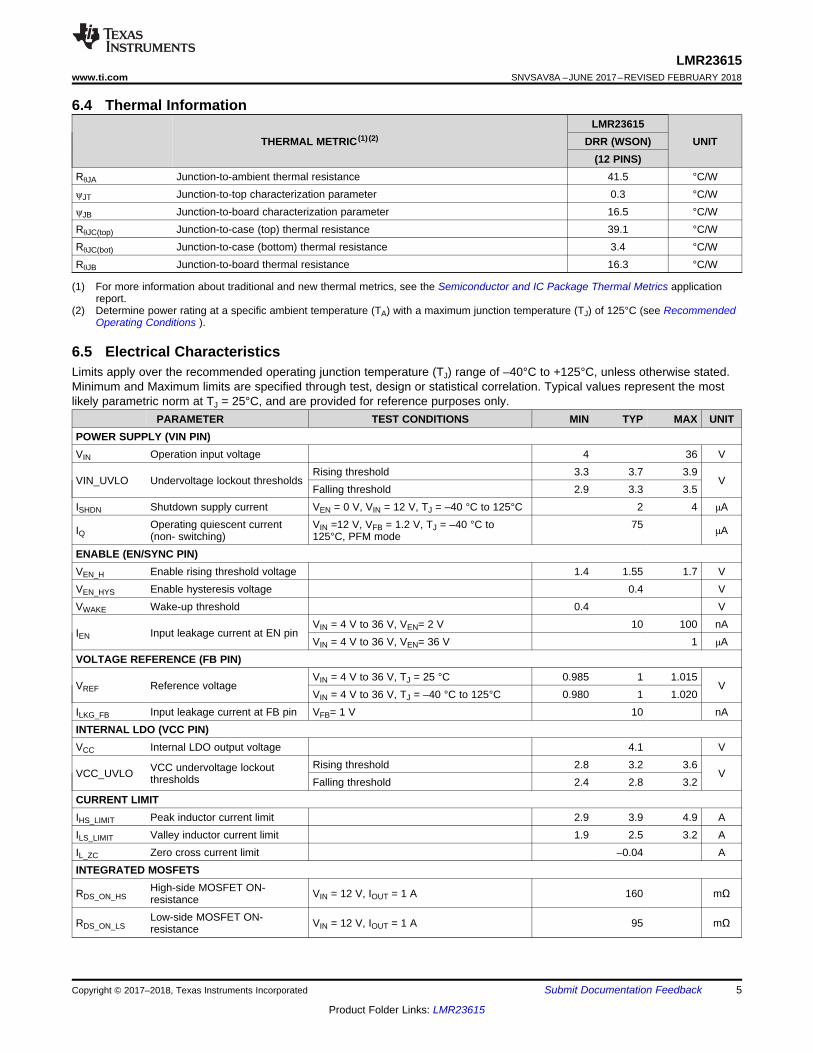
(1) For more information about traditional and new thermal metrics, see the Semiconductor and IC Package Thermal Metrics applicationreport.
(2) Determine power rating at a specific ambient temperature (TA) with a maximum junction temperature (TJ) of 125°C (see RecommendedOperating Conditions ).
6.4 Thermal Information
THERMAL METRIC (1) (2)LMR23615
UNITDRR (WSON)(12 PINS)
RθJA Junction-to-ambient thermal resistance 41.5 °C/WψJT Junction-to-top characterization parameter 0.3 °C/WψJB Junction-to-board characterization parameter 16.5 °C/WRθJC(top) Junction-to-case (top) thermal resistance 39.1 °C/WRθJC(bot) Junction-to-case (bottom) thermal resistance 3.4 °C/WRθJB Junction-to-board thermal resistance 16.3 °C/W
6.5 Electrical CharacteristicsLimits apply over the recommended operating junction temperature (TJ) range of –40°C to +125°C, unless otherwise stated.Minimum and Maximum limits are specified through test, design or statistical correlation. Typical values represent the mostlikely parametric norm at TJ = 25°C, and are provided for reference purposes only.
PARAMETER TEST CONDITIONS MIN TYP MAX UNITPOWER SUPPLY (VIN PIN)VIN Operation input voltage 4 36 V
VIN_UVLO Undervoltage lockout thresholdsRising threshold 3.3 3.7 3.9
VFalling threshold 2.9 3.3 3.5
ISHDN Shutdown supply current VEN = 0 V, VIN = 12 V, TJ = –40 °C to 125°C 2 4 μA
IQOperating quiescent current(non- switching)
VIN =12 V, VFB = 1.2 V, TJ = –40 °C to125°C, PFM mode
75 μA
ENABLE (EN/SYNC PIN)VEN_H Enable rising threshold voltage 1.4 1.55 1.7 VVEN_HYS Enable hysteresis voltage 0.4 VVWAKE Wake-up threshold 0.4 V
IEN Input leakage current at EN pinVIN = 4 V to 36 V, VEN= 2 V 10 100 nAVIN = 4 V to 36 V, VEN= 36 V 1 μA
VOLTAGE REFERENCE (FB PIN)
VREF Reference voltageVIN = 4 V to 36 V, TJ = 25 °C 0.985 1 1.015
VVIN = 4 V to 36 V, TJ = –40 °C to 125°C 0.980 1 1.020
ILKG_FB Input leakage current at FB pin VFB= 1 V 10 nAINTERNAL LDO (VCC PIN)VCC Internal LDO output voltage 4.1 V
VCC_UVLO VCC undervoltage lockoutthresholds
Rising threshold 2.8 3.2 3.6V
Falling threshold 2.4 2.8 3.2CURRENT LIMITIHS_LIMIT Peak inductor current limit 2.9 3.9 4.9 AILS_LIMIT Valley inductor current limit 1.9 2.5 3.2 AIL_ZC Zero cross current limit –0.04 AINTEGRATED MOSFETS
RDS_ON_HSHigh-side MOSFET ON-resistance VIN = 12 V, IOUT = 1 A 160 mΩ
RDS_ON_LSLow-side MOSFET ON-resistance VIN = 12 V, IOUT = 1 A 95 mΩ
6
LMR23615SNVSAV8A –JUNE 2017–REVISED FEBRUARY 2018 www.ti.com
Product Folder Links: LMR23615
Submit Documentation Feedback Copyright © 2017–2018, Texas Instruments Incorporated
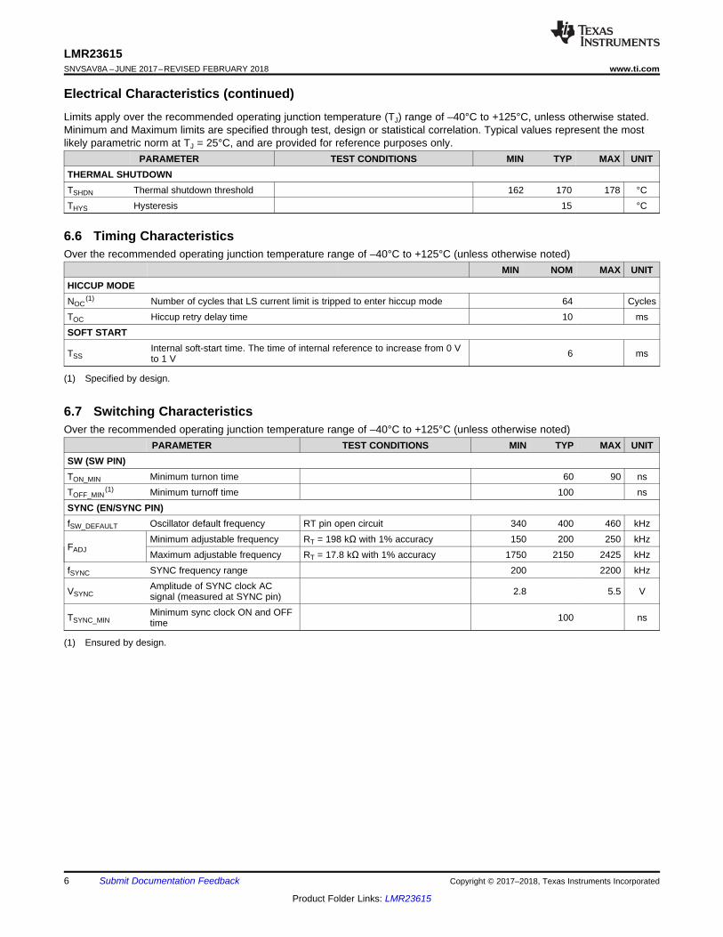
Electrical Characteristics (continued)Limits apply over the recommended operating junction temperature (TJ) range of –40°C to +125°C, unless otherwise stated.Minimum and Maximum limits are specified through test, design or statistical correlation. Typical values represent the mostlikely parametric norm at TJ = 25°C, and are provided for reference purposes only.
PARAMETER TEST CONDITIONS MIN TYP MAX UNITTHERMAL SHUTDOWNTSHDN Thermal shutdown threshold 162 170 178 °CTHYS Hysteresis 15 °C
(1) Specified by design.
6.6 Timing CharacteristicsOver the recommended operating junction temperature range of –40°C to +125°C (unless otherwise noted)
MIN NOM MAX UNITHICCUP MODENOC
(1) Number of cycles that LS current limit is tripped to enter hiccup mode 64 CyclesTOC Hiccup retry delay time 10 msSOFT START
TSSInternal soft-start time. The time of internal reference to increase from 0 Vto 1 V 6 ms
(1) Ensured by design.
6.7 Switching CharacteristicsOver the recommended operating junction temperature range of –40°C to +125°C (unless otherwise noted)
PARAMETER TEST CONDITIONS MIN TYP MAX UNITSW (SW PIN)TON_MIN Minimum turnon time 60 90 nsTOFF_MIN
(1) Minimum turnoff time 100 nsSYNC (EN/SYNC PIN)fSW_DEFAULT Oscillator default frequency RT pin open circuit 340 400 460 kHz
FADJMinimum adjustable frequency RT = 198 kΩ with 1% accuracy 150 200 250 kHzMaximum adjustable frequency RT = 17.8 kΩ with 1% accuracy 1750 2150 2425 kHz
fSYNC SYNC frequency range 200 2200 kHz
VSYNCAmplitude of SYNC clock ACsignal (measured at SYNC pin) 2.8 5.5 V
TSYNC_MINMinimum sync clock ON and OFFtime 100 ns

IOUT (A)
VO
UT (
V)
0 0.2 0.4 0.6 0.8 1 1.2 1.4 1.65.01
5.02
5.03
5.04
5.05
5.06
5.07
5.08
5.09
5.1
5.11
5.12
LMR2
VIN = 12 VVIN = 24 VVIN = 36 V
VIN (V)
VO
UT (
V)
5 10 15 20 25 30 35 405.01
5.02
5.03
5.04
5.05
5.06
5.07
5.08
5.09
5.1
LMR2
IOUT = 1.5 AIOUT = 0.2 AIOUT = 0 A
IOUT (A)
Effi
cien
cy (
%)
1E-5 0.0001 0.001 0.01 0.1 1 100
10
20
30
40
50
60
70
80
90
100
LMR2
VIN = 8 VVIN = 12 VVIN = 24 V
IOUT (A)
Effi
cien
cy (
%)
1E-5 0.0001 0.001 0.01 0.1 1 100
10
20
30
40
50
60
70
80
90
100
LMR2
VIN = 8 VVIN = 12 VVIN = 20 V
IOUT (A)
Effi
cien
cy (
%)
1E-5 0.0001 0.001 0.01 0.1 1 100
10
20
30
40
50
60
70
80
90
100
LMR2
VIN = 12 VVIN = 24 VVIN = 36 V
IOUT (A)
Effi
cien
cy (
%)
1E-5 0.0001 0.001 0.01 0.1 1 100
10
20
30
40
50
60
70
80
90
100
LMR2
VIN = 8 VVIN = 12 VVIN = 24 V
7
LMR23615www.ti.com SNVSAV8A –JUNE 2017–REVISED FEBRUARY 2018
Product Folder Links: LMR23615
Submit Documentation FeedbackCopyright © 2017–2018, Texas Instruments Incorporated
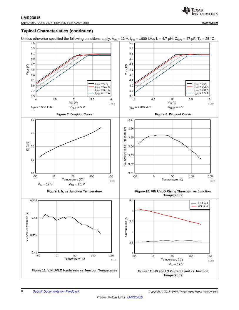
6.8 Typical CharacteristicsUnless otherwise specified the following conditions apply: VIN = 12 V, fSW = 1600 kHz, L = 4.7 µH, COUT = 47 µF, TA = 25 °C.
fSW = 1000 kHz VOUT = 5 V
Figure 1. Efficiency vs Load Current
fSW = 1000 kHz VOUT = 3.3 V
Figure 2. Efficiency vs Load Current
fSW = 2200 kHz VOUT = 5 V
Figure 3. Efficiency vs Load Current
fSW = 2200 kHz(Sync)
VOUT = 3.3 V
Figure 4. Efficiency vs Load Current
fSW = 1000 kHz VOUT = 5 V
Figure 5. Load Regulation
fSW = 1000 kHz VOUT = 5 V
Figure 6. Line Regulation
Temperature (qC)
Cur
rent
Lim
it (A
)
-50 0 50 100 1502
2.5
3
3.5
4
4.5
LMR2
LS LimitHS Limit
Temperature (°C)
VIN
UV
LO H
yste
resi
s (V
)
-50 0 50 100 1500.41
0.415
0.42
0.425
D010
Temperature (°C)
IQ (
µA
)
-50 0 50 100 15060
65
70
75
80
D008Temperature (°C)
VIN
UV
LO R
isin
g T
hres
hold
(V
)
-50 0 50 100 1503.61
3.62
3.63
3.64
3.65
3.66
3.67
D009
VIN (V)
VO
UT (
V)
4 4.5 5 5.5 63.5
3.7
3.9
4.1
4.3
4.5
4.7
4.9
5.1
5.3
5.5
LMR2
IOUT = 0 AIOUT = 0.2 AIOUT = 0.8 AIOUT = 1.5 A
VIN (V)
VO
UT (
V)
4 4.5 5 5.5 63.5
3.7
3.9
4.1
4.3
4.5
4.7
4.9
5.1
5.3
5.5
LMR2
IOUT = 0 AIOUT = 0.2 AIOUT = 0.8 AIOUT = 1.5 A
8
LMR23615SNVSAV8A –JUNE 2017–REVISED FEBRUARY 2018 www.ti.com
Product Folder Links: LMR23615
Submit Documentation Feedback Copyright © 2017–2018, Texas Instruments Incorporated
Typical Characteristics (continued)Unless otherwise specified the following conditions apply: VIN = 12 V, fSW = 1600 kHz, L = 4.7 µH, COUT = 47 µF, TA = 25 °C.
fSW = 1000 kHz VOUT = 5 V
Figure 7. Dropout Curve
fSW = 2200 kHz VOUT = 5 V
Figure 8. Dropout Curve
VIN = 12 V VFB = 1.1 V
Figure 9. IQ vs Junction Temperature Figure 10. VIN UVLO Rising Threshold vs JunctionTemperature
Figure 11. VIN UVLO Hysteresis vs Junction Temperature
VIN = 12 V
Figure 12. HS and LS Current Limit vs JunctionTemperature
EA
REF
EN/SYNC
SW
CBOOT
VCC
InternalSS
OV/UVDetector
Oscillator
PrecisionEnable
LDO
PFMDetector
SlopeComp
PWM CONTROL LOGIC
UVLOTSD
FreqFoldback
ZeroCross
HICCUPDetector
VIN
Rc
Cc
PGND
FB
LS I Sense
HS I Sense
FB
VCCEnable
SYNCDetector
SYNC Signal
SYNC Signal
AGND
RT
Copyright © 2017, Texas Instruments Incorporated
9
LMR23615www.ti.com SNVSAV8A –JUNE 2017–REVISED FEBRUARY 2018
Product Folder Links: LMR23615
Submit Documentation FeedbackCopyright © 2017–2018, Texas Instruments Incorporated
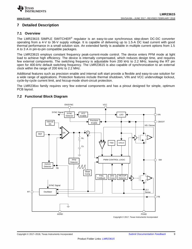
7 Detailed Description
7.1 OverviewThe LMR23615 SIMPLE SWITCHER® regulator is an easy-to-use synchronous step-down DC-DC converteroperating from a 4-V to 36-V supply voltage. It is capable of delivering up to 1.5-A DC load current with goodthermal performance in a small solution size. An extended family is available in multiple current options from 1.5A to 3 A in pin-to-pin compatible packages.
The LMR23615 employs constant frequency peak-current-mode control. The device enters PFM mode at lightload to achieve high efficiency. The device is internally compensated, which reduces design time, and requiresfew external components. The switching frequency is adjustable from 200 kHz to 2.2 MHz, leaving the RT pinopen for 400-kHz default switching frequency. The LMR23615 is also capable of synchronization to an externalclock within the range of 200 kHz to 2.2 MHz.
Additional features such as precision enable and internal soft start provide a flexible and easy-to-use solution fora wide range of applications. Protection features include thermal shutdown, VIN and VCC undervoltage lockout,cycle-by-cycle current limit, and hiccup-mode short-circuit protection.
The LMR236xx family requires very few external components and has a pinout designed for simple, optimumPCB layout.
7.2 Functional Block Diagram

VSW
VIN
D = tON/ TSW
tON tOFF
TSW
t
-VD
0
SW
Vol
tage
iL
IOUT
t0
Indu
ctor
Cur
rent ILPK
'iL
10
LMR23615SNVSAV8A –JUNE 2017–REVISED FEBRUARY 2018 www.ti.com
Product Folder Links: LMR23615
Submit Documentation Feedback Copyright © 2017–2018, Texas Instruments Incorporated
7.3 Feature Description
7.3.1 Fixed-Frequency, Peak-Current-Mode ControlThe following operating description of the LMR23615 refers to the Functional Block Diagram and to thewaveforms in Figure 13. The LMR23615 device is a step-down, synchronous buck regulator with integrated high-side (HS) and low-side (LS) switches (synchronous rectifier). The LMR23615 supplies a regulated output voltageby turning on the HS and LS NMOS switches with controlled duty cycle. During high-side switch ON-time, theSW pin voltage swings up to approximately VIN, and the inductor current IL increase with linear slope (VIN – VOUT)/ L. When the HS switch is turned off by the control logic, the LS switch is turned on after an anti-shoot-throughdead time. Inductor current discharges through the LS switch with a slope of –VOUT / L. The control parameter ofa buck converter is defined as duty cycle D = tON / TSW, where tON is the high-side switch ON time and TSW is theswitching period. The regulator control loop maintains a constant output voltage by adjusting the duty cycle D. Inan ideal buck converter, where losses are ignored, D is proportional to the output voltage and inverselyproportional to the input voltage: D = VOUT / VIN.
Figure 13. SW Node and Inductor Current Waveforms inContinuous Conduction Mode (CCM)
The LMR23615 employs fixed-frequency peak-current-mode control. A voltage-feedback loop is used to getaccurate DC voltage regulation by adjusting the peak current command based on voltage offset. The peakinductor current is sensed from the high-side switch and compared to the peak current threshold to control theon-time of the high-side switch. The voltage feedback loop is internally compensated, which allows for fewerexternal components, makes it easy to design, and provides stable operation with almost any combination ofoutput capacitors. The regulator operates with fixed switching frequency at normal load condition. At light loadcondition, the LMR23615 operates in PFM mode to maintain high efficiency.
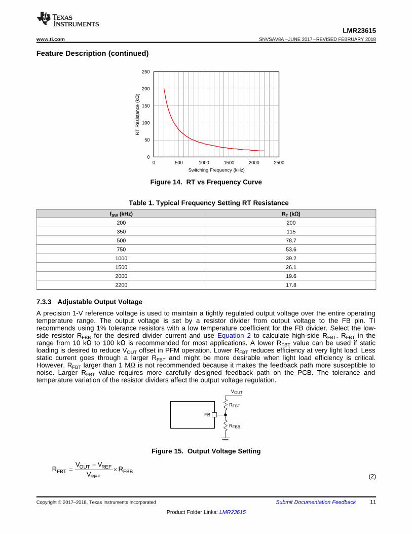
7.3.2 Adjustable FrequencyThe switching frequency can be programmed by the resistor from the RT pin to ground. The frequency isinversely proportional to the RT resistance. The RT pin can be left floating, and the LMR23615 operates at 400-kHz default switching frequency. The RT pin is not designed to be shorted to ground. For a desired frequency,typical RT resistance can be found by Equation 1. Table 1 gives typical RT values for a given switching frequency(fSW ).
RT(kΩ) = 40200 / fSW(kHz) – 0.6 (1)
OUT REFFBT FBB
REF
V VR R
V
u
VOUT
FB
RFBT
RFBB
0
50
100
150
200
250
0 500 1000 1500 2000 2500
RT
Res
ista
nce
(k
)
Switching Frequency (kHz) C008
11
LMR23615www.ti.com SNVSAV8A –JUNE 2017–REVISED FEBRUARY 2018
Product Folder Links: LMR23615
Submit Documentation FeedbackCopyright © 2017–2018, Texas Instruments Incorporated
Feature Description (continued)
Figure 14. RT vs Frequency Curve
Table 1. Typical Frequency Setting RT ResistancefSW (kHz) RT (kΩ)
200 200350 115500 78.7750 53.61000 39.21500 26.12000 19.62200 17.8
7.3.3 Adjustable Output VoltageA precision 1-V reference voltage is used to maintain a tightly regulated output voltage over the entire operatingtemperature range. The output voltage is set by a resistor divider from output voltage to the FB pin. TIrecommends using 1% tolerance resistors with a low temperature coefficient for the FB divider. Select the low-side resistor RFBB for the desired divider current and use Equation 2 to calculate high-side RFBT. RFBT in therange from 10 kΩ to 100 kΩ is recommended for most applications. A lower RFBT value can be used if staticloading is desired to reduce VOUT offset in PFM operation. Lower RFBT reduces efficiency at very light load. Lessstatic current goes through a larger RFBT and might be more desirable when light load efficiency is critical.However, RFBT larger than 1 MΩ is not recommended because it makes the feedback path more susceptible tonoise. Larger RFBT value requires more carefully designed feedback path on the PCB. The tolerance andtemperature variation of the resistor dividers affect the output voltage regulation.
Figure 15. Output Voltage Setting
(2)

RENT
ClockSource
EN/SYNC
CSYNC
VIN
RENB
RENT
EN/SYNC
VIN
RENB
12
LMR23615SNVSAV8A –JUNE 2017–REVISED FEBRUARY 2018 www.ti.com
Product Folder Links: LMR23615
Submit Documentation Feedback Copyright © 2017–2018, Texas Instruments Incorporated
7.3.4 Enable/SyncThe voltage on the EN pin controls the ON or OFF operation of LMR23615 device. A voltage less than 1 V(typical) shuts down the device while a voltage higher than 1.6 V (typical) is required to start the regulator. TheEN pin is an input and cannot be left open or floating. The simplest way to enable the operation of theLMR23615 is to connect the EN to VIN. This allows self-start-up of the LMR23615 when VIN is within theoperation range.
Many applications benefit from the employment of an enable divider RENT and RENB (Figure 16) to establish aprecision system UVLO level for the converter. System UVLO can be used for supplies operating from utilitypower as well as battery power. It can be used for sequencing, ensuring reliable operation, or supply protection,such as a battery discharge level. An external logic signal can also be used to drive EN input for systemsequencing and protection.
Figure 16. System UVLO by Enable Divider
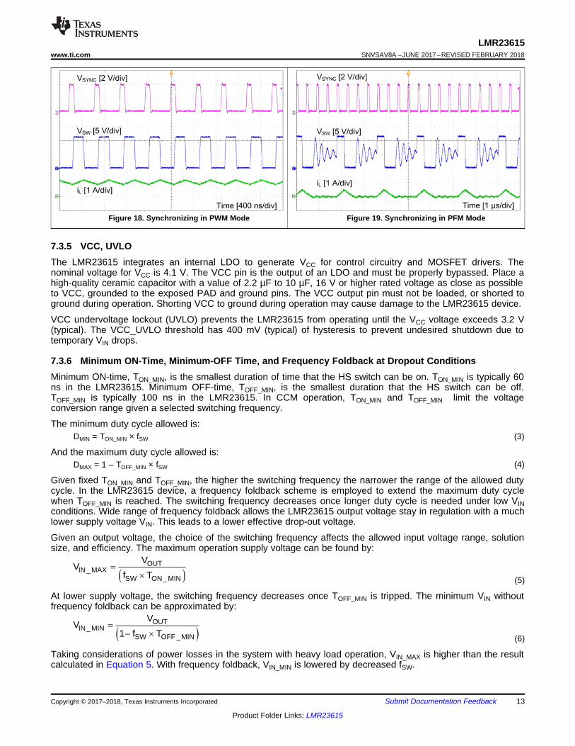
The EN pin also can be used to synchronize the internal oscillator to an external clock. The internal oscillator canbe synchronized by AC coupling a positive edge into the EN pin. The AC coupled peak-to-peak voltage at the ENpin must exceed the SYNC amplitude threshold of 2.8 V (typical) to trip the internal synchronization pulsedetector, and the minimum SYNC clock ON and OFF time must be longer than 100 ns (typical). A 3.3-V or ahigher amplitude pulse signal coupled through a 1-nF capacitor CSYNC is a good starting point. Keeping RENT //RENB (RENT parallel with RENB) in the 100-kΩ range is a good choice. RENT is required for this synchronizationcircuit, but RENB can be left unmounted if system UVLO is not needed. Switching action of the LMR23615 devicecan be synchronized to an external clock from 200 kHz to 2.2 MHz. Figure 18 and Figure 19 show the devicesynchronized to an external system clock.
Figure 17. Synchronizing to External Clock
OUT
IN_MINSW OFF _MIN
VV
1 f T
u
OUT
IN_MAXSW ON_MIN
VV
f T
u
13
LMR23615www.ti.com SNVSAV8A –JUNE 2017–REVISED FEBRUARY 2018
Product Folder Links: LMR23615
Submit Documentation FeedbackCopyright © 2017–2018, Texas Instruments Incorporated
Figure 18. Synchronizing in PWM Mode Figure 19. Synchronizing in PFM Mode
7.3.5 VCC, UVLOThe LMR23615 integrates an internal LDO to generate VCC for control circuitry and MOSFET drivers. Thenominal voltage for VCC is 4.1 V. The VCC pin is the output of an LDO and must be properly bypassed. Place ahigh-quality ceramic capacitor with a value of 2.2 µF to 10 µF, 16 V or higher rated voltage as close as possibleto VCC, grounded to the exposed PAD and ground pins. The VCC output pin must not be loaded, or shorted toground during operation. Shorting VCC to ground during operation may cause damage to the LMR23615 device.
VCC undervoltage lockout (UVLO) prevents the LMR23615 from operating until the VCC voltage exceeds 3.2 V(typical). The VCC_UVLO threshold has 400 mV (typical) of hysteresis to prevent undesired shutdown due totemporary VIN drops.
7.3.6 Minimum ON-Time, Minimum-OFF Time, and Frequency Foldback at Dropout ConditionsMinimum ON-time, TON_MIN, is the smallest duration of time that the HS switch can be on. TON_MIN is typically 60ns in the LMR23615. Minimum OFF-time, TOFF_MIN, is the smallest duration that the HS switch can be off.TOFF_MIN is typically 100 ns in the LMR23615. In CCM operation, TON_MIN and TOFF_MIN limit the voltageconversion range given a selected switching frequency.
The minimum duty cycle allowed is:DMIN = TON_MIN × fSW (3)
And the maximum duty cycle allowed is:DMAX = 1 – TOFF_MIN × fSW (4)
Given fixed TON_MIN and TOFF_MIN, the higher the switching frequency the narrower the range of the allowed dutycycle. In the LMR23615 device, a frequency foldback scheme is employed to extend the maximum duty cyclewhen TOFF_MIN is reached. The switching frequency decreases once longer duty cycle is needed under low VINconditions. Wide range of frequency foldback allows the LMR23615 output voltage stay in regulation with a muchlower supply voltage VIN. This leads to a lower effective drop-out voltage.
Given an output voltage, the choice of the switching frequency affects the allowed input voltage range, solutionsize, and efficiency. The maximum operation supply voltage can be found by:
(5)
At lower supply voltage, the switching frequency decreases once TOFF_MIN is tripped. The minimum VIN withoutfrequency foldback can be approximated by:
(6)
Taking considerations of power losses in the system with heavy load operation, VIN_MAX is higher than the resultcalculated in Equation 5. With frequency foldback, VIN_MIN is lowered by decreased fSW.

P _ CFFFF FBT FBB
1f
2 C R //R
Su u
Z _ CFFFF FBT
1f
2 C R
Su u
RFBT
FB
VOUT
RFBB
CFF
Input Voltage (V)
Sw
itchi
ng F
requ
ency
(kH
z)
5 5.5 6 6.5 7 7.5 80
500
1000
1500
2000
2500
LMR2
0.5 A1.0 A1.5 A
14
LMR23615SNVSAV8A –JUNE 2017–REVISED FEBRUARY 2018 www.ti.com
Product Folder Links: LMR23615
Submit Documentation Feedback Copyright © 2017–2018, Texas Instruments Incorporated
Figure 20. Frequency Foldback at Dropout (VOUT = 5 V, fSW = 2100 kHz)
7.3.7 Internal Compensation and CFF
The LMR23615 is internally compensated as shown in Functional Block Diagram. The internal compensation isdesigned such that the loop response is stable over the entire operating frequency and output voltage range.Depending on the output voltage, the compensation loop phase margin can be low with all ceramic capacitors.An external feed-forward capacitor CFF is recommended to be placed in parallel with the top resistor divider RFBTfor optimum transient performance.
Figure 21. Feedforward Capacitor for Loop Compensation
The feed-forward capacitor CFF in parallel with RFBT places an additional zero before the crossover frequency ofthe control loop to boost phase margin. The zero frequency can be found by
(7)
An additional pole is also introduced with CFF at the frequency of
(8)
The zero fZ_CFF adds phase boost at the crossover frequency and improves transient response. The pole fP-CFFhelps maintaining proper gain margin at frequency beyond the crossover. Table 2 lists the combination of COUT,CFF and RFBT for typical applications, designs with similar COUT but RFBT other than recommended value, adjustCFF such that (CFF × RFBT) is unchanged and adjust RFBB such that (RFBT / RFBB) is unchanged.

IN OUT OUTOUT _MAX LS _LIMIT
SW IN
V V VI I
2 f L V
u
u u
Z _ESROUT
1f
2 C ESR
Su u
15
LMR23615www.ti.com SNVSAV8A –JUNE 2017–REVISED FEBRUARY 2018
Product Folder Links: LMR23615
Submit Documentation FeedbackCopyright © 2017–2018, Texas Instruments Incorporated
Designs with different combinations of output capacitors need different CFF. Different types of capacitors havedifferent equivalent series resistance (ESR). Ceramic capacitors have the smallest ESR and need the most CFF.Electrolytic capacitors have much larger ESR than ceramic, and the ESR zero frequency location would be lowenough to boost the phase up around the crossover frequency. Designs that use mostly electrolytic capacitors atthe output may not need any CFF. The location of this ESR zero frequency can be calculated with Equation 9:
(9)
The CFF creates a time constant with RFBT that couples in the attenuate output voltage ripple to the FB node. Ifthe CFF value is too large, it can couple too much ripple to the FB and affect VOUT regulation. Therefore, calculateCFF based on output capacitors used in the system. At cold temperatures, the value of CFF might change basedon the tolerance of the chosen component. This may reduce its impedance and ease noise coupling on the FBnode. To avoid this, more capacitance can be added to the output or the value of CFF can be reduced.
7.3.8 Bootstrap Voltage (BOOT)The LMR23615 device provides an integrated bootstrap voltage regulator. A small capacitor between the BOOTand SW pins provides the gate-drive voltage for the high-side MOSFET. The BOOT capacitor is refreshed whenthe high-side MOSFET is off and the low-side switch conducts. The recommended value of the BOOT capacitoris 0.1 μF to 0.47 μF . TI recommends a ceramic capacitor with an X7R or X5R grade dielectric with a voltagerating of 16 V or higher for stable performance over temperature and voltage.
7.3.9 Overcurrent and Short-Circuit ProtectionThe LMR23615 is protected from overcurrent conditions by cycle-by-cycle current limit on both the peak andvalley of the inductor current. Hiccup mode is activated if a fault condition persists to prevent overheating.
High-side MOSFET overcurrent protection is implemented by the nature of the peak-current-mode control. TheHS switch current is sensed when the HS is turned on after a set blanking time. The HS switch current iscompared to the output of the error amplifier (EA) minus slope compensation every switching cycle. SeeFunctional Block Diagram for more details. The peak current of HS switch is limited by a clamped maximum peakcurrent threshold IHS_LIMIT, which is constant. Thus the peak current limit of the high-side switch is not affected bythe slope compensation and remains constant over the full duty-cycle range.
The current going through LS MOSFET is also sensed and monitored. When the LS switch turns on, the inductorcurrent begins to ramp down. The LS switch does not turn OFF at the end of a switching cycle if its current isabove the LS current limit ILS_LIMIT. The LS switch is kept ON so that inductor current keeps ramping down, untilthe inductor current ramps below the LS current limit ILS_LIMIT. Then the LS switch turns OFF, and the HSswitches on, after a dead time. This is somewhat different than the more typical peak-current limit and results inEquation 10 for the maximum load current.
(10)
If the current of the LS switch is higher than the LS current limit for 64 consecutive cycles, hiccup-current-protection mode is activated. In hiccup mode, the regulator is shut down and kept off for 5 ms, typically, beforethe LMR23615 tries to start again. If an overcurrent or short-circuit fault condition still exist, hiccup repeats untilthe fault condition is removed. Hiccup mode reduces power dissipation under severe overcurrent conditions,prevents over-heating and potential damage to the device.
7.3.10 Thermal ShutdownThe LMR23615 provides an internal thermal shutdown to protect the device when the junction temperatureexceeds 170°C (typical). The device is turned off when thermal shutdown activates. Once the die temperaturefalls below 155°C (typical), the device reinitiates the power up sequence controlled by the internal soft-startcircuitry.

16
LMR23615SNVSAV8A –JUNE 2017–REVISED FEBRUARY 2018 www.ti.com
Product Folder Links: LMR23615
Submit Documentation Feedback Copyright © 2017–2018, Texas Instruments Incorporated
7.4 Device Functional Modes
7.4.1 Shutdown ModeThe EN pin provides electrical on- and off-control for the LMR23615. When VEN is below 1 V (typical), the deviceis in shutdown mode. The LMR23615 also employs VIN and VCC UVLO protection. If VIN or VCC voltage is belowtheir respective UVLO level, the regulator is turned off.
7.4.2 Active ModeThe LMR23615 is in active mode when VEN is above the precision enable threshold, and VIN and VCC are abovetheir respective UVLO level. The simplest way to enable the LMR23615 is to connect the EN pin to VIN pin. Thisallows self start-up when the input voltage is in the operating range: 4 V to 36 V. See VCC, UVLO andEnable/Sync for details on setting these operating levels.
In active mode, depending on the load current, the LMR23615 will be in one of three modes:1. Continuous conduction mode (CCM) with fixed switching frequency when load current is above half of the
peak-to-peak inductor current ripple.2. Discontinuous conduction mode (DCM) with fixed switching frequency when load current is lower than half of
the peak-to-peak inductor current ripple in CCM operation.3. Pulse frequency modulation mode (PFM) when switching frequency is decreased at very light load.
7.4.3 CCM ModeCCM operation is employed in the LMR23615 device when the load current is higher than half of the peak-to-peak inductor current. In CCM operation, the frequency of operation is fixed, output voltage ripple is at aminimum in this mode, and the maximum output current of 1.5 A can be supplied by the device.
7.4.4 Light Load OperationWhen the load current is lower than half of the peak-to-peak inductor current in CCM, the LMR23615 operate inDCM , also known as diode emulation mode (DEM). In DCM, the LS switch is turned off when the inductorcurrent drops to IL_ZC (–40 mA typical). Both switching losses and conduction losses are reduced in DCM,compared to forced PWM operation at light load.
At even lighter current loads, PFM is activated to maintain high efficiency operation. When either the minimumHS switch ON time (tON_MIN ) or the minimum peak inductor current IPEAK_MIN (300 mA typical) is reached, theswitching frequency decreasse to maintain regulation. In PFM, switching frequency is decreased by the controlloop when load current reduces to maintain output voltage regulation. Switching loss is further reduced in PFMoperation due to less frequent switching actions. The external clock synchronizing is not valid when theLMR23615 device enters into PFM mode.

BOOT
SW
4.7 H
0.1 F
FB
VIN
VIN 12 V
PGND
33 F
EN/SYNC
10 F
VCC
AGND
VOUT
5 V/1.5 A
2.2 F
88.7 N
22.1 N
PAD
22 pF
CBOOT
COUT
CIN
CVCC
RFBT
RFBB
CFF
L
RT
RT
24.3 N
Copyright © 2017, Texas Instruments Incorporated
17
LMR23615www.ti.com SNVSAV8A –JUNE 2017–REVISED FEBRUARY 2018
Product Folder Links: LMR23615
Submit Documentation FeedbackCopyright © 2017–2018, Texas Instruments Incorporated
8 Application and Implementation
NOTEInformation in the following applications sections is not part of the TI componentspecification, and TI does not warrant its accuracy or completeness. TI’s customers areresponsible for determining suitability of components for their purposes. Customers shouldvalidate and test their design implementation to confirm system functionality.
8.1 Application InformationThe LMR23615 is a step-down DC-to-DC regulator. It is typically used to convert a higher DC voltage to a lowerDC voltage with a maximum output current of 1.5 A. The following design procedure can be used to selectcomponents for the LMR23615. Alternately, the WEBENCH® software may be used to generate completedesigns. When generating a design, the WEBENCH software utilizes iterative design procedure and accessescomprehensive databases of components. See Custom Design With WEBENCH® Tools and ti.com for moredetails.
8.2 Typical ApplicationsThe LMR23615 only requires a few external components to convert from a wide voltage range supply to a fixedoutput voltage. Figure 22 shows a basic schematic.
Figure 22. Application Circuit
The external components must fulfill the needs of the application, but also the stability criteria of the devicecontrol loop. Table 2 can be used to simplify the output filter component selection.

18
LMR23615SNVSAV8A –JUNE 2017–REVISED FEBRUARY 2018 www.ti.com
Product Folder Links: LMR23615
Submit Documentation Feedback Copyright © 2017–2018, Texas Instruments Incorporated
Typical Applications (continued)
(1) Inductance value is calculated based on VIN = 36 V.(2) All the COUT values are after derating. Add more when using ceramic capacitors.(3) For designs with RFBT other than recommended value, adjust CFF so that (CFF × RFBT) is unchanged and adjust RFBB such that (RFBT /
RFBB) is unchanged.(4) RFBT = 0 Ω for VOUT = 1 V. RFBB = 22.1 kΩ for all other VOUT settings.(5) High ESR COUT gives enough phase boost and CFF not needed.
Table 2. L, COUT, and CFF Typical ValuesfSW (kHz) VOUT (V) L (µH) (1) COUT (µF) (2) CFF (pF) (3) RFBT (kΩ) (4)
200
3.3 22 200 220 515 33 150 120 88.7
12 56 68 See note (5) 24324 56 33 See note (5) 510
400
3.3 10 120 100 515 15 90 68 88.7
12 33 47 See note (5) 24324 33 22 See note (5) 510
10003.3 4.7 68 47 515 5.6 47 22 88.7
12 10 33 See note (5) 243
22003.3 2.2 33 22 515 3.3 22 15 88.7
8.2.1 Design RequirementsDetailed design procedure is described based on a design example. For this design example, use theparameters listed in Table 3 as the input parameters.
Table 3. Design Example ParametersDESIGN PARAMETER EXAMPLE VALUE
Input voltage, VIN 12 V typical, range from 8 V to 28 VOutput voltage, VOUT 5 V
Maximum output current IO_MAX 1.5 ATransient response 0.2 A to 1.5 A 5%
Output voltage ripple 50 mVInput voltage ripple 400 mV
Switching frequency, fSW 1600 kHz
8.2.2 Detailed Design Procedure
8.2.2.1 Custom Design With WEBENCH® ToolsClick here to create a custom design using the LMR23615 device with the WEBENCH® Power Designer.1. Start by entering the input voltage (VIN), output voltage (VOUT), and output current (IOUT) requirements.2. Optimize the design for key parameters such as efficiency, footprint, and cost using the optimizer dial.3. Compare the generated design with other possible solutions from Texas Instruments.
The WEBENCH Power Designer provides a customized schematic along with a list of materials with real-timepricing and component availability.
In most cases, these actions are available:• Run electrical simulations to see important waveforms and circuit performance• Run thermal simulations to understand board thermal performance• Export customized schematic and layout into popular CAD formats
OUT_ESR L IND OUTV i ESR K I ESR' ' u u u
IN_MAX OUT OUTMIN
OUT IND IN_MAX SW
V V VL
I K V f
u
u u
OUT IN_MAX OUTL
IN_MAX SW
V V Vi
V L f
u '
u u
OUT REFFBT FBB
REF
V VR R
V
u
19
LMR23615www.ti.com SNVSAV8A –JUNE 2017–REVISED FEBRUARY 2018
Product Folder Links: LMR23615
Submit Documentation FeedbackCopyright © 2017–2018, Texas Instruments Incorporated
• Print PDF reports for the design, and share the design with colleagues
Get more information about WEBENCH tools at www.ti.com/WEBENCH.
8.2.2.2 Output Voltage SetpointThe output voltage of LMR23615 is externally adjustable using a resistor divider network. The divider network iscomprised of top feedback resistor RFBT and bottom feedback resistor RFBB. Equation 11 is used to determine theoutput voltage:
(11)
For example, choosing the value of RFBB as 22.1 kΩ, the desired output voltage set to 5 V, and the VREF = 1 V,the RFBB value is calculated using Equation 11. The formula yields to a value 88.7 kΩ.
8.2.2.3 Switching FrequencyThe switching frequency can be adjusted by RT resistance from RT pin to ground. Use Equation 1 to calculatethe required value of RT. The device can also be synchronized to an external clock for a desired frequency. Seeto Enable/Sync for more details.
For 1600 kHz frequency, the calculated RT is 24.5 kΩ, and standard value 24.3 kΩ is selected to set thefrequency approximate to 1600 kHz.
8.2.2.4 Inductor SelectionThe most critical parameters for the inductor are the inductance, saturation current, and the rated current. Theinductance is based on the desired peak-to-peak ripple current ΔiL. Because the ripple current increases with theinput voltage, the maximum input voltage is always used to calculate the minimum inductance LMIN. UseEquation 13 to calculate the minimum value of the output inductor. KIND is a coefficient that represents theamount of inductor ripple current relative to the maximum output current of the device. A reasonable value ofKIND would be 20% to 40%. During an instantaneous short or overcurrent operation event, the RMS and peakinductor current can be high. The inductor current rating must be higher than the current limit of the device.
(12)
(13)
In general, it is preferable to choose lower inductance in switching power supplies, because lower inductanceusually corresponds to faster transient response, smaller DCR, and reduced size for more compact designs. Butinductance that is too low can generate an inductor current ripple that is too large such that overcurrentprotection at the full load could be falsely triggered. It also generates more conduction loss and inductor coreloss. Larger inductor current ripple also implies larger output voltage ripple with same output capacitors. Withpeak-current-mode control, TI does not recommend having an inductor current ripple that is too small. A largerpeak-current ripple improves the comparator signal-to-noise ratio.
For this design example, choose KIND = 0.4, the minimum inductor value is calculated to be 4.3 µH. Choose thenearest standard 4.7-μH ferrite inductor with a capability of 2-A RMS current and 4-A saturation current.
8.2.2.5 Output Capacitor SelectionChoose the output capacitor(s), COUT with care because it directly affects the steady-state output-voltage ripple,loop stability, and the voltage over/undershoot during load current transients.
The output ripple is essentially composed of two parts. One is caused by the inductor current ripple goingthrough the ESR of the output capacitors:
(14)
The other is caused by the inductor current ripple charging and discharging the output capacitors:
FFX FBT
1C
4 f R
Su u
XOUT OUT
8.32f
V C
u
2 2OH OL
OUT 2 2OUT OS OUT
I IC L
V V V
! u
OH OLOUT
SW US
4 I IC
f V
u !
u
IND OUTL
OUT _ CSW OUT SW OUT
K IiV
8 f C 8 f C
u''
u u u u
20
LMR23615SNVSAV8A –JUNE 2017–REVISED FEBRUARY 2018 www.ti.com
Product Folder Links: LMR23615
Submit Documentation Feedback Copyright © 2017–2018, Texas Instruments Incorporated
where• KIND = Ripple ratio of the inductor ripple current (ΔiL / IOUT) (15)
The two components in the voltage ripple are not in phase, so the actual peak-to-peak ripple is smaller than thesum of two peaks.
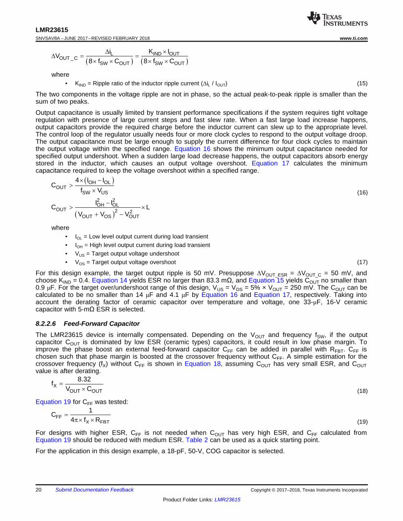
Output capacitance is usually limited by transient performance specifications if the system requires tight voltageregulation with presence of large current steps and fast slew rate. When a fast large load increase happens,output capacitors provide the required charge before the inductor current can slew up to the appropriate level.The control loop of the regulator usually needs four or more clock cycles to respond to the output voltage droop.The output capacitance must be large enough to supply the current difference for four clock cycles to maintainthe output voltage within the specified range. Equation 16 shows the minimum output capacitance needed forspecified output undershoot. When a sudden large load decrease happens, the output capacitors absorb energystored in the inductor, which causes an output voltage overshoot. Equation 17 calculates the minimumcapacitance required to keep the voltage overshoot within a specified range.
(16)
where• IOL = Low level output current during load transient• IOH = High level output current during load transient• VUS = Target output voltage undershoot• VOS = Target output voltage overshoot (17)
For this design example, the target output ripple is 50 mV. Presuppose ΔVOUT_ESR = ΔVOUT_C = 50 mV, andchoose KIND = 0.4. Equation 14 yields ESR no larger than 83.3 mΩ, and Equation 15 yields COUT no smaller than0.9 μF. For the target over/undershoot range of this design, VUS = VOS = 5% × VOUT = 250 mV. The COUT can becalculated to be no smaller than 14 μF and 4.1 μF by Equation 16 and Equation 17, respectively. Taking intoaccount the derating factor of ceramic capacitor over temperature and voltage, one 33-μF, 16-V ceramiccapacitor with 5-mΩ ESR is selected.
8.2.2.6 Feed-Forward CapacitorThe LMR23615 device is internally compensated. Depending on the VOUT and frequency fSW, if the outputcapacitor COUT is dominated by low ESR (ceramic types) capacitors, it could result in low phase margin. Toimprove the phase boost an external feed-forward capacitor CFF can be added in parallel with RFBT. CFF ischosen such that phase margin is boosted at the crossover frequency without CFF. A simple estimation for thecrossover frequency (fX) without CFF is shown in Equation 18, assuming COUT has very small ESR, and COUTvalue is after derating.
(18)
Equation 19 for CFF was tested:
(19)
For designs with higher ESR, CFF is not needed when COUT has very high ESR, and CFF calculated fromEquation 19 should be reduced with medium ESR. Table 2 can be used as a quick starting point.
For the application in this design example, a 18-pF, 50-V, COG capacitor is selected.

ENT ENBIN_FALLING ENH EN_HYS
ENB
R RV V V
R
u
IN_RISINGENT ENB
ENH
VR 1 R
V
§ · u¨ ¸¨ ¸© ¹
ENT ENBIN_RISING ENH
ENB
R RV V
R
u
21
LMR23615www.ti.com SNVSAV8A –JUNE 2017–REVISED FEBRUARY 2018
Product Folder Links: LMR23615
Submit Documentation FeedbackCopyright © 2017–2018, Texas Instruments Incorporated
8.2.2.7 Input Capacitor SelectionThe LMR23615 device requires high-frequency input decoupling capacitor(s) and a bulk input capacitor,depending on the application. The typical recommended value for the high-frequency decoupling capacitor is 4.7μF to 10 μF. TI recommends a high-quality ceramic capacitor type X5R or X7R with sufficiency voltage rating. Tocompensate the derating of ceramic capacitors, a voltage rating twice the maximum input voltage isrecommended. Additionally, some bulk capacitance can be required, especially if the LMR23615 circuit is notlocated within approximately 5 cm from the input voltage source. This capacitor is used to provide damping to thevoltage spike due to the lead inductance of the cable or the trace. For this design, two 4.7-μF, 50-V, X7R ceramiccapacitors are used. A 0.1-μF for high-frequency filtering and place it as close as possible to the device pins.
8.2.2.8 Bootstrap Capacitor SelectionEvery LMR23615 design requires a bootstrap capacitor (CBOOT). The recommended capacitor is 0.1 μF and rated16 V or higher. The bootstrap capacitor is located between the SW pin and the BOOT pin. The bootstrapcapacitor must be a high-quality ceramic type with an X7R or X5R grade dielectric for temperature stability.
8.2.2.9 VCC Capacitor SelectionThe VCC pin is the output of an internal LDO for the LMR23615 device. To insure stability of the device, place aminimum of 2.2-μF, 16-V, X7R capacitor from this pin to ground.
8.2.2.10 Undervoltage Lockout SetpointThe system undervoltage lockout (UVLO) is adjusted using the external voltage divider network of RENT andRENB. The UVLO has two thresholds, one for power up when the input voltage is rising and one for power downor brownouts when the input voltage is falling. Equation 20 can be used to determine the VIN UVLO level.
(20)
The EN rising threshold (VENH) for LMR23615 is set to be 1.55 V (typical). Choose the value of RENB to be 287kΩ to minimize input current from the supply. If the desired VIN UVLO level is at 6 V, then the value of RENT canbe calculated using Equation 21:
(21)
Equation 21 yields a value of 820 kΩ. The resulting falling UVLO threshold, equals 4.4 V, can be calculated byEquation 22, where EN hysteresis (VEN_HYS) is 0.4 V (typica).
(22)

22
LMR23615SNVSAV8A –JUNE 2017–REVISED FEBRUARY 2018 www.ti.com
Product Folder Links: LMR23615
Submit Documentation Feedback Copyright © 2017–2018, Texas Instruments Incorporated
8.2.3 Application CurvesUnless otherwise specified the following conditions apply: VIN = 12 V, fSW = 1600 kHz, L = 4.7 µH, COUT = 47 µF, TA = 25 °C.
VOUT = 5 V IOUT = 1.5 A fSW = 1600 kHz
Figure 23. CCM Mode
VOUT = 5 V IOUT = 0 mA fSW = 1600 kHz
Figure 24. PFM Mode
VIN = 12 V VOUT = 5 V IOUT = 1.5 A
Figure 25. Start-Up by VIN
VIN = 12 V VOUT = 5 V IOUT = 1.5 A
Figure 26. Start-Up by EN
VIN = 12 V VOUT = 5 VIOUT = 0.2 A to 1.5 A, 100 mA / μs
Figure 27. Load Transient
VIN = 7 V to 36 V, 2 V / μs IOUT = 1.5 AVOUT = 5 V
Figure 28. Line Transient

23
LMR23615www.ti.com SNVSAV8A –JUNE 2017–REVISED FEBRUARY 2018
Product Folder Links: LMR23615
Submit Documentation FeedbackCopyright © 2017–2018, Texas Instruments Incorporated
Unless otherwise specified the following conditions apply: VIN = 12 V, fSW = 1600 kHz, L = 4.7 µH, COUT = 47 µF, TA = 25 °C.
VOUT = 5 V IOUT = 1 A to short
Figure 29. Short Protection
VOUT = 5 V IOUT = short to 1 A
Figure 30. Short Recovery
9 Power Supply RecommendationsThe LMR23615 is designed to operate from an input voltage supply range between 4 V and 36 V. This inputsupply must be able to withstand the maximum input current and maintain a stable voltage. The resistance of theinput supply rail must be low enough that an input current transient does not cause a high enough drop at theLMR23615 supply voltage that can cause a false UVLO fault triggering and system reset. If the input supply islocated more than a few inches from the LMR23615, additional bulk capacitance may be required in addition tothe ceramic input capacitors. The amount of bulk capacitance is not critical, but a 47-μF or 100-μF electrolyticcapacitor is a typical choice.
24
LMR23615SNVSAV8A –JUNE 2017–REVISED FEBRUARY 2018 www.ti.com
Product Folder Links: LMR23615
Submit Documentation Feedback Copyright © 2017–2018, Texas Instruments Incorporated
10 Layout
10.1 Layout GuidelinesLayout is a critical portion of good power supply design. The following guidelines will help users design a PCBwith the best power-conversion performance, thermal performance, and minimized generation of unwanted EMI.1. The input bypass capacitor CIN must be placed as close as possible to the VIN and PGND pins. Grounding
for both the input and output capacitors should consist of localized top side planes that connect to the PGNDpin and PAD.
2. Place bypass capacitors for VCC close to the VCC pin and ground the bypass capacitor to device ground.3. Minimize trace length to the FB pin net. Both feedback resistors, RFBT and RFBB must be located close to the
FB pin. Place CFF directly in parallel with RFBT. If VOUT accuracy at the load is important, ensure that the VOUTsense is made at the load. Route VOUT sense path away from noisy nodes and preferably through a layer onthe other side of a shielded layer.
4. Use ground plane in one of the middle layers as noise shielding and heat dissipation path.5. Have a single point ground connection to the plane. Route the ground connections for the feedback and
enable components to the ground plane. This prevents any switched or load currents from flowing in theanalog ground traces. If not properly handled, poor grounding can result in degraded load regulation orerratic output voltage ripple behavior.
6. Make VIN, VOUT and ground bus connections as wide as possible. This reduces any voltage drops on theinput or output paths of the converter and maximizes efficiency.
7. Provide adequate device heat sinking. Use an array of heat-sinking vias to connect the exposed pad to theground plane on the bottom PCB layer. If the PCB has multiple copper layers, these thermal vias can also beconnected to inner layer heat-spreading ground planes. Ensure enough copper area is used for heat sinkingto keep the junction temperature below 125°C.
10.1.1 Compact Layout for EMI ReductionRadiated EMI is generated by the high di/dt components in pulsing currents in switching converters. The largerarea covered by the path of a pulsing current, the more EMI is generated. High frequency ceramic bypasscapacitors at the input side provide primary path for the high di/dt components of the pulsing current. Placingceramic bypass capacitor(s) as close as possible to the VIN and PGND pins is the key to EMI reduction.
The SW pin connecting to the inductor must be as short as possible, and just wide enough to carry the loadcurrent without excessive heating. Use short, thick traces or copper pours (shapes) for high-current conductionpath to minimize parasitic resistance. The output capacitors must be placed close to the VOUT end of the inductorand closely grounded to PGND pin and exposed PAD.
Place the bypass capacitors on VCC as close as possible to the pin and closely grounded to PGND and theexposed PAD.
10.1.2 Ground Plane and Thermal ConsiderationsTI recommends using one of the middle layers as a solid ground plane. Ground plane provides shielding forsensitive circuits and traces. It also provides a quiet reference potential for the control circuitry. Connect theAGND and PGND pins to the ground plane using vias right next to the bypass capacitors. PGND pin isconnected to the source of the internal LS switch. They must be connected directly to the grounds of the inputand output capacitors. The PGND net contains noise at switching frequency and may bounce due to loadvariations. PGND trace, as well as VIN and SW traces, must be constrained to one side of the ground plane. Theother side of the ground plane contains much less noise and should be used for sensitive routes.
TI recommends providing adequate device heat sinking by utilizing the PAD of the device as the primary thermalpath. Use a minimum 4 by 2 array of 12 mil thermal vias to connect the PAD to the system ground plane heatsink. The vias should be evenly distributed under the PAD. Use as much copper as possible, for system groundplane, on the top and bottom layers for the best heat dissipation. Use a four-layer board with the copperthickness for the four layers, starting from the top of, 2 oz / 1 oz / 1 oz / 2 oz. Four-layer boards with enoughcopper thickness provides low current conduction impedance, proper shielding, and lower thermal resistance.

25
LMR23615www.ti.com SNVSAV8A –JUNE 2017–REVISED FEBRUARY 2018
Product Folder Links: LMR23615
Submit Documentation FeedbackCopyright © 2017–2018, Texas Instruments Incorporated
Layout Guidelines (continued)The thermal characteristics of the LMR23615 are specified using the parameter RθJA, which characterize thejunction temperature of silicon to the ambient temperature in a specific system. Although the value of RθJA isdependent on many variables, it still can be used to approximate the operating junction temperature of thedevice. To obtain an estimate of the device junction temperature, one may use the following relationship:
TJ = PD × RθJA + TA (23)PD = VIN x IIN × (1 – Efficiency) – 1.1 × IOUT
2 × DCR in watt
where• TJ = junction temperature in °C• PD = device power dissipation in watt• RθJA = junction-to-ambient thermal resistance of the device in °C/W• TA = ambient temperature in °C• DCR = inductor DC parasitic resistance in ohm (24)
The recommended operating junction temperature of the LMR23615 is 125°C. RθJA is highly related to PCB sizeand layout, as well as environmental factors such as heat sinking and air flow.
10.1.3 Feedback ResistorsTo reduce noise sensitivity of the output voltage feedback path, it is important to place the resistor divider andCFF close to the FB pin, rather than close to the load. The FB pin is the input to the error amplifier, so it is a highimpedance node and very sensitive to noise. Placing the resistor divider and CFF closer to the FB pin reduces thetrace length of FB signal and reduces noise coupling. The output node is a low impedance node, so the tracefrom VOUT to the resistor divider can be long if short path is not available.
If voltage accuracy at the load is important, make sure voltage sense is made at the load. Doing so corrects forvoltage drops along the traces and provide the best output accuracy. Route the voltage sense trace from theload to the feedback resistor divider away from the SW node path and the inductor to avoid contaminating thefeedback signal with switch noise, while also minimizing the trace length. This is most important when high-valueresistors are used to set the output voltage. TI recommends routing the voltage sense trace and place theresistor divider on a different layer than the inductor and SW node path, such that there is a ground plane inbetween the feedback trace and inductor/SW node polygon. This provides further shielding for the voltagefeedback path from EMI noises.
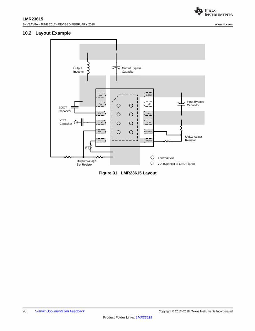
UVLO Adjust Resistor
Input Bypass Capacitor
Output Bypass Capacitor
BOOT Capacitor
Thermal VIA
VIA (Connect to GND Plane)
Output Inductor
Output Voltage Set Resistor
VCCCapacitor
SW
SW
BOOT
VCC
FB
RT
PGND
NC
VIN
VIN
EN/SYNC
AGND
RT
26
LMR23615SNVSAV8A –JUNE 2017–REVISED FEBRUARY 2018 www.ti.com
Product Folder Links: LMR23615
Submit Documentation Feedback Copyright © 2017–2018, Texas Instruments Incorporated
10.2 Layout Example
Figure 31. LMR23615 Layout

27
LMR23615www.ti.com SNVSAV8A –JUNE 2017–REVISED FEBRUARY 2018
Product Folder Links: LMR23615
Submit Documentation FeedbackCopyright © 2017–2018, Texas Instruments Incorporated
11 Device and Documentation Support
11.1 Device Support
11.1.1 Development Support
11.1.1.1 Custom Design With WEBENCH® ToolsClick here to create a custom design using the LMR23615 device with the WEBENCH® Power Designer.1. Start by entering the input voltage (VIN), output voltage (VOUT), and output current (IOUT) requirements.2. Optimize the design for key parameters such as efficiency, footprint, and cost using the optimizer dial.3. Compare the generated design with other possible solutions from Texas Instruments.
The WEBENCH Power Designer provides a customized schematic along with a list of materials with real-timepricing and component availability.
In most cases, these actions are available:• Run electrical simulations to see important waveforms and circuit performance• Run thermal simulations to understand board thermal performance• Export customized schematic and layout into popular CAD formats• Print PDF reports for the design, and share the design with colleagues
Get more information about WEBENCH tools at www.ti.com/WEBENCH.
11.2 Receiving Notification of Documentation UpdatesTo receive notification of documentation updates, navigate to the device product folder on ti.com. In the upperright corner, click on Alert me to register and receive a weekly digest of any product information that haschanged. For change details, review the revision history included in any revised document.
11.3 Community ResourcesThe following links connect to TI community resources. Linked contents are provided "AS IS" by the respectivecontributors. They do not constitute TI specifications and do not necessarily reflect TI's views; see TI's Terms ofUse.
TI E2E™ Online Community TI's Engineer-to-Engineer (E2E) Community. Created to foster collaborationamong engineers. At e2e.ti.com, you can ask questions, share knowledge, explore ideas and helpsolve problems with fellow engineers.
Design Support TI's Design Support Quickly find helpful E2E forums along with design support tools andcontact information for technical support.
11.4 TrademarksPowerPAD, E2E are trademarks of Texas Instruments.WEBENCH, SIMPLE SWITCHER are registered trademarks of Texas Instruments.All other trademarks are the property of their respective owners.
11.5 Electrostatic Discharge CautionThese devices have limited built-in ESD protection. The leads should be shorted together or the device placed in conductive foamduring storage or handling to prevent electrostatic damage to the MOS gates.
11.6 GlossarySLYZ022 — TI Glossary.
This glossary lists and explains terms, acronyms, and definitions.

28
LMR23615SNVSAV8A –JUNE 2017–REVISED FEBRUARY 2018 www.ti.com
Product Folder Links: LMR23615
Submit Documentation Feedback Copyright © 2017–2018, Texas Instruments Incorporated
12 Mechanical, Packaging, and Orderable InformationThe following pages include mechanical, packaging, and orderable information. This information is the mostcurrent data available for the designated devices. This data is subject to change without notice and revision ofthis document. For browser-based versions of this data sheet, refer to the left-hand navigation.
PACKAGE OPTION ADDENDUM
www.ti.com 12-Mar-2018
Addendum-Page 1
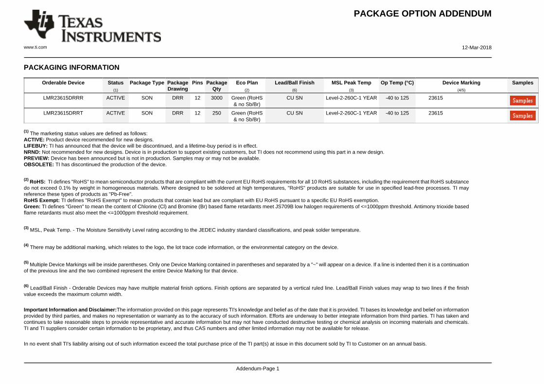
PACKAGING INFORMATION
Orderable Device Status(1)
Package Type PackageDrawing
Pins PackageQty
Eco Plan(2)
Lead/Ball Finish(6)
MSL Peak Temp(3)
Op Temp (°C) Device Marking(4/5)
Samples
LMR23615DRRR ACTIVE SON DRR 12 3000 Green (RoHS& no Sb/Br)
CU SN Level-2-260C-1 YEAR -40 to 125 23615
LMR23615DRRT ACTIVE SON DRR 12 250 Green (RoHS& no Sb/Br)
CU SN Level-2-260C-1 YEAR -40 to 125 23615
(1) The marketing status values are defined as follows:ACTIVE: Product device recommended for new designs.LIFEBUY: TI has announced that the device will be discontinued, and a lifetime-buy period is in effect.NRND: Not recommended for new designs. Device is in production to support existing customers, but TI does not recommend using this part in a new design.PREVIEW: Device has been announced but is not in production. Samples may or may not be available.OBSOLETE: TI has discontinued the production of the device.
(2) RoHS: TI defines "RoHS" to mean semiconductor products that are compliant with the current EU RoHS requirements for all 10 RoHS substances, including the requirement that RoHS substancedo not exceed 0.1% by weight in homogeneous materials. Where designed to be soldered at high temperatures, "RoHS" products are suitable for use in specified lead-free processes. TI mayreference these types of products as "Pb-Free".RoHS Exempt: TI defines "RoHS Exempt" to mean products that contain lead but are compliant with EU RoHS pursuant to a specific EU RoHS exemption.Green: TI defines "Green" to mean the content of Chlorine (Cl) and Bromine (Br) based flame retardants meet JS709B low halogen requirements of <=1000ppm threshold. Antimony trioxide basedflame retardants must also meet the <=1000ppm threshold requirement.
(3) MSL, Peak Temp. - The Moisture Sensitivity Level rating according to the JEDEC industry standard classifications, and peak solder temperature.
(4) There may be additional marking, which relates to the logo, the lot trace code information, or the environmental category on the device.
(5) Multiple Device Markings will be inside parentheses. Only one Device Marking contained in parentheses and separated by a "~" will appear on a device. If a line is indented then it is a continuationof the previous line and the two combined represent the entire Device Marking for that device.
(6) Lead/Ball Finish - Orderable Devices may have multiple material finish options. Finish options are separated by a vertical ruled line. Lead/Ball Finish values may wrap to two lines if the finishvalue exceeds the maximum column width.
Important Information and Disclaimer:The information provided on this page represents TI's knowledge and belief as of the date that it is provided. TI bases its knowledge and belief on informationprovided by third parties, and makes no representation or warranty as to the accuracy of such information. Efforts are underway to better integrate information from third parties. TI has taken andcontinues to take reasonable steps to provide representative and accurate information but may not have conducted destructive testing or chemical analysis on incoming materials and chemicals.TI and TI suppliers consider certain information to be proprietary, and thus CAS numbers and other limited information may not be available for release.
In no event shall TI's liability arising out of such information exceed the total purchase price of the TI part(s) at issue in this document sold by TI to Customer on an annual basis.
PACKAGE OPTION ADDENDUM
www.ti.com 12-Mar-2018
Addendum-Page 2
OTHER QUALIFIED VERSIONS OF LMR23615 :
• Automotive: LMR23615-Q1
NOTE: Qualified Version Definitions:
• Automotive - Q100 devices qualified for high-reliability automotive applications targeting zero defects
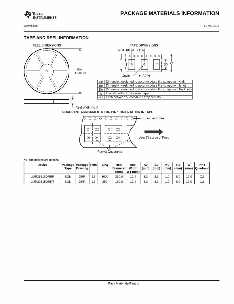
TAPE AND REEL INFORMATION
*All dimensions are nominal
Device PackageType
PackageDrawing
Pins SPQ ReelDiameter
(mm)
ReelWidth
W1 (mm)
A0(mm)
B0(mm)
K0(mm)
P1(mm)
W(mm)
Pin1Quadrant
LMR23615DRRR SON DRR 12 3000 330.0 12.4 3.3 3.3 1.0 8.0 12.0 Q2
LMR23615DRRT SON DRR 12 250 180.0 12.4 3.3 3.3 1.0 8.0 12.0 Q2
PACKAGE MATERIALS INFORMATION
www.ti.com 11-Mar-2018
Pack Materials-Page 1
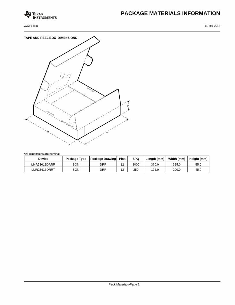
*All dimensions are nominal
Device Package Type Package Drawing Pins SPQ Length (mm) Width (mm) Height (mm)
LMR23615DRRR SON DRR 12 3000 370.0 355.0 55.0
LMR23615DRRT SON DRR 12 250 195.0 200.0 45.0
PACKAGE MATERIALS INFORMATION
www.ti.com 11-Mar-2018
Pack Materials-Page 2

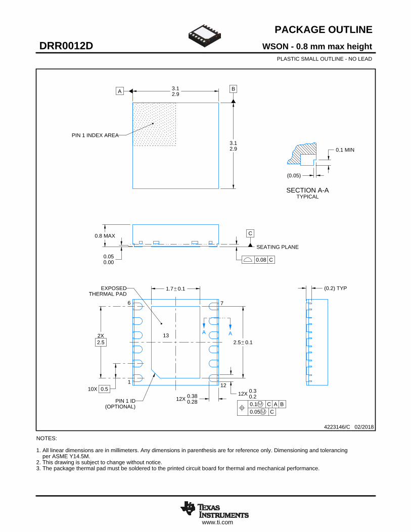
A A
www.ti.com
PACKAGE OUTLINE
C
12X 0.30.2
2.5 0.12X2.5
1.7 0.1
10X 0.5
0.8 MAX
12X 0.380.28
0.050.00
A 3.12.9
B
3.12.9
(0.2) TYP
0.1 MIN
(0.05)
WSON - 0.8 mm max heightDRR0012DPLASTIC SMALL OUTLINE - NO LEAD
4223146/C 02/2018
PIN 1 INDEX AREA
SEATING PLANE
0.08 C
1
6 7
12
(OPTIONAL)PIN 1 ID 0.1 C A B
0.05 C
THERMAL PADEXPOSED
13
NOTES: 1. All linear dimensions are in millimeters. Any dimensions in parenthesis are for reference only. Dimensioning and tolerancing per ASME Y14.5M. 2. This drawing is subject to change without notice. 3. The package thermal pad must be soldered to the printed circuit board for thermal and mechanical performance.
SCALE 4.000
SCALE 30.000SECTION A-A
SECTION A-ATYPICAL

www.ti.com
EXAMPLE BOARD LAYOUT
0.07 MINALL AROUND
0.07 MAXALL AROUND
12X (0.25)
(2.5)
(2.87)
10X (0.5)
(1.7)
( 0.2) VIATYP
(0.6)
(1)
12X (0.53)
(R0.05) TYP
WSON - 0.8 mm max heightDRR0012DPLASTIC SMALL OUTLINE - NO LEAD
4223146/C 02/2018
SYMM1
6 7
12
LAND PATTERN EXAMPLEEXPOSED METAL SHOWN
SCALE:20X
13
NOTES: (continued) 4. This package is designed to be soldered to a thermal pad on the board. For more information, see Texas Instruments literature number SLUA271 (www.ti.com/lit/slua271).5. Vias are optional depending on application, refer to device data sheet. If any vias are implemented, refer to their locations shown on this view. It is recommended that vias under paste be filled, plugged or tented.
SYMM
SOLDER MASKOPENINGSOLDER MASK
METAL UNDER
SOLDER MASKDEFINED
EXPOSED METAL
METAL EDGESOLDER MASKOPENING
SOLDER MASK DETAILS
NON SOLDER MASKDEFINED
(PREFERRED)
EXPOSED METAL
www.ti.com
EXAMPLE STENCIL DESIGN
(R0.05) TYP
12X (0.25)
12X (0.53)
(0.74)
(1.15)
(2.87)
(0.675)
10X (0.5)
(0.47)
WSON - 0.8 mm max heightDRR0012DPLASTIC SMALL OUTLINE - NO LEAD
4223146/C 02/2018
NOTES: (continued) 6. Laser cutting apertures with trapezoidal walls and rounded corners may offer better paste release. IPC-7525 may have alternate design recommendations.
SOLDER PASTE EXAMPLEBASED ON 0.125 mm THICK STENCIL
EXPOSED PAD
80.1% PRINTED SOLDER COVERAGE BY AREASCALE:25X
SYMM
1
6 7
12
METALTYP
SYMM13
IMPORTANT NOTICE
Texas Instruments Incorporated (TI) reserves the right to make corrections, enhancements, improvements and other changes to itssemiconductor products and services per JESD46, latest issue, and to discontinue any product or service per JESD48, latest issue. Buyersshould obtain the latest relevant information before placing orders and should verify that such information is current and complete.TI’s published terms of sale for semiconductor products (http://www.ti.com/sc/docs/stdterms.htm) apply to the sale of packaged integratedcircuit products that TI has qualified and released to market. Additional terms may apply to the use or sale of other types of TI products andservices.Reproduction of significant portions of TI information in TI data sheets is permissible only if reproduction is without alteration and isaccompanied by all associated warranties, conditions, limitations, and notices. TI is not responsible or liable for such reproduceddocumentation. Information of third parties may be subject to additional restrictions. Resale of TI products or services with statementsdifferent from or beyond the parameters stated by TI for that product or service voids all express and any implied warranties for theassociated TI product or service and is an unfair and deceptive business practice. TI is not responsible or liable for any such statements.Buyers and others who are developing systems that incorporate TI products (collectively, “Designers”) understand and agree that Designersremain responsible for using their independent analysis, evaluation and judgment in designing their applications and that Designers havefull and exclusive responsibility to assure the safety of Designers' applications and compliance of their applications (and of all TI productsused in or for Designers’ applications) with all applicable regulations, laws and other applicable requirements. Designer represents that, withrespect to their applications, Designer has all the necessary expertise to create and implement safeguards that (1) anticipate dangerousconsequences of failures, (2) monitor failures and their consequences, and (3) lessen the likelihood of failures that might cause harm andtake appropriate actions. Designer agrees that prior to using or distributing any applications that include TI products, Designer willthoroughly test such applications and the functionality of such TI products as used in such applications.TI’s provision of technical, application or other design advice, quality characterization, reliability data or other services or information,including, but not limited to, reference designs and materials relating to evaluation modules, (collectively, “TI Resources”) are intended toassist designers who are developing applications that incorporate TI products; by downloading, accessing or using TI Resources in anyway, Designer (individually or, if Designer is acting on behalf of a company, Designer’s company) agrees to use any particular TI Resourcesolely for this purpose and subject to the terms of this Notice.TI’s provision of TI Resources does not expand or otherwise alter TI’s applicable published warranties or warranty disclaimers for TIproducts, and no additional obligations or liabilities arise from TI providing such TI Resources. TI reserves the right to make corrections,enhancements, improvements and other changes to its TI Resources. TI has not conducted any testing other than that specificallydescribed in the published documentation for a particular TI Resource.Designer is authorized to use, copy and modify any individual TI Resource only in connection with the development of applications thatinclude the TI product(s) identified in such TI Resource. NO OTHER LICENSE, EXPRESS OR IMPLIED, BY ESTOPPEL OR OTHERWISETO ANY OTHER TI INTELLECTUAL PROPERTY RIGHT, AND NO LICENSE TO ANY TECHNOLOGY OR INTELLECTUAL PROPERTYRIGHT OF TI OR ANY THIRD PARTY IS GRANTED HEREIN, including but not limited to any patent right, copyright, mask work right, orother intellectual property right relating to any combination, machine, or process in which TI products or services are used. Informationregarding or referencing third-party products or services does not constitute a license to use such products or services, or a warranty orendorsement thereof. Use of TI Resources may require a license from a third party under the patents or other intellectual property of thethird party, or a license from TI under the patents or other intellectual property of TI.TI RESOURCES ARE PROVIDED “AS IS” AND WITH ALL FAULTS. TI DISCLAIMS ALL OTHER WARRANTIES ORREPRESENTATIONS, EXPRESS OR IMPLIED, REGARDING RESOURCES OR USE THEREOF, INCLUDING BUT NOT LIMITED TOACCURACY OR COMPLETENESS, TITLE, ANY EPIDEMIC FAILURE WARRANTY AND ANY IMPLIED WARRANTIES OFMERCHANTABILITY, FITNESS FOR A PARTICULAR PURPOSE, AND NON-INFRINGEMENT OF ANY THIRD PARTY INTELLECTUALPROPERTY RIGHTS. TI SHALL NOT BE LIABLE FOR AND SHALL NOT DEFEND OR INDEMNIFY DESIGNER AGAINST ANY CLAIM,INCLUDING BUT NOT LIMITED TO ANY INFRINGEMENT CLAIM THAT RELATES TO OR IS BASED ON ANY COMBINATION OFPRODUCTS EVEN IF DESCRIBED IN TI RESOURCES OR OTHERWISE. IN NO EVENT SHALL TI BE LIABLE FOR ANY ACTUAL,DIRECT, SPECIAL, COLLATERAL, INDIRECT, PUNITIVE, INCIDENTAL, CONSEQUENTIAL OR EXEMPLARY DAMAGES INCONNECTION WITH OR ARISING OUT OF TI RESOURCES OR USE THEREOF, AND REGARDLESS OF WHETHER TI HAS BEENADVISED OF THE POSSIBILITY OF SUCH DAMAGES.Unless TI has explicitly designated an individual product as meeting the requirements of a particular industry standard (e.g., ISO/TS 16949and ISO 26262), TI is not responsible for any failure to meet such industry standard requirements.Where TI specifically promotes products as facilitating functional safety or as compliant with industry functional safety standards, suchproducts are intended to help enable customers to design and create their own applications that meet applicable functional safety standardsand requirements. Using products in an application does not by itself establish any safety features in the application. Designers mustensure compliance with safety-related requirements and standards applicable to their applications. Designer may not use any TI products inlife-critical medical equipment unless authorized officers of the parties have executed a special contract specifically governing such use.Life-critical medical equipment is medical equipment where failure of such equipment would cause serious bodily injury or death (e.g., lifesupport, pacemakers, defibrillators, heart pumps, neurostimulators, and implantables). Such equipment includes, without limitation, allmedical devices identified by the U.S. Food and Drug Administration as Class III devices and equivalent classifications outside the U.S.TI may expressly designate certain products as completing a particular qualification (e.g., Q100, Military Grade, or Enhanced Product).Designers agree that it has the necessary expertise to select the product with the appropriate qualification designation for their applicationsand that proper product selection is at Designers’ own risk. Designers are solely responsible for compliance with all legal and regulatoryrequirements in connection with such selection.Designer will fully indemnify TI and its representatives against any damages, costs, losses, and/or liabilities arising out of Designer’s non-compliance with the terms and provisions of this Notice.
Mailing Address: Texas Instruments, Post Office Box 655303, Dallas, Texas 75265Copyright © 2018, Texas Instruments Incorporated