Embed Size (px)
Citation preview
28 mar 2010
2nd generation ASICs
for CALICE/EUDET
C. de LA TAILLE
28 mar 2010 CdLT : ASIC developments in CALICE/EUDET LCWS 2010 2
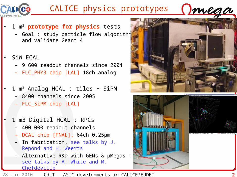
• 1 m3 prototype for physics tests– Goal : study particle flow algorithm and
validate Geant 4
• SiW ECAL– 9 600 readout channels since 2004– FLC_PHY3 chip [LAL] 18ch analog
• 1 m3 Analog HCAL : tiles + SiPM– 8400 channels since 2005– FLC_SiPM chip [LAL]
• 1 m3 Digital HCAL : RPCs– 400 000 readout channels– DCAL chip [FNAL], 64ch 0.25µm– In fabrication, see talks by J. Repond and
H. Weerts– Alternative R&D with GEMs & µMegas :
see talks by A. White and M. Chefdeville
CALICE physics prototypes
28 mar 2010 CdLT : ASIC developments in CALICE/EUDET LCWS 2010 3
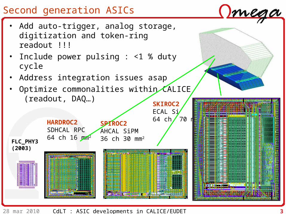
Second generation ASICs
• Add auto-trigger, analog storage, digitization and token-ring readout !!!
• Include power pulsing : <1 % duty cycle• Address integration issues asap• Optimize commonalities within CALICE
(readout, DAQ…)
FLC_PHY3(2003)
SPIROCAnalog HCAL(SiPM)36 ch. 32mm²June 07
HARDROC2SDHCAL RPC64 ch 16 mm2
SKIROC2ECAL Si64 ch. 70 mm2
SPIROC2AHCAL SiPM36 ch 30 mm2
28 mar 2010 CdLT : ASIC developments in CALICE/EUDET LCWS 2010 4
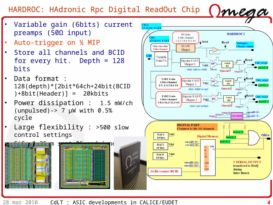
HARDROC: HAdronic Rpc Digital ReadOut Chip
• Variable gain (6bits) current preamps (50Ω input)
• Auto-trigger on ½ MIP• Store all channels and BCID for
every hit. Depth = 128 bits• Data format :
128(depth)*[2bit*64ch+24bit(BCID)+8bit(Header)] = 20kbits
• Power dissipation : 1.5 mW/ch (unpulsed)-> 7 µW with 0.5% cycle
• Large flexibility : >500 slow control settings
• SiGe 0.35µm sept 06 and june 08
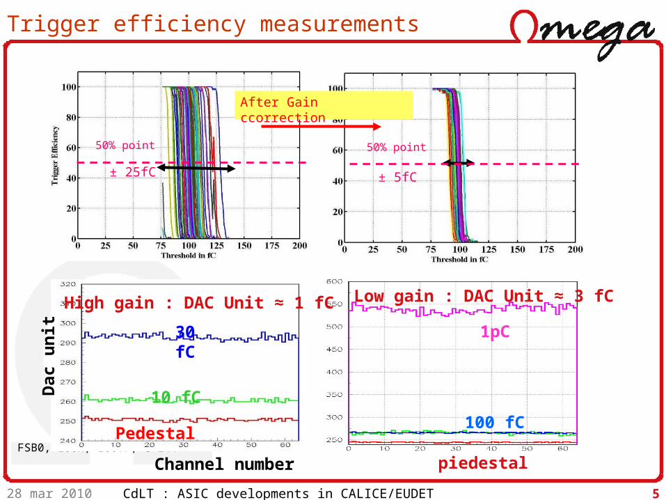
28 mar 2010 CdLT : ASIC developments in CALICE/EUDET LCWS 2010 5
Trigger efficiency measurements
FSB0, 100K, 100fF, G=144
After Gain ccorrection
50% point
± 5fC± 25fC
50% point
30 fC
10 fC
Pedestal
Dac
un
it
Channel number
1pC
100 fC
piedestal
Low gain : DAC Unit ≈ 3 fC High gain : DAC Unit ≈ 1 fC
28 mar 2010 CdLT : ASIC developments in CALICE/EUDET LCWS 2010 6
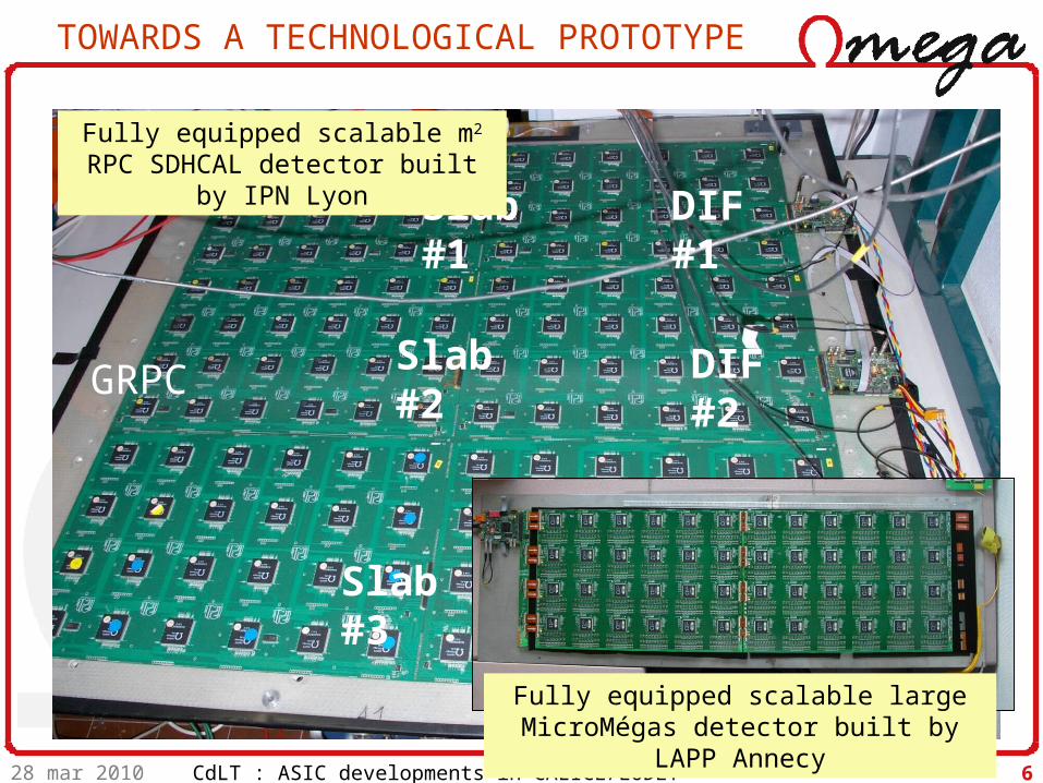
Slab #1
Slab #2
Slab #3
DIF #1
DIF #2
DIF #3
GRPC
TOWARDS A TECHNOLOGICAL PROTOTYPE
Fully equipped scalable m2 RPC SDHCAL detector built by IPN Lyon
Fully equipped scalable large MicroMégas detector built by LAPP Annecy
28 mar 2010 CdLT : ASIC developments in CALICE/EUDET LCWS 2010 7
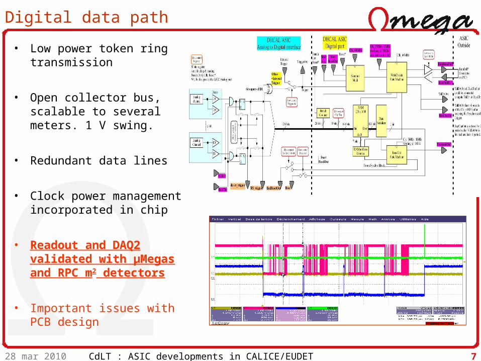
Digital data path
• Low power token ring transmission
• Open collector bus, scalable to several meters. 1 V swing.
• Redundant data lines
• Clock power management incorporated in chip
• Readout and DAQ2 validated with µMegas and RPC m2 detectors
• Important issues with PCB design
C. Combaret Calice week at UT Arlington, march 2010
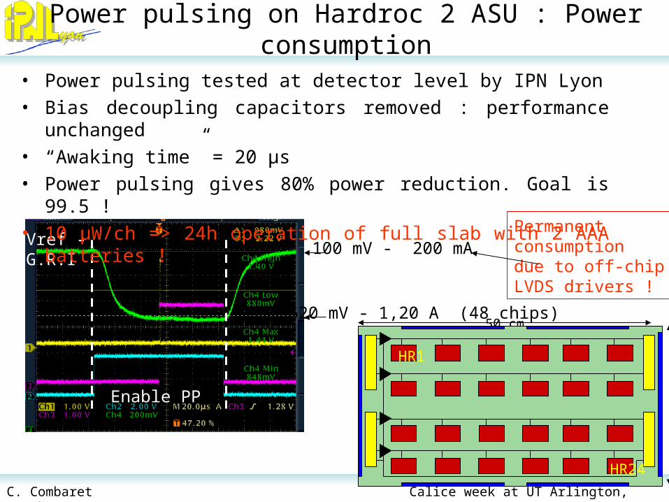
Power pulsing on Hardroc 2 ASU : Power consumption
Enable PP
Vref -G.R.I 100 mV - 200 mA
620 mV - 1,20 A (48 chips)
Permanent consumptiondue to off-chip LVDS drivers !
• Power pulsing tested at detector level by IPN Lyon• Bias decoupling capacitors removed : performance unchanged• “Awaking time” = 20 µs• Power pulsing gives 80% power reduction. Goal is 99.5 !• 10 µW/ch => 24h operation of full slab with 2 AAA batteries !
50 cm
HR1
HR24
28 mar 2010 CdLT : ASIC developments in CALICE/EUDET LCWS 2010 9
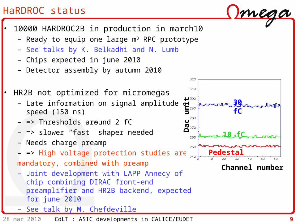
HaRDROC status
• 10000 HARDROC2B in production in march10 – Ready to equip one large m3 RPC prototype– See talks by K. Belkadhi and N. Lumb– Chips expected in june 2010– Detector assembly by autumn 2010
• HR2B not optimized for micromegas– Late information on signal amplitude and
speed (150 ns)– => Thresholds around 2 fC– => slower “fast” shaper needed– Needs charge preamp– => High voltage protection studies are mandatory, combined with preamp– Joint development with LAPP Annecy of chip
combining DIRAC front-end preamplifier and HR2B backend, expected for june 2010
– See talk by M. Chefdeville
30 fC
10 fC
Pedestal
Dac
un
it
Channel number
28 mar 2010 CdLT : ASIC developments in CALICE/EUDET LCWS 2010 10
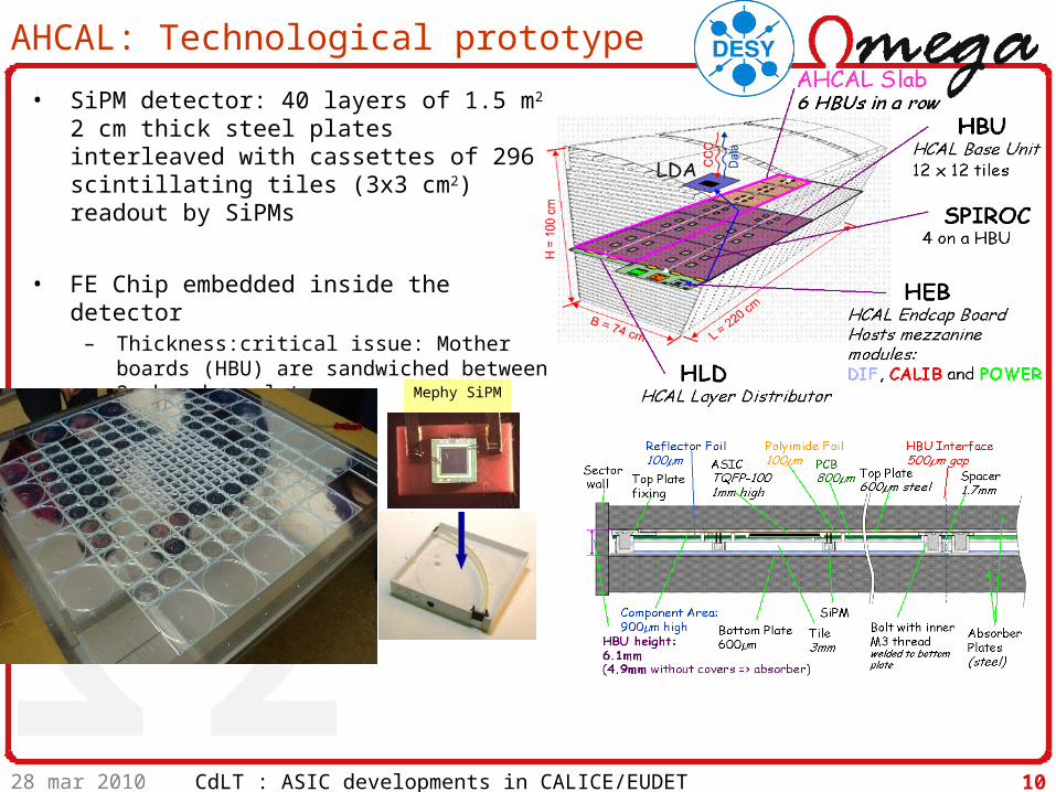
AHCAL: Technological prototype
• SiPM detector: 40 layers of 1.5 m2 2 cm thick steel plates interleaved with cassettes of 296 scintillating tiles (3x3 cm2) readout by SiPMs
• FE Chip embedded inside the detector– Thickness:critical issue: Mother boards
(HBU) are sandwiched between 2 absorber plates
Mephy SiPM
28 mar 2010 CdLT : ASIC developments in CALICE/EUDET LCWS 2010 11
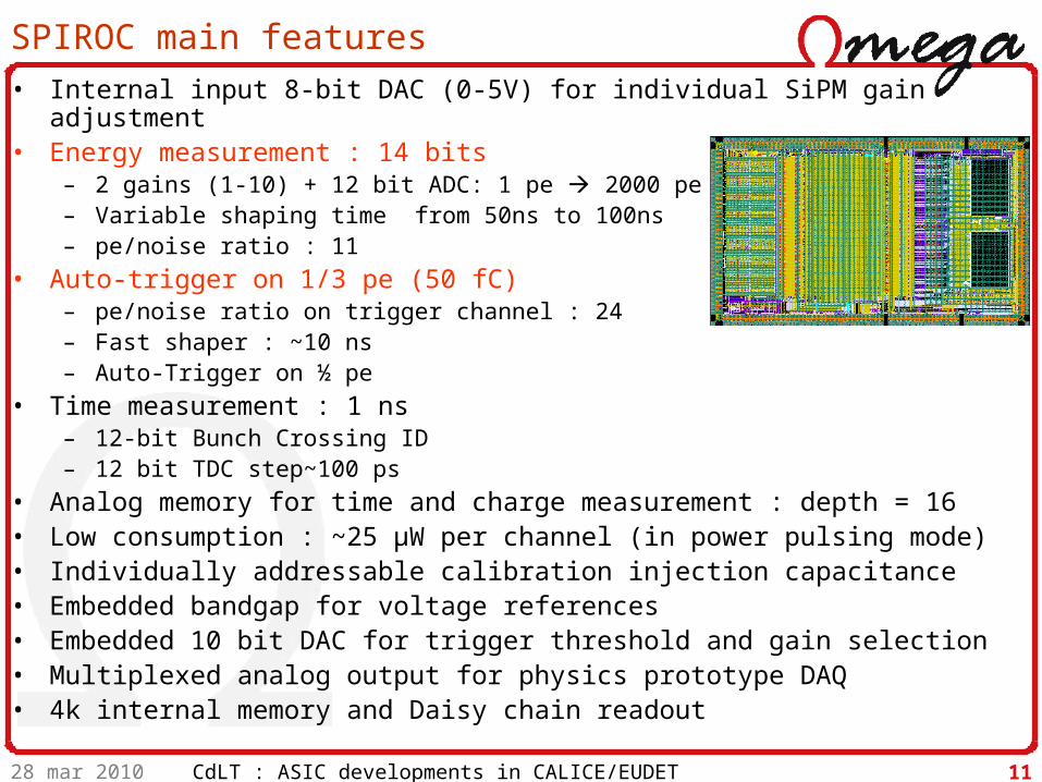
SPIROC main features• Internal input 8-bit DAC (0-5V) for individual SiPM gain adjustment• Energy measurement : 14 bits
– 2 gains (1-10) + 12 bit ADC: 1 pe 2000 pe– Variable shaping time from 50ns to 100ns – pe/noise ratio : 11
• Auto-trigger on 1/3 pe (50 fC)– pe/noise ratio on trigger channel : 24– Fast shaper : ~10 ns– Auto-Trigger on ½ pe
• Time measurement : 1 ns– 12-bit Bunch Crossing ID– 12 bit TDC step~100 ps
• Analog memory for time and charge measurement : depth = 16• Low consumption : ~25 µW per channel (in power pulsing mode)• Individually addressable calibration injection capacitance• Embedded bandgap for voltage references• Embedded 10 bit DAC for trigger threshold and gain selection• Multiplexed analog output for physics prototype DAQ• 4k internal memory and Daisy chain readout
28 mar 2010 CdLT : ASIC developments in CALICE/EUDET LCWS 2010 12
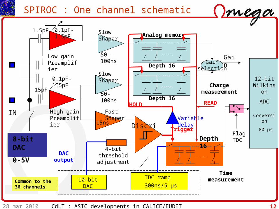
SPIROC : One channel schematic
50 -100ns
50-100ns
Gain selection
4-bit threshold adjustment
10-bit DAC
15ns
DAC output
HOLD
Slow Shaper
Slow Shaper
Fast Shaper
Time measurement
Charge measurement
TDC ramp
300ns/5 µs
12-bit Wilkinson
ADC
Trigger
Depth 16
Depth 16
Depth 16
Common to the 36 channels
8-bit DAC
0-5V
Low gain Preamplifier
High gain Preamplifier
Analog memory
15pF
1.5pF
0.1pF-1.5pF
Conversion
80 µs
READ
Variable delay
0.1pF-1.5pF
IN
Discri
Gain
Flag TDC
28 mar 2010 CdLT : ASIC developments in CALICE/EUDET LCWS 2010 13
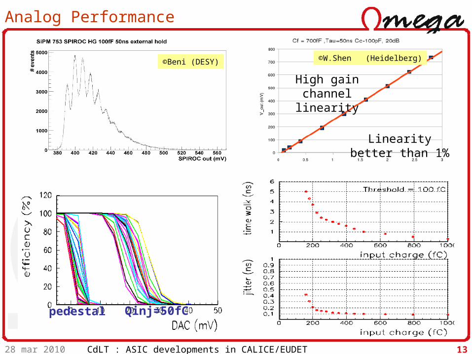
Analog Performance
pedestal Qinj=50fC
High gain channel linearity
Linearity better than 1%
©W.Shen (Heidelberg)©Beni (DESY)
28 mar 2010 CdLT : ASIC developments in CALICE/EUDET LCWS 2010 14
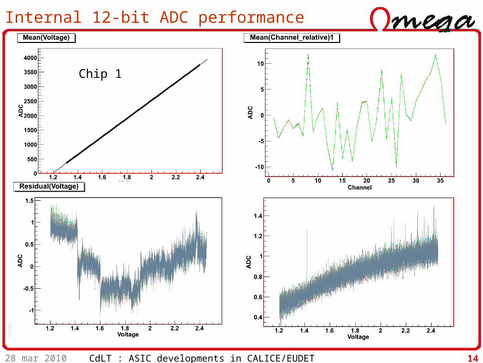
Internal 12-bit ADC performance
Chip 1
28 mar 2010 CdLT : ASIC developments in CALICE/EUDET LCWS 2010 15
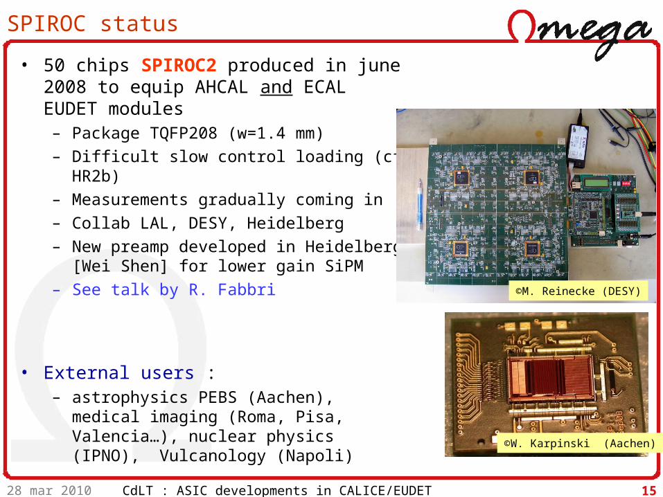
SPIROC status
• 50 chips SPIROC2 produced in june 2008 to equip AHCAL and ECAL EUDET modules– Package TQFP208 (w=1.4 mm)– Difficult slow control loading (cf HR2b)– Measurements gradually coming in– Collab LAL, DESY, Heidelberg– New preamp developed in Heidelberg
[Wei Shen] for lower gain SiPM– See talk by R. Fabbri
• External users : – astrophysics PEBS (Aachen), medical
imaging (Roma, Pisa, Valencia…), nuclear physics (IPNO), Vulcanology (Napoli) ©W. Karpinski (Aachen)
©M. Reinecke (DESY)
Mathias Reinecke | HCAL main meeting - Hamburg | Dec. 10th, 2009 | Page 16
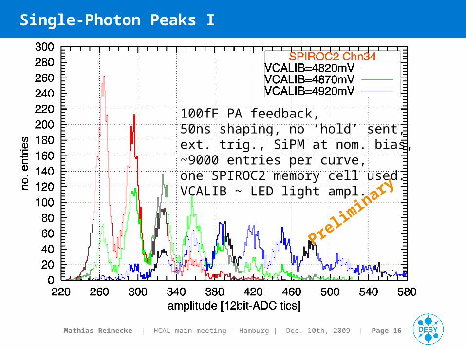
Single-Photon Peaks I
100fF PA feedback,50ns shaping, no ‘hold’ sent,ext. trig., SiPM at nom. bias,~9000 entries per curve,one SPIROC2 memory cell used.VCALIB ~ LED light ampl.
Prelim
inary
28 mar 2010 CdLT : ASIC developments in CALICE/EUDET LCWS 2010 17
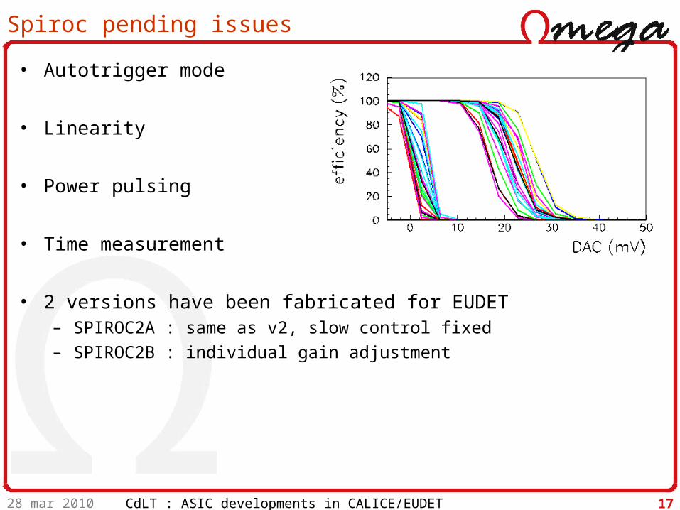
Spiroc pending issues
• Autotrigger mode
• Linearity
• Power pulsing
• Time measurement
• 2 versions have been fabricated for EUDET– SPIROC2A : same as v2, slow control fixed– SPIROC2B : individual gain adjustment
28 mar 2010 CdLT : ASIC developments in CALICE/EUDET LCWS 2010 18
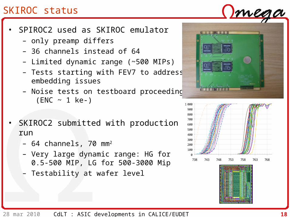
SKIROC status
• SPIROC2 used as SKIROC emulator– only preamp differs– 36 channels instead of 64– Limited dynamic range (~500 MIPs)– Tests starting with FEV7 to address
embedding issues– Noise tests on testboard proceeding
(ENC ~ 1 ke-)
• SKIROC2 submitted with production run– 64 channels, 70 mm2
– Very large dynamic range: HG for 0.5-500 MIP, LG for 500-3000 Mip
– Testability at wafer level 0
100
200
300
400
500
600
700
800
900
1 000
738 743 748 753 758 763 768
28 mar 2010 CdLT : ASIC developments in CALICE/EUDET LCWS 2010 19
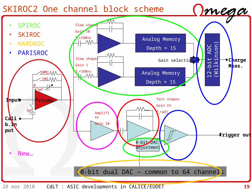
SKIROC2 One channel block scheme
1MΩ
0 3pF
Preamp.Input
10MΩ
3pF
Calib.Input
10-bit dual DAC – common to 64 channels
Analog Memory
Depth = 15
Analog Memory
Depth = 15
12-b
it A
DC
(Wilk
inso
n)
Trigger out
ChargeMeas.
Gain selection
Slow shaper
Gain 10
Tp=180ns
Slow shaper
Gain 1
Tp=180ns
Amplifier
Gain 10
fast shaper
Gain XX
Tp=adj
4-bit DACadjustment
• SPIROC• SKIROC• HARDROC• PARISROC
• New…
28 mar 2010 CdLT : ASIC developments in CALICE/EUDET LCWS 2010 20
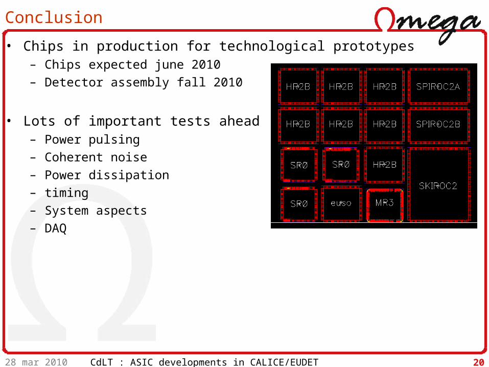
Conclusion
• Chips in production for technological prototypes– Chips expected june 2010– Detector assembly fall 2010
• Lots of important tests ahead– Power pulsing– Coherent noise– Power dissipation– timing– System aspects– DAQ
28 mar 2010 CdLT : ASIC developments in CALICE/EUDET LCWS 2010 21
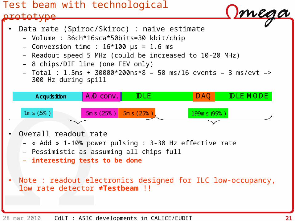
• Data rate (Spiroc/Skiroc) : naive estimate– Volume : 36ch*16sca*50bits=30 kbit/chip– Conversion time : 16*100 µs = 1.6 ms– Readout speed 5 MHz (could be increased to 10-20 MHz)– 8 chips/DIF line (one FEV only)– Total : 1.5ms + 30000*200ns*8 = 50 ms/16 events = 3 ms/evt => 300 Hz
during spill
• Overall readout rate– « Add » 1-10% power pulsing : 3-30 Hz effective rate– Pessimistic as assuming all chips full– interesting tests to be done
• Note : readout electronics designed for ILC low-occupancy, low rate detector ≠Testbeam !!
Test beam with technological prototype
Acquisition A/D conv. DAQ IDLE MODEChip 0
Chip 1 Acquisition A/D conv. DAQ IDLE MODEIDLE
Chip 2 Acquisition A/D conv. IDLE MODEIDLE
Chip 3 Acquisition A/D conv. IDLE MODEIDLE
Chip 4 Acquisition A/D conv. IDLE MODEIDLE DAQ
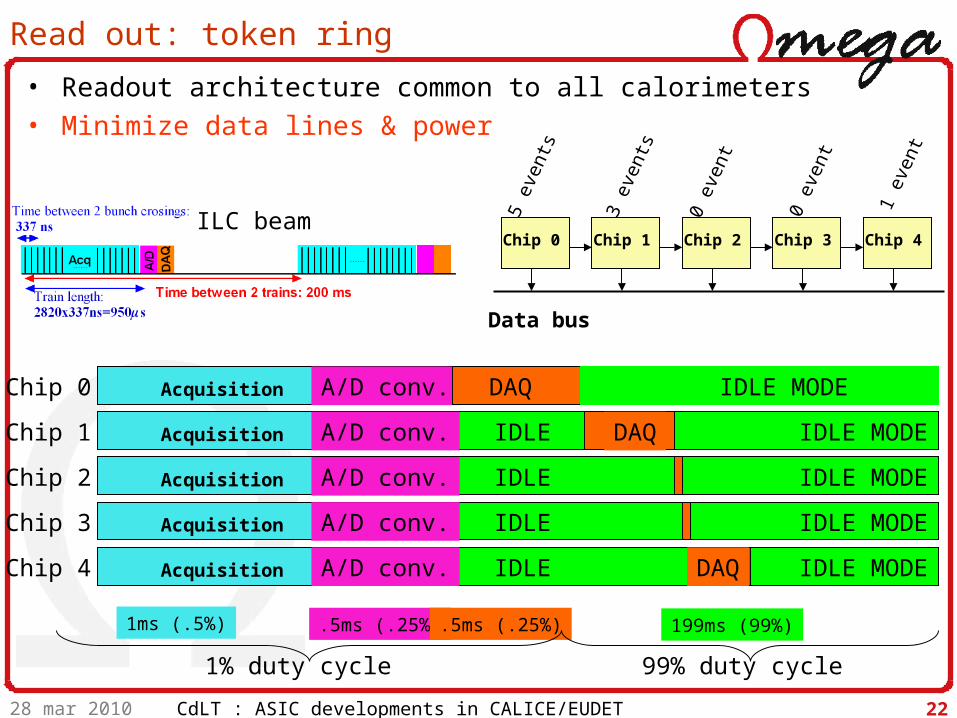
1ms (.5%) .5ms (.25%) .5ms (.25%) 199ms (99%)
Acquisition A/D conv. DAQ IDLE MODEChip 0
Chip 1 Acquisition A/D conv. DAQ IDLE MODEIDLE
Chip 2 Acquisition A/D conv. IDLE MODEIDLE
Chip 3 Acquisition A/D conv. IDLE MODEIDLE
Chip 4 Acquisition A/D conv. IDLE MODEIDLE DAQ
1ms (.5%) .5ms (.25%) .5ms (.25%) 199ms (99%)
28 mar 2010 CdLT : ASIC developments in CALICE/EUDET LCWS 2010 22
Read out: token ring
1% duty cycle 99% duty cycle
Acquisition A/D conv. DAQ IDLE MODEChip 0
Chip 1 Acquisition A/D conv. DAQ IDLE MODEIDLE
Chip 2 Acquisition A/D conv. IDLE MODEIDLE
Chip 3 Acquisition A/D conv. IDLE MODEIDLE
Chip 4 Acquisition A/D conv. IDLE MODEIDLE DAQ
1ms (.5%) .5ms (.25%) .5ms (.25%) 199ms (99%)
• Readout architecture common to all calorimeters• Minimize data lines & power
5 ev
ents
3 ev
ents
0 ev
ent
1 ev
ent
0 ev
ent
Chip 0 Chip 1 Chip 2 Chip 3 Chip 4
Data bus
ILC beam