Embed Size (px)
Citation preview
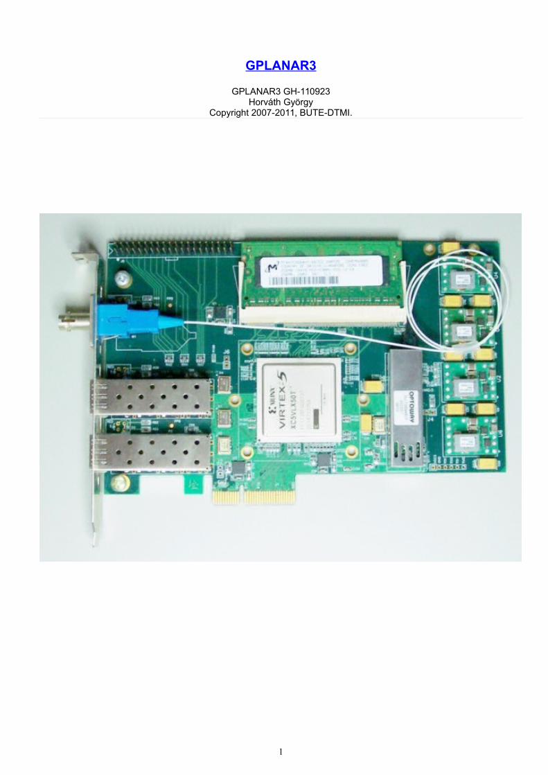
GPLANAR3
GPLANAR3 GH-110923Horváth György
Copyright 2007-2011, BUTE-DTMI.
1
Contents
GPLANAR3..........................................................................................................................................................................................1Contents.................................................................................................................................................................................................21. Introduction.......................................................................................................................................................................................3
1.1 What is GPLANAR3?.................................................................................................................................................................31.2 What is on-board?........................................................................................................................................................................31.3 Conformity...................................................................................................................................................................................4
2. Architecture.......................................................................................................................................................................................62.1 Power Supply...............................................................................................................................................................................72.2 Clock sources...............................................................................................................................................................................82.3 MultiRate/Standard Dual SFPs....................................................................................................................................................92.4 PCI Express x4 endpoint...........................................................................................................................................................102.5 GPON ONT Transceiver............................................................................................................................................................112.6 DDR2 SODIMM RAM.............................................................................................................................................................122.7 Feature Connector......................................................................................................................................................................142.8 FPGA Programming..................................................................................................................................................................16
2.8.1 Programming through JTAG..............................................................................................................................................162.8.2 Programming from FLASH................................................................................................................................................162.8.3 Partial reconfiguration........................................................................................................................................................172.8.4 Built-in JTAG programmer.................................................................................................................................................17
2.9 Status LEDs...............................................................................................................................................................................184. FPGA test Cores..............................................................................................................................................................................19
4.1 PCIEX4 - Endpoint Block for PCI Express v. 1.6.....................................................................................................................194.2 TEMAC - Virtex5 Embedded Tri-mode Ethernet MAC wrapper v. 1.3....................................................................................194.3 DDR2 - MIG v. 2.0 generated SODIMM teszt core..................................................................................................................204.4 STM16TRX - RocketIO GTP wizard v. 1.7..............................................................................................................................204.5 Clock domains...........................................................................................................................................................................20
2
1. Introduction
1.1 What is GPLANAR3?GPLANAR3 is a PCI-Express x4 adapter card, primarily developed for emulating GPON ONTs. It's on-board resources, and reconfigurability of its FPGA extends its functionality beyond the ONT emulation.
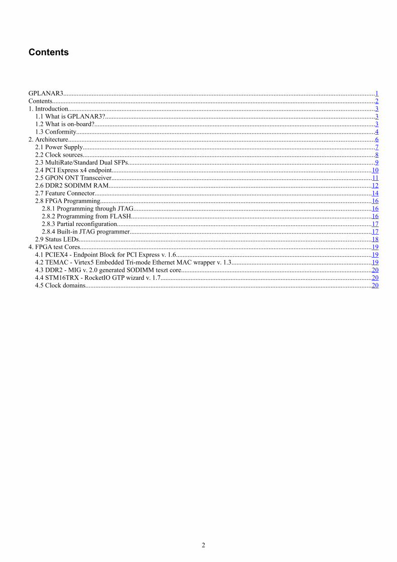
1.2 What is on-board?The figures below show the major on-board components.
Top side components:
1: GPON ONT Optical Subassembly (OSA)
2: Dual Gigabit Multi-Rate Multi-Standard SFP receptacle
3: DDR2 RAM SODIMM Receptacle 1.8V (Notebook RAM)
4: PCI Express x4 Edge Connector
5: 40 pin Berg type Feature Connector
6: Xilinx Virtex-5 family FPGA device
7: Switching regulators for 1.0, 1.8, 2.5, 3.3 Volts
9: JTAG connector for programming the FPGA or Flash
3
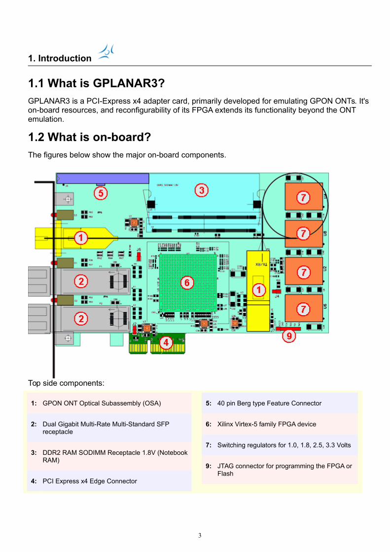
Bottom and ISA assembly side components:
8: Platform FLASH with initial FPGA core 10: Interface status LED's, RED/GREEN pairs
1.3 ConformityGPLANAR3 aims the following Standards/Recommendations:
GPON ITU-T G.984 series Gigabit Capable Passive Optical Network
ITU-T G.984.1 General characteristics
ITU-T G.984.2 Physical Media Dependent (PMD) layer specification
ITU-T G.984.3 Transmission convergence layer specification
SFP Small Formfactor Pluggable Transceivers
SFF Committee INF-8074i Specification for SFP Transceiver
SFF Committee SFF-8075 Specification for PCI Card Version of SFP Cage
SFF Committee SFF-8472 Specification for Diagnostic Monitoring Interface for Optical Xcvrs
...SDH Synchronous Digital Hierarchy
ITU-T G.707/Y.1322 Network node interface for the synchronous digital hierarchy (SDH)
4
...GBE Gigabit Ethernet (Optical/Copper)
IEEE Std 802.3 Carrier sense multiple access with collision detection (CSMA/CD) access method and physical layer specifications
PCIE PCI Express
PCI-SIG PCI Express Base Specification Revision 1.0a
PCI-SIG PCI Express Card Electromechanical Specification Revision 1.0a
DDR2 Dual DataRate II. SDRAM and Modules
JEDEC JESD79-2D DDR2 SDRAM SPECIFICATION
JEDEC No.21C 4.20.11 200-Pin DDR2 SDRAM Unbuffered SODIMM Design Specification. (Item #2017.10) Release No. 17
FC 40 pin Feature Connector
...PDH ITU-T G.703 Physical/electrical characteristics of hierarchical digital interfaces(.9 with passive feature card)
...HDD NCITS 361-2002 AT Attachment with Packet Interface - 6(ATA/ATAPI-6/UDMA5/UDMA100/UATA100 interface)
5
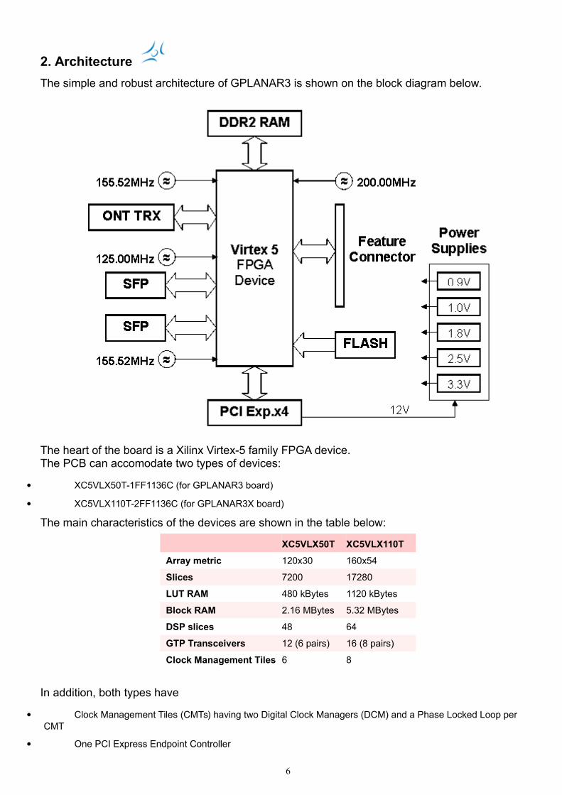
2. Architecture
The simple and robust architecture of GPLANAR3 is shown on the block diagram below.
The heart of the board is a Xilinx Virtex-5 family FPGA device.The PCB can accomodate two types of devices:
XC5VLX50T-1FF1136C (for GPLANAR3 board)
XC5VLX110T-2FF1136C (for GPLANAR3X board)
The main characteristics of the devices are shown in the table below:
XC5VLX50T XC5VLX110T
Array metric 120x30 160x54
Slices 7200 17280
LUT RAM 480 kBytes 1120 kBytes
Block RAM 2.16 MBytes 5.32 MBytes
DSP slices 48 64
GTP Transceivers 12 (6 pairs) 16 (8 pairs)
Clock Management Tiles 6 8
In addition, both types have
Clock Management Tiles (CMTs) having two Digital Clock Managers (DCM) and a Phase Locked Loop per CMT
One PCI Express Endpoint Controller
6
4 Tri-mode (10/100/1000)Ethernet Media Access Controller (MAC)
2 Internal Configuration Acces Ports (ICAP)
Core logic can run at 550MHz internal clock speed
Four GPLANAR3 models can be produced depending on the insertion of FPGA type, and the OLT transceiver as shown below:
Model FPGA ONT TRX
GPLANAR3 XC5VLX50T Yes
GPLANAR3S XC5VLX50T No
GPLANAR3X XC5VLX110T Yes
GPLANAR3SX XC5VLX110T No
The following sections detail the rest of the board's architectual elements.
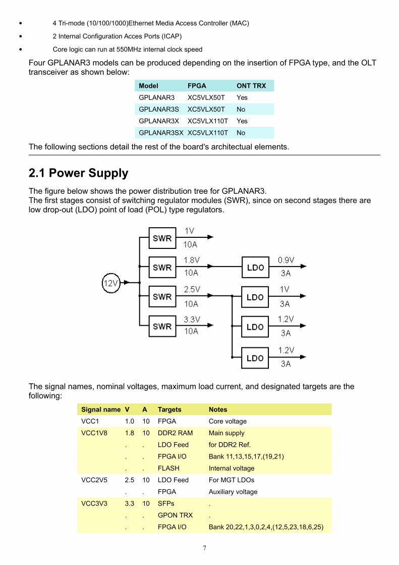
2.1 Power SupplyThe figure below shows the power distribution tree for GPLANAR3.The first stages consist of switching regulator modules (SWR), since on second stages there are low drop-out (LDO) point of load (POL) type regulators.
The signal names, nominal voltages, maximum load current, and designated targets are the following:
Signal name V A Targets Notes
VCC1 1.0 10 FPGA Core voltage
VCC1V8 1.8 10 DDR2 RAM Main supply
. . LDO Feed for DDR2 Ref.
. . FPGA I/O Bank 11,13,15,17,(19,21)
. . FLASH Internal voltage
VCC2V5 2.5 10 LDO Feed For MGT LDOs
. . FPGA Auxiliary voltage
VCC3V3 3.3 10 SFPs .
. . GPON TRX .
. . FPGA I/O Bank 20,22,1,3,0,2,4,(12,5,23,18,6,25)
7
. . Feature Conn. for I/O std. only
. . FLASH/JTAG I/O voltage
. . DDR2 Supply SPD ROM
VCC0V9 0.9 3 DDR2 Reference voltage
AVCC1 1.0 3 FPGA MGT MGT's core voltage
AVCPLL1V2 1.2 3 FPGA MGT MGT's PLL supply
AVCTX1V2 1.2 3 FPGA MGT MGT's Tx/Rx Supply
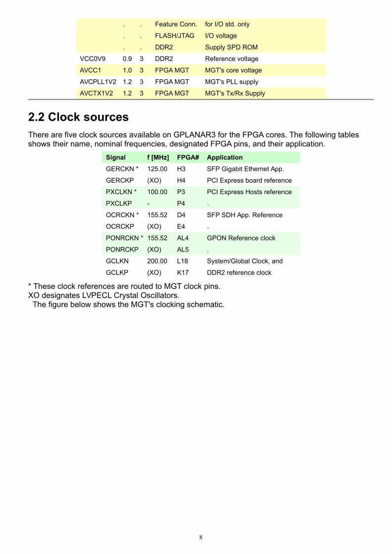
2.2 Clock sourcesThere are five clock sources available on GPLANAR3 for the FPGA cores. The following tables shows their name, nominal frequencies, designated FPGA pins, and their application.
Signal f [MHz] FPGA# Application
GERCKN * 125.00 H3 SFP Gigabit Ethernet App.
GERCKP (XO) H4 PCI Express board reference
PXCLKN * 100.00 P3 PCI Express Hosts reference
PXCLKP - P4 .
OCRCKN * 155.52 D4 SFP SDH App. Reference
OCRCKP (XO) E4 .
PONRCKN * 155.52 AL4 GPON Reference clock
PONRCKP (XO) AL5 .
GCLKN 200.00 L18 System/Global Clock, and
GCLKP (XO) K17 DDR2 reference clock
* These clock references are routed to MGT clock pins.XO designates LVPECL Crystal Oscillators. The figure below shows the MGT's clocking schematic.
8
2.3 MultiRate/Standard Dual SFPsThe GPLANAR3 board has two SFP module cages (P1,P2) that support user-installed SFP modules to support STM-1 to STM-16 (Synchronous Digital Hierarchy - SDH) and Gigabit Ethernetinterfaces.
Dedicated reference clock sources are available for both standards. 125MHz for GE, and 155.52MHz for SDH.
The GPLANAR3 board provides filtered 3.3V power to both SFP modules as per the SFP specification.
Since the receptacles are routed to one MGT pair, it is mandatory to install SFP's from homogenouos technology (rates may be different). It can not mix SDH and GE appclications.
The table below lists the connectors pins and any associated FPGA connectivity. Status LED's are also listed here.
Signal (P1) SFP# FPGA# Signal (P2) SFP# FPGA#
TXFAULT[0] 002 E13 TXFAULT[1] 002 D11
TXDIS[0] 003 G12 TXDIS[1] 003 E11
SDO[0] 004 E12 SDO[1] 004 D10
SCLK[0] 005 D12 SCLK[1] 005 E9
PLUG_N[0] 006 C13 PLUG_N[1] 006 F9
RATS[0] 007 A13 RATS[1] 007 E8
9
LOS[0] 008 B13 LOS[1] 008 F8
LEDACT_N[0] - G11 LEDACT_N[1] - C12
LEDLOS_N[0] - F11 LEDLOS_N[1] - B12
TXP[0] 019 B4 * TXP[1] 019 E2
TXN[0] 018 B3 TXN[1] 018 D2
RXP[0] 013 A3 RXP[1] 013 D1 **
RXN[0] 012 A2 RXN[1] 012 C1
GND 001 - GND 001 -
GND 009 - GND 009 -
GND 010 - GND 010 -
GND 011 - GND 011 -
GND 014 - GND 014 -
GND 017 - GND 017 -
GND 020 - GND 020 -
VCC3V3 015 - VCC3V3 015 -
VCC3V3 016 - VCC3V3 016 -
* TXPOLARITY attribute for the MGT has to be changed** RXPOLARITY attribute for the MGT has to be changed
2.4 PCI Express x4 endpointThe PCI Express endpoint connector (designated as J1 on-board) allows an FPGA design to support x1 and x4 gigabit lanes to communicate with the host, at the speed of 2.5 Gbps of each.
Caution! There is a jumper ( designated as J2 ) on board to select the proper presence detect lane configuration (close to x4) for the actual design.
The table below lists the connectors pins and any associated FPGA connectivity.
Signal (P1) Side A FPGA# Signal (P2) Side B FPGA#
PRESENT_N A1 - +12 VOLTS B1 To PWR
+12 VOLTS A2 To PWR +12 VOLTS B2 To PWR
+12 VOLTS A3 To PWR +12 VOLTS B3 To PWR
GND A4 - GND B4 -
JTAG_TCK A5 - SMCLK B5 -
JTAG_TDI A6 - SMDAT B6 -
JTAG_TDO A7 - GND B7 -
JTAG_TMS A8 - +3.3 VOLTS B8 -
+3.3 VOLTS A9 - JTAG_TRST_N B9 -
+3.3 VOLTS A10 - +3.3 VAUX B10 -
PXPERST A11 - PCIE_WAKE_N B11 -
KEY KEY KEY KEY KEY KEY
GND A12 - RESERVED B12 -
PXCLKP A13 P4 GND B13 -
PXCLKN A14 P3 PETP0 B14 N1
GND A15 - PETN0 B15 P1
PERP0 A16 M2 GND B16 -
10
PERN0 A17 N2 PRESENT_N B17 -
GND A18 - GND B18 -
RESERVED A19 - PETP1 B19 R1
GND A20 - PETN1 B20 T1
PERP1 A21 T2 GND B21 -
PERN1 A22 U2 GND B22 -
GND A23 - PETP2 B23 W1
GND A24 - PETN2 B24 Y1
PERP2 A25 V2 GND B25 -
PERN2 A26 W2 GND B26 -
GND A27 - PETP3 B27 AA1 **
GND A28 - PETN3 B28 AB1
PERP3 A29 AB2 * GND B29 -
PERN3 A30 AC2 --- B30 -
GND A31 - PRESENT4_N B31 To J2
--- --- - GND B32 -
* RXPOLARITY attribute for the MGT has to be changed** TXPOLARITY attribute for the MGT has to be changed
Although the PCI identification codes are FPGA core dependeant, defaults are the following:
Vendor ID........ 15C6 ..... Technical University of Budapest Device ID........ 02E3 ..... GPLANA 2.4 Gbps GPON ONU Emulator Revision ID...... 1 ..... Rev. 1. (GPLANAR3) Base Class....... 02 ..... Network controller Sub-Class........ 80 ..... Other network controller Interface........ 0 ..... Base model, XC5VLX50T+ONT Interface........ 1 ..... Extra (X), XC5VLX110T+ONT Interface........ 2 ..... Limited (S), XC5VLX50T, no ONT Interface........ 3 ..... Limited Extra(SX), XC5VLX110T, no ONT
2.5 GPON ONT TransceiverGPLANAR3 aims the emulation of multiple GPON ONUs. (Optical Network Unit). The main part of the ONU is the ONT (Optical Network Termination) transceiver - designated as P3.
ONT functions are entirelly implemented in the FPGA core. The rest of ONUs may be constructed using on-board, or host's resources. Here are some examples below:
Two pieces of real ATM (Asynchronous Transfer Mode) interface can be implemented by plugging 155Mbps SFP transceivers into P1 and P2, with the corresponding FPGA core support
Four real PDH interfaces can be attached to the Feature Connector (passive card required - see FC section) for ISDN PRI applications.
Good number of 10/100Mbps Ethernet interfaces can be intruduced to the host computer, running several virtual machines (e.g. VmWare). The limit is the 8Gbps full duplex bandwidth of the PCI Ecpress x4 interface.
Virtual endpoints of any kind can be constructed in the FPGA fabric, using the 256Mbytes RAM module to store their states and properties.
The table below summarizes the transceiver signals for ONT, and the corresponding FPGA pin numbers.
Signal Function FPGA#
RD3P * Receive downstream AP2
11
RD3N (2.48832 Gbps) AP3
TD3P ** Burst Transmission AN3
TD3N (1.24416 Gbps) AN4
SD3 RX Signal Detect AP14
BEN3 TX Burst Enable AN14
* RXPOLARITY attribute for the MGT has to be changed** TXPOLARITY attribute for the MGT has to be changed
2.6 DDR2 SODIMM RAMThe GPLANAR3 board contains a 200-pin, small-outline dual in-line memory module (SODIMM) receptacle ( J3 ) that supports installation of DDR2 SDRAM SODIMMs of 128MB, 256MB, or 512 MB.
Dual-rank SODIMMs may not be supported. Also, the speed grade of -1 of the default FPGA installation limits the DDR2 memory clock support to a range of 200-233MHz (400-466 million transfers per second - double rate).
A 256MB DDR2-667 SODIMM (Micron Semiconductor part number MT4HTF3264HY-667D3) is shipped with GPLANAR3 - by default.
The SODIMM interface may support customer installation of DDR2-533 and/or DDR2-400 SODIMMs too.
The table below provides a description of the memory interface signals SODIMM connector pin assignments, and the associated FPGA pin assignments.
Signal (Front) DIMM# FPGA# Signal (Back) DIMM# FPGA#
VCC0V9 001 - GND 002 -
GND 003 - DQ[4] 004 H29
DQ[0] 005 L29 DQ[5] 006 G30
DQ[1] 007 J29 GND 008 -
GND 009 - DM[0] 010 H30
DQS_N[0] 011 F29 GND 012 -
DQS[0] 013 E29 DQ[6] 014 F30
GND 015 - DQ[7] 016 G31
DQ[2] 017 P29 GND 018 -
DQ[3] 019 P30 DQ[12] 020 L30
GND 021 - DQ[13] 022 K31
DQ[8] 023 F31 GND 024 -
DQ[9] 025 E31 DM[1] 026 J31
GND 027 - GND 028 -
DQS_N[1] 029 N30 CK[0] 030 B32
DQS[1] 031 M31 CK_N[0] 032 A33
GND 033 - GND 034 -
DQ[10] 035 P31 DQ[14] 036 M30
DQ[11] 037 R31 DQ[15] 038 N29
GND 039 - GND 040 -
GND 041 - GND 042 -
12
DQ[16] 043 B33 DQ[20] 044 C34
DQ[17] 045 C33 DQ[21] 046 D34
GND 047 - GND 048 -
DQS_N[2] 049 E34 NC/EVENT_N 050 -
DQS[2] 051 F33 DM[2] 052 E33
GND 053 - GND 054 -
DQ[18] 055 F34 DQ[22] 056 C32
DQ[19] 057 E32 DQ[23] 058 D32
GND 059 - GND 060 -
DQ[24] 061 H34 DQ[28] 062 G33
DQ[25] 063 H33 DQ[29] 064 G32
GND 065 - GND 066 -
DM[3] 067 J34 DQS_N[3] 068 K34
NC/RESET_N 069 - DQS[3] 070 L34
GND 071 - GND 072 -
DQ[26] 073 K32 DQ[30] 074 J32
DQ[27] 075 L33 DQ[31] 076 K33
GND 077 - GND 078 -
CKE[0] 079 N32 CKE[1] 080 M32
VCC1V8 081 - VCC1V8 082 -
NC/CSN[2] 083 - A[15] 084 R32
BA[2] 085 P32 A[14] 086 R33
VCC1V8 087 - VCC1V8 088 -
A[12] 089 U31 A[11] 090 T33
A[9] 091 P34 A[7] 092 U32
A[8] 093 V25 A[6] 094 U33
VCC1V8 095 - VCC1V8 096 -
A[5] 097 W29 A[4] 098 Y28
A[3] 099 R34 A[2] 100 V29
A[1] 101 V24 A[0] 102 AA30
VCC1V8 103 - VCC1V8 104 -
A[10] 105 W26 BA[1] 106 W31
BA[0] 107 V27 RAS_N 108 AA31
WE_N 109 V28 CS_N[0] 110 Y31
VCC1V8 111 - VCC1V8 112 -
CAS_N 113 Y29 ODT[0] 114 T34
CS_N[1] 115 AA29 A[13] 116 AB31
VCC1V8 117 - VCC1V8 118 -
ODT[1] 119 V30 NC/CSN[3] 120 -
GND 121 - GND 122 -
DQ[32] 123 V32 DQ[36] 124 Y33
DQ[33] 125 V33 DQ[37] 126 Y32
GND 127 - GND 128 -
DQS_N[4] 129 V34 DM[4] 130 AB32
13
DQS[4] 131 W34 GND 132 -
GND 133 - DQ[38] 134 Y34
DQ[34] 135 AA33 DQ[39] 136 AA34
DQ[35] 137 AB33 GND 138 -
GND 139 - DQ[44] 140 AD32
DQ[40] 141 AC32 DQ[45] 142 AK32
DQ[41] 143 AC33 GND 144 -
GND 145 - DQS_N[5] 146 AD34
DM[5] 147 AE33 DQS[5] 148 AC34
GND 149 - GND 150 -
DQ[42] 151 AE32 DQ[46] 152 AF33
DQ[43] 153 AE34 DQ[47] 154 AF34
GND 155 - GND 156 -
DQ[48] 157 AH34 DQ[52] 158 AM33
DQ[49] 159 AJ34 DQ[53] 160 AK34
GND 161 - GND 162 -
NC/TEST 163 - CK[1] 164 AN34
GND 165 - CK_N[1] 166 AN33
DQS_N[6] 167 AL33 GND 168 -
DQS[6] 169 AL34 DM[6] 170 AN32
GND 171 - GND 172 -
DQ[50] 173 AK33 DQ[54] 174 AP32
DQ[51] 175 AJ32 DQ[55] 176 AM32
GND 177 - GND 178 -
DQ[56] 179 AF31 DQ[60] 180 AK31
DQ[57] 181 AG30 DQ[61] 182 AD30
GND 183 - GND 184 -
DM[7] 185 AF30 DQS_N[7] 186 AH30
GND 187 - DQS[7] 188 AJ30
DQ[58] 189 AD29 GND 190 -
DQ[59] 191 AE29 DQ[62] 192 AH29
GND 193 - DQ[63] 194 AF29
SDA 195 AH19 GND 196 -
SCL 197 AF19 SA0 198 (GND)
VCC3V3 199 - SA1 200 (GND)
2.7 Feature ConnectorMainly for historical reason, a 40 pins BERG type Feature Connector ( designated as J5 ) is used for GPLANAR3.
The table below shows the pinout assignment for FPGA cores implementing IDE/HDD applications.
Signal (even) J5# FPGA# . Signal (odd) J5# FPGA#
FRST 01 H14 GND 02 -
14
FD[7] 03 J14 FD[8] 04 H20
FD[6] 05 K14 FD[9] 06 J20
FD[5] 07 L14 FD[10] 08 L20
FD[4] 09 G15 FD[11] 10 J21
FD[3] 11 H15 FD[12] 12 K21
FD[2] 13 J15 FD[13] 14 L21
FD[1] 15 L15 FD[14] 16 G22
FD[0] 17 G16 FD[15] 18 H22
GND 19 - FKEY 20 J22
FDRQ 21 J16 GND 22 -
FIOWN 23 K16 GND 24 -
FIORN 25 L16 GND 26 -
FIORDY 27 H17 FBALE 28 K22
FDACKN 29 J17 GND 30 -
FIRQ 31 H18 FIOCSN 32 G23
FA[1] 33 K18 GND 34 -
FA[0] 35 H19 FA[2] 36 H23
FCSN[0] 37 J19 FCSN[1] 38 L19
FACT 39 K19 GND 40 -
For PDH applications, a passive child board (type D1558001-LIU) has to be connected to J5. The pinout can be found in the table below.
Signal (even) J5# FPGA# . Signal (odd) J5# FPGA#
NC 01 H14 GND 02 -
TTXA[0] 03 J14 TTXB[0] 04 H20
RTXA[0] 05 K14 TTXB[0] 06 J20
TTXA[1] 07 L14 TTXA[1] 08 L20
RTXA[1] 09 G15 RTXA[1] 10 J21
TTXA[2] 11 H15 TTXA[2] 12 K21
RTXA[2] 13 J15 RTXA[2] 14 L21
TTXA[3] 15 L15 TTXA[3] 16 G22
RTXA[3] 17 G16 RTXA[3] 18 H22
GND 19 - NC 20 J22
TRX[0] 21 J16 GND 22 -
NC 23 K16 GND 24 -
RRX[0] 25 L16 GND 26 -
NC 27 H17 NC 28 K22
RRX[1] 29 J17 GND 30 -
TRX[1] 31 H18 NC 32 G23
TRX[2] 33 K18 GND 34 -
RRX[2] 35 H19 NC 36 H23
TRX[3] 37 J19 NC 38 L19
RRX[3] 39 K19 GND 40 -
15
TTX signals drives the TIP side pulses, RTX signals drives RING.RRX and TRX signals carry received pulses (RING and TIP).
Note that TTXA and TTXB signals are bound together on the child board to achive the 3 volts peakvoltage of the transmitted pulses. (conforming ITU-T Rec. G.703) Crosscurrent glitches are limited by serial resistors on GPLANAR3 card.
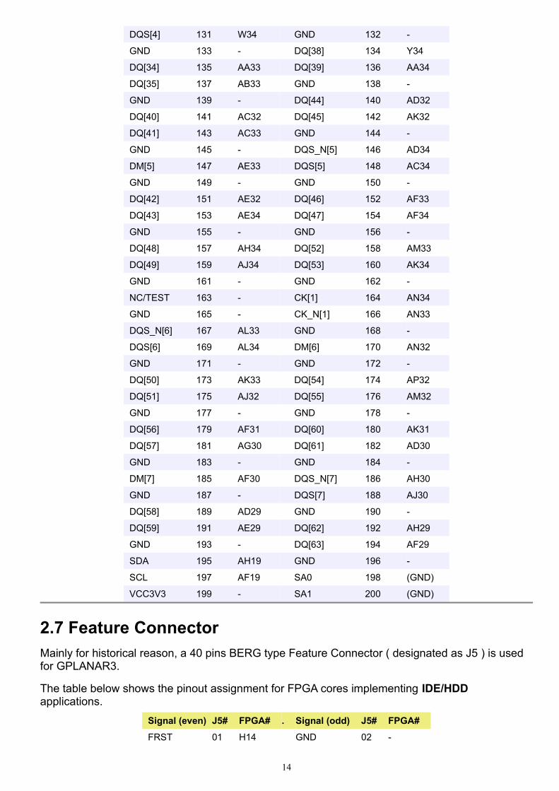
The child board has four interfaces with RJ12 connectors, as shown below.
2.8 FPGA ProgrammingThree configuration methods are available on GPLANAR3 to upload (program) the FPGA core.
2.8.1 Programming through JTAG
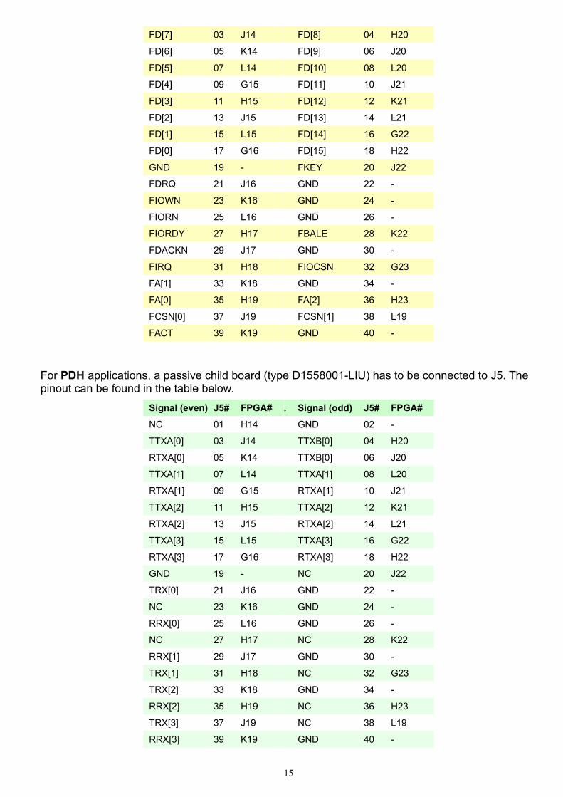
FPGA core can be loaded directly through the JTAG port (designated as J7 on-board) as shown in the figure below
2.8.2 Programming from FLASH
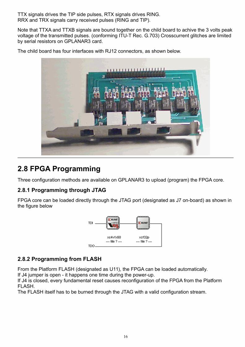
From the Platform FLASH (designated as U11), the FPGA can be loaded automatically.If J4 jumper is open - it happens one time during the power-up.If J4 is closed, every fundamental reset causes reconfiguration of the FPGA from the Platform FLASH.The FLASH itself has to be burned through the JTAG with a valid configuration stream.
16
2.8.3 Partial reconfiguration
If the Platform FLASH contains the proper core implementing a PCI Express endpoint, and a controller core for ICAP (Internal Configuration Access Port) - this RESIDENT core allows the Partial reconfiguration of the FPGA.TRANSIENT cores can be loaded that way.
J6 jumper controls HSWAPEN.
2.8.4 Built-in JTAG programmer
An internal JTAG programmer can be implemented in the FPGA. The pinout for the internal programmer:
J11# Signal FPGA#1 ITCK AG152 ITDO AG163 ITDI AH174 ITMS AG17
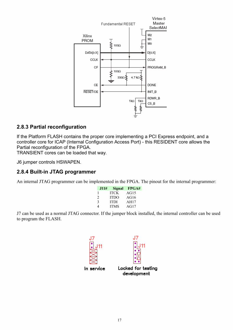
J7 can be used as a normal JTAG connector. If the jumper block installed, the internal controller can be used to program the FLASH.
17
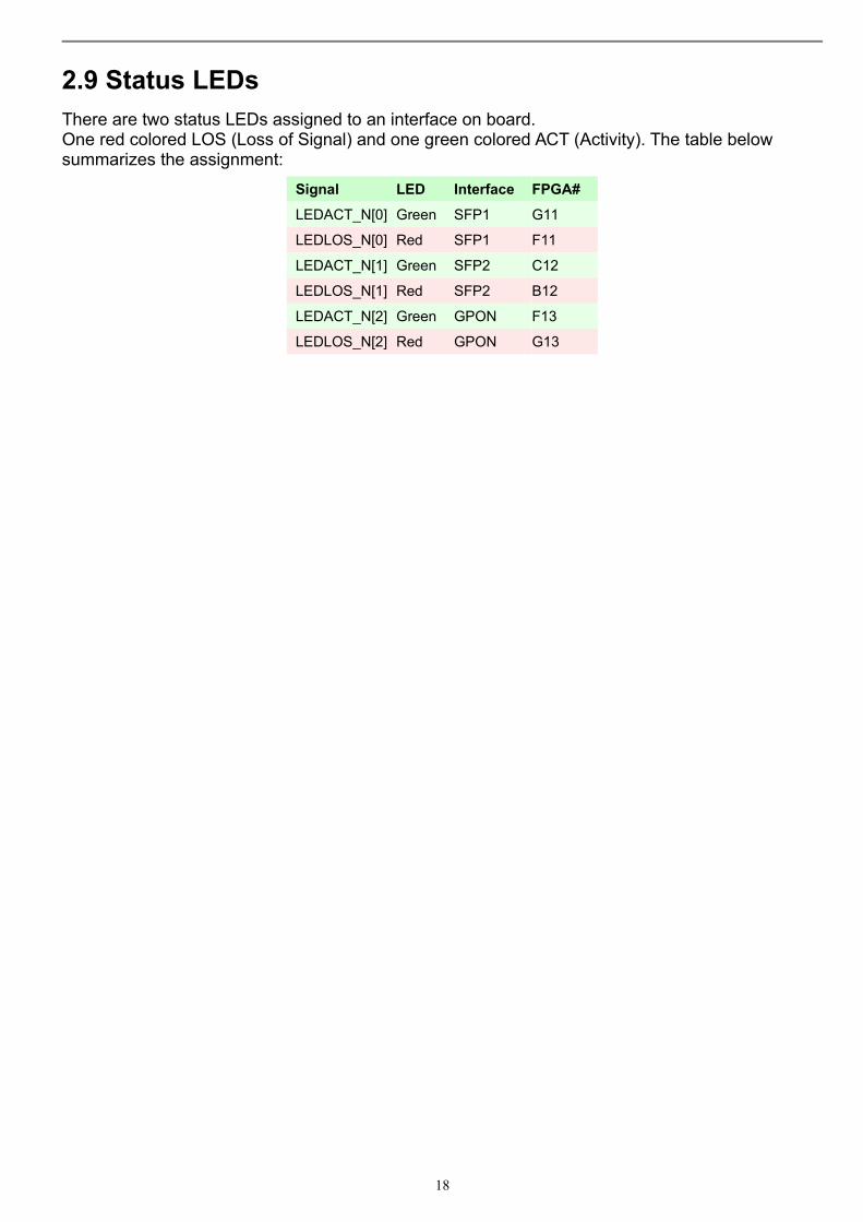
2.9 Status LEDsThere are two status LEDs assigned to an interface on board.One red colored LOS (Loss of Signal) and one green colored ACT (Activity). The table below summarizes the assignment:
Signal LED Interface FPGA#
LEDACT_N[0] Green SFP1 G11
LEDLOS_N[0] Red SFP1 F11
LEDACT_N[1] Green SFP2 C12
LEDLOS_N[1] Red SFP2 B12
LEDACT_N[2] Green GPON F13
LEDLOS_N[2] Red GPON G13
18
4. FPGA test Cores
The on-board subsystems have been successfully tested using the Xilinx's Coregen generated cores. User Constraints files were modified according to the boards metric. Further modifications are discussed below on a per-Core bases.
These test Cores are available in the Distribution media:
4.1 PCIEX4 - Endpoint Block for PCI Express v. 1.6This core implements a PCI Express x4 endpoint, with a completer allowing R/W access to the on-chip RAM block.
Little modifications were made to the orignal top level design. Red LED's above P1, P2, and P3 signal failures.P1 - PLLLKDET lit if the GTP's PLL is not locked.P2 - LINKUP lit if link training have failed for the lanes.P3 - CLKLOCK lit if the on-chip PLL_ADV did not locked.
In order to report the presence of all four lanes, J2 has to be closed. Closing J4 forces the FPGA tobe reloaded from the Platform Flash when the OS restarts, or the reset button is pushed on the PC.
Using the Microsoft Windows XP operating system, GPLANAR3 is found as a new hardware with the following ID's:
Vendor: 15C6 - BUTEDevice: 02E3 - 2.4 Gbps GPON ONU EmulatorRevision: 1Base Class: 02 - NetworkSubclass: 80 - Other
4.2 TEMAC - Virtex5 Embedded Tri-mode Ethernet MAC wrapper v. 1.3
The dual-SFP subystems have been successfully tested using the Xilinx's TEMAC core. The example design Autonegotiates with the other party, and send back every ethernet frames with the SRC and DST addresses swapped.
Our test suite consists of a Cisco Catalyst 3500 XL having a GBIC optical module type D-Link DGS-707, and a GPLANAR3 board having a SFP optical module type D-Link DEM-311GT.Both P1 and P2 receptacle were tested successfully.
Little modifications were made to the orignal top level design.In temac.vhd the EMAC0_PHYINIT_AUTONEG_ENABLE and EMAC1_PHYINIT_AUTONEG_ENABLE were set to TRUE. Also the GTP's TX/RX POLARITY were changed - reflecting the boards routing strategy. Red LED's above P1, P2, and P3 signal failures.P1 - EMAC0CLIENTSYNCACQSTATUS lit if failed to acquired the synchron.P2 - EMAC1CLIENTSYNCACQSTATUS lit if failed to acquired the synchron.
Green LED's above P1, P2, and P3 acts as described below.P1 - LOS lit if signal present. (no Losss Of Signal)P2 - LOS lit if signal present. (no Losss Of Signal)P3 - testcnb(26) Blinks slowly if 200 MHz global clock is OK. This signal is not related to the TEMAC core, it is just for testing.
19
The test is passed if the interface status LED of the switch is green (link is up), and GPLANAR3 shows green lit for all LEDs (P3 blinks slowly).
4.3 DDR2 - MIG v. 2.0 generated SODIMM teszt coreGPLANAR3 has a 256 MBytes DDR2-400 SODIMM type MT4HTF3264HY-667 installed by default. The Memory Interface Generator produced a test core that initialize the module, and performs continuous R/W tests.
Little modifications were made to the orignal top level design.Red LED's above P1 signals failure.P1 - phy_init_done lit if failed to initialize the module.
Green LED's above P1, P2 acts as described below.P1 - error lit if the R/W test does not reveal bit errors. This signal is latched. Close pin 1 and 20 onthe feature connector to reset the core in order to restart the test.P2 - testcnt(26) Blinks slowly if 200 MHz global clock is OK.
The test is passed if GPLANAR3 shows green lit for all LEDs (P2 blinks slowly).
4.4 STM16TRX - RocketIO GTP wizard v. 1.7Although the GPON SFF transceiver has no stand-alone test core (yet), STM16TRX core tests the involved GTP tile in serial PMA loopback mode.
The GTP wizard generated example design contains a SDH/SONET like frame generator, and a frame checker (payload inclusive).
Some modifications were made to the orignal top level design example_mgt_top.vhd, and to the frame checker frame_check.vhd.
The error counts from the transceivers were wired out to the feature connector. GTP0 errors to FD(0..7) since GTP1 to FD(8..15). Note that GTP0 in this tile is not connected, since GTP1 is connected to the GPON ONT transceiver,
Red LED's above P1, P2, and P3 functions:P1 - framesync0 lit if the frame checker 0 can not acquire the frame synchron.P2 - framesync1 lit if the frame checker 1 can not acquire the frame synchron.P3 - testcnt(26) blinks slowly if TX clock is OK.
Green LED's above P1, P2, and P3 acts as described below.P1 - errorlat0 lit if no bit error has occured yet during the frame checkP2 - errorlat1 lit if no bit error has occured yet during the frame checkP3 - testcnb(26) blinks slowly if RX recovered clock is OK.
The test is passed if GPLANAR3 shows green lit P1,P2, and P3 LEDs blink slowly.
4.5 Clock domainsThe following table summarizes the proposed clock domains to help devloping new/combined FPGA Cores.
It can also be used for estimating the performace of core by using the data bits column for a given clock rate.
Signal f [MHz] FPGA Res. Core D bits Source
core_clk 250.00 1 PLL_ADV pciex4 n.a. Slot clock (100MHz)
user_clk 125.00 see above pciex4 64 Slot clock (100MHz)
clk200 200.00 see below ddr2 n.a. Crystal Osc. X4
20
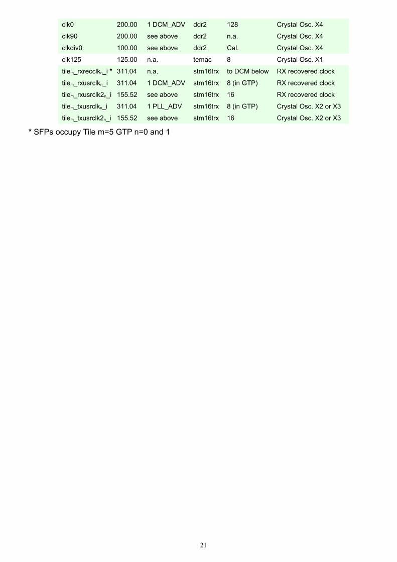
clk0 200.00 1 DCM_ADV ddr2 128 Crystal Osc. X4
clk90 200.00 see above ddr2 n.a. Crystal Osc. X4
clkdiv0 100.00 see above ddr2 Cal. Crystal Osc. X4
clk125 125.00 n.a. temac 8 Crystal Osc. X1
tilem_rxrecclkn_i * 311.04 n.a. stm16trx to DCM below RX recovered clock
tilem_rxusrclkn_i 311.04 1 DCM_ADV stm16trx 8 (in GTP) RX recovered clock
tilem_rxusrclk2n_i 155.52 see above stm16trx 16 RX recovered clock
tilem_txusrclkn_i 311.04 1 PLL_ADV stm16trx 8 (in GTP) Crystal Osc. X2 or X3
tilem_txusrclk2n_i 155.52 see above stm16trx 16 Crystal Osc. X2 or X3
* SFPs occupy Tile m=5 GTP n=0 and 1
21