Embed Size (px)
Citation preview

©2021 IEEE. Personal use of this material is permitted. Permission from IEEE must be obtained for allother uses, in any current or future media, including reprinting/republishing this material for advertisingor promotional purposes, creating new collective works, for resale or redistribution to servers or lists, orreuse of any copyrighted component of this work in other works.
This work has been submitted to the IEEE for possible publication. Copyright may be transferredwithout notice, after which this version may no longer be accessible.
This work was submitted to IEEE Signal Processing Society’s ASILOMAR Conference onSignals, Systems and Computers on the midnight of May 8, 2021.
If this paper is accepted by the conference, this pre-print will be replaced by the accepted versionof the paper with the DOI and an appropriate copyright notice from IEEE.

Compute RAMs: Adaptable Compute and StorageBlocks for DL-Optimized FPGAs
Aman Arora∗, Bagus Hanindhito†, Lizy K. John‡Department of Electrical and Computer Engineering
The University of Texas at Austin∗[email protected], †[email protected], ‡[email protected]
Abstract—The configurable building blocks of current FPGAs— Logic blocks (LBs), Digital Signal Processing (DSP) slices,and Block RAMs (BRAMs) — make them efficient hardwareaccelerators for the rapid-changing world of Deep Learning (DL).Communication between these blocks happens through an inter-connect fabric consisting of switching elements spread throughoutthe FPGA. In this paper, a new block, Compute RAM, isproposed. Compute RAMs provide highly-parallel processing-in-memory (PIM) by combining computation and storage capabili-ties in one block. Compute RAMs can be integrated in the FPGAfabric just like the existing FPGA blocks and provide two modesof operation (storage or compute) that can be dynamically chosen.They reduce power consumption by reducing data movement,provide adaptable precision support, and increase the effectiveon-chip memory bandwidth. Compute RAMs also help increasethe compute density of FPGAs. In our evaluation of addition,multiplication and dot-product operations across multiple dataprecisions (int4, int8 and bfloat16), we observe an average savingsof 80% in energy consumption, and an improvement in executiontime ranging from 20% to 80%. Adding Compute RAMs canbenefit non-DL applications as well, and make FPGAs moreefficient, flexible, and performant accelerators.
I. INTRODUCTION
Deep Learning (DL) has become ubiquitous in today’sworld. The ever-increasing computational demands of DL ap-plications has triggered an explosion of hardware accelerationalternatives, ranging from ASICs to GPUs to FPGAs. FPGAsare well-suited to the evolving needs of DL applicationsbecause they provide customizable hardware with massiveparallelism and energy efficiency.
FPGAs contain fine-grained programmable logic (e.g.,LBs), fixed-function math units (e.g., DSP slices), and embed-ded memory structures (e.g., BRAMs) that can be connectedby a configurable interconnection fabric. These building blocksare very generic, making FPGAs a great solution to designvarious accelerator, but this flexibility, unfortunately, limits theperformance we can achieve with FPGAs for DL applications.In recent years, DL-optimized FPGA architectures have beenproposed and deployed, such as adding vector processors[1] and integrating DL-specific blocks [2] [3] on the FPGAchip. Most FPGA vendors have added support for smaller,DL-friendly precisions (e.g., 8-bit fixed-point (int8) andbfloat16 [4]) in DSP slices.
Even so, there are still some limitations in current FPGAarchitectures. Separation of compute units (LBs and DSPs)from storage units (BRAMs) leads to a lot of data movement
to feed the compute units with input data and to store theoutputs back to the storage units. This is exacerbated for DLapplications because of the math-intensive nature of operationsinvolved in them. This data movement, although on-chip,is expensive in terms of power consumption because themovement happens through the FPGA interconnect whichcomprises of numerous switches instead of hard connectedwires. This flexible but inefficient interconnect also leads toslower frequencies for designs on FPGAs (typically 3-4x lowerthan ASICs [5]).
BRAMs on FPGAs support a limited set of heights andwidths. For example, BRAMs in Intel Stratix 10 [6] are 20Kilobits in size and can be configured as 512x40, 1024x20 and2048x10 bits, with only 1 or 2 read and write ports. Owing tothe parallel nature of DL applications, it is common to processthousands of bits of data together. It is preferred for users tosplit the data over multiple BRAMs for higher bandwidth, withonly a few rows of each block are utilized.
Another limitation is the limited number of precisionssupported by the DSP slices. For example, DSP slices in IntelAgilex FPGAs [7] support multiplication and MAC (multiply-accumulate) operations in 9x9, 27x27, 18x19 fixed-point and16-bit or 32-bit floating-point precisions. Although DSP sliceshave become more complex over the years to support moreprecisions, the precision requirements change rapidly, espe-cially in the world of DL. Users have to implement math unitson LBs instead, reducing the number of LBs available for otherpurposes and leaving DSPs unused.
In this paper, we propose adding a new type of block, calledCompute RAM, to FPGAs. A Compute RAM block enablescomputation within the RAM array, without transferringthe data in or out of it. The implementation of these blocks isbased on an emerging Logic-in-Memory SRAM prototype byJeloka et. al. [8]. Using this technology and its extensions (bit-line computing [9] and bit-serial arithmetic [10]), processing-in-memory engines can be designed. For Compute RAMs, weadd components to such SRAMs to integrate them into theFPGA fabric and make them configurable. Compute RAMscan be programmed during FPGA configuration time or duringrun-time. The user to perform math in any precision usingCompute RAMs. Every column of the memory performs thesame operation simultaneously, resulting in massive paral-lelism and high throughput. An operation can be performed percolumn in the Compute RAM, thereby dramatically reducing
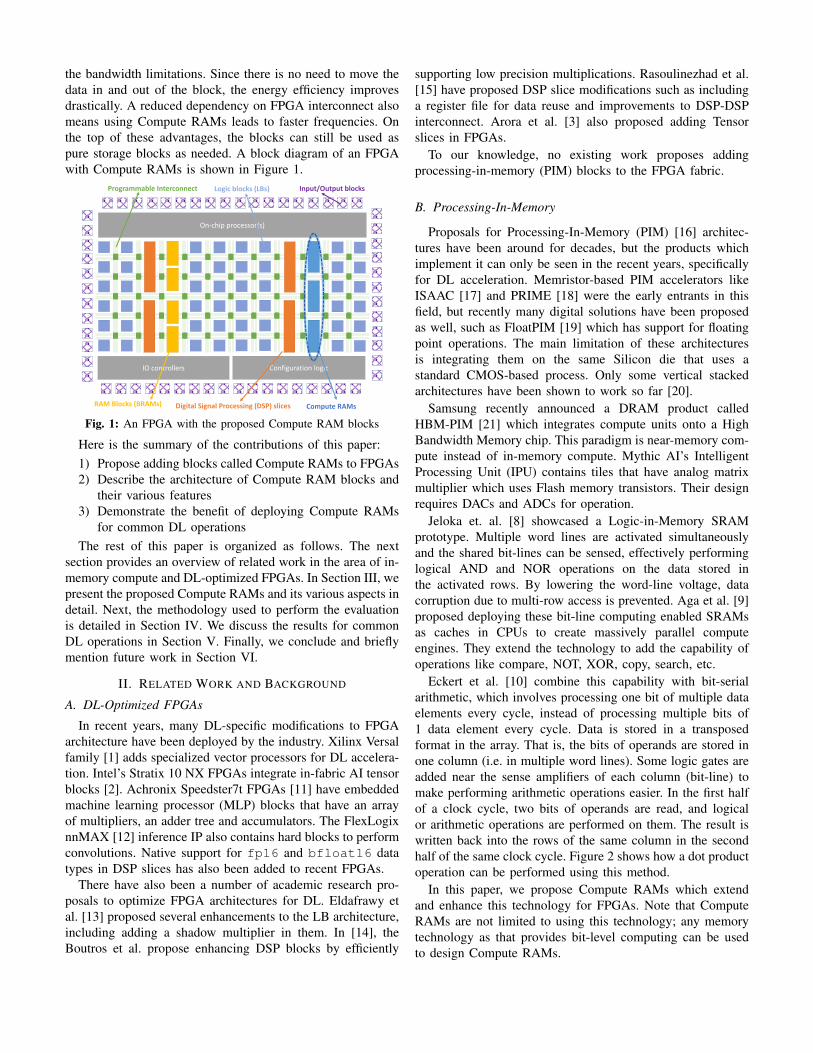
the bandwidth limitations. Since there is no need to move thedata in and out of the block, the energy efficiency improvesdrastically. A reduced dependency on FPGA interconnect alsomeans using Compute RAMs leads to faster frequencies. Onthe top of these advantages, the blocks can still be used aspure storage blocks as needed. A block diagram of an FPGAwith Compute RAMs is shown in Figure 1.
On-chip processor(s)
Configuration logicIO controllers
Programmable Interconnect Logic blocks (LBs) Input/Output blocks
Digital Signal Processing (DSP) slicesRAM Blocks (BRAMs) Compute RAMs
Fig. 1: An FPGA with the proposed Compute RAM blocks
Here is the summary of the contributions of this paper:1) Propose adding blocks called Compute RAMs to FPGAs2) Describe the architecture of Compute RAM blocks and
their various features3) Demonstrate the benefit of deploying Compute RAMs
for common DL operationsThe rest of this paper is organized as follows. The next
section provides an overview of related work in the area of in-memory compute and DL-optimized FPGAs. In Section III, wepresent the proposed Compute RAMs and its various aspects indetail. Next, the methodology used to perform the evaluationis detailed in Section IV. We discuss the results for commonDL operations in Section V. Finally, we conclude and brieflymention future work in Section VI.
II. RELATED WORK AND BACKGROUND
A. DL-Optimized FPGAs
In recent years, many DL-specific modifications to FPGAarchitecture have been deployed by the industry. Xilinx Versalfamily [1] adds specialized vector processors for DL accelera-tion. Intel’s Stratix 10 NX FPGAs integrate in-fabric AI tensorblocks [2]. Achronix Speedster7t FPGAs [11] have embeddedmachine learning processor (MLP) blocks that have an arrayof multipliers, an adder tree and accumulators. The FlexLogixnnMAX [12] inference IP also contains hard blocks to performconvolutions. Native support for fp16 and bfloat16 datatypes in DSP slices has also been added to recent FPGAs.
There have also been a number of academic research pro-posals to optimize FPGA architectures for DL. Eldafrawy etal. [13] proposed several enhancements to the LB architecture,including adding a shadow multiplier in them. In [14], theBoutros et al. propose enhancing DSP blocks by efficiently
supporting low precision multiplications. Rasoulinezhad et al.[15] have proposed DSP slice modifications such as includinga register file for data reuse and improvements to DSP-DSPinterconnect. Arora et al. [3] also proposed adding Tensorslices in FPGAs.
To our knowledge, no existing work proposes addingprocessing-in-memory (PIM) blocks to the FPGA fabric.
B. Processing-In-Memory
Proposals for Processing-In-Memory (PIM) [16] architec-tures have been around for decades, but the products whichimplement it can only be seen in the recent years, specificallyfor DL acceleration. Memristor-based PIM accelerators likeISAAC [17] and PRIME [18] were the early entrants in thisfield, but recently many digital solutions have been proposedas well, such as FloatPIM [19] which has support for floatingpoint operations. The main limitation of these architecturesis integrating them on the same Silicon die that uses astandard CMOS-based process. Only some vertical stackedarchitectures have been shown to work so far [20].
Samsung recently announced a DRAM product calledHBM-PIM [21] which integrates compute units onto a HighBandwidth Memory chip. This paradigm is near-memory com-pute instead of in-memory compute. Mythic AI’s IntelligentProcessing Unit (IPU) contains tiles that have analog matrixmultiplier which uses Flash memory transistors. Their designrequires DACs and ADCs for operation.
Jeloka et. al. [8] showcased a Logic-in-Memory SRAMprototype. Multiple word lines are activated simultaneouslyand the shared bit-lines can be sensed, effectively performinglogical AND and NOR operations on the data stored inthe activated rows. By lowering the word-line voltage, datacorruption due to multi-row access is prevented. Aga et al. [9]proposed deploying these bit-line computing enabled SRAMsas caches in CPUs to create massively parallel computeengines. They extend the technology to add the capability ofoperations like compare, NOT, XOR, copy, search, etc.
Eckert et al. [10] combine this capability with bit-serialarithmetic, which involves processing one bit of multiple dataelements every cycle, instead of processing multiple bits of1 data element every cycle. Data is stored in a transposedformat in the array. That is, the bits of operands are stored inone column (i.e. in multiple word lines). Some logic gates areadded near the sense amplifiers of each column (bit-line) tomake performing arithmetic operations easier. In the first halfof a clock cycle, two bits of operands are read, and logicalor arithmetic operations are performed on them. The result iswritten back into the rows of the same column in the secondhalf of the same clock cycle. Figure 2 shows how a dot productoperation can be performed using this method.
In this paper, we propose Compute RAMs which extendand enhance this technology for FPGAs. Note that ComputeRAMs are not limited to using this technology; any memorytechnology as that provides bit-level computing can be usedto design Compute RAMs.

1
Word
1W
ord
2W
ord
2W
ord
3
0 0 0 0
Vector A
Vector B
Carry0 0 0 0Tag
MultiplicationResult
(This Col.)
MultiplicationResult
(Adjacent Col.)
8-b
it8-
bit
32-b
it32-
bit
32-
bit
Partial Sum
Partial Sum
Partial Sum
Initial
Vector B
0
1
1
0
Word
1W
ord
2W
ord
2W
ord
3
0 0 0 0
1 0 0 1
Cycle 1Load T
0
0
1
1
1
0
0
1
1
1
0
0
0
0
1
1
0
1
1
0
1
1
0
0
1
0
0
1RWL
Word
1W
ord
2W
ord
2W
ord
3
0 0 0 0
1 0 0 1
Cycle 2Copy
0
0
1
1
0
1
1
0
1
1
0
0
1
0
0
1
RWL
0
1
1
0
0
0
1
1
1
0
0
1
1
1
0
0
WWL0 000
Word
1W
ord
2W
ord
2W
ord
3
0 0 0 0
1 0 0 1
Cycle 3Copy
0
0
1
1
0
1
1
0
1
1
0
0
1
0
0
1
RWL
0
1
1
0
0
0
1
1
1
0
0
1
1
1
0
0
WWL
0 000
1 000
Word
1W
ord
2W
ord
2W
ord
3
0 0 0 0
1 1 0 0
Cycle 6Load T
0
0
1
1
0
1
1
0
1
1
0
0
1
0
0
1
RWL
0
1
1
0
0
0
1
1
1
0
0
1
1
1
0
0
0 000
1 000
Word
1W
ord
2W
ord
2W
ord
3
0 0 0 0
1 1 0 0
Cycle 7Copy
0
0
1
1
0
1
1
0
1
1
0
0
1
0
0
1
RWL
0
1
1
0
0
0
1
1
1
0
0
1
1
1
0
0
WWL0 001
1 000
Word
1W
ord
2W
ord
2W
ord
3
1 0 0 0
1 1 0 0
Cycle 8Copy
0
0
1
1
0
1
1
0
1
1
0
0
1
0
0
1
RWL
0
1
1
0
0
0
1
1
1
0
0
1
1
1
0
0
WWL
0 001
0 000
Word
1W
ord
2W
ord
2W
ord
3
0 0 0 0
0 0 1 1
Cycle 21Store C
0
0
1
1
0
1
1
0
1
1
0
0
1
0
0
1
0
1
1
0
0
0
1
1
1
0
0
1
1
1
0
0
WWL
0 000
1 001
0 110
0 000
Word
1W
ord
2W
ord
2W
ord
30 0 0 0
0 0 1 1
Cycle 22Move Adj.Wordline
0
0
1
1
0
1
1
0
1
1
0
0
1
0
0
1
0
1
1
0
0
0
1
1
1
0
0
1
1
1
0
0
0 000
1 001
0 110
0 000
0
1
0
0
0
0
1
0
Word
1W
ord
2W
ord
2W
ord
3
0 0 0 0
0 0 1 1
Cycle 23Add
0
0
1
1
0
1
1
0
1
1
0
0
1
0
0
1
0
1
1
0
0
0
1
1
1
0
0
1
1
1
0
0
WWL
RWL
RWL
0
1
0
0
0
0
1
0
0 000
1 001
0 110
0 000
0 0
Word
1W
ord
2W
ord
2W
ord
3
1 0 0 0
0 0 1 1
Cycle 24Add
0
0
1
1
0
1
1
0
1
1
0
0
1
0
0
1
0
1
1
0
0
0
1
1
1
0
0
1
1
1
0
0
WWL
RWL
RWL
0
1
0
0
0
0
1
0
0 000
1 001
0 110
0 000
0 0
0 0
Word
1W
ord
2W
ord
2W
ord
3
0 0 1 0
0 0 1 1
Cycle 32Move Adj.Wordline
0
0
1
1
0
1
1
0
1
1
0
0
1
0
0
1
0
1
1
0
0
0
1
1
1
0
0
1
1
1
0
0
0
1
0
0
0
0
1
0
0 000
1 001
0 110
0 000
0 0
0 0
1 0
00
0
0
0
0
Word
1W
ord
2W
ord
2W
ord
3
0 0 1 0
0 0 1 1
Cycle 33Add
0
0
1
1
0
1
1
0
1
1
0
0
1
0
0
1
0
1
1
0
0
0
1
1
1
0
0
1
1
1
0
0
0
1
0
0
0
0
1
0
0 000
1 001
0 110
0 000
WWL
RWL
RWL
0
0
0
0
0 0
0 0
1 0
00
0
Word
1W
ord
2W
ord
2W
ord
3
1 0 1 0
0 0 1 1
Cycle 42Final Result
0
0
1
1
0
1
1
0
1
1
0
0
1
0
0
1
0
1
1
0
0
0
1
1
1
0
0
1
1
1
0
0
0
1
0
0
0
0
1
0
0 000
1 001
0 110
0 000
0
0
0
0
0 0
0 0
1 0
00
0
0
1
Multiplication Reduction-Accumulation
Fig. 2: Performing a dot product based on the architecture in [10] (WWL = Write Word Line, RWL = Read Word Line)
III. PROPOSED ARCHITECTURE: COMPUTE RAM
Figure 3 shows the architecture of the proposed ComputeRAM block. The heart of the Compute RAM block is anSRAM array (called the main array) that supports bit-linecomputing, as prototyped in [8]. The instruction memory isa small SRAM that contains the instructions for operationto be performed on the data. For example, it could containthe instruction sequence for performing int4 (4-bit fixed-point) additions on the data in the array. This software-likemechanism enables users to perform computations with anyprecision while using Compute RAMs. A controller readsand decodes the instruction sequence stored in the instructionmemory. Based on these instructions, it sends commands tothe array to perform the computations. Logic peripherals,enhanced compared to [10] are present in bit-line. This reducesthe length of instruction sequences required to perform morecomplex operations.
Instruction Memory
Controller
Sense Amplifiers and Drivers
Input
Cro
ssbar
Row
Dec
oder
Outp
ut
Cro
ssbar
Data_out
Done
Configuration Interfaces
Mode(compute/
memory)
write_enable
Start
Data_in
Address
Instructions
Memory ArrayCompute RAM
Peripheral Logic
Column Decoder & Configurable Decoder
Fig. 3: Architecture of a Compute RAM block
A. Details of Components
1) Main Array: The main array is an SRAM array thatsupports logic-in-memory or bit-line computing. It’s operationis briefly described in Section II. This SRAM array is a drop-in replacement of a typical BRAM on an FPGA. FPGAshave additional circuitry to allow for configurable geometries(height and width) [22]. The same circuitry can be used herewithout changing the operation of the Compute RAM. Becausethe compute operations are done in parallel across columns, toobtain the most parallelism, it is best to configure the ComputeRAM as wide as possible and as shallow as possible. We usethe same size and geometries as BRAMs in Intel FPGAs. Themain array in Compute RAM is 20 Kilobits in size and canbe configured in 512x40, 1024x20 and 2048x10 geometries.
2) Instruction Memory: An SRAM is provided to store thesequence of instructions for the operations to be done on thedata in the main array and can be loaded in two ways:
• At FPGA configuration time. To allow this, we pro-vide connection for this memory to talk to the FPGAconfiguration interface. This method can be used whenthe operation executed by the block is not expected to bechanged during execution time.
• At execution time. Sometimes, the operation that willbe performed on the data inside the array needs tobe changed dynamically. For e.g., when the instructionsequences are longer than the capacity of this memory,which can only hold 256 instructions. Writing into thismemory dynamically is made possible by sharing addressand data bus of the array.
To identify the size of this memory for our architecture,we wrote the sequences for common operations like fixed-point addition, multiplication and MAC, and floating-pointaddition, multiplication and MAC. We found that the none ofthe operations was more than 200 instructions. So, we provide

TABLE I: I/O interface of a Compute RAM block
Signal Direction Functionmode Input Compute mode or storage modestart Input Start executing instructionsaddress Input Read/write addressdata_in Input Write datawrite_en Input Read or writedata_out Output Read datadone Output Instruction execution finished
space for 256 instructions. With each instruction being 16-bitwide, the size of this memory is 4 Kilobits.
3) Controller: The controller in the Compute RAM blockis required to fetch, decode, and execute the instructions in theinstruction memory. It is implemented as a simple pipelinedprocessor. The main array serves as the data memory for thisprocessor. The number of registers in the register file is 8. Inthe sequences of common operations we wrote, we never usedmore than 5 registers at a time. The register file is implementedusing flip-flops instead of a RAM to save area and allowmultiple registers to be accessed at the same time.
From the viewpoint of this controller, the instructions areof two types:
• Instructions executed by the controller’s execution unit.For example, branch or add a value to a register.
• Instructions sent to the main array. For example, perform-ing bitwise add operation on bits stored in two rows inthe main array.
The controller has a very simple execution unit - it onlyhas 1 adder, 1 comparator and 1 logical unit. It does nothave complex blocks like multipliers. We note that commonDL operations involve repetitive instructions requiring loops.To reduce the number of instructions for an operation, thecontroller employs zero-overhead branch processing usingdedicated hardware loop control, like in conventional DSPprocessors [23].
4) Logic Peripherals: Logic peripherals are present foreach bitline (each column) as in [10]. The single-ended senseamplifiers sense the result from two cells A and B, in the samebitline. BL gives A.B, while BLB gives A.B. To support float-ing point operations, we need instruction execution predicatedon multiple conditions like the sign of a previous result. Weadd a 4-to-1 mux that selects the predication condition fromamong Carry, NotCarry and Tag.
B. Interface and Operation
Table I presents the name and description of the ports ona Compute RAM block. Most of the ports are the same asa BRAM (address, data_in, write_en, data_out).We add some additional ports to the block to enable ComputeRAM functionality (start, mode, done). Only 3 additionalports are added, minimizing the overhead of adding ports toan FPGA block.
The mode input specifies whether a user wants to use theCompute RAM block in compute mode or storage mode.In storage mode (mode=0), the block works exactly like aBRAM on an FPGA. The controller and logic peripherals
as well as both start and done signals are not used inthis mode. The instruction memory can be used as a regularBRAM by the application. The non-utilized structures has areaoverhead which is insignificant (∼12%).
In a typical use case, logic external to the Compute RAM(eg. a state machine implemented in LBs) will configure theCompute RAM in storage mode first. The input data will thenbe loaded into the array (e.g. from external DRAM). Then,the mode will be changed to compute mode and the startsignal will be asserted. Instructions in the instruction memorywill execute in order. When the last instruction (signalled bythe presence of end instruction) is executed, the done signalis asserted. The external logic will wait for assertion of donebefore reading the results.
C. Advantages and Limitations
A computation performed using Compute RAM would havebe done using the following on a baseline FPGA:
• A BRAM to store the input operands and results• LBs implementing control logic to orchestrate the data
transfer and computation• DSP slices or LBs to perform the actual computationCompute RAM, on the other hand, provides the storage,
the computation capability and the control logic integratedinto one block. There are many advantages of using ComputeRAMs:
1) Because the computation happens inside the memoryblock, no wire and switching energy is spent in sendingdata to/from the compute units. Data movement betweenvarious blocks on the FPGA is significantly reduced.This leads to reduction in power consumption and anincrease in energy efficiency. Another impact of thereduced dependence on the FPGA interconnect is thatdesigns can now operate at higher frequencies of oper-ation, thereby resulting in speeding up applications.
2) Any custom operation with any custom precision can besupported by a Compute RAM block. No hardware withhardcoded support for specific operations and fixed num-ber of precisions is involved in a Compute RAM. Forperforming a different operation or for using a differentprecision, the instruction sequence needs to be modified.This can be done either at FPGA configuration time orat execution time. Changing the instruction sequence atexecution time makes Compute RAMs programmable ina software-like manner.
3) Using a Compute RAM for compute reduces the limita-tions of the bandwidth available from a BRAM becauseof the limited geometries and number of ports. In aCompute RAM, there are as many operations in progressat a time as many columns. Users can avoid splittingdata over multiple BRAMs to get more bandwidth andusing only a few rows of each blocks. Now, the arraycan be fully utilized, and the total area of implementinga circuit is greatly reduced.
4) Using Compute RAMs leads to reduced area to im-plement a given circuit. In comparison to a BRAM, a

Compute RAM has an area overhead of the instructionmemory, controller and peripheral logic. However, thisarea overhead is smaller than using a BRAM, a DSPslice and several LBs for realizing a computation on abaseline FPGA. This also leads to reduced power con-sumption. More importantly, this means larger circuitscan now fit on the same FPGA chip. Adding ComputeRAMs to FPGAs leads to an increase in the computedensity of the FPGA (GOPS/mm2).
There are some limitations of adding Compute RAMs toFPGAs. Adding a new block on an FPGA means more het-erogeneity make mapping/synthesizing harder. But all BRAMscan be replaced with Compute RAMs, thereby preserving theheterogeneity that exists today. Also, for some operations likefloating point operations, Compute RAMs utilize some rowsto store temporary results, reducing the overall capacity of thearray. But these rows can be reused across all computationsin a column and can be repurposed dynamically. AddingCompute RAMs to FPGAs means that users have to adopt adifferent programming model (writing instruction sequences),but this can be made easy by designing compilers and/orcreating libraries of common operation sequences.
IV. EXPERIMENTAL METHODOLOGY
A. Tools
We used the following tools to perform the experimentsdescribed in this paper:
• VTR 8.0 for FPGA architecture exploration [24]• Synopsys VCS 2018 for Verilog simulations [25]• Synopsys Design Compiler 2018 for ASIC synthesis [26]• OpenRAM for estimating area and delays of SRAMsVTR is an academic tool for exploration of FPGA architec-
tures. It takes two inputs - an FPGA architecture descriptionfile and a Verilog design file. In the FPGA architecturedescription file, the information of FPGA’s building blocksand interconnect resources is provided. The Verilog design filecontains the circuit we intend to map onto the FPGA. VTRsynthesizes and implements the benchmark Verilog design fora hypothetical FPGA with the given architecture, and generatesarea and timing reports.
B. FPGA Architecture
For the experiments in this paper, we use an architecturesimilar to Intel Agilex [7] used by Arora et al. in [3] asthe baseline FPGA. Some of the properties of this FPGAarchitecture are as follows:
• Logic Block: The logic block contains 10 basic logicelements. Each logic element consists of fracturable 6-input LUT, a flip-flop, and 2 bits of arithmetic. There are60 inputs and 40 outputs on a logic block.
• DSP Slice: The DSP slice supports addition (floatingpoint only), multiplication, and MAC operations, alongwith some complex modes like a ∗ b + c or (a + b) ∗ c.The precisions supported are 8-bit, 18-bit and 27-bit fixed
point, and 16-bit (IEEE half precision and bfloat) and 32-bit (IEEE full precision) floating point.
• BRAM: The BRAMs are 20 Kilobits in size and can beconfigured as 512x40, 1024x20 and 2048x10. Both singleport and dual port modes are supported.
• Interconnect: The routing channel width is 320. Wiresegments of length 4 and 16 are used. The switch blockis a Wilton Switch box with a flexibility of 3.
To this baseline FPGA architecture, we add Compute RAMblocks to create the proposed FPGA architecture. We evaluatethe area and delay parameters of a Compute RAM block andplug in the description of a Compute RAM block in the FPGAarchitecture file. To find the area, we start from the BRAMarea from [3]. We evaluate the area and delay of a 4 KilobitRAM (instruction memory) using OpenRAM [27]. For thecontroller, we develop a simple pipelined processor in Verilog.We also design a logic peripheral block in Verilog. We thenuse Synopsys DC to synthesize these units and add a 15%overhead of placement and routing [28]. Then, we add thearea of a BRAM, instruction memory, controller and logicperipherals.
To evaluate the frequency of Compute RAM block, wefirst note that none of the additional components added toa BRAM impact it’s critical path delay. From [8], we see thatthe logic mode of the logic-in-memory RAM runs at a 34%reduced frequency compared to the memory mode, owing tothe reduced voltage requirement. We apply the same factorto the frequency of operation of the BRAM to obtain thefrequency of operation of Compute RAM.
C. Experimental Setup
The goal of our experiments is to evaluate the benefit ofusing Compute RAMs instead of baseline FPGA blocks (LBs,DSPs and BRAMs) for common operations like addition,multiplication and dot product. We compare various metrics:area consumed, energy and total time taken. We use the mostwidely used precisions in FPGA DL accelerators: int4, int8and bfloat16. However, it should be noted that Compute RAMsare fully adaptable to any precision.
The Verilog designs used for the experiments include:• Memory to store the inputs and outputs.• Compute units for performing the computation (LBs in
case of fixed-point addition, and DSPs in other cases).• Control logic to coordinate movement of operands and
results between compute units and memory.In case of a baseline FPGA, we assume the design con-
tains 1 BRAM (20 Kbits in 512x40 geometry) and that thedata is laid out in the BRAM in the most optimal way toensure maximum bandwidth usage. We also instantiate enoughcompute units to saturate the bandwidth from 1 BRAM. Forexample, for int4 addition operation, one row contains 3 input-output tuples (operand1, operand2, result), one row is readout in 1 cycle and the data is fed to 3 adders. For bfloat16multiplication operation, three rows contain the operands andthe results of 2 operations (row1 ->{operand1, operand2},

row2 ->{operand3, operand4}, row3 ->{result1, result2}).Only 1 bfloat16 adder is enough to saturate the bandwidthprovided by the BRAM. This is the most optimal configurationand ensures a fair comparison.
In case of the FPGA with Compute RAMs, most of thedesign is absorbed in a Compute RAM block. A ComputeRAM block with 20 Kilobits capacity in the main array, witha geometry of 512x40 is used. We assume that the data is laidout in transpose format in the main array.
We run VTR with these designs and the baseline andproposed architectures to observe the area, delay/frequencyand routing wirelength metrics. We run VTR without a targetfrequency, which means it finds the fastest implementationpossible. We disable any I/O to register and register to I/Opaths from timing analysis. All the areas and delays in ourresults are based on the 22nm technology node. In some cases,because of unavailability of 22nm standard cell libraries, weused the 45nm GPDK library from Cadence, and scale thedelays and areas based on equations present in [29].
On a baseline FPGA, the total cycles for an operation tocomplete include the time taken to read the inputs, performthe computation and the write the results. In the case ofCompute RAM based FPGA, the total cycles for an operationto complete are the cycles to execute all the instructions in theinstruction memory for a given operation.
For energy, we add transistor energy and wire energy. Fortransistor energy, we use an activity factor of 0.1 and calculatethe energy based on the number of transistors in each block(obtained from the area consumed by the block). For wireenergy, we use wire energy numbers (fJ/mm/bit) from [30],scale them to 22nm technology node and multiply them withthe number of bits used for data transfer and the average netlength obtained from VTR.
V. RESULTS
A. Properties of Compute RAM
Table II compares the various properties of a Compute RAMblock with a DSP slice, a BRAM and a Logic block. Weobserve that a Compute RAM has ∼33% more area comparedto a BRAM. The additional overhead comes from the existenceof components like the instruction memory, controller andperipheral logic. A DSP Slice has ∼12% more area than aCompute RAM block.
Compute RAMs are ∼37% slower than BRAMs becauseof the lower voltage requirement for logic mode operation.But they are ∼43% faster than DSPs in fixed-point mode and∼67% faster than DSPs in floating-point mode. DSP slice isslow even though it is pipelined because it is a large block withmany I/O ports and has a large input crossbar in it. ComputeRAMs are smaller than DSP slices and have a smaller numberof inputs compared to a DSP slice leading to a smaller localinput crossbar and hence shorter delay. The path delay throughthe main array of the Compute RAM is shorter than thecombinatorial delay through a DSP as well. The frequencyof operation of a Logic block varies with the size and natureof the computation or logic mapped to it.
TABLE II: Comparison of Compute RAM, DSP, BRAM, and LB
Metric ComputeRAM DSP Slice BRAM Logic
BlockArea (µm2) 11072.5 12433 8311 1938
Frequency (MHz) 609.1 391.8 (fixed)336.4 (float) 922.9 Varies
Throughput (GOPS)(int4/int8/bfloat16) 4.8/2.7/0.3 0.7/0.5/0.2 0 1.4/0.6/-
The compute throughput (in giga operations per second(GOPS)) for different precisions can also be seen in thetable. In baseline FPGA, fixed-point additions are mappedto LBs, whereas other computations are mapped to DSPs(mapping additions to DSPs is inefficient because of thelower frequency). However, Compute RAMs are efficient forall computations. The table shows the throughput value ofaddition or multiplication, whichever is larger. BRAMs areonly used for storage, so their compute throughput is 0. We cansee that Compute RAMs have the highest throughput valuesamong all blocks.
B. Addition
Figure 4 shows the results for addition operation. Wecompare various metrics for a baseline FPGA against an FPGAwith Compute RAMs. The total number of addition operationsin both cases are such that 20 Kilobits is required for storingall the operands and the results.
Area consumed is the total areas of all the blocks (LBs,DSPs, BRAMs, Compute RAMs) used by the circuit on theFPGA. We observe significant reduction in area for bothprecisions. This is because in a baseline FPGA, soft logic(multiple LBs) is used for designing the control logic, but incase of Compute RAMs, the controller is hardened.
The energy metric shows the dynamic energy consumedby the circuits mapped to the baseline FPGA and the FPGAwith Compute RAMs. We see that energy consumed whenusing Compute RAMs is ∼20% of the energy consumed onbaseline FPGA. This is because of the much lower dependenceon FPGA interconnect fabric and also the reduced circuit area.
The overall time taken shown in Figure 4 is the productof cycles taken for the entire operation and the frequencyof the circuit. The frequency of operation of the circuit isreported by VTR. The frequency of operation is 60-65% higherwhen using Compute RAMs. This is because when using abaseline FPGA, there are paths between multiple DSPs, LBsand BRAMs through the interconnect fabric. These paths tendto be long and circuitous. When using Compute RAM, a veryfew short timing paths exist outside the Compute RAM.
For int8 precision, we see a significant reduction in timetaken, because the number of cycles taken by Compute RAMis lower than the cycles taken on the baseline FPGA. However,for bfloat16, the time taken is only 20% smaller. Thenumber of cycles taken by Compute RAM is indeed larger inthis case, because floating point addition requires a lot of steps.However, the overall time is still lower because the frequencyof operation is much higher for Compute RAM.

Int8 Bfloat16
0
0.2
0.4
0.6
0.8
1
Rat
io r
elat
ive
to t
he
bas
elin
e
AreaEnergyTime
Baseline
Fig. 4: Comparing a baseline FPGA with an FPGA with ComputeRAMs for addition operation (RAM arrays are 512x40)
C. MultiplicationFigure 5 shows the results for multiplication operation.
The total number of multiplication operations is such that 20Kilobits is required for storing all the operands and the results.
The area and energy results for multiplication are verysimilar to addition. The total time taken for multiplication op-erations is ∼12% shorter for Compute RAMs than the baselineFPGA. Because of the bit-serial nature of the computationdone by Compute RAMs, the number of cycles taken formultiplications is quite high. However, the overall time is stilllower because the frequency of operation is much higher forCompute RAM.
Int8 Bfloat16
0
0.2
0.4
0.6
0.8
1
Rat
io r
elat
ive
to t
he
bas
elin
e
AreaEnergyTime
Baseline
Fig. 5: Comparing a baseline FPGA with an FPGA with ComputeRAMs for multiplication operation (RAM arrays are 512x40)
D. Dot ProductDot product operation is the building block of neural
networks. It is used in matrix-matrix multiplication and matrix-vector multiplication, which form 80-90% of all computationsin modern neural networks. Layers such as fully connected,convolution and LSTM are all based on these operations. ManyFPGA-based hardware accelerators, ASIC chiplets and FPGAshave dot product engines in them [31] [32] [33]. Dot productoperation involves MAC and reduction operations. Two vectorsare multiplied element-wise and the products are added toproduce a scalar output.
In this section, we show the results of a dot productoperation using int4 precision. The accumulation is performedusing 32-bits (typical for DL). We consider vector sizes thatensure maximum utilization of the Compute RAM and theBRAM on a normal FPGA. On a baseline FPGA, there are 5multipliers and 4 adders for accumulation, to ensure bandwidthprovided by the BRAM is fully utilized.
The area and energy results are similar to the additionand multiplication results. However, there is an interesting
RAM with 40 columns RAM with 72 columns
0
0.2
0.4
0.6
0.8
1
1.2
1.4
Rat
io r
elat
ive
to t
he
bas
elin
e
Baseline
AreaEnergyTime
Fig. 6: Comparing a baseline FPGA with an FPGA with ComputeRAMs for dot product operation in int4 precision
observation pertaining to the overall time taken (referringto the left half of Figure 6). Compute RAM takes moretime, even with the frequency of operation being higher.This is because Compute RAM takes much larger numberof cycles compared to the baseline FPGA (1470 vs 480).In the design implemented on the baseline FPGA, there isenough parallelism. There are 5 4-bit multipliers running inparallel and 4 int32 adders perfoming accumulation in a treestructure. On top of that, all these compute units are pipelined.In Compute RAM, however, the parallelism is limited to thenumber of columns (bit lines), which is 40. To ensure maximaldata packing and utilization of the Compute RAM, we storemultiple input data items in one column. But within a column,the operations are performed serially. And the number of serialoperations is relatively high in this case.
To reduce the time and improve the performance of Com-pute RAMs, more parallelism is required. This implies that ashallower and wider memory array will be required. BRAMsin Xilinx FPGAs have wider configurations up to 72 columns[34]. We experiment with using 72 columns. We evaluate theimpact of increasing the columns analytically and show it inthe right half of Figure 6. We observe that there is minorimpact on the area and energy metrics, but the total time isnow ∼20% better than the baseline (because of almost 2xthe parallelism). Even more parallelism and speedup can beachieved if we increase the number of columns even further(say 40 rows x 512 columns, instead of 512 rows x 40columns), but such a memory array will be expensive becauselarge number of I/O ports, leading to significant changes inthe interconnect architecture of the FPGA. We leave furtherdetailed investigation of this topic as future work.
VI. CONCLUSION
This paper proposes adding blocks called Compute RAMsto FPGAs to improve their performance for DL applications.A Compute RAM block enables processing-in-memory byutilizing an emerging bit-line SRAM circuit technology cou-pled with bit-serial arithmetic. Each individual operation isperformed serially, but multiple operations are done in parallelin the same block. This unlocks performance benefits forparallel compute-intensive operations which tend to involvea lot of on-chip data movement if implemented on currentFPGAs using Logic Blocks, DSP slices and BRAMs.
We present the architecture of Compute RAM blocks, pro-pose adding them to FPGAs, and describe how computations

can be orchestrated using them. We demonstrate the efficacyof these blocks for common DL math operations.
We believe that Compute RAMs can replace BRAMson existing FPGAs, and transform them into massivelyparallel computation units, while still performing thetraditional role of acting as storage units. In the future, weplan to evaluate the performance boost that can be obtained atthe application level (neural networks) by using these blocks.We also plan to explore using shallower, wider RAMs toincrease the amount of parallelism and speedup.
Note that Compute RAMs are not limited to using thistechnology; other memory technologies that support bit-levelcomputing can also be used to design Compute RAMs.
REFERENCES
[1] Xilinx. (2018) Xilinx AI Engines and Their Applications. [Online].Available: https://www.xilinx.com/support/documentation/white papers/wp506-ai-engine.pdf
[2] M. Langhammer et al., “Stratix 10 NX Architecture and Applica-tions,” in International Symposium on Field-Programmable Gate Arrays(FPGA), 2021.
[3] A. Arora et al., “Tensor Slices to the Rescue: Supercharging ML Accel-eration on FPGAs,” in International Symposium on Field-ProgrammableGate Arrays (FPGA), 2021.
[4] S. Wang and P. Kanwar. BFloat16: The Secret to High Performanceon Cloud TPUs. https://cloud.google.com/blog/products/ai-machine-learning/bfloat16-the-secret-to-high-performance-on-cloud-tpus.
[5] I. Kuon and J. Rose, “Measuring the Gap Between FPGAs and ASICs,”IEEE Transactions on Computer-Aided Design of Integrated Circuitsand Systems, vol. 26, no. 2, pp. 203–215, Feb 2007.
[6] Intel. (2015) Stratix 10 FPGA Features. [On-line]. Available: https://www.intel.com/content/www/us/en/products/programmable/fpga/stratix-10.html
[7] ——. (2019) Intel Agilex FPGAs and SOCs. [On-line]. Available: https://www.intel.com/content/www/us/en/products/programmable/fpga/agilex.html
[8] S. Jeloka, N. B. Akesh, D. Sylvester, and D. Blaauw, “A 28 nmConfigurable Memory (TCAM/BCAM/SRAM) Using Push-Rule 6T BitCell Enabling Logic-in-Memory,” IEEE Journal of Solid-State Circuits,vol. 51, no. 4, pp. 1009–1021, 2016.
[9] S. Aga, S. Jeloka, A. Subramaniyan, S. Narayanasamy, D. Blaauw, andR. Das, “Compute Caches,” in 2017 IEEE International Symposium onHigh Performance Computer Architecture (HPCA), 2017, pp. 481–492.
[10] C. Eckert, X. Wang, J. Wang, A. Subramaniyan, R. Iyer, D. Sylvester,D. Blaauw, and R. Das, “Neural Cache: Bit-Serial in-CacheAcceleration of Deep Neural Networks,” in Proceedings of the45th Annual International Symposium on Computer Architecture, ser.ISCA ’18. IEEE Press, 2018, p. 383–396. [Online]. Available:https://doi.org/10.1109/ISCA.2018.00040
[11] Achronix. (2019) Speedster7t FPGAs. [Online]. Available: https://www.achronix.com/product/speedster7t/
[12] Flex-Logix. (2019) Flex-Logix nnMAX Inference AccelerationArchitecture. [Online]. Available: https://flex-logix.com/wp-content/uploads/2019/09/2019-09-nnMAX-4-page-Overview.pdf
[13] M. Eldafrawy, A. Boutros, S. Yazdanshenas, and V. Betz, “FPGALogic Block Architectures for Efficient Deep Learning Inference,”ACM Trans. Reconfigurable Technol. Syst., vol. 13, no. 3, Jun. 2020.[Online]. Available: https://doi.org/10.1145/3393668
[14] A. Boutros, S. Yazdanshenas, and V. Betz, “Embracing Diversity:Enhanced DSP Blocks for Low-Precision Deep Learning on FPGAs,” in2018 28th International Conference on Field Programmable Logic andApplications (FPL), 2018, pp. 35–357.
[15] S. Rasoulinezhad, H. Zhou, L. Wang, and P. H. W. Leong, “PIR-DSP:An FPGA DSP Block Architecture for Multi-precision Deep NeuralNetworks,” in 2019 IEEE 27th Annual International Symposium onField-Programmable Custom Computing Machines (FCCM), 2019, pp.35–44.
[16] S. Ghose, A. Boroumand, J. S. Kim, J. Gomez-Luna, and O. Mutlu,“Processing-In-Memory: A Workload-Driven Perspective,” IBM Journalof Research and Development, vol. 63, no. 6, pp. 3:1–3:19, 2019.
[17] A. Shafiee, A. Nag, N. Muralimanohar, R. Balasubramonian, J. P.Strachan, M. Hu, R. S. Williams, and V. Srikumar, “ISAAC: A Convo-lutional Neural Network Accelerator with In-Situ Analog Arithmetic inCrossbars,” in 2016 ACM/IEEE 43rd Annual International Symposiumon Computer Architecture (ISCA), 2016, pp. 14–26.
[18] P. Chi, S. Li, C. Xu, T. Zhang, J. Zhao, Y. Liu, Y. Wang, andY. Xie, “PRIME: A Novel Processing-in-Memory Architecture forNeural Network Computation in ReRAM-Based Main Memory,” in2016 ACM/IEEE 43rd Annual International Symposium on ComputerArchitecture (ISCA), 2016, pp. 27–39.
[19] M. Imani, S. Gupta, Y. Kim, and T. Rosing, “FloatPIM: In-MemoryAcceleration of Deep Neural Network Training with High Precision,”in Proceedings of the 46th International Symposium on ComputerArchitecture, ser. ISCA ’19. New York, NY, USA: Associationfor Computing Machinery, 2019, p. 802–815. [Online]. Available:https://doi.org/10.1145/3307650.3322237
[20] F. Cai, J. M. Correll, S. H. Lee, Y. Lim, V. Bothra, Z. Zhang, M. P. Flynn,and W. D. Lu, “A fully integrated reprogrammable memristor–CMOSsystem for efficient multiply–accumulate operations,” Nature Electron-ics, 2019.
[21] K. Y.-C. et al., “25.4 a 20nm 6gb function-in-memory dram, basedon hbm2 with a 1.2tflops programmable computing unit using bank-level parallelism, for machine learning applications,” in 2021 IEEEInternational Solid- State Circuits Conference (ISSCC), vol. 64, 2021,pp. 350–352.
[22] K. Tatsumura, S. Yazdanshenas, and V. Betz, “High density, low energy,magnetic tunnel junction based block RAMs for memory-rich FPGAs,”in 2016 International Conference on Field-Programmable Technology(FPT), 2016, pp. 4–11.
[23] P. L. et al., DSP Processor Fundamentals : Architectures and Features.New York: IEEE Press, 1997.
[24] K. E. Murray, O. Petelin, S. Zhong, J. M. Wang, M. ElDafrawy, J.-P. Legault, E. Sha, A. G. Graham, J. Wu, M. J. P. Walker, H. Zeng,P. Patros, J. Luu, K. B. Kent, and V. Betz, “VTR 8: High PerformanceCAD and Customizable FPGA Architecture Modelling,” ACM Trans.Reconfigurable Technol. Syst., 2020.
[25] Synopsys. (2018) Synopsys VCS. [Online]. Available: https://www.synopsys.com/verification/simulation/vcs.html
[26] ——. (2018) Synopsys Design Compiler. [Online].Available: https://www.synopsys.com/implementation-and-signoff/rtl-synthesis-test/dc-ultra.html
[27] M. R. Guthaus, J. E. Stine, S. Ataei, Brian Chen, Bin Wu, and M. Sarwar,“OpenRAM: An open-source memory compiler,” in 2016 IEEE/ACMInternational Conference on Computer-Aided Design (ICCAD), 2016,pp. 1–6.
[28] C. Ho, C. Yu, P. Leong, W. Luk, and S. Wilton, “Domain-Specific HybridFPGA: Architecture and Floating Point Applications,” 09 2007, pp. 196– 201.
[29] A. Stillmaker and B. Baas, “Scaling equations for the accurate predictionof CMOS device performance from 180 nm to 7 nm,” Integration, theVLSI Journal, vol. 58, pp. 74–81, 2017, http://vcl.ece.ucdavis.edu/pubs/2017.02.VLSIintegration.TechScale/.
[30] S. W. Keckler, W. J. Dally, B. Khailany, M. Garland, and D. Glasco,“GPUs and the Future of Parallel Computing,” IEEE Micro, vol. 31,no. 5, pp. 7–17, 2011.
[31] J. Fowers et al., “A Configurable Cloud-scale DNN Processor forReal-time AI,” in Proceedings of the 45th Annual InternationalSymposium on Computer Architecture, ser. ISCA ’18. Piscataway,NJ, USA: IEEE Press, 2018, pp. 1–14. [Online]. Available:https://doi.org/10.1109/ISCA.2018.00012
[32] A. Boutros et al., “Beyond Peak Performance: Comparing the RealPerformance of AI-Optimized FPGAs and GPUs,” in InternationalConference on Field Programmable Technology (FPT), 2020.
[33] E. Nurvitadhi, S. Shumarayev, A. Dasu, J. Cook, A. Mishra, D. Marr,K. Nealis, P. Colangelo, A. Ling, D. Capalija, and U. Aydonat, “In-Package Domain-Specific ASICs for Intel® Stratix® 10 FPGAs: A CaseStudy of Accelerating Deep Learning Using TensorTile ASIC,” 02 2018,pp. 287–287.
[34] Xilinx. (2021) UltraScale Architecture Memory Resources. [Online].Available: https://www.xilinx.com/support/documentation/user guides/ug573-ultrascale-memory-resources.pdf


![©2014 IEEE. Personal use of this material is permitted ... · Siwei Zhang, Member, IEEE, Armin Dammann , Member, IEEE, and Uwe-Carsten Fiebig Member, IEEE ... • E[x] stands for](https://img.pdfslide.us/doc/110x75/5b6cd1b47f8b9aed178c6935/2014-ieee-personal-use-of-this-material-is-permitted-siwei-zhang-member.jpg)