Embed Size (px)
Citation preview

“© 2019 IEEE. Personal use of this material is permitted. Permission from IEEE must be obtained for all other uses, in any current or future media, including
reprinting/republishing this material for advertising or promotional purposes, creating
new collective works, for resale or redistribution to servers or lists, or reuse of any
copyrighted component of this work in other works.”
Single-Phase Switched-Capacitor Integrated-Boost Five-level Inverter
Md Noman Habib Khan1, Yam P. Siwakoti1, Li Li1, and Mojtaba Forouzesh2
1Faculty of Engineering and IT, University of Technology Sydney, Ultimo NSW 2007, AUSTRALIA.2Dept. of Electrical and Computer Engineering, Queen’s University, Kingston, ON K7L 3Y4, CANADA.
Email: [email protected], [email protected], [email protected], and [email protected]
Abstract— This paper proposes a novel five-level single-phase inverter topology. The inverter uses eight powerswitches, two capacitors, one inductor, one diode, and asmall LC filter at the output. Compared to other multilevelinverters, the proposed inverter can achieve up to 400%more output voltage for the same DC link voltage. As aresult, it requires only ¼ of the conventional multilevelinverter topology. The operational states are discussed inbrief with the theoretical explanation. A comparison tableis illustrated to show the importance of proposed topologycompared with existing topologies. The key simulationwaveforms and the preliminary experimental results arepresented. More explanation of the proposed inverter willbe discussed in the final paper.
Keywords— Multilevel inverter, LC filter, single-phasephotovoltaic (PV) systems.
I. INTRODUCTION
Multilevel inverter nowadays is comprehensivelyinvestigated in power electronics applications due to itsimproved power quality, lower harmonic content, fewercomponent requirement and high modularity [1].Increasing the voltage level with achieving the expectedoutcome, multilevel converter is the best solution. Hence,multilevel converters are used in high power applicationespecially utility application and wind generationsystems (WGS). In the case of reducing inverter losses,achieving lower harmonic distortion and electromagneticinterference (EMI), a multilevel inverter can be chosendue to its high performance [2]. Therefore, the attentionon multilevel inverter has been increasing significantly inindustries for high-power applications such ascompressors, pumps, fans, rolling mills, conveyors, gasturbine starters, mixers, mine hoists, marine propulsion,high-voltage direct-current (HVDC) transmission, hydropumped storage and so on [3] [4] [5] [6]. Owing tonumerous advantages of multilevel inverter over the two-level inverter, it has been used in many high-power andvoltage applications such as Photovoltaic (PV) [7], wind
turbine systems [8], grid-connected systems [9], andmotor drive systems [10].
Fig. 1 illustrates a multilevel inverter topology. Theinverter is connected with a small LC filter to achievesmooth grid connection. The most popular multilevelconverters include the neutral point clamped (NPC),cascaded H-bridge (CHB), and flying capacitor (FC) [3].Five-level active NPC has been introduced by ABB forachieving advantages of multilevel floating capacitorconverters which are combined with NPC [4]. Themultilevel CHB inverter requires an isolated DC sourcefor each H-bridge and one DC-AC cascaded invertertopology [5], and it attracts more research interest due tothe lower number of power electronics devices forproducing a higher number of voltage levels. Moreover,one of the advantages of using this topology is withoutthe need of any additional diodes or capacitors [11]. Aflying capacitor topology is similar to the NPCmultilevel, and it is based on the redundant switch statesof the inverter [7]. However, all of these topologiesrequire higher DC-link voltages and the higher number ofcomponents for multi-stage power processing.
Considering the above aspects, a novel five-levelboost inverter is presented which reduces the DC linkvoltage requirement with higher efficiency and betterpower quality. A new multilevel inverter topology withoperation principle is presented in Section II. Section IIIcompares existing multilevel inverter topologies with theproposed one. The simulation and preliminaryexperimental results are shown in Section IV. The paperis summarized and concluded in Section V.
II. PROPOSED INVERTER TOPOLOGY
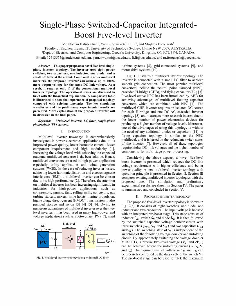
The proposed five-level inverter topology is shown inFig. 2(a). It consists of eight switches, one diode, oneinductor and two capacitors. The input voltage is boostedwith an integrated pre-boost stage. This stage consists ofinductor , switch and diode . It is then followedby the switched capacitor voltage doubler circuit withthree switches ( , and ) and two capacitors (and ). The switching state of is independent of theswitching of the following voltage doubler and unfoldingcircuit. By appropriately switching the voltage doublerMOSFETs, a precise two-level voltage ( and 2 )can be achieved before the unfolding circuit ( , ,and ). The required level of voltage in and canbe precisely controlled by the duty cycle of the switch .The pre-boost stage can be used to track the maximumFig. 1. Multilevel inverter topology along with small LC filter.
power point (MPP) of the PV panel, thereby facilitatingan integrated and compact solution for grid connected PVsystems.
As shown in Fig. 2(b), switching signals are generatedby comparing four carrier signals with one referencesignal. The proposed inverter circuit is capable togenerate five levels of output voltages as +4 Vdc, +2 Vdc,0, −4 Vdc, and −2 Vdc (which are defined as + 2, + 1, 0, –1, and – 2 respectively).
Table 1 shows the voltage states relation for differentswitching operation. The operational mode of proposedtopology is described below.
III. OPERATION PRINCIPLE OF PROPOSED TOPOLOGY
Fig.3 illustrates the different operation modes of theinverter. Fig 3(a) and Fig. 3(d) display the zero states atlevel 1 and Fig. 3(e) shows the active states at level 1. Fig.3(c) and Fig. 3(f) illustrate the active state at level 2.These operating modes are appropriately selected tomaintain the five-level voltage at the inverter output, e.g.ABAB for +1 level, BCBC for +2 level, DEDE for -1level and EFEF for -2 level. These states are discussedbelow in brief:
Active state 1 (A): Fig. 3 (a) shows the active state 1.In this mode, switch is conducting; hence the currentflows from the positive side to negative side of theinductor and through the DC link capacitor . As aresult, inductor is charged. On the other hand, AC
current will flow through the switch and antiparalleldiode of switch .
Active state 2 (B): When turns off, current flowsthrough the switches and while the capacitorand will charge continuously until completing thecycle. Moreover, the current flows into the loadimpedance through and switches for the positivehalf cycle, and the obtained output voltage is +2 Vdc.Fig.3 (b) displays this operation.
Active state 3 (C): In this state (Fig. 3(c)), theswitches and are in the “off” condition. Thecapacitors and are in the discharging mode, andthe discharging path is from the switch to theswitches and for the positive half cycle. Hence, itwill work until discharging is completed. Indeed, theoutput voltage is boosted up to four times.
Active state 4 (D): In zero state for the negative halfcycle as shown in Fig. 3(d), capacitor switched integratedpart is in the “off” condition, and the switch is on. Thecurrent flows through the DC link capacitor and inductor.On the other hand, the input side is fully separated fromthe output side. Hence, the output current flows throughthe switch , and antiparallel diode of switch until thepositive half cycle starts.
Active state 5 (E): In this state (Fig. 3(e)), theswitches and are on, and the capacitors and
are charged continuously until the negative half cycleis completed. Meanwhile, the current flows through theswitches and to the load, and the output voltage isdoubled (-2 Vdc) relative to the input voltage.
Active state 6 (F): Similar to state 3, -2 level in state6 (Fig. 3(f)) is generated when the switches andare in the “off” condition. The capacitors and arein the discharging mode. Moreover, the discharging pathis from the switch to the switches and until thedischarging is completed. As a result, the obtained outputvoltage is four times (-4 Vdc) of the input voltage.
TABLE IOPERATIONAL MODE OF SWITCH WITH VOLTAGE STATES
ModeSwitches Output
VoltageLevel
A 0 0 0 1 0 1 0 0
B 1 0 1 1 0 0 1 1C 0 1 0 1 0 0 1 2D 0 0 0 0 1 0 1 0E 1 0 1 0 1 1 0 −1F 0 1 0 0 1 1 0 −2
S3
S4
S1
S2
vac
PV
Vdc
Cin
SB SC1SC2
SC3CS1
CS2
LB DB
t
AB
BC
BA
DE
EF
ED
-4Vdc
0
4Vdc
Modulation reference
2Vdc
2Vdc-
Carrier Signal
t
Figure 2. Illustration of (a) the proposed 5-level switched-capacitor single-phase boost inverter, and (b) its required modulation technique.

IV. COMPARISON WITH EXISTING TOPOLOGIES
A Multilevel inverter is a high-efficiency basedinverter with less total harmonic distortion (THD).However, the main issue is that more power devices areused; hence, the inverter cost, as well as maintenancecosts, are increased. Table II below illustrates thecomparison of different single-phase multilevel invertertopologies based on the input voltage and power devices.The NPC five-level inverter needs eight power switchesand four diodes to achieve five voltage levels, whileANPC and t-type five-level inverter do not need anydiodes. Instead, they require additional capacitors. All ofthese three topologies need 800 Vdc to produce the 230V AC signal. The common five-level inverters, such asdiode clamped, FC and CHB are constructed by eightpower switches; however, the diode clamped needs extrafour capacitors and 12 diodes to achieve five levels ofvoltage. Table II tabulates the component list of differentcircuits together with the required number ofcomponents for the circuits. All topologies need 400 VDC to achieve the 230 V AC grid voltage. On the otherhand, the proposed topology needs only 110 Vdc inputvoltage with one diode, one inductor, two capacitors andeight power switches.
S3
S4
S1
S2
vac
PV
Vdc
Cin
SB SC1SC2
SC3CS1
CS2
LB DB
S3
S4
S1
S2
vac
PV
Vdc
Cin
SB SC1SC2
SC3CS1
CS2
LB DB
S3
S4
S1
S2
vac
PV
Vdc
Cin
SB SC1SC2
SC3CS1
CS2
LB DB
S3
S4
S1
S2
vac
PV Cin
SB SC1SC2
SC3CS1
CS2
LB DB
S3
S4
S1
S2
vac
PV
Vdc
Cin
SB SC1SC2
SC3CS1
CS2
LB DB
S3
S4
S1
S2
vac
PV
Vdc
Cin
SB SC1SC2
SC3CS1
CS2
LB DB
(a)
(b)
(c)
(d)
(e)
(f)Fig. 3. Operational modes (a) mode A, (b) mode B, (c) mode C, (d) mode D, (e) mode E (f) mode F.
TABLE IICOMPARISON BETWEEN VARIOUS SINGLE-PHASE FIVE LEVEL
INVERTER TOPOLOGIES [11-23].
NameDC InputVoltage
(Vdc)
SemiconductorDevices Additional Devices
Diode Switch Inductor CapacitorNPC 800 4 8 0 0ANPC 800 0 8 0 1T type 800 0 8 0 4Diodeclamped 400 12 8 0 4
Flyingcapacitor 400 0 8 0 10
Cascaded H-bridge 400 0 8 0 0
Topology in[11] 400 2 8 0 0
Topology in[18] [19] 400 8 6 0 0
Topology in[20] 400 6 11 0 1
Topology in[21] 400 0 6 0 3
Topology in[22] 400 1 9 1 2
Topology in[23] 400 0 9 0 3
ProposedInverter 110 1 8 1 2

V. SIMULATION AND EXPERIMENT RESULTS
Simulations have been carried out in MATLAB-Simulink using the PLECS toolbox to analyze theinverter operation. Table III shows the parameters forsimulation and experimental verification. Simulationresult of the novel multilevel inverter is shown in Fig. 4where the applied input is 110 Vdc and an output of 230Vac, 50 Hz frequency and 1 kW power is achieved. Thisfigure shows the input DC voltage, five-level inverteroutput, output voltage and current after applying thesmall LC filter and the voltage across the capacitors (CS1and CS2). On the other hand, Fig. 5 illustrates the voltageacross the switches.
In the experimental work, a four-layer printed circuitboard (size is 117.221 mm × 114.554 mm) is designed forthe 1 kW prototype implementation. The control signals
for the switches are provided through theTMS320F28335 digital signal processor from TexasInstruments. Fig. 6 displays prototype of the proposedtopology and preliminary result of the proposed inverterfor 10 V DC input and 50 Ω load. It shows the five-leveloutput voltage and the output voltage after LC filter..
In experimental work, the four-layer Printed CircuitBoard (PCB) (size is 117.221 mm × 114.554 mm) hasdesigned for 1 kW prototype implementation. Thecontrol signals for the switches were provided throughthe TMS320F28335 digital signal processor (DSP) fromTexas Instruments (TI). In Fig. 6 displays the prototypeof the proposed topology and the preliminary result of theproposed inverter for 10 Vdc input with 50 Ω load whereshows the capability of generating a five-level inverteroutput voltage and the output voltage after LC filter.
VI. CONCLUSION AND FUTURE WORK
In this paper, a novel single-phase 5-level inverter forPV systems is proposed. This topology reduces the DC-link voltage requirement to 1/8 of the conventionalmultilevel (FC, CHB, NPC, ANPC) and ¼ of theconventional H-bridge topologies. Operational mode ofthe proposed topology is discussed briefly. Experimentalsetup of the proposed circuit is constructed, and thepreliminary waveform of the 5-level inverter output isachieved. Finally, simulation waveforms of the proposedtopology are shown for the experimental setup, and thepreliminarily 5-level inverter is achieved for the low input
Fig. 4. Output Voltage and Current waveforms of the proposed5-level inverter with voltage across the capacitors.
TABLE IIIPARAMETERS AND COMPONENTS USED FOR SIMULATION AND
PROTOTYPE DESIGN.
Parameter/ component Values used forsimulation
Values used forExperiment
DC link Capacitor (Cin) 680 µF 680 µF(LLS2E681MELA)
Switching Frequency(Fsw) 15 kHz 15 kHz
Line frequency 50 Hz 50 HzBoost Inductor (Lb) 0.9 mH 0.9 mHBoost Diode (Db) - C5D50065DSwitched Capacitors(CS1 and CS2) 680 µF 680 µF
(LLS2E681MELA)Switches (Sb, SC1, SC2,SC3, S1, S2, S3 and S4) - SCT3022ALGC11
Filter inductor (Lf) 0.40 mH 0.60 mHFilter Capacitor (Cf) 4.7 µF 4.7 µFController - TMS320F28335 DSP
Fig. 5. Voltage across the power switches of the proposed 5-levelinverter.

voltage. In the final version of the paper, more analysisand experimental results will be included with thermalmodeling for calculating losses through semiconductordevices and efficiency evaluation.
REFERENCES
[1] R. Haura, & M. M. Casaro, “Single-phase dual-stage isolatedmultilevel inverter applied to solar energy processing”, 83thIEEE Int. Symposium on Power Electronics for DistributedGeneration Systems (PEDG), Florianópolis, Apr. 2017, pp. 1-8.
[2] A. Choudhury, P. Pillay, & S. S. Williamson, “A performancecomparison study of space-vector and carrier-based PWMtechniques for a 3-level neutral point clamped (NPC) tractioninverter drive”, IEEE Power Electronics, Drives and EnergySystems (PEDES), Mumbai, Dec. 2014, pp. 1-6.
[3] S. Kouro, M. Malinowski, k. Gopakumar, J. Pou, L. G.Franquelo, B. Wu, J. Rodriguez, M. A. Perez & J. I. Leon,“Recent advances and industrial applications of multilevelconverters”, IEEE trans ind. electron., vol. 57, no. 8, pp. 2553-2580, Jun. 2010.
[4] J. Rodriguez, L. G. Franquelo, S. Kouro, J. I. Leon, R. C. Portillo,M. A. M. Prats & M. A. Perez, “Multilevel converters: Anenabling technology for high-power applications”, Proceedingsof the IEEE, vol. 97, no. 11, pp. 1786-1817, Oct. 2009.
[5] S. R. Raman, Y. Ye, & K. E. Cheng, “Switched-capacitormultilevel inverters for high frequency AC microgrids”, IEEEapplied power electron. conf. exp. (APEC), Tampa, FL, Mar.2017, pp. 2559-2564.
[6] Z. Ye, L. Jiang, Z. Zhang, D. Yu, Z. Wang, X. Deng & T.Fernando, “A novel DC-power control method for cascaded H-bridge multilevel inverter”, IEEE trans. ind. electron., vol. 64,no. 9, pp. 6874-6884, Mar. 2017.
[7] S. Rahman, M. Meraj, A. Iqbal, M. Tariq, A. I. Maswood, L. Ben-Brahim & R. Alammari, “Cascaded multilevel qZSI poweredsingle-phase induction motor for water pump application”,IEEE energy conver. congress exp. (ECCE),Cincinnati, OH,Oct. 2017, pp. 1037-1042.
[8] V. Yaramasu, & B. Wu, “Predictive control of a three-level boostconverter and an NPC inverter for high-power PMSG-basedmedium voltage wind energy conversion systems,” IEEE trans.power electron., vol. 29, no. 10, pp. 5308-5322, Oct. 2014.
[9] L. Wang, D. Zhang, Y. Wang, B. Wu, & H. S. Athab, “Power andvoltage balance control of a novel three-phase solid-statetransformer using multilevel cascaded H-bridge inverters formicrogrid applications,” IEEE trans. power electron., vol. 31, no.4, pp. 3289-3302, Apr. 2016.
[10] J. Mathew, K. Mathew, N. A. Azeez, P. P. Rajeevan, & K.Gopakumar, “A hybrid multilevelinverter system based ondodecagonal space vectors for medium voltage IM drives,” IEEEtrans. power electron., vol. 28, no. 8, pp. 3723-3732, Aug. 2013.
[11] M. Sarbanzadeh, M.A-Hosseinzadeh, & E. Sarbanzadeh, “Newfundamental multilevel inverter with reduced number ofswitching elements,” IEEE southern power electron. Conf.(SPEC), Puerto Varas, Dec. 2017, pp: 1-6.
[12] J.S. Lai, & F.Z. Peng, 1996. “Multilevel Converters – A NewBreed of Power Converters”, IEEE trans. Ind. Appl. Vol. 32, no.3, May-June 1996, pp. 509-517.
[13] P. Barbosa, P. Steimer, J. Steinke, M. Winkelnkemper, N.Celanovic, "Active-neutral-point-clamped (ANPC) multilevelconverter technology." IEEE european Conf. power electron.Appl., 2005 pp. 10-pp., 2005.
[14] A. S. M. Salem, “Design and Analysis of Five-Level T-TypePower Converters for Rotating Field Drives,” Ghent University,2015.
[15] A. Nabae, I Takashashi, & H. Akagi, “ A new neutral –pointclamped PWM inverter,” IEEE trans. ind appl., Vol. No. IA-17,pp. 518- 523, Sept/oc 1981.
[16] R. H. Baker and L. H. Bannister, “Electric Power Converter,”U.S. Patent 3 867 643, Feb. 1975.
[17] K. Corzine, & Y. Familiant, “A new cascaded multilevel H-bridge drive,” IEEE trans. power electron., vol. 17, no. 1, pp.125-131, 2002.
[18] E. Babaei, S. Alilu, & S. Laali, “A New General Topology forCascaded Multilevel Inverters With Reduced Number ofComponents Based on Developed H-Bridge,” IEEE trans. Ind.Electron., vol.61, no. 8, pp. 3932-3939, 2014.
[19] E. Babaei, S. Laali, & S. Alilu, “Cascaded Multilevel InverterWith Series Connection of Novel H-Bridge Basic Units,” IEEEtrans. Ind. Electron., vol. 61, no. 12, pp. 6664-6671, 2014.
[20] G. D. Prasad, V. Jegathesan, & P. R. Rao, “Hybrid multilevel DClink inverter with reduced power electronic switches,” Energyprocedia, vol. 117, PP. 626-634, 2017.
[21] C. Bin, W. Yao, & Z. Lu, "Novel five-level three-phase hybrid-clamped converter with reduced components." J. powerelectron. Vol. 14, no. 6, pp. 1119-1129, 2014.
[22] M. Avinash, “Integrated DC-DC converter based High EfficientFive Level Single-Phase Grid-Connected TransformerlessPhotovoltaic Inverter,” M. Tech. Thesis, Indian institute oftechnology kanpur, 2016.
[23] M. Norambuena, S. Kouro, S. Dieckerhoff, & J. Rodriguez,“Reduced multilevel converter: A novel multilevel converterwith a reduced number of active switches,” IEEE trans. ind.electron., vol. 65, no. 5, pp.3636-3645, may 2018
Fig. 6. Hardware setup for a 1 kW prototype of the new inverter (note: switches SCS1, SCS3 and eight gate drive circuits are on the bottom ofthe PCB), and the preliminary waveforms of the 5-level inverter (20 V/ div).


![2018 IEEE. Personal use of this material is permitted. Permission … · 2020-03-14 · consensus control [17]-[20], sampling and injecting synchronization signal [13], or computational-based](https://img.pdfslide.us/doc/110x75/5e98fe9d83dbcb69bd7cc141/2018-ieee-personal-use-of-this-material-is-permitted-permission-2020-03-14-consensus.jpg)


![© 2011 IEEE. Personal use of this material is permitted ... · INDEX TERMS: H.1 [MODELS AND PRINCIPLES]: User/Machine Systems – Human factors, Human information processing; H.5.2](https://img.pdfslide.us/doc/110x75/5f0c06187e708231d433603d/-2011-ieee-personal-use-of-this-material-is-permitted-index-terms-h1-models.jpg)


![c IEEE. Personal use of this material is permitted ...wavelab.at › papers › Jalilian18b.pdf · [13], Principal Component Analysis (PCA [7]), etc. For a general overview on finger-vein](https://img.pdfslide.us/doc/110x75/5f03b3177e708231d40a56bf/c-ieee-personal-use-of-this-material-is-permitted-a-papers-a-jalilian18bpdf.jpg)