Embed Size (px)
Citation preview

ILI9881C
Amorphous TFT LCD Single-Chip Driver
800(RGB) x 1280 Resolution, 16.7M-color
Without Internal GRAM
Specification
Version: V092 Document No: ILI9881C_IDT_V092_20141105
ILI TECHNOLOGY CORP. 8F, No. 38, Taiyuan St, Jhubei City, Taiwan 302, R.O.C. Tel.886-3-5600099; Fax.886-3-5600585 http://www.ilitek.com
a-Si TFT LCD Single Chip Driver 800(RGB) x 1280 Resolution and 16.7M-color ILI9881C
The information contained herein is the exclusive property of ILI Technology Corp. and shall not be distributed, reproduced, or disclosed in whole or in part without prior written permission of ILI Technology Corp. Page 2 of 320
Table of Contents
1. INTRODUCTION ........................................................................................................................................................ 17
2. FEATURES ................................................................................................................................................................. 18
3. DEVICE OVERVIEW .................................................................................................................................................... 20
3.1. BLOCK DIAGRAM ......................................................................................................................................................... 20
3.2. BLOCK FUNCTION DESCRIPTION ...................................................................................................................................... 21
3.2.1. System Interface ................................................................................................................................................. 21
3.2.2. Grayscale Voltage Generating Circuit ................................................................................................................ 21
3.2.3. TCON ................................................................................................................................................................... 21
3.2.4. OSC ..................................................................................................................................................................... 21
3.2.5. RAM .................................................................................................................................................................... 21
3.2.6. Source Driver Circuit ........................................................................................................................................... 21
3.2.7. Gate Controller Circuit ........................................................................................................................................ 21
3.2.8. DC-to-DC Power Supply Circuit ........................................................................................................................... 21
3.2.9. CABC (Content Adaptive Brightness Control) ..................................................................................................... 21
3.3. PIN DESCRIPTIONS ........................................................................................................................................................ 22
3.4. PIN ASSIGNMENT ......................................................................................................................................................... 26
3.5. BUMP ARRANGEMENT .................................................................................................................................................. 27
3.6. PAD COORDINATION ..................................................................................................................................................... 29
4. SYSTEM INTERFACE ................................................................................................................................................... 37
4.1. DSI SYSTEM INTERFACE ................................................................................................................................................. 37
4.1.1. General Description ............................................................................................................................................ 37
4.1.2. Interface Level Communication .......................................................................................................................... 39
4.1.2.1. General .......................................................................................................................................................................39
4.1.2.2. DSI CLK Lanes ..............................................................................................................................................................40
4.1.2.2.1. Low Power Mode (LPM) ........................................................................................................................................40
4.1.2.2.2. Ultra-Low Power Mode (ULPM) ............................................................................................................................42
4.1.2.2.3. High-Speed Clock Mode (HSCM) ...........................................................................................................................43
4.1.2.3. DSI Data Lanes ............................................................................................................................................................46
4.1.2.3.1. General ..................................................................................................................................................................46
4.1.2.3.2. Escape Modes........................................................................................................................................................46
4.1.2.3.2.1. Low-Power Data Transmission (LPDT) ...........................................................................................................48
4.1.2.3.2.2. Ultra-Low Power State (ULPS)........................................................................................................................49
4.1.2.3.2.3. Remote Application Reset (RAR) ....................................................................................................................50
4.1.2.3.2.4. Acknowledge (ACK) ........................................................................................................................................51
4.1.2.3.3. High-Speed Data Transmission (HSDT) ..................................................................................................................52
4.1.2.3.3.1. Entering High-Speed Data Transmission (TSOT of HSDT) ...............................................................................52

a-Si TFT LCD Single Chip Driver 800(RGB) x 1280 Resolution and 16.7M-color ILI9881C
The information contained herein is the exclusive property of ILI Technology Corp. and shall not be distributed, reproduced, or disclosed in whole or in part without prior written permission of ILI Technology Corp. Page 3 of 320
4.1.2.3.3.2. Leaving High-Speed Data Transmission (TEOT of HSDT) ................................................................................53
4.1.2.3.3.3. Burst of the High-Speed Data Transmission (HSDT) .......................................................................................54
4.1.2.3.4. Bus Turnaround (BTA) ...........................................................................................................................................58
4.1.3. Packet Level Communication .............................................................................................................................. 59
4.1.3.1. Short Packet (SPa) and Long Packet (LPa) Structures .................................................................................................59
4.1.3.1.1. Bit Order of the Byte on Packets ...........................................................................................................................60
4.1.3.1.2. Byte Order of the Multiple Byte Information on Packets ......................................................................................60
4.1.3.1.3. Packet Header (PH) ...............................................................................................................................................61
4.1.3.1.3.1. Data Identification (DI)...................................................................................................................................62
4.1.3.1.3.1.1. Virtual Channel (VC) ..............................................................................................................................62
4.1.3.1.3.1.2. Data Type (DT) .......................................................................................................................................63
4.1.3.1.3.2. Packet Data (PD) in a Short Packet (SPa) .......................................................................................................65
4.1.3.1.3.3. Word Count (WC) in a Long Packet (LPa) .......................................................................................................67
4.1.3.1.3.4. Error Correction Code (ECC)...........................................................................................................................68
4.1.3.1.4. Packet Data (PD) in a Long Packet (LPa) ................................................................................................................72
4.1.3.1.5. Packet Footer (PF) in a Long Packet (LPa)..............................................................................................................72
4.1.3.2. Packet Transmissions ..................................................................................................................................................74
4.1.3.2.1. Packet from the MCU to the Display Module ........................................................................................................74
4.1.3.2.1.1. Display Command Set (DCS) ..........................................................................................................................74
4.1.3.2.1.2. Display Command Set (DCS) Write, No Parameter (DCSWN-S) .....................................................................75
4.1.3.2.1.3. Display Command Set (DCS) Write, 1 Parameter (DCSW1-S) .........................................................................76
4.1.3.2.1.4. Display Command Set (DCS) Write Long (DCSW-L) ........................................................................................77
4.1.3.2.1.5. Display Command Set (DCS) Read, No Parameter (DCSRN-S) ........................................................................81
4.1.3.2.1.6. Null Packet, No Data (NP-L) ...........................................................................................................................84
4.1.3.2.1.7. End of Transmission Packet (EoTP) ................................................................................................................86
4.1.3.2.2. Packet from the Display Module to the MCU ........................................................................................................88
4.1.3.2.2.1. Used Packet types ..........................................................................................................................................88
4.1.3.2.2.2. Acknowledge with Error Report (AwER) ........................................................................................................89
4.1.3.2.2.3. DCS Read Long Response (DCSRR-L) ..............................................................................................................91
4.1.3.2.2.4. DCS Read Short Response, 1 Byte Returned (DCSRR1-S) ...............................................................................93
4.1.3.2.2.5. DCS Read Short Response, 2 Bytes Returned (DCSRR2-S)..............................................................................94
4.1.3.3. Communication Sequences ........................................................................................................................................95
4.1.3.3.1. General ..................................................................................................................................................................95
4.1.3.3.2. Sequences .............................................................................................................................................................97
4.1.3.3.2.1. DCS Write, 1 Parameter Sequence.................................................................................................................97
4.1.3.3.2.2. DCS Write, No Parameter Sequence ..............................................................................................................98
4.1.3.3.2.3. DCS Write Long Sequence ..............................................................................................................................99
4.1.3.3.2.4. DCS Read, No Parameter Sequence .............................................................................................................100
4.1.3.3.2.5. Null Packet, No Data Sequence ....................................................................................................................102

a-Si TFT LCD Single Chip Driver 800(RGB) x 1280 Resolution and 16.7M-color ILI9881C
The information contained herein is the exclusive property of ILI Technology Corp. and shall not be distributed, reproduced, or disclosed in whole or in part without prior written permission of ILI Technology Corp. Page 4 of 320
4.1.3.3.2.6. End of Transmission Packet .........................................................................................................................102
4.1.3.4. 16 bit / pixel Writing .................................................................................................................................................103
4.1.3.5. 24 bit/pixel Writing ...................................................................................................................................................105
4.2. DISPLAY DATA FORMAT ...............................................................................................................................................107
4.2.1. DSI Transmission Data Format .........................................................................................................................107
4.2.1.1. 16-bit per Pixel, Long Packet, Data Type 00 1110 (0Eh) ...........................................................................................107
4.2.1.2. 18-bit per Pixel, Long Packet, Data Type = 01 1110 (1Eh) ........................................................................................107
4.2.1.3. 18-bit per Pixel, Long Packet, Data Type = 10 1110 (2Eh) ........................................................................................108
4.2.1.4. 24-bit per Pixel, Long Packet, Data Type = 11 1110 (3Eh) ........................................................................................109
4.2.2. 16/18-bit Color Data Mapping to 24-bit Pixel Data Operation ........................................................................111
5. COMMAND ............................................................................................................................................................. 113
5.1. COMMAND FLOW ......................................................................................................................................................113
5.2. COMMAND LIST .........................................................................................................................................................114
5.2.1. Page 0 Command Set .......................................................................................................................................114
5.2.2. Page 1 Command Set .......................................................................................................................................116
5.2.3. Page 2 Command Set .......................................................................................................................................118
5.2.4. Page 3 Command Set .......................................................................................................................................119
5.2.5. Page 4 Command Set .......................................................................................................................................120
5.2.6. Page 5 Command Set .......................................................................................................................................121
5.2.7. Page 6 Command Set .......................................................................................................................................121
5.2.8. Page 7 Command Set .......................................................................................................................................122
5.2.9. Page 8 Command Set .......................................................................................................................................122
5.2.10. Page 9 Command Set ...................................................................................................................................123
5.2.11. Page 10 Command Set .................................................................................................................................123
5.3. PAGE 0 COMMAND DESCRIPTION ..................................................................................................................................124
5.3.1. NOP (00h) .........................................................................................................................................................124
5.3.2. Software Reset (01h) ........................................................................................................................................125
5.3.3. Read Number of the Errors on DSI (05h) ..........................................................................................................126
5.3.4. Read Display Power Mode (0Ah) ......................................................................................................................127
5.3.5. Read Display MADCTL (0Bh) .............................................................................................................................128
5.3.6. Read Display Pixel Format (0Ch) .......................................................................................................................129
5.3.7. Read Display Image Mode (0Dh) ......................................................................................................................130
5.3.8. Read Display Signal Mode (0Eh) .......................................................................................................................131
5.3.9. Read Display Self-Diagnostic Result (0Fh) ........................................................................................................132
5.3.10. Sleep In (10h) ...............................................................................................................................................133
5.3.11. Sleep Out (11h) ............................................................................................................................................134
5.3.12. Normal Display Mode On (13h) ...................................................................................................................135
5.3.13. All Pixel Off (22h) .........................................................................................................................................136
a-Si TFT LCD Single Chip Driver 800(RGB) x 1280 Resolution and 16.7M-color ILI9881C
The information contained herein is the exclusive property of ILI Technology Corp. and shall not be distributed, reproduced, or disclosed in whole or in part without prior written permission of ILI Technology Corp. Page 5 of 320
5.3.14. All Pixel On (23h) ..........................................................................................................................................137
5.3.15. Gamma Set (26h) .........................................................................................................................................138
5.3.16. Display Off (28h) ..........................................................................................................................................139
5.3.17. Display ON (29h) ..........................................................................................................................................140
5.3.18. Memory Write (2Ch) ....................................................................................................................................141
5.3.19. Tearing Effect Line Off (34h) ........................................................................................................................142
5.3.20. Tearing Effect Line On (35h) ........................................................................................................................143
5.3.21. Memory Access Control (36h) ......................................................................................................................145
5.3.22. Idle Mode Off (38h) ......................................................................................................................................146
5.3.23. Idle Mode On (39h) ......................................................................................................................................147
5.3.24. Interface Pixel Format (3Ah) ........................................................................................................................148
5.3.25. Memory Write Continue (3Ch) .....................................................................................................................149
5.3.26. Set_Tear_Scanline (44h) ..............................................................................................................................150
5.3.27. Get_Tear_Scanline (45h) .............................................................................................................................151
5.3.28. Write Display Brightness Value (51h) ..........................................................................................................152
5.3.29. Read Display Brightness Value (52h) ...........................................................................................................153
5.3.30. Write CTRL Display Value (53h) ...................................................................................................................154
5.3.31. Read CTRL Display Value (54h) ....................................................................................................................155
5.3.32. Write Power Save (55h) ...............................................................................................................................156
5.3.33. Read Power Save (56h) ................................................................................................................................157
5.3.34. Stop Transition (59h) ...................................................................................................................................158
5.3.35. Write CABC Minimum Brightness (5Eh) .......................................................................................................159
5.3.36. Read CABC Minimum Brightness (5Fh) ........................................................................................................160
5.3.37. Set Transition Time (68h) .............................................................................................................................161
5.3.38. Get Transition Time (69h) ............................................................................................................................163
5.3.39. Read Black/White Low Bits (70h) ................................................................................................................165
5.3.40. Read Bkx (71h) .............................................................................................................................................166
5.3.41. Read Bky (72h) .............................................................................................................................................167
5.3.42. Read Wx (73h) .............................................................................................................................................168
5.3.43. Read Wy (74h) .............................................................................................................................................169
5.3.44. Read Red/Green Low Bits (75h) ...................................................................................................................170
5.3.45. Read Rx (76h) ...............................................................................................................................................171
5.3.46. Read Ry (77h) ...............................................................................................................................................172
5.3.47. Read Gx (78h) ..............................................................................................................................................173
5.3.48. Read Gy (79h) ..............................................................................................................................................174
5.3.49. Read Blue/A Color Low Bits (7Ah) ................................................................................................................175
5.3.50. Read Bx (7Bh)...............................................................................................................................................176
5.3.51. Read By (7Ch) ...............................................................................................................................................177
5.3.52. Read Ax (7Dh) ..............................................................................................................................................178
a-Si TFT LCD Single Chip Driver 800(RGB) x 1280 Resolution and 16.7M-color ILI9881C
The information contained herein is the exclusive property of ILI Technology Corp. and shall not be distributed, reproduced, or disclosed in whole or in part without prior written permission of ILI Technology Corp. Page 6 of 320
5.3.53. Read Ay (7Eh) ...............................................................................................................................................179
5.3.54. Write Idle Mode Color (80h) ........................................................................................................................180
5.3.55. Read Idle Mode Color (81h) .........................................................................................................................181
5.3.56. Read DDB Start (A1h) ..................................................................................................................................182
5.3.57. Read DDB Continue (A8h) ............................................................................................................................184
5.3.58. Read First Checksum (AAh) ..........................................................................................................................185
5.3.59. Read Continue Checksum (AFh) ...................................................................................................................186
5.3.60. Read ID1 (DAh) ............................................................................................................................................187
5.3.61. Read ID2 (DBh).............................................................................................................................................188
5.3.62. Read ID3 (DCh) .............................................................................................................................................189
5.3.63. EXTC Command Set Enable Register (FFh) ...................................................................................................190
5.4. PAGE 1 COMMAND DESCRIPTION ..................................................................................................................................191
5.4.1. Read ID4 (00h~02h) ..........................................................................................................................................191
5.4.2. Set Panel Operation Mode and Data Complement Setting (22h) .....................................................................192
5.4.3. Blanking Porch Control (25h~28h) ....................................................................................................................193
5.4.4. Touch Synchronization Control (29h) ...............................................................................................................194
5.4.5. Gate Number (2Eh) ...........................................................................................................................................195
5.4.6. Display Inversion Control (31h).........................................................................................................................196
5.4.7. Dithering Enable (34h) ......................................................................................................................................198
5.4.8. Pump Clock Adjustment (40h~43h) ..................................................................................................................199
5.4.9. Power Control 1 (50h~51h)...............................................................................................................................201
5.4.10. VCOM Control 1 (52h~56h) ..........................................................................................................................203
5.4.11. Entry Mode Set (58h) ...................................................................................................................................204
5.4.12. Source Timing Adjust (60h~63h) ..................................................................................................................205
5.4.13. Positive Gamma Correction (A0h~B3h) .......................................................................................................206
5.4.14. Pad Control (B6h~B7h) ................................................................................................................................207
5.4.15. Negative Gamma Correction (C0h~D3h) .....................................................................................................208
5.4.16. NV Memory Write (E0h~E2h) ......................................................................................................................209
5.4.17. NV Memory Protection Key (E3h~E5h) ........................................................................................................210
5.4.18. NV Memory Status Read (E6h~E9h) ............................................................................................................211
5.4.19. Time Stamp (F0h~F1h) .................................................................................................................................213
5.4.20. EXTC Command Set Enable Register (FFh) ...................................................................................................214
5.5. PAGE 2 COMMAND DESCRIPTION ..................................................................................................................................215
5.5.1. Dynamic Backlight Control 1 (03h~05h) ...........................................................................................................215
5.5.2. Dynamic Backlight Control 2 (06h~07h) ...........................................................................................................216
5.5.3. IIE Function Control (10h~19h) .........................................................................................................................217
5.5.4. IIE Saturation Enhancement Control 1 (1Ah~1Ch) ............................................................................................219
5.5.5. IIE Saturation Protection Control (40h~4Fh).....................................................................................................220
5.5.6. IIE Sharpness Enhancement Control (5Ah~5Ch) ...............................................................................................222

a-Si TFT LCD Single Chip Driver 800(RGB) x 1280 Resolution and 16.7M-color ILI9881C
The information contained herein is the exclusive property of ILI Technology Corp. and shall not be distributed, reproduced, or disclosed in whole or in part without prior written permission of ILI Technology Corp. Page 7 of 320
5.5.7. IIE Contrast Enhancement Control (60h~66h) ..................................................................................................223
5.5.8. EXTC Command Set Enable Register (FFh) ........................................................................................................224
5.6. PAGE 3 COMMAND DESCRIPTION ..................................................................................................................................225
5.6.1. EXTC Command Set Enable Register (FFh) ........................................................................................................225
5.7. PAGE 4 COMMAND DESCRIPTION ..................................................................................................................................226
5.7.1. DSI Lanes Control (00h) ....................................................................................................................................226
5.7.2. Touch Synchronization Timing Adjust (27h~2Ah) .............................................................................................227
5.7.3. BIST Mode Function (2Dh,2Fh) .........................................................................................................................229
5.7.4. Power Control 1 (69h) .......................................................................................................................................230
5.7.5. VCORE Setting (6Ch) .........................................................................................................................................231
5.7.6. Power Control 2 (6Eh) .......................................................................................................................................232
5.7.7. Power Control 3 (6Fh) .......................................................................................................................................233
5.7.8. VCOM Control (8Bh) .........................................................................................................................................235
5.7.9. Power Control 4 (8Ch~8Dh) ..............................................................................................................................236
5.7.10. Temperature Detecting Setting (BBh~CEh) ..................................................................................................238
5.7.11. OTP Control (D7h) ........................................................................................................................................241
5.7.12. EXTC Command Set Enable Register (FFh) ...................................................................................................242
5.8. PAGE 5 COMMAND DESCRIPTION ..................................................................................................................................243
5.8.1. Fine Digital Gamma Control 1 (00h~7Fh) .........................................................................................................243
5.8.2. Digital 3 Gamma Enable (80h) .........................................................................................................................245
5.8.3. EXTC Command Set Enable Register (FFh) ........................................................................................................246
5.9. PAGE 6 COMMAND DESCRIPTION ..................................................................................................................................247
5.9.1. Fine Digital Gamma Control 2 (00h~7Fh) .........................................................................................................247
5.9.2. EXTC Command Set Enable Register (FFh) ........................................................................................................249
5.10. PAGE 7 COMMAND DESCRIPTION ..................................................................................................................................250
5.10.1. Fine Digital Gamma Control 3 (00h~7Fh) ....................................................................................................250
5.10.2. EXTC Command Set Enable Register (FFh) ...................................................................................................252
5.11. PAGE 8 COMMAND DESCRIPTION ..................................................................................................................................253
5.11.1. Fine Digital Gamma Control 4 (00h~7Fh) ....................................................................................................253
5.11.2. EXTC Command Set Enable Register (FFh) ...................................................................................................255
5.12. PAGE 9 COMMAND DESCRIPTION ..................................................................................................................................256
5.12.1. Fine Digital Gamma Control 5 (00h~7Fh) ....................................................................................................256
5.12.2. EXTC Command Set Enable Register (FFh) ...................................................................................................258
5.13. PAGE 10 COMMAND DESCRIPTION ................................................................................................................................259
5.13.1. Fine Digital Gamma Control 6 (00h~7Fh) ....................................................................................................259
5.13.2. EXTC Command Set Enable Register (FFh) ...................................................................................................261
6. SOURCE DRIVER ...................................................................................................................................................... 262
6.1. ZIG-ZAG INVERSION ....................................................................................................................................................262
a-Si TFT LCD Single Chip Driver 800(RGB) x 1280 Resolution and 16.7M-color ILI9881C
The information contained herein is the exclusive property of ILI Technology Corp. and shall not be distributed, reproduced, or disclosed in whole or in part without prior written permission of ILI Technology Corp. Page 8 of 320
6.2. ZIG-ZAG INVERSION CONCEPT .......................................................................................................................................263
6.3. ZIG-ZAG INVERSION SOURCE OUTPUT METHOD ...............................................................................................................264
6.4. ZIG-ZAG INVERSION RED DATA DISPLAY .........................................................................................................................265
6.5. ZIG-ZAG INVERSION GREEN DATA DISPLAY ....................................................................................................................266
6.6. ZIG-ZAG INVERSION BLUE DATA DISPLAY .......................................................................................................................267
6.7. DIFFERENT ZIG-ZAG TYPE PANEL ...................................................................................................................................268
7. ENTER/EXIT IDLE MODE FLOW ................................................................................................................................ 270
7.1. ENTER/EXIT IDLE MODE FLOW .....................................................................................................................................270
7.2. ENTER/EXIT IDLE MODE SEQUENCE ...............................................................................................................................271
8. BIST MODE FUNCTION ............................................................................................................................................ 272
8.1. BIST MODE PATTERN .................................................................................................................................................272
9. CONTENT ADAPTIVE BRIGHTNESS CONTROL (CABC) FUNCTION ............................................................................. 273
10. COLOR ENHANCEMENT FUNCTION ..................................................................................................................... 274
10.1. SATURATION ENHANCEMENT .......................................................................................................................................274
10.2. CONTRAST ENHANCEMENT ..........................................................................................................................................276
10.3. SHARPNESS ENHANCEMENT .........................................................................................................................................277
10.4. SUNLIGHT READABILITY ...............................................................................................................................................278
11. SLEEP OUT COMMAND AND SELF-DIAGNOSTIC FUNCTIONS .............................................................................. 279
11.1. REGISTER LOADING DETECTION .....................................................................................................................................279
11.2. FUNCTIONALITY DETECTION .........................................................................................................................................280
12. POWER ON/OFF SEQUENCE ............................................................................................................................... 281
12.1. POWER ON/OFF SEQUENCE ..........................................................................................................................................281
12.1.1. Power Mode 2A ...........................................................................................................................................281
12.1.2. Power Mode 3 ..............................................................................................................................................282
12.1.3. Power Mode 4 ..............................................................................................................................................283
12.2. UNCONTROLLED POWER OFF .......................................................................................................................................284
13. POWER LEVEL DEFINITION ................................................................................................................................. 285
13.1. POWER LEVELS ..........................................................................................................................................................285
13.2. POWER FLOW CHART..................................................................................................................................................285
14. CHARACTERISTICS OF I/O ................................................................................................................................... 286
14.1. OUTPUT OR BI-DIRECTIONAL (I/O) PINS .........................................................................................................................286
14.2. INPUT PINS ...............................................................................................................................................................286
15. NV MEMORY PROGRAMMING FLOW ................................................................................................................. 287
a-Si TFT LCD Single Chip Driver 800(RGB) x 1280 Resolution and 16.7M-color ILI9881C
The information contained herein is the exclusive property of ILI Technology Corp. and shall not be distributed, reproduced, or disclosed in whole or in part without prior written permission of ILI Technology Corp. Page 9 of 320
15.1. EXTERNAL MTP_PWR PROGRAMMING FLOW ................................................................................................................287
15.2. INTERNAL VGH PROGRAMMING FLOW ..........................................................................................................................288
16. GAMMA CORRECTION ........................................................................................................................................ 289
17. TOUCH SYNCHRONIZATION SIGNAL ................................................................................................................... 290
18. ELECTRICAL CHARACTERISTICS ........................................................................................................................... 291
18.1. ABSOLUTE MAXIMUM RATINGS (TBD) ..........................................................................................................................291
18.2. DC CHARACTERISTICS FOR PANEL DRIVING......................................................................................................................292
18.3. DSI DC CHARACTERISTICS ...........................................................................................................................................293
18.3.1. DC Characteristics for Power Lines ..............................................................................................................293
18.3.2. DC Characteristics for DSI LP Mode .............................................................................................................294
18.3.3. Spike/Glitch Rejection ..................................................................................................................................294
18.3.4. DC Characteristics for DSI HS mode .............................................................................................................295
18.4. AC CHARACTERISTICS ..................................................................................................................................................298
18.4.1. DSI Timing Characteristics ...........................................................................................................................298
18.4.2. High Speed Mode – Clock Channel Timing ...................................................................................................298
18.4.3. High Speed Mode – Data Clock Channel Timing ..........................................................................................299
18.4.4. High Speed Mode – Rising and Falling Timings ...........................................................................................300
18.4.5. Low Speed Mode – Bus Turn Around ...........................................................................................................301
18.4.6. Data Lanes from Low Power Mode to High Speed Mode ............................................................................302
18.4.7. Data Lanes from High Speed Mode to Low Power Mode ............................................................................303
18.4.8. DSI Clock Burst – High Speed Mode to/from Low Power Mode ...................................................................304
18.4.9. Timing for DSI video mode ...........................................................................................................................305
18.4.10. Reset Timing ................................................................................................................................................307
19. PANEL APPLICATION .......................................................................................................................................... 308
19.1. INPUT POWER TYPE ....................................................................................................................................................308
19.2. POWER MODE 2A (BOOSTM[2:0] = 1H, DI_PWR_REG = 0H) ......................................................................................309
19.2.1. Power Structure ...........................................................................................................................................309
19.2.2. Reference Circuit ..........................................................................................................................................310
19.2.3. External Component ....................................................................................................................................311
19.3. POWER MODE 3 (BOOSTM[2:0] = 2H, DI_PWR_REG = DON’T CARE) ............................................................................312
19.3.1. Power Structure ...........................................................................................................................................312
19.3.2. Reference Circuit ..........................................................................................................................................313
19.3.3. External Component ....................................................................................................................................314
19.4. POWER MODE 4 (BOOSTM[2:0] = 1H, DI_PWR_REG = 1H) ........................................................................................315
19.4.1. Power Structure ...........................................................................................................................................315
19.4.2. Reference Circuit ..........................................................................................................................................316
19.4.3. External Component ....................................................................................................................................317

a-Si TFT LCD Single Chip Driver 800(RGB) x 1280 Resolution and 16.7M-color ILI9881C
The information contained herein is the exclusive property of ILI Technology Corp. and shall not be distributed, reproduced, or disclosed in whole or in part without prior written permission of ILI Technology Corp. Page 10 of 320
19.5. MAXIMUM LAYOUT RESISTANCE (TBD) .........................................................................................................................318
20. LIQUID CRYSTAL POWER SUPPLY SPECIFICATIONS ............................................................................................. 319
21. REVISION HISTORY ............................................................................................................................................. 320
a-Si TFT LCD Single Chip Driver 800(RGB) x 1280 Resolution and 16.7M-color ILI9881C
The information contained herein is the exclusive property of ILI Technology Corp. and shall not be distributed, reproduced, or disclosed in whole or in part without prior written permission of ILI Technology Corp. Page 11 of 320
List of Figures
FIGURE 1: BLOCK DIAGRAM .............................................................................................................................................................. 20
FIGURE 2: DSI SYSTEM INTERFACE DIAGRAM ....................................................................................................................................... 38
FIGURE 3: CLOCK LANE POWER MODES ............................................................................................................................................... 40
FIGURE 4: FROM ULPM TO LPM ...................................................................................................................................................... 41
FIGURE 5: FROM HIGH SPEED CLOCK MODE (HSCM) TO LPM ............................................................................................................... 41
FIGURE 6: ALL THREE MODE CHANGES TO LPM ................................................................................................................................... 42
FIGURE 7: FROM LPM TO ULPM ...................................................................................................................................................... 42
FIGURE 8: MODE CHANGE FROM LPM TO ULPM................................................................................................................................. 43
FIGURE 9: FROM LPM TO HSCM ...................................................................................................................................................... 43
FIGURE 10: MODE CHANGE FROM LPM TO HSCM .............................................................................................................................. 44
FIGURE 11: HIGH SPEED CLOCK BURST ............................................................................................................................................... 45
FIGURE 12 GENERAL ESCAPE MODE SEQUENCE .................................................................................................................................... 47
FIGURE 13: LOW-POWER DATA TRANSMISSION (LPDT) ........................................................................................................................ 48
FIGURE 14: PAUSE (EXAMPLE) .......................................................................................................................................................... 48
FIGURE 15: ULTRA-LOW POWER STATE (ULPS) ................................................................................................................................... 49
FIGURE 16: REMOTE APPLICATION RESET (RAR) .................................................................................................................................. 50
FIGURE 17: ACKNOWLEDGE (ACK) .................................................................................................................................................... 51
FIGURE 18: ENTERING HIGH-SPEED DATA TRANSMISSION (TSOT OF HSDT) ............................................................................................. 52
FIGURE 19: LEAVING HIGH-SPEED DATA TRANSMISSION (TEOT OF HSDT) ............................................................................................... 53
FIGURE 20: SINGLE PACKET IN HIGH-SPEED DATA TRANSMISSIONS .......................................................................................................... 54
FIGURE 21: MULTIPLE PACKETS IN HIGH-SPEED DATA TRANSMISSION – EXAMPLES ..................................................................................... 54
FIGURE 22: NUMBER OF BYTES, N, TRANSMITTED IS AN INTEGER MULTIPLE OF THE NUMBER OF LANES ............................................................ 54
FIGURE 23: NUMBER OF BYTES, N, TRANSMITTED IS NOT AN INTEGER MULTIPLE OF THE NUMBER OF LANES (EXAMPLE 1) ................................. 55
FIGURE 24: NUMBER OF BYTES, N, TRANSMITTED IS NOT AN INTEGER MULTIPLE OF THE NUMBER OF LANES (EXAMPLE 2) ................................. 55
FIGURE 25: NUMBER OF BYTES, N, TRANSMITTED IS NOT AN INTEGER MULTIPLE OF THE NUMBER OF LANES (EXAMPLE 3) ................................. 55
FIGURE 26: CONTINUOUS MULTIPLE PACKETS IN HSDT WHEN NUMBER OF BYTES IS EQUAL ON DATA LANES AT THE END OF THE PACKET ............ 56
FIGURE 27: CONTINUOUS MULTIPLE PACKETS IN HSDT WHEN NUMBER OF BYTES IS NOT EQUAL ON DATA LANES AT THE END OF THE PACKET
(EXAMPLE 1) ........................................................................................................................................................................ 56
FIGURE 28: CONTINUOUS MULTIPLE PACKETS IN HSDT WHEN NUMBER OF BYTES IS NOT EQUAL ON DATA LANES AT THE END OF THE PACKET
(EXAMPLE 2) ........................................................................................................................................................................ 56
FIGURE 29: CONTINUOUS MULTIPLE PACKETS IN HSDT WHEN NUMBER OF BYTES IS NOT EQUAL ON DATA LANES AT THE END OF THE PACKET
(EXAMPLE 3) ........................................................................................................................................................................ 57
FIGURE 30: BUS TURNAROUND PROCEDURE ........................................................................................................................................ 58
FIGURE 31: SHORT PACKET (SPA) STRUCTURE ...................................................................................................................................... 59
FIGURE 32: LONG PACKET (LPA) STRUCTURE ....................................................................................................................................... 59
FIGURE 33: BIT ORDER OF THE BYTE ON PACKETS ................................................................................................................................. 60
FIGURE 34: BYTE ORDER OF THE MULTIPLE BYTE INFORMATION ON PACKETS............................................................................................. 60
FIGURE 35: PACKET HEADER (PH) IN A SHORT PACKET (SPA) ................................................................................................................. 61
a-Si TFT LCD Single Chip Driver 800(RGB) x 1280 Resolution and 16.7M-color ILI9881C
The information contained herein is the exclusive property of ILI Technology Corp. and shall not be distributed, reproduced, or disclosed in whole or in part without prior written permission of ILI Technology Corp. Page 12 of 320
FIGURE 36: PACKET HEADER (PH) IN A LONG PACKET (LPA) ................................................................................................................... 61
FIGURE 37: DATA IDENTIFICATION (DI) STRUCTURE............................................................................................................................... 62
FIGURE 38: DATA IDENTIFICATION (DI) ON THE PACKET HEADER (PH) ...................................................................................................... 62
FIGURE 39: VIRTUAL CHANNEL (VC) ON THE PACKET HEADER (PH) ......................................................................................................... 62
FIGURE 40: VIRTUAL CHANNEL (VC) CONFIGURATION ........................................................................................................................... 63
FIGURE 41: DATA TYPE (DT) ON THE PACKET HEADER (PH) ................................................................................................................... 63
FIGURE 42: PACKET DATA (PD) FOR SHORT PACKET (SPA), 2 BYTES INFORMATION .................................................................................... 65
FIGURE 43: PACKET DATA (PD) FOR SHORT PACKET (SPA), 1 BYTE INFORMATION ...................................................................................... 66
FIGURE 44: WORD COUNT (WC) IN A LONG PACKET (LPA) .................................................................................................................... 67
FIGURE 45: PACKET DATA IN SHORT AND LONG PACKETS ....................................................................................................................... 67
FIGURE 46: D [23…0] AND P [7…0] IN A SHORT PACKET (SPA).............................................................................................................. 68
FIGURE 47: D [23…0] AND P [7…0] IN A LONG PACKET (LPA) ............................................................................................................... 68
FIGURE 48: XOR FUNCTION ON A SHORT PACKET (SPA) ........................................................................................................................ 69
FIGURE 49: XOR FUNCTION ON A LONG PACKET (LPA) .......................................................................................................................... 70
FIGURE 50: INTERNAL ERROR CORRECTION CODE (IECC) ON THE DISPLAY MODULE (= THE RECEIVER) ........................................................... 70
FIGURE 51: INTERNAL XOR CALCULATION BETWEEN ECC AND IECC VALUES – NO ERROR ........................................................................... 71
FIGURE 52: INTERNAL XOR CALCULATION BETWEEN ECC AND IECC VALUES - ERROR ................................................................................. 71
FIGURE 53: 16-BIT CYCLIC REDUNDANCY CHECK (CRC) CALCULATION ...................................................................................................... 72
FIGURE 54: CRC CALCULATION – PACKET DATA (PD) IS 01H .................................................................................................................. 72
FIGURE 55: PACKET FOOTER (PF) EXAMPLE ......................................................................................................................................... 73
FIGURE 56: DISPLAY COMMAND SET (DCS) IN SHORT PACKET (SPA) AND LONG PACKET (LPA) .................................................................... 74
FIGURE 57: DISPLAY COMMAND SET (DCS) WRITE, NO PARAMETER (DCSWN-S) - EXAMPLE ..................................................................... 75
FIGURE 58: DISPLAY COMMAND SET (DCS) WRITE, 1 PARAMETER (DCSW1-S) – EXAMPLE ........................................................................ 76
FIGURE 59: DISPLAY COMMAND SET (DCS) WRITE LONG (DCSW-L) WITH DCS ONLY - EXAMPLE ................................................................ 78
FIGURE 60: DISPLAY COMMAND SET (DCS) WRITE LONG WITH DCS AND 1 PARAMETER - EXAMPLE ............................................................. 79
FIGURE 61: DISPLAY COMMAND SET (DCS) WRITE LONG WITH DCS AND 4 PARAMETERS - EXAMPLE ............................................................ 80
FIGURE 62: SET MAXIMUM RETURN PACKET SIZE (SMRPS-S) - EXAMPLE ................................................................................................ 82
FIGURE 63: DISPLAY COMMAND SET (DCS) READ, NO PARAMETER (DCSRN-S) - EXAMPLE ........................................................................ 83
FIGURE 64: NULL PACKET, NO DATA (NP-L) - EXAMPLE ........................................................................................................................ 85
FIGURE 65: END OF TRANSMISSION PACKET (EOTP) .............................................................................................................................. 87
FIGURE 66: END OF TRANSMISSION PACKET (EOTP)-EXAMPLES .............................................................................................................. 87
FIGURE 67: RETURN BYTES IN SINGLE PACKET ...................................................................................................................................... 88
FIGURE 68: RETURN BYTES IN SEVERAL PACKETS – NOT ALLOWED ........................................................................................................... 88
FIGURE 69: EXCEPTION WHEN RETURNED BYTES IN SEVERAL PACKETS ...................................................................................................... 88
FIGURE 70: ACKNOWLEDGE WITH ERROR REPORT (AWER) – EXAMPLE .................................................................................................... 90
FIGURE 71: ERRORS PACKETS ............................................................................................................................................................ 90
FIGURE 72: FLOW CHART FOR ERRORS ON DSI ..................................................................................................................................... 91
FIGURE 73: DCS READ LONG RESPONSE (DCSRR-L) - EXAMPLE ............................................................................................................. 92
FIGURE 74: DCS READ SHORT RESPONSE, 1 BYTE RETURNED (DCSRR1-S) - EXAMPLE ............................................................................... 93

a-Si TFT LCD Single Chip Driver 800(RGB) x 1280 Resolution and 16.7M-color ILI9881C
The information contained herein is the exclusive property of ILI Technology Corp. and shall not be distributed, reproduced, or disclosed in whole or in part without prior written permission of ILI Technology Corp. Page 13 of 320
FIGURE 75: DCS READ SHORT RESPONSE, 2 BYTES RETURNED (DCSRR2-S) - EXAMPLE .............................................................................. 94
FIGURE 76: ONE PIXEL BIT AND WRITE COLOR ORDERS .......................................................................................................................103
FIGURE 77: ONE PIXEL WRITE (DCSW-L) – EXAMPLE 1 ......................................................................................................................103
FIGURE 78: RED / GREEN [0:2] SUBPIXEL WRITE (DCSW1-S) – EXAMPLE 2 ...........................................................................................104
FIGURE 79: GREEN [3:5] / BLUE SUBPIXEL WRITE (DCSW1-S) – EXAMPLE 3 .........................................................................................104
FIGURE 80: ONE PIXEL BIT AND COLOR WRITE ORDERS .......................................................................................................................105
FIGURE 81: ONE PIXEL WRITE (DCSW-L) – EXAMPLE .........................................................................................................................105
FIGURE 82: BLUE SUBPIXEL WRITE (DCSW1-S) – EXAMPLE 2 ..............................................................................................................106
FIGURE 83: GREEN SUBPIXEL WRITE (DCSW1-S) – EXAMPLE 3 ............................................................................................................106
FIGURE 84: RED SUBPIXEL WRITE (DCSW1-S) – EXAMPLE 4 ...............................................................................................................106
FIGURE 85: 16-BIT PER PIXEL, DATA TYPE 00 1110 (0EH) ...................................................................................................................107
FIGURE 86: 18-BIT PER PIXEL, DATA TYPE = 01 1110 (1EH) ................................................................................................................108
FIGURE 87: 18-BIT PER PIXEL, DATA TYPE = 10 1110 (2EH) ................................................................................................................109
FIGURE 88: 24-BIT PER PIXEL, DATA TYPE = 11 1110 (3EH) ................................................................................................................110
FIGURE 89: EPF[1:0] = 10, 16-BIT DATA MAPPING TO 24-BIT ............................................................................................................112
FIGURE 90: EPF[1:0] = 10, 18-BIT DATA MAPPING TO 24-BIT ............................................................................................................112
FIGURE 91: COMMAND FLOW .........................................................................................................................................................113
FIGURE 92: ENTER IDLE MODE FLOW ...............................................................................................................................................270
FIGURE 93: EXIT IDLE MODE FLOW ..................................................................................................................................................270
FIGURE 94: ENTER/EXIT IDLE MODE SEQUENCE .................................................................................................................................271
FIGURE 95: CABC BLOCK DIAGRAM .................................................................................................................................................273
FIGURE 96: PWM OUT ON/OFF PERIOD .........................................................................................................................................273
FIGURE 97: SATURATION ENHANCEMENT (A) HSL MODEL, (B) THE DEFINITION OF 24 COLOR-AXIS. ..............................................................274
FIGURE 98: SATURATION ENHANCEMENT (A) ALL COLOR-AXIS WITH SAME LEVEL, (B) HIGHER LEVEL IN RED-AXIS, (C) HIGHER LEVEL IN GREEN-AXIS (D)
HIGHER LEVEL IN BLUE-AXIS. ...................................................................................................................................................274
FIGURE 99: SATURATION ENHANCEMENT IMAGE (A) ORIGINAL, (B) LOW LEVEL, (C) MEDIUM LEVEL, (D) HIGH LEVEL. ....................................275
FIGURE 100: CONTRAST ENHANCEMENT IMAGE (A) ORIGINAL, (B) AFTER ENHANCEMENT ..........................................................................276
FIGURE 101: SHARPNESS ENHANCEMENT IMAGE (A) ORIGINAL, (B) AFTER ENHANCEMENT .........................................................................277
FIGURE 102: SUNLIGHT READABILITY CONCEPT (A) BACKLIGHT EFFICIENCY IS CONSUMED BY AMBIENT LIGHT, (B)ENHANCE THE IMAGE CONTENT TO
AVOID THE INFLUENCE. .........................................................................................................................................................278
FIGURE 103: REGISTER LOADING DETECTION .....................................................................................................................................279
FIGURE 104: FUNCTIONALITY DETECTION ..........................................................................................................................................280
FIGURE 105: POWER ON/OFF SEQUENCE WITH POWER MODE 2A .........................................................................................................281
FIGURE 106: POWER ON/OFF SEQUENCE WITH POWER MODE 3 ...........................................................................................................282
FIGURE 107: POWER ON/OFF SEQUENCE WITH POWER MODE 4 ...........................................................................................................283
FIGURE 1085: POWER MODE FLOW CHART ......................................................................................................................................285
FIGURE 109: EXTERNAL MTP_PWR PROGRAMMING FLOW ................................................................................................................287
FIGURE 110: INTERNAL VGH PROGRAMMING FLOW ...........................................................................................................................288
FIGURE 111: GAMMA ARCHITECTURE ...............................................................................................................................................289

a-Si TFT LCD Single Chip Driver 800(RGB) x 1280 Resolution and 16.7M-color ILI9881C
The information contained herein is the exclusive property of ILI Technology Corp. and shall not be distributed, reproduced, or disclosed in whole or in part without prior written permission of ILI Technology Corp. Page 14 of 320
FIGURE 112: TOUCH SYNCHRONIZATION SIGNAL ................................................................................................................................290
FIGURE 113: NOISE ON POWER SUPPLY LINES ....................................................................................................................................293
FIGURE 114: SPIKE/GLITCH REJECTION .............................................................................................................................................294
FIGURE 115: DIFFERENTIAL INPUTS LOGICAL 0 AND 1, THRESHOLD HIGH/LOW, DIFFERENTIAL VOLTAGE RANGE ............................................296
FIGURE 116: COMMON MODE VOLTAGE ON CLOCK AND DATA CHANNELS ..............................................................................................296
FIGURE 117: DIFFERENTIAL PAIR TERMINATION RESISTOR ON THE RECEIVER SIDE .....................................................................................297
FIGURE 118: DSI CLOCK CHANNEL TIMING........................................................................................................................................298
FIGURE 119: DSI DATA TO CLOCK CHANNEL TIMINGS .........................................................................................................................299
FIGURE 120: RISING AND FALLING TIMINGS ON CLOCK AND DATA CHANNELS ..........................................................................................300
FIGURE 121: BTA FROM THE MCU TO THE DISPLAY MODULE ..............................................................................................................301
FIGURE 122: BTA FROM THE DISPLAY MODULE TO THE MCU ..............................................................................................................301
FIGURE 123: DATA LANES - LOW POWER MODE TO HIGH SPEED MODE TIMINGS ....................................................................................302
FIGURE 124: DATA LANES - HIGH SPEED MODE TO LOW POWER MODE TIMINGS ....................................................................................303
FIGURE 125: CLOCK LANES - HIGH SPEED MODE TO/FROM LOW POWER MODE TIMINGS ..........................................................................304
FIGURE 126: RESET TIMING ............................................................................................................................................................307
FIGURE 127: POSITIVE NOISE PULSE DURING RESET LOW .....................................................................................................................307
FIGURE 128: POWER STRUCTURE OF POWER MODE 2A ......................................................................................................................309
FIGURE 129: REFERENCE CIRCUIT OF POWER MODE 2A ......................................................................................................................310
FIGURE 130: POWER STRUCTURE OF POWER MODE 3 .........................................................................................................................312
FIGURE 131: REFERENCE CIRCUIT OF POWER MODE 3 .........................................................................................................................313
FIGURE 132: POWER STRUCTURE OF POWER MODE 4 .........................................................................................................................315
FIGURE 133: REFERENCE CIRCUIT OF POWER MODE 4 .........................................................................................................................316

a-Si TFT LCD Single Chip Driver 800(RGB) x 1280 Resolution and 16.7M-color ILI9881C
The information contained herein is the exclusive property of ILI Technology Corp. and shall not be distributed, reproduced, or disclosed in whole or in part without prior written permission of ILI Technology Corp. Page 15 of 320
List of Tables TABLE 1: PIN DEFINITION ................................................................................................................................................................. 22
TABLE 2: DSI INTERFACE LANE MODE SELECTION.................................................................................................................................. 37
TABLE 3: HIGH SPEED AND LOW-POWER LANE PAIR STATE CODES ........................................................................................................... 39
TABLE 4: ENTERING AND LEAVING SEQUENCES ..................................................................................................................................... 46
TABLE 5: ESCAPE COMMANDS ........................................................................................................................................................... 47
TABLE 6: ABBREVIATIONS ................................................................................................................................................................. 54
TABLE 7: DATA TYPE (DT) FROM THE MCU TO THE DISPLAY MODULE ...................................................................................................... 64
TABLE 8: DATA TYPE (DT) FROM THE DISPLAY MODULE TO THE MCU ...................................................................................................... 65
TABLE 9: ONE BIT ERROR VALUE OF THE ERROR CORRECTION CODE (ECC) ................................................................................................ 71
TABLE 10: DISPLAY COMMAND SET (DCS) WRITE, NO PARAMETERS (DCSWN-S) ..................................................................................... 75
TABLE 11: DISPLAY COMMAND SET (DCS) WRITE, 1 PARAMETER (DCSW1-S) ......................................................................................... 76
TABLE 12: DISPLAY COMMAND SET (DCS) WRITE LONG (DCSW-L) ........................................................................................................ 77
TABLE 13: DISPLAY COMMAND SET (DCS) READ, NO PARAMETER (DCSRN-S) ......................................................................................... 81
TABLE 14: RECEIVING AND TRANSMITTING EOTP DURING LPDT .............................................................................................................. 86
TABLE 15: ERROR REPORT (AWER) BIT DEFINITIONS ............................................................................................................................. 89
TABLE 16: INTERFACE LEVEL COMMUNICATION .................................................................................................................................... 95
TABLE 17: PACKET LEVEL COMMUNICATION FOR MCU-SOURCED PACKETS ............................................................................................... 95
TABLE 18: PACKET LEVEL COMMUNICATION FOR PERIPHERAL-SOURCED PACKETS ........................................................................................ 96
TABLE 19: DCS WRITE, 1 PARAMETER SEQUENCE – EXAMPLE 1.............................................................................................................. 97
TABLE 20: DCS WRITE, 1 PARAMETER SEQUENCE – EXAMPLE 2.............................................................................................................. 97
TABLE 21: DCS WRITE, 1 PARAMETER SEQUENCE – EXAMPLE 3.............................................................................................................. 97
TABLE 22: DCS WRITE, NO PARAMETER SEQUENCE – EXAMPLE 1 ........................................................................................................... 98
TABLE 23: DCS WRITE, NO PARAMETER SEQUENCE – EXAMPLE 2 ........................................................................................................... 98
TABLE 24: DCS WRITE, NO PARAMETER SEQUENCE – EXAMPLE 3 ........................................................................................................... 98
TABLE 25: DCS WRITE LONG SEQUENCE – EXAMPLE 1 .......................................................................................................................... 99
TABLE 26: DCS WRITE LONG SEQUENCE – EXAMPLE 2 .......................................................................................................................... 99
TABLE 27: DCS WRITE LONG SEQUENCE – EXAMPLE 3 .......................................................................................................................... 99
TABLE 28: DCS READ, NO PARAMETER SEQUENCE – EXAMPLE 1...........................................................................................................100
TABLE 29: DCS READ, NO PARAMETER SEQUENCE – EXAMPLE 2...........................................................................................................101
TABLE 30: NULL PACKET, NO DATA SEQUENCE - EXAMPLE ...................................................................................................................102
TABLE 31: END OF TRANSMISSION PACKET – EXAMPLE ........................................................................................................................102
TABLE 32: 16/18-BIT COLOR DATA MAPPING TO 24-BIT PIXEL DATA OPERATION ....................................................................................111
TABLE 33: BIST MODE PATTERN .....................................................................................................................................................272
TABLE 34: CHARACTERISTICS OF OUTPUT OR BI-DIRECTIONAL (I/O) PINS ................................................................................................286
TABLE 35: INPUT PINS ...................................................................................................................................................................286
TABLE 36: ABSOLUTE MAXIMUM RATINGS ........................................................................................................................................291
TABLE 37: SPIKE/GLITCH REJECTION .................................................................................................................................................294
TABLE 38: DSI CLOCK CHANNEL TIMING ...........................................................................................................................................298

a-Si TFT LCD Single Chip Driver 800(RGB) x 1280 Resolution and 16.7M-color ILI9881C
The information contained herein is the exclusive property of ILI Technology Corp. and shall not be distributed, reproduced, or disclosed in whole or in part without prior written permission of ILI Technology Corp. Page 16 of 320
TABLE 39: LIMITED CLOCK CHANNEL SPEED .......................................................................................................................................298
TABLE 40: DSI DATA TO CLOCK CHANNEL TIMINGS .............................................................................................................................299
TABLE 41: RISE AND FALL TIMINGS ON CLOCK AND DATA CHANNELS ......................................................................................................300
TABLE 42: LOW POWER STATE PERIOD TIMINGS – A ...........................................................................................................................301
TABLE 43: LOW POWER STATE PERIOD TIMINGS – B ...........................................................................................................................301
TABLE 44: DATA LANES - LOW POWER MODE TO HIGH SPEED MODE TIMINGS ........................................................................................302
TABLE 45: DATA LANES - HIGH SPEED MODE TO LOW POWER MODE TIMINGS ........................................................................................303
TABLE 46: CLOCK LANES - HIGH SPEED MODE TO/FROM LOW POWER MODE TIMINGS .............................................................................304
TABLE 47: RESET TIMING ...............................................................................................................................................................307
TABLE 48: RESET DESCRIPT .............................................................................................................................................................307
TABLE 49: DIFFERENT INPUT POWER TYPE .........................................................................................................................................308
TABLE 50: EXTERNAL COMPONENT TABLE OF POWER MODE 2A ............................................................................................................311
TABLE 51: EXTERNAL COMPONENT TABLE OF POWER MODE 3 ..............................................................................................................314
TABLE 52: EXTERNAL COMPONENT TABLE OF POWER MODE 4 ..............................................................................................................317
TABLE 53: MAXIMUM LAYOUT RESISTANCE .......................................................................................................................................318
TABLE 54: LIQUID CRYSTAL POWER SUPPLY SPECIFICATIONS .................................................................................................................319

a-Si TFT LCD Single Chip Driver 800(RGB) x 1280 Resolution and 16.7M-color ILI9881C
The information contained herein is the exclusive property of ILI Technology Corp. and shall not be distributed, reproduced, or disclosed in whole or in part without prior written permission of ILI Technology Corp. Page 17 of 320
1. Introduction
The ILI9881C is a 16.7M single-chip (SOC) driver. It is comprised of a 2404-channel source driver (S1~S2400 and
SDUM[3:0]), a gate-IC-less level shifter and a power supply circuit to drive a dot-matrix TFT LCD with 800 (RGB) x
1280 dots at maximum.
The ILI9881C can configure functions via the MIPI1 DSI
2 Interface; transmit video data via MIPI DSI Interface. The
ILI9881C supports three kinds of data types, i.e., 16-bit, 18-bit and 24-bit, for video image display in MIPI DSI
interfaces. In the MIPI DSI high-speed mode, the ILI9881C also provides three user-selectable hardware
structures:
Two data lane supports up to 850Mbps on the MIPI DSI link
Three data lanes support up to 650Mbps on the MIPI DSI link
Four data lanes support up to 550Mbps on the MIPI DSI link
The ILI9881C can operate with 1.65V I/O interface voltage and supports a wide range of analog power supplies.
The ILI9881C supports 2 colors (Idle Mode: 2-color low power mode) display and sleep mode power management
functions, ideal for portable products where battery power conservation is desirable, such as digital cellular phones,
smart phones, MP3 players, personal media players and similar devices with color graphics displays.
1 MIPI: Mobile Industry Processor Interface
2 DSI: Display Serial Interface
a-Si TFT LCD Single Chip Driver 800(RGB) x 1280 Resolution and 16.7M-color ILI9881C
The information contained herein is the exclusive property of ILI Technology Corp. and shall not be distributed, reproduced, or disclosed in whole or in part without prior written permission of ILI Technology Corp. Page 18 of 320
2. Features
Display resolution options:
800 (RGB) (H) x (480 + (4 x NL) (V)
768 (RGB) (H) x (480 + (4 x NL) (V)
720 (RGB) (H) x (480 + (4 x NL) (V)
640 (RGB) (H) x (480 + (4 x NL) (V)
Display color modes
Full color mode:
16.7M colors (24-bit data, R: 8-bit, G: 8-bit, B: 8-bit)
Reduced color modes:
262K colors (18-bit data, R: 6-bit, G: 6-bit, B: 6-bit)
65K colors (16-bit data, R: 5-bit, G: 6-bit, B: 5-bit)
2 colors (Idle Mode: 2-color low power mode)
Display module:
Supports 2404 source channel outputs (S1~S2400 and SDUM[3:0])
Supports gate control signals to gate driver in the panel
Supports 1-dot , 2-dot , 4-dot , N/4-dot , N/8-dot , N/16-dot , N/32-dot , column , Zig-Zag inversion
Gamma correction (1 preset Gamma curve)
On module VCOM control
800x1280-dot display RAM with data compression for 2-color low power mode
Display interface types:
DSI interface (DSI version 1.01 and D-PHY version 1.00):
2 data lane / maximum speed 850Mbps
3 data lanes / maximum speed 650Mbps
4 data lanes / maximum speed 550Mbps
Power saving modes:
Sleep mode
Other on-chip functions/Miscellaneous
Software programmable color depth mode
Oscillator for display clock generation
DC VCOM voltage generator and adjustment
CABC (Content Adaptive Brightness Control) function
DGC (Digital Gamma Correction) function
IIE (Impressive Image Enhancement) function
VGH/VGL voltage generator for gate control signal in panel
Gate control signals to gate driver in panel (GIP)
OTP (One-Time Programming) memory store initialization register settings
Provide 3 times to store DC VCOM value setting and ID1 ~ ID3
BIST (Built-In Self-Test Pattern) mode function

a-Si TFT LCD Single Chip Driver 800(RGB) x 1280 Resolution and 16.7M-color ILI9881C
The information contained herein is the exclusive property of ILI Technology Corp. and shall not be distributed, reproduced, or disclosed in whole or in part without prior written permission of ILI Technology Corp. Page 19 of 320
Input power:
VCI = 2.5V ~ 6.0V
VDDI = 1.65V ~ 3.3V
VCC1 = 1.75 ~ 6.0V
VCC2 = 1.75 ~ 6.0V
VDDAM = 1.75V ~ 3.3V
VSP = 4.5V ~ 6.0V
VSN = -6.0V ~ -4.5V
OTP programming voltage (MTP_PWR): 8.5V
Source/VCOM/Gate power supply voltage:
VCL-GND = -3.0V ~ -2.3V
DC VCOM = -4.0V ~ -0.2V (12mV/step); 0V
VREG1OUT = 2.9V ~ 5.5V (Positive source output voltage level)
VREG2OUT = -5.5V ~ -2.9V (Negative source output voltage level)
VGH-GND = 8V ~ 18V (Positive gate driver output voltage level)
VGL-GND = -7V ~ -18V (Negative gate driver output voltage level)
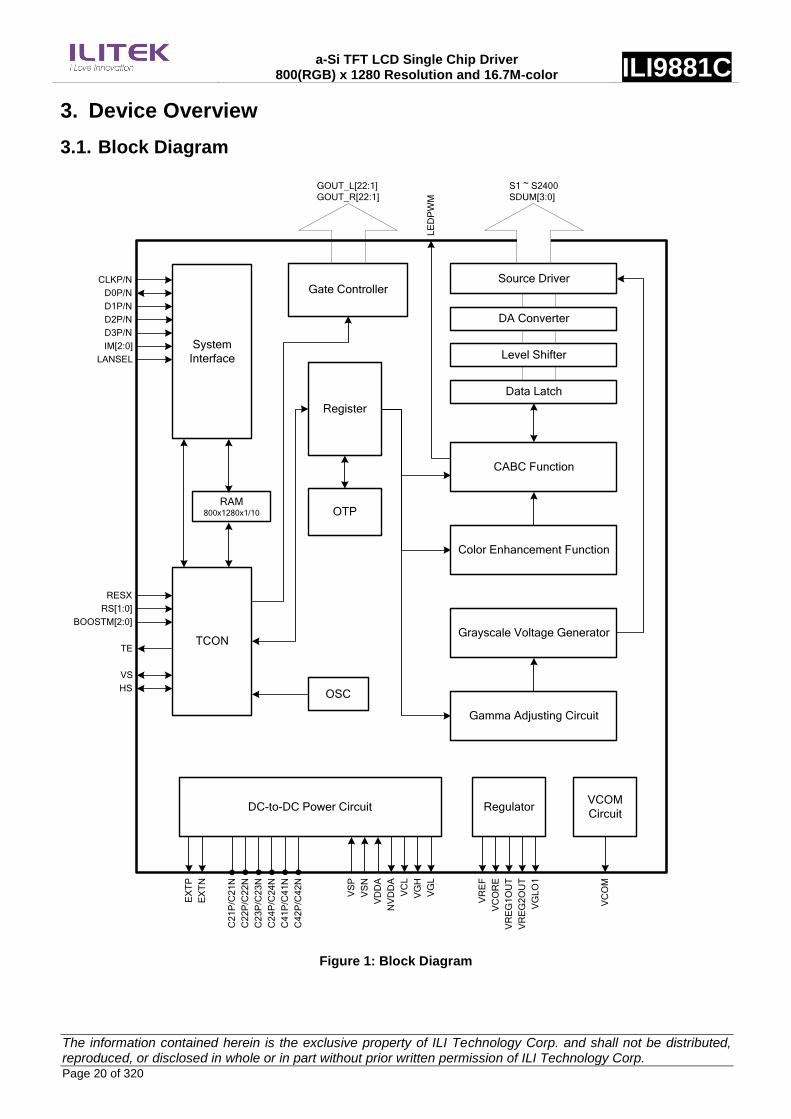
a-Si TFT LCD Single Chip Driver 800(RGB) x 1280 Resolution and 16.7M-color ILI9881C
The information contained herein is the exclusive property of ILI Technology Corp. and shall not be distributed, reproduced, or disclosed in whole or in part without prior written permission of ILI Technology Corp. Page 20 of 320
3. Device Overview
3.1. Block Diagram
IM[2:0]
DC-to-DC Power Circuit
S1 ~ S2400
SDUM[3:0]E
XT
P
System
Interface
CLKP/N
Register
DA Converter
Level Shifter
Data Latch
C2
2P
/C2
2N
C2
3P
/C2
3N
C2
4P
/C2
4N
C2
1P
/C2
1N
C4
1P
/C4
1N
D0P/N
OTP
LANSEL
D1P/N
D2P/N
D3P/N
TCONTE
RESX
RS[1:0]
BOOSTM[2:0]
Gate Controller
GOUT_L[22:1]
GOUT_R[22:1]
C4
2P
/C4
2N
EX
TN
VD
DA
NV
DD
A
VC
L
VG
H
VG
L
Regulator
VR
EF
VC
OR
E
Source Driver
VG
LO
1
VR
EG
1O
UT
VR
EG
2O
UT
OSC
VCOM
Circuit
VC
OM
CABC Function
Color Enhancement Function
Gamma Adjusting Circuit
Grayscale Voltage Generator
LE
DP
WM
VS
N
VS
P
VS
HS
RAM800x1280x1/10
Figure 1: Block Diagram

a-Si TFT LCD Single Chip Driver 800(RGB) x 1280 Resolution and 16.7M-color ILI9881C
The information contained herein is the exclusive property of ILI Technology Corp. and shall not be distributed, reproduced, or disclosed in whole or in part without prior written permission of ILI Technology Corp. Page 21 of 320
3.2. Block Function Description
3.2.1. System Interface
The ILI9881C supports DSI interfaces. The interface mode and the lane number of DSI interface can be selected
by hardware pins IM[2:0], LANSEL and control register MIPI_LANE_SEL (Page4_R00h).
3.2.2. Grayscale Voltage Generating Circuit
The grayscale voltage generating circuit generates a liquid crystal drive voltage that corresponds to the grayscale
level set in the Gamma correction register. The ILI9881C can display 16.7M colors at maximum.
3.2.3. TCON
The TCON generates timing signals for internal circuits. Timing for display operations are outputted separately so
that they do not interfere with each other.
3.2.4. OSC
The ILI9881C incorporates with an RC oscillator circuit. Command settings are used to change the frame
frequency.
3.2.5. RAM
The LCD driver incorporates the RAM (800x1280)/10 bits = 12800 bytes, which can store pattern data of a
800(RGB) x 1280 resolution with data compression in the Idle Mode.
3.2.6. Source Driver Circuit
The LCD display driver circuit consists of a 2404-output source driver (S1~S2400 and SDUM[3:0]). The display
pattern data is latched when 800RGB pixels of data are input. The voltage is output from the source driver
according to the latched data.
3.2.7. Gate Controller Circuit
The panel control circuit outputs GOUT_L/R[22:1] signals at either the VGH or VGL level.
3.2.8. DC-to-DC Power Supply Circuit
The LCD drive power supply circuit generates the voltage levels for driving a panel. Voltage levels are adjusted
according to the register setting.
3.2.9. CABC (Content Adaptive Brightness Control)
The CABC (Content Adaptive Brightness Control) dynamic backlight control function is used to reduce the power
consumption of the luminance source.

a-Si TFT LCD Single Chip Driver 800(RGB) x 1280 Resolution and 16.7M-color ILI9881C
The information contained herein is the exclusive property of ILI Technology Corp. and shall not be distributed, reproduced, or disclosed in whole or in part without prior written permission of ILI Technology Corp. Page 22 of 320
3.3. Pin Descriptions
Table 1: Pin Definition
Pin Name I/O Type Descriptions
Global Control Pins
IM[2:0] I VDDI
- Interface mode select pins. Notes: (1) IM[2:0] pins are used to configure lane sequence and polarity (2) The bottom table is an example for MIPI 4 lane setting
External Pad Set Configuration of MIPI Lane
IM2 IM1 IM0 D0P/N Pin D1P/N Pin CLKP/N Pin D2P/N Pin D3P/N Pin
0 0 0 D3P/N D2P/N CLKP/N D1P/N D0P/N
0 0 1 D3N/P D2N/P CLKN/P D1N/P D0N/P
0 1 0 D0P/N D1P/N CLKP/N D2P/N D3P/N
0 1 1 D0N/P D1N/P CLKN/P D2N/P D3N/P
1 0 0 D3P/N D0P/N CLKP/N D1P/N D2P/N
1 0 1 D3N/P D0N/P CLKN/P D1N/P D2N/P
1 1 0 D2P/N D1P/N CLKP/N D0P/N D3P/N
1 1 1 D2N/P D1N/P CLKN/P D0N/P D3N/P
RS[1:0] I VDDI
- Resolution selection pins. RS1 RS0 Resolution
0 0 800 (RGB) x (480 + (4 x NL)) gate line
0 1 768 (RGB) x (480 + (4 x NL)) gate line
1 0 720 (RGB) x (480 + (4 x NL)) gate line
1 1 640 (RGB) x (480 + (4 x NL)) gate line
LANSEL I VDDI
- MIPI DSI Lane number selection pin LANSEL=”1”, MIPI DSI is 2 Lane mode LANSEL=”0”, MIPI DSI is 3 or 4 Lane mode Note: Please reference “Table 2 DSI Interface Lane Mode Selection”
BOOSTM[2:0] I VDDI
- Power type selection pins Page4_R6Eh
DI_PWR_REG BOOSTM2 BOOSTM1 BOOSTM0 NOTE
0 0 0 1 Power Mode 2A External IOVCC, VSP and VSN (VCI=VSP)
Note 1
1 0 0 1 Power Mode 4 External IOVCC, VCI, VSP and VSN
X 0 1 0 Power Mode 3 External IOVCC and VCI (with ILI4003)
prohibited -
The default value of DI_PWR_REG is “1”. Note 1: VCI and VSP pads must be connected by external metal path.
RESX I VDDI
- The external reset input Initializes the chip with a low input. Be sure to execute a power-on reset after supplying power. Fix to VDDI level when not in use.
TE O VDDI - Tearing effect output pin. Leave the pin open when not in use.
VS I/O VDDI - Touch synchronization signal (VSOUT). Fix to VSS level when not in use.
HS I/O VDDI - Touch synchronization signal (HSOUT). Fix to VSS level when not in use.
LEDPWM O VDDI - LCD backlight control PWM output pin. Leave the pin open when not in use.
DSI Interface Signal Pins
CLKP CLKN
I LVDSVDD - MIPI DSI differential clock pair Leave it open or fix to LVDSVSS level when not in use.
D0P D0N
I/O LVDSVDD - MIPI DSI differential data pair. (Data lane 0) Leave it open or fix to LVDSVSS level when not in use.

a-Si TFT LCD Single Chip Driver 800(RGB) x 1280 Resolution and 16.7M-color ILI9881C
The information contained herein is the exclusive property of ILI Technology Corp. and shall not be distributed, reproduced, or disclosed in whole or in part without prior written permission of ILI Technology Corp. Page 23 of 320
D1P D1N
I LVDSVDD - MIPI DSI differential data pair. (Data lane 1) Leave it open or fix to LVDSVSS level when not in use.
D2P D2N
I LVDSVDD - MIPI DSI differential data pair. (Data lane 2) Leave it open or fix to LVDSVSS level when not in use.
D3P D3N
I LVDSVDD - MIPI DSI differential data pair. (Data lane 3) Leave it open or fix to LVDSVSS level when not in use.
Source / Panel Control / VCOM Signal Pins
S[2400:1] O Analog
- Output source driver signals. The D/A converted 256-gray-scale analog voltage output. Source output mapping with different resolution
Disaply resulation Source channels
800 (RGB) S1 ~ S2400
768 (RGB) S1 ~ S1152, S1249 ~ S2400
720 (RGB) S1 ~ S1080, S1321 ~ S2400
640 (RGB) S1 ~ S960, S1441 ~ S2400
800 (RGB) + Zig-Zag S1 ~ S2400, SDUM[2:1]
SDUM[3:0] O Analog - Dummy Source Leave the pin open when not in use.
GOUT_L[22:1] O Analog - Gate control signals for panel in left side of IC Leave the pin open when not in use.
GOUT_R[22:1] O Analog - Gate control signals for panel in right side of IC Leave the pin open when not in use.
VCOM O Analog - Regulator output for common voltage of panel Connect to a stabilizing capacitor between VCOM and VSSA.
Power Supply Pins
VCI I Power Supply
- Power supply for analog circuits. Connect to an external power supply of 2.5V to 6.0V
VCIREF I Power Supply
- Power supply for analog circuits. Connect to an external power supply of 2.5V to 6.0V
VDDI I Power Supply
- Power supply for I/O pads. Connect to an external power supply of 1.65V to 3.3V
VCC1 I Power Supply
- Power supply for internal logic regulator. Connect to an external power supply of 1.75V to 6.0V
VCC2 I Power Supply
- Power supply for internal logic regulator. Connect to an external power supply of 1.75V to 6.0V
VDDAM I Power Supply
- Power supply for MIPI DSI regulator. Connect to an external power supply of 1.75V to 3.3V
VSP I Power Supply
- Input voltage from step-up circuit. Connect to an external power supply of 4.5V to
6.0V
VSN I Power Supply
- Input voltage from step-up circuit. Connect to an external power supply of -4.5V to
-6.0V.
VSSA I Ground - System ground for the analog circuit In the case of COG, connect to GND on the FPC to prevent noise.
VSSREF I Ground - System ground for the analog circuit In the case of COG, connect to GND on the FPC to prevent noise.
LVDSVSS I Ground - System ground for MIPI DSI analog ground In the case of COG, connect to GND on the FPC to prevent noise.
VSS I Ground - System ground for digital circuit In the case of COG, connect to GND on the FPC to prevent noise.
MTP_PWR I Power Supply
- Input power for OTP programming. MTP_PWR=8. 5V When not under programming, let MTP_PWR float or connect to ground.
DC-to-DC Circuit Pins
VREG1OUT O Analog - Regulator output voltage from VSP, It‟s for positive gray scale voltage. Connect to a stabilizing capacitor between GVDD and VSSA.
VREG2OUT O Analog - Regulator output voltage from VSN, It‟s for negative gray scale voltage. Connect to a stabilizing capacitor between NGVDD and VSSA.
VCL O Analog - Output voltage from step-up circuit

a-Si TFT LCD Single Chip Driver 800(RGB) x 1280 Resolution and 16.7M-color ILI9881C
The information contained herein is the exclusive property of ILI Technology Corp. and shall not be distributed, reproduced, or disclosed in whole or in part without prior written permission of ILI Technology Corp. Page 24 of 320
Connect to a stabilizing capacitor between VCL and VSSA.
VGH O Analog - Output voltage from step-up circuit Connect to a stabilizing capacitor between VGH and VSSA.
VGL O Analog - Output voltage from step-up circuit Connect to a stabilizing capacitor between VGL and VSSA.
VGLO1 O Analog - Negative power supply to panel GIP circuits If need different VGL voltage, must connect to a stabilizing capacitor between VGLO1 and VSSA.
EXTP O VCI - Control signal output to generate VSP
EXTN O VCI - Control signal output to generate VSN
LVDSVDD O Analog - MIPI DSI regulator output Connect to a stabilizing capacitor between LVDSVDD and LVDSVSS.
VREF O Analog - Reference voltage from internal band gap circuit (1.8V typical) Connect to a stabilizing capacitor between VREF and VSSA.
VCORE O Analog - Internal logic regulator output (1.5V typical) Connect to a stabilizing capacitor between VCORE and VSSA.
C21P/ C21N C22P / C22N
I/O Step-up
Capacitor - Connect the charge-pumping capacitor for generating VGH level.
C23P / C23N C24P / C24N
I/O Step-up
Capacitor - Connect the charge-pumping capacitor for generating VGL level.
C41P / C41N C42P / C42N
I/O Step-up
Capacitor - Connect the charge-pumping capacitor for generating VCL level.
Test / Dummy Pins
PCLK I VDDI - Test pins Unused pins should be left open.
D[7:0] I/O VDDI - Test pins Unused pins should be left open or connected to VSS, VDDI.
TEST[5:0] I/O VDDI - Test pins Unused pins should be left open or connected to VSS, VDDI.
TOUT[3:0] I/O VDDI - Test pins Unused pins should be left open or connected to VSS, VDDI.
VTESTOUTP O Analog - Analog test output pin Let it open.
VTESTOUTN O Analog - Analog test output pin Let it open.
CSX I VDDI - Test pins Fix to VDDI or VSS level when not in use.
DCX I VDDI - Test pins Fix to VDDI or VSS level when not in use.
SCL I VDDI - Test pins Fix to VDDI or VSS level when not in use.
SDI I VDDI - Test pins Leave the pin open when not in use.
SDO O VDDI - Test pins Leave the pin open when not in use.
TE1 O VDDI - Test pins. Leave the pin open when not in use.
C31P - - - Dummy pins Let it open.
VCOMR - - - Dummy pins Let it open.
VGLO2DUMMY - - - Dummy pins Let it open.
DUMMYR1 - Analog - dummy pins Propose to connect these two pads separately when use for bonding resistance measurement
VSSDUMMY - - - Dummy pins Let it open.
a-Si TFT LCD Single Chip Driver 800(RGB) x 1280 Resolution and 16.7M-color ILI9881C
The information contained herein is the exclusive property of ILI Technology Corp. and shall not be distributed, reproduced, or disclosed in whole or in part without prior written permission of ILI Technology Corp. Page 25 of 320
DUMMY[85:3] - - - Dummy pins Let it open.
DUMMYN - - - Dummy pins Let it open.
DUMMYP - - - Dummy pins Let it open.

a-Si TFT LCD Single Chip Driver 800(RGB) x 1280 Resolution and 16.7M-color ILI9881C
The information contained herein is the exclusive property of ILI Technology Corp. and shall not be distributed, reproduced, or disclosed in whole or in part without prior written permission of ILI Technology Corp. Page 26 of 320
3.4. Pin Assignment Chip Size: 27840 um x 875 um
Pad Location: Pad Center.
Coordinate Origin: Chip center
Bump Size:
1. 30um x 73um
Pad 1 to 606.
2. 16um x 65um
Pad 607 to 3090.
Bump View
DUMMY1
GOUT_L1
GOUT_L2
GOUT_L3
GOUT_L4
GOUT_L5
GOUT_L6
GOUT_L7
GOUT_L8
GOUT_L9
GOUT_L10
GOUT_L11
GOUT_L12
GOUT_L13
GOUT_L14
GOUT_L15
GOUT_L16
GOUT_L17
GOUT_L18
GOUT_L19
GOUT_L20
GOUT_L21
GOUT_L22
VCOM
VCOM
VCOM
VSSA
VSSA
VSSA
VSSA
VSSA
VSSA
VSSA
VSSA
VSSA
VSSA
VTESTOUTP
VTESTOUTP
LVDSVSS
D0N
D0N
D0N
D0N
D0N
D0N
D0P
D0P
D0P
D0P
D0P
D0P
LVDSVSS
D1N
D1N
D1N
D1N
D1N
D1N
D1P
D1P
D1P
D1P
D1P
D1P
LVDSVSS
CLKN
CLKN
CLKN
CLKN
CLKN
CLKN
CLKP
CLKP
CLKP
CLKP
CLKP
CLKP
LVDSVSS
D2N
D2N
D2N
D2N
D2N
D2N
D2P
D2P
D2P
D2P
D2P
D2P
LVDSVSS
D3N
D3N
D3N
D3N
D3N
D3N
D3P
D3P
D3P
D3P
D3P
D3P
LVDSVSS
LVDSVSS
LVDSVSS
LVDSVSS
LVDSVSS
LVDSVSS
LVDSVSS
LVDSVSS
LVDSVSS
LVDSVSS
LVDSVSS
LVDSVSS
LVDSVDD
LVDSVDD
LVDSVDD
LVDSVDD
LVDSVDD
LVDSVDD
LVDSVDD
LVDSVDD
LVDSVDD
LVDSVDD
LVDSVDD
LVDSVDD
VDDAM
VDDAM
VDDAM
VDDAM
VDDAM
VDDAM
VDDAM
VDDAM
VDDAM
VDDAM
VDDAM
VDDAM
VCC1
VCC1
VCC1
VCC1
VCC1
VCC1
VCC1
VCC1
VCC1
VCC1
VCC1
VCC1
VCC1
VCC1
VCC1
VCORE
VCORE
VCORE
VCORE
VCORE
VCORE
VCORE
VCORE
VCORE
VCORE
VCORE
VCORE
VCORE
VCORE
VCORE
VSS
VSS
VSS
VSS
VSS
VSS
VSS
VSS
VSS
VSS
VSS
VSS
VSS
VSS
VSS
TOUT3
TOUT3
TOUT2
TOUT2
TOUT1
TOUT1
TOUT0
TOUT0
DUMMYP
DUMMYP
DUMMYP
DUMMYP
DUMMYP
DUMMYP
DUMMYP
DUMMYP
DUMMYP
DUMMYP
DUMMYP
DUMMYP
DUMMYP
DUMMYP
DUMMYP
DUMMYP
DUMMYP
DUMMYP
DUMMYP
DUMMYP
DUMMYP
DUMMYP
DUMMYP
DUMMYP
DUMMYP
DUMMYP
DUMMYP
DUMMYP
DUMMYP
DUMMYP
DUMMYP
DUMMYP
DUMMYP
DUMMYP
DUMMYP
DUMMYP
DUMMYP
DUMMYP
DUMMYP
DUMMYP
DUMMYP
DUMMYP
DUMMYP
DUMMYP
DUMMYP
VSS
VSS
D7
D7
D6
D6
D5
D5
D4
D4
D3
D3
D2
D2
D1
D1
D0
D0
HS
HS
VS
VS
VSSDUMMY
VSSDUMMY
PCLK
PCLK
DCX
DCX
CSX
CSX
SCL
SCL
SDI
SDI
SDO
SDO
LEDPWM
LEDPWM
LEDPWM
LEDPWM
TE
TE
TE
TE
TE
TE
TE1
TE1
TE1
TE1
TE1
TE1
RESX
RESX
RESX
RESX
TEST5
TEST4
TEST3
TEST2
TEST1
TEST0
VSSDUMMY
VSSDUMMY
IM0
IM0
VDDI
VDDI
IM1
IM1
IM2
IM2
RS0
RS0
VDDI
VDDI
RS1
RS1
VSS
VSS
LANSEL
LANSEL
VDDI
VDDI
BOOSTM0
BOOSTM0
BOOSTM2
BOOSTM2
BOOSTM1
BOOSTM1
VCC2
VCC2
VCC2
VCC2
VCC2
VCC2
VCC2
VCC2
VCC2
VCC2
VCORE
VCORE
VCORE
VCORE
VCORE
VCORE
VCORE
VCORE
VCORE
VCORE
VSS
VSS
VSS
VSS
VSS
VSS
VSS
VSS
VSS
VSS
EXTN
EXTN
EXTN
EXTN
EXTN
EXTN
EXTN
EXTN
EXTP
EXTP
EXTP
EXTP
EXTP
EXTP
EXTP
EXTP
MTP_PWR
MTP_PWR
MTP_PWR
MTP_PWR
MTP_PWR
MTP_PWR
DUMMYN
DUMMYN
VCIREF
VCIREF
VCIREF
VCIREF
VCIREF
VTESTOUTN
VTESTOUTN
DUMMYN
DUMMYN
DUMMYN
DUMMYN
DUMMYN
DUMMYN
VSSREF
VSSREF
VSSREF
VSSREF
VSSA
VSSA
VSSA
VSSA
VSSA
VSSA
VSSA
VREG1OUT
VREG1OUT
VREG1OUT
VREG2OUT
VREG2OUT
VREG2OUT
VREF
VREF
VREF
VSS
VSS
VSS
VSS
VSS
VCI
VCI
VCI
VCI
VCI
VCI
VCI
VCI
VCL
VCL
VCL
VCL
VCL
C41P
C41P
C41P
C41P
C41P
C41P
C41P
C41N
C41N
C41N
C41N
C41N
C41N
C41N
C42P
C42P
C42P
C42P
C42P
C42P
C42P
C42N
C42N
C42N
C42N
C42N
C42N
C42N
VSP
VSP
VSP
VSP
VSP
VSP
VSP
VSN
VSN
VSN
VSN
VSN
VSN
VSN
C21N
C21N
C21N
C21N
C21N
C21N
C21N
C21P
C21P
C21P
C21P
C21P
C21P
C21P
C22N
C22N
C22N
C22N
C22N
C22N
C22N
C22P
C22P
C22P
C22P
C22P
C22P
C22P
VGH
VGH
VGH
VGH
VGH
VGH
VCI
VCI
VCI
VCI
VCI
VCI
VSS
VSS
VSS
VSS
VSS
VSS
VSS
VSS
C23P
C23P
C23P
C23P
C23P
C23P
C23P
C23N
C23N
C23N
C23N
C23N
C23N
C23N
C24P
C24P
C24P
C24P
C24P
C24P
C24P
C24N
C24N
C24N
C24N
C24N
C24N
C24N
VGL
VGL
VGL
VGL
VGL
VGL
C31P
C31P
C31P
C31P
C31P
C31P
C31P
VGLO2DUMMY
VGLO2DUMMY
VGLO2DUMMY
VGLO2DUMMY
VGLO2DUMMY
VGLO2DUMMY
VGLO2DUMMY
VGLO1
VGLO1
VGLO1
VGLO1
VGLO1
VGLO1
VCOMR
VCOMR
DUMMYR1
DUMMYR1
VCOM
VCOM
VCOM
GOUT_R22
GOUT_R21
GOUT_R20
GOUT_R19
GOUT_R18
GOUT_R17
GOUT_R16
GOUT_R15
GOUT_R14
GOUT_R13
GOUT_R12
GOUT_R11
GOUT_R10
GOUT_R9
GOUT_R8
GOUT_R7
GOUT_R6
GOUT_R5
GOUT_R4
GOUT_R3
GOUT_R2
GOUT_R1
DUMMY2
DUMMY80DUMMY81
DUMMY82DUMMY3
DUMMY4DUMMY5
DUMMY6DUMMY7
DUMMY8DUMMY9
SDUM3SDUM2
S2400S2399
S2398S2397
S2396S2395
S2394S2393
S2392S2391
S2390S2389
S2388S2387
S2386S2385
S2384S2383
S2382S2381
S2380S2379
S2378S2377
S2376S2375
S2374S2373
S2372S2371
S2370S2369
S2368S2367
S2366S2365
S2364S2363
S2362S2361
S2360S2359
S2358S2357
S2356S2355
S2354S2353
S2352S2351
S2350S2349
S2348S2347
S2346S2345
S2344S2343
S2342S2341
S2340S2339
S2338S2337
S2336S2335
S2334S2333
S2332S2331
S2330S2329
S2328S2327
S2326S2325
S2324S2323
S2322S2321
S2320S2319
S2318S2317
S2316S2315
S2314S2313
S2312S2311
S2310S2309
S2308S2307
S2306S2305
S2304S2303
S2302S2301
S2300S2299
S2298S2297
S2296S2295
S2294S2293
S2292S2291
S2290S2289
S2288S2287
S2286S2285
S2284S2283
S2282S2281
S2280S2279
S2278S2277
S2276S2275
S2274S2273
S2272S2271
S2270S2269
S2268S2267
S2266S2265
S2264S2263
S2262S2261
S2260S2259
S2258S2257
S2256S2255
S2254S2253
S2252S2251
S2250S2249
S2248S2247
S2246S2245
S2244S2243
S2242S2241
S2240S2239
S2238S2237
S2236S2235
S2234S2233
S2232S2231
S2230S2229
S2228S2227
S2226S2225
S2224S2223
S2222S2221
S2220S2219
S2218S2217
S2216S2215
S2214S2213
S2212S2211
S2210S2209
S2208S2207
S2206S2205
S2204S2203
S2202S2201
S2200S2199
S2198S2197
S2196S2195
S2194S2193
S2192S2191
S2190S2189
S2188S2187
S2186S2185
S2184S2183
S2182S2181
S2180S2179
S2178S2177
S2176S2175
S2174S2173
S2172S2171
S2170S2169
S2168S2167
S2166S2165
S2164S2163
S2162S2161
S2160S2159
S2158S2157
S2156S2155
S2154S2153
S2152S2151
S2150S2149
S2148S2147
S2146S2145
S2144S2143
S2142S2141
S2140S2139
S2138S2137
S2136S2135
S2134S2133
S2132S2131
S2130S2129
S2128S2127
S2126S2125
S2124S2123
S2122S2121
S2120S2119
S2118S2117
S2116S2115
S2114S2113
S2112S2111
S2110S2109
S2108S2107
S2106S2105
S2104S2103
S2102S2101
S2100S2099
S2098S2097
S2096S2095
S2094S2093
S2092S2091
S2090S2089
S2088S2087
S2086S2085
S2084S2083
S2082S2081
S2080S2079
S2078S2077
S2076S2075
S2074S2073
S2072S2071
S2070S2069
S2068S2067
S2066S2065
S2064S2063
S2062S2061
S2060S2059
S2058S2057
S2056S2055
S2054S2053
S2052S2051
S2050S2049
S2048S2047
S2046S2045
S2044S2043
S2042S2041
S2040S2039
S2038S2037
S2036S2035
S2034S2033
S2032S2031
S2030S2029
S2028S2027
S2026S2025
S2024S2023
S2022S2021
S2020S2019S2018
S2017S2016
S2015S2014
S2013S2012
S2011S2010
S2009S2008
S2007S2006
S2005S2004S2003
S2002S2001
S2000S1999
S1998S1997
S1996S1995
S1994S1993
S1992S1991
S1990S1989
S1988S1987
S1986S1985
S1984S1983
S1982S1981
S1980S1979
S1978S1977
S1976S1975
S1974S1973
S1972S1971
S1970S1969
S1968S1967
S1966S1965
S1964S1963
S1962S1961
S1960S1959
S1958S1957
S1956S1955
S1954S1953
S1952S1951
S1950S1949
S1948S1947
S1946S1945
S1944S1943
S1942S1941
S1940S1939
S1938 S1937S1936
S1935S1934
S1933S1932
S1931S1930
S1929S1928
S1927S1926
S1925S1924
S1923S1922
S1921S1920
S1919S1918
S1917S1916
S1915S1914
S1913S1912
S1911S1910
S1909S1908
S1907S1906
S1905S1904
S1903S1902
S1901S1900
S1899 S1898S1897
S1896S1895
S1894S1893
S1892S1891
S1890S1889
S1888S1887
S1886S1885S1884
S1883S1882
S1881S1880
S1879S1878
S1877S1876
S1875S1874
S1873S1872
S1871S1870S1869
S1868S1867
S1866S1865
S1864S1863
S1862S1861
S1860S1859
S1858S1857
S1856S1855
S1854S1853
S1852S1851
S1850S1849
S1848S1847
S1846S1845
S1844S1843
S1842S1841
S1840S1839
S1838S1837
S1836S1835
S1834S1833
S1832S1831
S1830S1829
S1828S1827
S1826S1825
S1824S1823
S1822S1821
S1820S1819
S1818S1817 S1816
S1815S1814
S1813S1812
S1811S1810
S1809S1808
S1807S1806
S1805S1804
S1803S1802
S1801DUMMY11
DUMMY12DUMMY13
DUMMY14DUMMY15
DUMMY16DUMMY17
DUMMY18DUMMY19
DUMMY20DUMMY21
DUMMY22DUMMY23
DUMMY24DUMMY25
DUMMY26DUMMY27
DUMMY28S1800
S1799S1798
S1797S1796
S1795S1794
S1793S1792
S1791S1790
S1789S1788
S1787S1786
S1785S1784
S1783S1782 S1781
S1780S1779
S1778S1777
S1776S1775
S1774S1773
S1772S1771
S1770S1769
S1768S1767S1766
S1765S1764
S1763S1762
S1761S1760
S1759S1758 S1757
S1756S1755
S1754S1753S1752
S1751S1750
S1749S1748
S1747S1746
S1745S1744
S1743 S1742S1741
S1740S1739
S1738S1737
S1736S1735
S1734S1733
S1732S1731
S1730S1729
S1728S1727
S1726S1725
S1724S1723
S1722S1721
S1720S1719
S1718S1717
S1716S1715
S1714S1713S1712
S1711S1710
S1709S1708
S1707S1706
S1705S1704
S1703S1702
S1701S1700
S1699S1698
S1697S1696
S1695S1694
S1693S1692
S1691S1690
S1689S1688
S1687S1686
S1685S1684
S1683S1682
S1681S1680
S1679S1678
S1677S1676 S1675
S1674S1673
S1672S1671
S1670S1669
S1668S1667
S1666S1665
S1664S1663
S1662S1661
S1660S1659
S1658S1657
S1656S1655
S1654S1653
S1652S1651
S1650S1649
S1648S1647 S1646
S1645S1644
S1643S1642
S1641S1640
S1639S1638
S1637 S1636S1635
S1634S1633
S1632S1631
S1630S1629
S1628S1627
S1626S1625
S1624S1623
S1622 S1621S1620
S1619S1618
S1617S1616
S1615S1614
S1613S1612
S1611S1610
S1609S1608 S1607
S1606S1605
S1604S1603
S1602S1601
S1600S1599
S1598S1597
S1596S1595
S1594S1593S1592
S1591S1590
S1589S1588
S1587S1586
S1585S1584
S1583S1582
S1581S1580
S1579S1578
S1577S1576
S1575S1574
S1573S1572
S1571S1570
S1569S1568
S1567S1566
S1565S1564
S1563S1562
S1561S1560
S1559S1558
S1557S1556
S1555S1554S1553
S1552S1551
S1550S1549
S1548S1547
S1546S1545
S1544S1543
S1542S1541
S1540S1539
S1538S1537
S1536S1535
S1534S1533
S1532S1531
S1530S1529
S1528S1527
S1526S1525
S1524S1523
S1522S1521
S1520S1519
S1518S1517
S1516S1515
S1514S1513
S1512S1511
S1510S1509
S1508S1507
S1506S1505
S1504S1503
S1502S1501
S1500S1499
S1498S1497
S1496S1495
S1494S1493
S1492S1491
S1490S1489
S1488S1487 S1486
S1485S1484
S1483S1482
S1481S1480
S1479S1478
S1477S1476
S1475S1474
S1473 S1472S1471
S1470S1469
S1468S1467
S1466S1465
S1464S1463
S1462S1461
S1460S1459
S1458S1457
S1456S1455
S1454S1453
S1452S1451
S1450S1449 S1448
S1447S1446
S1445S1444S1443
S1442S1441
S1440S1439
S1438S1437
S1436S1435
S1434 S1433S1432
S1431S1430
S1429S1428
S1427S1426
S1425S1424
S1423S1422
S1421S1420
S1419S1418
S1417S1416
S1415S1414
S1413S1412
S1411S1410
S1409S1408
S1407S1406
S1405S1404
S1403S1402
S1401S1400
S1399S1398
S1397S1396
S1395S1394
S1393S1392
S1391S1390
S1389S1388
S1387S1386
S1385S1384
S1383S1382
S1381S1380
S1379S1378
S1377S1376
S1375S1374
S1373S1372
S1371S1370
S1369S1368
S1367 S1366S1365
S1364S1363
S1362S1361
S1360S1359
S1358S1357
S1356S1355
S1354S1353
S1352 S1351S1350
S1349S1348
S1347S1346
S1345S1344
S1343S1342
S1341S1340
S1339S1338
S1337S1336
S1335S1334
S1333S1332
S1331S1330
S1329S1328 S1327
S1326S1325
S1324S1323
S1322S1321
S1320S1319
S1318S1317
S1316S1315
S1314 S1313S1312
S1311S1310
S1309S1308
S1307S1306
S1305S1304
S1303S1302
S1301S1300
S1299 S1298S1297
S1296S1295
S1294S1293
S1292S1291
S1290S1289
S1288S1287
S1286S1285
S1284S1283
S1282S1281
S1280S1279
S1278S1277
S1276S1275 S1274
S1273S1272
S1271S1270
S1269S1268
S1267S1266
S1265S1264
S1263S1262
S1261S1260
S1259S1258
S1257S1256
S1255S1254
S1253S1252
S1251S1250
S1249S1248
S1247S1246S1245
S1244S1243
S1242S1241
S1240S1239
S1238S1237
S1236S1235
S1234S1233
S1232S1231
S1230S1229
S1228S1227
S1226S1225
S1224S1223
S1222S1221
S1220S1219
S1218S1217
S1216S1215
S1214S1213
S1212S1211
S1210S1209
S1208S1207
S1206S1205
S1204S1203
S1202S1201
DUMMY29DUMMY30
DUMMY31DUMMY32
DUMMY33DUMMY34
DUMMY35DUMMY36DUMMY37
DUMMY38DUMMY39
DUMMY40DUMMY41
DUMMY42DUMMY43
DUMMY44DUMMY45
DUMMY46DUMMY47
DUMMY48DUMMY49
DUMMY50DUMMY51DUMMY52
S1200S1199
S1198S1197
S1196S1195
S1194S1193
S1192S1191
S1190S1189
S1188 S1187S1186
S1185S1184
S1183S1182
S1181S1180
S1179S1178 S1177
S1176S1175
S1174S1173
S1172S1171
S1170S1169
S1168S1167
S1166S1165
S1164S1163
S1162S1161
S1160S1159
S1158S1157
S1156S1155
S1154S1153
S1152S1151
S1150S1149 S1148
S1147S1146
S1145S1144
S1143S1142
S1141S1140
S1139S1138
S1137S1136
S1135S1134
S1133S1132
S1131S1130
S1129S1128
S1127S1126
S1125S1124
S1123S1122
S1121S1120
S1119S1118
S1117S1116
S1115S1114
S1113S1112
S1111S1110
S1109S1108
S1107S1106
S1105S1104
S1103S1102
S1101S1100
S1099S1098
S1097S1096
S1095S1094
S1093S1092
S1091S1090
S1089S1088
S1087S1086
S1085S1084
S1083S1082
S1081S1080
S1079S1078
S1077S1076
S1075S1074
S1073S1072S1071
S1070S1069
S1068S1067 S1066
S1065S1064
S1063S1062
S1061S1060
S1059S1058
S1057S1056S1055
S1054S1053
S1052S1051
S1050S1049
S1048S1047
S1046S1045
S1044S1043 S1042
S1041S1040
S1039S1038
S1037S1036
S1035S1034
S1033S1032
S1031S1030
S1029 S1028S1027
S1026S1025
S1024S1023
S1022S1021
S1020S1019
S1018S1017
S1016S1015
S1014S1013
S1012S1011
S1010S1009
S1008S1007
S1006S1005
S1004S1003
S1002S1001
S1000S999
S998S997
S996S995
S994S993
S992S991
S990 S989S988
S987S986
S985S984
S983S982
S981S980
S979S978
S977S976
S975 S974S973
S972S971
S970S969
S968S967
S966S965
S964S963
S962S961
S960S959
S958S957
S956S955
S954S953
S952S951
S950S949
S948S947
S946S945
S944S943
S942S941
S940S939
S938S937
S936S935
S934S933
S932S931
S930S929
S928S927
S926S925
S924S923
S922S921
S920S919
S918S917
S916S915
S914S913
S912S911
S910S909
S908 S907S906
S905S904
S903S902
S901S900
S899S898
S897S896
S895S894
S893S892
S891S890
S889S888
S887S886
S885S884
S883S882
S881S880
S879 S878S877
S876S875
S874S873
S872S871
S870S869 S868
S867S866
S865S864
S863S862
S861S860
S859S858
S857S856
S855S854
S853S852
S851S850
S849S848
S847S846
S845S844
S843S842
S841S840
S839S838
S837S836
S835S834
S833S832
S831S830
S829S828
S827S826
S825S824
S823S822
S821S820
S819S818
S817S816
S815S814
S813S812
S811S810
S809S808
S807S806
S805S804
S803S802S801
S800S799
S798S797
S796S795
S794S793
S792S791
S790S789
S788S787S786
S785S784
S783S782
S781S780
S779S778
S777S776
S775S774
S773S772
S771S770
S769S768
S767S766
S765S764
S763S762S761
S760S759
S758 S757S756
S755S754
S753S752
S751S750
S749S748S747
S746S745
S744S743
S742S741
S740S739
S738S737
S736S735
S734 S733S732
S731S730
S729S728
S727S726
S725S724
S723S722
S721S720
S719S718
S717S716
S715S714
S713S712
S711S710 S709
S708S707
S706S705
S704S703
S702S701
S700S699
S698S697
S696S695
S694S693
S692S691
S690S689
S688S687
S686S685
S684S683
S682S681 S680
S679S678
S677S676
S675S674
S673S672
S671S670
S669S668
S667S666
S665S664
S663S662
S661S660
S659S658
S657S656
S655S654
S653S652
S651S650
S649S648
S647S646
S645S644
S643S642
S641S640
S639S638
S637S636
S635S634
S633S632
S631S630
S629S628
S627S626
S625S624
S623S622
S621S620
S619S618
S617S616
S615S614
S613S612S611
S610S609
S608S607
S606S605
S604S603
S602S601
DUMMY53DUMMY54DUMMY55
DUMMY56DUMMY57
DUMMY58DUMMY59
DUMMY60DUMMY61
DUMMY62DUMMY63
DUMMY64DUMMY65DUMMY66
DUMMY67DUMMY68
DUMMY69DUMMY70
S600S599
S598S597
S596S595
S594S593
S592S591
S590S589
S588S587
S586S585
S584S583
S582S581
S580S579
S578 S577S576
S575S574
S573S572
S571S570
S569S568
S567S566
S565S564
S563S562
S561S560
S559S558
S557S556
S555S554
S553S552
S551S550
S549S548
S547S546
S545S544
S543S542
S541S540
S539S538
S537S536
S535S534
S533S532
S531S530
S529S528
S527S526
S525S524
S523S522
S521S520
S519S518
S517S516
S515S514
S513S512
S511S510
S509S508
S507S506
S505S504
S503S502
S501S500
S499S498
S497S496S495
S494S493
S492S491
S490S489
S488S487
S486 S485S484
S483S482
S481S480
S479S478
S477S476
S475S474
S473S472S471
S470S469
S468S467
S466S465
S464S463
S462S461
S460S459
S458S457S456
S455S454
S453S452
S451S450
S449S448
S447S446
S445S444
S443 S442S441
S440S439
S438S437
S436S435
S434S433
S432S431
S430S429
S428S427
S426S425
S424S423
S422S421
S420S419 S418
S417S416
S415S414
S413S412
S411S410
S409S408
S407S406
S405S404 S403
S402S401
S400S399
S398S397
S396S395
S394S393
S392S391
S390S389
S388S387
S386S385
S384S383
S382S381
S380S379
S378S377
S376S375
S374S373
S372S371
S370S369
S368S367
S366S365
S364S363
S362S361
S360S359
S358S357
S356S355
S354S353
S352S351
S350S349
S348S347
S346S345
S344S343
S342S341
S340S339
S338S337S336
S335S334
S333S332
S331S330
S329S328
S327S326
S325S324
S323S322S321
S320S319
S318S317
S316S315
S314S313
S312S311
S310S309
S308 S307S306
S305S304
S303S302
S301S300
S299S298S297
S296S295
S294S293
S292S291
S290S289
S288S287
S286S285
S284S283
S282S281
S280S279
S278S277
S276S275
S274S273
S272S271
S270S269
S268S267
S266S265
S264S263
S262S261
S260S259
S258S257
S256S255
S254S253
S252S251
S250S249
S248S247
S246S245
S244S243
S242S241
S240S239
S238S237
S236S235
S234S233
S232S231
S230S229
S228S227
S226S225
S224S223
S222S221
S220S219
S218S217
S216 S215S214
S213S212
S211S210
S209S208
S207S206 S205
S204S203
S202S201
S200S199
S198S197
S196S195
S194S193
S192 S191S190
S189S188
S187S186
S185S184
S183S182
S181S180
S179S178
S177 S176S175
S174S173
S172S171
S170S169
S168S167
S166S165
S164S163S162
S161S160
S159S158
S157S156
S155S154
S153S152
S151S150
S149S148S147
S146S145
S144S143
S142S141
S140S139
S138S137
S136S135
S134S133
S132S131
S130S129
S128S127
S126S125
S124S123
S122S121
S120S119
S118S117
S116S115
S114S113
S112S111
S110 S109S108
S107S106
S105S104
S103S102
S101S100
S99S98
S97S96
S95 S94S93
S92S91
S90S89
S88S87
S86S85
S84S83
S82S81
S80S79
S78S77
S76S75
S74S73
S72S71
S70S69
S68S67
S66S65
S64S63
S62S61
S60S59
S58S57
S56S55
S54S53
S52S51
S50S49
S48S47
S46S45
S44S43
S42 S41S40
S39S38
S37S36
S35S34
S33S32
S31S30
S29S28S27
S26S25
S24S23
S22S21
S20S19
S18 S17S16
S15S14
S13S12S11
S10S9
S8S7
S6S5
S4S3
S2S1
SDUM1SDUM0
DUMMY73DUMMY74
DUMMY75DUMMY76
DUMMY77DUMMY78
DUMMY79DUMMY83
DUMMY84DUMMY85
-13000-12000
-11000-10000
-9000-8000
-7000-6000
-5000-4000
-3000-2000
-10001000
20003000
40005000
60007000
80009000
1000011000
1200013000
X
Y
(0,0)
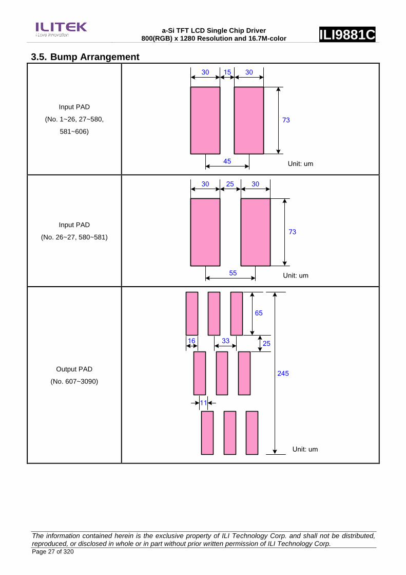
a-Si TFT LCD Single Chip Driver 800(RGB) x 1280 Resolution and 16.7M-color ILI9881C
The information contained herein is the exclusive property of ILI Technology Corp. and shall not be distributed, reproduced, or disclosed in whole or in part without prior written permission of ILI Technology Corp. Page 27 of 320
3.5. Bump Arrangement
Input PAD
(No. 1~26, 27~580,
581~606)
73
30 15 30
45 Unit: um
Input PAD
(No. 26~27, 580~581) 73
30 25 30
55 Unit: um
Output PAD
(No. 607~3090)
65
33
Unit: um
16 25
11
245
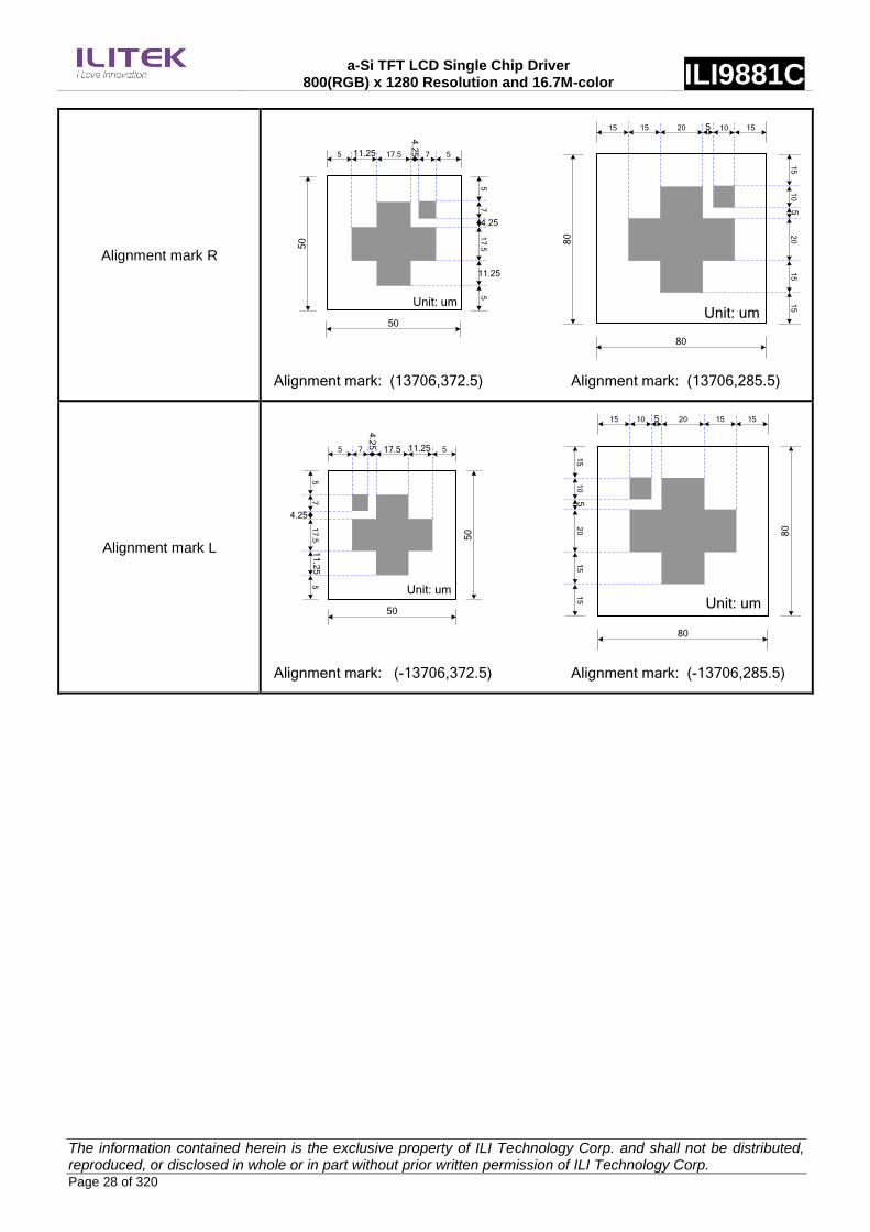
a-Si TFT LCD Single Chip Driver 800(RGB) x 1280 Resolution and 16.7M-color ILI9881C
The information contained herein is the exclusive property of ILI Technology Corp. and shall not be distributed, reproduced, or disclosed in whole or in part without prior written permission of ILI Technology Corp. Page 28 of 320
Alignment mark R
Alignment mark: (13706,372.5) Alignment mark: (13706,285.5)
20
15
15 20 10
Unit: um
10
5
51
51
5
1515
80
80
4.2
5
17
.5
17.5 7
Unit: um
75
5
55
50
50
4.25
11.25
11.25
Alignment mark L
Alignment mark: (-13706,372.5) Alignment mark: (-13706,285.5)
80
80
20
15
10 20 15
Unit: um
10
5
5
1515
15
15
4.2
5
50
50
17
.5
7
Unit: um
7
55
55
4.25
17.5
11
.25
11.25

a-Si TFT LCD Single Chip Driver 800(RGB) x 1280 Resolution and 16.7M-color ILI9881C
The information contained herein is the exclusive property of ILI Technology Corp. and shall not be distributed, reproduced, or disclosed in whole or in part without prior written permission of ILI Technology Corp. Page 29 of 320
3.6. Pad Coordination
No. Name X Y No. Name X Y No. Name X Y No. Name X Y
1 DUMMY1 -13622.5 -361 101 D3P -9112.5 -361 201 DUMMYP -4612.5 -361 301 VSSDUMMY -112.5 -361
2 GOUT_L1 -13577.5 -361 102 D3P -9067.5 -361 202 DUMMYP -4567.5 -361 302 IM0 -67.5 -361
3 GOUT_L2 -13532.5 -361 103 D3P -9022.5 -361 203 DUMMYP -4522.5 -361 303 IM0 -22.5 -361
4 GOUT_L3 -13487.5 -361 104 LVDSVSS -8977.5 -361 204 DUMMYP -4477.5 -361 304 VDDI 22.5 -361
5 GOUT_L4 -13442.5 -361 105 LVDSVSS -8932.5 -361 205 DUMMYP -4432.5 -361 305 VDDI 67.5 -361
6 GOUT_L5 -13397.5 -361 106 LVDSVSS -8887.5 -361 206 DUMMYP -4387.5 -361 306 IM1 112.5 -361
7 GOUT_L6 -13352.5 -361 107 LVDSVSS -8842.5 -361 207 DUMMYP -4342.5 -361 307 IM1 157.5 -361
8 GOUT_L7 -13307.5 -361 108 LVDSVSS -8797.5 -361 208 DUMMYP -4297.5 -361 308 IM2 202.5 -361
9 GOUT_L8 -13262.5 -361 109 LVDSVSS -8752.5 -361 209 DUMMYP -4252.5 -361 309 IM2 247.5 -361
10 GOUT_L9 -13217.5 -361 110 LVDSVSS -8707.5 -361 210 DUMMYP -4207.5 -361 310 RS0 292.5 -361
11 GOUT_L10 -13172.5 -361 111 LVDSVSS -8662.5 -361 211 DUMMYP -4162.5 -361 311 RS0 337.5 -361
12 GOUT_L11 -13127.5 -361 112 LVDSVSS -8617.5 -361 212 DUMMYP -4117.5 -361 312 VDDI 382.5 -361
13 GOUT_L12 -13082.5 -361 113 LVDSVSS -8572.5 -361 213 DUMMYP -4072.5 -361 313 VDDI 427.5 -361
14 GOUT_L13 -13037.5 -361 114 LVDSVSS -8527.5 -361 214 DUMMYP -4027.5 -361 314 RS1 472.5 -361
15 GOUT_L14 -12992.5 -361 115 LVDSVSS -8482.5 -361 215 DUMMYP -3982.5 -361 315 RS1 517.5 -361
16 GOUT_L15 -12947.5 -361 116 LVDSVDD -8437.5 -361 216 DUMMYP -3937.5 -361 316 VSS 562.5 -361
17 GOUT_L16 -12902.5 -361 117 LVDSVDD -8392.5 -361 217 DUMMYP -3892.5 -361 317 VSS 607.5 -361
18 GOUT_L17 -12857.5 -361 118 LVDSVDD -8347.5 -361 218 DUMMYP -3847.5 -361 318 LANSEL 652.5 -361
19 GOUT_L18 -12812.5 -361 119 LVDSVDD -8302.5 -361 219 DUMMYP -3802.5 -361 319 LANSEL 697.5 -361
20 GOUT_L19 -12767.5 -361 120 LVDSVDD -8257.5 -361 220 DUMMYP -3757.5 -361 320 VDDI 742.5 -361
21 GOUT_L20 -12722.5 -361 121 LVDSVDD -8212.5 -361 221 DUMMYP -3712.5 -361 321 VDDI 787.5 -361
22 GOUT_L21 -12677.5 -361 122 LVDSVDD -8167.5 -361 222 DUMMYP -3667.5 -361 322 BOOSTM0 832.5 -361
23 GOUT_L22 -12632.5 -361 123 LVDSVDD -8122.5 -361 223 DUMMYP -3622.5 -361 323 BOOSTM0 877.5 -361
24 VCOM -12587.5 -361 124 LVDSVDD -8077.5 -361 224 DUMMYP -3577.5 -361 324 BOOSTM2 922.5 -361
25 VCOM -12542.5 -361 125 LVDSVDD -8032.5 -361 225 DUMMYP -3532.5 -361 325 BOOSTM2 967.5 -361
26 VCOM -12497.5 -361 126 LVDSVDD -7987.5 -361 226 DUMMYP -3487.5 -361 326 BOOSTM1 1012.5 -361
27 VSSA -12442.5 -361 127 LVDSVDD -7942.5 -361 227 DUMMYP -3442.5 -361 327 BOOSTM1 1057.5 -361
28 VSSA -12397.5 -361 128 VDDAM -7897.5 -361 228 DUMMYP -3397.5 -361 328 VCC2 1102.5 -361
29 VSSA -12352.5 -361 129 VDDAM -7852.5 -361 229 DUMMYP -3352.5 -361 329 VCC2 1147.5 -361
30 VSSA -12307.5 -361 130 VDDAM -7807.5 -361 230 DUMMYP -3307.5 -361 330 VCC2 1192.5 -361
31 VSSA -12262.5 -361 131 VDDAM -7762.5 -361 231 DUMMYP -3262.5 -361 331 VCC2 1237.5 -361
32 VSSA -12217.5 -361 132 VDDAM -7717.5 -361 232 DUMMYP -3217.5 -361 332 VCC2 1282.5 -361
33 VSSA -12172.5 -361 133 VDDAM -7672.5 -361 233 DUMMYP -3172.5 -361 333 VCC2 1327.5 -361
34 VSSA -12127.5 -361 134 VDDAM -7627.5 -361 234 DUMMYP -3127.5 -361 334 VCC2 1372.5 -361
35 VSSA -12082.5 -361 135 VDDAM -7582.5 -361 235 DUMMYP -3082.5 -361 335 VCC2 1417.5 -361
36 VSSA -12037.5 -361 136 VDDAM -7537.5 -361 236 DUMMYP -3037.5 -361 336 VCC2 1462.5 -361
37 VTESTOUTP -11992.5 -361 137 VDDAM -7492.5 -361 237 DUMMYP -2992.5 -361 337 VCC2 1507.5 -361
38 VTESTOUTP -11947.5 -361 138 VDDAM -7447.5 -361 238 VSS -2947.5 -361 338 VCORE 1552.5 -361
39 LVDSVSS -11902.5 -361 139 VDDAM -7402.5 -361 239 VSS -2902.5 -361 339 VCORE 1597.5 -361
40 D0N -11857.5 -361 140 VCC1 -7357.5 -361 240 D7 -2857.5 -361 340 VCORE 1642.5 -361
41 D0N -11812.5 -361 141 VCC1 -7312.5 -361 241 D7 -2812.5 -361 341 VCORE 1687.5 -361
42 D0N -11767.5 -361 142 VCC1 -7267.5 -361 242 D6 -2767.5 -361 342 VCORE 1732.5 -361
43 D0N -11722.5 -361 143 VCC1 -7222.5 -361 243 D6 -2722.5 -361 343 VCORE 1777.5 -361
44 D0N -11677.5 -361 144 VCC1 -7177.5 -361 244 D5 -2677.5 -361 344 VCORE 1822.5 -361
45 D0N -11632.5 -361 145 VCC1 -7132.5 -361 245 D5 -2632.5 -361 345 VCORE 1867.5 -361
46 D0P -11587.5 -361 146 VCC1 -7087.5 -361 246 D4 -2587.5 -361 346 VCORE 1912.5 -361
47 D0P -11542.5 -361 147 VCC1 -7042.5 -361 247 D4 -2542.5 -361 347 VCORE 1957.5 -361
48 D0P -11497.5 -361 148 VCC1 -6997.5 -361 248 D3 -2497.5 -361 348 VSS 2002.5 -361
49 D0P -11452.5 -361 149 VCC1 -6952.5 -361 249 D3 -2452.5 -361 349 VSS 2047.5 -361
50 D0P -11407.5 -361 150 VCC1 -6907.5 -361 250 D2 -2407.5 -361 350 VSS 2092.5 -361
51 D0P -11362.5 -361 151 VCC1 -6862.5 -361 251 D2 -2362.5 -361 351 VSS 2137.5 -361
52 LVDSVSS -11317.5 -361 152 VCC1 -6817.5 -361 252 D1 -2317.5 -361 352 VSS 2182.5 -361
53 D1N -11272.5 -361 153 VCC1 -6772.5 -361 253 D1 -2272.5 -361 353 VSS 2227.5 -361
54 D1N -11227.5 -361 154 VCC1 -6727.5 -361 254 D0 -2227.5 -361 354 VSS 2272.5 -361
55 D1N -11182.5 -361 155 VCORE -6682.5 -361 255 D0 -2182.5 -361 355 VSS 2317.5 -361
56 D1N -11137.5 -361 156 VCORE -6637.5 -361 256 HS -2137.5 -361 356 VSS 2362.5 -361
57 D1N -11092.5 -361 157 VCORE -6592.5 -361 257 HS -2092.5 -361 357 VSS 2407.5 -361
58 D1N -11047.5 -361 158 VCORE -6547.5 -361 258 VS -2047.5 -361 358 EXTN 2452.5 -361
59 D1P -11002.5 -361 159 VCORE -6502.5 -361 259 VS -2002.5 -361 359 EXTN 2497.5 -361
60 D1P -10957.5 -361 160 VCORE -6457.5 -361 260 VSSDUMMY -1957.5 -361 360 EXTN 2542.5 -361
61 D1P -10912.5 -361 161 VCORE -6412.5 -361 261 VSSDUMMY -1912.5 -361 361 EXTN 2587.5 -361
62 D1P -10867.5 -361 162 VCORE -6367.5 -361 262 PCLK -1867.5 -361 362 EXTN 2632.5 -361
63 D1P -10822.5 -361 163 VCORE -6322.5 -361 263 PCLK -1822.5 -361 363 EXTN 2677.5 -361
64 D1P -10777.5 -361 164 VCORE -6277.5 -361 264 DCX -1777.5 -361 364 EXTN 2722.5 -361
65 LVDSVSS -10732.5 -361 165 VCORE -6232.5 -361 265 DCX -1732.5 -361 365 EXTN 2767.5 -361
66 CLKN -10687.5 -361 166 VCORE -6187.5 -361 266 CSX -1687.5 -361 366 EXTP 2812.5 -361
67 CLKN -10642.5 -361 167 VCORE -6142.5 -361 267 CSX -1642.5 -361 367 EXTP 2857.5 -361
68 CLKN -10597.5 -361 168 VCORE -6097.5 -361 268 SCL -1597.5 -361 368 EXTP 2902.5 -361
69 CLKN -10552.5 -361 169 VCORE -6052.5 -361 269 SCL -1552.5 -361 369 EXTP 2947.5 -361
70 CLKN -10507.5 -361 170 VSS -6007.5 -361 270 SDI -1507.5 -361 370 EXTP 2992.5 -361
71 CLKN -10462.5 -361 171 VSS -5962.5 -361 271 SDI -1462.5 -361 371 EXTP 3037.5 -361
72 CLKP -10417.5 -361 172 VSS -5917.5 -361 272 SDO -1417.5 -361 372 EXTP 3082.5 -361
73 CLKP -10372.5 -361 173 VSS -5872.5 -361 273 SDO -1372.5 -361 373 EXTP 3127.5 -361
74 CLKP -10327.5 -361 174 VSS -5827.5 -361 274 LEDPWM -1327.5 -361 374 MTP_PWR 3172.5 -361
75 CLKP -10282.5 -361 175 VSS -5782.5 -361 275 LEDPWM -1282.5 -361 375 MTP_PWR 3217.5 -361
76 CLKP -10237.5 -361 176 VSS -5737.5 -361 276 LEDPWM -1237.5 -361 376 MTP_PWR 3262.5 -361
77 CLKP -10192.5 -361 177 VSS -5692.5 -361 277 LEDPWM -1192.5 -361 377 MTP_PWR 3307.5 -361
78 LVDSVSS -10147.5 -361 178 VSS -5647.5 -361 278 TE -1147.5 -361 378 MTP_PWR 3352.5 -361
79 D2N -10102.5 -361 179 VSS -5602.5 -361 279 TE -1102.5 -361 379 MTP_PWR 3397.5 -361
80 D2N -10057.5 -361 180 VSS -5557.5 -361 280 TE -1057.5 -361 380 DUMMYN 3442.5 -361
81 D2N -10012.5 -361 181 VSS -5512.5 -361 281 TE -1012.5 -361 381 DUMMYN 3487.5 -361
82 D2N -9967.5 -361 182 VSS -5467.5 -361 282 TE -967.5 -361 382 VCIREF 3532.5 -361
83 D2N -9922.5 -361 183 VSS -5422.5 -361 283 TE -922.5 -361 383 VCIREF 3577.5 -361
84 D2N -9877.5 -361 184 VSS -5377.5 -361 284 TE1 -877.5 -361 384 VCIREF 3622.5 -361
85 D2P -9832.5 -361 185 TOUT3 -5332.5 -361 285 TE1 -832.5 -361 385 VCIREF 3667.5 -361
86 D2P -9787.5 -361 186 TOUT3 -5287.5 -361 286 TE1 -787.5 -361 386 VCIREF 3712.5 -361
87 D2P -9742.5 -361 187 TOUT2 -5242.5 -361 287 TE1 -742.5 -361 387 VTESTOUTN 3757.5 -361
88 D2P -9697.5 -361 188 TOUT2 -5197.5 -361 288 TE1 -697.5 -361 388 VTESTOUTN 3802.5 -361
89 D2P -9652.5 -361 189 TOUT1 -5152.5 -361 289 TE1 -652.5 -361 389 DUMMYN 3847.5 -361
90 D2P -9607.5 -361 190 TOUT1 -5107.5 -361 290 RESX -607.5 -361 390 DUMMYN 3892.5 -361
91 LVDSVSS -9562.5 -361 191 TOUT0 -5062.5 -361 291 RESX -562.5 -361 391 DUMMYN 3937.5 -361
92 D3N -9517.5 -361 192 TOUT0 -5017.5 -361 292 RESX -517.5 -361 392 DUMMYN 3982.5 -361
93 D3N -9472.5 -361 193 DUMMYP -4972.5 -361 293 RESX -472.5 -361 393 DUMMYN 4027.5 -361
94 D3N -9427.5 -361 194 DUMMYP -4927.5 -361 294 TEST5 -427.5 -361 394 DUMMYN 4072.5 -361
95 D3N -9382.5 -361 195 DUMMYP -4882.5 -361 295 TEST4 -382.5 -361 395 VSSREF 4117.5 -361
96 D3N -9337.5 -361 196 DUMMYP -4837.5 -361 296 TEST3 -337.5 -361 396 VSSREF 4162.5 -361
97 D3N -9292.5 -361 197 DUMMYP -4792.5 -361 297 TEST2 -292.5 -361 397 VSSREF 4207.5 -361
98 D3P -9247.5 -361 198 DUMMYP -4747.5 -361 298 TEST1 -247.5 -361 398 VSSREF 4252.5 -361
99 D3P -9202.5 -361 199 DUMMYP -4702.5 -361 299 TEST0 -202.5 -361 399 VSSA 4297.5 -361
100 D3P -9157.5 -361 200 DUMMYP -4657.5 -361 300 VSSDUMMY -157.5 -361 400 VSSA 4342.5 -361
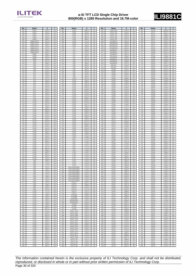
a-Si TFT LCD Single Chip Driver 800(RGB) x 1280 Resolution and 16.7M-color ILI9881C
The information contained herein is the exclusive property of ILI Technology Corp. and shall not be distributed, reproduced, or disclosed in whole or in part without prior written permission of ILI Technology Corp. Page 30 of 320
No. Name X Y No. Name X Y No. Name X Y No. Name X Y
401 VSSA 4387.5 -361 501 C22P 8887.5 -361 601 GOUT_R5 13397.5 -361 701 S2318 12622.5 275
402 VSSA 4432.5 -361 502 C22P 8932.5 -361 602 GOUT_R4 13442.5 -361 702 S2317 12611.5 365
403 VSSA 4477.5 -361 503 VGH 8977.5 -361 603 GOUT_R3 13487.5 -361 703 S2316 12600.5 185
404 VSSA 4522.5 -361 504 VGH 9022.5 -361 604 GOUT_R2 13532.5 -361 704 S2315 12589.5 275
405 VSSA 4567.5 -361 505 VGH 9067.5 -361 605 GOUT_R1 13577.5 -361 705 S2314 12578.5 365
406 VREG1OUT 4612.5 -361 506 VGH 9112.5 -361 606 DUMMY2 13622.5 -361 706 S2313 12567.5 185
407 VREG1OUT 4657.5 -361 507 VGH 9157.5 -361 607 DUMMY80 13656.5 185 707 S2312 12556.5 275
408 VREG1OUT 4702.5 -361 508 VGH 9202.5 -361 608 DUMMY81 13645.5 275 708 S2311 12545.5 365
409 VREG2OUT 4747.5 -361 509 VCI 9247.5 -361 609 DUMMY82 13634.5 365 709 S2310 12534.5 185
410 VREG2OUT 4792.5 -361 510 VCI 9292.5 -361 610 DUMMY3 13623.5 185 710 S2309 12523.5 275
411 VREG2OUT 4837.5 -361 511 VCI 9337.5 -361 611 DUMMY4 13612.5 275 711 S2308 12512.5 365
412 VREF 4882.5 -361 512 VCI 9382.5 -361 612 DUMMY5 13601.5 365 712 S2307 12501.5 185
413 VREF 4927.5 -361 513 VCI 9427.5 -361 613 DUMMY6 13590.5 185 713 S2306 12490.5 275
414 VREF 4972.5 -361 514 VCI 9472.5 -361 614 DUMMY7 13579.5 275 714 S2305 12479.5 365
415 VSS 5017.5 -361 515 VSS 9517.5 -361 615 DUMMY8 13568.5 365 715 S2304 12468.5 185
416 VSS 5062.5 -361 516 VSS 9562.5 -361 616 DUMMY9 13557.5 185 716 S2303 12457.5 275
417 VSS 5107.5 -361 517 VSS 9607.5 -361 617 SDUM3 13546.5 275 717 S2302 12446.5 365
418 VSS 5152.5 -361 518 VSS 9652.5 -361 618 SDUM2 13535.5 365 718 S2301 12435.5 185
419 VSS 5197.5 -361 519 VSS 9697.5 -361 619 S2400 13524.5 185 719 S2300 12424.5 275
420 VCI 5242.5 -361 520 VSS 9742.5 -361 620 S2399 13513.5 275 720 S2299 12413.5 365
421 VCI 5287.5 -361 521 VSS 9787.5 -361 621 S2398 13502.5 365 721 S2298 12402.5 185
422 VCI 5332.5 -361 522 VSS 9832.5 -361 622 S2397 13491.5 185 722 S2297 12391.5 275
423 VCI 5377.5 -361 523 C23P 9877.5 -361 623 S2396 13480.5 275 723 S2296 12380.5 365
424 VCI 5422.5 -361 524 C23P 9922.5 -361 624 S2395 13469.5 365 724 S2295 12369.5 185
425 VCI 5467.5 -361 525 C23P 9967.5 -361 625 S2394 13458.5 185 725 S2294 12358.5 275
426 VCI 5512.5 -361 526 C23P 10012.5 -361 626 S2393 13447.5 275 726 S2293 12347.5 365
427 VCI 5557.5 -361 527 C23P 10057.5 -361 627 S2392 13436.5 365 727 S2292 12336.5 185
428 VCL 5602.5 -361 528 C23P 10102.5 -361 628 S2391 13425.5 185 728 S2291 12325.5 275
429 VCL 5647.5 -361 529 C23P 10147.5 -361 629 S2390 13414.5 275 729 S2290 12314.5 365
430 VCL 5692.5 -361 530 C23N 10192.5 -361 630 S2389 13403.5 365 730 S2289 12303.5 185
431 VCL 5737.5 -361 531 C23N 10237.5 -361 631 S2388 13392.5 185 731 S2288 12292.5 275
432 VCL 5782.5 -361 532 C23N 10282.5 -361 632 S2387 13381.5 275 732 S2287 12281.5 365
433 C41P 5827.5 -361 533 C23N 10327.5 -361 633 S2386 13370.5 365 733 S2286 12270.5 185
434 C41P 5872.5 -361 534 C23N 10372.5 -361 634 S2385 13359.5 185 734 S2285 12259.5 275
435 C41P 5917.5 -361 535 C23N 10417.5 -361 635 S2384 13348.5 275 735 S2284 12248.5 365
436 C41P 5962.5 -361 536 C23N 10462.5 -361 636 S2383 13337.5 365 736 S2283 12237.5 185
437 C41P 6007.5 -361 537 C24P 10507.5 -361 637 S2382 13326.5 185 737 S2282 12226.5 275
438 C41P 6052.5 -361 538 C24P 10552.5 -361 638 S2381 13315.5 275 738 S2281 12215.5 365
439 C41P 6097.5 -361 539 C24P 10597.5 -361 639 S2380 13304.5 365 739 S2280 12204.5 185
440 C41N 6142.5 -361 540 C24P 10642.5 -361 640 S2379 13293.5 185 740 S2279 12193.5 275
441 C41N 6187.5 -361 541 C24P 10687.5 -361 641 S2378 13282.5 275 741 S2278 12182.5 365
442 C41N 6232.5 -361 542 C24P 10732.5 -361 642 S2377 13271.5 365 742 S2277 12171.5 185
443 C41N 6277.5 -361 543 C24P 10777.5 -361 643 S2376 13260.5 185 743 S2276 12160.5 275
444 C41N 6322.5 -361 544 C24N 10822.5 -361 644 S2375 13249.5 275 744 S2275 12149.5 365
445 C41N 6367.5 -361 545 C24N 10867.5 -361 645 S2374 13238.5 365 745 S2274 12138.5 185
446 C41N 6412.5 -361 546 C24N 10912.5 -361 646 S2373 13227.5 185 746 S2273 12127.5 275
447 C42P 6457.5 -361 547 C24N 10957.5 -361 647 S2372 13216.5 275 747 S2272 12116.5 365
448 C42P 6502.5 -361 548 C24N 11002.5 -361 648 S2371 13205.5 365 748 S2271 12105.5 185
449 C42P 6547.5 -361 549 C24N 11047.5 -361 649 S2370 13194.5 185 749 S2270 12094.5 275
450 C42P 6592.5 -361 550 C24N 11092.5 -361 650 S2369 13183.5 275 750 S2269 12083.5 365
451 C42P 6637.5 -361 551 VGL 11137.5 -361 651 S2368 13172.5 365 751 S2268 12072.5 185
452 C42P 6682.5 -361 552 VGL 11182.5 -361 652 S2367 13161.5 185 752 S2267 12061.5 275
453 C42P 6727.5 -361 553 VGL 11227.5 -361 653 S2366 13150.5 275 753 S2266 12050.5 365
454 C42N 6772.5 -361 554 VGL 11272.5 -361 654 S2365 13139.5 365 754 S2265 12039.5 185
455 C42N 6817.5 -361 555 VGL 11317.5 -361 655 S2364 13128.5 185 755 S2264 12028.5 275
456 C42N 6862.5 -361 556 VGL 11362.5 -361 656 S2363 13117.5 275 756 S2263 12017.5 365
457 C42N 6907.5 -361 557 C31P 11407.5 -361 657 S2362 13106.5 365 757 S2262 12006.5 185
458 C42N 6952.5 -361 558 C31P 11452.5 -361 658 S2361 13095.5 185 758 S2261 11995.5 275
459 C42N 6997.5 -361 559 C31P 11497.5 -361 659 S2360 13084.5 275 759 S2260 11984.5 365
460 C42N 7042.5 -361 560 C31P 11542.5 -361 660 S2359 13073.5 365 760 S2259 11973.5 185
461 VSP 7087.5 -361 561 C31P 11587.5 -361 661 S2358 13062.5 185 761 S2258 11962.5 275
462 VSP 7132.5 -361 562 C31P 11632.5 -361 662 S2357 13051.5 275 762 S2257 11951.5 365
463 VSP 7177.5 -361 563 C31P 11677.5 -361 663 S2356 13040.5 365 763 S2256 11940.5 185
464 VSP 7222.5 -361 564 VGLO2DUMMY 11722.5 -361 664 S2355 13029.5 185 764 S2255 11929.5 275
465 VSP 7267.5 -361 565 VGLO2DUMMY 11767.5 -361 665 S2354 13018.5 275 765 S2254 11918.5 365
466 VSP 7312.5 -361 566 VGLO2DUMMY 11812.5 -361 666 S2353 13007.5 365 766 S2253 11907.5 185
467 VSP 7357.5 -361 567 VGLO2DUMMY 11857.5 -361 667 S2352 12996.5 185 767 S2252 11896.5 275
468 VSN 7402.5 -361 568 VGLO2DUMMY 11902.5 -361 668 S2351 12985.5 275 768 S2251 11885.5 365
469 VSN 7447.5 -361 569 VGLO2DUMMY 11947.5 -361 669 S2350 12974.5 365 769 S2250 11874.5 185
470 VSN 7492.5 -361 570 VGLO2DUMMY 11992.5 -361 670 S2349 12963.5 185 770 S2249 11863.5 275
471 VSN 7537.5 -361 571 VGLO1 12037.5 -361 671 S2348 12952.5 275 771 S2248 11852.5 365
472 VSN 7582.5 -361 572 VGLO1 12082.5 -361 672 S2347 12941.5 365 772 S2247 11841.5 185
473 VSN 7627.5 -361 573 VGLO1 12127.5 -361 673 S2346 12930.5 185 773 S2246 11830.5 275
474 VSN 7672.5 -361 574 VGLO1 12172.5 -361 674 S2345 12919.5 275 774 S2245 11819.5 365
475 C21N 7717.5 -361 575 VGLO1 12217.5 -361 675 S2344 12908.5 365 775 S2244 11808.5 185
476 C21N 7762.5 -361 576 VGLO1 12262.5 -361 676 S2343 12897.5 185 776 S2243 11797.5 275
477 C21N 7807.5 -361 577 VCOMR 12307.5 -361 677 S2342 12886.5 275 777 S2242 11786.5 365
478 C21N 7852.5 -361 578 VCOMR 12352.5 -361 678 S2341 12875.5 365 778 S2241 11775.5 185
479 C21N 7897.5 -361 579 DUMMYR1 12397.5 -361 679 S2340 12864.5 185 779 S2240 11764.5 275
480 C21N 7942.5 -361 580 DUMMYR1 12442.5 -361 680 S2339 12853.5 275 780 S2239 11753.5 365
481 C21N 7987.5 -361 581 VCOM 12497.5 -361 681 S2338 12842.5 365 781 S2238 11742.5 185
482 C21P 8032.5 -361 582 VCOM 12542.5 -361 682 S2337 12831.5 185 782 S2237 11731.5 275
483 C21P 8077.5 -361 583 VCOM 12587.5 -361 683 S2336 12820.5 275 783 S2236 11720.5 365
484 C21P 8122.5 -361 584 GOUT_R22 12632.5 -361 684 S2335 12809.5 365 784 S2235 11709.5 185
485 C21P 8167.5 -361 585 GOUT_R21 12677.5 -361 685 S2334 12798.5 185 785 S2234 11698.5 275
486 C21P 8212.5 -361 586 GOUT_R20 12722.5 -361 686 S2333 12787.5 275 786 S2233 11687.5 365
487 C21P 8257.5 -361 587 GOUT_R19 12767.5 -361 687 S2332 12776.5 365 787 S2232 11676.5 185
488 C21P 8302.5 -361 588 GOUT_R18 12812.5 -361 688 S2331 12765.5 185 788 S2231 11665.5 275
489 C22N 8347.5 -361 589 GOUT_R17 12857.5 -361 689 S2330 12754.5 275 789 S2230 11654.5 365
490 C22N 8392.5 -361 590 GOUT_R16 12902.5 -361 690 S2329 12743.5 365 790 S2229 11643.5 185
491 C22N 8437.5 -361 591 GOUT_R15 12947.5 -361 691 S2328 12732.5 185 791 S2228 11632.5 275
492 C22N 8482.5 -361 592 GOUT_R14 12992.5 -361 692 S2327 12721.5 275 792 S2227 11621.5 365
493 C22N 8527.5 -361 593 GOUT_R13 13037.5 -361 693 S2326 12710.5 365 793 S2226 11610.5 185
494 C22N 8572.5 -361 594 GOUT_R12 13082.5 -361 694 S2325 12699.5 185 794 S2225 11599.5 275
495 C22N 8617.5 -361 595 GOUT_R11 13127.5 -361 695 S2324 12688.5 275 795 S2224 11588.5 365
496 C22P 8662.5 -361 596 GOUT_R10 13172.5 -361 696 S2323 12677.5 365 796 S2223 11577.5 185
497 C22P 8707.5 -361 597 GOUT_R9 13217.5 -361 697 S2322 12666.5 185 797 S2222 11566.5 275
498 C22P 8752.5 -361 598 GOUT_R8 13262.5 -361 698 S2321 12655.5 275 798 S2221 11555.5 365
499 C22P 8797.5 -361 599 GOUT_R7 13307.5 -361 699 S2320 12644.5 365 799 S2220 11544.5 185
500 C22P 8842.5 -361 600 GOUT_R6 13352.5 -361 700 S2319 12633.5 185 800 S2219 11533.5 275

a-Si TFT LCD Single Chip Driver 800(RGB) x 1280 Resolution and 16.7M-color ILI9881C
The information contained herein is the exclusive property of ILI Technology Corp. and shall not be distributed, reproduced, or disclosed in whole or in part without prior written permission of ILI Technology Corp. Page 31 of 320
No. Name X Y No. Name X Y No. Name X Y No. Name X Y
801 S2218 11522.5 365 901 S2118 10422.5 185 1001 S2018 9322.5 275 1101 S1918 8222.5 365
802 S2217 11511.5 185 902 S2117 10411.5 275 1002 S2017 9311.5 365 1102 S1917 8211.5 185
803 S2216 11500.5 275 903 S2116 10400.5 365 1003 S2016 9300.5 185 1103 S1916 8200.5 275
804 S2215 11489.5 365 904 S2115 10389.5 185 1004 S2015 9289.5 275 1104 S1915 8189.5 365
805 S2214 11478.5 185 905 S2114 10378.5 275 1005 S2014 9278.5 365 1105 S1914 8178.5 185
806 S2213 11467.5 275 906 S2113 10367.5 365 1006 S2013 9267.5 185 1106 S1913 8167.5 275
807 S2212 11456.5 365 907 S2112 10356.5 185 1007 S2012 9256.5 275 1107 S1912 8156.5 365
808 S2211 11445.5 185 908 S2111 10345.5 275 1008 S2011 9245.5 365 1108 S1911 8145.5 185
809 S2210 11434.5 275 909 S2110 10334.5 365 1009 S2010 9234.5 185 1109 S1910 8134.5 275
810 S2209 11423.5 365 910 S2109 10323.5 185 1010 S2009 9223.5 275 1110 S1909 8123.5 365
811 S2208 11412.5 185 911 S2108 10312.5 275 1011 S2008 9212.5 365 1111 S1908 8112.5 185
812 S2207 11401.5 275 912 S2107 10301.5 365 1012 S2007 9201.5 185 1112 S1907 8101.5 275
813 S2206 11390.5 365 913 S2106 10290.5 185 1013 S2006 9190.5 275 1113 S1906 8090.5 365
814 S2205 11379.5 185 914 S2105 10279.5 275 1014 S2005 9179.5 365 1114 S1905 8079.5 185
815 S2204 11368.5 275 915 S2104 10268.5 365 1015 S2004 9168.5 185 1115 S1904 8068.5 275
816 S2203 11357.5 365 916 S2103 10257.5 185 1016 S2003 9157.5 275 1116 S1903 8057.5 365
817 S2202 11346.5 185 917 S2102 10246.5 275 1017 S2002 9146.5 365 1117 S1902 8046.5 185
818 S2201 11335.5 275 918 S2101 10235.5 365 1018 S2001 9135.5 185 1118 S1901 8035.5 275
819 S2200 11324.5 365 919 S2100 10224.5 185 1019 S2000 9124.5 275 1119 S1900 8024.5 365
820 S2199 11313.5 185 920 S2099 10213.5 275 1020 S1999 9113.5 365 1120 S1899 8013.5 185
821 S2198 11302.5 275 921 S2098 10202.5 365 1021 S1998 9102.5 185 1121 S1898 8002.5 275
822 S2197 11291.5 365 922 S2097 10191.5 185 1022 S1997 9091.5 275 1122 S1897 7991.5 365
823 S2196 11280.5 185 923 S2096 10180.5 275 1023 S1996 9080.5 365 1123 S1896 7980.5 185
824 S2195 11269.5 275 924 S2095 10169.5 365 1024 S1995 9069.5 185 1124 S1895 7969.5 275
825 S2194 11258.5 365 925 S2094 10158.5 185 1025 S1994 9058.5 275 1125 S1894 7958.5 365
826 S2193 11247.5 185 926 S2093 10147.5 275 1026 S1993 9047.5 365 1126 S1893 7947.5 185
827 S2192 11236.5 275 927 S2092 10136.5 365 1027 S1992 9036.5 185 1127 S1892 7936.5 275
828 S2191 11225.5 365 928 S2091 10125.5 185 1028 S1991 9025.5 275 1128 S1891 7925.5 365
829 S2190 11214.5 185 929 S2090 10114.5 275 1029 S1990 9014.5 365 1129 S1890 7914.5 185
830 S2189 11203.5 275 930 S2089 10103.5 365 1030 S1989 9003.5 185 1130 S1889 7903.5 275
831 S2188 11192.5 365 931 S2088 10092.5 185 1031 S1988 8992.5 275 1131 S1888 7892.5 365
832 S2187 11181.5 185 932 S2087 10081.5 275 1032 S1987 8981.5 365 1132 S1887 7881.5 185
833 S2186 11170.5 275 933 S2086 10070.5 365 1033 S1986 8970.5 185 1133 S1886 7870.5 275
834 S2185 11159.5 365 934 S2085 10059.5 185 1034 S1985 8959.5 275 1134 S1885 7859.5 365
835 S2184 11148.5 185 935 S2084 10048.5 275 1035 S1984 8948.5 365 1135 S1884 7848.5 185
836 S2183 11137.5 275 936 S2083 10037.5 365 1036 S1983 8937.5 185 1136 S1883 7837.5 275
837 S2182 11126.5 365 937 S2082 10026.5 185 1037 S1982 8926.5 275 1137 S1882 7826.5 365
838 S2181 11115.5 185 938 S2081 10015.5 275 1038 S1981 8915.5 365 1138 S1881 7815.5 185
839 S2180 11104.5 275 939 S2080 10004.5 365 1039 S1980 8904.5 185 1139 S1880 7804.5 275
840 S2179 11093.5 365 940 S2079 9993.5 185 1040 S1979 8893.5 275 1140 S1879 7793.5 365
841 S2178 11082.5 185 941 S2078 9982.5 275 1041 S1978 8882.5 365 1141 S1878 7782.5 185
842 S2177 11071.5 275 942 S2077 9971.5 365 1042 S1977 8871.5 185 1142 S1877 7771.5 275
843 S2176 11060.5 365 943 S2076 9960.5 185 1043 S1976 8860.5 275 1143 S1876 7760.5 365
844 S2175 11049.5 185 944 S2075 9949.5 275 1044 S1975 8849.5 365 1144 S1875 7749.5 185
845 S2174 11038.5 275 945 S2074 9938.5 365 1045 S1974 8838.5 185 1145 S1874 7738.5 275
846 S2173 11027.5 365 946 S2073 9927.5 185 1046 S1973 8827.5 275 1146 S1873 7727.5 365
847 S2172 11016.5 185 947 S2072 9916.5 275 1047 S1972 8816.5 365 1147 S1872 7716.5 185
848 S2171 11005.5 275 948 S2071 9905.5 365 1048 S1971 8805.5 185 1148 S1871 7705.5 275
849 S2170 10994.5 365 949 S2070 9894.5 185 1049 S1970 8794.5 275 1149 S1870 7694.5 365
850 S2169 10983.5 185 950 S2069 9883.5 275 1050 S1969 8783.5 365 1150 S1869 7683.5 185
851 S2168 10972.5 275 951 S2068 9872.5 365 1051 S1968 8772.5 185 1151 S1868 7672.5 275
852 S2167 10961.5 365 952 S2067 9861.5 185 1052 S1967 8761.5 275 1152 S1867 7661.5 365
853 S2166 10950.5 185 953 S2066 9850.5 275 1053 S1966 8750.5 365 1153 S1866 7650.5 185
854 S2165 10939.5 275 954 S2065 9839.5 365 1054 S1965 8739.5 185 1154 S1865 7639.5 275
855 S2164 10928.5 365 955 S2064 9828.5 185 1055 S1964 8728.5 275 1155 S1864 7628.5 365
856 S2163 10917.5 185 956 S2063 9817.5 275 1056 S1963 8717.5 365 1156 S1863 7617.5 185
857 S2162 10906.5 275 957 S2062 9806.5 365 1057 S1962 8706.5 185 1157 S1862 7606.5 275
858 S2161 10895.5 365 958 S2061 9795.5 185 1058 S1961 8695.5 275 1158 S1861 7595.5 365
859 S2160 10884.5 185 959 S2060 9784.5 275 1059 S1960 8684.5 365 1159 S1860 7584.5 185
860 S2159 10873.5 275 960 S2059 9773.5 365 1060 S1959 8673.5 185 1160 S1859 7573.5 275
861 S2158 10862.5 365 961 S2058 9762.5 185 1061 S1958 8662.5 275 1161 S1858 7562.5 365
862 S2157 10851.5 185 962 S2057 9751.5 275 1062 S1957 8651.5 365 1162 S1857 7551.5 185
863 S2156 10840.5 275 963 S2056 9740.5 365 1063 S1956 8640.5 185 1163 S1856 7540.5 275
864 S2155 10829.5 365 964 S2055 9729.5 185 1064 S1955 8629.5 275 1164 S1855 7529.5 365
865 S2154 10818.5 185 965 S2054 9718.5 275 1065 S1954 8618.5 365 1165 S1854 7518.5 185
866 S2153 10807.5 275 966 S2053 9707.5 365 1066 S1953 8607.5 185 1166 S1853 7507.5 275
867 S2152 10796.5 365 967 S2052 9696.5 185 1067 S1952 8596.5 275 1167 S1852 7496.5 365
868 S2151 10785.5 185 968 S2051 9685.5 275 1068 S1951 8585.5 365 1168 S1851 7485.5 185
869 S2150 10774.5 275 969 S2050 9674.5 365 1069 S1950 8574.5 185 1169 S1850 7474.5 275
870 S2149 10763.5 365 970 S2049 9663.5 185 1070 S1949 8563.5 275 1170 S1849 7463.5 365
871 S2148 10752.5 185 971 S2048 9652.5 275 1071 S1948 8552.5 365 1171 S1848 7452.5 185
872 S2147 10741.5 275 972 S2047 9641.5 365 1072 S1947 8541.5 185 1172 S1847 7441.5 275
873 S2146 10730.5 365 973 S2046 9630.5 185 1073 S1946 8530.5 275 1173 S1846 7430.5 365
874 S2145 10719.5 185 974 S2045 9619.5 275 1074 S1945 8519.5 365 1174 S1845 7419.5 185
875 S2144 10708.5 275 975 S2044 9608.5 365 1075 S1944 8508.5 185 1175 S1844 7408.5 275
876 S2143 10697.5 365 976 S2043 9597.5 185 1076 S1943 8497.5 275 1176 S1843 7397.5 365
877 S2142 10686.5 185 977 S2042 9586.5 275 1077 S1942 8486.5 365 1177 S1842 7386.5 185
878 S2141 10675.5 275 978 S2041 9575.5 365 1078 S1941 8475.5 185 1178 S1841 7375.5 275
879 S2140 10664.5 365 979 S2040 9564.5 185 1079 S1940 8464.5 275 1179 S1840 7364.5 365
880 S2139 10653.5 185 980 S2039 9553.5 275 1080 S1939 8453.5 365 1180 S1839 7353.5 185
881 S2138 10642.5 275 981 S2038 9542.5 365 1081 S1938 8442.5 185 1181 S1838 7342.5 275
882 S2137 10631.5 365 982 S2037 9531.5 185 1082 S1937 8431.5 275 1182 S1837 7331.5 365
883 S2136 10620.5 185 983 S2036 9520.5 275 1083 S1936 8420.5 365 1183 S1836 7320.5 185
884 S2135 10609.5 275 984 S2035 9509.5 365 1084 S1935 8409.5 185 1184 S1835 7309.5 275
885 S2134 10598.5 365 985 S2034 9498.5 185 1085 S1934 8398.5 275 1185 S1834 7298.5 365
886 S2133 10587.5 185 986 S2033 9487.5 275 1086 S1933 8387.5 365 1186 S1833 7287.5 185
887 S2132 10576.5 275 987 S2032 9476.5 365 1087 S1932 8376.5 185 1187 S1832 7276.5 275
888 S2131 10565.5 365 988 S2031 9465.5 185 1088 S1931 8365.5 275 1188 S1831 7265.5 365
889 S2130 10554.5 185 989 S2030 9454.5 275 1089 S1930 8354.5 365 1189 S1830 7254.5 185
890 S2129 10543.5 275 990 S2029 9443.5 365 1090 S1929 8343.5 185 1190 S1829 7243.5 275
891 S2128 10532.5 365 991 S2028 9432.5 185 1091 S1928 8332.5 275 1191 S1828 7232.5 365
892 S2127 10521.5 185 992 S2027 9421.5 275 1092 S1927 8321.5 365 1192 S1827 7221.5 185
893 S2126 10510.5 275 993 S2026 9410.5 365 1093 S1926 8310.5 185 1193 S1826 7210.5 275
894 S2125 10499.5 365 994 S2025 9399.5 185 1094 S1925 8299.5 275 1194 S1825 7199.5 365
895 S2124 10488.5 185 995 S2024 9388.5 275 1095 S1924 8288.5 365 1195 S1824 7188.5 185
896 S2123 10477.5 275 996 S2023 9377.5 365 1096 S1923 8277.5 185 1196 S1823 7177.5 275
897 S2122 10466.5 365 997 S2022 9366.5 185 1097 S1922 8266.5 275 1197 S1822 7166.5 365
898 S2121 10455.5 185 998 S2021 9355.5 275 1098 S1921 8255.5 365 1198 S1821 7155.5 185
899 S2120 10444.5 275 999 S2020 9344.5 365 1099 S1920 8244.5 185 1199 S1820 7144.5 275
900 S2119 10433.5 365 1000 S2019 9333.5 185 1100 S1919 8233.5 275 1200 S1819 7133.5 365

a-Si TFT LCD Single Chip Driver 800(RGB) x 1280 Resolution and 16.7M-color ILI9881C
The information contained herein is the exclusive property of ILI Technology Corp. and shall not be distributed, reproduced, or disclosed in whole or in part without prior written permission of ILI Technology Corp. Page 32 of 320
No. Name X Y No. Name X Y No. Name X Y No. Name X Y
1201 S1818 7122.5 185 1301 S1736 6022.5 275 1401 S1636 4922.5 365 1501 S1536 3822.5 185
1202 S1817 7111.5 275 1302 S1735 6011.5 365 1402 S1635 4911.5 185 1502 S1535 3811.5 275
1203 S1816 7100.5 365 1303 S1734 6000.5 185 1403 S1634 4900.5 275 1503 S1534 3800.5 365
1204 S1815 7089.5 185 1304 S1733 5989.5 275 1404 S1633 4889.5 365 1504 S1533 3789.5 185
1205 S1814 7078.5 275 1305 S1732 5978.5 365 1405 S1632 4878.5 185 1505 S1532 3778.5 275
1206 S1813 7067.5 365 1306 S1731 5967.5 185 1406 S1631 4867.5 275 1506 S1531 3767.5 365
1207 S1812 7056.5 185 1307 S1730 5956.5 275 1407 S1630 4856.5 365 1507 S1530 3756.5 185
1208 S1811 7045.5 275 1308 S1729 5945.5 365 1408 S1629 4845.5 185 1508 S1529 3745.5 275
1209 S1810 7034.5 365 1309 S1728 5934.5 185 1409 S1628 4834.5 275 1509 S1528 3734.5 365
1210 S1809 7023.5 185 1310 S1727 5923.5 275 1410 S1627 4823.5 365 1510 S1527 3723.5 185
1211 S1808 7012.5 275 1311 S1726 5912.5 365 1411 S1626 4812.5 185 1511 S1526 3712.5 275
1212 S1807 7001.5 365 1312 S1725 5901.5 185 1412 S1625 4801.5 275 1512 S1525 3701.5 365
1213 S1806 6990.5 185 1313 S1724 5890.5 275 1413 S1624 4790.5 365 1513 S1524 3690.5 185
1214 S1805 6979.5 275 1314 S1723 5879.5 365 1414 S1623 4779.5 185 1514 S1523 3679.5 275
1215 S1804 6968.5 365 1315 S1722 5868.5 185 1415 S1622 4768.5 275 1515 S1522 3668.5 365
1216 S1803 6957.5 185 1316 S1721 5857.5 275 1416 S1621 4757.5 365 1516 S1521 3657.5 185
1217 S1802 6946.5 275 1317 S1720 5846.5 365 1417 S1620 4746.5 185 1517 S1520 3646.5 275
1218 S1801 6935.5 365 1318 S1719 5835.5 185 1418 S1619 4735.5 275 1518 S1519 3635.5 365
1219 DUMMY11 6924.5 185 1319 S1718 5824.5 275 1419 S1618 4724.5 365 1519 S1518 3624.5 185
1220 DUMMY12 6913.5 275 1320 S1717 5813.5 365 1420 S1617 4713.5 185 1520 S1517 3613.5 275
1221 DUMMY13 6902.5 365 1321 S1716 5802.5 185 1421 S1616 4702.5 275 1521 S1516 3602.5 365
1222 DUMMY14 6891.5 185 1322 S1715 5791.5 275 1422 S1615 4691.5 365 1522 S1515 3591.5 185
1223 DUMMY15 6880.5 275 1323 S1714 5780.5 365 1423 S1614 4680.5 185 1523 S1514 3580.5 275
1224 DUMMY16 6869.5 365 1324 S1713 5769.5 185 1424 S1613 4669.5 275 1524 S1513 3569.5 365
1225 DUMMY17 6858.5 185 1325 S1712 5758.5 275 1425 S1612 4658.5 365 1525 S1512 3558.5 185
1226 DUMMY18 6847.5 275 1326 S1711 5747.5 365 1426 S1611 4647.5 185 1526 S1511 3547.5 275
1227 DUMMY19 6836.5 365 1327 S1710 5736.5 185 1427 S1610 4636.5 275 1527 S1510 3536.5 365
1228 DUMMY20 6825.5 185 1328 S1709 5725.5 275 1428 S1609 4625.5 365 1528 S1509 3525.5 185
1229 DUMMY21 6814.5 275 1329 S1708 5714.5 365 1429 S1608 4614.5 185 1529 S1508 3514.5 275
1230 DUMMY22 6803.5 365 1330 S1707 5703.5 185 1430 S1607 4603.5 275 1530 S1507 3503.5 365
1231 DUMMY23 6792.5 185 1331 S1706 5692.5 275 1431 S1606 4592.5 365 1531 S1506 3492.5 185
1232 DUMMY24 6781.5 275 1332 S1705 5681.5 365 1432 S1605 4581.5 185 1532 S1505 3481.5 275
1233 DUMMY25 6770.5 365 1333 S1704 5670.5 185 1433 S1604 4570.5 275 1533 S1504 3470.5 365
1234 DUMMY26 6759.5 185 1334 S1703 5659.5 275 1434 S1603 4559.5 365 1534 S1503 3459.5 185
1235 DUMMY27 6748.5 275 1335 S1702 5648.5 365 1435 S1602 4548.5 185 1535 S1502 3448.5 275
1236 DUMMY28 6737.5 365 1336 S1701 5637.5 185 1436 S1601 4537.5 275 1536 S1501 3437.5 365
1237 S1800 6726.5 185 1337 S1700 5626.5 275 1437 S1600 4526.5 365 1537 S1500 3426.5 185
1238 S1799 6715.5 275 1338 S1699 5615.5 365 1438 S1599 4515.5 185 1538 S1499 3415.5 275
1239 S1798 6704.5 365 1339 S1698 5604.5 185 1439 S1598 4504.5 275 1539 S1498 3404.5 365
1240 S1797 6693.5 185 1340 S1697 5593.5 275 1440 S1597 4493.5 365 1540 S1497 3393.5 185
1241 S1796 6682.5 275 1341 S1696 5582.5 365 1441 S1596 4482.5 185 1541 S1496 3382.5 275
1242 S1795 6671.5 365 1342 S1695 5571.5 185 1442 S1595 4471.5 275 1542 S1495 3371.5 365
1243 S1794 6660.5 185 1343 S1694 5560.5 275 1443 S1594 4460.5 365 1543 S1494 3360.5 185
1244 S1793 6649.5 275 1344 S1693 5549.5 365 1444 S1593 4449.5 185 1544 S1493 3349.5 275
1245 S1792 6638.5 365 1345 S1692 5538.5 185 1445 S1592 4438.5 275 1545 S1492 3338.5 365
1246 S1791 6627.5 185 1346 S1691 5527.5 275 1446 S1591 4427.5 365 1546 S1491 3327.5 185
1247 S1790 6616.5 275 1347 S1690 5516.5 365 1447 S1590 4416.5 185 1547 S1490 3316.5 275
1248 S1789 6605.5 365 1348 S1689 5505.5 185 1448 S1589 4405.5 275 1548 S1489 3305.5 365
1249 S1788 6594.5 185 1349 S1688 5494.5 275 1449 S1588 4394.5 365 1549 S1488 3294.5 185
1250 S1787 6583.5 275 1350 S1687 5483.5 365 1450 S1587 4383.5 185 1550 S1487 3283.5 275
1251 S1786 6572.5 365 1351 S1686 5472.5 185 1451 S1586 4372.5 275 1551 S1486 3272.5 365
1252 S1785 6561.5 185 1352 S1685 5461.5 275 1452 S1585 4361.5 365 1552 S1485 3261.5 185
1253 S1784 6550.5 275 1353 S1684 5450.5 365 1453 S1584 4350.5 185 1553 S1484 3250.5 275
1254 S1783 6539.5 365 1354 S1683 5439.5 185 1454 S1583 4339.5 275 1554 S1483 3239.5 365
1255 S1782 6528.5 185 1355 S1682 5428.5 275 1455 S1582 4328.5 365 1555 S1482 3228.5 185
1256 S1781 6517.5 275 1356 S1681 5417.5 365 1456 S1581 4317.5 185 1556 S1481 3217.5 275
1257 S1780 6506.5 365 1357 S1680 5406.5 185 1457 S1580 4306.5 275 1557 S1480 3206.5 365
1258 S1779 6495.5 185 1358 S1679 5395.5 275 1458 S1579 4295.5 365 1558 S1479 3195.5 185
1259 S1778 6484.5 275 1359 S1678 5384.5 365 1459 S1578 4284.5 185 1559 S1478 3184.5 275
1260 S1777 6473.5 365 1360 S1677 5373.5 185 1460 S1577 4273.5 275 1560 S1477 3173.5 365
1261 S1776 6462.5 185 1361 S1676 5362.5 275 1461 S1576 4262.5 365 1561 S1476 3162.5 185
1262 S1775 6451.5 275 1362 S1675 5351.5 365 1462 S1575 4251.5 185 1562 S1475 3151.5 275
1263 S1774 6440.5 365 1363 S1674 5340.5 185 1463 S1574 4240.5 275 1563 S1474 3140.5 365
1264 S1773 6429.5 185 1364 S1673 5329.5 275 1464 S1573 4229.5 365 1564 S1473 3129.5 185
1265 S1772 6418.5 275 1365 S1672 5318.5 365 1465 S1572 4218.5 185 1565 S1472 3118.5 275
1266 S1771 6407.5 365 1366 S1671 5307.5 185 1466 S1571 4207.5 275 1566 S1471 3107.5 365
1267 S1770 6396.5 185 1367 S1670 5296.5 275 1467 S1570 4196.5 365 1567 S1470 3096.5 185
1268 S1769 6385.5 275 1368 S1669 5285.5 365 1468 S1569 4185.5 185 1568 S1469 3085.5 275
1269 S1768 6374.5 365 1369 S1668 5274.5 185 1469 S1568 4174.5 275 1569 S1468 3074.5 365
1270 S1767 6363.5 185 1370 S1667 5263.5 275 1470 S1567 4163.5 365 1570 S1467 3063.5 185
1271 S1766 6352.5 275 1371 S1666 5252.5 365 1471 S1566 4152.5 185 1571 S1466 3052.5 275
1272 S1765 6341.5 365 1372 S1665 5241.5 185 1472 S1565 4141.5 275 1572 S1465 3041.5 365
1273 S1764 6330.5 185 1373 S1664 5230.5 275 1473 S1564 4130.5 365 1573 S1464 3030.5 185
1274 S1763 6319.5 275 1374 S1663 5219.5 365 1474 S1563 4119.5 185 1574 S1463 3019.5 275
1275 S1762 6308.5 365 1375 S1662 5208.5 185 1475 S1562 4108.5 275 1575 S1462 3008.5 365
1276 S1761 6297.5 185 1376 S1661 5197.5 275 1476 S1561 4097.5 365 1576 S1461 2997.5 185
1277 S1760 6286.5 275 1377 S1660 5186.5 365 1477 S1560 4086.5 185 1577 S1460 2986.5 275
1278 S1759 6275.5 365 1378 S1659 5175.5 185 1478 S1559 4075.5 275 1578 S1459 2975.5 365
1279 S1758 6264.5 185 1379 S1658 5164.5 275 1479 S1558 4064.5 365 1579 S1458 2964.5 185
1280 S1757 6253.5 275 1380 S1657 5153.5 365 1480 S1557 4053.5 185 1580 S1457 2953.5 275
1281 S1756 6242.5 365 1381 S1656 5142.5 185 1481 S1556 4042.5 275 1581 S1456 2942.5 365
1282 S1755 6231.5 185 1382 S1655 5131.5 275 1482 S1555 4031.5 365 1582 S1455 2931.5 185
1283 S1754 6220.5 275 1383 S1654 5120.5 365 1483 S1554 4020.5 185 1583 S1454 2920.5 275
1284 S1753 6209.5 365 1384 S1653 5109.5 185 1484 S1553 4009.5 275 1584 S1453 2909.5 365
1285 S1752 6198.5 185 1385 S1652 5098.5 275 1485 S1552 3998.5 365 1585 S1452 2898.5 185
1286 S1751 6187.5 275 1386 S1651 5087.5 365 1486 S1551 3987.5 185 1586 S1451 2887.5 275
1287 S1750 6176.5 365 1387 S1650 5076.5 185 1487 S1550 3976.5 275 1587 S1450 2876.5 365
1288 S1749 6165.5 185 1388 S1649 5065.5 275 1488 S1549 3965.5 365 1588 S1449 2865.5 185
1289 S1748 6154.5 275 1389 S1648 5054.5 365 1489 S1548 3954.5 185 1589 S1448 2854.5 275
1290 S1747 6143.5 365 1390 S1647 5043.5 185 1490 S1547 3943.5 275 1590 S1447 2843.5 365
1291 S1746 6132.5 185 1391 S1646 5032.5 275 1491 S1546 3932.5 365 1591 S1446 2832.5 185
1292 S1745 6121.5 275 1392 S1645 5021.5 365 1492 S1545 3921.5 185 1592 S1445 2821.5 275
1293 S1744 6110.5 365 1393 S1644 5010.5 185 1493 S1544 3910.5 275 1593 S1444 2810.5 365
1294 S1743 6099.5 185 1394 S1643 4999.5 275 1494 S1543 3899.5 365 1594 S1443 2799.5 185
1295 S1742 6088.5 275 1395 S1642 4988.5 365 1495 S1542 3888.5 185 1595 S1442 2788.5 275
1296 S1741 6077.5 365 1396 S1641 4977.5 185 1496 S1541 3877.5 275 1596 S1441 2777.5 365
1297 S1740 6066.5 185 1397 S1640 4966.5 275 1497 S1540 3866.5 365 1597 S1440 2766.5 185
1298 S1739 6055.5 275 1398 S1639 4955.5 365 1498 S1539 3855.5 185 1598 S1439 2755.5 275
1299 S1738 6044.5 365 1399 S1638 4944.5 185 1499 S1538 3844.5 275 1599 S1438 2744.5 365
1300 S1737 6033.5 185 1400 S1637 4933.5 275 1500 S1537 3833.5 365 1600 S1437 2733.5 185
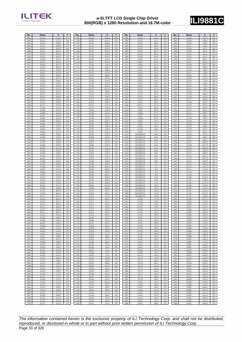
a-Si TFT LCD Single Chip Driver 800(RGB) x 1280 Resolution and 16.7M-color ILI9881C
The information contained herein is the exclusive property of ILI Technology Corp. and shall not be distributed, reproduced, or disclosed in whole or in part without prior written permission of ILI Technology Corp. Page 33 of 320
No. Name X Y No. Name X Y No. Name X Y No. Name X Y
1601 S1436 2722.5 275 1701 S1336 1622.5 365 1801 S1236 522.5 185 1901 S1160 -577.5 275
1602 S1435 2711.5 365 1702 S1335 1611.5 185 1802 S1235 511.5 275 1902 S1159 -588.5 365
1603 S1434 2700.5 185 1703 S1334 1600.5 275 1803 S1234 500.5 365 1903 S1158 -599.5 185
1604 S1433 2689.5 275 1704 S1333 1589.5 365 1804 S1233 489.5 185 1904 S1157 -610.5 275
1605 S1432 2678.5 365 1705 S1332 1578.5 185 1805 S1232 478.5 275 1905 S1156 -621.5 365
1606 S1431 2667.5 185 1706 S1331 1567.5 275 1806 S1231 467.5 365 1906 S1155 -632.5 185
1607 S1430 2656.5 275 1707 S1330 1556.5 365 1807 S1230 456.5 185 1907 S1154 -643.5 275
1608 S1429 2645.5 365 1708 S1329 1545.5 185 1808 S1229 445.5 275 1908 S1153 -654.5 365
1609 S1428 2634.5 185 1709 S1328 1534.5 275 1809 S1228 434.5 365 1909 S1152 -665.5 185
1610 S1427 2623.5 275 1710 S1327 1523.5 365 1810 S1227 423.5 185 1910 S1151 -676.5 275
1611 S1426 2612.5 365 1711 S1326 1512.5 185 1811 S1226 412.5 275 1911 S1150 -687.5 365
1612 S1425 2601.5 185 1712 S1325 1501.5 275 1812 S1225 401.5 365 1912 S1149 -698.5 185
1613 S1424 2590.5 275 1713 S1324 1490.5 365 1813 S1224 390.5 185 1913 S1148 -709.5 275
1614 S1423 2579.5 365 1714 S1323 1479.5 185 1814 S1223 379.5 275 1914 S1147 -720.5 365
1615 S1422 2568.5 185 1715 S1322 1468.5 275 1815 S1222 368.5 365 1915 S1146 -731.5 185
1616 S1421 2557.5 275 1716 S1321 1457.5 365 1816 S1221 357.5 185 1916 S1145 -742.5 275
1617 S1420 2546.5 365 1717 S1320 1446.5 185 1817 S1220 346.5 275 1917 S1144 -753.5 365
1618 S1419 2535.5 185 1718 S1319 1435.5 275 1818 S1219 335.5 365 1918 S1143 -764.5 185
1619 S1418 2524.5 275 1719 S1318 1424.5 365 1819 S1218 324.5 185 1919 S1142 -775.5 275
1620 S1417 2513.5 365 1720 S1317 1413.5 185 1820 S1217 313.5 275 1920 S1141 -786.5 365
1621 S1416 2502.5 185 1721 S1316 1402.5 275 1821 S1216 302.5 365 1921 S1140 -797.5 185
1622 S1415 2491.5 275 1722 S1315 1391.5 365 1822 S1215 291.5 185 1922 S1139 -808.5 275
1623 S1414 2480.5 365 1723 S1314 1380.5 185 1823 S1214 280.5 275 1923 S1138 -819.5 365
1624 S1413 2469.5 185 1724 S1313 1369.5 275 1824 S1213 269.5 365 1924 S1137 -830.5 185
1625 S1412 2458.5 275 1725 S1312 1358.5 365 1825 S1212 258.5 185 1925 S1136 -841.5 275
1626 S1411 2447.5 365 1726 S1311 1347.5 185 1826 S1211 247.5 275 1926 S1135 -852.5 365
1627 S1410 2436.5 185 1727 S1310 1336.5 275 1827 S1210 236.5 365 1927 S1134 -863.5 185
1628 S1409 2425.5 275 1728 S1309 1325.5 365 1828 S1209 225.5 185 1928 S1133 -874.5 275
1629 S1408 2414.5 365 1729 S1308 1314.5 185 1829 S1208 214.5 275 1929 S1132 -885.5 365
1630 S1407 2403.5 185 1730 S1307 1303.5 275 1830 S1207 203.5 365 1930 S1131 -896.5 185
1631 S1406 2392.5 275 1731 S1306 1292.5 365 1831 S1206 192.5 185 1931 S1130 -907.5 275
1632 S1405 2381.5 365 1732 S1305 1281.5 185 1832 S1205 181.5 275 1932 S1129 -918.5 365
1633 S1404 2370.5 185 1733 S1304 1270.5 275 1833 S1204 170.5 365 1933 S1128 -929.5 185
1634 S1403 2359.5 275 1734 S1303 1259.5 365 1834 S1203 159.5 185 1934 S1127 -940.5 275
1635 S1402 2348.5 365 1735 S1302 1248.5 185 1835 S1202 148.5 275 1935 S1126 -951.5 365
1636 S1401 2337.5 185 1736 S1301 1237.5 275 1836 S1201 137.5 365 1936 S1125 -962.5 185
1637 S1400 2326.5 275 1737 S1300 1226.5 365 1837 DUMMY29 126.5 185 1937 S1124 -973.5 275
1638 S1399 2315.5 365 1738 S1299 1215.5 185 1838 DUMMY30 115.5 275 1938 S1123 -984.5 365
1639 S1398 2304.5 185 1739 S1298 1204.5 275 1839 DUMMY31 104.5 365 1939 S1122 -995.5 185
1640 S1397 2293.5 275 1740 S1297 1193.5 365 1840 DUMMY32 93.5 185 1940 S1121 -1006.5 275
1641 S1396 2282.5 365 1741 S1296 1182.5 185 1841 DUMMY33 82.5 275 1941 S1120 -1017.5 365
1642 S1395 2271.5 185 1742 S1295 1171.5 275 1842 DUMMY34 71.5 365 1942 S1119 -1028.5 185
1643 S1394 2260.5 275 1743 S1294 1160.5 365 1843 DUMMY35 60.5 185 1943 S1118 -1039.5 275
1644 S1393 2249.5 365 1744 S1293 1149.5 185 1844 DUMMY36 49.5 275 1944 S1117 -1050.5 365
1645 S1392 2238.5 185 1745 S1292 1138.5 275 1845 DUMMY37 38.5 365 1945 S1116 -1061.5 185
1646 S1391 2227.5 275 1746 S1291 1127.5 365 1846 DUMMY38 27.5 185 1946 S1115 -1072.5 275
1647 S1390 2216.5 365 1747 S1290 1116.5 185 1847 DUMMY39 16.5 275 1947 S1114 -1083.5 365
1648 S1389 2205.5 185 1748 S1289 1105.5 275 1848 DUMMY40 5.5 365 1948 S1113 -1094.5 185
1649 S1388 2194.5 275 1749 S1288 1094.5 365 1849 DUMMY41 -5.5 185 1949 S1112 -1105.5 275
1650 S1387 2183.5 365 1750 S1287 1083.5 185 1850 DUMMY42 -16.5 275 1950 S1111 -1116.5 365
1651 S1386 2172.5 185 1751 S1286 1072.5 275 1851 DUMMY43 -27.5 365 1951 S1110 -1127.5 185
1652 S1385 2161.5 275 1752 S1285 1061.5 365 1852 DUMMY44 -38.5 185 1952 S1109 -1138.5 275
1653 S1384 2150.5 365 1753 S1284 1050.5 185 1853 DUMMY45 -49.5 275 1953 S1108 -1149.5 365
1654 S1383 2139.5 185 1754 S1283 1039.5 275 1854 DUMMY46 -60.5 365 1954 S1107 -1160.5 185
1655 S1382 2128.5 275 1755 S1282 1028.5 365 1855 DUMMY47 -71.5 185 1955 S1106 -1171.5 275
1656 S1381 2117.5 365 1756 S1281 1017.5 185 1856 DUMMY48 -82.5 275 1956 S1105 -1182.5 365
1657 S1380 2106.5 185 1757 S1280 1006.5 275 1857 DUMMY49 -93.5 365 1957 S1104 -1193.5 185
1658 S1379 2095.5 275 1758 S1279 995.5 365 1858 DUMMY50 -104.5 185 1958 S1103 -1204.5 275
1659 S1378 2084.5 365 1759 S1278 984.5 185 1859 DUMMY51 -115.5 275 1959 S1102 -1215.5 365
1660 S1377 2073.5 185 1760 S1277 973.5 275 1860 DUMMY52 -126.5 365 1960 S1101 -1226.5 185
1661 S1376 2062.5 275 1761 S1276 962.5 365 1861 S1200 -137.5 185 1961 S1100 -1237.5 275
1662 S1375 2051.5 365 1762 S1275 951.5 185 1862 S1199 -148.5 275 1962 S1099 -1248.5 365
1663 S1374 2040.5 185 1763 S1274 940.5 275 1863 S1198 -159.5 365 1963 S1098 -1259.5 185
1664 S1373 2029.5 275 1764 S1273 929.5 365 1864 S1197 -170.5 185 1964 S1097 -1270.5 275
1665 S1372 2018.5 365 1765 S1272 918.5 185 1865 S1196 -181.5 275 1965 S1096 -1281.5 365
1666 S1371 2007.5 185 1766 S1271 907.5 275 1866 S1195 -192.5 365 1966 S1095 -1292.5 185
1667 S1370 1996.5 275 1767 S1270 896.5 365 1867 S1194 -203.5 185 1967 S1094 -1303.5 275
1668 S1369 1985.5 365 1768 S1269 885.5 185 1868 S1193 -214.5 275 1968 S1093 -1314.5 365
1669 S1368 1974.5 185 1769 S1268 874.5 275 1869 S1192 -225.5 365 1969 S1092 -1325.5 185
1670 S1367 1963.5 275 1770 S1267 863.5 365 1870 S1191 -236.5 185 1970 S1091 -1336.5 275
1671 S1366 1952.5 365 1771 S1266 852.5 185 1871 S1190 -247.5 275 1971 S1090 -1347.5 365
1672 S1365 1941.5 185 1772 S1265 841.5 275 1872 S1189 -258.5 365 1972 S1089 -1358.5 185
1673 S1364 1930.5 275 1773 S1264 830.5 365 1873 S1188 -269.5 185 1973 S1088 -1369.5 275
1674 S1363 1919.5 365 1774 S1263 819.5 185 1874 S1187 -280.5 275 1974 S1087 -1380.5 365
1675 S1362 1908.5 185 1775 S1262 808.5 275 1875 S1186 -291.5 365 1975 S1086 -1391.5 185
1676 S1361 1897.5 275 1776 S1261 797.5 365 1876 S1185 -302.5 185 1976 S1085 -1402.5 275
1677 S1360 1886.5 365 1777 S1260 786.5 185 1877 S1184 -313.5 275 1977 S1084 -1413.5 365
1678 S1359 1875.5 185 1778 S1259 775.5 275 1878 S1183 -324.5 365 1978 S1083 -1424.5 185
1679 S1358 1864.5 275 1779 S1258 764.5 365 1879 S1182 -335.5 185 1979 S1082 -1435.5 275
1680 S1357 1853.5 365 1780 S1257 753.5 185 1880 S1181 -346.5 275 1980 S1081 -1446.5 365
1681 S1356 1842.5 185 1781 S1256 742.5 275 1881 S1180 -357.5 365 1981 S1080 -1457.5 185
1682 S1355 1831.5 275 1782 S1255 731.5 365 1882 S1179 -368.5 185 1982 S1079 -1468.5 275
1683 S1354 1820.5 365 1783 S1254 720.5 185 1883 S1178 -379.5 275 1983 S1078 -1479.5 365
1684 S1353 1809.5 185 1784 S1253 709.5 275 1884 S1177 -390.5 365 1984 S1077 -1490.5 185
1685 S1352 1798.5 275 1785 S1252 698.5 365 1885 S1176 -401.5 185 1985 S1076 -1501.5 275
1686 S1351 1787.5 365 1786 S1251 687.5 185 1886 S1175 -412.5 275 1986 S1075 -1512.5 365
1687 S1350 1776.5 185 1787 S1250 676.5 275 1887 S1174 -423.5 365 1987 S1074 -1523.5 185
1688 S1349 1765.5 275 1788 S1249 665.5 365 1888 S1173 -434.5 185 1988 S1073 -1534.5 275
1689 S1348 1754.5 365 1789 S1248 654.5 185 1889 S1172 -445.5 275 1989 S1072 -1545.5 365
1690 S1347 1743.5 185 1790 S1247 643.5 275 1890 S1171 -456.5 365 1990 S1071 -1556.5 185
1691 S1346 1732.5 275 1791 S1246 632.5 365 1891 S1170 -467.5 185 1991 S1070 -1567.5 275
1692 S1345 1721.5 365 1792 S1245 621.5 185 1892 S1169 -478.5 275 1992 S1069 -1578.5 365
1693 S1344 1710.5 185 1793 S1244 610.5 275 1893 S1168 -489.5 365 1993 S1068 -1589.5 185
1694 S1343 1699.5 275 1794 S1243 599.5 365 1894 S1167 -500.5 185 1994 S1067 -1600.5 275
1695 S1342 1688.5 365 1795 S1242 588.5 185 1895 S1166 -511.5 275 1995 S1066 -1611.5 365
1696 S1341 1677.5 185 1796 S1241 577.5 275 1896 S1165 -522.5 365 1996 S1065 -1622.5 185
1697 S1340 1666.5 275 1797 S1240 566.5 365 1897 S1164 -533.5 185 1997 S1064 -1633.5 275
1698 S1339 1655.5 365 1798 S1239 555.5 185 1898 S1163 -544.5 275 1998 S1063 -1644.5 365
1699 S1338 1644.5 185 1799 S1238 544.5 275 1899 S1162 -555.5 365 1999 S1062 -1655.5 185
1700 S1337 1633.5 275 1800 S1237 533.5 365 1900 S1161 -566.5 185 2000 S1061 -1666.5 275

a-Si TFT LCD Single Chip Driver 800(RGB) x 1280 Resolution and 16.7M-color ILI9881C
The information contained herein is the exclusive property of ILI Technology Corp. and shall not be distributed, reproduced, or disclosed in whole or in part without prior written permission of ILI Technology Corp. Page 34 of 320
No. Name X Y No. Name X Y No. Name X Y No. Name X Y
2001 S1060 -1677.5 365 2101 S960 -2777.5 185 2201 S860 -3877.5 275 2301 S760 -4977.5 365
2002 S1059 -1688.5 185 2102 S959 -2788.5 275 2202 S859 -3888.5 365 2302 S759 -4988.5 185
2003 S1058 -1699.5 275 2103 S958 -2799.5 365 2203 S858 -3899.5 185 2303 S758 -4999.5 275
2004 S1057 -1710.5 365 2104 S957 -2810.5 185 2204 S857 -3910.5 275 2304 S757 -5010.5 365
2005 S1056 -1721.5 185 2105 S956 -2821.5 275 2205 S856 -3921.5 365 2305 S756 -5021.5 185
2006 S1055 -1732.5 275 2106 S955 -2832.5 365 2206 S855 -3932.5 185 2306 S755 -5032.5 275
2007 S1054 -1743.5 365 2107 S954 -2843.5 185 2207 S854 -3943.5 275 2307 S754 -5043.5 365
2008 S1053 -1754.5 185 2108 S953 -2854.5 275 2208 S853 -3954.5 365 2308 S753 -5054.5 185
2009 S1052 -1765.5 275 2109 S952 -2865.5 365 2209 S852 -3965.5 185 2309 S752 -5065.5 275
2010 S1051 -1776.5 365 2110 S951 -2876.5 185 2210 S851 -3976.5 275 2310 S751 -5076.5 365
2011 S1050 -1787.5 185 2111 S950 -2887.5 275 2211 S850 -3987.5 365 2311 S750 -5087.5 185
2012 S1049 -1798.5 275 2112 S949 -2898.5 365 2212 S849 -3998.5 185 2312 S749 -5098.5 275
2013 S1048 -1809.5 365 2113 S948 -2909.5 185 2213 S848 -4009.5 275 2313 S748 -5109.5 365
2014 S1047 -1820.5 185 2114 S947 -2920.5 275 2214 S847 -4020.5 365 2314 S747 -5120.5 185
2015 S1046 -1831.5 275 2115 S946 -2931.5 365 2215 S846 -4031.5 185 2315 S746 -5131.5 275
2016 S1045 -1842.5 365 2116 S945 -2942.5 185 2216 S845 -4042.5 275 2316 S745 -5142.5 365
2017 S1044 -1853.5 185 2117 S944 -2953.5 275 2217 S844 -4053.5 365 2317 S744 -5153.5 185
2018 S1043 -1864.5 275 2118 S943 -2964.5 365 2218 S843 -4064.5 185 2318 S743 -5164.5 275
2019 S1042 -1875.5 365 2119 S942 -2975.5 185 2219 S842 -4075.5 275 2319 S742 -5175.5 365
2020 S1041 -1886.5 185 2120 S941 -2986.5 275 2220 S841 -4086.5 365 2320 S741 -5186.5 185
2021 S1040 -1897.5 275 2121 S940 -2997.5 365 2221 S840 -4097.5 185 2321 S740 -5197.5 275
2022 S1039 -1908.5 365 2122 S939 -3008.5 185 2222 S839 -4108.5 275 2322 S739 -5208.5 365
2023 S1038 -1919.5 185 2123 S938 -3019.5 275 2223 S838 -4119.5 365 2323 S738 -5219.5 185
2024 S1037 -1930.5 275 2124 S937 -3030.5 365 2224 S837 -4130.5 185 2324 S737 -5230.5 275
2025 S1036 -1941.5 365 2125 S936 -3041.5 185 2225 S836 -4141.5 275 2325 S736 -5241.5 365
2026 S1035 -1952.5 185 2126 S935 -3052.5 275 2226 S835 -4152.5 365 2326 S735 -5252.5 185
2027 S1034 -1963.5 275 2127 S934 -3063.5 365 2227 S834 -4163.5 185 2327 S734 -5263.5 275
2028 S1033 -1974.5 365 2128 S933 -3074.5 185 2228 S833 -4174.5 275 2328 S733 -5274.5 365
2029 S1032 -1985.5 185 2129 S932 -3085.5 275 2229 S832 -4185.5 365 2329 S732 -5285.5 185
2030 S1031 -1996.5 275 2130 S931 -3096.5 365 2230 S831 -4196.5 185 2330 S731 -5296.5 275
2031 S1030 -2007.5 365 2131 S930 -3107.5 185 2231 S830 -4207.5 275 2331 S730 -5307.5 365
2032 S1029 -2018.5 185 2132 S929 -3118.5 275 2232 S829 -4218.5 365 2332 S729 -5318.5 185
2033 S1028 -2029.5 275 2133 S928 -3129.5 365 2233 S828 -4229.5 185 2333 S728 -5329.5 275
2034 S1027 -2040.5 365 2134 S927 -3140.5 185 2234 S827 -4240.5 275 2334 S727 -5340.5 365
2035 S1026 -2051.5 185 2135 S926 -3151.5 275 2235 S826 -4251.5 365 2335 S726 -5351.5 185
2036 S1025 -2062.5 275 2136 S925 -3162.5 365 2236 S825 -4262.5 185 2336 S725 -5362.5 275
2037 S1024 -2073.5 365 2137 S924 -3173.5 185 2237 S824 -4273.5 275 2337 S724 -5373.5 365
2038 S1023 -2084.5 185 2138 S923 -3184.5 275 2238 S823 -4284.5 365 2338 S723 -5384.5 185
2039 S1022 -2095.5 275 2139 S922 -3195.5 365 2239 S822 -4295.5 185 2339 S722 -5395.5 275
2040 S1021 -2106.5 365 2140 S921 -3206.5 185 2240 S821 -4306.5 275 2340 S721 -5406.5 365
2041 S1020 -2117.5 185 2141 S920 -3217.5 275 2241 S820 -4317.5 365 2341 S720 -5417.5 185
2042 S1019 -2128.5 275 2142 S919 -3228.5 365 2242 S819 -4328.5 185 2342 S719 -5428.5 275
2043 S1018 -2139.5 365 2143 S918 -3239.5 185 2243 S818 -4339.5 275 2343 S718 -5439.5 365
2044 S1017 -2150.5 185 2144 S917 -3250.5 275 2244 S817 -4350.5 365 2344 S717 -5450.5 185
2045 S1016 -2161.5 275 2145 S916 -3261.5 365 2245 S816 -4361.5 185 2345 S716 -5461.5 275
2046 S1015 -2172.5 365 2146 S915 -3272.5 185 2246 S815 -4372.5 275 2346 S715 -5472.5 365
2047 S1014 -2183.5 185 2147 S914 -3283.5 275 2247 S814 -4383.5 365 2347 S714 -5483.5 185
2048 S1013 -2194.5 275 2148 S913 -3294.5 365 2248 S813 -4394.5 185 2348 S713 -5494.5 275
2049 S1012 -2205.5 365 2149 S912 -3305.5 185 2249 S812 -4405.5 275 2349 S712 -5505.5 365
2050 S1011 -2216.5 185 2150 S911 -3316.5 275 2250 S811 -4416.5 365 2350 S711 -5516.5 185
2051 S1010 -2227.5 275 2151 S910 -3327.5 365 2251 S810 -4427.5 185 2351 S710 -5527.5 275
2052 S1009 -2238.5 365 2152 S909 -3338.5 185 2252 S809 -4438.5 275 2352 S709 -5538.5 365
2053 S1008 -2249.5 185 2153 S908 -3349.5 275 2253 S808 -4449.5 365 2353 S708 -5549.5 185
2054 S1007 -2260.5 275 2154 S907 -3360.5 365 2254 S807 -4460.5 185 2354 S707 -5560.5 275
2055 S1006 -2271.5 365 2155 S906 -3371.5 185 2255 S806 -4471.5 275 2355 S706 -5571.5 365
2056 S1005 -2282.5 185 2156 S905 -3382.5 275 2256 S805 -4482.5 365 2356 S705 -5582.5 185
2057 S1004 -2293.5 275 2157 S904 -3393.5 365 2257 S804 -4493.5 185 2357 S704 -5593.5 275
2058 S1003 -2304.5 365 2158 S903 -3404.5 185 2258 S803 -4504.5 275 2358 S703 -5604.5 365
2059 S1002 -2315.5 185 2159 S902 -3415.5 275 2259 S802 -4515.5 365 2359 S702 -5615.5 185
2060 S1001 -2326.5 275 2160 S901 -3426.5 365 2260 S801 -4526.5 185 2360 S701 -5626.5 275
2061 S1000 -2337.5 365 2161 S900 -3437.5 185 2261 S800 -4537.5 275 2361 S700 -5637.5 365
2062 S999 -2348.5 185 2162 S899 -3448.5 275 2262 S799 -4548.5 365 2362 S699 -5648.5 185
2063 S998 -2359.5 275 2163 S898 -3459.5 365 2263 S798 -4559.5 185 2363 S698 -5659.5 275
2064 S997 -2370.5 365 2164 S897 -3470.5 185 2264 S797 -4570.5 275 2364 S697 -5670.5 365
2065 S996 -2381.5 185 2165 S896 -3481.5 275 2265 S796 -4581.5 365 2365 S696 -5681.5 185
2066 S995 -2392.5 275 2166 S895 -3492.5 365 2266 S795 -4592.5 185 2366 S695 -5692.5 275
2067 S994 -2403.5 365 2167 S894 -3503.5 185 2267 S794 -4603.5 275 2367 S694 -5703.5 365
2068 S993 -2414.5 185 2168 S893 -3514.5 275 2268 S793 -4614.5 365 2368 S693 -5714.5 185
2069 S992 -2425.5 275 2169 S892 -3525.5 365 2269 S792 -4625.5 185 2369 S692 -5725.5 275
2070 S991 -2436.5 365 2170 S891 -3536.5 185 2270 S791 -4636.5 275 2370 S691 -5736.5 365
2071 S990 -2447.5 185 2171 S890 -3547.5 275 2271 S790 -4647.5 365 2371 S690 -5747.5 185
2072 S989 -2458.5 275 2172 S889 -3558.5 365 2272 S789 -4658.5 185 2372 S689 -5758.5 275
2073 S988 -2469.5 365 2173 S888 -3569.5 185 2273 S788 -4669.5 275 2373 S688 -5769.5 365
2074 S987 -2480.5 185 2174 S887 -3580.5 275 2274 S787 -4680.5 365 2374 S687 -5780.5 185
2075 S986 -2491.5 275 2175 S886 -3591.5 365 2275 S786 -4691.5 185 2375 S686 -5791.5 275
2076 S985 -2502.5 365 2176 S885 -3602.5 185 2276 S785 -4702.5 275 2376 S685 -5802.5 365
2077 S984 -2513.5 185 2177 S884 -3613.5 275 2277 S784 -4713.5 365 2377 S684 -5813.5 185
2078 S983 -2524.5 275 2178 S883 -3624.5 365 2278 S783 -4724.5 185 2378 S683 -5824.5 275
2079 S982 -2535.5 365 2179 S882 -3635.5 185 2279 S782 -4735.5 275 2379 S682 -5835.5 365
2080 S981 -2546.5 185 2180 S881 -3646.5 275 2280 S781 -4746.5 365 2380 S681 -5846.5 185
2081 S980 -2557.5 275 2181 S880 -3657.5 365 2281 S780 -4757.5 185 2381 S680 -5857.5 275
2082 S979 -2568.5 365 2182 S879 -3668.5 185 2282 S779 -4768.5 275 2382 S679 -5868.5 365
2083 S978 -2579.5 185 2183 S878 -3679.5 275 2283 S778 -4779.5 365 2383 S678 -5879.5 185
2084 S977 -2590.5 275 2184 S877 -3690.5 365 2284 S777 -4790.5 185 2384 S677 -5890.5 275
2085 S976 -2601.5 365 2185 S876 -3701.5 185 2285 S776 -4801.5 275 2385 S676 -5901.5 365
2086 S975 -2612.5 185 2186 S875 -3712.5 275 2286 S775 -4812.5 365 2386 S675 -5912.5 185
2087 S974 -2623.5 275 2187 S874 -3723.5 365 2287 S774 -4823.5 185 2387 S674 -5923.5 275
2088 S973 -2634.5 365 2188 S873 -3734.5 185 2288 S773 -4834.5 275 2388 S673 -5934.5 365
2089 S972 -2645.5 185 2189 S872 -3745.5 275 2289 S772 -4845.5 365 2389 S672 -5945.5 185
2090 S971 -2656.5 275 2190 S871 -3756.5 365 2290 S771 -4856.5 185 2390 S671 -5956.5 275
2091 S970 -2667.5 365 2191 S870 -3767.5 185 2291 S770 -4867.5 275 2391 S670 -5967.5 365
2092 S969 -2678.5 185 2192 S869 -3778.5 275 2292 S769 -4878.5 365 2392 S669 -5978.5 185
2093 S968 -2689.5 275 2193 S868 -3789.5 365 2293 S768 -4889.5 185 2393 S668 -5989.5 275
2094 S967 -2700.5 365 2194 S867 -3800.5 185 2294 S767 -4900.5 275 2394 S667 -6000.5 365
2095 S966 -2711.5 185 2195 S866 -3811.5 275 2295 S766 -4911.5 365 2395 S666 -6011.5 185
2096 S965 -2722.5 275 2196 S865 -3822.5 365 2296 S765 -4922.5 185 2396 S665 -6022.5 275
2097 S964 -2733.5 365 2197 S864 -3833.5 185 2297 S764 -4933.5 275 2397 S664 -6033.5 365
2098 S963 -2744.5 185 2198 S863 -3844.5 275 2298 S763 -4944.5 365 2398 S663 -6044.5 185
2099 S962 -2755.5 275 2199 S862 -3855.5 365 2299 S762 -4955.5 185 2399 S662 -6055.5 275
2100 S961 -2766.5 365 2200 S861 -3866.5 185 2300 S761 -4966.5 275 2400 S661 -6066.5 365

a-Si TFT LCD Single Chip Driver 800(RGB) x 1280 Resolution and 16.7M-color ILI9881C
The information contained herein is the exclusive property of ILI Technology Corp. and shall not be distributed, reproduced, or disclosed in whole or in part without prior written permission of ILI Technology Corp. Page 35 of 320
No. Name X Y No. Name X Y No. Name X Y No. Name X Y
2401 S660 -6077.5 185 2501 S578 -7177.5 275 2601 S478 -8277.5 365 2701 S378 -9377.5 185
2402 S659 -6088.5 275 2502 S577 -7188.5 365 2602 S477 -8288.5 185 2702 S377 -9388.5 275
2403 S658 -6099.5 365 2503 S576 -7199.5 185 2603 S476 -8299.5 275 2703 S376 -9399.5 365
2404 S657 -6110.5 185 2504 S575 -7210.5 275 2604 S475 -8310.5 365 2704 S375 -9410.5 185
2405 S656 -6121.5 275 2505 S574 -7221.5 365 2605 S474 -8321.5 185 2705 S374 -9421.5 275
2406 S655 -6132.5 365 2506 S573 -7232.5 185 2606 S473 -8332.5 275 2706 S373 -9432.5 365
2407 S654 -6143.5 185 2507 S572 -7243.5 275 2607 S472 -8343.5 365 2707 S372 -9443.5 185
2408 S653 -6154.5 275 2508 S571 -7254.5 365 2608 S471 -8354.5 185 2708 S371 -9454.5 275
2409 S652 -6165.5 365 2509 S570 -7265.5 185 2609 S470 -8365.5 275 2709 S370 -9465.5 365
2410 S651 -6176.5 185 2510 S569 -7276.5 275 2610 S469 -8376.5 365 2710 S369 -9476.5 185
2411 S650 -6187.5 275 2511 S568 -7287.5 365 2611 S468 -8387.5 185 2711 S368 -9487.5 275
2412 S649 -6198.5 365 2512 S567 -7298.5 185 2612 S467 -8398.5 275 2712 S367 -9498.5 365
2413 S648 -6209.5 185 2513 S566 -7309.5 275 2613 S466 -8409.5 365 2713 S366 -9509.5 185
2414 S647 -6220.5 275 2514 S565 -7320.5 365 2614 S465 -8420.5 185 2714 S365 -9520.5 275
2415 S646 -6231.5 365 2515 S564 -7331.5 185 2615 S464 -8431.5 275 2715 S364 -9531.5 365
2416 S645 -6242.5 185 2516 S563 -7342.5 275 2616 S463 -8442.5 365 2716 S363 -9542.5 185
2417 S644 -6253.5 275 2517 S562 -7353.5 365 2617 S462 -8453.5 185 2717 S362 -9553.5 275
2418 S643 -6264.5 365 2518 S561 -7364.5 185 2618 S461 -8464.5 275 2718 S361 -9564.5 365
2419 S642 -6275.5 185 2519 S560 -7375.5 275 2619 S460 -8475.5 365 2719 S360 -9575.5 185
2420 S641 -6286.5 275 2520 S559 -7386.5 365 2620 S459 -8486.5 185 2720 S359 -9586.5 275
2421 S640 -6297.5 365 2521 S558 -7397.5 185 2621 S458 -8497.5 275 2721 S358 -9597.5 365
2422 S639 -6308.5 185 2522 S557 -7408.5 275 2622 S457 -8508.5 365 2722 S357 -9608.5 185
2423 S638 -6319.5 275 2523 S556 -7419.5 365 2623 S456 -8519.5 185 2723 S356 -9619.5 275
2424 S637 -6330.5 365 2524 S555 -7430.5 185 2624 S455 -8530.5 275 2724 S355 -9630.5 365
2425 S636 -6341.5 185 2525 S554 -7441.5 275 2625 S454 -8541.5 365 2725 S354 -9641.5 185
2426 S635 -6352.5 275 2526 S553 -7452.5 365 2626 S453 -8552.5 185 2726 S353 -9652.5 275
2427 S634 -6363.5 365 2527 S552 -7463.5 185 2627 S452 -8563.5 275 2727 S352 -9663.5 365
2428 S633 -6374.5 185 2528 S551 -7474.5 275 2628 S451 -8574.5 365 2728 S351 -9674.5 185
2429 S632 -6385.5 275 2529 S550 -7485.5 365 2629 S450 -8585.5 185 2729 S350 -9685.5 275
2430 S631 -6396.5 365 2530 S549 -7496.5 185 2630 S449 -8596.5 275 2730 S349 -9696.5 365
2431 S630 -6407.5 185 2531 S548 -7507.5 275 2631 S448 -8607.5 365 2731 S348 -9707.5 185
2432 S629 -6418.5 275 2532 S547 -7518.5 365 2632 S447 -8618.5 185 2732 S347 -9718.5 275
2433 S628 -6429.5 365 2533 S546 -7529.5 185 2633 S446 -8629.5 275 2733 S346 -9729.5 365
2434 S627 -6440.5 185 2534 S545 -7540.5 275 2634 S445 -8640.5 365 2734 S345 -9740.5 185
2435 S626 -6451.5 275 2535 S544 -7551.5 365 2635 S444 -8651.5 185 2735 S344 -9751.5 275
2436 S625 -6462.5 365 2536 S543 -7562.5 185 2636 S443 -8662.5 275 2736 S343 -9762.5 365
2437 S624 -6473.5 185 2537 S542 -7573.5 275 2637 S442 -8673.5 365 2737 S342 -9773.5 185
2438 S623 -6484.5 275 2538 S541 -7584.5 365 2638 S441 -8684.5 185 2738 S341 -9784.5 275
2439 S622 -6495.5 365 2539 S540 -7595.5 185 2639 S440 -8695.5 275 2739 S340 -9795.5 365
2440 S621 -6506.5 185 2540 S539 -7606.5 275 2640 S439 -8706.5 365 2740 S339 -9806.5 185
2441 S620 -6517.5 275 2541 S538 -7617.5 365 2641 S438 -8717.5 185 2741 S338 -9817.5 275
2442 S619 -6528.5 365 2542 S537 -7628.5 185 2642 S437 -8728.5 275 2742 S337 -9828.5 365
2443 S618 -6539.5 185 2543 S536 -7639.5 275 2643 S436 -8739.5 365 2743 S336 -9839.5 185
2444 S617 -6550.5 275 2544 S535 -7650.5 365 2644 S435 -8750.5 185 2744 S335 -9850.5 275
2445 S616 -6561.5 365 2545 S534 -7661.5 185 2645 S434 -8761.5 275 2745 S334 -9861.5 365
2446 S615 -6572.5 185 2546 S533 -7672.5 275 2646 S433 -8772.5 365 2746 S333 -9872.5 185
2447 S614 -6583.5 275 2547 S532 -7683.5 365 2647 S432 -8783.5 185 2747 S332 -9883.5 275
2448 S613 -6594.5 365 2548 S531 -7694.5 185 2648 S431 -8794.5 275 2748 S331 -9894.5 365
2449 S612 -6605.5 185 2549 S530 -7705.5 275 2649 S430 -8805.5 365 2749 S330 -9905.5 185
2450 S611 -6616.5 275 2550 S529 -7716.5 365 2650 S429 -8816.5 185 2750 S329 -9916.5 275
2451 S610 -6627.5 365 2551 S528 -7727.5 185 2651 S428 -8827.5 275 2751 S328 -9927.5 365
2452 S609 -6638.5 185 2552 S527 -7738.5 275 2652 S427 -8838.5 365 2752 S327 -9938.5 185
2453 S608 -6649.5 275 2553 S526 -7749.5 365 2653 S426 -8849.5 185 2753 S326 -9949.5 275
2454 S607 -6660.5 365 2554 S525 -7760.5 185 2654 S425 -8860.5 275 2754 S325 -9960.5 365
2455 S606 -6671.5 185 2555 S524 -7771.5 275 2655 S424 -8871.5 365 2755 S324 -9971.5 185
2456 S605 -6682.5 275 2556 S523 -7782.5 365 2656 S423 -8882.5 185 2756 S323 -9982.5 275
2457 S604 -6693.5 365 2557 S522 -7793.5 185 2657 S422 -8893.5 275 2757 S322 -9993.5 365
2458 S603 -6704.5 185 2558 S521 -7804.5 275 2658 S421 -8904.5 365 2758 S321 -10004.5 185
2459 S602 -6715.5 275 2559 S520 -7815.5 365 2659 S420 -8915.5 185 2759 S320 -10015.5 275
2460 S601 -6726.5 365 2560 S519 -7826.5 185 2660 S419 -8926.5 275 2760 S319 -10026.5 365
2461 DUMMY53 -6737.5 185 2561 S518 -7837.5 275 2661 S418 -8937.5 365 2761 S318 -10037.5 185
2462 DUMMY54 -6748.5 275 2562 S517 -7848.5 365 2662 S417 -8948.5 185 2762 S317 -10048.5 275
2463 DUMMY55 -6759.5 365 2563 S516 -7859.5 185 2663 S416 -8959.5 275 2763 S316 -10059.5 365
2464 DUMMY56 -6770.5 185 2564 S515 -7870.5 275 2664 S415 -8970.5 365 2764 S315 -10070.5 185
2465 DUMMY57 -6781.5 275 2565 S514 -7881.5 365 2665 S414 -8981.5 185 2765 S314 -10081.5 275
2466 DUMMY58 -6792.5 365 2566 S513 -7892.5 185 2666 S413 -8992.5 275 2766 S313 -10092.5 365
2467 DUMMY59 -6803.5 185 2567 S512 -7903.5 275 2667 S412 -9003.5 365 2767 S312 -10103.5 185
2468 DUMMY60 -6814.5 275 2568 S511 -7914.5 365 2668 S411 -9014.5 185 2768 S311 -10114.5 275
2469 DUMMY61 -6825.5 365 2569 S510 -7925.5 185 2669 S410 -9025.5 275 2769 S310 -10125.5 365
2470 DUMMY62 -6836.5 185 2570 S509 -7936.5 275 2670 S409 -9036.5 365 2770 S309 -10136.5 185
2471 DUMMY63 -6847.5 275 2571 S508 -7947.5 365 2671 S408 -9047.5 185 2771 S308 -10147.5 275
2472 DUMMY64 -6858.5 365 2572 S507 -7958.5 185 2672 S407 -9058.5 275 2772 S307 -10158.5 365
2473 DUMMY65 -6869.5 185 2573 S506 -7969.5 275 2673 S406 -9069.5 365 2773 S306 -10169.5 185
2474 DUMMY66 -6880.5 275 2574 S505 -7980.5 365 2674 S405 -9080.5 185 2774 S305 -10180.5 275
2475 DUMMY67 -6891.5 365 2575 S504 -7991.5 185 2675 S404 -9091.5 275 2775 S304 -10191.5 365
2476 DUMMY68 -6902.5 185 2576 S503 -8002.5 275 2676 S403 -9102.5 365 2776 S303 -10202.5 185
2477 DUMMY69 -6913.5 275 2577 S502 -8013.5 365 2677 S402 -9113.5 185 2777 S302 -10213.5 275
2478 DUMMY70 -6924.5 365 2578 S501 -8024.5 185 2678 S401 -9124.5 275 2778 S301 -10224.5 365
2479 S600 -6935.5 185 2579 S500 -8035.5 275 2679 S400 -9135.5 365 2779 S300 -10235.5 185
2480 S599 -6946.5 275 2580 S499 -8046.5 365 2680 S399 -9146.5 185 2780 S299 -10246.5 275
2481 S598 -6957.5 365 2581 S498 -8057.5 185 2681 S398 -9157.5 275 2781 S298 -10257.5 365
2482 S597 -6968.5 185 2582 S497 -8068.5 275 2682 S397 -9168.5 365 2782 S297 -10268.5 185
2483 S596 -6979.5 275 2583 S496 -8079.5 365 2683 S396 -9179.5 185 2783 S296 -10279.5 275
2484 S595 -6990.5 365 2584 S495 -8090.5 185 2684 S395 -9190.5 275 2784 S295 -10290.5 365
2485 S594 -7001.5 185 2585 S494 -8101.5 275 2685 S394 -9201.5 365 2785 S294 -10301.5 185
2486 S593 -7012.5 275 2586 S493 -8112.5 365 2686 S393 -9212.5 185 2786 S293 -10312.5 275
2487 S592 -7023.5 365 2587 S492 -8123.5 185 2687 S392 -9223.5 275 2787 S292 -10323.5 365
2488 S591 -7034.5 185 2588 S491 -8134.5 275 2688 S391 -9234.5 365 2788 S291 -10334.5 185
2489 S590 -7045.5 275 2589 S490 -8145.5 365 2689 S390 -9245.5 185 2789 S290 -10345.5 275
2490 S589 -7056.5 365 2590 S489 -8156.5 185 2690 S389 -9256.5 275 2790 S289 -10356.5 365
2491 S588 -7067.5 185 2591 S488 -8167.5 275 2691 S388 -9267.5 365 2791 S288 -10367.5 185
2492 S587 -7078.5 275 2592 S487 -8178.5 365 2692 S387 -9278.5 185 2792 S287 -10378.5 275
2493 S586 -7089.5 365 2593 S486 -8189.5 185 2693 S386 -9289.5 275 2793 S286 -10389.5 365
2494 S585 -7100.5 185 2594 S485 -8200.5 275 2694 S385 -9300.5 365 2794 S285 -10400.5 185
2495 S584 -7111.5 275 2595 S484 -8211.5 365 2695 S384 -9311.5 185 2795 S284 -10411.5 275
2496 S583 -7122.5 365 2596 S483 -8222.5 185 2696 S383 -9322.5 275 2796 S283 -10422.5 365
2497 S582 -7133.5 185 2597 S482 -8233.5 275 2697 S382 -9333.5 365 2797 S282 -10433.5 185
2498 S581 -7144.5 275 2598 S481 -8244.5 365 2698 S381 -9344.5 185 2798 S281 -10444.5 275
2499 S580 -7155.5 365 2599 S480 -8255.5 185 2699 S380 -9355.5 275 2799 S280 -10455.5 365
2500 S579 -7166.5 185 2600 S479 -8266.5 275 2700 S379 -9366.5 365 2800 S279 -10466.5 185

a-Si TFT LCD Single Chip Driver 800(RGB) x 1280 Resolution and 16.7M-color ILI9881C
The information contained herein is the exclusive property of ILI Technology Corp. and shall not be distributed, reproduced, or disclosed in whole or in part without prior written permission of ILI Technology Corp. Page 36 of 320
No. Name X Y No. Name X Y No. Name X Y No. Name X Y
2801 S278 -10477.5 275 2901 S178 -11577.5 365 3001 S78 -12677.5 185
2802 S277 -10488.5 365 2902 S177 -11588.5 185 3002 S77 -12688.5 275
2803 S276 -10499.5 185 2903 S176 -11599.5 275 3003 S76 -12699.5 365
2804 S275 -10510.5 275 2904 S175 -11610.5 365 3004 S75 -12710.5 185
2805 S274 -10521.5 365 2905 S174 -11621.5 185 3005 S74 -12721.5 275
2806 S273 -10532.5 185 2906 S173 -11632.5 275 3006 S73 -12732.5 365
2807 S272 -10543.5 275 2907 S172 -11643.5 365 3007 S72 -12743.5 185
2808 S271 -10554.5 365 2908 S171 -11654.5 185 3008 S71 -12754.5 275
2809 S270 -10565.5 185 2909 S170 -11665.5 275 3009 S70 -12765.5 365
2810 S269 -10576.5 275 2910 S169 -11676.5 365 3010 S69 -12776.5 185
2811 S268 -10587.5 365 2911 S168 -11687.5 185 3011 S68 -12787.5 275
2812 S267 -10598.5 185 2912 S167 -11698.5 275 3012 S67 -12798.5 365
2813 S266 -10609.5 275 2913 S166 -11709.5 365 3013 S66 -12809.5 185
2814 S265 -10620.5 365 2914 S165 -11720.5 185 3014 S65 -12820.5 275
2815 S264 -10631.5 185 2915 S164 -11731.5 275 3015 S64 -12831.5 365
2816 S263 -10642.5 275 2916 S163 -11742.5 365 3016 S63 -12842.5 185
2817 S262 -10653.5 365 2917 S162 -11753.5 185 3017 S62 -12853.5 275
2818 S261 -10664.5 185 2918 S161 -11764.5 275 3018 S61 -12864.5 365
2819 S260 -10675.5 275 2919 S160 -11775.5 365 3019 S60 -12875.5 185
2820 S259 -10686.5 365 2920 S159 -11786.5 185 3020 S59 -12886.5 275
2821 S258 -10697.5 185 2921 S158 -11797.5 275 3021 S58 -12897.5 365
2822 S257 -10708.5 275 2922 S157 -11808.5 365 3022 S57 -12908.5 185
2823 S256 -10719.5 365 2923 S156 -11819.5 185 3023 S56 -12919.5 275
2824 S255 -10730.5 185 2924 S155 -11830.5 275 3024 S55 -12930.5 365
2825 S254 -10741.5 275 2925 S154 -11841.5 365 3025 S54 -12941.5 185
2826 S253 -10752.5 365 2926 S153 -11852.5 185 3026 S53 -12952.5 275
2827 S252 -10763.5 185 2927 S152 -11863.5 275 3027 S52 -12963.5 365
2828 S251 -10774.5 275 2928 S151 -11874.5 365 3028 S51 -12974.5 185
2829 S250 -10785.5 365 2929 S150 -11885.5 185 3029 S50 -12985.5 275
2830 S249 -10796.5 185 2930 S149 -11896.5 275 3030 S49 -12996.5 365
2831 S248 -10807.5 275 2931 S148 -11907.5 365 3031 S48 -13007.5 185
2832 S247 -10818.5 365 2932 S147 -11918.5 185 3032 S47 -13018.5 275
2833 S246 -10829.5 185 2933 S146 -11929.5 275 3033 S46 -13029.5 365
2834 S245 -10840.5 275 2934 S145 -11940.5 365 3034 S45 -13040.5 185
2835 S244 -10851.5 365 2935 S144 -11951.5 185 3035 S44 -13051.5 275
2836 S243 -10862.5 185 2936 S143 -11962.5 275 3036 S43 -13062.5 365
2837 S242 -10873.5 275 2937 S142 -11973.5 365 3037 S42 -13073.5 185
2838 S241 -10884.5 365 2938 S141 -11984.5 185 3038 S41 -13084.5 275
2839 S240 -10895.5 185 2939 S140 -11995.5 275 3039 S40 -13095.5 365
2840 S239 -10906.5 275 2940 S139 -12006.5 365 3040 S39 -13106.5 185
2841 S238 -10917.5 365 2941 S138 -12017.5 185 3041 S38 -13117.5 275
2842 S237 -10928.5 185 2942 S137 -12028.5 275 3042 S37 -13128.5 365
2843 S236 -10939.5 275 2943 S136 -12039.5 365 3043 S36 -13139.5 185
2844 S235 -10950.5 365 2944 S135 -12050.5 185 3044 S35 -13150.5 275
2845 S234 -10961.5 185 2945 S134 -12061.5 275 3045 S34 -13161.5 365
2846 S233 -10972.5 275 2946 S133 -12072.5 365 3046 S33 -13172.5 185
2847 S232 -10983.5 365 2947 S132 -12083.5 185 3047 S32 -13183.5 275
2848 S231 -10994.5 185 2948 S131 -12094.5 275 3048 S31 -13194.5 365
2849 S230 -11005.5 275 2949 S130 -12105.5 365 3049 S30 -13205.5 185
2850 S229 -11016.5 365 2950 S129 -12116.5 185 3050 S29 -13216.5 275
2851 S228 -11027.5 185 2951 S128 -12127.5 275 3051 S28 -13227.5 365
2852 S227 -11038.5 275 2952 S127 -12138.5 365 3052 S27 -13238.5 185
2853 S226 -11049.5 365 2953 S126 -12149.5 185 3053 S26 -13249.5 275
2854 S225 -11060.5 185 2954 S125 -12160.5 275 3054 S25 -13260.5 365
2855 S224 -11071.5 275 2955 S124 -12171.5 365 3055 S24 -13271.5 185
2856 S223 -11082.5 365 2956 S123 -12182.5 185 3056 S23 -13282.5 275
2857 S222 -11093.5 185 2957 S122 -12193.5 275 3057 S22 -13293.5 365
2858 S221 -11104.5 275 2958 S121 -12204.5 365 3058 S21 -13304.5 185
2859 S220 -11115.5 365 2959 S120 -12215.5 185 3059 S20 -13315.5 275
2860 S219 -11126.5 185 2960 S119 -12226.5 275 3060 S19 -13326.5 365
2861 S218 -11137.5 275 2961 S118 -12237.5 365 3061 S18 -13337.5 185
2862 S217 -11148.5 365 2962 S117 -12248.5 185 3062 S17 -13348.5 275
2863 S216 -11159.5 185 2963 S116 -12259.5 275 3063 S16 -13359.5 365
2864 S215 -11170.5 275 2964 S115 -12270.5 365 3064 S15 -13370.5 185
2865 S214 -11181.5 365 2965 S114 -12281.5 185 3065 S14 -13381.5 275
2866 S213 -11192.5 185 2966 S113 -12292.5 275 3066 S13 -13392.5 365
2867 S212 -11203.5 275 2967 S112 -12303.5 365 3067 S12 -13403.5 185
2868 S211 -11214.5 365 2968 S111 -12314.5 185 3068 S11 -13414.5 275
2869 S210 -11225.5 185 2969 S110 -12325.5 275 3069 S10 -13425.5 365
2870 S209 -11236.5 275 2970 S109 -12336.5 365 3070 S9 -13436.5 185
2871 S208 -11247.5 365 2971 S108 -12347.5 185 3071 S8 -13447.5 275
2872 S207 -11258.5 185 2972 S107 -12358.5 275 3072 S7 -13458.5 365
2873 S206 -11269.5 275 2973 S106 -12369.5 365 3073 S6 -13469.5 185
2874 S205 -11280.5 365 2974 S105 -12380.5 185 3074 S5 -13480.5 275
2875 S204 -11291.5 185 2975 S104 -12391.5 275 3075 S4 -13491.5 365
2876 S203 -11302.5 275 2976 S103 -12402.5 365 3076 S3 -13502.5 185
2877 S202 -11313.5 365 2977 S102 -12413.5 185 3077 S2 -13513.5 275
2878 S201 -11324.5 185 2978 S101 -12424.5 275 3078 S1 -13524.5 365
2879 S200 -11335.5 275 2979 S100 -12435.5 365 3079 SDUM1 -13535.5 185
2880 S199 -11346.5 365 2980 S99 -12446.5 185 3080 SDUM0 -13546.5 275
2881 S198 -11357.5 185 2981 S98 -12457.5 275 3081 DUMMY73 -13557.5 365
2882 S197 -11368.5 275 2982 S97 -12468.5 365 3082 DUMMY74 -13568.5 185
2883 S196 -11379.5 365 2983 S96 -12479.5 185 3083 DUMMY75 -13579.5 275
2884 S195 -11390.5 185 2984 S95 -12490.5 275 3084 DUMMY76 -13590.5 365
2885 S194 -11401.5 275 2985 S94 -12501.5 365 3085 DUMMY77 -13601.5 185
2886 S193 -11412.5 365 2986 S93 -12512.5 185 3086 DUMMY78 -13612.5 275
2887 S192 -11423.5 185 2987 S92 -12523.5 275 3087 DUMMY79 -13623.5 365
2888 S191 -11434.5 275 2988 S91 -12534.5 365 3088 DUMMY83 -13634.5 185
2889 S190 -11445.5 365 2989 S90 -12545.5 185 3089 DUMMY84 -13645.5 275
2890 S189 -11456.5 185 2990 S89 -12556.5 275 3090 DUMMY85 -13656.5 365
2891 S188 -11467.5 275 2991 S88 -12567.5 365 3091 Alignment mark L1 13706 372.5
2892 S187 -11478.5 365 2992 S87 -12578.5 185 3092 Alignment mark L2 13706 285.5
2893 S186 -11489.5 185 2993 S86 -12589.5 275 3093 Alignment mark R1 -13706 372.5
2894 S185 -11500.5 275 2994 S85 -12600.5 365 3094 Alignment mark R2 -13706 285.5
2895 S184 -11511.5 365 2995 S84 -12611.5 185
2896 S183 -11522.5 185 2996 S83 -12622.5 275
2897 S182 -11533.5 275 2997 S82 -12633.5 365
2898 S181 -11544.5 365 2998 S81 -12644.5 185
2899 S180 -11555.5 185 2999 S80 -12655.5 275
2900 S179 -11566.5 275 3000 S79 -12666.5 365

a-Si TFT LCD Single Chip Driver 800(RGB) x 1280 Resolution and 16.7M-color ILI9881C
The information contained herein is the exclusive property of ILI Technology Corp. and shall not be distributed, reproduced, or disclosed in whole or in part without prior written permission of ILI Technology Corp. Page 37 of 320
4. System Interface
4.1. DSI System Interface
4.1.1. General Description
The pad mapping of MIPI DSI interface is set by IM[2:0] pin, LANSEL pins and MIPI_LANE_SEL register( as below
table).
Table 2: DSI Interface Lane Mode Selection
External Pad Set Register Configuration of MIPI Lane
LANSEL IM2 IM1 IM0 Page4_R00h
MIPI_LANE_SEL D0P/N Pin D1P/N Pin
CLKP/N
Pin D2P/N Pin D3P/N Pin
0 0 0 0 1 D3P/N D2P/N CLKP/N D1P/N D0P/N
0 0 0 1 1 D3N/P D2N/P CLKN/P D1N/P D0N/P
0 0 1 0 1 D0P/N D1P/N CLKP/N D2P/N D3P/N
0 0 1 1 1 D0N/P D1N/P CLKN/P D2N/P D3N/P
0 1 0 0 1 D3P/N D0P/N CLKP/N D1P/N D2P/N
0 1 0 1 1 D3N/P D0N/P CLKN/P D1N/P D2N/P
0 1 1 0 1 D2P/N D1P/N CLKP/N D0P/N D3P/N
0 1 1 1 1 D2N/P D1N/P CLKN/P D0N/P D3N/P
1 0 0 0 1 - - CLKP/N D1P/N D0P/N
1 0 0 1 1 - - CLKN/P D1N/P D0N/P
1 0 1 0 1 D0P/N D1P/N CLKP/N - -
1 0 1 1 1 D0N/P D1N/P CLKN/P - -
1 1 0 0 1 - D0P/N CLKP/N D1P/N -
1 1 0 1 1 - D0N/P CLKN/P D1N/P -
1 1 1 0 1 - D1P/N CLKP/N D0P/N -
1 1 1 1 1 - D1N/P CLKN/P D0N/P -
0 0 0 0 0 - D2P/N CLKP/N D1P/N D0P/N
0 0 0 1 0 - D2N/P CLKN/P D1N/P D0N/P
0 0 1 0 0 D0P/N D1P/N CLKP/N D2P/N -
0 0 1 1 0 D0N/P D1N/P CLKN/P D2N/P -
0 1 0 0 0 - D0P/N CLKP/N D1P/N D2P/N
0 1 0 1 0 - D0N/P CLKN/P D1N/P D2N/P
0 1 1 0 0 D2P/N D1P/N CLKP/N D0P/N -
0 1 1 1 0 D2N/P D1N/P CLKN/P D0N/P -
Others Reserved
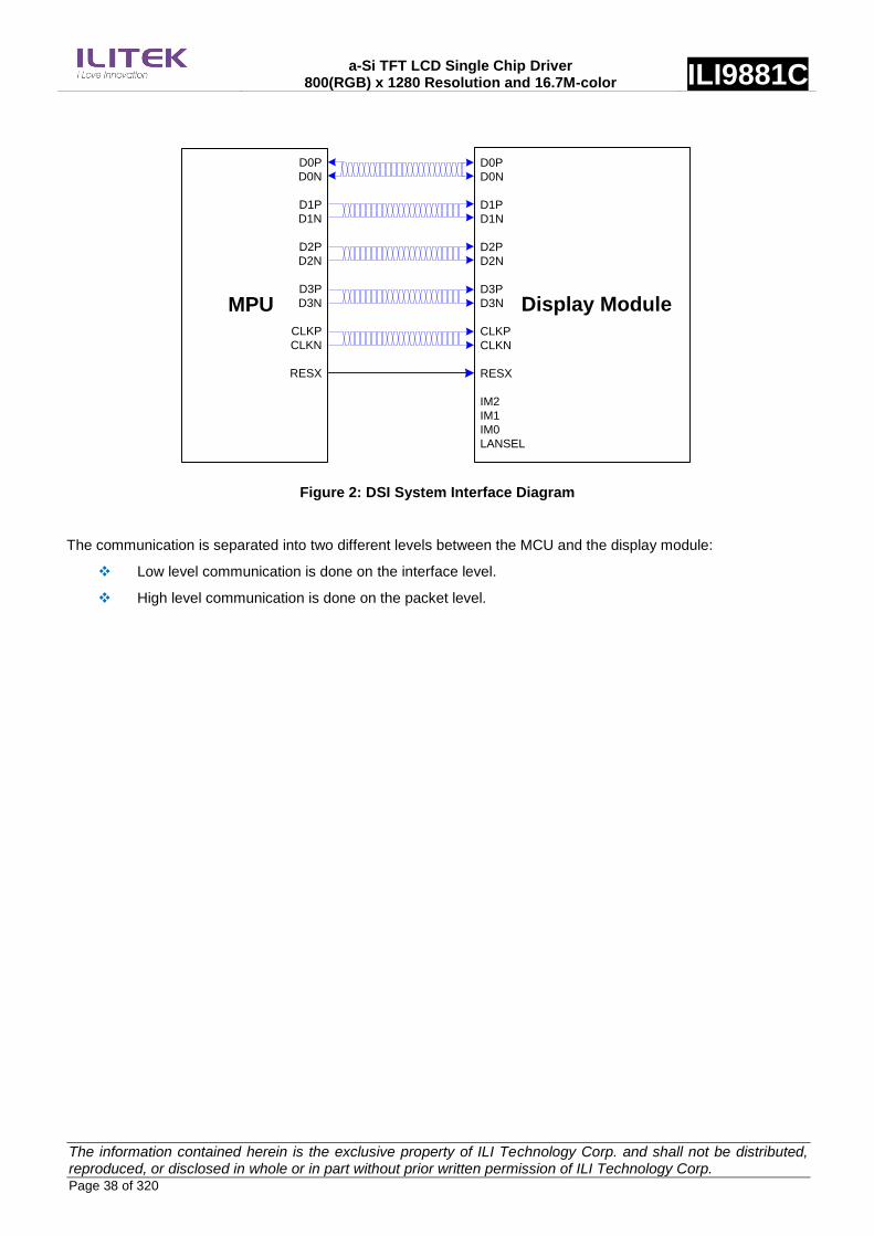
a-Si TFT LCD Single Chip Driver 800(RGB) x 1280 Resolution and 16.7M-color ILI9881C
The information contained herein is the exclusive property of ILI Technology Corp. and shall not be distributed, reproduced, or disclosed in whole or in part without prior written permission of ILI Technology Corp. Page 38 of 320
MPU Display Module
D0P
D0N
D1P
D1N
D2P
D2N
D3P
D3N
CLKP
CLKN
RESX
IM2
IM1
IM0
LANSEL
D0P
D0N
D1P
D1N
D2P
D2N
D3P
D3N
CLKP
CLKN
RESX
Figure 2: DSI System Interface Diagram
The communication is separated into two different levels between the MCU and the display module:
Low level communication is done on the interface level.
High level communication is done on the packet level.

a-Si TFT LCD Single Chip Driver 800(RGB) x 1280 Resolution and 16.7M-color ILI9881C
The information contained herein is the exclusive property of ILI Technology Corp. and shall not be distributed, reproduced, or disclosed in whole or in part without prior written permission of ILI Technology Corp. Page 39 of 320
4.1.2. Interface Level Communication
4.1.2.1. General
The display module uses data and clock lane differential pairs for DSI (DSI-2M). Both differential lane pairs can be
driven to Low Power (LP) or High Speed (HS) mode.
Low Power mode means that each line of the differential pair is used in the single ended mode, a differential
receiver is disable (a termination resistor of the receiver is disable), and it can be driven into a low power mode.
High Speed mode means that differential pairs (the termination resistor of the receiver is enable) are not used in
the single ended mode.
Different modes and protocols are used in each mode when transferring information from the MCU to the display
module and vice versa.
The State Codes of the High Speed (HS) and Low Power (LP) lane pair are defined below.
Table 3: High Speed and Low-Power Lane Pair State Codes
Lane Pair State Code Line DC Voltage Levels High Speed (HS) Low Power
DATA_P DATA_N Burst Mode Control Mode Escape Mode
HS-0 Low (HS) High (HS) Differential – 0 Note 1 Note1
HS-1 High (HS) Low (HS) Differential – 1 Note 1 Note 1
LP-00 Low (LP) Low (LP) Not Defined Bridge Space
LP-01 Low (LP) High (LP) Not Defined HS – Request Mark - 0
LP-10 High (LP) Low (LP) Not Defined LP - Request Mark - 1
LP-11 High (LP) High (LP) Not Defined Stop Note 2
Notes:
1. Low-Power Receivers (LP-Rx) of the lane pair will check the LP-00 state code when the Lane Pair is in the
High Speed (HS) mode.
2. If Low-Power Receivers (LP-Rx) of the lane pair recognizes the LP-11 state code, then the lane pair will return
to LP-11 of the Control Mode.
3. n = 0, 1, 2 and 3 (D1P/N, D2 P/N and D3 P/N lanes only for HS-0 and HS-1)

a-Si TFT LCD Single Chip Driver 800(RGB) x 1280 Resolution and 16.7M-color ILI9881C
The information contained herein is the exclusive property of ILI Technology Corp. and shall not be distributed, reproduced, or disclosed in whole or in part without prior written permission of ILI Technology Corp. Page 40 of 320
4.1.2.2. DSI CLK Lanes
CLKP/N lanes can be driven into three different power modes: Low Power Mode (LPM), Ultra-Low Power Mode
(ULPM) and High Speed Clock Mode (HSCM). Clock lane are in the single ended mode (LP = Low Power) when
entering or leaving Low Power Mode (LPM) or Ultra-Low Power Mode (ULPM). Clock lane is in the single ended
mode (LP = Low Power) when entering in or leaving High Speed Clock Mode (HSCM).These entering and leaving
protocols use Clock lane in the single ended mode to generate an entering or leaving sequence. The principal flow
chart of the different Clock lane power modes is illustrated below.
LP-01LPM
LP-11
LP-10LP-00
LP-10
LP-00
ULPM
LP-00HS-0HS-0
HS-0HS-1
HSCM (HS Clocking)
SW Reset
HW Reset
Power ON Sequence
Figure 3: Clock lane Power Modes
4.1.2.2.1. Low Power Mode (LPM)
CLKP/N lanes can be driven to the Low Power Mode (LPM), when CLKP/N lanes enter LP-11 State Code, in three
different ways:
1) After SW Reset, HW Reset or Power On Sequence => LP-11
2) After CLKP/N lanes leave Ultra-Low Power Mode (ULPM, LP-00 State Code) => LP-10 => LP-11 (LPM).
This sequence is illustrated below.
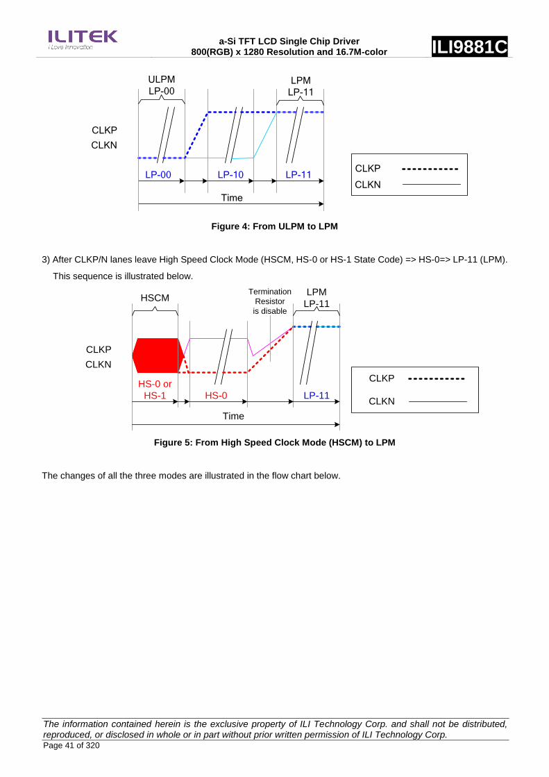
a-Si TFT LCD Single Chip Driver 800(RGB) x 1280 Resolution and 16.7M-color ILI9881C
The information contained herein is the exclusive property of ILI Technology Corp. and shall not be distributed, reproduced, or disclosed in whole or in part without prior written permission of ILI Technology Corp. Page 41 of 320
LP-00 LP-10 LP-11
Time
ULPM
LP-00LPM
LP-11
CLKP
CLKN
CLKP
CLKN
Figure 4: From ULPM to LPM
3) After CLKP/N lanes leave High Speed Clock Mode (HSCM, HS-0 or HS-1 State Code) => HS-0=> LP-11 (LPM).
This sequence is illustrated below.
HS-0 or
HS-1 HS-0 LP-11
Time
HSCMLPM
LP-11
Termination
Resistor
is disable
CLKP
CLKN
CLKP
CLKN
Figure 5: From High Speed Clock Mode (HSCM) to LPM
The changes of all the three modes are illustrated in the flow chart below.

a-Si TFT LCD Single Chip Driver 800(RGB) x 1280 Resolution and 16.7M-color ILI9881C
The information contained herein is the exclusive property of ILI Technology Corp. and shall not be distributed, reproduced, or disclosed in whole or in part without prior written permission of ILI Technology Corp. Page 42 of 320
LP-01LPM
LP-11
LP-10LP-00
LP-10
LP-00
ULPM
LP-00HS-0HS-0
HS-0HS-1
HSCM (HS Clocking)
SW Reset
HW Reset
Power ON Sequence
Mode Change
Figure 6: All Three Mode Changes to LPM
4.1.2.2.2. Ultra-Low Power Mode (ULPM)
CLKP/N lanes can be driven to the Ultra-Low power Mode (ULPM) when CLK lanes enter the LP-00 State Code.
The only entering possibility is from the Low Power Mode (LPM, LP-11 State Code) => LP-10 => LP-00 (ULPM).
This sequence is illustrated below.
LP-11 LP-10 LP-00
Time
LPM
LP-11ULPM
LP-00
CLKP
CLKN CLKP
CLKN
Figure 7: From LPM to ULPM

a-Si TFT LCD Single Chip Driver 800(RGB) x 1280 Resolution and 16.7M-color ILI9881C
The information contained herein is the exclusive property of ILI Technology Corp. and shall not be distributed, reproduced, or disclosed in whole or in part without prior written permission of ILI Technology Corp. Page 43 of 320
The mode change is also illustrated below.
LP-01LPM
LP-11
LP-10LP-00
LP-10
LP-00
ULPM
LP-00HS-0HS-0
HS-0HS-1
HSCM (HS Clocking)
SW Reset
HW Reset
Power ON Sequence
Mode Change
Figure 8: Mode Change from LPM to ULPM
4.1.2.2.3. High-Speed Clock Mode (HSCM)
CLKP/N lanes can be driven to the High Speed Clock Mode (HSCM) when CLK lanes start to function between
HS-0 and HS-1 State Codes. The only entering possibility is from the Low Power Mode (LPM, LP-11 State Code)
=> LP-01 => LP-00 => HS-0 => HS-0/1 (HSCM). This sequence is illustrated below.
LP-11 LP-01 LP-00
Time
LPM
LP-11
CLKP
CLKN
Termination Resistor
is enable
CLKP
CLKN
HSCM
HS-0
HS-1
HS-0 HS-0/1
Figure 9: From LPM to HSCM

a-Si TFT LCD Single Chip Driver 800(RGB) x 1280 Resolution and 16.7M-color ILI9881C
The information contained herein is the exclusive property of ILI Technology Corp. and shall not be distributed, reproduced, or disclosed in whole or in part without prior written permission of ILI Technology Corp. Page 44 of 320
The mode change is also illustrated below.
LP-01LPM
LP-11
LP-10LP-00
LP-10
LP-00
ULPM
LP-00HS-0HS-0
HS-0HS-1
HSCM (HS Clocking)
SW Reset
HW Reset
Power ON Sequence
Mode Change
Figure 10: Mode Change from LPM to HSCM
The high speed clock (CLKP/N) starts before high speed data is sent via data lanes. The high speed clock
continues clocking after the high speed data sending is stopped.
The burst of the high speed clock consists of:
Even number of transitions
Start state is HS-0
End state is HS-0
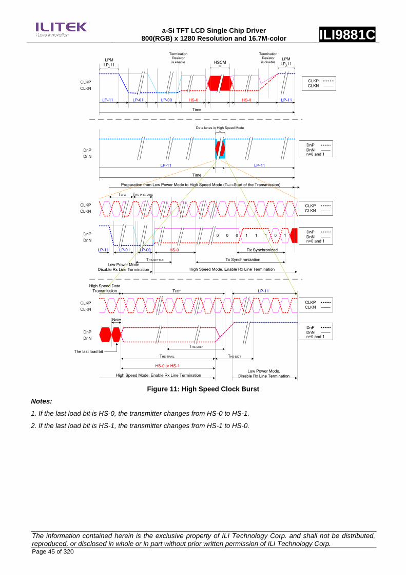
a-Si TFT LCD Single Chip Driver 800(RGB) x 1280 Resolution and 16.7M-color ILI9881C
The information contained herein is the exclusive property of ILI Technology Corp. and shall not be distributed, reproduced, or disclosed in whole or in part without prior written permission of ILI Technology Corp. Page 45 of 320
LP-11 LP-01 LP-00
Time
LPM
LP-11
CLKP
CLKN
HSCM
HS-0
LPM
LP-11
Termination
Resistor
is disable
Termination
Resistor
is enable
HS-0 LP-11
Time
LP-11 LP-11
Data lanes in High Speed Mode
TLPX THS-PREPARE
Preparation from Low Power Mode to High Speed Mode (TSOT=Start of the Transmission)
THS-SETTLE
Low Power Mode
Disable Rx Line Termination High Speed Mode, Enable Rx Line Termination
Tx Synchronization
Rx SynchronizedLP-11 LP-01 LP-00 HS-0
0 0 0 1 1 1 10
LP-11TEOT
High Speed Data
Transmission
THS-EXIT
THS-SKIP
THS-TRAIL
HS-0 or HS-1
High Speed Mode, Enable Rx Line TerminationLow Power Mode,
Disable Rx Line Termination
Note
DnP
DnN
CLKP
CLKN
DnP
DnN
CLKP
CLKN
DnP
DnN
The last load bit
CLKP
CLKN
CLKP
CLKN
CLKP
CLKN
DnP
DnNn=0 and 1
DnP
DnNn=0 and 1
DnP
DnNn=0 and 1
Figure 11: High Speed Clock Burst
Notes:
1. If the last load bit is HS-0, the transmitter changes from HS-0 to HS-1.
2. If the last load bit is HS-1, the transmitter changes from HS-1 to HS-0.

a-Si TFT LCD Single Chip Driver 800(RGB) x 1280 Resolution and 16.7M-color ILI9881C
The information contained herein is the exclusive property of ILI Technology Corp. and shall not be distributed, reproduced, or disclosed in whole or in part without prior written permission of ILI Technology Corp. Page 46 of 320
4.1.2.3. DSI Data Lanes
4.1.2.3.1. General
D3P/N, D2P/N, D1P/N and D0P/N Data Lanes can be driven into different modes:
Escape Mode (Only D0P/N data lane is used)
High-Speed Data Transmission (all data lanes are used)
Bus Turnaround Request (Only D0P/N data lane are used)
These modes and their entering codes are defined in the following table.
Table 4: Entering and Leaving Sequences
Mode Entering Mode Sequence Leaving Mode Sequence
Escape Mode1 LP-11 LP-10 LP-00 LP-01 LP-00 LP-00 LP-10 LP-11 (Mark-1)
High-Speed Data Transmission2 LP-11 LP-01 LP-00 HS-0 (HS-0 or HS-1 ) LP-11
Bus Turnaround Request3 LP-11 LP-10 LP-00 LP-10 LP-00 Hi-Z
4.1.2.3.2. Escape Modes
D0P/N data lanes can be used in different Escape Modes when data lanes are in the Low Power (LP) mode. These
Escape Modes are used to:
Send “Low-Power Data Transmission” (LPDT) from the MCU to the display module,
Drive data lanes to “Ultra-Low Power State” (ULPS),
Indicate “Remote Application Reset” (RAR), which can reset the display module,
Indicate “Acknowledge” (ACK), which is used to transmit a non-error event from the display module to the
MCU.
The basic sequence of the Escape Mode is as follows:
Start: LP-11
Escape Mode Entry (EME): LP-11 => LP-10 => LP-00 => LP-01 => LP-00
Escape Command (EC), which is coded, when one of the data lanes changes from low-to-high-to-low then
this changed data lane presents the value of the current data bit (D0P = 1, D0N= 0). When DSI-D0
changes from low-to-high-to-low, the receiver will latch a data bit, which value is logical 0. The receiver will
use this low-to-high-to-low transition as its internal clock.
A load if it is needed
Exit Escape (Mark-1) LP-00 => LP-10 => LP-11
End: LP-11

a-Si TFT LCD Single Chip Driver 800(RGB) x 1280 Resolution and 16.7M-color ILI9881C
The information contained herein is the exclusive property of ILI Technology Corp. and shall not be distributed, reproduced, or disclosed in whole or in part without prior written permission of ILI Technology Corp. Page 47 of 320
This basic construction is illustrated below:
LP-11LP-10LP-00LP-00LP-00 LP-01LP-10LP-11
Time
Escape Mode Entry (EME)Escape
Command
Load If
Needed Mark-1
D0P
D0N
D0P
D0N
Figure 12 General Escape Mode Sequence
A total of eight Escape Commands (EC) are divided into two types: Mode and Trigger, as shown in Table 5:
Escape Commands.
An example of the Mode type Escape Command is „Ultra-Low Power Mode‟, where the MCU instructs the display
module to enter its Ultra-Low Power Mode.
Escape commands are defined in the following table.
Table 5: Escape Commands
Escape command Command Type Mode/Trigger Entry command Pattern
(First Bit Last Bit Transmitted) Dn D0
Low-Power Data Transmission Mode 1110 0001 b - X
Ultra-Low Power Mode Mode 0001 1110 b X X
Undefined-1, Note 1
Mode 1001 1111 b - -
Undefined-2, Note 1
Mode 1101 1110 b - -
Remote Application Reset Trigger 0110 0010 b - X
Acknowledge Trigger 0010 0001 b - X
Unknown-5, Note 1
Trigger 1010 0000 b - -
Notes:
1. This Escape command support is not implemented on the display module.
2. n = 1
3. x = Supported
4. - = Not Supported

a-Si TFT LCD Single Chip Driver 800(RGB) x 1280 Resolution and 16.7M-color ILI9881C
The information contained herein is the exclusive property of ILI Technology Corp. and shall not be distributed, reproduced, or disclosed in whole or in part without prior written permission of ILI Technology Corp. Page 48 of 320
4.1.2.3.2.1. Low-Power Data Transmission (LPDT)
The MCU can send data to the display module in the Low-Power Data Transmission (LPDT) mode when data
lanes enter the Escape Mode and Low-Power Data Transmission (LPDT) command is sent to the display module.
The display module also uses the same sequence when it sends data to the MCU. The Low Power Data
Transmission (LPDT) uses the following sequence:
Start: LP-11
Escape Mode Entry (EME): LP-11 => LP-10 => LP-00 => LP-01 => LP-00
Low-Power Data Transmission (LPDT) command in the Escape Mode: 1110 0001 (first to last bit)
Load (Data):
One or more bytes (one byte = 8 bit)
Data lanes are in pause mode when data lanes are stopped (both lanes are low) between bytes
Mark-1: LP-00 => LP-10 => LP-11
End: LP-11
This sequence is illustrated for reference purposes below:
LP-10
Escape Mode Entry (EME)
LP-11 LP-00 LP-00LP-01
Mark-1
LP-00 LP-10 LP-11
LP-11 1 1 1 0 0 0 10 1 LP-11
Low Power Data Transmission (LPDT)
Escape Mode
Entry (EME) Load (Data) Mark-1
NoteTime
D0P
D0ND0P
D0N
Figure 13: Low-Power Data Transmission (LPDT)
Note: Load (Data) presents that the first bit is the logical 1 in this example.
Load Byte n Pause Load Byte n+1
1 11 1
Load (Data)
Time
D0P
D0N
D0P
D0N
Figure 14: Pause (Example)
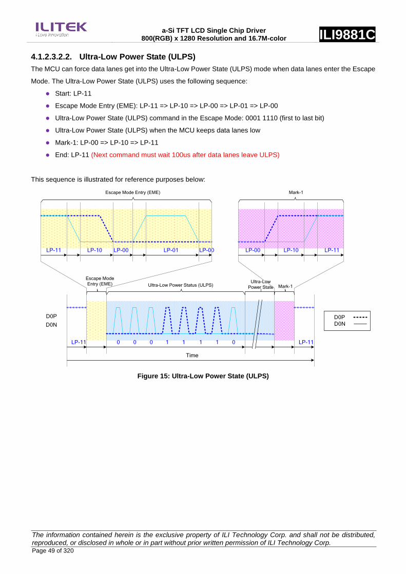
a-Si TFT LCD Single Chip Driver 800(RGB) x 1280 Resolution and 16.7M-color ILI9881C
The information contained herein is the exclusive property of ILI Technology Corp. and shall not be distributed, reproduced, or disclosed in whole or in part without prior written permission of ILI Technology Corp. Page 49 of 320
4.1.2.3.2.2. Ultra-Low Power State (ULPS)
The MCU can force data lanes get into the Ultra-Low Power State (ULPS) mode when data lanes enter the Escape
Mode. The Ultra-Low Power State (ULPS) uses the following sequence:
Start: LP-11
Escape Mode Entry (EME): LP-11 => LP-10 => LP-00 => LP-01 => LP-00
Ultra-Low Power State (ULPS) command in the Escape Mode: 0001 1110 (first to last bit)
Ultra-Low Power State (ULPS) when the MCU keeps data lanes low
Mark-1: LP-00 => LP-10 => LP-11
End: LP-11 (Next command must wait 100us after data lanes leave ULPS)
This sequence is illustrated for reference purposes below:
Escape Mode Entry (EME)
LP-11 LP-10 LP-00 LP-00LP-01
Mark-1
LP-00 LP-10 LP-11
LP-11 1 11000 01 LP-11
Ultra-Low Power Status (ULPS)
Escape Mode
Entry (EME)Ultra-Low
Power State Mark-1
Time
D0P
D0N
D0P
D0N
Figure 15: Ultra-Low Power State (ULPS)

a-Si TFT LCD Single Chip Driver 800(RGB) x 1280 Resolution and 16.7M-color ILI9881C
The information contained herein is the exclusive property of ILI Technology Corp. and shall not be distributed, reproduced, or disclosed in whole or in part without prior written permission of ILI Technology Corp. Page 50 of 320
4.1.2.3.2.3. Remote Application Reset (RAR)
The MCU can inform the display module that it should be reset in Remote Application Reset (RAR) trigger when
data lanes enter the Escape Mode. The Remote Application Reset (RAR) uses the following sequence:
Start: LP-11
Escape Mode Entry (EME): LP-11 => LP-10 => LP-00 => LP-01 => LP-00
Remote Application Reset (RAR) command in Escape Mode: 0110 0010 (first to last bit)
Mark-1: LP-00 => LP-10 => LP-11
End: LP-11
This sequence is illustrated for reference purposes below:
Escape Mode Entry (EME)
LP-11 LP-10 LP-00 LP-00LP-01
Mark-1
LP-00 LP-10 LP-11
LP-11 11 000 01 LP-11
Remote Application Reset (RAR)
Escape Mode
Entry (EME)Mark-1
Time
D0P
D0N
D0P
D0N
0
Figure 16: Remote Application Reset (RAR)
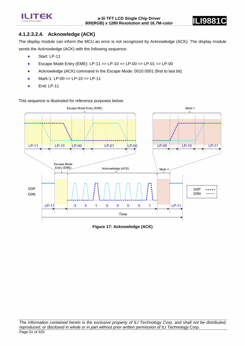
a-Si TFT LCD Single Chip Driver 800(RGB) x 1280 Resolution and 16.7M-color ILI9881C
The information contained herein is the exclusive property of ILI Technology Corp. and shall not be distributed, reproduced, or disclosed in whole or in part without prior written permission of ILI Technology Corp. Page 51 of 320
4.1.2.3.2.4. Acknowledge (ACK)
The display module can inform the MCU an error is not recognized by Acknowledge (ACK). The display module
sends the Acknowledge (ACK) with the following sequence:
Start: LP-11
Escape Mode Entry (EME): LP-11 => LP-10 => LP-00 => LP-01 => LP-00
Acknowledge (ACK) command in the Escape Mode: 0010 0001 (first to last bit)
Mark-1: LP-00 => LP-10 => LP-11
End: LP-11
This sequence is illustrated for reference purposes below:
Escape Mode Entry (EME)
LP-11 LP-10 LP-00 LP-00LP-01
Mark-1
LP-00 LP-10 LP-11
LP-11 10 000 10 LP-11
Acknowledge (ACK)
Escape Mode
Entry (EME)Mark-1
Time
D0P
D0N
D0P
D0N
0
Figure 17: Acknowledge (ACK)

a-Si TFT LCD Single Chip Driver 800(RGB) x 1280 Resolution and 16.7M-color ILI9881C
The information contained herein is the exclusive property of ILI Technology Corp. and shall not be distributed, reproduced, or disclosed in whole or in part without prior written permission of ILI Technology Corp. Page 52 of 320
4.1.2.3.3. High-Speed Data Transmission (HSDT)
4.1.2.3.3.1. Entering High-Speed Data Transmission (TSOT of HSDT)
The display module enters High-Speed Data Transmission (HSDT) when Clock lane CLKP/N have already entered
the High-Speed Clock Mode (HSCM) by the MCU. See more information in the section “4.1.2.2.3 High-Speed
Clock Mode (HSCM)”.
Data lanes D3P/N, D2P/N, D1P/N and D0P/N of the display module enter the High-Speed Data Transmission
(TSOT of HSDT) as follows:
Start: LP-11
HS-Request: LP-01
HS-Settle: LP-00 => HS-0 (Rx: Lane Termination Enable)
Rx Synchronization: 011101 (Tx (= MCU) Synchronization: 0001 1101)
End: High-Speed Data Transmission (HSDT) – Ready to receive High-Speed Data Load
The sequence of entering High-Speed Data Transmission (TSOT of HSDT) is illustrated below:
TLPX THS-PREPARE
Preparation from Low Power Mode to High Speed Mode (TSOT=Start of the Transmission)
THS-SETTLE
Low Power Mode
Disable Rx Line Termination High Speed Mode, Enable Rx Line Termination
Tx Synchronization
Rx SynchronizedLP-11 LP-01 LP-00 HS-0
0 0 0 1 1 1 10
CLKP
CLKN
DnP
DnN
CLKP
CLKN
DnP
DnN
HSDT
n=0 and 1
Figure 18: Entering High-Speed Data Transmission (TSOT of HSDT)

a-Si TFT LCD Single Chip Driver 800(RGB) x 1280 Resolution and 16.7M-color ILI9881C
The information contained herein is the exclusive property of ILI Technology Corp. and shall not be distributed, reproduced, or disclosed in whole or in part without prior written permission of ILI Technology Corp. Page 53 of 320
4.1.2.3.3.2. Leaving High-Speed Data Transmission (TEOT of HSDT)
The display module leaves the High-Speed Data Transmission (TEOT of HSDT) when Clock lane DSICLK+/- are in
the High-Speed Clock Mode (HSCM) by the MCU, and this HSCM is kept until data lanes D3P/N, D2P/N, D1P/N
and D0P/N are in the LP-11 mode. See more information in the section “4.1.2.2.3 High-Speed Clock Mode
(HSCM)”. Data lanes D3P/N, D2P/N, D1P/N and D0P/N of the display module leave the High-Speed Data
Transmission (TEOT of HSDT) as follows:
Start: High-Speed Data Transmission (HSDT)
Stops High-Speed Data Transmission
MCU changes to HS-1, if the last load bit is HS-0
MCU changes to HS-0, if the last load bit is HS-1
End: LP-11 (Rx: Lane Termination Disable)
The sequence of leaving High-Speed Data Transmission (TEOT of HSDT) is illustrated below:
LP-11TEOT
High Speed Data
Transmission
THS-EXIT
THS-SKIP
THS-TRAIL
HS-0 or HS-1
High Speed Mode, Enable Rx Line TerminationLow Power Mode,
Disable Rx Line Termination
Note
CLKP
CLKN
DnP
DnN
The last load bit
CLKP
CLKN
DnP
DnN
n=0 and 1
Figure 19: Leaving High-Speed Data Transmission (TEOT of HSDT)
Notes:
1. If the last load bit is HS-0, the transmitter changes from HS-0 to HS-1.
2. If the last load bit is HS-1, the transmitter changes from HS-1 to HS-0.

a-Si TFT LCD Single Chip Driver 800(RGB) x 1280 Resolution and 16.7M-color ILI9881C
The information contained herein is the exclusive property of ILI Technology Corp. and shall not be distributed, reproduced, or disclosed in whole or in part without prior written permission of ILI Technology Corp. Page 54 of 320
4.1.2.3.3.3. Burst of the High-Speed Data Transmission (HSDT)
The burst of the “High-Speed Data Transmission” (HSDT) can consist of one or several data packet(s). These data
packets can be Long (LPa) or Short (SPa) packets. These packets are defined in the section “4.1.3.1 Short Packet
(SPa) and Long Packet (LPa) Structures”. These different burst of the High-Speed Data Transmission (HSDT)
cases are illustrated for reference purposes below.
LP-11 SOTLPa
(Long Packet)EOT LP-11
LP-11 SOT EOT LP-11SPa
(Short Packet)
DnP/N n=0 and 1
DnP/N n=0 and 1
Figure 20: Single Packet in High-Speed Data Transmissions
The multiple packets in High-Speed Data Transmission are illustrated for reference purposes below:
DnP/N n=0 and 1
DnP/N n=0 and 1
LP-11 LP-11
LP-11 LP-11
SOTLPa
(Long Packet)
SPa
(Short Packet)EOT
SOT EOTSPa
(Short Packet)
SPa
(Short Packet)
SPa
(Short Packet)
Figure 21: Multiple Packets in High-Speed Data Transmission – Examples
Table 6: Abbreviations
Abbreviation Explanation
EOT End of the Transmission
LPa Long Packet
LP-11 Low Power Mode, Both of Data lanes are „1‟s (Stop Mode)
SPa Short Packet
SOT Start of the Transmission
Byte orders of the sent packet in High-Speed Data Transmission (HSDT) are as follows.
LP-11 LP-11SOTD1P/N EOTByte 5 Byte N-2
LP-11 LP-11SOT Byte 0D0P/N
EOTByte 4 Byte N-3
Byte 1
LP-11 LP-11SOTD3P/N EOTByte 3 Byte N
LP-11 LP-11SOTD2P/N
EOTByte 2 Byte N-1Byte 6
Byte 7
Figure 22: Number of Bytes, N, transmitted is an integer multiple of the number of lanes

a-Si TFT LCD Single Chip Driver 800(RGB) x 1280 Resolution and 16.7M-color ILI9881C
The information contained herein is the exclusive property of ILI Technology Corp. and shall not be distributed, reproduced, or disclosed in whole or in part without prior written permission of ILI Technology Corp. Page 55 of 320
LP-11 SOTD1P/N Byte 5
LP-11 LP-11SOT Byte 0D0P/N
EOTByte 4 Byte N
Byte 1
LP-11 LP-11SOTD3P/N Byte 3
LP-11 SOTD2P/N
Byte 2 Byte 6
Byte 7 EOT
LP-11EOT
LP-11EOT
Figure 23: Number of Bytes, N, transmitted is NOT an integer multiple of the number of lanes (Example 1)
LP-11 LP-11SOTD1P/N EOTByte 5 Byte N
LP-11 LP-11SOT Byte 0D0P/N
EOTByte 4 Byte N-1
Byte 1
LP-11 LP-11SOTD3P/N Byte 3
LP-11 SOTD2P/N
Byte 2 Byte 6
Byte 7 EOT
LP-11EOT
Figure 24: Number of Bytes, N, transmitted is NOT an integer multiple of the number of lanes (Example 2)
LP-11 LP-11SOTD1P/N EOTByte 5 Byte N-1
LP-11 LP-11SOT Byte 0D0P/N
EOTByte 4 Byte N-2
Byte 1
LP-11 LP-11SOTD3P/N Byte 3
LP-11 LP-11SOTD2P/N
EOTByte 2 Byte NByte 6
Byte 7 EOT
Figure 25: Number of Bytes, N, transmitted is NOT an integer multiple of the number of lanes (Example 3)

a-Si TFT LCD Single Chip Driver 800(RGB) x 1280 Resolution and 16.7M-color ILI9881C
The information contained herein is the exclusive property of ILI Technology Corp. and shall not be distributed, reproduced, or disclosed in whole or in part without prior written permission of ILI Technology Corp. Page 56 of 320
Byte 1
Byte 0
n-1 Packet n Packet
Byte N-3
Byte N-2
D0P/N
D1P/N
Byte 2Byte N-1
Byte 3Byte N
D2P/N
D3P/N
Figure 26: Continuous Multiple Packets in HSDT when Number of Bytes is Equal on Data Lanes at the End
of the Packet
Byte 0
Byte N
n-1 Packet n Packet
Byte N-4
Byte N-3
D0P/N
D1P/N
Byte 1Byte N-2
Byte 2Byte N-1
D2P/N
D3P/N
Figure 27: Continuous Multiple Packets in HSDT when Number of Bytes is not Equal on Data Lanes at the
End of the Packet (Example 1)
Byte N
Byte N-1
n-1 Packet n Packet
Byte N-5
Byte N-4
D0P/N
D1P/N
Byte 0Byte N-3
Byte 1Byte N-2
D2P/N
D3P/N
Figure 28: Continuous Multiple Packets in HSDT when Number of Bytes is not Equal on Data Lanes at the
End of the Packet (Example 2)

a-Si TFT LCD Single Chip Driver 800(RGB) x 1280 Resolution and 16.7M-color ILI9881C
The information contained herein is the exclusive property of ILI Technology Corp. and shall not be distributed, reproduced, or disclosed in whole or in part without prior written permission of ILI Technology Corp. Page 57 of 320
Byte N-1
Byte N-2
n-1 Packet n Packet
Byte N-6
Byte N-5
D0P/N
D1P/N
Byte NByte N-4
Byte 0Byte N-3
D2P/N
D3P/N
Figure 29: Continuous Multiple Packets in HSDT when Number of Bytes is not Equal on Data Lanes at the
End of the Packet (Example 3)

a-Si TFT LCD Single Chip Driver 800(RGB) x 1280 Resolution and 16.7M-color ILI9881C
The information contained herein is the exclusive property of ILI Technology Corp. and shall not be distributed, reproduced, or disclosed in whole or in part without prior written permission of ILI Technology Corp. Page 58 of 320
4.1.2.3.4. Bus Turnaround (BTA)
The MCU or display module, which controls D0P/N Data Lanes, can start a bus turnaround procedure when it
requires information from a receiver, which can be the MCU or display module.
The MCU and display module use the same sequence when this bus turnaround procedure is used. The sequence,
when the MCU wants to do the bus turnaround procedure to the display module, is described for reference
purposes as follows:
Start (MCU): LP-11
Turnaround Request (MCU): LP-11 => LP-10 => LP-00 => LP-10 => LP-00
The MCU waits until the display module starts to control D0P/N data lanes and the MCU stops to control
D0P/N data lanes (= High-Z)
The display module changes to the stop mode: LP-00 => LP-10 => LP-11
The bus turnaround procedure (from the MCU to the display module) is illustrated below:
LP-11 LP-10 LP-00 LP-10 LP-00 LP-00 LP-10 LP-11
D0P
D0N
Turnaround Request (TAR)
LP-00
MCU Controls Data Lanes The MCU waits until the Display
Module starts to control data lanes
(its output drivers) when MCU can
put output drivers in the high-Z mode LP-Requests
Display Module Controls
Data Lanes
Bus Turnaround (BTA)
Time
D0P
D0N
Figure 30: Bus Turnaround Procedure
MCU and display module terms can be switched in Figure 30 if the Bus Turnaround (BTA) is from the display
module to the MCU.

a-Si TFT LCD Single Chip Driver 800(RGB) x 1280 Resolution and 16.7M-color ILI9881C
The information contained herein is the exclusive property of ILI Technology Corp. and shall not be distributed, reproduced, or disclosed in whole or in part without prior written permission of ILI Technology Corp. Page 59 of 320
4.1.3. Packet Level Communication
4.1.3.1. Short Packet (SPa) and Long Packet (LPa) Structures
Short Packet (SPa) and Long Packet (LPa) are always used when data transmission is done in Low Power Data
Transmission (LPDT) or High-Speed Data Transmission (HSDT) modes. The lengths of the packets are:
Short Packet (SPa): 4 bytes
Long Packet (LPa): 6 to 65,541 bytes
The type (SPa or LPa) of the packet can be recognized from their package headers (PH).
LP-11 SoT DI Data 0 Data 1 ECC EoT LP-11
Time
Packet Data
Packet Header (PH)
LP-11 : Low Power - Stop State
SoT : Start of Transmission
DI : 8-bit, Data Identification
Data 0 / Data 1 : 8-bit, Packet Data
ECC : 8-bit, Error Correction Code
EoT : End of Transmission
Figure 31: Short Packet (SPa) Structure
LP-11 SoT DI WC ECC
EoT LP-11
Data 0 Data 1
CSData(WC-2) Data(WC-1)
Time
Time
LP-11 : Low Power - Stop State
SoT : Start of Transmission
DI : 8-bit, Data Identification
WC : 16-bit, Word Count
ECC : 8-bit, Error Correction Code
Data 0 ,…Data(WC-1) : Packet Data (0~65535 bytes)
CS : 16-bit, Check Sum = Packet Footer (PF)
EoT : End of Transmission
Packet Header (PH)
Figure 32: Long Packet (LPa) Structure
Notes:
1. Figure 31 and Figure 32 present a single packet sending (= Includes LP-11, SoT and EoT for each packet
sending).
2. The other possibility is that SoT, EoT and LP-11 are not needed between packets if packets are sent in
multiple packet format, e.g.
LP-11 => SoT => SPa => LPa => SPa => SPa => EoT => LP-11
LP-11 => SoT => SPa => SPa => SPa => EoT => LP-11
LP-11 => SoT => LPa => LPa => LPa => EoT => LP-11

a-Si TFT LCD Single Chip Driver 800(RGB) x 1280 Resolution and 16.7M-color ILI9881C
The information contained herein is the exclusive property of ILI Technology Corp. and shall not be distributed, reproduced, or disclosed in whole or in part without prior written permission of ILI Technology Corp. Page 60 of 320
4.1.3.1.1. Bit Order of the Byte on Packets
The bit order of the byte, what is used in packets, is that the Least Significant Bit (LSB) of the byte is sent first, and
the Most Significant Bit (MSB) is sent last. The order is illustrated for reference purposes below.
DI (Data Identification)
B
0
B
1
B
2
B
3
B
4
B
5
B
7
B
6
WC - LSB(Word Count - LSB)
B
0
B
1
B
2
B
3
B
4
B
5
B
7
B
6
WC - MSB(Word Count - MSB)
B
0
B
1
B
2
B
3
B
4
B
5
B
7
B
6
B
0
B
1
B
2
B
3
B
4
B
5
B
7
B
6
ECC(Error Correction Code)
L
S
B
L
S
B
L
S
B
M
S
B
M
S
B
M
S
B
L
S
B
M
S
B
0 1
8'b 29h 8'b 01h 8'b 00h 8'b 06h
00 0 0 01 0 1 1 0 0 0 0 0 0 0 0 0 0 0 0 0 0 1 1 0 0 000
Time
Figure 33: Bit Order of the Byte on Packets
4.1.3.1.2. Byte Order of the Multiple Byte Information on Packets
Byte order of the multiple bytes information, what is used in packets, is that the Least Significant (LS) Byte of the
information is sent first and the Most Significant (MS) Byte is sent last. For example, Word Count (WC) consists of
2 bytes (= 16 bits); while the LS byte is sent first and the MS byte is sent last. The order is illustrated for reference
purposes below.
WC - LSB(Word Count – Least Significant Byte)
Bit 0 Bit 1 Bit 2 Bit 3 Bit 4 Bit 5 Bit 7Bit 6
WC - MSB(Word Count – Most Significant Byte)
Bit 0 Bit 1 Bit 2 Bit 3 Bit 4 Bit 5 Bit 7Bit 6
LSB LSBMSB MSB
8'b 01h 8'b 00h
01 0 0 0 0 0 0 0 0 0 0 0 0 00
Time
Figure 34: Byte Order of the Multiple Byte Information on Packets
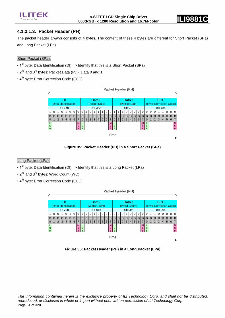
a-Si TFT LCD Single Chip Driver 800(RGB) x 1280 Resolution and 16.7M-color ILI9881C
The information contained herein is the exclusive property of ILI Technology Corp. and shall not be distributed, reproduced, or disclosed in whole or in part without prior written permission of ILI Technology Corp. Page 61 of 320
4.1.3.1.3. Packet Header (PH)
The packet header always consists of 4 bytes. The content of these 4 bytes are different for Short Packet (SPa)
and Long Packet (LPa).
Short Packet (SPa):
• 1st byte: Data Identification (DI) => Identify that this is a Short Packet (SPa)
• 2nd
and 3rd
bytes: Packet Data (PD), Data 0 and 1
• 4th byte: Error Correction Code (ECC)
DI (Data Identification)
B
0
B
1
B
2
B
3
B
4
B
5
B
7
B
6
Data 0(Packet Data)
B
0
B
1
B
2
B
3
B
4
B
5
B
7
B
6
Data 1(Packet Data)
B
0
B
1
B
2
B
3
B
4
B
5
B
7
B
6
B
0
B
1
B
2
B
3
B
4
B
5
B
7
B
6
ECC(Error Correction Code)
L
S
B
L
S
B
L
S
B
M
S
B
M
S
B
M
S
B
L
S
B
M
S
B
1 0
8'b 15h 8'b 3Ah 8'b 07h 8'b 18h
01 0 0 01 0 0 0 1 0 1 1 1 1 1 1 0 0 0 0 0 0 0 0 1 1 000
Time
Packet Header (PH)
Figure 35: Packet Header (PH) in a Short Packet (SPa)
Long Packet (LPa):
• 1st byte: Data Identification (DI) => Identify that this is a Long Packet (LPa)
• 2nd
and 3rd
bytes: Word Count (WC)
• 4th byte: Error Correction Code (ECC)
DI (Data Identification)
B
0
B
1
B
2
B
3
B
4
B
5
B
7
B
6
Data 0(Word Count)
B
0
B
1
B
2
B
3
B
4
B
5
B
7
B
6
Data 1(Word Count)
B
0
B
1
B
2
B
3
B
4
B
5
B
7
B
6
B
0
B
1
B
2
B
3
B
4
B
5
B
7
B
6
ECC(Error Correction Code)
L
S
B
L
S
B
L
S
B
M
S
B
M
S
B
M
S
B
L
S
B
M
S
B
0 1
8'b 29h 8'b 01h 8'b 00h 8'b 06h
00 0 0 01 0 1 0 0 0 1 0 0 0 0 0 1 0 0 0 0 0 1 1 0 0 000
Time
Packet Header (PH)
Figure 36: Packet Header (PH) in a Long Packet (LPa)

a-Si TFT LCD Single Chip Driver 800(RGB) x 1280 Resolution and 16.7M-color ILI9881C
The information contained herein is the exclusive property of ILI Technology Corp. and shall not be distributed, reproduced, or disclosed in whole or in part without prior written permission of ILI Technology Corp. Page 62 of 320
4.1.3.1.3.1. Data Identification (DI)
Data Identification (DI) is a part of the Packet Header (PH), and it consists of 2 parts:
Virtual Channel (VC), 2 bits, DI [7...6]
Data Type (DT), 6 bits, DI [5…0]
The Data Identification (DI) structure is illustrated, see the figure below.
DI (Data Identification)
Bit 7 Bit 6 Bit 5 Bit 4 Bit 3 Bit 2 Bit 0Bit 1
VC
(Virtual Channel Identifier)
DT
(Data Type)
Figure 37: Data Identification (DI) Structure
Data Identification (DI) in the Packet Header (PH) is illustrated for reference purposes below.
Packet Header (PH)
DI (Data Identification)
B
0
B
1
B
2
B
3
B
4
B
5
B
7
B
6
WC - LSB(Word Count - LSB)
B
0
B
1
B
2
B
3
B
4
B
5
B
7
B
6
WC - MSB(Word Count - MSB)
B
0
B
1
B
2
B
3
B
4
B
5
B
7
B
6
B
0
B
1
B
2
B
3
B
4
B
5
B
7
B
6
ECC(Error Correction Code)
L
S
B
L
S
B
L
S
B
M
S
B
M
S
B
M
S
B
L
S
B
M
S
B
0 1
8'b 29h 8'b 01h 8'b 00h 8'b 06h
00 0 0 01 0 1 1 0 0 0 0 0 0 0 0 0 0 0 0 0 0 1 1 0 0 000
Time
Figure 38: Data Identification (DI) on the Packet Header (PH)
4.1.3.1.3.1.1. Virtual Channel (VC)
Virtual Channel (VC) is a part of Data Identification (DI [7…6]) structure, and it is used to address where a packet is
to be sent from the MCU. Bits of the Virtual Channel (VC) are illustrated for reference purposes below.
Packet Header (PH)
DI (Data Identification)
B
0
B
1
B
2
B
3
B
4
B
5
B
7
B
6
WC - LSB(Word Count - LSB)
B
0
B
1
B
2
B
3
B
4
B
5
B
7
B
6
WC - MSB(Word Count - MSB)
B
0
B
1
B
2
B
3
B
4
B
5
B
7
B
6
B
0
B
1
B
2
B
3
B
4
B
5
B
7
B
6
ECC(Error Correction Code)
L
S
B
L
S
B
L
S
B
M
S
B
M
S
B
M
S
B
L
S
B
M
S
B
0 1
8'b 29h 8'b 01h 8'b 00h 8'b 06h
00 0 0 01 0 1 1 0 0 0 0 0 0 0 0 0 0 0 0 0 0 1 1 0 0 000
Time
Figure 39: Virtual Channel (VC) on the Packet Header (PH)
Virtual Channel (VC) can assign 4 different channels for 4 different display modules. Devices will use the same
virtual channel as which the MCU uses to send packets to them, e.g.

a-Si TFT LCD Single Chip Driver 800(RGB) x 1280 Resolution and 16.7M-color ILI9881C
The information contained herein is the exclusive property of ILI Technology Corp. and shall not be distributed, reproduced, or disclosed in whole or in part without prior written permission of ILI Technology Corp. Page 63 of 320
The MCU uses the virtual channel 0 when it sends packets to the ILI9881C
The ILI9881C also uses the virtual channel 0 when it sends packets to the MCU
This functionality is illustrated below.
MCU
Virtual
Channel
Selector
Long and
Short Packets
Display Module
DI[7:6]=VC[1:0]=2'b00b (ILI9881C)
DI[7:6]=VC[1:0]=2'b01b (Other Device 1)
DI[7:6]=VC[1:0]=2'b10b (Other Device 2)
DI[7:6]=VC[1:0]=2'b11b (Other Device 3)
Figure 40: Virtual Channel (VC) Configuration
Virtual Channel (VC) is always 0 (DI [7..6] = VC [1..0] = 00b) when the MCU sends “End of Transmission Packet” to
the display module. See the section “4.1.3.2.1.7 End of Transmission Packet (EoTP)”.
This display module does not support the virtual channel selector for other devices (1 to 3) when the only possible
virtual channel (VC [1..0]) is 00b for the ILI9881C.
4.1.3.1.3.1.2. Data Type (DT)
Data Type (DT) is a part of Data Identification (DI [5…0]) structure, and it is used to define the type of the used data
in a packet. Bits of the Data Type (DT) are illustrated for reference purposes below.
Packet Header (PH)
DI (Data Identification)
B
0
B
1
B
2
B
3
B
4
B
5
B
7
B
6
WC - LSB(Word Count - LSB)
B
0
B
1
B
2
B
3
B
4
B
5
B
7
B
6
WC - MSB(Word Count - MSB)
B
0
B
1
B
2
B
3
B
4
B
5
B
7
B
6
B
0
B
1
B
2
B
3
B
4
B
5
B
7
B
6
ECC(Error Correction Code)
L
S
B
L
S
B
L
S
B
M
S
B
M
S
B
M
S
B
L
S
B
M
S
B
0 1
8'b 29h 8'b 01h 8'b 00h 8'b 06h
00 0 0 01 0 1 1 0 0 0 0 0 0 0 0 0 0 0 0 0 0 1 1 0 0 000
Time
Figure 41: Data Type (DT) on the Packet Header (PH)
This Data Type (DT) also defines the used packet is a Short Packet (SPa) or a Long Packet (LPa). Data Types (DT)
are different from the MCU to the display module (or other devices) and vice versa. These Data Types (DT) are
defined in the tables below.

a-Si TFT LCD Single Chip Driver 800(RGB) x 1280 Resolution and 16.7M-color ILI9881C
The information contained herein is the exclusive property of ILI Technology Corp. and shall not be distributed, reproduced, or disclosed in whole or in part without prior written permission of ILI Technology Corp. Page 64 of 320
Table 7: Data Type (DT) from the MCU to the Display Module
From the MCU to the Display Module
Bit5 Bit4 Bit3 Bit2 Bit1 Bit0 Hex Description Short/Long Packet
0 0 0 0 0 1 01 Sync Event, V Sync Start SPa (Short Packet)
0 1 0 0 0 1 11 Sync Event, V Sync End SPa (Short Packet)
1 0 0 0 0 1 21 Sync Event, H Sync Start SPa (Short Packet)
1 1 0 0 0 1 31 Sync Event, H Sync End SPa (Short Packet)
0 0 1 0 0 0 08 End of Transmission Packet (EoTP) Note1
SPa (Short Packet)
0 0 0 0 1 0 02 Color Mode Off Command SPa (Short Packet)
0 1 0 0 1 0 12 Color Mode On Command SPa (Short Packet)
1 0 0 0 1 0 22 Shut Down Peripheral Command SPa (Short Packet)
1 1 0 0 1 0 32 Turn On Peripheral Command SPa (Short Packet)
0 0 0 0 1 1 03 Generic Short WRITE, no parameters SPa (Short Packet)
0 1 0 0 1 1 13 Generic Short WRITE, 1 parameters SPa (Short Packet)
1 0 0 0 1 1 23 Generic Short WRITE, 2 parameters SPa (Short Packet)
0 0 0 1 0 0 04 Generic Short READ, no parameters SPa (Short Packet)
0 1 0 1 0 0 14 Generic Short READ, 1 parameters SPa (Short Packet)
1 0 0 1 0 0 24 Generic Short READ, 2 parameters SPa (Short Packet)
0 0 0 1 0 1 05 DCS Write, No Parameter SPa (Short Packet)
0 1 0 1 0 1 15 DCS Write, 1 Parameter SPa (Short Packet)
0 0 0 1 1 0 06 DCS Read, No Parameter SPa (Short Packet)
1 1 0 1 1 1 37 Set Maximum Return Packet Size SPa (Short Packet)
0 0 1 0 0 1 09 Null Packet, No Data, Note2
LPa (Long Packet)
0 1 1 0 0 1 19 Blanking Packet, no data LPa (Long Packet)
1 0 1 0 0 1 29 Generic Long Write LPa (Long Packet)
1 1 1 0 0 1 39 DCS Write Long LPa (Long Packet)
0 0 1 1 1 0 0E Packed Pixel Stream, 16-bit RGB, 5-6-5 Format LPa (Long Packet)
0 1 1 1 1 0 1E Packed Pixel Stream, 18-bit RGB, 6-6-6 Format LPa (Long Packet)
1 0 1 1 1 0 2E Loosely Packed Pixel Stream, 18-bit RGB, 6-6-6 Format LPa (Long Packet)
1 1 1 1 1 0 3E Packed Pixel Stream, 24-bit RGB, 8-8-8 Format LPa (Long Packet)
x
x
x
x
0
1
0
1
0
1
0
1
x0
xF
DO NOT USE
All unspecified codes are reserved
Notes:
1. This can be used when the MCU wants to make sure that it is the end of the transmission in High Speed Data
Transferring (HSDT) mode.
2. This can be used when data lanes are to be kept in High Speed Data Transferring (HSDT) Mode.

a-Si TFT LCD Single Chip Driver 800(RGB) x 1280 Resolution and 16.7M-color ILI9881C
The information contained herein is the exclusive property of ILI Technology Corp. and shall not be distributed, reproduced, or disclosed in whole or in part without prior written permission of ILI Technology Corp. Page 65 of 320
Table 8: Data Type (DT) from the Display Module to the MCU
From the Display Module to the MCU
Bit5 Bit4 Bit3 Bit2 Bit1 Bit0 Hex Description Short/Long Packet
0 0 0 0 1 0 02 Acknowledge with Error Report SPa (Short Packet)
0 0 1 0 0 0 08 End of Transmission Packet (EoTP) SPa (Short Packet)
0 1 0 0 0 1 11 Generic Short READ Response, 1 byte returned SPa (Short Packet)
0 1 0 0 1 0 12 Generic Short READ Response, 2 byte returned SPa (Short Packet)
0 1 1 0 1 0 1A Generic Long READ Response LPa (Long Packet)
0 1 1 1 0 0 1C DCS Read Long Response LPa (Long Packet)
1 0 0 0 0 1 21 DCS Read Short Response, 1 byte returned SPa (Short Packet)
1 0 0 0 1 0 22 DCS Read Short Response, 2 byte returned SPa (Short Packet)
The receiver will ignore other Data Types (DT) if they are not defined in Table 7 and Table 8.
4.1.3.1.3.2. Packet Data (PD) in a Short Packet (SPa)
Packet Data (PD) of the Short Packet (SPa) is placed after Data Type (DT) of the Data Identification (DI) and
indicates a Short Packet (SPa) is to be sent. Packet Data (PD) of a Short Packet (SPa) consists of 2 data bytes:
Data 0 and Data 1. The sending order of the Packet Data (PD) is that Data 0 is sent first and the Data 1 is sent last.
Bits of Data 1 are set to 0 if the information length is 1 byte. Packet Data (PD) of a Short Packet (SPa), when the
length of the information is 1 or 2 bytes and Virtual Channel (VC) is 0, are illustrated for reference purposes below.
Packet Data (PD) information:
• Data 0: 26hex (Display Command Set (DCS) with 1 Parameter => DI (Data Type (DT)) = 15hex)
• Data 1: 01hex (DCS‟s parameter)
DI (Data Identification)
B
0
B
1
B
2
B
3
B
4
B
5
B
7
B
6
Data 0(Packet Data)
B
0
B
1
B
2
B
3
B
4
B
5
B
7
B
6
Data 1(Packet Data)
B
0
B
1
B
2
B
3
B
4
B
5
B
7
B
6
B
0
B
1
B
2
B
3
B
4
B
5
B
7
B
6
ECC(Error Correction Code)
L
S
B
L
S
B
L
S
B
M
S
B
M
S
B
M
S
B
L
S
B
M
S
B
1 0
8'b 15h 8'b 26h 8'b 01h 8'b 3Eh
01 0 1 01 0 0 0 1 1 0 0 1 1 0 0 0 0 0 0 0 0 1 1 1 1 000
Time
Packet Header (PH)
Figure 42: Packet Data (PD) for Short Packet (SPa), 2 Bytes Information
Packet Data (PD) information:
• Data 0: 10hex (DCS without parameter => DI (Data Type (DT)) = 05hex)
• Data 1: 00hex (Null)

a-Si TFT LCD Single Chip Driver 800(RGB) x 1280 Resolution and 16.7M-color ILI9881C
The information contained herein is the exclusive property of ILI Technology Corp. and shall not be distributed, reproduced, or disclosed in whole or in part without prior written permission of ILI Technology Corp. Page 66 of 320
DI (Data Identification)
B
0
B
1
B
2
B
3
B
4
B
5
B
7
B
6
Data 0(Packet Data)
B
0
B
1
B
2
B
3
B
4
B
5
B
7
B
6
Data 1(Packet Data)
B
0
B
1
B
2
B
3
B
4
B
5
B
7
B
6
B
0
B
1
B
2
B
3
B
4
B
5
B
7
B
6
ECC(Error Correction Code)
L
S
B
L
S
B
L
S
B
M
S
B
M
S
B
M
S
B
L
S
B
M
S
B
1 0
8'b 05h 8'b 10h 8'b 00h 8'b 2Ch
00 0 1 01 0 0 0 0 0 0 1 0 0 0 0 0 0 0 0 0 0 0 1 1 0 000
Time
Packet Header (PH)
Figure 43: Packet Data (PD) for Short Packet (SPa), 1 Byte Information

a-Si TFT LCD Single Chip Driver 800(RGB) x 1280 Resolution and 16.7M-color ILI9881C
The information contained herein is the exclusive property of ILI Technology Corp. and shall not be distributed, reproduced, or disclosed in whole or in part without prior written permission of ILI Technology Corp. Page 67 of 320
4.1.3.1.3.3. Word Count (WC) in a Long Packet (LPa)
Word Count (WC) of the Long Packet (LPa) is placed after Data Type (DT) of the Data Identification (DI) and
indicates that a Long Packet (LPa) is to be sent. Word Count (WC) indicates the amount of data bytes of the
Packet Data (PD) that is to be sent after the Packet Header (PH). The location of the Word Count (WC) in a Long
Packet is the same as which of the Packet Data (PD) in a Short Packet (SPa), as shown in Figure 45. Word Count
(WC) of the Long Packet (LPa) consists of 2 bytes. The sending order of these 2 bytes of the Word Count (WC) is
that the Least Significant (LS) Byte is sent first, and the Most Significant (MS) Byte is sent last. Word Count (WC) of
a Long Packet (LPa) is illustrated for reference purposes below.
Packet Header (PH)
DI (Data Identification)
B
0
B
1
B
2
B
3
B
4
B
5
B
7
B
6
WC - LSB(Word Count - LSB)
B
0
B
1
B
2
B
3
B
4
B
5
B
7
B
6
WC - MSB(Word Count - MSB)
B
0
B
1
B
2
B
3
B
4
B
5
B
7
B
6
B
0
B
1
B
2
B
3
B
4
B
5
B
7
B
6
ECC(Error Correction Code)
L
S
B
L
S
B
L
S
B
M
S
B
M
S
B
M
S
B
L
S
B
M
S
B
0 1
8'b 29h 8'b 01h 8'b 00h 8'b 06h
00 0 0 01 0 1 1 0 0 0 0 0 0 0 0 0 0 0 0 0 0 1 1 0 0 000
Time
Figure 44: Word Count (WC) in a Long Packet (LPa)
LP-11 SoT DI Data 0 Data 1 ECC EoT LP-11
Time
Packet Header (PH) LP-11 : Low Power - Stop State
SoT : Start of Transmission
DI : 8-bit, Data Identification
Data 0 / Data 1 : 8-bit, Packet Data
ECC : 8-bit, Error Correction Code
EoT : End of Transmission
Short Packet (SPa)
Packet Data
LP-11 SoT DI WC ECC
EoT LP-11Data 0 Data 1 CSData(WC-2) Data(WC-1)
Time
Time
LP-11 : Low Power - Stop State
SoT : Start of Transmission
DI : 8-bit, Data Identification
WC : 16-bit, Word Count
ECC : 8-bit, Error Correction Code
Data 0 ,…Data(WC-1) : Packet Data (0~65535 bytes)
CS : 16-bit, Check Sum = Packet Footer (PF)
EoT : End of Transmission
Packet Header (PH)Long Packet (LPa)
Packet Data
Figure 45: Packet Data in Short and Long Packets

a-Si TFT LCD Single Chip Driver 800(RGB) x 1280 Resolution and 16.7M-color ILI9881C
The information contained herein is the exclusive property of ILI Technology Corp. and shall not be distributed, reproduced, or disclosed in whole or in part without prior written permission of ILI Technology Corp. Page 68 of 320
4.1.3.1.3.4. Error Correction Code (ECC)
The Error Correction Code (ECC) is a part of Packet Header (PH) and its purpose is to identify an error or errors.
The ECC protects the following fields:
Short Packet (SPa): Data Identification (DI) byte (8 bits: D [0…7]), Packet Data (PD) bytes (16 bits: D
[8…23]) and ECC (8 bits: P [0…7])
Long Packet (LPa): Data Identification (DI) byte (8 bits: D [0…7]), Word Count (WC) bytes (16 bits: D
[8…23]) and ECC (8 bits: P [0…7])
D [23…0] and P [7…0] are illustrated for reference purposes below.
DI (Data Identification)
B
0
B
1
B
2
B
3
B
4
B
5
B
7
B
6
Data 0(Packet Data)
B
0
B
1
B
2
B
3
B
4
B
5
B
7
B
6
Data 1(Packet Data)
B
0
B
1
B
2
B
3
B
4
B
5
B
7
B
6
B
0
B
1
B
2
B
3
B
4
B
5
B
7
B
6
ECC(Error Correction Code)
L
S
B
L
S
B
L
S
B
M
S
B
M
S
B
M
S
B
L
S
B
M
S
B
1 0
8'b 05h 8'b 10h 8'b 00h 8'b 2Ch
00 0 1 01 0 0 0 0 0 0 1 0 0 0 0 0 0 0 0 0 0 0 1 1 0 000
Time
Packet Header (PH)
Figure 46: D [23…0] and P [7…0] in a Short Packet (SPa)
Packet Header (PH)
DI (Data Identification)
B
0
B
1
B
2
B
3
B
4
B
5
B
7
B
6
WC - LSB(Word Count - LSB)
B
0
B
1
B
2
B
3
B
4
B
5
B
7
B
6
WC - MSB(Word Count - MSB)
B
0
B
1
B
2
B
3
B
4
B
5
B
7
B
6
B
0
B
1
B
2
B
3
B
4
B
5
B
7
B
6
ECC(Error Correction Code)
L
S
B
L
S
B
L
S
B
M
S
B
M
S
B
M
S
B
L
S
B
M
S
B
0 1
8'b 29h 8'b 01h 8'b 00h 8'b 06h
00 0 0 01 0 1 1 0 0 0 0 0 0 0 0 0 0 0 0 0 0 1 1 0 0 000
Time
Figure 47: D [23…0] and P [7…0] in a Long Packet (LPa)
Error Correction Code (ECC) can recognize one or several error(s) and can only correct one-bit error. Bits (P
[7…0]) of the Error Correction Code (ECC) are defined, where the symbol „^‟ presents the XOR function (Pn is 1 if
there is odd number of 1, and Pn is 0 if there is even number of 1), as follows.
• P7 = 0
• P6 = 0
• P5 = D10^D11^D12^D13^D14^D15^D16^D17^D18^D19^D21^D22^D23
• P4 = D4^D5^D6^D7^D8^D9^D16^D17^D18^D19^D20^D22^D23
• P3 = D1^D2^D3^D7^D8^D9^D13^D14^D15^D19^D20^D21^D23
• P2 = D0^D2^D3^D5^D6^D9^D11^D12^D15^D18^D20^D21^D22
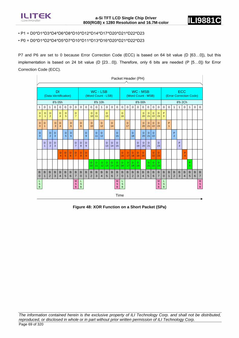
a-Si TFT LCD Single Chip Driver 800(RGB) x 1280 Resolution and 16.7M-color ILI9881C
The information contained herein is the exclusive property of ILI Technology Corp. and shall not be distributed, reproduced, or disclosed in whole or in part without prior written permission of ILI Technology Corp. Page 69 of 320
• P1 = D0^D1^D3^D4^D6^D8^D10^D12^D14^D17^D20^D21^D22^D23
• P0 = D0^D1^D2^D4^D5^D7^D10^D11^D13^D16^D20^D21^D22^D23
P7 and P6 are set to 0 because Error Correction Code (ECC) is based on 64 bit value (D [63…0]), but this
implementation is based on 24 bit value (D [23…0]). Therefore, only 6 bits are needed (P [5…0]) for Error
Correction Code (ECC).
Packet Header (PH)
DI (Data Identification)
WC - LSB(Word Count - LSB)
WC - MSB(Word Count - MSB)
ECC(Error Correction Code)
L
S
B
L
S
B
L
S
B
M
S
B
M
S
B
M
S
B
L
S
B
M
S
B
1 0
8'b 05h 8'b 10h 8'b 00h 8'b 2Ch
00 0 1 01 0 0 0 0 0 0 1 0 0 0 0 0 0 0 0 0 0 0 1 1 0 000
Time
D
0
D
10
D
1
D
2
D
4
D
5
D
7
D
11
D
13
D
16
D
20
D
21
D
22
D
23
P
0
D
0
D
10
D
3
D
1
D
4
D
6
D
8
D
12
D
14
D
17
D
20
D
21
D
22
D
23
P
1
D
0
D
12
D
3
D
2
D
6
D
5
D
9
D
11
D
15
D
18
D
20
D
21
D
22
P
2
D
1
D
13
D
3
D
2
D
8
D
7
D
9
D
14
D
15
D
19
D
20
D
21
D
23
P
3
D
4
D
16
D
6
D
5
D
8
D
7
D
9
D
17
D
18
D
19
D
22
D
20
D
23
P
4
D
12
D
16
D
11
D
10
D
14
D
13
D
15
D
17
D
18
D
19
D
22
D
21
D
23
P
5
B
0
B
1
B
2
B
3
B
4
B
5
B
7
B
6
B
0
B
1
B
2
B
3
B
4
B
5
B
7
B
6
B
0
B
1
B
2
B
3
B
4
B
5
B
7
B
6
B
0
B
1
B
2
B
3
B
4
B
5
B
7
B
6
Figure 48: XOR Function on a Short Packet (SPa)

a-Si TFT LCD Single Chip Driver 800(RGB) x 1280 Resolution and 16.7M-color ILI9881C
The information contained herein is the exclusive property of ILI Technology Corp. and shall not be distributed, reproduced, or disclosed in whole or in part without prior written permission of ILI Technology Corp. Page 70 of 320
Packet Header (PH)
DI (Data Identification)
WC - LSB(Word Count - LSB)
WC - MSB(Word Count - MSB)
ECC(Error Correction Code)
L
S
B
L
S
B
L
S
B
M
S
B
M
S
B
M
S
B
L
S
B
M
S
B
0 18'b 29h 8'b 01h 8'b 00h 8'b 06h
00 0 0 01 0 1 1 0 0 0 0 0 0 0 0 0 0 0 0 0 0 1 1 0 0 000
Time
D
0
D
10
D
1
D
2
D
4
D
5
D
7
D
11
D
13
D
16
D
20
D
21
D
22
D
23
P
0
D
0
D
10
D
3
D
1
D
4
D
6
D
8
D
12
D
14
D
17
D
20
D
21
D
22
D
23
P
1
D
0
D
12
D
3
D
2
D
6
D
5
D
9
D
11
D
15
D
18
D
20
D
21
D
22
P
2
D
1
D
13
D
3
D
2
D
8
D
7
D
9
D
14
D
15
D
19
D
20
D
21
D
23
P
3
D
4
D
16
D
6
D
5
D
8
D
7
D
9
D
17
D
18
D
19
D
22
D
20
D
23
P
4
D
12
D
16
D
11
D
10
D
14
D
13
D
15
D
17
D
18
D
19
D
22
D
21
D
23
P
5
B
0
B
1
B
2
B
3
B
4
B
5
B
7
B
6
B
0
B
1
B
2
B
3
B
4
B
5
B
7
B
6
B
0
B
1
B
2
B
3
B
4
B
5
B
7
B
6
B
0
B
1
B
2
B
3
B
4
B
5
B
7
B
6
Figure 49: XOR Function on a Long Packet (LPa)
The transmitter (= the MCU or the Display Module) will send data bits D [23…0] and Error Correction Code (ECC)
P [7…0]. The receiver (= the Display module or the MCU) will calculate the Internal Error Correction Code (IECC)
and compare the received Error Correction Code (ECC) and the Internal Error Correction Code (IECC). This
comparison is done when each power bit of ECC and IECC have performed the XOR function. The result of this
function is PO [7…0]. This functionality, where the transmitter is the MCU and the receiver is the display module, is
illustrated for reference purposes below.
Data: D[23:0]
ECC: P[0:7]
DSI I/F
Interface ECC (IECC)
Generator PI[0:7]
XOR
XOR
PI7
P7
PI0
P0
PO7
PO0
Display ModuleMCU
Figure 50: Internal Error Correction Code (IECC) on the Display Module (= the Receiver)
The sent data bits (D [23…0]) and ECC (P [7…0]) are correctly received if the value of the PO [7…0]) is 00h.
The sent data bits (D [23…0]) and ECC (P [7…0]) are not correctly received if the value of the PO [7…0]) is not
00h.
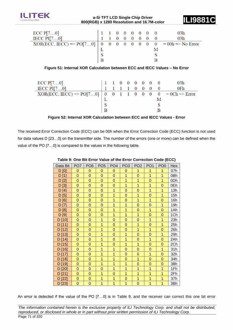
a-Si TFT LCD Single Chip Driver 800(RGB) x 1280 Resolution and 16.7M-color ILI9881C
The information contained herein is the exclusive property of ILI Technology Corp. and shall not be distributed, reproduced, or disclosed in whole or in part without prior written permission of ILI Technology Corp. Page 71 of 320
Figure 51: Internal XOR Calculation between ECC and IECC Values – No Error
Figure 52: Internal XOR Calculation between ECC and IECC Values - Error
The received Error Correction Code (ECC) can be 00h when the Error Correction Code (ECC) function is not used
for data values D [23…0] on the transmitter side. The number of the errors (one or more) can be defined when the
value of the PO [7…0] is compared to the values in the following table.
Table 9: One Bit Error Value of the Error Correction Code (ECC)
Data Bit PO7 PO6 PO5 PO4 PO3 PO2 PO1 PO0 Hex
D [0] 0 0 0 0 0 1 1 1 07h
D [1] 0 0 0 0 1 0 1 1 0Bh
D [2] 0 0 0 0 1 1 0 1 0Dh
D [3] 0 0 0 0 1 1 1 0 0Eh
D [4] 0 0 0 1 0 0 1 1 13h
D [5] 0 0 0 1 0 1 0 1 15h
D [6] 0 0 0 1 0 1 1 0 16h
D [7] 0 0 0 1 1 0 0 1 19h
D [8] 0 0 0 1 1 0 1 0 1Ah
D [9] 0 0 0 1 1 1 0 0 1Ch
D [10] 0 0 1 0 0 0 1 1 23h
D [11] 0 0 1 0 0 1 0 1 25h
D [12] 0 0 1 0 0 1 1 0 26h
D [13] 0 0 1 0 1 0 0 1 29h
D [14] 0 0 1 0 1 0 1 0 2Ah
D [15] 0 0 1 0 1 1 0 0 2Ch
D [16] 0 0 1 1 0 0 0 1 31h
D [17] 0 0 1 1 0 0 1 0 32h
D [18] 0 0 1 1 0 1 0 0 34h
D [19] 0 0 1 1 1 0 0 0 38h
D [20] 0 0 0 1 1 1 1 1 1Fh
D [21] 0 0 1 0 1 1 1 1 2Fh
D [22] 0 0 1 1 0 1 1 1 37h
D [23] 0 0 1 1 1 0 1 1 3Bh
An error is detected if the value of the PO [7…0] is in Table 9, and the receiver can correct this one bit error

a-Si TFT LCD Single Chip Driver 800(RGB) x 1280 Resolution and 16.7M-color ILI9881C
The information contained herein is the exclusive property of ILI Technology Corp. and shall not be distributed, reproduced, or disclosed in whole or in part without prior written permission of ILI Technology Corp. Page 72 of 320
because this found value also defines the location of the corrupt bit, e.g.
PO [7…0] = 0Eh
The bit of the data (D [23…0]), that is not correct, is D [3]
More than one error is detected if the value of the PO [7…0] is not in Table 9,for example, PO [7…0] = 0Ch.
4.1.3.1.4. Packet Data (PD) in a Long Packet (LPa)
Packet Data (PD) of a Long Packet (LPa) is placed after the Packet Header (PH) of a Long Packet (LPa). The
amount of the data bytes is defined in the section “4.1.3.1.3.3 Word Count (WC) in a Long Packet (LPa)”.
4.1.3.1.5. Packet Footer (PF) in a Long Packet (LPa)
Packet Footer (PF) of a Long Packet (LPa) is placed after the Packet Data (PD) of a Long Packet (LPa). The
Packet Footer (PF) is a checksum value that is calculated from the Packet Data of the Long Packet (LPa). The
checksum uses a 16-bit Cyclic Redundancy Check (CRC) value which is generated by a polynomial
X16+X12+X5+X0, as illustrated below.
XOR(ln,C0) C15 C14 C13 C12 C11 XOR(XOR(ln,C0),C11) C10 C9 C8 C7 C6 C5 C4 XOR(XOR(ln,C0),C4) C3 C2 C1 C0ln
Figure 53: 16-bit Cyclic Redundancy Check (CRC) Calculation
The 16-bit Cyclic Redundancy Check (CRC) generator is initialized to FFFFh before calculations. The Most
Significant Bit (MSB) of the data byte of the Packet Data (PD) is the first bit which is inputted into the 16-bit Cyclic
Redundancy Check (CRC). An example of the 16-bit Cyclic Redundancy Check (CRC), where the Packet Data
(PD) of a Long Packet (LPa) is 01h, is illustrated (step-by-step) below.
XOR(ln,C0) C15 C14 C13 C12 C11 XOR(XOR(ln,C0),C11) C10 C9 C8 C7 C6 C5 C4 XOR(XOR(ln,C0),C4) C3 C2 C1 C0ln
Step
0
1
2
3
4
5
6
7
8
1 byte
X
1(LSB)
0
0
0
0
0
0
0(MSB)
In XOR(In,C0)
X
0
1
1
1
1
0
0
0
CRC result
C15
1
0
1
1
1
1
0
0
0
0
MSB
C14
1
1
0
1
1
1
1
0
0
0
C13
1
1
1
0
1
1
1
1
0
0
C12
1
1
1
1
0
1
1
1
1
1
C11
1
1
1
1
1
0
1
1
1
1
XOR(XOR(In,C0),C11(Step-1))
X
1
0
0
0
0
0
1
1
C10
1
1
0
0
0
0
0
1
1
1
C9
1
1
1
0
0
0
0
0
1
1
C8
1
1
1
1
0
0
0
0
0
0
C7
1
1
1
1
1
0
0
0
0
0
C6
1
1
1
1
1
1
0
0
0
0
C5
1
1
1
1
1
1
1
0
0
0
C4
1
1
1
1
1
1
1
1
0
0
XOR(XOR(In,C0),C4(Step-1))
X
1
0
0
0
0
1
1
1
C3
1
1
0
0
0
0
1
1
1
1
C2
1
1
1
0
0
0
0
1
1
1
C1
1
1
1
1
0
0
0
0
1
1
C0
1
1
1
1
1
0
0
0
0
0
C0
X
1
1
1
1
0
0
0
0
LSB
Figure 54: CRC Calculation – Packet Data (PD) is 01h
The value of the Packet Footer (PF) is 1E0Eh in this example (Command 01h has been sent), and is illustrated

a-Si TFT LCD Single Chip Driver 800(RGB) x 1280 Resolution and 16.7M-color ILI9881C
The information contained herein is the exclusive property of ILI Technology Corp. and shall not be distributed, reproduced, or disclosed in whole or in part without prior written permission of ILI Technology Corp. Page 73 of 320
below.
Packet Header (PH)
DI (Data Identification)
B
0
B
1
B
2
B
3
B
4
B
5
B
7
B
6
WC - LSB(Word Count - LSB)
B
0
B
1
B
2
B
3
B
4
B
5
B
7
B
6
WC - MSB(Word Count - MSB)
B
0
B
1
B
2
B
3
B
4
B
5
B
7
B
6
B
0
B
1
B
2
B
3
B
4
B
5
B
7
B
6
ECC(Error Correction Code)
L
S
B
L
S
B
L
S
B
M
S
B
M
S
B
M
S
B
L
S
B
M
S
B
0 1
8'b 39h 8'b 01h 8'b 00h 8'b 15h
01 0 0 01 0 1 1 0 0 0 0 0 0 0 0 0 0 0 0 0 1 0 1 0 1 000
Time
Data 0(Packet Data)
B
0
B
1
B
2
B
3
B
4
B
5
B
7
B
6
CRC - LSB
B
0
B
1
B
2
B
3
B
4
B
5
B
7
B
6
B
0
B
1
B
2
B
3
B
4
B
5
B
7
B
6
CRC - MSB
L
S
B
L
S
B
M
S
B
M
S
B
L
S
B
M
S
B
8'b 01h 8'b 0Eh 8'b 1Eh
0 0 01 0 0 0 0 0 0 1 1 1 0 0 0 0 0 1 1 1 1 00
Time
Packet Data (PD) Packet Footer (PF)
Figure 55: Packet Footer (PF) Example
The receiver calculates its checksum value from the received Packet Data (PD). The receiver compares its
checksum and the Packet Footer (PF) that the transmitter has sent. The received Packet Data (PD) and Packet
Footer (PF) are correct if the checksum of the receiver and Packet Footer (PF) are equal. The received Packet
Data (PD) and Packet Footer (PF) are not correct if the checksum of the receiver and Packet Footer (PF) are not
equal.

a-Si TFT LCD Single Chip Driver 800(RGB) x 1280 Resolution and 16.7M-color ILI9881C
The information contained herein is the exclusive property of ILI Technology Corp. and shall not be distributed, reproduced, or disclosed in whole or in part without prior written permission of ILI Technology Corp. Page 74 of 320
4.1.3.2. Packet Transmissions
4.1.3.2.1. Packet from the MCU to the Display Module
4.1.3.2.1.1. Display Command Set (DCS)
Display Command Set (DCS), defined in the section “5.3Page 0 Command Description”, is used from the MCU to
the display module. This Display Command Set (DCS) is always defined in the Data 0 of the Packet Data (PD), and
is included in Short Packet (SPa) and Long packet (LPa), as illustrated below.
LP-11 SoT DI Data 0 Data 1 ECC EoT LP-11
Time
Packet Header (PH)
LP-11 : Low Power - Stop State
SoT : Start of Transmission
DI : 8-bit, Data Identification
Data 0 / Data 1 : 8-bit, Packet Data
ECC : 8-bit, Error Correction Code
EoT : End of Transmission
DCS : Display Command Set
LP-11 SoT DI WC ECC
EoT LP-11Data 0 Data 1 CSData(WC-2) Data(WC-1)
Time
Time
LP-11 : Low Power - Stop State
SoT : Start of Transmission
DI : 8-bit, Data Identification
WC : 16-bit, Word Count
ECC : 8-bit, Error Correction Code
Data 0 ,…Data(WC-1) : Packet Data (0~65535 bytes)
CS : 16-bit, Check Sum = Packet Footer (PF)
EoT : End of Transmission
DCS : Display Command Set
Packet Header (PH)
Short Packet (SPa)
Long Packet (LPa)
Packet Data
Packet DataDCS
DCS
Figure 56: Display Command Set (DCS) in Short Packet (SPa) and Long Packet (LPa)

a-Si TFT LCD Single Chip Driver 800(RGB) x 1280 Resolution and 16.7M-color ILI9881C
The information contained herein is the exclusive property of ILI Technology Corp. and shall not be distributed, reproduced, or disclosed in whole or in part without prior written permission of ILI Technology Corp. Page 75 of 320
4.1.3.2.1.2. Display Command Set (DCS) Write, No Parameter (DCSWN-S)
“Display Command Set (DCS) Write, No Parameter”, which is defined in Data Type (DT, 00 0101b), is always used
in a Short Packet (SPa) from the MCU to the display module. These commands are defined in a table below.
Table 10: Display Command Set (DCS) Write, No Parameters (DCSWN-S)
Command
NOP (00h)
Software Reset (01h)
Sleep In(10h)
Sleep Out (11h)
Normal Display Mode On (13h)
All Pixel Off (22h)
All Pixel On (23h)
Display Off (28h)
Display ON (29h)
Tearing Effect Line OFF (34h)
Idle Mode Off (38h)
Idle Mode On (39h)
Stop Transition (59h)
A Short Packet (SPa) is defined as:
Data Identification (DI)
Virtual Channel (VC, DI [7…6]): 00b
Data Type (DT, DI [5…0]): 00 0101b
Packet Data (PD)
Data 0: “Sleep In (10h)”, Display Command Set (DCS)
Data 1: Always 00hex
Error Correction Code (ECC)
DI (Data Identification)
B
0
B
1
B
2
B
3
B
4
B
5
B
7
B
6
Data 0(Packet Data)
B
0
B
1
B
2
B
3
B
4
B
5
B
7
B
6
Data 1(Packet Data)
B
0
B
1
B
2
B
3
B
4
B
5
B
7
B
6
B
0
B
1
B
2
B
3
B
4
B
5
B
7
B
6
ECC(Error Correction Code)
L
S
B
L
S
B
L
S
B
M
S
B
M
S
B
M
S
B
L
S
B
M
S
B
1 0
8'b 05h 8'b 10h 8'b 00h 8'b 2Ch
00 0 1 01 0 0 0 0 0 0 1 0 0 0 0 0 0 0 0 0 0 0 1 1 0 000
Time
Packet Header (PH)
Figure 57: Display Command Set (DCS) Write, No Parameter (DCSWN-S) - Example

a-Si TFT LCD Single Chip Driver 800(RGB) x 1280 Resolution and 16.7M-color ILI9881C
The information contained herein is the exclusive property of ILI Technology Corp. and shall not be distributed, reproduced, or disclosed in whole or in part without prior written permission of ILI Technology Corp. Page 76 of 320
4.1.3.2.1.3. Display Command Set (DCS) Write, 1 Parameter (DCSW1-S)
“Display Command Set (DCS) Write, 1 Parameter” (DCSW1-S), which is defined in Data Type (DT, 01 0101b), is
always used in a Short Packet (SPa) from the MCU to the display module. These commands are defined in the
table below.
Table 11: Display Command Set (DCS) Write, 1 Parameter (DCSW1-S)
Command
Gamma Curve Set (26h)
Memory Write (2Ch), Note
Tearing Effect Line ON(35h)
Memory Access Control (36h)
Interface Pixel Format (3Ah)
Memory Write Continue (3Ch), Note
Write Display Brightness (51h)
Write CTRL Display (53h)
Write Power Save (55h)
Write Idle Mode Color (80h)
Note: One Subpixel has been written
A Short Packet (SPa) is defined as:
Data Identification (DI)
Virtual Channel (VC, DI [7…6]): 00b
Data Type (DT, DI [5…0]): 01 0101b
Packet Data (PD)
Data 0: “Gamma Set (26h)”, Display Command Set (DCS)
Data 1: 01hex, Parameter of the DCS
Error Correction Code (ECC)
DI (Data Identification)
B
0
B
1
B
2
B
3
B
4
B
5
B
7
B
6
Data 0(DCS)
B
0
B
1
B
2
B
3
B
4
B
5
B
7
B
6
Data 1(Parameter)
B
0
B
1
B
2
B
3
B
4
B
5
B
7
B
6
B
0
B
1
B
2
B
3
B
4
B
5
B
7
B
6
ECC(Error Correction Code)
L
S
B
L
S
B
L
S
B
M
S
B
M
S
B
M
S
B
L
S
B
M
S
B
1 0
8'b 15h 8'b 26h 8'b 01h 8'b 3Eh
01 0 1 01 0 0 0 1 1 0 0 1 1 0 0 0 0 0 0 0 0 1 1 1 1 000
Time
Packet Header (PH)
Packet Data (PD)
Figure 58: Display Command Set (DCS) Write, 1 Parameter (DCSW1-S) – Example

a-Si TFT LCD Single Chip Driver 800(RGB) x 1280 Resolution and 16.7M-color ILI9881C
The information contained herein is the exclusive property of ILI Technology Corp. and shall not be distributed, reproduced, or disclosed in whole or in part without prior written permission of ILI Technology Corp. Page 77 of 320
4.1.3.2.1.4. Display Command Set (DCS) Write Long (DCSW-L)
“Display Command Set (DCS) Write Long” (DCSW-L), which is defined in Data Type (DT, 11 1001b), is always
used in a Long Packet (LPa) from the MCU to the display module. Command (No Parameters) and Write (1 or
more parameters) are defined in a table below.
Table 12: Display Command Set (DCS) Write Long (DCSW-L)
Command
NOP (00h), Note 1
Software Reset (01h), Note 1
Sleep In(10h), Note 1
Sleep Out (11h), Note 1
Normal Display Mode On (13h), Note 1
All Pixel Off (22h) , Note 1
All Pixel On (23h) , Note 1
Gamma Curve Set (26h), Note 2
Display Off (28h), Note 1
Display ON (29h), Note 1
Memory Write (2Ch), Note 2
Tearing Effect Line OFF (34h), Note 1
Tearing Effect Line ON (35h), Note 2
Memory Access Control (36h), Note 2
Idle Mode Off (38h) , Note 1
Idle Mode On (39h) , Note 1
Interface Pixel Format (3Ah), Note 2
Memory Write Continue (3Ch), Note 2
Set Tear Scan Line(44h)
Write Display Brightness (51h), Note 2
Write CTRL Display (53h), Note 2
Write Power Save(55h), Note 2
Stop Transition (59h), Note 1
Write CABC Minimum Brightness (5Eh) , Note 2
Set Transition Time(68h)
Write Idle Mode Color (80h), Note 2
Notes:
1. Short Packet (SPa) can also be used; See the section “4.1.3.2.1.2 Display Command Set (DCS) Write, No
Parameter (DCSWN-S)”.
2. Short Packet (SPa) can also be used; See the section “4.1.3.2.1.3 Display Command Set (DCS) Write, 1
Parameter (DCSW1-S)”.
A Long Packet (LPa) with one command (No Parameter) is defined as:
Data Identification (DI)
Virtual Channel (VC, DI [7…6]): 00b
Data Type (DT, DI [5…0]): 11 1001b
Word Count (WC)
Word Count (WC): 0001h
Error Correction Code (ECC)
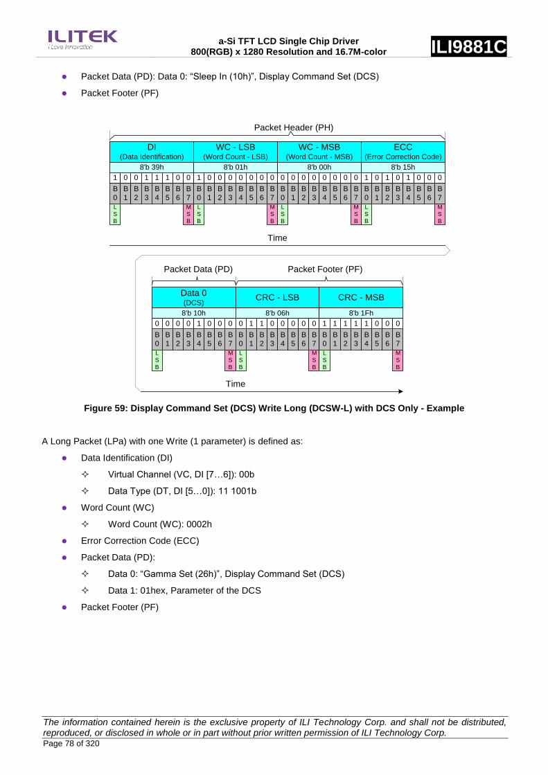
a-Si TFT LCD Single Chip Driver 800(RGB) x 1280 Resolution and 16.7M-color ILI9881C
The information contained herein is the exclusive property of ILI Technology Corp. and shall not be distributed, reproduced, or disclosed in whole or in part without prior written permission of ILI Technology Corp. Page 78 of 320
Packet Data (PD): Data 0: “Sleep In (10h)”, Display Command Set (DCS)
Packet Footer (PF)
Packet Header (PH)
DI (Data Identification)
B
0
B
1
B
2
B
3
B
4
B
5
B
7
B
6
WC - LSB(Word Count - LSB)
B
0
B
1
B
2
B
3
B
4
B
5
B
7
B
6
WC - MSB(Word Count - MSB)
B
0
B
1
B
2
B
3
B
4
B
5
B
7
B
6
B
0
B
1
B
2
B
3
B
4
B
5
B
7
B
6
ECC(Error Correction Code)
L
S
B
L
S
B
L
S
B
M
S
B
M
S
B
M
S
B
L
S
B
M
S
B
0 1
8'b 39h 8'b 01h 8'b 00h 8'b 15h
01 0 0 01 0 1 1 0 0 0 0 0 0 0 0 0 0 0 0 0 1 0 1 0 1 000
Time
Data 0(DCS)
B
0
B
1
B
2
B
3
B
4
B
5
B
7
B
6
CRC - LSB
B
0
B
1
B
2
B
3
B
4
B
5
B
7
B
6
B
0
B
1
B
2
B
3
B
4
B
5
B
7
B
6
CRC - MSB
L
S
B
L
S
B
M
S
B
M
S
B
L
S
B
M
S
B
8'b 10h 8'b 06h 8'b 1Fh
0 0 00 0 0 0 1 0 0 1 1 0 0 0 0 0 1 1 1 1 1 00
Time
Packet Data (PD) Packet Footer (PF)
Figure 59: Display Command Set (DCS) Write Long (DCSW-L) with DCS Only - Example
A Long Packet (LPa) with one Write (1 parameter) is defined as:
Data Identification (DI)
Virtual Channel (VC, DI [7…6]): 00b
Data Type (DT, DI [5…0]): 11 1001b
Word Count (WC)
Word Count (WC): 0002h
Error Correction Code (ECC)
Packet Data (PD):
Data 0: “Gamma Set (26h)”, Display Command Set (DCS)
Data 1: 01hex, Parameter of the DCS
Packet Footer (PF)
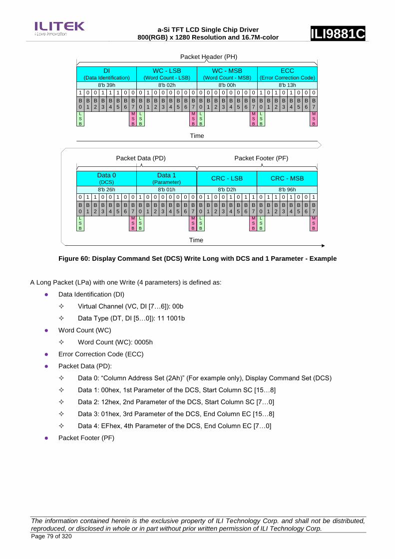
a-Si TFT LCD Single Chip Driver 800(RGB) x 1280 Resolution and 16.7M-color ILI9881C
The information contained herein is the exclusive property of ILI Technology Corp. and shall not be distributed, reproduced, or disclosed in whole or in part without prior written permission of ILI Technology Corp. Page 79 of 320
Packet Header (PH)
DI (Data Identification)
B
0
B
1
B
2
B
3
B
4
B
5
B
7
B
6
WC - LSB(Word Count - LSB)
B
0
B
1
B
2
B
3
B
4
B
5
B
7
B
6
WC - MSB(Word Count - MSB)
B
0
B
1
B
2
B
3
B
4
B
5
B
7
B
6
B
0
B
1
B
2
B
3
B
4
B
5
B
7
B
6
ECC(Error Correction Code)
L
S
B
L
S
B
L
S
B
M
S
B
M
S
B
M
S
B
L
S
B
M
S
B
0 1
8'b 39h 8'b 02h 8'b 00h 8'b 13h
01 0 0 01 0 1 0 1 0 0 0 0 0 0 0 0 0 0 0 0 1 0 1 0 1 000
Time
Data 0(DCS)
B
0
B
1
B
2
B
3
B
4
B
5
B
7
B
6
CRC - LSB
B
0
B
1
B
2
B
3
B
4
B
5
B
7
B
6
B
0
B
1
B
2
B
3
B
4
B
5
B
7
B
6
CRC - MSB
L
S
B
L
S
B
M
S
B
M
S
B
L
S
B
M
S
B
8'b 26h 8'b D2h 8'b 96h
0 0 00 1 1 0 0 1 0 1 0 0 1 0 1 1 0 1 1 0 1 10
Time
Packet Data (PD) Packet Footer (PF)
Data 1(Parameter)
B
0
B
1
B
2
B
3
B
4
B
5
B
7
B
6
L
S
B
M
S
B
8'b 01h
01 0 0 0 0 0 0
Figure 60: Display Command Set (DCS) Write Long with DCS and 1 Parameter - Example
A Long Packet (LPa) with one Write (4 parameters) is defined as:
Data Identification (DI)
Virtual Channel (VC, DI [7…6]): 00b
Data Type (DT, DI [5…0]): 11 1001b
Word Count (WC)
Word Count (WC): 0005h
Error Correction Code (ECC)
Packet Data (PD):
Data 0: “Column Address Set (2Ah)” (For example only), Display Command Set (DCS)
Data 1: 00hex, 1st Parameter of the DCS, Start Column SC [15…8]
Data 2: 12hex, 2nd Parameter of the DCS, Start Column SC [7…0]
Data 3: 01hex, 3rd Parameter of the DCS, End Column EC [15…8]
Data 4: EFhex, 4th Parameter of the DCS, End Column EC [7…0]
Packet Footer (PF)

a-Si TFT LCD Single Chip Driver 800(RGB) x 1280 Resolution and 16.7M-color ILI9881C
The information contained herein is the exclusive property of ILI Technology Corp. and shall not be distributed, reproduced, or disclosed in whole or in part without prior written permission of ILI Technology Corp. Page 80 of 320
Packet Header (PH)
DI (Data Identification)
B
0
B
1
B
2
B
3
B
4
B
5
B
7
B
6
WC - LSB(Word Count - LSB)
B
0
B
1
B
2
B
3
B
4
B
5
B
7
B
6
WC - MSB(Word Count - MSB)
B
0
B
1
B
2
B
3
B
4
B
5
B
7
B
6
B
0
B
1
B
2
B
3
B
4
B
5
B
7
B
6
ECC(Error Correction Code)
L
S
B
L
S
B
L
S
B
M
S
B
M
S
B
M
S
B
L
S
B
M
S
B
0 1
8'b 39h 8'b 05h 8'b 00h 8'b 36h
01 0 1 01 0 1 1 0 1 0 0 0 0 0 0 0 0 0 0 0 0 1 1 0 1 000
Time
Data 0(DCS)
B
0
B
1
B
2
B
3
B
4
B
5
B
7
B
6
Data 2(2nd Parameter)
B
0
B
1
B
2
B
3
B
4
B
5
B
7
B
6
B
0
B
1
B
2
B
3
B
4
B
5
B
7
B
6
Data 3(3rd Parameter)
L
S
B
L
S
B
M
S
B
M
S
B
L
S
B
M
S
B
8'b 2Ah 8'b 12h 8'b 01h
0 0 00 1 0 1 0 1 0 1 0 0 1 0 0 0 1 0 0 0 0 00
Time
Packet Data (PD)
Packet Footer (PF)
Data 1(1st Parameter)
B
0
B
1
B
2
B
3
B
4
B
5
B
7
B
6
L
S
B
M
S
B
8'b 00h
00 0 0 0 0 0 0
CRC - LSB
B
0
B
1
B
2
B
3
B
4
B
5
B
7
B
6
B
0
B
1
B
2
B
3
B
4
B
5
B
7
B
6
CRC - MSB
L
S
B
M
S
B
L
S
B
M
S
B
8'b BDh 8'b 2Ah
1 01 0 1 1 1 1 0 1 0 1 0 1 0 0
Data 4(4th Parameter)
B
0
B
1
B
2
B
3
B
4
B
5
B
7
B
6
L
S
B
M
S
B
8'b EFh
10 1 1 1 1 1 1
Packet Data (PD)
Time
Figure 61: Display Command Set (DCS) Write Long with DCS and 4 Parameters - Example

a-Si TFT LCD Single Chip Driver 800(RGB) x 1280 Resolution and 16.7M-color ILI9881C
The information contained herein is the exclusive property of ILI Technology Corp. and shall not be distributed, reproduced, or disclosed in whole or in part without prior written permission of ILI Technology Corp. Page 81 of 320
4.1.3.2.1.5. Display Command Set (DCS) Read, No Parameter (DCSRN-S)
“Display Command Set (DCS) Read, No Parameter” (DCSRN-S), which is defined in Data Type (DT, 00 0110b), is
always used in a Short Packet (SPa) from the MCU to the display module. These commands are defined in the
table below.
Table 13: Display Command Set (DCS) Read, No Parameter (DCSRN-S)
Command
Read Number of the Errors on DSI (05h)
Read Display Power Mode (0Ah)
Read Display MADCTL (0Bh)
Read Display Pixel Format (0Ch)
Read Display Image Mode (0Dh)
Read Display Signal Mode (0Eh)
Read Display Self-Diagnostic Result (0Fh)
Get Tear Scan Line(45h)
Read Display Brightness Value (52h)
Read CTRL Value Display (54h)
Read Power Save (56h)
Read CABC Minimum Brightness (5Fh)
Get Transition Time(69h)
Read Black/White Low Bits (70h)
Read Bkx (71h)
Read Bky(72h)
Read Wx (73h)
Read Wy (74h)
Read Red/Green Low Bits (75h)
Read Rx (76h)
Read Ry (77h)
Read Gx (78h)
Read Gy (79h)
Read Blue/A Color Low Bits (7Ah)
Read Bx (7Bh)
Read By (7Ch)
Read Ax (7Dh)
Read Ay (7Eh)
Read Idle Mode Color(81h)
Read DDB Start (A1h)
Read DDB Continue (A8h)
Read First Checksum(AAh)
Read Continue Checksum (AFh)
Read ID1 (DAh)
Read ID2 (DBh)
Read ID3 (DCh)
The MCU has to define to the display module the maximum size of the returned packet. The command, which is
used for this purpose, is “Set Maximum Return Packet Size” (SMRPS-S), which Data Type (DT) is 11 0111b and is
used in a Short Packet (SPa) before the MCU can send “Display Command Set (DCS) Read, No Parameter” to the
display module. This sequence is illustrated for reference purposes below.
Step 1:

a-Si TFT LCD Single Chip Driver 800(RGB) x 1280 Resolution and 16.7M-color ILI9881C
The information contained herein is the exclusive property of ILI Technology Corp. and shall not be distributed, reproduced, or disclosed in whole or in part without prior written permission of ILI Technology Corp. Page 82 of 320
The MCU sends “Set Maximum Return Packet Size” (Short Packet (SPa)) (SMRPS-S) to the display module when
it wants to return one byte from the display module.
Data Identification (DI)
Virtual Channel (VC, DI [7…6]): 00b
Data Type (DT, DI [5…0]): 11 0111b
Maximum Return Packet Size (MRPS)
Data 0: 01hex
Data 1: 00hex
Error Correction Code (ECC)
DI (Data Identification)
B
0
B
1
B
2
B
3
B
4
B
5
B
7
B
6
MRPS - LSB
B
0
B
1
B
2
B
3
B
4
B
5
B
7
B
6
MRPS - MSB
B
0
B
1
B
2
B
3
B
4
B
5
B
7
B
6
B
0
B
1
B
2
B
3
B
4
B
5
B
7
B
6
ECC(Error Correction Code)
L
S
B
L
S
B
L
S
B
M
S
B
M
S
B
M
S
B
L
S
B
M
S
B
1 0
8'b 37h 8'b 01h 8'b 00h 8'b 1Dh
01 0 0 01 1 1 1 0 0 0 0 0 0 0 0 0 0 0 0 0 1 0 1 1 1 000
Time
Packet Header (PH)
Maximum Return Packet Size (MRPS)
Figure 62: Set Maximum Return Packet Size (SMRPS-S) - Example
Step 2:
The MCU wants to receive the value of the “Read ID1 (DAh)” from the display module when the MCU sends
“Display Command Set (DCS) Read, No Parameter” to the display module.
Data Identification (DI)
Virtual Channel (VC, DI [7…6]): 00b
Data Type (DT, DI [5…0]): 00 0110b
Packet Data (PD)
Data 0: “Read ID1 (DAh)”, Display Command Set (DCS)
Data 1: Always 00hex
Error Correction Code (ECC)

a-Si TFT LCD Single Chip Driver 800(RGB) x 1280 Resolution and 16.7M-color ILI9881C
The information contained herein is the exclusive property of ILI Technology Corp. and shall not be distributed, reproduced, or disclosed in whole or in part without prior written permission of ILI Technology Corp. Page 83 of 320
DI (Data Identification)
B
0
B
1
B
2
B
3
B
4
B
5
B
7
B
6
Data 0(DCS)
B
0
B
1
B
2
B
3
B
4
B
5
B
7
B
6
Data 1(Always 8'b 00h)
B
0
B
1
B
2
B
3
B
4
B
5
B
7
B
6
B
0
B
1
B
2
B
3
B
4
B
5
B
7
B
6
ECC(Error Correction Code)
L
S
B
L
S
B
L
S
B
M
S
B
M
S
B
M
S
B
L
S
B
M
S
B
1 0
8'b 06h 8'b DAh 8'b 00h 8'b 1Fh
00 1 0 00 1 0 0 1 0 1 1 0 0 0 0 0 0 0 0 0 1 1 1 1 1 010
Time
Packet Header (PH)
Packet Data (PD)
Figure 63: Display Command Set (DCS) Read, No Parameter (DCSRN-S) - Example
Step 3:
The display module can send 2 different information to the MCU after Bus Turnaround (BTA):
1. An acknowledge with Error Report (AwER), which is used in a Short Packet (SPa), if there is an error when
receiving a command. See the section “4.1.3.2.2.2 Acknowledge with Error Report (AwER)”.
2. Information of the received command, which can be a Short Packet (SPa) or a Long Packet (LPa).

a-Si TFT LCD Single Chip Driver 800(RGB) x 1280 Resolution and 16.7M-color ILI9881C
The information contained herein is the exclusive property of ILI Technology Corp. and shall not be distributed, reproduced, or disclosed in whole or in part without prior written permission of ILI Technology Corp. Page 84 of 320
4.1.3.2.1.6. Null Packet, No Data (NP-L)
“Null Packet, No Data” (NP-L), which is defined in Data Type (DT, 001001b), is always used in a Long Packet (LPa)
from the MCU to the display module. The purpose of this command is to keep data lanes in the high speed mode
(HSDT) if necessary. The display module can ignore the Packet Data (PD) that the MCU sends.
A Long Packet (LPa) with 5 random data bytes of the Packet Data (PD) is defined as:
Data Identification (DI)
Virtual Channel (VC, DI [7…6]): 00b
Data Type (DT, DI [5…0]): 00 1001b
Word Count (WC)
Word Count (WC): 0005hex
Error Correction Code (ECC)
Packet Data (PD):
Data 0: 89hex (Random data)
Data 1: 23hex (Random data)
Data 2: 12hex (Random data)
Data 3: A2hex (Random data)
Data 4: E2hex (Random data)
Packet Footer (PF)
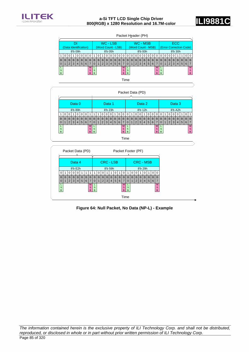
a-Si TFT LCD Single Chip Driver 800(RGB) x 1280 Resolution and 16.7M-color ILI9881C
The information contained herein is the exclusive property of ILI Technology Corp. and shall not be distributed, reproduced, or disclosed in whole or in part without prior written permission of ILI Technology Corp. Page 85 of 320
Packet Header (PH)
DI (Data Identification)
B
0
B
1
B
2
B
3
B
4
B
5
B
7
B
6
WC - LSB(Word Count - LSB)
B
0
B
1
B
2
B
3
B
4
B
5
B
7
B
6
WC - MSB(Word Count - MSB)
B
0
B
1
B
2
B
3
B
4
B
5
B
7
B
6
B
0
B
1
B
2
B
3
B
4
B
5
B
7
B
6
ECC(Error Correction Code)
L
S
B
L
S
B
L
S
B
M
S
B
M
S
B
M
S
B
L
S
B
M
S
B
0 1
8'b 09h 8'b 05h 8'b 00h 8'b 30h
00 0 1 01 0 0 1 0 1 0 0 0 0 0 0 0 0 0 0 0 0 0 0 0 1 000
Time
Data 0
B
0
B
1
B
2
B
3
B
4
B
5
B
7
B
6
Data 2
B
0
B
1
B
2
B
3
B
4
B
5
B
7
B
6
B
0
B
1
B
2
B
3
B
4
B
5
B
7
B
6
Data 3
L
S
B
L
S
B
M
S
B
M
S
B
L
S
B
M
S
B
8'b 89h 8'b 12h 8'b A2h
1 1 01 0 0 1 0 0 0 1 0 0 1 0 0 0 0 1 0 0 0 10
Time
Packet Data (PD)
Packet Footer (PF)
Data 1
B
0
B
1
B
2
B
3
B
4
B
5
B
7
B
6
L
S
B
M
S
B
8'b 23h
01 1 0 0 0 1 0
CRC - LSB
B
0
B
1
B
2
B
3
B
4
B
5
B
7
B
6
B
0
B
1
B
2
B
3
B
4
B
5
B
7
B
6
CRC - MSB
L
S
B
M
S
B
L
S
B
M
S
B
8'b 59h 8'b 29h
1 01 0 0 1 1 0 1 0 1 0 0 1 0 0
Data 4
B
0
B
1
B
2
B
3
B
4
B
5
B
7
B
6
L
S
B
M
S
B
8'b E2h
10 1 0 0 0 1 1
Packet Data (PD)
Time
Figure 64: Null Packet, No Data (NP-L) - Example

a-Si TFT LCD Single Chip Driver 800(RGB) x 1280 Resolution and 16.7M-color ILI9881C
The information contained herein is the exclusive property of ILI Technology Corp. and shall not be distributed, reproduced, or disclosed in whole or in part without prior written permission of ILI Technology Corp. Page 86 of 320
4.1.3.2.1.7. End of Transmission Packet (EoTP)
“End of Transmission Packet” (EoTP), which is an interface level function and defined in Data Type (DT, 00 1000b),
is always used in a Short Packet (SPa) from the MCU to the display module. The purpose of this command is to
terminate the high Speed Data Transmission (HSDT) mode properly when EoTP is added after the last payload
packet before “End of Transmission” (EoT).
The MCU can decide if it wants to use the “End of Transmission Packet” (EoTP) or not. The display shall have the
capability to support both. That is, if the MCU applies the EoTP, it shall report the “DSI Protocol Violation Error”
when the EoTP is not detected in the High-Speed (HS). The display module error reporting shall be
enabled/disabled statistically, according to the module application.
The display module does or does not receive “End of Transmission Packet” (EoTP) from the MCU during the Low
Power Data Transmission (LPDT) mode before “Mark-1” (= leaving the Escape mode) which ends the Low Power
Data Transmission (LPDT) mode. The display module is not allowed to send “End of Transmission Packet” (EoTP)
to the MCU during the Low Power Data Transmission (LPDT) mode. The summary of the receiving and
transmitting EoTP is listed below.
Table 14: Receiving and Transmitting EoTP during LPDT
Direction Display Module (DM) in
High Speed Data Transmission (HSDT)
Display Module (DM) in
Low Power Data Transmission (LPDT)
MCU => Display Module Support With and Without EoTP Support With and Without EoTP
Display Module => MCU HS Mode is not available
(EoTP is not available)
EoTP cannot be sent by the Display Module
(DM)
A Short Packet (SPa) using a fixed format is as follows:
Data Identification (DI)
Virtual Channel (VC, DI [7…6]): 00b
Data Type (DT, DI [5…0]): 00 1000b
Packet Data (PD)
Data 0: 0Fhex
Data 1: 0Fhex
Error Correction Code (ECC)
ECC: 01hex
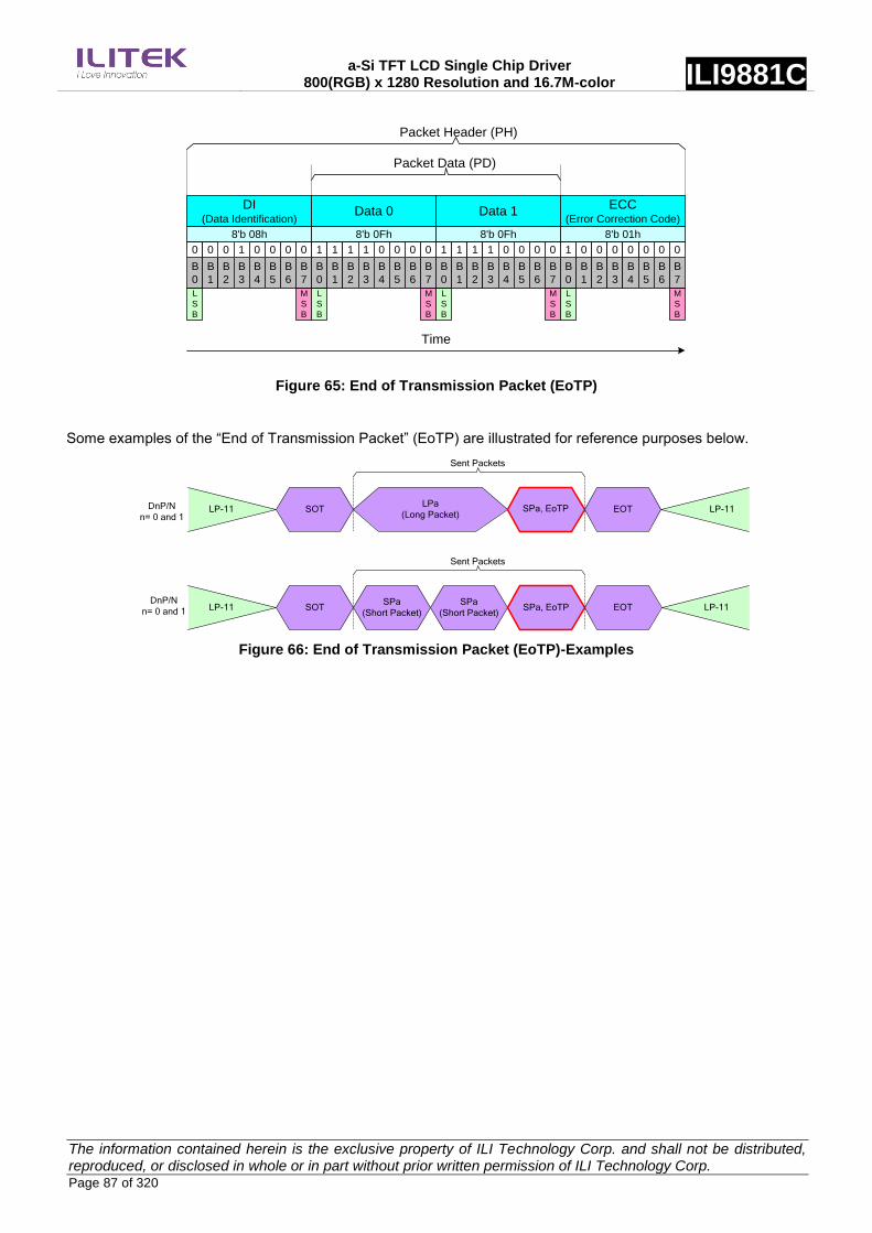
a-Si TFT LCD Single Chip Driver 800(RGB) x 1280 Resolution and 16.7M-color ILI9881C
The information contained herein is the exclusive property of ILI Technology Corp. and shall not be distributed, reproduced, or disclosed in whole or in part without prior written permission of ILI Technology Corp. Page 87 of 320
DI (Data Identification)
B
0
B
1
B
2
B
3
B
4
B
5
B
7
B
6
Data 0
B
0
B
1
B
2
B
3
B
4
B
5
B
7
B
6
Data 1
B
0
B
1
B
2
B
3
B
4
B
5
B
7
B
6
B
0
B
1
B
2
B
3
B
4
B
5
B
7
B
6
ECC(Error Correction Code)
L
S
B
L
S
B
L
S
B
M
S
B
M
S
B
M
S
B
L
S
B
M
S
B
0 1
8'b 08h 8'b 0Fh 8'b 0Fh 8'b 01h
00 0 0 00 0 0 1 1 1 1 0 0 1 1 1 1 0 0 0 0 1 0 0 0 0 000
Time
Packet Header (PH)
Packet Data (PD)
Figure 65: End of Transmission Packet (EoTP)
Some examples of the “End of Transmission Packet” (EoTP) are illustrated for reference purposes below.
LP-11 LP-11
LP-11 LP-11
DnP/N
n= 0 and 1SOT
LPa
(Long Packet)EOT
SOT EOTSPa
(Short Packet)
SPa
(Short Packet)SPa, EoTP
Sent Packets
Sent Packets
DnP/N
n= 0 and 1
SPa, EoTP
Figure 66: End of Transmission Packet (EoTP)-Examples
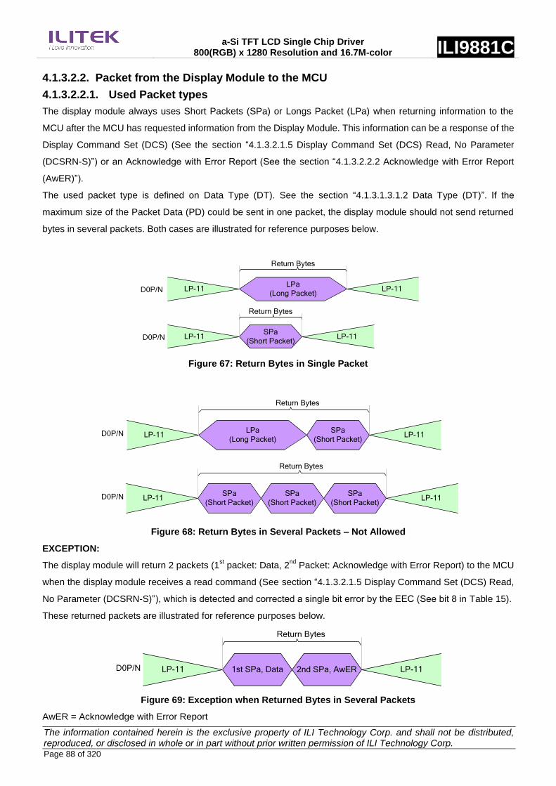
a-Si TFT LCD Single Chip Driver 800(RGB) x 1280 Resolution and 16.7M-color ILI9881C
The information contained herein is the exclusive property of ILI Technology Corp. and shall not be distributed, reproduced, or disclosed in whole or in part without prior written permission of ILI Technology Corp. Page 88 of 320
4.1.3.2.2. Packet from the Display Module to the MCU
4.1.3.2.2.1. Used Packet types
The display module always uses Short Packets (SPa) or Longs Packet (LPa) when returning information to the
MCU after the MCU has requested information from the Display Module. This information can be a response of the
Display Command Set (DCS) (See the section “4.1.3.2.1.5 Display Command Set (DCS) Read, No Parameter
(DCSRN-S)”) or an Acknowledge with Error Report (See the section “4.1.3.2.2.2 Acknowledge with Error Report
(AwER)”).
The used packet type is defined on Data Type (DT). See the section “4.1.3.1.3.1.2 Data Type (DT)”. If the
maximum size of the Packet Data (PD) could be sent in one packet, the display module should not send returned
bytes in several packets. Both cases are illustrated for reference purposes below.
LP-11 LP-11
LP-11 LP-11
D0P/NLPa
(Long Packet)
SPa
(Short Packet)
Return Bytes
Return Bytes
D0P/N
Figure 67: Return Bytes in Single Packet
D0P/N
D0P/N
LP-11 LP-11
LP-11 LP-11
LPa
(Long Packet)
SPa
(Short Packet)
Return Bytes
Return Bytes
SPa
(Short Packet)
SPa
(Short Packet)
SPa
(Short Packet)
LP-11
Figure 68: Return Bytes in Several Packets – Not Allowed
EXCEPTION:
The display module will return 2 packets (1st packet: Data, 2
nd Packet: Acknowledge with Error Report) to the MCU
when the display module receives a read command (See section “4.1.3.2.1.5 Display Command Set (DCS) Read,
No Parameter (DCSRN-S)”), which is detected and corrected a single bit error by the EEC (See bit 8 in Table 15).
These returned packets are illustrated for reference purposes below.
D0P/N LP-11 LP-111st SPa, Data
Return Bytes
2nd SPa, AwER
Figure 69: Exception when Returned Bytes in Several Packets
AwER = Acknowledge with Error Report
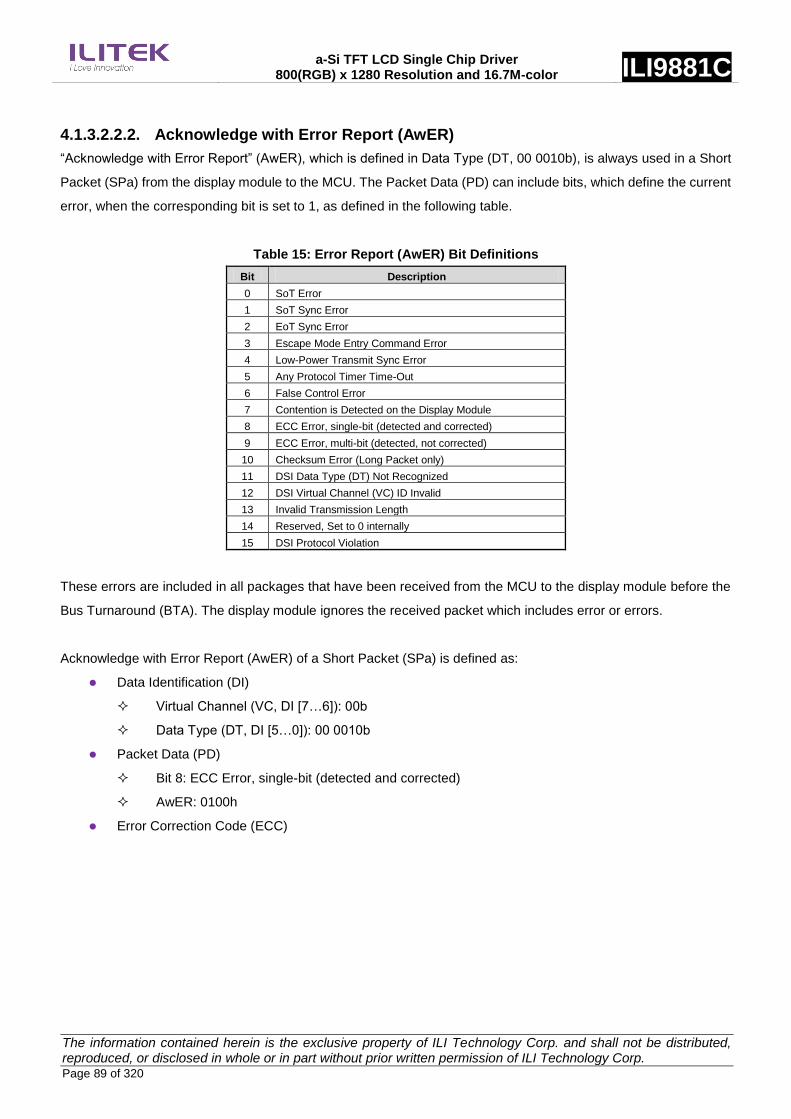
a-Si TFT LCD Single Chip Driver 800(RGB) x 1280 Resolution and 16.7M-color ILI9881C
The information contained herein is the exclusive property of ILI Technology Corp. and shall not be distributed, reproduced, or disclosed in whole or in part without prior written permission of ILI Technology Corp. Page 89 of 320
4.1.3.2.2.2. Acknowledge with Error Report (AwER)
“Acknowledge with Error Report” (AwER), which is defined in Data Type (DT, 00 0010b), is always used in a Short
Packet (SPa) from the display module to the MCU. The Packet Data (PD) can include bits, which define the current
error, when the corresponding bit is set to 1, as defined in the following table.
Table 15: Error Report (AwER) Bit Definitions
Bit Description
0 SoT Error
1 SoT Sync Error
2 EoT Sync Error
3 Escape Mode Entry Command Error
4 Low-Power Transmit Sync Error
5 Any Protocol Timer Time-Out
6 False Control Error
7 Contention is Detected on the Display Module
8 ECC Error, single-bit (detected and corrected)
9 ECC Error, multi-bit (detected, not corrected)
10 Checksum Error (Long Packet only)
11 DSI Data Type (DT) Not Recognized
12 DSI Virtual Channel (VC) ID Invalid
13 Invalid Transmission Length
14 Reserved, Set to 0 internally
15 DSI Protocol Violation
These errors are included in all packages that have been received from the MCU to the display module before the
Bus Turnaround (BTA). The display module ignores the received packet which includes error or errors.
Acknowledge with Error Report (AwER) of a Short Packet (SPa) is defined as:
Data Identification (DI)
Virtual Channel (VC, DI [7…6]): 00b
Data Type (DT, DI [5…0]): 00 0010b
Packet Data (PD)
Bit 8: ECC Error, single-bit (detected and corrected)
AwER: 0100h
Error Correction Code (ECC)

a-Si TFT LCD Single Chip Driver 800(RGB) x 1280 Resolution and 16.7M-color ILI9881C
The information contained herein is the exclusive property of ILI Technology Corp. and shall not be distributed, reproduced, or disclosed in whole or in part without prior written permission of ILI Technology Corp. Page 90 of 320
DI (Data Identification)
B
0
B
1
B
2
B
3
B
4
B
5
B
7
B
6
AwER - LSB
B
0
B
1
B
2
B
3
B
4
B
5
B
7
B
6
AwER - MSB
B
0
B
1
B
2
B
3
B
4
B
5
B
7
B
6
B
0
B
1
B
2
B
3
B
4
B
5
B
7
B
6
ECC(Error Correction Code)
L
S
B
L
S
B
L
S
B
M
S
B
M
S
B
M
S
B
L
S
B
M
S
B
0 0
8'b 02h 8'b 00h 8'b 01h 8'b 3Ah
00 0 1 00 1 0 0 0 0 0 0 0 1 0 0 0 0 0 0 0 0 1 0 1 1 000
Time
Packet Header (PH)
Packet Data (PD)
Figure 70: Acknowledge with Error Report (AwER) – Example
It is possible that the display module receives several packets, which include errors, from the MCU before the MCU
performs the Bus Turnaround (BTA). Some examples are illustrated for reference purposes below.
LP-11 LP-11
LP-11 LP-11
DnP/N
n= 0 and 1
LPa
(Long Packet)
SOT
Packets from the MCU
Packets from the MCU
SPa
(Short Packet)
SPa
(Short Packet)
SPa
(Short Packet)
LP-11EOT
EOT
Includes an error
Includes an error
BTASOT
SPa
(Short Packet)BTA
DnP/N
n= 0 and 1
Figure 71: Errors Packets
Therefore, a method is needed to check if there are errors in the previous packets. These errors of the previous
packets can be detected by “Read Display Signal Mode (0Eh)” and “Read Number of the Errors on DSI (05h)”
commands. The bit D0 of the “Read Display Signal Mode (0Eh)” command will be set to 1 if a received packet
includes an error.
The amount of packets, which include an ECC or CRC error, is calculated in the RDNUMED register, which can
read “Read Number of the Errors on DSI (05h)” command. This command also sets the RDNUMED register to 00h
and set the bit D0 of the “Read Display Signal Mode (0Eh)” command to 0 after the MCU has read the RDNUMED
register from the display module. The functionality of the RDNUMED register is illustrated for reference purposes
below.
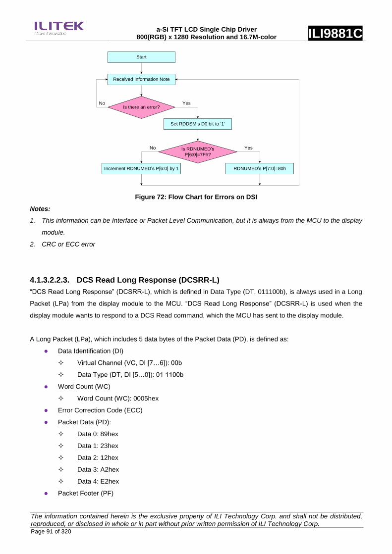
a-Si TFT LCD Single Chip Driver 800(RGB) x 1280 Resolution and 16.7M-color ILI9881C
The information contained herein is the exclusive property of ILI Technology Corp. and shall not be distributed, reproduced, or disclosed in whole or in part without prior written permission of ILI Technology Corp. Page 91 of 320
Start
Received Information Note
Set RDDSM‟s D0 bit to ‟1‟
RDNUMED‟s P[7:0]=80hIncrement RDNUMED‟s P[6:0] by 1
Is there an error?
Is RDNUMED‟s
P[6:0]=7Fh?
No Yes
No Yes
Figure 72: Flow Chart for Errors on DSI
Notes:
1. This information can be Interface or Packet Level Communication, but it is always from the MCU to the display
module.
2. CRC or ECC error
4.1.3.2.2.3. DCS Read Long Response (DCSRR-L)
“DCS Read Long Response” (DCSRR-L), which is defined in Data Type (DT, 011100b), is always used in a Long
Packet (LPa) from the display module to the MCU. “DCS Read Long Response” (DCSRR-L) is used when the
display module wants to respond to a DCS Read command, which the MCU has sent to the display module.
A Long Packet (LPa), which includes 5 data bytes of the Packet Data (PD), is defined as:
Data Identification (DI)
Virtual Channel (VC, DI [7…6]): 00b
Data Type (DT, DI [5…0]): 01 1100b
Word Count (WC)
Word Count (WC): 0005hex
Error Correction Code (ECC)
Packet Data (PD):
Data 0: 89hex
Data 1: 23hex
Data 2: 12hex
Data 3: A2hex
Data 4: E2hex
Packet Footer (PF)

a-Si TFT LCD Single Chip Driver 800(RGB) x 1280 Resolution and 16.7M-color ILI9881C
The information contained herein is the exclusive property of ILI Technology Corp. and shall not be distributed, reproduced, or disclosed in whole or in part without prior written permission of ILI Technology Corp. Page 92 of 320
Packet Header (PH)
DI (Data Identification)
B
0
B
1
B
2
B
3
B
4
B
5
B
7
B
6
WC - LSB(Word Count - LSB)
B
0
B
1
B
2
B
3
B
4
B
5
B
7
B
6
WC - MSB(Word Count - MSB)
B
0
B
1
B
2
B
3
B
4
B
5
B
7
B
6
B
0
B
1
B
2
B
3
B
4
B
5
B
7
B
6
ECC(Error Correction Code)
L
S
B
L
S
B
L
S
B
M
S
B
M
S
B
M
S
B
L
S
B
M
S
B
1 1
8'b 1Ch 8'b 05h 8'b 00h 8'b 29h
01 0 1 00 0 0 1 0 1 0 0 0 0 0 0 0 0 0 0 0 1 0 0 1 0 000
Time
Data 0
B
0
B
1
B
2
B
3
B
4
B
5
B
7
B
6
Data 2
B
0
B
1
B
2
B
3
B
4
B
5
B
7
B
6
B
0
B
1
B
2
B
3
B
4
B
5
B
7
B
6
Data 3
L
S
B
L
S
B
M
S
B
M
S
B
L
S
B
M
S
B
8'b 89h 8'b 12h 8'b A2h
1 1 01 0 0 1 0 0 0 1 0 0 1 0 0 0 0 1 0 0 0 10
Time
Packet Data (PD)
Packet Footer (PF)
Data 1
B
0
B
1
B
2
B
3
B
4
B
5
B
7
B
6
L
S
B
M
S
B
8'b 23h
01 1 0 0 0 1 0
CRC - LSB
B
0
B
1
B
2
B
3
B
4
B
5
B
7
B
6
B
0
B
1
B
2
B
3
B
4
B
5
B
7
B
6
CRC - MSB
L
S
B
M
S
B
L
S
B
M
S
B
8'b 59h 8'b 29h
1 01 0 0 1 1 0 1 0 1 0 0 1 0 0
Data 4
B
0
B
1
B
2
B
3
B
4
B
5
B
7
B
6
L
S
B
M
S
B
8'b E2h
10 1 0 0 0 1 1
Packet Data (PD)
Time
Figure 73: DCS Read Long Response (DCSRR-L) - Example

a-Si TFT LCD Single Chip Driver 800(RGB) x 1280 Resolution and 16.7M-color ILI9881C
The information contained herein is the exclusive property of ILI Technology Corp. and shall not be distributed, reproduced, or disclosed in whole or in part without prior written permission of ILI Technology Corp. Page 93 of 320
4.1.3.2.2.4. DCS Read Short Response, 1 Byte Returned (DCSRR1-S)
“DCS Read Short Response, 1 Byte Returned” (DCSRR1-S), which is defined in Data Type (DT, 10 0001b), is
always used in a Short Packet (SPa) from the display module to the MCU. “DCS Read Short Response, 1 Byte
Returned (DCSRR1-S) is used when the display module wants to respond to a DCS Read command, which the
MCU has sent to the display module.
A Short Packet (SPa) is defined as:
Data Identification (DI)
Virtual Channel (VC, DI [7…6]): 00b
Data Type (DT, DI [5…0]): 10 0001b
Packet Data (PD)
Data 0: 45hex
Data 1: 00hex (Always)
Error Correction Code (ECC)
DI (Data Identification)
B
0
B
1
B
2
B
3
B
4
B
5
B
7
B
6
Data 0(Packet Data)
B
0
B
1
B
2
B
3
B
4
B
5
B
7
B
6
Data 1(Always 8'b 00h)
B
0
B
1
B
2
B
3
B
4
B
5
B
7
B
6
B
0
B
1
B
2
B
3
B
4
B
5
B
7
B
6
ECC(Error Correction Code)
L
S
B
L
S
B
L
S
B
M
S
B
M
S
B
M
S
B
L
S
B
M
S
B
0 0
8'b 21h 8'b 45h 8'b 00h 8'b 01h
00 0 0 01 0 1 1 0 1 0 0 0 0 0 0 0 0 0 0 0 1 0 0 0 0 010
Time
Packet Header (PH)
Packet Data (PD)
Figure 74: DCS Read Short Response, 1 Byte Returned (DCSRR1-S) - Example

a-Si TFT LCD Single Chip Driver 800(RGB) x 1280 Resolution and 16.7M-color ILI9881C
The information contained herein is the exclusive property of ILI Technology Corp. and shall not be distributed, reproduced, or disclosed in whole or in part without prior written permission of ILI Technology Corp. Page 94 of 320
4.1.3.2.2.5. DCS Read Short Response, 2 Bytes Returned (DCSRR2-S)
“DCS Read Short Response, 2 Bytes Returned” (DCSRR2-S), which is defined in Data Type (DT, 10 0010b), is
always used in a Short Packet (SPa) from the display module to the MCU. “DCS Read Short Response, 2 Bytes
Returned” (DCSRR2-S) is used when the display module wants to respond to a DCS Read command, which the
MCU has sent to the display module.
A Short Packet (SPa) is defined as:
Data Identification (DI)
Virtual Channel (VC, DI [7…6]): 00b
Data Type (DT, DI [5…0]): 10 0010b
Packet Data (PD)
Data 0: 45hex
Data 1: 32hex
Error Correction Code (ECC)
Packet Header (PH)
Packet Data (PD)
DI (Data Identification)
B
0
B
1
B
2
B
3
B
4
B
5
B
7
B
6
Data 0(Packet Data)
B
0
B
1
B
2
B
3
B
4
B
5
B
7
B
6
Data 1(Always 8'b 00h)
B
0
B
1
B
2
B
3
B
4
B
5
B
7
B
6
B
0
B
1
B
2
B
3
B
4
B
5
B
7
B
6
ECC(Error Correction Code)
L
S
B
L
S
B
L
S
B
M
S
B
M
S
B
M
S
B
L
S
B
M
S
B
0 0
8'b 22h 8'b 45h 8'b 32h 8'b 0Fh
00 0 0 00 1 1 1 0 1 0 0 0 0 1 0 0 1 1 0 0 1 1 1 1 0 010
Time
Packet Header (PH)
Packet Data (PD)
DI (Data Identification)
B
0
B
1
B
2
B
3
B
4
B
5
B
7
B
6
Data 0(Packet Data)
B
0
B
1
B
2
B
3
B
4
B
5
B
7
B
6
Data 1(Always 8'b 00h)
B
0
B
1
B
2
B
3
B
4
B
5
B
7
B
6
B
0
B
1
B
2
B
3
B
4
B
5
B
7
B
6
ECC(Error Correction Code)
L
S
B
L
S
B
L
S
B
M
S
B
M
S
B
M
S
B
L
S
B
M
S
B
0 0
8'b 22h 8'b 45h 8'b 32h 8'b 0Fh
00 0 0 00 1 1 1 0 1 0 0 0 0 1 0 0 1 1 0 0 1 1 1 1 0 010
Time
Figure 75: DCS Read Short Response, 2 Bytes Returned (DCSRR2-S) - Example
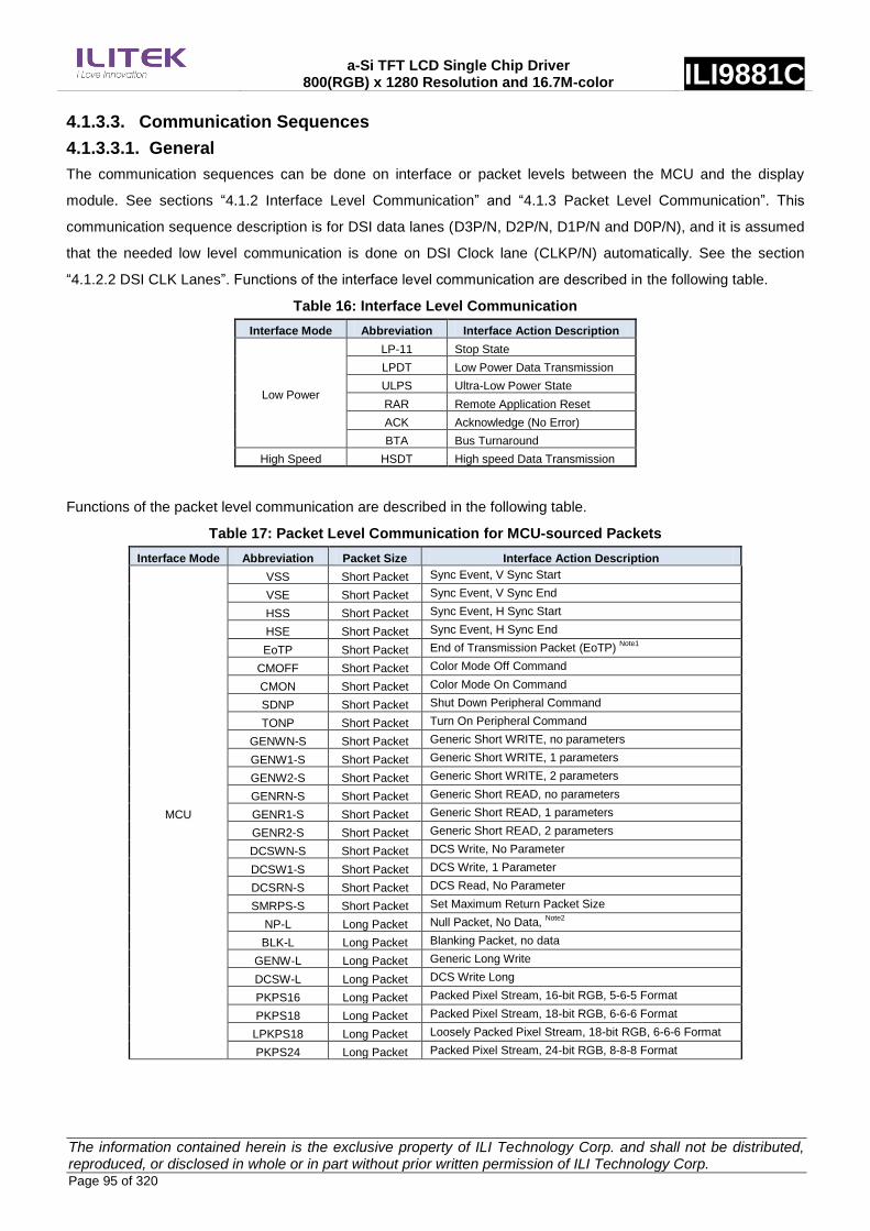
a-Si TFT LCD Single Chip Driver 800(RGB) x 1280 Resolution and 16.7M-color ILI9881C
The information contained herein is the exclusive property of ILI Technology Corp. and shall not be distributed, reproduced, or disclosed in whole or in part without prior written permission of ILI Technology Corp. Page 95 of 320
4.1.3.3. Communication Sequences
4.1.3.3.1. General
The communication sequences can be done on interface or packet levels between the MCU and the display
module. See sections “4.1.2 Interface Level Communication” and “4.1.3 Packet Level Communication”. This
communication sequence description is for DSI data lanes (D3P/N, D2P/N, D1P/N and D0P/N), and it is assumed
that the needed low level communication is done on DSI Clock lane (CLKP/N) automatically. See the section
“4.1.2.2 DSI CLK Lanes”. Functions of the interface level communication are described in the following table.
Table 16: Interface Level Communication
Interface Mode Abbreviation Interface Action Description
Low Power
LP-11 Stop State
LPDT Low Power Data Transmission
ULPS Ultra-Low Power State
RAR Remote Application Reset
ACK Acknowledge (No Error)
BTA Bus Turnaround
High Speed HSDT High speed Data Transmission
Functions of the packet level communication are described in the following table.
Table 17: Packet Level Communication for MCU-sourced Packets
Interface Mode Abbreviation Packet Size Interface Action Description
MCU
VSS Short Packet Sync Event, V Sync Start
VSE Short Packet Sync Event, V Sync End
HSS Short Packet Sync Event, H Sync Start
HSE Short Packet Sync Event, H Sync End
EoTP Short Packet End of Transmission Packet (EoTP) Note1
CMOFF Short Packet Color Mode Off Command
CMON Short Packet Color Mode On Command
SDNP Short Packet Shut Down Peripheral Command
TONP Short Packet Turn On Peripheral Command
GENWN-S Short Packet Generic Short WRITE, no parameters
GENW1-S Short Packet Generic Short WRITE, 1 parameters
GENW2-S Short Packet Generic Short WRITE, 2 parameters
GENRN-S Short Packet Generic Short READ, no parameters
GENR1-S Short Packet Generic Short READ, 1 parameters
GENR2-S Short Packet Generic Short READ, 2 parameters
DCSWN-S Short Packet DCS Write, No Parameter
DCSW1-S Short Packet DCS Write, 1 Parameter
DCSRN-S Short Packet DCS Read, No Parameter
SMRPS-S Short Packet Set Maximum Return Packet Size
NP-L Long Packet Null Packet, No Data, Note2
BLK-L Long Packet Blanking Packet, no data
GENW-L Long Packet Generic Long Write
DCSW-L Long Packet DCS Write Long
PKPS16 Long Packet Packed Pixel Stream, 16-bit RGB, 5-6-5 Format
PKPS18 Long Packet Packed Pixel Stream, 18-bit RGB, 6-6-6 Format
LPKPS18 Long Packet Loosely Packed Pixel Stream, 18-bit RGB, 6-6-6 Format
PKPS24 Long Packet Packed Pixel Stream, 24-bit RGB, 8-8-8 Format

a-Si TFT LCD Single Chip Driver 800(RGB) x 1280 Resolution and 16.7M-color ILI9881C
The information contained herein is the exclusive property of ILI Technology Corp. and shall not be distributed, reproduced, or disclosed in whole or in part without prior written permission of ILI Technology Corp. Page 96 of 320
Table 18: Packet Level Communication for Peripheral-sourced packets
Interface Mode Abbreviation Packet Size Interface Action Description
Display Module
(ILI9881C)
AwER Short Packet Acknowledge with Error Report
EoTP Short Packet End of Transmission Packet
GENRR1-S Short Packet Generic Short READ Response, 1 byte returned
GENRR2-S Short Packet Generic Short READ Response, 2 byte returned
GENRR-L Long Packet Generic Long READ Response
DCSRR-L Long Packet DCS Read Long Response
DCSRR1-S Short Packet DCS Read Short Response, 1 byte returned
DCSRR2-S Short Packet DCS Read Short Response, 2 byte returned
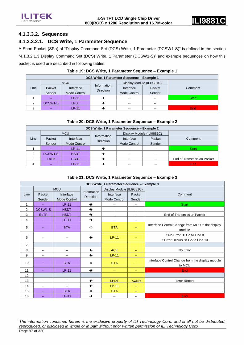
a-Si TFT LCD Single Chip Driver 800(RGB) x 1280 Resolution and 16.7M-color ILI9881C
The information contained herein is the exclusive property of ILI Technology Corp. and shall not be distributed, reproduced, or disclosed in whole or in part without prior written permission of ILI Technology Corp. Page 97 of 320
4.1.3.3.2. Sequences
4.1.3.3.2.1. DCS Write, 1 Parameter Sequence
A Short Packet (SPa) of “Display Command Set (DCS) Write, 1 Parameter (DCSW1-S)” is defined in the section
“4.1.3.2.1.3 Display Command Set (DCS) Write, 1 Parameter (DCSW1-S)” and example sequences on how this
packet is used are described in following tables.
Table 19: DCS Write, 1 Parameter Sequence – Example 1
DCS Write, 1 Parameter Sequence – Example 1
Line
MCU Information
Direction
Display Module (ILI9881C)
Comment Packet
Sender
Interface
Mode Control
Interface
Mode Control
Packet
Sender
1 -- LP-11 -- -- Start
2 DCSW1-S LPDT -- --
3 -- LP-11 -- -- End
Table 20: DCS Write, 1 Parameter Sequence – Example 2
DCS Write, 1 Parameter Sequence – Example 2
Line
MCU Information
Direction
Display Module (ILI9881C)
Comment Packet
Sender
Interface
Mode Control
Interface
Mode Control
Packet
Sender
1 -- LP-11 -- -- Start
2 DCSW1-S HSDT -- --
3 EoTP HSDT -- -- End of Transmission Packet
4 -- LP-11 -- -- End
Table 21: DCS Write, 1 Parameter Sequence – Example 3
DCS Write, 1 Parameter Sequence – Example 3
Line
MCU Information
Direction
Display Module (ILI9881C)
Comment Packet
Sender
Interface
Mode Control
Interface
Mode Control
Packet
Sender
1 -- LP-11 -- -- Start
2 DCSW1-S HSDT -- --
3 EoTP HSDT -- -- End of Transmission Packet
4 -- LP-11 -- --
5 -- BTA BTA -- Interface Control Change from MCU to the display
module
6 -- -- LP-11 -- If No Error Go to Line 8
If Error Occurs Go to Line 13
7
8 -- -- ACK -- No Error
9 -- -- LP-11 --
10 -- BTA BTA -- Interface Control Change from the display module
to MCU
11 -- LP-11 -- -- End
12
13 -- -- LPDT AwER Error Report
14 -- -- LP-11 --
15 -- BTA BTA --
16 -- LP-11 -- -- End

a-Si TFT LCD Single Chip Driver 800(RGB) x 1280 Resolution and 16.7M-color ILI9881C
The information contained herein is the exclusive property of ILI Technology Corp. and shall not be distributed, reproduced, or disclosed in whole or in part without prior written permission of ILI Technology Corp. Page 98 of 320
4.1.3.3.2.2. DCS Write, No Parameter Sequence
A Short Packet (SPa) of “Display Command Set (DCS) Write, No Parameter (DCSWN-S)” is defined in the section
“4.1.3.2.1.2 Display Command Set (DCS) Write, No Parameter (DCSWN-S)” and example sequences on how this
packet is used are described in following tables.
Table 22: DCS Write, No Parameter Sequence – Example 1
DCS Write, No Parameter Sequence – Example 1
Line
MCU Information
Direction
Display Module (ILI9881C)
Comment Packet
Sender
Interface
Mode Control
Interface
Mode Control
Packet
Sender
1 -- LP-11 -- -- Start
2 DCSWN-S LPDT -- --
3 -- LP-11 -- -- End
Table 23: DCS Write, No Parameter Sequence – Example 2
DCS Write, No Parameter Sequence – Example 2
Line
MCU Information
Direction
Display Module (ILI9881C)
Comment Packet
Sender
Interface Mode
Control
Interface
Mode Control
Packet
Sender
1 -- LP-11 -- -- Start
2 DCSWN-S HSDT -- --
3 EoTP HSDT -- -- End of Transmission Packet
4 -- LP-11 -- -- End
Table 24: DCS Write, No Parameter Sequence – Example 3
DCS Write, 1 Parameter Sequence – Example 3
Line
MCU
Information
Direction
Display Module
(ILI9881C)
Comment Packet
Sender
Interface
Mode
Control
Interface
Mode Control
Packet
Sender
1 -- LP-11 -- -- Start
2 DCSWN-S HSDT -- --
3 EoTP HSDT -- -- End of Transmission Packet
4 -- LP-11 -- --
5 -- BTA BTA -- Interface Control Change from MCU to the display
module
6 -- -- LP-11 -- If No Error Go to Line 8
If Error Occurs Go to Line 13
7
8 -- -- ACK -- No Error
9 -- -- LP-11 --
10 -- BTA BTA -- Interface Control Change from the display module to
MCU
11 -- LP-11 -- -- End
12
13 -- -- LPDT AwER Error Report
14 -- -- LP-11 --
15 -- BTA BTA --
16 -- LP-11 -- -- End
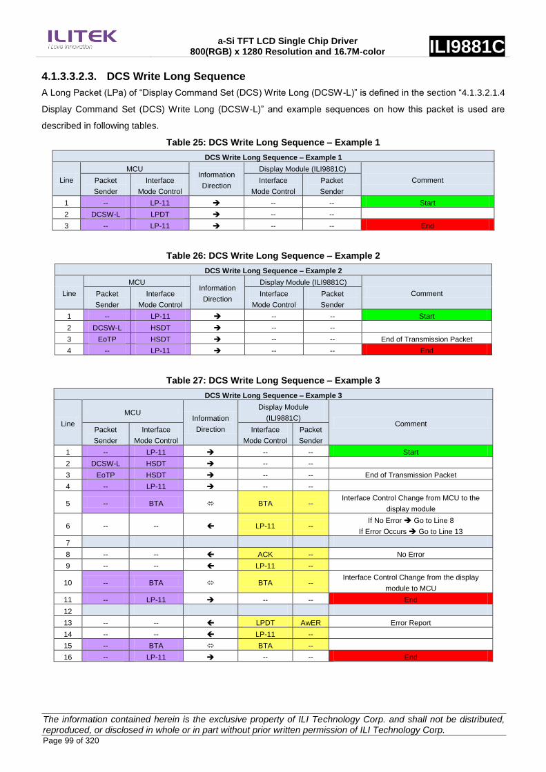
a-Si TFT LCD Single Chip Driver 800(RGB) x 1280 Resolution and 16.7M-color ILI9881C
The information contained herein is the exclusive property of ILI Technology Corp. and shall not be distributed, reproduced, or disclosed in whole or in part without prior written permission of ILI Technology Corp. Page 99 of 320
4.1.3.3.2.3. DCS Write Long Sequence
A Long Packet (LPa) of “Display Command Set (DCS) Write Long (DCSW-L)” is defined in the section “4.1.3.2.1.4
Display Command Set (DCS) Write Long (DCSW-L)” and example sequences on how this packet is used are
described in following tables.
Table 25: DCS Write Long Sequence – Example 1
DCS Write Long Sequence – Example 1
Line
MCU Information
Direction
Display Module (ILI9881C)
Comment Packet
Sender
Interface
Mode Control
Interface
Mode Control
Packet
Sender
1 -- LP-11 -- -- Start
2 DCSW-L LPDT -- --
3 -- LP-11 -- -- End
Table 26: DCS Write Long Sequence – Example 2
DCS Write Long Sequence – Example 2
Line
MCU Information
Direction
Display Module (ILI9881C)
Comment Packet
Sender
Interface
Mode Control
Interface
Mode Control
Packet
Sender
1 -- LP-11 -- -- Start
2 DCSW-L HSDT -- --
3 EoTP HSDT -- -- End of Transmission Packet
4 -- LP-11 -- -- End
Table 27: DCS Write Long Sequence – Example 3
DCS Write Long Sequence – Example 3
Line
MCU Information
Direction
Display Module
(ILI9881C) Comment
Packet
Sender
Interface
Mode Control
Interface
Mode Control
Packet
Sender
1 -- LP-11 -- -- Start
2 DCSW-L HSDT -- --
3 EoTP HSDT -- -- End of Transmission Packet
4 -- LP-11 -- --
5 -- BTA BTA -- Interface Control Change from MCU to the
display module
6 -- -- LP-11 -- If No Error Go to Line 8
If Error Occurs Go to Line 13
7
8 -- -- ACK -- No Error
9 -- -- LP-11 --
10 -- BTA BTA -- Interface Control Change from the display
module to MCU
11 -- LP-11 -- -- End
12
13 -- -- LPDT AwER Error Report
14 -- -- LP-11 --
15 -- BTA BTA --
16 -- LP-11 -- -- End

a-Si TFT LCD Single Chip Driver 800(RGB) x 1280 Resolution and 16.7M-color ILI9881C
The information contained herein is the exclusive property of ILI Technology Corp. and shall not be distributed, reproduced, or disclosed in whole or in part without prior written permission of ILI Technology Corp. Page 100 of 320
4.1.3.3.2.4. DCS Read, No Parameter Sequence
A Short Packet (SPa) of “Display Command Set (DCS) Read, No Parameter (DCSRN-S)” is defined in the section
“4.1.3.2.1.5 Display Command Set (DCS) Read, No Parameter (DCSRN-S)” and example sequences on how this
packet is used are described in following tables.
Table 28: DCS Read, No Parameter Sequence – Example 1
DCS Read, No Parameter Sequence – Example 1
Line
MCU Information
Direction
Display Module (ILI9881C)
Comment Packet
Sender
Interface
Mode Control
Interface
Mode Control
Packet
Sender
1 -- LP-11 -- -- Start
2 SMRPS-S HSDT -- -- Defined how many data byte is wanted to read :
1 byte
3 DCSRN-S HSDT -- -- Wanted to get a response ID1 (DAh)
4 EoTP HSDT -- -- End of Transmission Packet
5 -- LP-11 -- --
6 -- BTA BTA -- Interface Control Change from MCU to the display
module
7 -- -- LP-11 --
If No Error Go to Line 9
If Error Occurs Go to Line 14
If Error is Corrected by ECC Go to Line 19
8
9 -- -- LPDT DCSRR1-S Response 1 byte return
10 -- -- LP-11 --
11 -- BTA BTA -- Interface Control Change from the display module
to MCU
12 -- LP-11 -- -- End
13
14 -- -- LPDT AwER Error Report
15 -- -- LP-11 --
16 -- BTA BTA -- Interface Control Change from the display module
to MCU
17 -- LP-11 -- -- End
18
19 -- -- LPDT DCSRR1-S Response 1 byte return
20 -- -- LPDT AwER Error Report (Error is corrected by ECC)
21 LP-11 --
22 -- BTA BTA -- Interface Control Change from the display module
to MCU
23 -- LP-11 -- -- End
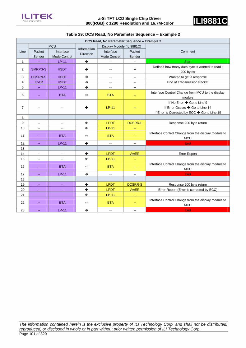
a-Si TFT LCD Single Chip Driver 800(RGB) x 1280 Resolution and 16.7M-color ILI9881C
The information contained herein is the exclusive property of ILI Technology Corp. and shall not be distributed, reproduced, or disclosed in whole or in part without prior written permission of ILI Technology Corp. Page 101 of 320
Table 29: DCS Read, No Parameter Sequence – Example 2
DCS Read, No Parameter Sequence – Example 2
Line
MCU Information
Direction
Display Module (ILI9881C)
Comment Packet
Sender
Interface
Mode Control
Interface
Mode Control
Packet
Sender
1 -- LP-11 -- -- Start
2 SMRPS-S HSDT -- -- Defined how many data byte is wanted to read :
200 bytes
3 DCSRN-S HSDT -- -- Wanted to get a response
4 EoTP HSDT -- -- End of Transmission Packet
5 -- LP-11 -- --
6 -- BTA BTA -- Interface Control Change from MCU to the display
module
7 -- -- LP-11 --
If No Error Go to Line 9
If Error Occurs Go to Line 14
If Error is Corrected by ECC Go to Line 19
8
9 -- -- LPDT DCSRR-L Response 200 byte return
10 -- -- LP-11 --
11 -- BTA BTA -- Interface Control Change from the display module to
MCU
12 -- LP-11 -- -- End
13
14 -- -- LPDT AwER Error Report
15 -- -- LP-11 --
16 -- BTA BTA -- Interface Control Change from the display module to
MCU
17 -- LP-11 -- -- End
18
19 -- -- LPDT DCSRR-S Response 200 byte return
20 -- -- LPDT AwER Error Report (Error is corrected by ECC)
21 LP-11 --
22 -- BTA BTA -- Interface Control Change from the display module to
MCU
23 -- LP-11 -- -- End

a-Si TFT LCD Single Chip Driver 800(RGB) x 1280 Resolution and 16.7M-color ILI9881C
The information contained herein is the exclusive property of ILI Technology Corp. and shall not be distributed, reproduced, or disclosed in whole or in part without prior written permission of ILI Technology Corp. Page 102 of 320
4.1.3.3.2.5. Null Packet, No Data Sequence
A Long Packet (LPa) of “Null Packet, No Data (NP-L)” is defined in the section “4.1.3.2.1.6 Null Packet, No Data
(NP-L)”, and an example sequence on how this packet is used is described in the following table.
Table 30: Null Packet, No Data Sequence - Example
Null Packet, No Data Sequence – Example
Line
MCU Information
Direction
Display Module (ILI9881C)
Comment Packet
Sender
Interface
Mode Control
Interface
Mode Control
Packet
Sender
1 -- LP-11 -- -- Start
2 NP-L HSDT -- -- Only High Speed Data Transmission is used
3 EoTP HSDT -- -- End of Transmission Packet
4 -- LP-11 -- -- End
4.1.3.3.2.6. End of Transmission Packet
A Short Packet (SPa) of “End of Transmission (EoTP)” is defined in the section “4.1.3.2.1.7 End of Transmission
Packet (EoTP)”, and an example sequence on how this packet is used is described in the following table.
Table 31: End of Transmission Packet – Example
End of Transmission Packet – Example
Line
MCU Information
Direction
Display Module (ILI9881C)
Comment Packet
Sender
Interface
Mode Control
Interface
Mode Control
Packet
Sender
1 -- LP-11 -- -- Start
2 NP-L HSDT -- -- Only High Speed Data Transmission is used
3 EoTP HSDT -- -- End of Transmission Packet
4 -- LP-11 -- -- End
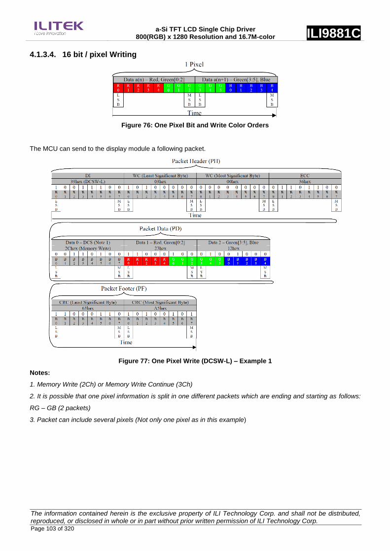
a-Si TFT LCD Single Chip Driver 800(RGB) x 1280 Resolution and 16.7M-color ILI9881C
The information contained herein is the exclusive property of ILI Technology Corp. and shall not be distributed, reproduced, or disclosed in whole or in part without prior written permission of ILI Technology Corp. Page 103 of 320
4.1.3.4. 16 bit / pixel Writing
Figure 76: One Pixel Bit and Write Color Orders
The MCU can send to the display module a following packet.
Figure 77: One Pixel Write (DCSW-L) – Example 1
Notes:
1. Memory Write (2Ch) or Memory Write Continue (3Ch)
2. It is possible that one pixel information is split in one different packets which are ending and starting as follows:
RG – GB (2 packets)
3. Packet can include several pixels (Not only one pixel as in this example)

a-Si TFT LCD Single Chip Driver 800(RGB) x 1280 Resolution and 16.7M-color ILI9881C
The information contained herein is the exclusive property of ILI Technology Corp. and shall not be distributed, reproduced, or disclosed in whole or in part without prior written permission of ILI Technology Corp. Page 104 of 320
Figure 78: Red / Green [0:2] Subpixel Write (DCSW1-S) – Example 2
Note: DCS (Data 0) can also be “Memory Write” (2Ch) command
Figure 79: Green [3:5] / Blue Subpixel Write (DCSW1-S) – Example 3
Notes:
1. DCS (Data 0) cannot be “Memory Write” (2Ch) command. It must always be “Memory Write Continue” (3Ch)
2. Previous data byte was R[0:4]G[0:2]

a-Si TFT LCD Single Chip Driver 800(RGB) x 1280 Resolution and 16.7M-color ILI9881C
The information contained herein is the exclusive property of ILI Technology Corp. and shall not be distributed, reproduced, or disclosed in whole or in part without prior written permission of ILI Technology Corp. Page 105 of 320
4.1.3.5. 24 bit/pixel Writing
Figure 80: One Pixel Bit and Color Write Orders
The MCU can send to the display module a following packet.
Figure 81: One Pixel Write (DCSW-L) – Example
Notes:
1. Memory Write (2Ch) or Memory Write Continue (3Ch)
2. It is possible that one pixel information is split in two or three different packets which are ending and
starting as follows:
• R – GB (2 packets)
• RG – B (2 packets)
• R – G – B (3 packets)
3. Packet can include several pixels (Not only one pixel as in this example)

a-Si TFT LCD Single Chip Driver 800(RGB) x 1280 Resolution and 16.7M-color ILI9881C
The information contained herein is the exclusive property of ILI Technology Corp. and shall not be distributed, reproduced, or disclosed in whole or in part without prior written permission of ILI Technology Corp. Page 106 of 320
Figure 82: Blue Subpixel Write (DCSW1-S) – Example 2
Notes:
1. DCS (Data 0) cannot be “Memory Write” (2Ch) command. It must always be “Memory Write Continue” (3Ch)
2. Previous data byte was G[0:7]
Figure 83: Green Subpixel Write (DCSW1-S) – Example 3
Notes:
1. DCS (Data 0) cannot be “Memory Write” (2Ch) command. It must always be “Memory Write Continue” (3Ch)
2. Previous data byte was R[0:7]
Figure 84: Red Subpixel Write (DCSW1-S) – Example 4
Notes:
1. DCS (Data 0) can also be “Memory Write Continue” (3Ch) command
2. Previous data byte was B[0:7]

a-Si TFT LCD Single Chip Driver 800(RGB) x 1280 Resolution and 16.7M-color ILI9881C
The information contained herein is the exclusive property of ILI Technology Corp. and shall not be distributed, reproduced, or disclosed in whole or in part without prior written permission of ILI Technology Corp. Page 107 of 320
4.2. Display Data Format
4.2.1. DSI Transmission Data Format
4.2.1.1. 16-bit per Pixel, Long Packet, Data Type 00 1110 (0Eh)
Packed Pixel Stream 16-Bit Format is a Long Packet used to transmit image data formatted as 16-bit pixels to a
Video Mode display module. The packet consists of the DI byte, a two-byte WC, an ECC byte, a payload of length
WC bytes and a two-byte checksum. Pixel format is red (5 bits), green (6 bits), and blue (5 bits), in that order. Note
that the Green component is split across two bytes. Within a color component, the LSB is sent first, the MSB last.
With this format, pixel boundaries align with byte boundaries every two bytes. The total line width (displayed plus
non-displayed pixels) should be a multiple of two bytes.
Normally, the ILI9881C has no frame buffer of its own, so all image data shall be supplied by the host processor at
a sufficiently high rate to avoid flicker or other visible artifice.
Figure 85: 16-bit per Pixel, Data Type 00 1110 (0Eh)
4.2.1.2. 18-bit per Pixel, Long Packet, Data Type = 01 1110 (1Eh)
Packed Pixel Stream 18-Bit Format (Packed) is a Long packet. It is used to transmit RGB image data formatted as
pixels to a Video Mode display module that displays 18-bit pixels. The packet consists of the DI byte, a two-byte
WC, an ECC byte, a payload of length WC bytes, and a two-byte Checksum. Pixel format is red (6 bits), green (6
bits) and blue (6 bits), in that order. Within a color component, the LSB is sent first, the MSB last.
Note that pixel boundaries only align with byte boundaries every four pixels (nine bytes). Preferably, display
modules employing this format have a horizontal extent (width in pixels) evenly divisible by four, so no partial bytes
remain at the end of the display line data. If the active (displayed) horizontal width is not a multiple of four pixels,
the transmitter shall send additional filled pixels at the end of the display line to make the transmitted width a

a-Si TFT LCD Single Chip Driver 800(RGB) x 1280 Resolution and 16.7M-color ILI9881C
The information contained herein is the exclusive property of ILI Technology Corp. and shall not be distributed, reproduced, or disclosed in whole or in part without prior written permission of ILI Technology Corp. Page 108 of 320
multiple of four pixels. The receiving peripheral shall not display the filled pixels when refreshing the display device.
For example, if a display device has an active display width of 399 pixels, the transmitter should send 400 pixels in
one or more packets. The receiver should display the first 399 pixels and discard the last pixel of the transmission.
With this format, the total line width (displayed and non-displayed pixels) should be a multiple of four pixels (nine
bytes).
Figure 86: 18-bit per Pixel, Data Type = 01 1110 (1Eh)
4.2.1.3. 18-bit per Pixel, Long Packet, Data Type = 10 1110 (2Eh)
In the 18-bit Pixel Loosely Packed format, each R, G, or B color component is six bits but is shifted to the upper bits
of the byte, such that the valid pixel bits occupy bits [7:2] of each byte. Bits [1:0] of each payload byte representing
active pixels are ignored. As a result, each pixel requires three bytes as it is transmitted across the link. This
requires more bandwidth than the “packed” format, but requires less shifting and multiplexing logic in the packing
and unpacking functions on each end of the Link.
This format is used to transmit RGB image data formatted as pixels to a Video Mode display module that displays
18-bit pixels. The packet consists of the DI byte, a two-byte WC, an ECC byte, a payload of length WC bytes and a
two-byte Checksum. The pixel format is red (6 bits), green (6 bits) and blue (6 bits) in that order. Within a color
component, the LSB is sent first, the MSB last.
With this format, pixel boundaries align with byte boundaries every three bytes. The total line width (displayed and
non-displayed pixels) should be a multiple of three bytes.
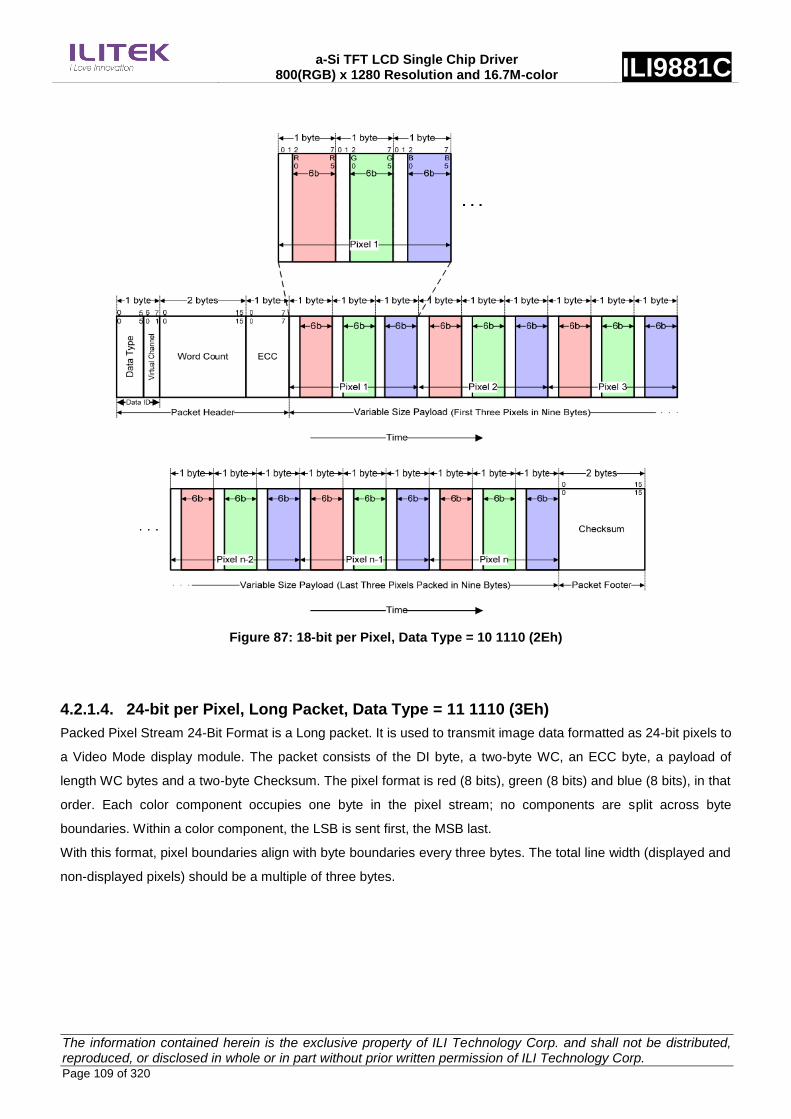
a-Si TFT LCD Single Chip Driver 800(RGB) x 1280 Resolution and 16.7M-color ILI9881C
The information contained herein is the exclusive property of ILI Technology Corp. and shall not be distributed, reproduced, or disclosed in whole or in part without prior written permission of ILI Technology Corp. Page 109 of 320
Figure 87: 18-bit per Pixel, Data Type = 10 1110 (2Eh)
4.2.1.4. 24-bit per Pixel, Long Packet, Data Type = 11 1110 (3Eh)
Packed Pixel Stream 24-Bit Format is a Long packet. It is used to transmit image data formatted as 24-bit pixels to
a Video Mode display module. The packet consists of the DI byte, a two-byte WC, an ECC byte, a payload of
length WC bytes and a two-byte Checksum. The pixel format is red (8 bits), green (8 bits) and blue (8 bits), in that
order. Each color component occupies one byte in the pixel stream; no components are split across byte
boundaries. Within a color component, the LSB is sent first, the MSB last.
With this format, pixel boundaries align with byte boundaries every three bytes. The total line width (displayed and
non-displayed pixels) should be a multiple of three bytes.
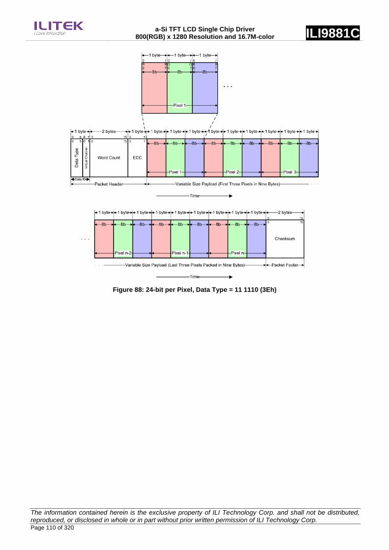
a-Si TFT LCD Single Chip Driver 800(RGB) x 1280 Resolution and 16.7M-color ILI9881C
The information contained herein is the exclusive property of ILI Technology Corp. and shall not be distributed, reproduced, or disclosed in whole or in part without prior written permission of ILI Technology Corp. Page 110 of 320
Figure 88: 24-bit per Pixel, Data Type = 11 1110 (3Eh)

a-Si TFT LCD Single Chip Driver 800(RGB) x 1280 Resolution and 16.7M-color ILI9881C
The information contained herein is the exclusive property of ILI Technology Corp. and shall not be distributed, reproduced, or disclosed in whole or in part without prior written permission of ILI Technology Corp. Page 111 of 320
4.2.2. 16/18-bit Color Data Mapping to 24-bit Pixel Data Operation
Table 32 below lists settings for 24-bit data mapping. Set the EPF[1:0] bits function, which defines three types of
data formats for 24-bit data (pixel data r, g, b) mapping.
Table 32: 16/18-bit Color Data Mapping to 24-bit Pixel Data Operation
EPF[1:0] Expand 16-bit color data (R,G,B) to
24-bit subpixel data (r, g, b)
Expand 18-bit color data (R,G,B) to
24-bit subpixel data (r, g, b)
00
0 is written to the LSB.
8 bits subpixel, data r [7:0] = {16-bit color data R [4:0], 3‟h0}
8 bits subpixel, data g [7:0] = {16-bit color data G [5:0], 2‟h0}
8 bits subpixel, data b [7:0] = {16-bit color data B [4:0], 3‟h0}
(Note3): that the data are converted as follows.
16-bit color data R [4:0] = 5‟h1F, G [5:0] = 6‟h3F, B [4:0] = 5‟h1F
→ 24-bit pixel data r, g, b [7:0] = 24‟hFFFFFF
0 is written to the LSB.
8 bits subpixel, data r [7:0] = {18-bit color data R [5:0], 2‟h0}
8 bits subpixel, data g [7:0] = {18-bit color data G [5:0], 2‟h0}
8 bits subpixel, data b [7:0] = {18-bit color data B [5:0], 2‟h0}
(Note1): that the data are converted as follows.
18-bit color data R [5:0] = 6‟h3F, G [5:0] = 6‟h3F ,B [5:0] = 6‟h3F
→ 24-bit pixel data r, g, b [7:0] = 24‟hFFFFFF
01
1 is written to the LSB.
8 bits subpixel, data r [7:0] = {16-bit color data R [4:0], 3‟h7}
8 bits subpixel, data g [7:0] = {16-bit color data G [5:0], 2‟h3}
8 bits subpixel, data b [7:0] = {16-bit color data B [4:0], 3‟h7}
(Note4): that the data are converted as follows.
16-bit color data R [4:0] = 5‟h0, G [5:0] = 6‟h0, B [4:0] = 5‟h0
→24-bit pixel data r, g, b [7:0] = 24‟h000000
1 is written to the LSB.
8 bits subpixel, data r [7:0] = {18-bit color data R [5:0], 2‟h3}
8 bits subpixel, data g [7:0] = {18-bit color data G [5:0], 2‟h3}
8 bits subpixel, data b [7:0] = {18-bit color data B [5:0], 2‟h3}
(Note2): that the data are converted as follows.
18-bit color data R [5:0] = 6‟h0, G [5:0] = 6‟h0, B [5:0] = 6‟h0
→24-bit pixel data r, g, b [7:0] = 24‟h000000
10
The MSB value is written to the LSB.
8 bits subpixel, data r [7:0] = {16-bit color data R [4:0], R [4:2]}
8 bits subpixel, data g [7:0] = {16-bit color data G [5:0], G [5:4]}
8 bits subpixel, data b [7:0] = {16-bit color data B [4:0], B [4:2]}
The MSB value is written to the LSB.
8 bits subpixel, data r [7:0] = {18-bit color data R [5:0], R [5:4]}
8 bits subpixel, data g [7:0] = {18-bit color data G [5:0], G [5:4]}
8 bits subpixel, data b [7:0] = {18-bit color data B [5:0], B [5:4]}
11 Same as setting “EPF [1:0] = 10” Same as setting “EPF [1:0] = 10”

a-Si TFT LCD Single Chip Driver 800(RGB) x 1280 Resolution and 16.7M-color ILI9881C
The information contained herein is the exclusive property of ILI Technology Corp. and shall not be distributed, reproduced, or disclosed in whole or in part without prior written permission of ILI Technology Corp. Page 112 of 320
Example1: 16-bit data mapping to 24-bit, EPF[1:0] = 10
R5 R4 R3 R2 R1 R0 G5 G4 G3 G2 G1 G0 B5 B4 B3 B2 B1 B0
Display Data 24-Bit Display Data
B6B7G6G7R6R7
R4 R3 R2 R1 R0 G5 G4 G3 G2 G1 G0 B4 B3 B2 B1 B0
16-Bit Input DataInput Data
Figure 89: EPF[1:0] = 10, 16-bit Data Mapping to 24-bit
Example2: 18-bit data mapping to 24-bit, EPF[1:0] = 10
R5 R4 R3 R2 R1 R0 G5 G4 G3 G2 G1 G0 B5 B4 B3 B2 B1 B0
Display Data 24-Bit Display Data
B6B7G6G7R6R7
R4 R3 R2 R1 R0 G5 G4 G3 G2 G1 G0 B4 B3 B2 B1 B0
18-Bit Input DataInput Data
B5R5
Figure 90: EPF[1:0] = 10, 18-bit Data Mapping to 24-bit
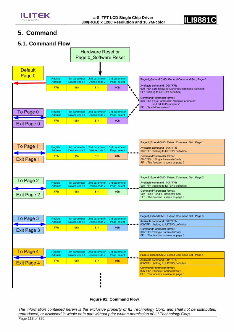
a-Si TFT LCD Single Chip Driver 800(RGB) x 1280 Resolution and 16.7M-color ILI9881C
The information contained herein is the exclusive property of ILI Technology Corp. and shall not be distributed, reproduced, or disclosed in whole or in part without prior written permission of ILI Technology Corp. Page 113 of 320
5. Command
5.1. Command Flow
Exit Page 3
To Page 2
Exit Page 2
To Page 1
Exit Page 1
Exit Page 0
To Page 0
To Page 4
To Page 3
Hardware Reset or
Page 0_Software Reset
Page 0_General CMD: General Command Set , Page 0
Default
Page 0
Exit Page 4
Page 1_Extend CMD: Extend Command Set , Page 1
Available command : 00h~FFh
00h~FFh : belong to ILITEK’s definition
Command/Parameter format:
00h~FEh : “Single Parameter”only
FFh : The function is same as page 0
Available command : 00h~FFh,
00h~FEh : are following General’s command definition,
FFh : belong to ILITEK’s definition
Command/Parameter format:
00h~FEh : “No Parameter”, “Single Parameter”
and “Multi-Parameters”
FFh : “Multi-Parameters”
Page 2_Extend CMD: Extend Command Set , Page 2
Available command : 00h~FFh
00h~FFh : belong to ILITEK’s definition
Page 3_Extend CMD: Extend Command Set , Page 3
Available command : 00h~FFh
00h~FFh : belong to ILITEK’s definition
Page 4_Extend CMD: Extend Command Set , Page 4
Available command : 00h~FFh
00h~FFh : belong to ILITEK’s definition
Command/Parameter format:
00h~FEh : “Single Parameter”only
FFh : The function is same as page 0
Command/Parameter format:
00h~FEh : “Single Parameter”only
FFh : The function is same as page 0
Command/Parameter format:
00h~FEh : “Single Parameter”only
FFh : The function is same as page 0
81h
Register
Address
1st parameter
Device code 1
2nd parameter
Device code 2
3rd parameter
Page_select
00h98hFFh
01h
02h
03h
04h
81h
Register
Address
1st parameter
Device code 1
2nd parameter
Device code 2
3rd parameter
Page_select
00h98hFFh
81h
Register
Address
1st parameter
Device code 1
2nd parameter
Device code 2
3rd parameter
Page_select
98hFFh
81h
Register
Address
1st parameter
Device code 1
2nd parameter
Device code 2
3rd parameter
Page_select
98hFFh
81h
Register
Address
1st parameter
Device code 1
2nd parameter
Device code 2
3rd parameter
Page_select
98hFFh
81h
Register
Address
1st parameter
Device code 1
2nd parameter
Device code 2
3rd parameter
Page_select
98hFFh
Figure 91: Command Flow
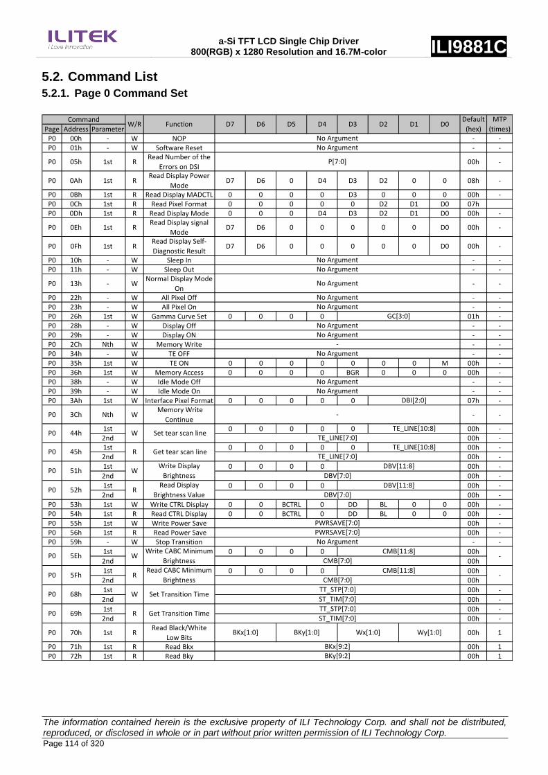
a-Si TFT LCD Single Chip Driver 800(RGB) x 1280 Resolution and 16.7M-color ILI9881C
The information contained herein is the exclusive property of ILI Technology Corp. and shall not be distributed, reproduced, or disclosed in whole or in part without prior written permission of ILI Technology Corp. Page 114 of 320
5.2. Command List
5.2.1. Page 0 Command Set
Page Address ParameterP0 00h - W NOP - -P0 01h - W Software Reset - -
P0 05h 1st RRead Number of the
Errors on DSI00h -
P0 0Ah 1st RRead Display Power
ModeD7 D6 0 D4 D3 D2 0 0 08h -
P0 0Bh 1st R Read Display MADCTL 0 0 0 0 D3 0 0 0 00h -P0 0Ch 1st R Read Pixel Format 0 0 0 0 0 D2 D1 D0 07hP0 0Dh 1st R Read Display Mode 0 0 0 D4 D3 D2 D1 D0 00h -
P0 0Eh 1st RRead Display signal
ModeD7 D6 0 0 0 0 0 D0 00h -
P0 0Fh 1st RRead Display Self-
Diagnostic ResultD7 D6 0 0 0 0 0 D0 00h -
P0 10h - W Sleep In - -P0 11h - W Sleep Out - -
P0 13h - WNormal Display Mode
On- -
P0 22h - W All Pixel Off - -P0 23h - W All Pixel On - -P0 26h 1st W Gamma Curve Set 0 0 0 0 01h -P0 28h - W Display Off - -P0 29h - W Display ON - -P0 2Ch Nth W Memory Write - -P0 34h - W TE OFF - -P0 35h 1st W TE ON 0 0 0 0 0 0 0 M 00h -P0 36h 1st W Memory Access 0 0 0 0 BGR 0 0 0 00h -P0 38h - W Idle Mode Off - -P0 39h - W Idle Mode On - -P0 3Ah 1st W Interface Pixel Format 0 0 0 0 0 07h -
P0 3Ch Nth W Memory Write
Continue- -
1st 0 0 0 0 0 00h -2nd 00h -1st 0 0 0 0 0 00h -2nd 00h -
1st 0 0 0 0 00h -
2nd 00h -
1st 0 0 0 0 00h -
2nd 00h -P0 53h 1st W Write CTRL Display 0 0 BCTRL 0 DD BL 0 0 00h -P0 54h 1st R Read CTRL Display 0 0 BCTRL 0 DD BL 0 0 00h -P0 55h 1st W Write Power Save 00h -P0 56h 1st R Read Power Save 00h -P0 59h - W Stop Transition - -
1st 0 0 0 0 00h
2nd 00h
1st 0 0 0 0 00h
2nd 00h
1st 00h -
2nd 00h -
1st 00h -
2nd 00h -
P0 70h 1st RRead Black/White
Low Bits00h 1
P0 71h 1st R Read Bkx 00h 1P0 72h 1st R Read Bky 00h 1
No Argument
DBI[2:0]
TE_LINE[7:0]
No Argument
-
CMB[7:0]
R
W -
-R
W
P0 69h Get Transition TimeTT_STP[7:0]
ST_TIM[7:0]
P0 5FhRead CABC Minimum
Brightness
CMB[11:8]
R
P0 68h Set Transition TimeST_TIM[7:0]
PWRSAVE[7:0]PWRSAVE[7:0]
P0
TE_LINE[7:0]
No Argument
TE_LINE[10:8]
52hRead Display
Brightness Value
DBV[11:8]
51hWrite Display
Brightness
DBV[11:8]
RP0
44h
45h
Set tear scan line
Get tear scan line
5EhWrite CABC Minimum
Brightness
P0
W
W
BKy[9:2]
Default
(hex)
CommandW/R Function D7 D6 D5
P0
P0
GC[3:0]No Argument
P[7:0]
No Argument
BKx[9:2]
No Argument
No Argument
No Argument
BKy[1:0]
CMB[11:8]
TT_STP[7:0]
MTP
(times)No ArgumentNo Argument
D4 D3 D2 D1 D0
-
TE_LINE[10:8]
No Argument
DBV[7:0]
DBV[7:0]
No Argument
BKx[1:0]
No Argument
Wx[1:0] Wy[1:0]
CMB[7:0]
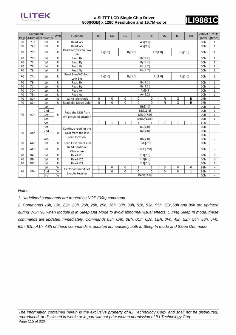
a-Si TFT LCD Single Chip Driver 800(RGB) x 1280 Resolution and 16.7M-color ILI9881C
The information contained herein is the exclusive property of ILI Technology Corp. and shall not be distributed, reproduced, or disclosed in whole or in part without prior written permission of ILI Technology Corp. Page 115 of 320
Page Address ParameterP0 73h 1st R Read Wx 00h 1P0 74h 1st R Read Wy 00h 1
P0 75h 1st RRead Red/Green Low
bits00h 1
P0 76h 1st R Read Rx 00h 1P0 77h 1st R Read Ry 00h 1P0 78h 1st R Read Gx 00h 1P0 79h 1st R Read Gy 00h 1
P0 7Ah 1st RRead Blue/AColour
Low Bits00h 1
P0 7Bh 1st R Read Bx 00h 1P0 7Ch 1st R Read By 00h 1P0 7Dh 1st R Read Ax 00h 1P0 7Eh 1st R Read Ay 00h 1P0 80h 1st W Write Idle Mode 0 0 0 0 0 R G B 07h -P0 81h 1st R Read Idle Mode Color 0 0 0 0 0 R G B 07h -
1st 00h 12nd 00h 13rd 00h 14th 00h 15th 1 1 1 1 1 1 1 1 FFh -1st 00h -2nd 00h -
: 00h -nth 00h -
P0 AAh 1st R Read First Checksum 00h -
P0 AFh 1st RRead Continue
Checksum00h -
P0 DAh 1st R Read ID1 00h 3P0 DBh 1st R Read ID2 00h 3P0 DCh 1st R Read ID3 00h 3
1st W 1 0 0 1 1 0 0 0 98h -2nd W 1 0 0 0 0 0 0 1 81h -3rd W 00h -
ID3[7:0]
P0 FFhEXTC Command Set
Enable RegisterPAGE[7:0]
P0 A8h R
Continue reading the
DDB from the last
read location
MRID[15:8]
D1[7:0]D2[7:0]
P0 A1h
:
Ax[1:0] Ay[1:0]
Rx[9:2]Ry[9:2]
Gy[9:2]
Bx[9:2]
D5MTP
(times)D4 D3 D2 D1 D0
Default
(hex)
Ry[1:0] Gx[1:0]
By[9:2]
CommandW/R Function D7 D6
Wy[9:2]Wx[9:2]
R Read the DDB from
the provided locationMRID[7:0]
Ax[9:2Ay[9:2]
Gy[1:0]
Gx[9:2]
Bx[1:0] By[1:0]
Rx[1:0]
FCS[7:0]
CCS[7:0]
ID2[6:0]
Dn[7:0]
ID1[7:0]
SID[7:0]SID[15:8]
Notes:
1. Undefined commands are treated as NOP (00h) command.
2. Commands 10h, 13h, 22h, 23h, 26h, 28h, 29h, 36h, 38h, 39h, 51h, 53h, 55h, 5Eh,68h and 80h are updated
during V-SYNC when Module is in Sleep Out Mode to avoid abnormal visual effects. During Sleep In mode, these
commands are updated immediately. Commands 05h, 0Ah, 0Bh, 0Ch, 0Dh, 0Eh, 0Fh, 45h, 52h, 54h, 56h, 5Fh,
69h, 81h, A1h, A8h of these commands is updated immediately both in Sleep In mode and Sleep Out mode.

a-Si TFT LCD Single Chip Driver 800(RGB) x 1280 Resolution and 16.7M-color ILI9881C
The information contained herein is the exclusive property of ILI Technology Corp. and shall not be distributed, reproduced, or disclosed in whole or in part without prior written permission of ILI Technology Corp. Page 116 of 320
5.2.2. Page 1 Command Set
Page Address ParameterP1 00h 1st R 98h -P1 01h 1st R 81h -P1 02h 1st R 00h -
P1 22h 1st W/R
Set Panel Operation
Mode and Data
Complement Setting
0 0BGR_PA
NEL
REV_PA
NEL
SS_PANE
L
GS_PAN
EL30h 1
P1 25h 1st W/R 14h -P1 26h 1st W/R 14h -P1 27h 1st W/R 05h -P1 28h 1st W/R 0 0 0 0 0 0 00h -P1 29h 1st W/R Touch 0 0 0 0 0 0 0 TOUCH_ 00h -
P1 2Eh 1st W/R Gate Number C8h 1
P1 31h 1st W/R Display Inversion 0 0 0 0 00h 1P1 34h 1st W/R Dithering Enable 0 0 0 0 0 0 0 DITH_EN 00h 1P1 40h 1st W/R 0 1 0 0 VCL_CLK VGHL_CL 33h 1P1 41h 1st W/R 0 0 33h 1P1 42h 1st W/R 0 0 44h 1P1 43h 1st W/R 0 0 55h 1P1 50h 1st W/R 95h 1P1 51h 1st W/R 95h 1P1 52h 1st W/R 0 0 0 0 0 0 0 VCM1[8] 00h 3P1 53h 1st W/R 7Bh 3P1 54h 1st W/R 0 0 0 0 0 0 0 VCM2[8] 00h 3P1 55h 1st W/R 7Bh 3P1 56h 1st W/R 0 0 0 NVM2 0 0 0 NVM1 00h -P1 58h 1st W/R Entry Mode Set LVD_EN 0 0 0 0 0 0 0 00h 1P1 60h 1st W/R 0 0 14h 1P1 61h 1st W/R 0 0 00h 1P1 62h 1st W/R 0 0 19h 1P1 63h 1st W/R 0 0 10h 1P1 A0h 1st W/R 0 0 00h 1P1 A1h 1st W/R 0 0Dh 1P1 A2h 1st W/R 0 1Dh 1P1 A3h 1st W/R 0 0 11h 1P1 A4h 1st W/R 0 0 0Ch 1P1 A5h 1st W/R 0 23h 1P1 A6h 1st W/R 0 0 17h 1P1 A7h 1st W/R 0 0 1Ch 1P1 A8h 1st W/R 82h 1P1 A9h 1st W/R 0 0 21h 1P1 AAh 1st W/R 0 0 2Ah 1P1 ABh 1st W/R 6Bh 1P1 ACh 1st W/R 0 0 19h 1P1 ADh 1st W/R 0 0 14h 1P1 AEh 1st W/R 0 45h 1P1 AFh 1st W/R 0 0 1Dh 1P1 B0h 1st W/R 0 0 23h 1P1 B1h 1st W/R 0 52h 1P1 B2h 1st W/R 0 63h 1P1 B3h 1st W/R 0 0 39h 1
P1 B6h 1st W/RIM_SW_
EN
RS_SW_
EN0 00h 1
P1 B7h 1st W/R 0 0 0 0 0 0LANSEL_
SW_EN
LANSEL_
SW00h 1
Read ID4ID4[7:0]
D5Command
W/R Function D7 D6 D1 D0MTP
(times)ID4[23:16]
Default
(hex)D4 D3 D2
ID4[15:8]
VP0[5:0]
SDT[5:0]CRT[5:0]
VREG1[7:0]
VBP[7:0]
EPF[1:0]
VCL_CLK_SELB[2:0]VGHL_CLK_SELA[2:0] VGHL_CLK_SELB[2:0]
Blanking Porch
Control
VFP[7:0]
HBP[7:0]HBP[9:8]
NL[7:0]
VP243[5:0]
VP144[5:0]
VP203[5:0]
VP16[5:0]
DINV[3:0]
4002_RATIO_FREQA[2:0] 4002_RATIO_FREQB[2:0]
Pump Clock
Adjustment
EXT_CPCK_SEL[1:0VCL_CLK_SELA[2:0]
VP255[5:0]
VCOM Control 1VCM1[7:0]
VCM2[7:0]
Source Timing Adjust
Pad ControlIM_SW[2:0] RS_SW[1:0]
Positive Gamma
Correction
VP4[6:0]
VP175[7:0]
VP239[5:0]
VP247[6:0]
Power Control 1VREG2[7:0]
VP80[7:0]VP111[5:0]
VP36[5:0]VP24[6:0]
VP251[6:0]
EQT[5:0]PCT[5:0]
VP8[6:0]
VP52[5:0]
VP12[5:0]
VP231[6:0]VP219[5:0]

a-Si TFT LCD Single Chip Driver 800(RGB) x 1280 Resolution and 16.7M-color ILI9881C
The information contained herein is the exclusive property of ILI Technology Corp. and shall not be distributed, reproduced, or disclosed in whole or in part without prior written permission of ILI Technology Corp. Page 117 of 320
Page Address ParameterP1 C0h 1st W/R 0 0 00h 1P1 C1h 1st W/R 0 0Dh 1P1 C2h 1st W/R 0 1Dh 1P1 C3h 1st W/R 0 0 11h 1P1 C4h 1st W/R 0 0 0Ch 1P1 C5h 1st W/R 0 23h 1P1 C6h 1st W/R 0 0 17h 1P1 C7h 1st W/R 0 0 1Ch 1P1 C8h 1st W/R 82h 1P1 C9h 1st W/R 0 0 21h 1P1 CAh 1st W/R 0 0 2Ah 1P1 CBh 1st W/R 6Bh 1P1 CCh 1st W/R 0 0 19h 1P1 CDh 1st W/R 0 0 14h 1P1 CEh 1st W/R 0 45h 1P1 CFh 1st W/R 0 0 1Dh 1P1 D0h 1st W/R 0 0 23h 1P1 D1h 1st W/R 0 52h 1P1 D2h 1st W/R 0 63h 1P1 D3h 1st W/R 0 0 39h 1P1 E0h 1st W/R 00h -P1 E1h 1st W/R 00h -P1 E2h 1st W/R 00h -P1 E3h 1st W/R 00h -P1 E4h 1st W/R 00h -P1 E5h 1st W/R 00h -P1 E6h 1st R 0 0 00h -P1 E7h 1st R 0 0 0 0 0 00h -
P1 E8h 1st RGAMMA
_P_MK
GAMMA
_N_MK00h -
P1 E9h 1st ROTP_BU
SY0 0 0 0 0 0 0 00h -
P1 F0h 1st W/R 00h 1P1 F1h 1st W/R 00h 1
1st W 1 0 0 1 1 0 0 0 98h -2nd W 1 0 0 0 0 0 0 1 81h -3rd W 01h -
P1 FFhEXTC Command Set
Enable RegisterPAGE[7:0]
NV Memory Status
Read
ID2_MK[2:0]
Time StampTime_Stamp_Week[7:0]Time_Stamp_Year[7:0]
NV Memory
Protection Key
KEY[23:16]KEY[15:8]KEY[7:0]
ID3_MK[2:0]
VCM2_MK[2:0] VCM1_MK[2:0]
ID1_MK[2:0]
VN243[5:0]VN247[6:0]VN251[6:0]
VN255[5:0]
NV Memory Write PGM_ADR[7:0]PGM_ADR[15:8]
PGM_DATA[7:0]
VN52[5:0]VN80[7:0]
VN175[7:0]VN203[5:0]
VN231[6:0]VN219[5:0]
VN239[5:0]
Negative Gamma
Correction
VN4[6:0]VN8[6:0]
VN111[5:0]VN144[5:0]
VN12[5:0]VN16[5:0]
VN24[6:0]VN36[5:0]
MTP
(times)
Default
(hex)VN0[5:0]
D5 D4 D3 D2 D0Command
W/R Function D7 D6 D1

a-Si TFT LCD Single Chip Driver 800(RGB) x 1280 Resolution and 16.7M-color ILI9881C
The information contained herein is the exclusive property of ILI Technology Corp. and shall not be distributed, reproduced, or disclosed in whole or in part without prior written permission of ILI Technology Corp. Page 118 of 320
5.2.3. Page 2 Command Set
Page Address ParameterP2 03h 1st W/R 0 1 29h 1P2 04h 1st W/R 0 0 14h 1P2 05h 1st W/R 0 0 32h 1
P2 06h 1st W/R 0 0LEDPW
M_POL
LEDON_
POLLEDON 00h 1
P2 07h 1st W/R 0Eh 1P2 10h 1st W/R 0 0 0 AXIS_EN 0 PRT_EN SKIN_EN 0 06h 1
P2 11h 1st W/R 0AUTO_M
EAN0 0 CN_EN CN_INV SHP_EN 0 00h 1
P2 12h 1st W/R 0 0 0 0 0 0 02h 1P2 13h 1st W/R 0 0 0 0 20h 1P2 15h 1st W/R 80h 1
P2 16h 1st W/R
SRE_HYS
TERESIS_
EN
0 0SRE_DIM
_EN
SRE_SC_
EN
SRE_CE_
EN0 0 1Ch 1
P2 17h 1st W/R 0 0 01h 1P2 18h 1st W/R 08h 1P2 19h 1st W/R C0h 1P2 1Ah 1st W/R 0 0 07h 1P2 1Bh 1st W/R 0 0 09h 1P2 1Ch 1st W/R 0 0 0Ch 1P2 40h 1st W/R 0 0 0 02h 1P2 41h 1st W/R 0 0 0 04h 1P2 42h 1st W/R 0 0 0 06h 1P2 43h 1st W/R 0 0 0 08h 1P2 44h 1st W/R 0 0 0 0Ah 1P2 45h 1st W/R 0 0 0 0Ch 1P2 46h 1st W/R 0 0 0 0Eh 1P2 47h 1st W/R 0 0 0 0Eh 1P2 48h 1st W/R 0 0 0 0Ch 1P2 49h 1st W/R 0 0 0 0Ah 1P2 4Ah 1st W/R 0 0 0 08h 1P2 4Bh 1st W/R 0 0 0 06h 1P2 4Ch 1st W/R 0 0 0 04h 1P2 4Dh 1st W/R 0 0 0 03h 1P2 4Eh 1st W/R 0 0 0 02h 1P2 4Fh 1st W/R 0 0 0 00h 1P2 5Ah 1st W/R 0 0 0 18h 1P2 5Bh 1st W/R 64h 1P2 5Ch 1st W/R 1Eh 1P2 60h 1st W/R 0 0 0Eh 1P2 61h 1st W/R 0 0 18h 1P2 62h 1st W/R 0 0 24h 1P2 63h 1st W/R 0 0 28h 1P2 64h 1st W/R 0 0 24h 1P2 65h 1st W/R 0 0 18h 1P2 66h 1st W/R 0 0 0Eh 1
1st W 1 0 0 1 1 0 0 0 98h -2nd W 1 0 0 0 0 0 0 1 81h -3rd W 02h -
CommandW/R Function D7 D6 D5
MTP
(times)
Default
(hex)D4 D3 D2 D1 D0
P2 FFhEXTC Command Set
Enable RegisterPAGE[7:0]
IIE Saturation
Protection Control
LEVEL0_SR[4:0]LEVEL1_SR[4:0]LEVEL2_SR[4:0]LEVEL3_SR[4:0]
PWM_DIV[7:0]
SRE_SC_GAIN_ADJ[2:0] SRE_HYSTERESIS_LIMIT[4:0]IIE Saturation
Enhancement Control
1
SE_RATIO_L[5:0]SE_RATIO_M[5:0]SE_RATIO_H[5:0]
Dynamic Backlight
Control 2
PWM_DUTY_PRECISION[2:0]
IIE Function Control
Dynamic Backlight
Control 1
TT_STP_MED[2:0]ST_TIM_LOW[2:0]ST_TIM_HIGH[2:0]
TT_STP_LOW[2:0]TT_STP_HIGH[2:0]ST_TIM_MED[2:0]
CN_LV[1:0]SHP_LV[1:0] SRE_MIDIV_LV[1:0
RGB_MEAN[7:0]
SRE_OFFS[2:0] SRE_DIM_STP[2:0]SRE_DIM_FRAME[7:0]
LEVEL4_SR[4:0]LEVEL5_SR[4:0]LEVEL6_SR[4:0]LEVEL7_SR[4:0]LEVEL8_SR[4:0]LEVEL9_SR[4:0]
CN_02[5:0]CN_03[5:0]
LEVEL10_SR[4:0]LEVEL11_SR[4:0]LEVEL12_SR[4:0]LEVEL13_SR[4:0]LEVEL14_SR[4:0]LEVEL15_SR[4:0]
CN_04[5:0]CN_05[5:0]CN_06[5:0]
IIE Sharpness
Enhancement Control
SHP_RATIO[4:0]SHP_THR_H[7:0]SHP_THR_L[7:0]
IIE Contrast
Enhancement Control
CN_00[5:0]CN_01[5:0]

a-Si TFT LCD Single Chip Driver 800(RGB) x 1280 Resolution and 16.7M-color ILI9881C
The information contained herein is the exclusive property of ILI Technology Corp. and shall not be distributed, reproduced, or disclosed in whole or in part without prior written permission of ILI Technology Corp. Page 119 of 320
5.2.4. Page 3 Command Set
Page Address Parameter1st W 1 0 0 1 1 0 0 0 98h -2nd W 1 0 0 0 0 0 0 1 81h -3rd W 03h -
P3 FFhEXTC Command Set
Enable RegisterPAGE[7:0]
MTP
(times)
Default
(hex)D4 D3 D2 D1 D0
CommandW/R Function D7 D6 D5

a-Si TFT LCD Single Chip Driver 800(RGB) x 1280 Resolution and 16.7M-color ILI9881C
The information contained herein is the exclusive property of ILI Technology Corp. and shall not be distributed, reproduced, or disclosed in whole or in part without prior written permission of ILI Technology Corp. Page 120 of 320
5.2.5. Page 4 Command Set
Page Address Parameter
P4 00h 1st W/R DSI Lanes ControlMIPI_LA
NE_SEL0 0 0 0 0 0 0 80h 1
P4 27h 1st W/RHFP_HB
P_OPT
VS_PW_
OPT00h 1
P4 28h 1st W/R 05h 1P4 29h 1st W/R 19h 1
P4 2Ah 1st W/RVS_OUT
_EN
HS_OUT
_EN
VS_OUT
_POL
HS_OUT
_POL0 0 STB_EN 0 F0h 1
P4 2Dh 1st W/R FFh 1
P4 2Fh 1st W/R 0 0 0 0 0 FRM_EN 00h 1P4 69h 1st W/R Power Control 1 1 0 1 1 1 D7h -P4 6Ch 1st W/R VCORE Setting 0 0 0 1 15h 1
P4 6Eh 1st W/R Power Control 2 0DI_PWR
_REG6Ah 1
P4 6Fh 1st W/R Power Control 3VGLREG
_EN_GO
DI_CP_V
CL_REG_
SEL
34h 1
P4 8Bh 1st W/R VCOM Control 2 1 1 1 0DI_VCM
_SEL0_E0 1 1 E3h 1
P4 8Ch 1st W/R 0 03h 1P4 8Dh 1st W/R 0 14h 1
P4 BBh 1st W/R
EN_TEM
P_PROC
ESS
0 1Eh 1
P4 BCh 1st W/R 0 0 1Eh 1P4 BDh 1st W/R 0 0 1Eh 1P4 BEh 1st W/R 0 0 1Eh 1P4 BFh 1st W/R 4Ch 1P4 C0h 1st W/R 4Ch 1P4 C1h 1st W/R 4Ch 1P4 C2h 1st W/R 4Ch 1P4 C8h 1st W/R 00h -P4 C9h 1st W/R 00h -P4 CAh 1st W/R 00h -P4 CBh 1st W/R 00h -P4 CCh 1st W/R 00h 1P4 CDh 1st W/R 02h 1
P4 CEh 1st W/R EN_TSVCOM_C
[8]
VCOM_L
[8]
VCOM_
M[8]
VCOM_
H[8]1 0 0 04h 1
P4 D7h 1st W/R OTP Control 0 0 0OTP_PA
TH0 0 1C -
1st W 1 0 0 1 1 0 0 0 98h -2nd W 1 0 0 0 0 0 0 1 81h -3rd W 04h -
TS_DEBT_OPT[3:0] TS_HYST_OPT[3:0]
TS_CTRL
BIST Mode Function
Power Control 4
VCOM_M[7:0]VCOM_H[7:0]
PROG_SEL[1:0]
P4 FFhEXTC Command Set
Enable RegisterPAGE[7:0]
TOUCH_OPT[1:0] VSOD[1:0] HSOM[1:0]
VCOM_C[7:0]VCOM_L[7:0]
CP_VGH_TAP_L[5:0]CP_VGH_TAP_M[5:0]
CP_VGH_TAP_C[5:0]
FRM_CYC[1:0]
FRM_PT[7:0]
DI_VCOM_CP_VGLCLP[6:0]
CP_VCL_CLP_OPTION_PRE[2:0]
DI_CP_VGH_BH[2:0] DI_CP_VGL_BL[2:0]
DI_VCORE_SEL[3:0]
REG1_VRH_CP[5:0]
TS_TH0[7:0]TS_TH1[7:0]TS_TH2[7:0]TS_TH3[7:0]
TS_TH0[9:8] TS_TH1[9:8] TS_TH2[9:8] TS_TH3[9:8]
CP_VGH_TAP_H[5:0]
DI_VCOM_REG_VGLREG[6:0]
MTP
(times)
Touch
Synchronization
Timing Adjust
CommandW/R Function D7 D6
HSOD[7:0]HSOHW[7:0]
Default
(hex)D5 D4 D3 D2 D1 D0
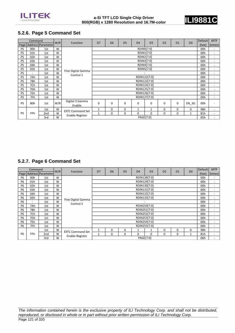
a-Si TFT LCD Single Chip Driver 800(RGB) x 1280 Resolution and 16.7M-color ILI9881C
The information contained herein is the exclusive property of ILI Technology Corp. and shall not be distributed, reproduced, or disclosed in whole or in part without prior written permission of ILI Technology Corp. Page 121 of 320
5.2.6. Page 5 Command Set
Page Address ParameterP5 00h 1st W 00h -P5 01h 1st W 00h -P5 02h 1st W 00h -P5 03h 1st W 00h -P5 04h 1st W 00h -P5 05h 1st W 00h -P5 : 1st W 00h -P5 7Ah 1st W 00h -P5 7Bh 1st W 00h -P5 7Ch 1st W 00h -P5 7Dh 1st W 00h -P5 7Eh 1st W 00h -P5 7Fh 1st W 00h -
P5 80h 1st W/RDigital 3 Gamma
Enable0 0 0 0 0 0 0 EN_3G 00h -
1st W 1 0 0 1 1 0 0 0 98h -2nd W 1 0 0 0 0 0 0 1 81h -3rd W 05h -
CommandW/R Function D7 D6 D5
MTP
(times)
Default
(hex)D4 D3 D2 D1 D0
P5 FFhEXTC Command Set
Enable RegisterPAGE[7:0]
Fine Digital Gamma
Control 1
RDIN0[7:0]RDIN1[7:0]RDIN2[7:0]
RDIN125[7:0]RDIN126[7:0]RDIN127[7:0]
RDIN3[7:0]RDIN4[7:0]RDIN5[7:0]
RDIN122[7:0]RDIN123[7:0]RDIN124[7:0]
:
5.2.7. Page 6 Command Set
Page Address ParameterP6 00h 1st W 00h -P6 01h 1st W 00h -P6 02h 1st W 00h -P6 03h 1st W 00h -P6 04h 1st W 00h -P6 05h 1st W 00h -P6 : 1st W 00h -P6 7Ah 1st W 00h -P6 7Bh 1st W 00h -P6 7Ch 1st W 00h -P6 7Dh 1st W 00h -P6 7Eh 1st W 00h -P6 7Fh 1st W 00h -
1st W 1 0 0 1 1 0 0 0 98h -2nd W 1 0 0 0 0 0 0 1 81h -3rd W 06h -
RDIN254[7:0]RDIN255[7:0]
RDIN132[7:0]RDIN133[7:0]
:RDIN250[7:0]RDIN251[7:0]RDIN252[7:0]
P6 FFhEXTC Command Set
Enable RegisterPAGE[7:0]
RDIN128[7:0]RDIN129[7:0]RDIN130[7:0]RDIN131[7:0]
Fine Digital Gamma
Control 2
RDIN253[7:0]
MTP
(times)
Default
(hex)D4 D3 D2 D1 D0
CommandW/R Function D7 D6 D5
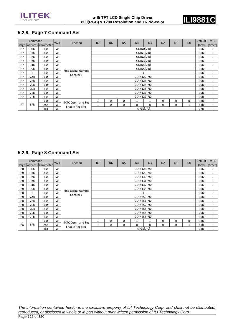
a-Si TFT LCD Single Chip Driver 800(RGB) x 1280 Resolution and 16.7M-color ILI9881C
The information contained herein is the exclusive property of ILI Technology Corp. and shall not be distributed, reproduced, or disclosed in whole or in part without prior written permission of ILI Technology Corp. Page 122 of 320
5.2.8. Page 7 Command Set
Page Address ParameterP7 00h 1st W 00h -P7 01h 1st W 00h -P7 02h 1st W 00h -P7 03h 1st W 00h -P7 04h 1st W 00h -P7 05h 1st W 00h -P7 : 1st W 00h -P7 7Ah 1st W 00h -P7 7Bh 1st W 00h -P7 7Ch 1st W 00h -P7 7Dh 1st W 00h -P7 7Eh 1st W 00h -P7 7Fh 1st W 00h -
1st W 1 0 0 1 1 0 0 0 98h -2nd W 1 0 0 0 0 0 0 1 81h -3rd W 07h -
CommandW/R Function D7 D6 D5
MTP
(times)
Default
(hex)D4 D3 D2 D1 D0
P7 FFhEXTC Command Set
Enable RegisterPAGE[7:0]
GDIN0[7:0]GDIN1[7:0]GDIN2[7:0]GDIN3[7:0]
Fine Digital Gamma
Control 3
GDIN125[7:0]GDIN126[7:0]GDIN127[7:0]
GDIN4[7:0]GDIN5[7:0]
:GDIN122[7:0]GDIN123[7:0]GDIN124[7:0]
5.2.9. Page 8 Command Set
Page Address ParameterP8 00h 1st W 00h -P8 01h 1st W 00h -P8 02h 1st W 00h -P8 03h 1st W 00h -P8 04h 1st W 00h -P8 05h 1st W 00h -P8 : 1st W 00h -P8 7Ah 1st W 00h -P8 7Bh 1st W 00h -P8 7Ch 1st W 00h -P8 7Dh 1st W 00h -P8 7Eh 1st W 00h -P8 7Fh 1st W 00h -
1st W 1 0 0 1 1 0 0 0 98h -2nd W 1 0 0 0 0 0 0 1 81h -3rd W 08h -
GDIN254[7:0]GDIN255[7:0]
GDIN128[7:0]GDIN129[7:0]GDIN130[7:0]GDIN131[7:0]GDIN132[7:0]GDIN133[7:0]
P8 FFhEXTC Command Set
Enable RegisterPAGE[7:0]
Fine Digital Gamma
Control 4:
GDIN250[7:0]GDIN251[7:0]GDIN252[7:0]GDIN253[7:0]
MTP
(times)
Default
(hex)D4 D3 D2 D1 D0
CommandW/R Function D7 D6 D5

a-Si TFT LCD Single Chip Driver 800(RGB) x 1280 Resolution and 16.7M-color ILI9881C
The information contained herein is the exclusive property of ILI Technology Corp. and shall not be distributed, reproduced, or disclosed in whole or in part without prior written permission of ILI Technology Corp. Page 123 of 320
5.2.10. Page 9 Command Set
Page Address ParameterP9 00h 1st W 00h -P9 01h 1st W 00h -P9 02h 1st W 00h -P9 03h 1st W 00h -P9 04h 1st W 00h -P9 05h 1st W 00h -P9 : 1st W 00h -P9 7Ah 1st W 00h -P9 7Bh 1st W 00h -P9 7Ch 1st W 00h -P9 7Dh 1st W 00h -P9 7Eh 1st W 00h -P9 7Fh 1st W 00h -
1st W 1 0 0 1 1 0 0 0 98h -2nd W 1 0 0 0 0 0 0 1 81h -3rd W 09h -
CommandW/R Function D7 D6 D5
MTP
(times)
Default
(hex)D4 D3 D2 D1 D0
P9 FFhEXTC Command Set
Enable RegisterPAGE[7:0]
BDIN0[7:0]BDIN1[7:0]BDIN2[7:0]BDIN3[7:0]
Fine Digital Gamma
Control 5
BDIN125[7:0]BDIN126[7:0]BDIN127[7:0]
BDIN4[7:0]BDIN5[7:0]
:BDIN122[7:0]BDIN123[7:0]BDIN124[7:0]
5.2.11. Page 10 Command Set
Page Address ParameterP10 00h 1st W 00h -P10 01h 1st W 00h -P10 02h 1st W 00h -P10 03h 1st W 00h -P10 04h 1st W 00h -P10 05h 1st W 00h -P10 : 1st W 00h -P10 7Ah 1st W 00h -P10 7Bh 1st W 00h -P10 7Ch 1st W 00h -P10 7Dh 1st W 00h -P10 7Eh 1st W 00h -P10 7Fh 1st W 00h -
1st W 1 0 0 1 1 0 0 0 98h -2nd W 1 0 0 0 0 0 0 1 81h -3rd W 0Ah -
BDIN254[7:0]BDIN255[7:0]
BDIN128[7:0]BDIN129[7:0]BDIN130[7:0]BDIN131[7:0]BDIN132[7:0]BDIN133[7:0]
P10 FFhEXTC Command Set
Enable RegisterPAGE[7:0]
Fine Digital Gamma
Control 6:
BDIN250[7:0]BDIN251[7:0]BDIN252[7:0]BDIN253[7:0]
MTP
(times)
Default
(hex)D4 D3 D2 D1 D0
CommandW/R Function D7 D6 D5

a-Si TFT LCD Single Chip Driver 800(RGB) x 1280 Resolution and 16.7M-color ILI9881C
The information contained herein is the exclusive property of ILI Technology Corp. and shall not be distributed, reproduced, or disclosed in whole or in part without prior written permission of ILI Technology Corp. Page 124 of 320
5.3. Page 0 Command Description
5.3.1. NOP (00h)
Command Page Page 0
Address Parameter W/R D7 D6 D5 D4 D3 D2 D1 D0 Default
00h - W No Argument -
Description
00h: NOP (No Operation).
This command is an empty command. It does not have any effect on the ILI9881C.
However, it can be used to terminate Memory Write or Memory Write Continue as described in RAMWR (Memory
Write) and RAMWRC (Memory Write Continue) Commands.
Restriction None
Register
Availability
Status Availability
Normal Mode On, Idle Mode Off, Sleep Out Yes
Normal Mode On, Idle Mode On, Sleep Out Yes
Sleep In Yes
Default
Status Default Value
Power On Sequence N/A
S/W Reset N/A
H/W Reset N/A
Flow Chart

a-Si TFT LCD Single Chip Driver 800(RGB) x 1280 Resolution and 16.7M-color ILI9881C
The information contained herein is the exclusive property of ILI Technology Corp. and shall not be distributed, reproduced, or disclosed in whole or in part without prior written permission of ILI Technology Corp. Page 125 of 320
5.3.2. Software Reset (01h)
Command Page Page 0
Address Parameter W/R D7 D6 D5 D4 D3 D2 D1 D0 Default
01h - W No Argument -
Description
01h: SWRESET (Software Reset).
When the Software Reset command is written, it causes software reset. It resets the commands and parameters to
their S/W Reset default values. (See default tables in each command description.)
The display is blank immediately.
Note: The Frame Memory content is kept or not by this command
Restriction
It is necessary to wait 5msec before sending a new command after software reset. The display module loads all factory
default values of the display supplier to the registers during this 5msec. If Software Reset is applied during the Sleep
Out mode, it will be necessary to wait 120msec for Sleep In sequence before sending the Sleep Out command.
The Software Reset Command cannot be sent during the Sleep Out sequence.
Register
Availability
Status Availability
Normal Mode On, Idle Mode Off, Sleep Out Yes
Normal Mode On, Idle Mode On, Sleep Out Yes
Sleep In Yes
Default
Status Default Value
Power On Sequence N/A
S/W Reset N/A
H/W Reset N/A
Flow Chart

a-Si TFT LCD Single Chip Driver 800(RGB) x 1280 Resolution and 16.7M-color ILI9881C
The information contained herein is the exclusive property of ILI Technology Corp. and shall not be distributed, reproduced, or disclosed in whole or in part without prior written permission of ILI Technology Corp. Page 126 of 320
5.3.3. Read Number of the Errors on DSI (05h)
Command Page Page 0
Address Parameter W/R D7 D6 D5 D4 D3 D2 D1 D0 Default
05h 1st R P[7:0] 00h
Description
05h: RDNUMED (Read Number of the Errors on DSI).
The parameter indicates the amount of errors on the DSI. The more detailed description of the bits is below.
P[6..0] bits indicate the amount of the error.
P[7] is set to 1 if there is overflow with P[6..0] bits.
P[7..0] bits are set to 0 (and RDDSM (0Eh)‟s D0 is set 0 at the same time) after the parameter information is sent (= the
read function is completed).
See also sections: “4.1.3.2.2.2 Acknowledge with Error Report (AwER)” and “5.3.8 Read Display Signal Mode (0Eh)”.
Restriction None
Register
Availability
Status Availability
Normal Mode On, Idle Mode Off, Sleep Out Yes
Normal Mode On, Idle Mode On, Sleep Out Yes
Sleep In Yes
Default
Status Default Value
Power On Sequence 00h
S/W Reset 00h
H/W Reset 00h
Flow Chart

a-Si TFT LCD Single Chip Driver 800(RGB) x 1280 Resolution and 16.7M-color ILI9881C
The information contained herein is the exclusive property of ILI Technology Corp. and shall not be distributed, reproduced, or disclosed in whole or in part without prior written permission of ILI Technology Corp. Page 127 of 320
5.3.4. Read Display Power Mode (0Ah)
Command Page Page 0
Address Parameter W/R D7 D6 D5 D4 D3 D2 D1 D0 Default
0Ah 1st R D7 D6 0 D4 D3 D2 0 0 08h
Description
0A: RDDPM (Read Display Power Mode).
This command indicates the current status of the display, as described in the table below.
Bit Description Value Status
D7 Booster Voltage Status 0 Booster Off or has a fault.
1 Booster On and working OK
D6 Idle Mode On/Off 0 Idle Mode Off
1 Idle Mode On
D4 Sleep In/Out 0 Sleep In Mode
1 Sleep Out Mode
D3 Display Normal Mode On/Off 0 Display Normal Mode Off
1 Display Normal Mode On
D2 Display On/Off 0 Display is Off
1 Display is On
Restriction None
Register
Availability
Status Availability
Normal Mode On, Idle Mode Off, Sleep Out Yes
Normal Mode On, Idle Mode On, Sleep Out Yes
Sleep In Yes
Default
Status Default Value
Power On Sequence 08h
S/W Reset 08h
H/W Reset 08h
Flow Chart

a-Si TFT LCD Single Chip Driver 800(RGB) x 1280 Resolution and 16.7M-color ILI9881C
The information contained herein is the exclusive property of ILI Technology Corp. and shall not be distributed, reproduced, or disclosed in whole or in part without prior written permission of ILI Technology Corp. Page 128 of 320
5.3.5. Read Display MADCTL (0Bh)
Command Page Page 0
Address Parameter W/R D7 D6 D5 D4 D3 D2 D1 D0 Default
0Bh 1st R 0 0 0 0 D3 0 0 0 00h
Description
0B: RDDMADCTL (Read Display MADCTL).
This command indicates the current status of the display, as described in the table below.
Bit Description Value Status
D3 RGB/BGR Order (RGB) 0 RGB (When MADCTL D3=‟0‟)
1 BGR (When MADCTL D3=‟1‟)
Note: For Bits D3 also refer to 5.3.21Memory Access Control (36h).
Restriction None
Register
Availability
Status Availability
Normal Mode On, Idle Mode Off, Sleep Out Yes
Normal Mode On, Idle Mode On, Sleep Out Yes
Sleep In Yes
Default
Status Default Value
Power On Sequence 00h
S/W Reset 00h
H/W Reset 00h
Flow Chart

a-Si TFT LCD Single Chip Driver 800(RGB) x 1280 Resolution and 16.7M-color ILI9881C
The information contained herein is the exclusive property of ILI Technology Corp. and shall not be distributed, reproduced, or disclosed in whole or in part without prior written permission of ILI Technology Corp. Page 129 of 320
5.3.6. Read Display Pixel Format (0Ch)
Command Page Page 0
Address Parameter W/R D7 D6 D5 D4 D3 D2 D1 D0 Default
0Ch 1st R 0 0 0 0 0 D[2:0] 07h
Description
0Ch: RDDCOLMOD (Read Display COLMOD).
This command indicates the current status of the display as described in the table below:
DBI[2:0] Interface Pixel Format
101 16 bit/pixel
110 18 bit/pixel
111 24 bit/pixel
Others Not defined
Note: For D[2:0] also refer to 5.3.24 Interface Pixel Format (3Ah).
Restriction None
Register
Availability
Status Availability
Normal Mode On, Idle Mode Off, Sleep Out Yes
Normal Mode On, Idle Mode On, Sleep Out Yes
Sleep In Yes
Default
Status Default Value
Power On Sequence 07h
S/W Reset 07h
H/W Reset 07h
Flow Chart
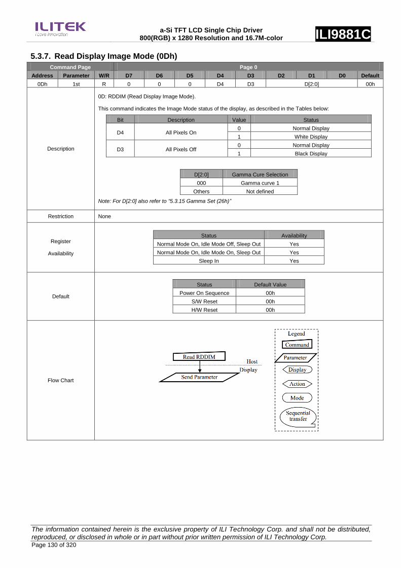
a-Si TFT LCD Single Chip Driver 800(RGB) x 1280 Resolution and 16.7M-color ILI9881C
The information contained herein is the exclusive property of ILI Technology Corp. and shall not be distributed, reproduced, or disclosed in whole or in part without prior written permission of ILI Technology Corp. Page 130 of 320
5.3.7. Read Display Image Mode (0Dh)
Command Page Page 0
Address Parameter W/R D7 D6 D5 D4 D3 D2 D1 D0 Default
0Dh 1st R 0 0 0 D4 D3 D[2:0] 00h
Description
0D: RDDIM (Read Display Image Mode).
This command indicates the Image Mode status of the display, as described in the Tables below:
Bit Description Value Status
D4 All Pixels On 0 Normal Display
1 White Display
D3 All Pixels Off 0 Normal Display
1 Black Display
D[2:0] Gamma Cure Selection
000 Gamma curve 1
Others Not defined
Note: For D[2:0] also refer to “5.3.15 Gamma Set (26h)”
Restriction None
Register
Availability
Status Availability
Normal Mode On, Idle Mode Off, Sleep Out Yes
Normal Mode On, Idle Mode On, Sleep Out Yes
Sleep In Yes
Default
Status Default Value
Power On Sequence 00h
S/W Reset 00h
H/W Reset 00h
Flow Chart
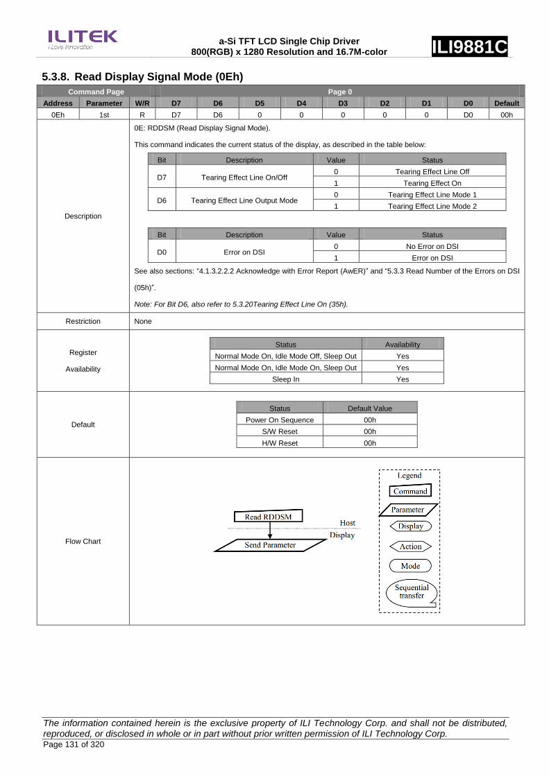
a-Si TFT LCD Single Chip Driver 800(RGB) x 1280 Resolution and 16.7M-color ILI9881C
The information contained herein is the exclusive property of ILI Technology Corp. and shall not be distributed, reproduced, or disclosed in whole or in part without prior written permission of ILI Technology Corp. Page 131 of 320
5.3.8. Read Display Signal Mode (0Eh)
Command Page Page 0
Address Parameter W/R D7 D6 D5 D4 D3 D2 D1 D0 Default
0Eh 1st R D7 D6 0 0 0 0 0 D0 00h
Description
0E: RDDSM (Read Display Signal Mode).
This command indicates the current status of the display, as described in the table below:
Bit Description Value Status
D7 Tearing Effect Line On/Off 0 Tearing Effect Line Off
1 Tearing Effect On
D6 Tearing Effect Line Output Mode 0 Tearing Effect Line Mode 1
1 Tearing Effect Line Mode 2
Bit Description Value Status
D0 Error on DSI 0 No Error on DSI
1 Error on DSI
See also sections: “4.1.3.2.2.2 Acknowledge with Error Report (AwER)” and “5.3.3 Read Number of the Errors on DSI
(05h)”.
Note: For Bit D6, also refer to 5.3.20Tearing Effect Line On (35h).
Restriction None
Register
Availability
Status Availability
Normal Mode On, Idle Mode Off, Sleep Out Yes
Normal Mode On, Idle Mode On, Sleep Out Yes
Sleep In Yes
Default
Status Default Value
Power On Sequence 00h
S/W Reset 00h
H/W Reset 00h
Flow Chart

a-Si TFT LCD Single Chip Driver 800(RGB) x 1280 Resolution and 16.7M-color ILI9881C
The information contained herein is the exclusive property of ILI Technology Corp. and shall not be distributed, reproduced, or disclosed in whole or in part without prior written permission of ILI Technology Corp. Page 132 of 320
5.3.9. Read Display Self-Diagnostic Result (0Fh)
Command Page Page 0
Address Parameter W/R D7 D6 D5 D4 D3 D2 D1 D0 Default
0Fh 1st R D7 D6 0 0 0 0 0 D0 00h
Description
0F: RDDSDR (Read Display Self-Diagnostic Result).
This command indicates the status of the display self-diagnostic results after the Sleep Out command, as described in
the table below:
Bit Description Action
D7 Register Loading Detection Invert the D7 bit when the EEPROM and register values are the same.
D6 Functionality Detection Invert the D6 bit when the chip meets user‟s functionality requirements.
D0 Checksums Comparison 0 = Checksums are the same
1 = Checksums are not the same
Restriction It will be necessary to wait 300ms after there is the last write access on Page 0 area registers before there can read Bit
D0 value.
Register
Availability
Status Availability
Normal Mode On, Idle Mode Off, Sleep Out Yes
Normal Mode On, Idle Mode On, Sleep Out Yes
Sleep In Yes
Default
Status Default Value
Power On Sequence 00h
S/W Reset 00h
H/W Reset 00h
Flow Chart

a-Si TFT LCD Single Chip Driver 800(RGB) x 1280 Resolution and 16.7M-color ILI9881C
The information contained herein is the exclusive property of ILI Technology Corp. and shall not be distributed, reproduced, or disclosed in whole or in part without prior written permission of ILI Technology Corp. Page 133 of 320
5.3.10. Sleep In (10h)
Command Page Page 0
Address Parameter W/R D7 D6 D5 D4 D3 D2 D1 D0 Default
10h - W No Argument -
Description
10h: SLPIN (Sleep In).
This command causes the ILI9881C to enter the minimum power consumption mode.
In this mode, the DC/DC converter, Internal oscillator, and panel scanning are all stopped.
Blank STOPOUT
MCU interface and memory are still working and the memory can keep its contents.
Ambient light based control is off.
Backlights and display are off.
Dimming function does not work when there is changing mode from Sleep Out to Sleep In.
Restriction
This command has no effect when the module is already in the Sleep In mode. To leave the Sleep In Mode, only the
Sleep Out Command (11h) is workable. It is necessary to wait 5msec before sending the next command; this is to allow
time for the supply voltages and clock circuits to become stable. It is necessary to wait 120msec after sending the
Sleep Out command (when in the Sleep In Mode) before the Sleep In command can be sent.
Register
Availability
Status Availability
Normal Mode On, Idle Mode Off, Sleep Out Yes
Normal Mode On, Idle Mode On, Sleep Out Yes
Sleep In Yes
Default
Status Default Value
Power On Sequence Sleep In Mode
S/W Reset Sleep In Mode
H/W Reset Sleep In Mode
Flow Chart
It takes 120msec to get into Sleep In mode after SLPIN command issued.
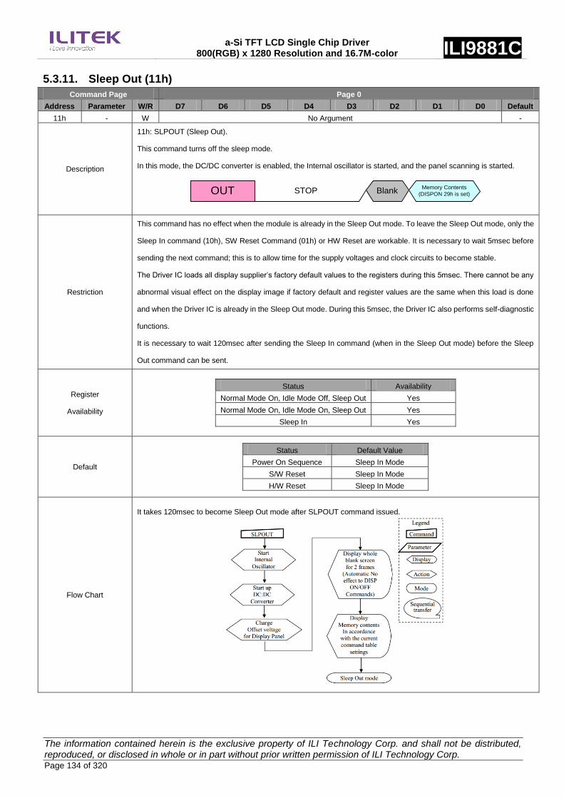
a-Si TFT LCD Single Chip Driver 800(RGB) x 1280 Resolution and 16.7M-color ILI9881C
The information contained herein is the exclusive property of ILI Technology Corp. and shall not be distributed, reproduced, or disclosed in whole or in part without prior written permission of ILI Technology Corp. Page 134 of 320
5.3.11. Sleep Out (11h)
Command Page Page 0
Address Parameter W/R D7 D6 D5 D4 D3 D2 D1 D0 Default
11h - W No Argument -
Description
11h: SLPOUT (Sleep Out).
This command turns off the sleep mode.
In this mode, the DC/DC converter is enabled, the Internal oscillator is started, and the panel scanning is started.
STOP BlankMemory Contents
(DISPON 29h is set)OUT
Restriction
This command has no effect when the module is already in the Sleep Out mode. To leave the Sleep Out mode, only the
Sleep In command (10h), SW Reset Command (01h) or HW Reset are workable. It is necessary to wait 5msec before
sending the next command; this is to allow time for the supply voltages and clock circuits to become stable.
The Driver IC loads all display supplier‟s factory default values to the registers during this 5msec. There cannot be any
abnormal visual effect on the display image if factory default and register values are the same when this load is done
and when the Driver IC is already in the Sleep Out mode. During this 5msec, the Driver IC also performs self-diagnostic
functions.
It is necessary to wait 120msec after sending the Sleep In command (when in the Sleep Out mode) before the Sleep
Out command can be sent.
Register
Availability
Status Availability
Normal Mode On, Idle Mode Off, Sleep Out Yes
Normal Mode On, Idle Mode On, Sleep Out Yes
Sleep In Yes
Default
Status Default Value
Power On Sequence Sleep In Mode
S/W Reset Sleep In Mode
H/W Reset Sleep In Mode
Flow Chart
It takes 120msec to become Sleep Out mode after SLPOUT command issued.

a-Si TFT LCD Single Chip Driver 800(RGB) x 1280 Resolution and 16.7M-color ILI9881C
The information contained herein is the exclusive property of ILI Technology Corp. and shall not be distributed, reproduced, or disclosed in whole or in part without prior written permission of ILI Technology Corp. Page 135 of 320
5.3.12. Normal Display Mode On (13h)
Command Page Page 0
Address Parameter W/R D7 D6 D5 D4 D3 D2 D1 D0 Default
13h - W No Argument -
Description 13h: NORON (Normal Display Mode On).
This command returns the display to normal mode.
Restriction This command has no effect when the Normal Display Mode is active.
Register
Availability
Status Availability
Normal Mode On, Idle Mode Off, Sleep Out Yes
Normal Mode On, Idle Mode On, Sleep Out Yes
Sleep In Yes
Default
Status Default Value
Power On Sequence Normal Display Mode On
S/W Reset Normal Display Mode On
H/W Reset Normal Display Mode On
Flow Chart

a-Si TFT LCD Single Chip Driver 800(RGB) x 1280 Resolution and 16.7M-color ILI9881C
The information contained herein is the exclusive property of ILI Technology Corp. and shall not be distributed, reproduced, or disclosed in whole or in part without prior written permission of ILI Technology Corp. Page 136 of 320
5.3.13. All Pixel Off (22h)
Command Page Page 0
Address Parameter W/R D7 D6 D5 D4 D3 D2 D1 D0 Default
22h - W No Argument -
Description
22h: ALLPOFF (All Pixels Off).
This command turns the display panel black in „Sleep Out‟ mode and a status bit of the „Read Display Image Mode‟
register (0Dh) can be read.
This command makes no change of contents of the input data (or frame memory). This command does not change any
other status.
Input Data/ Memory Display Panel
‘All Pixels On‟ or ‟Normal Display Mode On‟ commands are used to leave this mode. When ILI9881C works in ‟Idle
Mode On‟ and „Sleep Out‟ state, the display panel is showing the content of the frame memory after ‘Normal Display
Mode On‟ commands.
Restriction This command has no effect when module is already in all pixels off mode.
Register
Availability
Status Availability
Normal Mode On, Idle Mode Off, Sleep Out Yes
Normal Mode On, Idle Mode On, Sleep Out Yes
Sleep In Yes
Default
Status Default Value
Power On Sequence OFF
S/W Reset OFF
H/W Reset OFF
Flow Chart

a-Si TFT LCD Single Chip Driver 800(RGB) x 1280 Resolution and 16.7M-color ILI9881C
The information contained herein is the exclusive property of ILI Technology Corp. and shall not be distributed, reproduced, or disclosed in whole or in part without prior written permission of ILI Technology Corp. Page 137 of 320
5.3.14. All Pixel On (23h)
Command Page Page 0
Address Parameter W/R D7 D6 D5 D4 D3 D2 D1 D0 Default
23h - W No Argument -
Description
23h: ALLPON (All Pixels On).
This command turns the display panel white in „Sleep out„ mode and a status bit of the „Read Display Image Mode‟
register (0Dh) can be read.
This command makes no change of contents of the input data (or frame memory). This command does not change any
other status.
Input Data/ Memory Display Panel
‘All Pixels Off‟ or ‟Normal Display Mode On‟ commands are used to leave this mode.
When ILI9881C works in „Idle Mode On‟ and „Sleep Out‟ state, the display panel is showing the content of the frame
memory after ‘Normal Display Mode On‟ commands.
Restriction This command has no effect when module is already in all pixels on mode.
Register
Availability
Status Availability
Normal Mode On, Idle Mode Off, Sleep Out Yes
Normal Mode On, Idle Mode On, Sleep Out Yes
Sleep In Yes
Default
Status Default Value
Power On Sequence OFF
S/W Reset OFF
H/W Reset OFF
Flow Chart
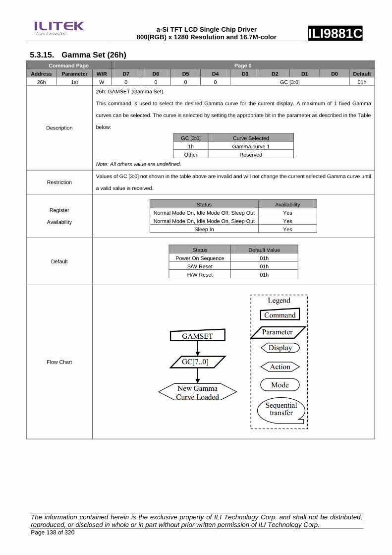
a-Si TFT LCD Single Chip Driver 800(RGB) x 1280 Resolution and 16.7M-color ILI9881C
The information contained herein is the exclusive property of ILI Technology Corp. and shall not be distributed, reproduced, or disclosed in whole or in part without prior written permission of ILI Technology Corp. Page 138 of 320
5.3.15. Gamma Set (26h)
Command Page Page 0
Address Parameter W/R D7 D6 D5 D4 D3 D2 D1 D0 Default
26h 1st W 0 0 0 0 GC [3:0] 01h
Description
26h: GAMSET (Gamma Set).
This command is used to select the desired Gamma curve for the current display. A maximum of 1 fixed Gamma
curves can be selected. The curve is selected by setting the appropriate bit in the parameter as described in the Table
below:
GC [3:0] Curve Selected
1h Gamma curve 1
Other Reserved
Note: All others value are undefined.
Restriction Values of GC [3:0] not shown in the table above are invalid and will not change the current selected Gamma curve until
a valid value is received.
Register
Availability
Status Availability
Normal Mode On, Idle Mode Off, Sleep Out Yes
Normal Mode On, Idle Mode On, Sleep Out Yes
Sleep In Yes
Default
Status Default Value
Power On Sequence 01h
S/W Reset 01h
H/W Reset 01h
Flow Chart

a-Si TFT LCD Single Chip Driver 800(RGB) x 1280 Resolution and 16.7M-color ILI9881C
The information contained herein is the exclusive property of ILI Technology Corp. and shall not be distributed, reproduced, or disclosed in whole or in part without prior written permission of ILI Technology Corp. Page 139 of 320
5.3.16. Display Off (28h)
Command Page Page 0
Address Parameter W/R D7 D6 D5 D4 D3 D2 D1 D0 Default
28h - W No Argument -
Description
28h: DISPOFF (Display Off)
This command is used to enter into the Display Off mode. Output from the input data (or frame memory) is disabled
and a blank page inserted. This command makes no change of contents of the input data (or frame memory) and does
not change any other status. There will be no abnormal visible effect on the display.
Input Data/ Memory Display Panel
Restriction This command has no effect when the module is already in the Display Off mode.
Register
Availability
Status Availability
Normal Mode On, Idle Mode Off, Sleep Out Yes
Normal Mode On, Idle Mode On, Sleep Out Yes
Sleep In Yes
Default
Status Default Value
Power On Sequence Display Off
S/W Reset Display Off
H/W Reset Display Off
Flow Chart

a-Si TFT LCD Single Chip Driver 800(RGB) x 1280 Resolution and 16.7M-color ILI9881C
The information contained herein is the exclusive property of ILI Technology Corp. and shall not be distributed, reproduced, or disclosed in whole or in part without prior written permission of ILI Technology Corp. Page 140 of 320
5.3.17. Display ON (29h)
Command Page Page 0
Address Parameter W/R D7 D6 D5 D4 D3 D2 D1 D0 Default
29h - W No Argument -
Description
29h: DISPON (Display On).
This command is used to recover from the Display Off mode. Output from the input data (or frame memory) is enabled.
This command makes no change of contents of the input data (or frame memory) and does not change any other
status.
Input Data/ Memory Display Panel
Restriction This command has no effect when the ILI9881C is already in the Display On mode.
Register
Availability
Status Availability
Normal Mode On, Idle Mode Off, Sleep Out Yes
Normal Mode On, Idle Mode On, Sleep Out Yes
Sleep In Yes
Default
Status Default Value
Power On Sequence Display Off
S/W Reset Display Off
H/W Reset Display Off
Flow Chart

a-Si TFT LCD Single Chip Driver 800(RGB) x 1280 Resolution and 16.7M-color ILI9881C
The information contained herein is the exclusive property of ILI Technology Corp. and shall not be distributed, reproduced, or disclosed in whole or in part without prior written permission of ILI Technology Corp. Page 141 of 320
5.3.18. Memory Write (2Ch)
Command Page Page 0
Address Parameter W/R D7 D6 D5 D4 D3 D2 D1 D0 Default
2Ch
1st W D1[23:16] 00~FFh
2nd W D1[15:8] 00~FFh
3rd W D1[7:0] 00~FFh
… W … 00~FFh
Nth W Dn[7:0] 00~FFh
Description
2Ch: RAMWR (Memory Write).
This command transfers data from the MCU to the Frame Memory. This command makes no change to the other
driver status. When this command is accepted, the column register and the page register are reset to zero.
Then D[23:0] is stored in the Frame Memory and the column register and the page register incremented at the same
time. Sending any other command can stop frame Write.
Restriction
This command‟s parameter length must be based on 2 pixel data length (6 bytes) (N=3 x n, N is multiple of 6).
When ILI9881C‟s work state is “Normal Mode On, Idle Mode On and Sleep Out”, full-resolution frame data must be
send by Memory Write (2Ch) and Memory Write Continue (3Ch) command.
Transmission sequences: LP_00 HS for R2Ch LP_00 HS for R3Ch LP_00 HS for CMD LP_00
Register
Availability
Status Availability
Normal Mode On, Idle Mode Off, Sleep Out Yes
Normal Mode On, Idle Mode On, Sleep Out Yes
Sleep In Yes
Default
Status Default Value
Power On Sequence Contents of memory is set randomly
S/W Reset Contents of memory is set randomly
H/W Reset Contents of memory is set randomly
Flow Chart

a-Si TFT LCD Single Chip Driver 800(RGB) x 1280 Resolution and 16.7M-color ILI9881C
The information contained herein is the exclusive property of ILI Technology Corp. and shall not be distributed, reproduced, or disclosed in whole or in part without prior written permission of ILI Technology Corp. Page 142 of 320
5.3.19. Tearing Effect Line Off (34h)
Command Page Page 0
Address Parameter W/R D7 D6 D5 D4 D3 D2 D1 D0 Default
34h - W No Argument -
Description 34h: TEOFF (Tearing Effect Line OFF).
This command is used to turn off the Display module’s Tearing Effect output signal from the TE signal line.
Restriction This command has no effect when the Tearing Effect output is already off.
Register
Availability
Status Availability
Normal Mode On, Idle Mode Off, Sleep Out Yes
Normal Mode On, Idle Mode On, Sleep Out Yes
Sleep In Yes
Default
Status Default Value
Power On Sequence Off
S/W Reset Off
H/W Reset Off
Flow Chart

a-Si TFT LCD Single Chip Driver 800(RGB) x 1280 Resolution and 16.7M-color ILI9881C
The information contained herein is the exclusive property of ILI Technology Corp. and shall not be distributed, reproduced, or disclosed in whole or in part without prior written permission of ILI Technology Corp. Page 143 of 320
5.3.20. Tearing Effect Line On (35h)
Command Page Page 0
Address Parameter W/R D7 D6 D5 D4 D3 D2 D1 D0 Default
35h 1st W 0 0 0 0 0 0 0 M 00
Description
35h: TEON (Tearing Effect Line ON).
This command is used to turn on the Tearing Effect output signal from the TE signal line. The Tearing Effect Line On
has one parameter which describes the mode of the Tearing Effect Output Line.
When M=0: The Tearing Effect Output line consists of V-Blanking information only:
TE
tvdl tvdhMode 1:
When M=1: The Tearing Effect Output Line consists of both V-Blanking and H-Blanking information:
thdl
TE
thdh
1st Line 1280th
Line
Invisible Line
Mode 2:
Note : The Tearing Effect Output line shall be low when the display module is in Sleep mode
Restriction This command has no effect when the Tearing Effect output is already ON.
Register
Availability
Status Availability
Normal Mode On, Idle Mode Off, Sleep Out Yes
Normal Mode On, Idle Mode On, Sleep Out Yes
Sleep In Yes
Default
Status Default Value
Power On Sequence Off
S/W Reset Off
H/W Reset Off

a-Si TFT LCD Single Chip Driver 800(RGB) x 1280 Resolution and 16.7M-color ILI9881C
The information contained herein is the exclusive property of ILI Technology Corp. and shall not be distributed, reproduced, or disclosed in whole or in part without prior written permission of ILI Technology Corp. Page 144 of 320
Flow Chart

a-Si TFT LCD Single Chip Driver 800(RGB) x 1280 Resolution and 16.7M-color ILI9881C
The information contained herein is the exclusive property of ILI Technology Corp. and shall not be distributed, reproduced, or disclosed in whole or in part without prior written permission of ILI Technology Corp. Page 145 of 320
5.3.21. Memory Access Control (36h)
Command Page Page 0
Address Parameter W/R D7 D6 D5 D4 D3 D2 D1 D0 Default
36h 1st W 0 0 0 0 BGR 0 0 0 00h
Description
36h: MADCTL (Memory Access Control).
This command makes no change on the other status of the driver.
Bit Symbol Name Description
D3 BGR RGB/BGR Order Color selector switch control
(0=RGB color filter panel, 1=BGR color filter panel)
R RG B G BDriver IC
SIG1 SIG2 SIG480
R G B
LCD Panel
SIG1 SIG2 SIG480
R G B
R G B
R G B
R G B
R G B
R RG B G BDriver IC
SIG1 SIG2 SIG480
RG B
LCD Panel
SIG1 SIG2 SIG480
RGB
R GB
RGB
RB G
RGB
BGR (RGB-BGR Order control bit)="0" BGR (RGB-BGR Order control bit)="1"
Restriction None
Register
Availability
Status Availability
Normal Mode On, Idle Mode Off, Sleep Out Yes
Normal Mode On, Idle Mode On, Sleep Out Yes
Sleep In Yes
Default
Status Default Value
Power On Sequence 00h
S/W Reset 00h
H/W Reset 00h
Flow Chart

a-Si TFT LCD Single Chip Driver 800(RGB) x 1280 Resolution and 16.7M-color ILI9881C
The information contained herein is the exclusive property of ILI Technology Corp. and shall not be distributed, reproduced, or disclosed in whole or in part without prior written permission of ILI Technology Corp. Page 146 of 320
5.3.22. Idle Mode Off (38h)
Command Page Page 0
Address Parameter W/R D7 D6 D5 D4 D3 D2 D1 D0 Default
38h - W No Argument -
Description
38h: IDMOFF (Idle mode off).
This command causes the Display module to exit the Idle mode.
In the Idle Mode Off, the display panel can display a maximum of 16.7M colors.
Restriction This command has no effect when the module is already in the Idle Mode Off.
Register
Availability
Status Availability
Normal Mode On, Idle Mode Off, Sleep Out Yes
Normal Mode On, Idle Mode On, Sleep Out Yes
Sleep In Yes
Default
Status Default Value
Power On Sequence Idle Mode Off
S/W Reset Idle Mode Off
H/W Reset Idle Mode Off
Flow Chart
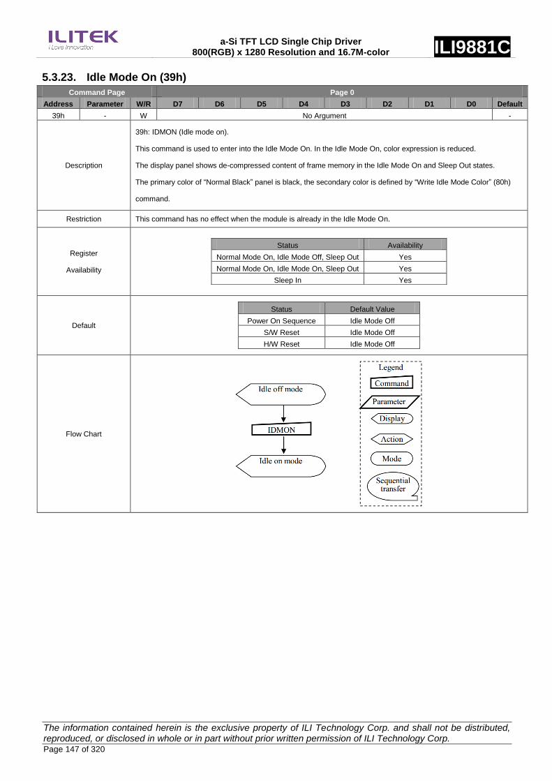
a-Si TFT LCD Single Chip Driver 800(RGB) x 1280 Resolution and 16.7M-color ILI9881C
The information contained herein is the exclusive property of ILI Technology Corp. and shall not be distributed, reproduced, or disclosed in whole or in part without prior written permission of ILI Technology Corp. Page 147 of 320
5.3.23. Idle Mode On (39h)
Command Page Page 0
Address Parameter W/R D7 D6 D5 D4 D3 D2 D1 D0 Default
39h - W No Argument -
Description
39h: IDMON (Idle mode on).
This command is used to enter into the Idle Mode On. In the Idle Mode On, color expression is reduced.
The display panel shows de-compressed content of frame memory in the Idle Mode On and Sleep Out states.
The primary color of “Normal Black” panel is black, the secondary color is defined by “Write Idle Mode Color” (80h)
command.
Restriction This command has no effect when the module is already in the Idle Mode On.
Register
Availability
Status Availability
Normal Mode On, Idle Mode Off, Sleep Out Yes
Normal Mode On, Idle Mode On, Sleep Out Yes
Sleep In Yes
Default
Status Default Value
Power On Sequence Idle Mode Off
S/W Reset Idle Mode Off
H/W Reset Idle Mode Off
Flow Chart

a-Si TFT LCD Single Chip Driver 800(RGB) x 1280 Resolution and 16.7M-color ILI9881C
The information contained herein is the exclusive property of ILI Technology Corp. and shall not be distributed, reproduced, or disclosed in whole or in part without prior written permission of ILI Technology Corp. Page 148 of 320
5.3.24. Interface Pixel Format (3Ah)
Command Page Page 0
Address Parameter W/R D7 D6 D5 D4 D3 D2 D1 D0 Default
3Ah 1st W 0 0 0 0 0 DBI[2:0] 07h
Description
3A: COLMOD (Interface Pixel Format).
This command is used to define the format of RGB picture data, which is to be transferred via the MIPI DSI Command
Mode. The formats are shown in the table:
Interface Format DBI[2:0]
Not Defined 000
Not Defined 001
Not Defined 010
Not Defined 011
Not Defined 100
16 bit/pixel 101
18 bit/pixel 110
24 bit/pixel 111
Restriction There is no visible effect until the Frame Memory is written to.
Register
Availability
Status Availability
Normal Mode On, Idle Mode Off, Sleep Out Yes
Normal Mode On, Idle Mode On, Sleep Out Yes
Sleep In Yes
Default
Status Default Value
Power On Sequence 07h
S/W Reset 07h
H/W Reset 07h
Flow Chart

a-Si TFT LCD Single Chip Driver 800(RGB) x 1280 Resolution and 16.7M-color ILI9881C
The information contained herein is the exclusive property of ILI Technology Corp. and shall not be distributed, reproduced, or disclosed in whole or in part without prior written permission of ILI Technology Corp. Page 149 of 320
5.3.25. Memory Write Continue (3Ch)
Command Page Page 0
Address Parameter W/R D7 D6 D5 D4 D3 D2 D1 D0 Default
3Ch
1st W D1[23:16] 00~FFh
2nd W D1[15:8] 00~FFh
3rd W D1[7:0] 00~FFh
… W … 00~FFh
Nth W Dn[7:0] 00~FFh
Description
3Ch: RAMWRC (Memory Write Continue).
This command is used to transfer data from the MCU to the Frame Memory, if want to continue the Frame Memory
write after the “Memory Write (2Ch)” command. This command makes no change to the status of the other driver.
When this command is accepted, the column register and the page register are not reset to zero since it has been
done on “Memory Write (2Ch)” command.
Sending any other command can stop frame Write.
Restriction This command‟s parameter length must be based on 2 pixel data length (6 bytes) (N=3 x n, N is multiple of 6).
Transmission sequences: LP_00 HS for R2Ch LP_00 HS for R3Ch LP_00 HS for CMD LP_00
Register
Availability
Status Availability
Normal Mode On, Idle Mode Off, Sleep Out Yes
Normal Mode On, Idle Mode On, Sleep Out Yes
Sleep In Yes
Default
Status Default Value
Power On Sequence Contents of memory is set randomly
S/W Reset Contents of memory is set randomly
H/W Reset Contents of memory is set randomly
Flow Chart

a-Si TFT LCD Single Chip Driver 800(RGB) x 1280 Resolution and 16.7M-color ILI9881C
The information contained herein is the exclusive property of ILI Technology Corp. and shall not be distributed, reproduced, or disclosed in whole or in part without prior written permission of ILI Technology Corp. Page 150 of 320
5.3.26. Set_Tear_Scanline (44h)
Command Page Page 0
Address Parameter W/R D7 D6 D5 D4 D3 D2 D1 D0 Default
44h 1st W 0 0 0 0 0 TE_LINE[10:8] 00h
2nd W TE_LINE[7:0] 00h
Description
44h: SET_TEAR_SCANLINE.
This command turns on the display module‟s Tearing Effect output signal on the TE signal line when the display
module reaches line N.
The Tearing Effect Line On has one parameter that describes the Tearing Effect Output Line mode. After issuing a
set_tear_scanline command to the display module, the Tearing Effect output signal, e.g. as in DBI-2 systems, shall be
a delayed version of V-Blanking information as illustrated by below figure.
In other words, the TE pulse width needs to be identical with normal mode Vsync related TE pulse.
TE
tvdl tvdh
Note that set_tear_scanline with N = 0 is equivalent to set_tear_on with M = 0.
The Tearing Effect Output line shall be active low when the display module is in Sleep mode.
Restriction
This command takes affect on the frame following the current frame.
Therefore, if the Tear Effect (TE) output is already ON, the TE output shall continue to operate as programmed by the
previous set_tear_on, or set_tear_scanline, command until the end of the frame.
Register
Availability
Status Availability
Normal Mode On, Idle Mode Off, Sleep Out Yes
Normal Mode On, Idle Mode On, Sleep Out Yes
Sleep In No
Default
Status Default Value
Power On Sequence N=0
S/W Reset N=0
H/W Reset N=0
Flow Chart

a-Si TFT LCD Single Chip Driver 800(RGB) x 1280 Resolution and 16.7M-color ILI9881C
The information contained herein is the exclusive property of ILI Technology Corp. and shall not be distributed, reproduced, or disclosed in whole or in part without prior written permission of ILI Technology Corp. Page 151 of 320
5.3.27. Get_Tear_Scanline (45h)
Command Page Page 0
Address Parameter W/R D7 D6 D5 D4 D3 D2 D1 D0 Default
45h 1st R 0 0 0 0 0 TE_LINE[10:8] 00h
2nd R TE_LINE[7:0] 00h
Description 45h: GET_TEAR_SCANLINE.
This command returns setting value of Set_Tear_Scanline command (44h).
Restriction None
Register
Availability
Status Availability
Normal Mode On, Idle Mode Off, Sleep Out Yes
Normal Mode On, Idle Mode On, Sleep Out Yes
Sleep In No
Default
Status Default Value
Power On Sequence N=0
S/W Reset N=0
H/W Reset N=0
Flow Chart
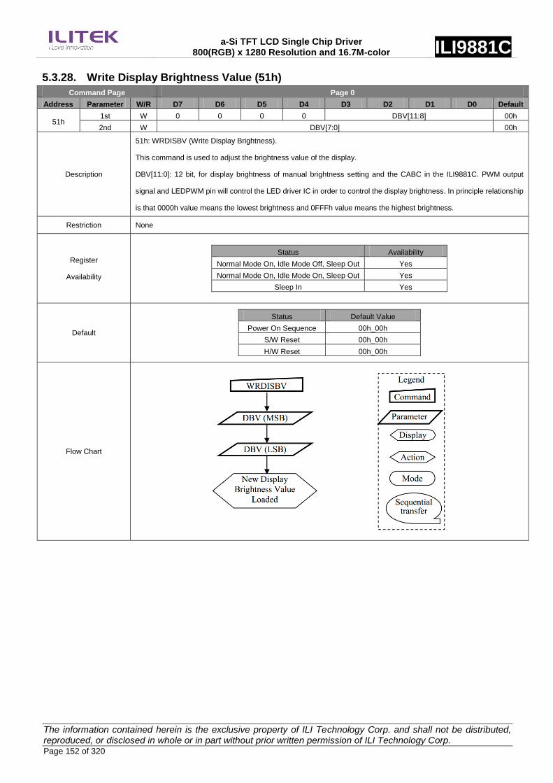
a-Si TFT LCD Single Chip Driver 800(RGB) x 1280 Resolution and 16.7M-color ILI9881C
The information contained herein is the exclusive property of ILI Technology Corp. and shall not be distributed, reproduced, or disclosed in whole or in part without prior written permission of ILI Technology Corp. Page 152 of 320
5.3.28. Write Display Brightness Value (51h)
Command Page Page 0
Address Parameter W/R D7 D6 D5 D4 D3 D2 D1 D0 Default
51h 1st W 0 0 0 0 DBV[11:8] 00h
2nd W DBV[7:0] 00h
Description
51h: WRDISBV (Write Display Brightness).
This command is used to adjust the brightness value of the display.
DBV[11:0]: 12 bit, for display brightness of manual brightness setting and the CABC in the ILI9881C. PWM output
signal and LEDPWM pin will control the LED driver IC in order to control the display brightness. In principle relationship
is that 0000h value means the lowest brightness and 0FFFh value means the highest brightness.
Restriction None
Register
Availability
Status Availability
Normal Mode On, Idle Mode Off, Sleep Out Yes
Normal Mode On, Idle Mode On, Sleep Out Yes
Sleep In Yes
Default
Status Default Value
Power On Sequence 00h_00h
S/W Reset 00h_00h
H/W Reset 00h_00h
Flow Chart
a-Si TFT LCD Single Chip Driver 800(RGB) x 1280 Resolution and 16.7M-color ILI9881C
The information contained herein is the exclusive property of ILI Technology Corp. and shall not be distributed, reproduced, or disclosed in whole or in part without prior written permission of ILI Technology Corp. Page 153 of 320
5.3.29. Read Display Brightness Value (52h)
Command Page Page 0
Address Parameter W/R D7 D6 D5 D4 D3 D2 D1 D0 Default
52h 1st R 0 0 0 0 DBV[11:8] 00h
2nd R DBV[7:0] 00h
Description
52h: RDDISBV (Read Display Brightness Value).
This command returns the brightness value of the display. It should be checked what the relationship between this
returned value and output brightness of the display. This relationship is defined on the display module specification.
In principle the relationship is that 0000h value means the lowest brightness and 0FFFh value means the highest
brightness.
DBV[11:0] is reset when display is in sleep-in mode.
DBV[11:0] is „0‟ when bit BCTRL of “5.3.30Write CTRL Display Value (53h)” command is „0‟.
DBV[11:0] is manual set brightness specified with “5.3.30Write CTRL Display Value (53h)” command when bit BCTRL
is „1‟.
Restriction None
Register
Availability
Status Availability
Normal Mode On, Idle Mode Off, Sleep Out Yes
Normal Mode On, Idle Mode On, Sleep Out Yes
Sleep In Yes
Default
Status Default Value
Power On Sequence 00h_00h
S/W Reset 00h_00h
H/W Reset 00h_00h
Flow Chart

a-Si TFT LCD Single Chip Driver 800(RGB) x 1280 Resolution and 16.7M-color ILI9881C
The information contained herein is the exclusive property of ILI Technology Corp. and shall not be distributed, reproduced, or disclosed in whole or in part without prior written permission of ILI Technology Corp. Page 154 of 320
5.3.30. Write CTRL Display Value (53h)
Command Page Page 0
Address Parameter W/R D7 D6 D5 D4 D3 D2 D1 D0 Default
53h 1st W 0 0 BCTRL 0 DD BL 0 0 00h
Description
53h: WRCTRLD (Write Control Display).
This command is used to control the display brightness.
BCTRL: Brightness Control Block On/Off. This bit is always used to switch brightness for display.
BCTRL Description
0 Brightness Control Block Off (DBV[11:0] = 0000h)
1 Brightness Control Block On (DBV[11:0] is active)
DD: Display Dimming Control.
DD Description
0 Display Dimming Off
1 Display Dimming On
BL: Backlight Control On/Off
BL Description
0 Backlight Control Off
1 Backlight Control On
Dimming function is adapted to the brightness registers for display when the bit BCTRL is changed at DD = 1, e.g.
BCTRL: 0-> 1 or 1-> 0.
When the BL bit changes from „ON‟ to „OFF‟, backlight is turned off without gradual dimming, even if Display Dimming
On (DD = 1) are selected.
Restriction None
Register
Availability
Status Availability
Normal Mode On, Idle Mode Off, Sleep Out Yes
Normal Mode On, Idle Mode On, Sleep Out Yes
Sleep In Yes
Default
Status Default Value
Power On Sequence 00h
S/W Reset 00h
H/W Reset 00h
Flow Chart

a-Si TFT LCD Single Chip Driver 800(RGB) x 1280 Resolution and 16.7M-color ILI9881C
The information contained herein is the exclusive property of ILI Technology Corp. and shall not be distributed, reproduced, or disclosed in whole or in part without prior written permission of ILI Technology Corp. Page 155 of 320
5.3.31. Read CTRL Display Value (54h)
Command Page Page 0
Address Parameter W/R D7 D6 D5 D4 D3 D2 D1 D0 Default
54h 1st R 0 0 BCTRL 0 DD BL 0 0 00h
Description
54h: RDCTRLD (Read Control Value Display).
This command returns the display brightness control values.
BCTRL: Brightness Control Block On/Off. This bit is always used to switch brightness for display.
BCTRL Description
0 Brightness Control Block Off (DBV[11:0] = 0000h)
1 Brightness Control Block On (DBV[11:0] is active)
DD: Display Dimming Control.
DD Description
0 Display Dimming Off
1 Display Dimming On
BL: Backlight Control On/Off
BL Description
0 Backlight Control Off
1 Backlight Control On
Dimming function is adapted to the brightness registers for display when the bit BCTRL is changed at DD = 1, e.g.
BCTRL: 0-> 1 or 1-> 0.
When the BL bit changes from „ON‟ to „OFF‟, backlight is turned off without gradual dimming, even if Display Dimming
On (DD = 1) are selected.
Restriction None
Register
Availability
Status Availability
Normal Mode On, Idle Mode Off, Sleep Out Yes
Normal Mode On, Idle Mode On, Sleep Out Yes
Sleep In Yes
Default
Status Default Value
Power On Sequence 00h
S/W Reset 00h
H/W Reset 00h
Flow Chart
a-Si TFT LCD Single Chip Driver 800(RGB) x 1280 Resolution and 16.7M-color ILI9881C
The information contained herein is the exclusive property of ILI Technology Corp. and shall not be distributed, reproduced, or disclosed in whole or in part without prior written permission of ILI Technology Corp. Page 156 of 320
5.3.32. Write Power Save (55h)
Command Page Page 0
Address Parameter W/R D7 D6 D5 D4 D3 D2 D1 D0 Default
55h 1st W PWRSAVE[7:0] 00h
Description
55h: PWRSAVE (Write Power Save).
This command is used to write the settings for power save control functionalities.
PWRSAVE[7:0] Function Note
00000000 Power Save Off -
00000001 Power Save Low Conservative Setting of CABC/DBLC
00000010 Power Save Medium Medium Setting of CABC/DBLC
00000011 Power Save High Aggressive Setting of CABC/DBLC
1000XXXX IE On – Low Low Enhancement of LCD
1001XXXX IE On – Medium Medium Enhancement of LCD
1011XXXX IE On – High High Enhancement of LCD
0100XXXX SRE - Low Sunlight readability enhancement
0101XXXX SRE - Medium Sunlight readability enhancement
0110XXXX SRE - High Sunlight readability enhancement
Others Reserved -
CABC = Content Adaptive Brightness Control
DBLC = Dynamic Backlight Control
IE = Image Enhancement
Restriction None
Register
Availability
Status Availability
Normal Mode On, Idle Mode Off, Sleep Out Yes
Normal Mode On, Idle Mode On, Sleep Out Yes
Sleep In Yes
Default
Status Default Value
Power On Sequence 00h
S/W Reset 00h
H/W Reset 00h
Flow Chart

a-Si TFT LCD Single Chip Driver 800(RGB) x 1280 Resolution and 16.7M-color ILI9881C
The information contained herein is the exclusive property of ILI Technology Corp. and shall not be distributed, reproduced, or disclosed in whole or in part without prior written permission of ILI Technology Corp. Page 157 of 320
5.3.33. Read Power Save (56h)
Command Page Page 0
Address Parameter W/R D7 D6 D5 D4 D3 D2 D1 D0 Default
56h 1st R PWRSAVE[7:0] 00h
Description
56h: RDPWRSAVE (Read Power Save).
This command is used to read the settings for power save control functionalities.
PWRSAVE[7:0] Function Note
00000000 Power Save Off -
00000001 Power Save Low Conservative Setting of CABC/DBLC
00000010 Power Save Medium Medium Setting of CABC/DBLC
00000011 Power Save High Aggressive Setting of CABC/DBLC
1000XXXX IE On – Low Low Enhancement of LCD
1001XXXX IE On – Medium Medium Enhancement of LCD
1011XXXX IE On – High High Enhancement of LCD
0100XXXX SRE - Low Sunlight readability enhancement
0101XXXX SRE - Medium Sunlight readability enhancement
0110XXXX SRE - High Sunlight readability enhancement
Others Reserved -
CABC = Content Adaptive Brightness Control
DBLC = Dynamic Backlight Control
IE = Image Enhancement
Restriction None
Register
Availability
Status Availability
Normal Mode On, Idle Mode Off, Sleep Out Yes
Normal Mode On, Idle Mode On, Sleep Out Yes
Sleep In Yes
Default
Status Default Value
Power On Sequence 00h
S/W Reset 00h
H/W Reset 00h
Flow Chart

a-Si TFT LCD Single Chip Driver 800(RGB) x 1280 Resolution and 16.7M-color ILI9881C
The information contained herein is the exclusive property of ILI Technology Corp. and shall not be distributed, reproduced, or disclosed in whole or in part without prior written permission of ILI Technology Corp. Page 158 of 320
5.3.34. Stop Transition (59h)
Command Page Page 0
Address Parameter W/R D7 D6 D5 D4 D3 D2 D1 D0 Default
59h - W No Argument -
Description
59h: STOP_TR (Stop Transition).
When DD bit status of “5.3.30Write CTRL Display Value (53h)” register is „1‟, applying this command instantly stops the
ongoing transition of Display Dimming.
When display module receives this command, the current output value stays active.
Restriction This command has no effect when Display Dimming transition is not active.
Register
Availability
Status Availability
Normal Mode On, Idle Mode Off, Sleep Out Yes
Normal Mode On, Idle Mode On, Sleep Out Yes
Sleep In Yes
Default
Status Default Value
Power On Sequence Off
S/W Reset Off
H/W Reset Off
Flow Chart
a-Si TFT LCD Single Chip Driver 800(RGB) x 1280 Resolution and 16.7M-color ILI9881C
The information contained herein is the exclusive property of ILI Technology Corp. and shall not be distributed, reproduced, or disclosed in whole or in part without prior written permission of ILI Technology Corp. Page 159 of 320
5.3.35. Write CABC Minimum Brightness (5Eh)
Command Page Page 0
Address Parameter W/R D7 D6 D5 D4 D3 D2 D1 D0 Default
5Eh 1st W 0 0 0 0 CMB[11:8] 00h
2nd W CMB[7:0] 00h
Description
5Eh: WRCABCMB (Write CABC minimum brightness).
This command is used to set the minimum brightness value of the display for CABC function.
In principle relationship is that 0000h value means the lowest brightness for CABC and 0FFFh value means the highest
brightness for CABC.
Restriction None
Register
Availability
Status Availability
Normal Mode On, Idle Mode Off, Sleep Out Yes
Normal Mode On, Idle Mode On, Sleep Out Yes
Sleep In Yes
Default
Status Default Value
Power On Sequence 00h_00h
S/W Reset 00h_00h
H/W Reset 00h_00h
Flow Chart

a-Si TFT LCD Single Chip Driver 800(RGB) x 1280 Resolution and 16.7M-color ILI9881C
The information contained herein is the exclusive property of ILI Technology Corp. and shall not be distributed, reproduced, or disclosed in whole or in part without prior written permission of ILI Technology Corp. Page 160 of 320
5.3.36. Read CABC Minimum Brightness (5Fh)
Command Page Page 0
Address Parameter W/R D7 D6 D5 D4 D3 D2 D1 D0 Default
5Eh 1st R 0 0 0 0 CMB[11:8] 00h
2nd R CMB[7:0] 00h
Description
5Fh: RDCABCMB (Read CABC Minimum Brightness).
This command returns the minimum brightness value of CABC function.
In principle the relationship is that 0000h value means the lowest brightness and 0FFFh value means the highest
brightness.
CMB[11:0] is CABC minimum brightness specified by the Write CABC minimum brightness (5Eh) command.
Restriction None
Register
Availability
Status Availability
Normal Mode On, Idle Mode Off, Sleep Out Yes
Normal Mode On, Idle Mode On, Sleep Out Yes
Sleep In Yes
Default
Status Default Value
Power On Sequence 00h_00h
S/W Reset 00h_00h
H/W Reset 00h_00h
Flow Chart

a-Si TFT LCD Single Chip Driver 800(RGB) x 1280 Resolution and 16.7M-color ILI9881C
The information contained herein is the exclusive property of ILI Technology Corp. and shall not be distributed, reproduced, or disclosed in whole or in part without prior written permission of ILI Technology Corp. Page 161 of 320
5.3.37. Set Transition Time (68h)
Command Page Page 0
Address Parameter W/R D7 D6 D5 D4 D3 D2 D1 D0 Default
68h 1st W TT_STP[7:0] 00h
2nd W ST_TIM[7:0] 00h
Description
68h: SET_TT (Set Transition Time).
This command controls the total transition time of Display Dimming function.
Transition time is adjusted with two parameters, defining as follows:
1st Parameter TT_STP [7:0] defines the number of dimming steps for transition.
TT_STP [7:0] Description
00h 1 step
01h 2 step
02h 4 step
03h 8 step
04h 16 step
05h 32 step
06h 64 step
07h 128 step
08h 256 step
09h 512 step
0Ah 1024 step
0Bh 2048 step
0Ch 4096 step
Others Reserved
2nd
Parameter ST_TIM [7:0] defines the step time as frame units for each dimming step.
ST_TIM [7:0] Description
00h 1 step
01h 2 step
02h 3 step
03h 4 step
04h 5 step
05h 6 step
: :
: :
FBh 252 step
FCh 253 step
FDh 254 step
FEh 255 step
FFh 256 step
Thereby, total transition time for dimming can be calculated as follows:
TT_STP [7:0] * ST_TIM [7:0] = TT, where TT unit is frame. Value 0000h means the transition is instant
Restriction None
Register
Availability
Status Availability
Normal Mode On, Idle Mode Off, Sleep Out Yes
Normal Mode On, Idle Mode On, Sleep Out Yes
Sleep In Yes

a-Si TFT LCD Single Chip Driver 800(RGB) x 1280 Resolution and 16.7M-color ILI9881C
The information contained herein is the exclusive property of ILI Technology Corp. and shall not be distributed, reproduced, or disclosed in whole or in part without prior written permission of ILI Technology Corp. Page 162 of 320
Default
Status Default Value
Power On Sequence 00h_00h
S/W Reset 00h_00h
H/W Reset 00h_00h
Flow Chart

a-Si TFT LCD Single Chip Driver 800(RGB) x 1280 Resolution and 16.7M-color ILI9881C
The information contained herein is the exclusive property of ILI Technology Corp. and shall not be distributed, reproduced, or disclosed in whole or in part without prior written permission of ILI Technology Corp. Page 163 of 320
5.3.38. Get Transition Time (69h)
Command Page Page 0
Address Parameter W/R D7 D6 D5 D4 D3 D2 D1 D0 Default
69h 1st R TT_STP[7:0] 00h
2nd R ST_TIM[7:0] 00h
Description
69h: GET_TT (Get Transition Time Value).
This readout returns the Transition Time value of Display Dimming function, described in section “5.3.37Set Transition
Time (68h)”.
Transition time is adjusted with two parameters, defining as follows:
1st Parameter TT_STP [7:0] defines the number of dimming steps for transition.
TT_STP [7:0] Description
00h 1 step
01h 2 step
02h 4 step
03h 8 step
04h 16 step
05h 32 step
06h 64 step
07h 128 step
08h 256 step
09h 512 step
0Ah 1024 step
0Bh 2048 step
0Ch 4096 step
Others Reserved
2nd
Parameter ST_TIM [7:0] defines the step time as frame units for each dimming step.
ST_TIM [7:0] Description
00h 1 step
01h 2 step
02h 3 step
03h 4 step
04h 5 step
05h 6 step
: :
: :
FBh 252 step
FCh 253 step
FDh 254 step
FEh 255 step
FFh 256 step
Restriction None
Register
Availability
Status Availability
Normal Mode On, Idle Mode Off, Sleep Out Yes
Normal Mode On, Idle Mode On, Sleep Out Yes
Sleep In Yes

a-Si TFT LCD Single Chip Driver 800(RGB) x 1280 Resolution and 16.7M-color ILI9881C
The information contained herein is the exclusive property of ILI Technology Corp. and shall not be distributed, reproduced, or disclosed in whole or in part without prior written permission of ILI Technology Corp. Page 164 of 320
Default
Status Default Value
Power On Sequence 00h_00h
S/W Reset 00h_00h
H/W Reset 00h_00h
Flow Chart

a-Si TFT LCD Single Chip Driver 800(RGB) x 1280 Resolution and 16.7M-color ILI9881C
The information contained herein is the exclusive property of ILI Technology Corp. and shall not be distributed, reproduced, or disclosed in whole or in part without prior written permission of ILI Technology Corp. Page 165 of 320
5.3.39. Read Black/White Low Bits (70h)
Command Page Page 0
Address Parameter W/R D7 D6 D5 D4 D3 D2 D1 D0 Default
70h 1st R Bkx[1:0] Bky[1:0] Wx[1:0] Wy[1:0] 00h
Description
70h: RDBWLB (Read Black/White Low Bits).
This command returns the lowest bits of black and white color characteristics.
Black: Bkx and Bky
White: Wx and Wy
Restriction None
Register
Availability
Status Availability
Normal Mode On, Idle Mode Off, Sleep Out Yes
Normal Mode On, Idle Mode On, Sleep Out Yes
Sleep In Yes
Default
Status Default Value
Power On Sequence 00h
S/W Reset 00h
H/W Reset 00h
Flow Chart

a-Si TFT LCD Single Chip Driver 800(RGB) x 1280 Resolution and 16.7M-color ILI9881C
The information contained herein is the exclusive property of ILI Technology Corp. and shall not be distributed, reproduced, or disclosed in whole or in part without prior written permission of ILI Technology Corp. Page 166 of 320
5.3.40. Read Bkx (71h)
Command Page Page 0
Address Parameter W/R D7 D6 D5 D4 D3 D2 D1 D0 Default
71h 1st R Bkx[9:2] 00h
Description 71h: RDBkx (Read Bkx).
This command reads the Bkx bits (Bkx[9:2]) of black color characteristics.
Restriction None
Register
Availability
Status Availability
Normal Mode On, Idle Mode Off, Sleep Out Yes
Normal Mode On, Idle Mode On, Sleep Out Yes
Sleep In Yes
Default
Status Default Value
Power On Sequence 00h
S/W Reset 00h
H/W Reset 00h
Flow Chart
a-Si TFT LCD Single Chip Driver 800(RGB) x 1280 Resolution and 16.7M-color ILI9881C
The information contained herein is the exclusive property of ILI Technology Corp. and shall not be distributed, reproduced, or disclosed in whole or in part without prior written permission of ILI Technology Corp. Page 167 of 320
5.3.41. Read Bky (72h)
Command Page Page 0
Address Parameter W/R D7 D6 D5 D4 D3 D2 D1 D0 Default
72h 1st R Bky[9:2] 00h
Description 72h: RDBky (Read Bky).
This command reads the Bky bits (Bky[9:2]) of black color characteristics.
Restriction None
Register
Availability
Status Availability
Normal Mode On, Idle Mode Off, Sleep Out Yes
Normal Mode On, Idle Mode On, Sleep Out Yes
Sleep In Yes
Default
Status Default Value
Power On Sequence 00h
S/W Reset 00h
H/W Reset 00h
Flow Chart

a-Si TFT LCD Single Chip Driver 800(RGB) x 1280 Resolution and 16.7M-color ILI9881C
The information contained herein is the exclusive property of ILI Technology Corp. and shall not be distributed, reproduced, or disclosed in whole or in part without prior written permission of ILI Technology Corp. Page 168 of 320
5.3.42. Read Wx (73h)
Command Page Page 0
Address Parameter W/R D7 D6 D5 D4 D3 D2 D1 D0 Default
73h 1st R Wx[9:2] 00h
Description 73h: RDWx (Read Wx).
This command reads the Wx bits (Wx[9:2]) of white color characteristics.
Restriction None
Register
Availability
Status Availability
Normal Mode On, Idle Mode Off, Sleep Out Yes
Normal Mode On, Idle Mode On, Sleep Out Yes
Sleep In Yes
Default
Status Default Value
Power On Sequence 00h
S/W Reset 00h
H/W Reset 00h
Flow Chart

a-Si TFT LCD Single Chip Driver 800(RGB) x 1280 Resolution and 16.7M-color ILI9881C
The information contained herein is the exclusive property of ILI Technology Corp. and shall not be distributed, reproduced, or disclosed in whole or in part without prior written permission of ILI Technology Corp. Page 169 of 320
5.3.43. Read Wy (74h)
Command Page Page 0
Address Parameter W/R D7 D6 D5 D4 D3 D2 D1 D0 Default
74h 1st R Wy[9:2] 00h
Description 74h: RDWy (Read Wy).
This command reads the Wy bits (Wy[9:2]) of white color characteristics.
Restriction None
Register
Availability
Status Availability
Normal Mode On, Idle Mode Off, Sleep Out Yes
Normal Mode On, Idle Mode On, Sleep Out Yes
Sleep In Yes
Default
Status Default Value
Power On Sequence 00h
S/W Reset 00h
H/W Reset 00h
Flow Chart
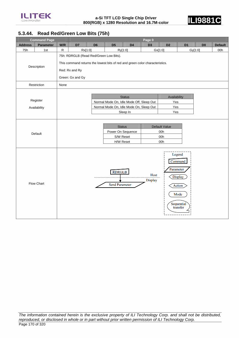
a-Si TFT LCD Single Chip Driver 800(RGB) x 1280 Resolution and 16.7M-color ILI9881C
The information contained herein is the exclusive property of ILI Technology Corp. and shall not be distributed, reproduced, or disclosed in whole or in part without prior written permission of ILI Technology Corp. Page 170 of 320
5.3.44. Read Red/Green Low Bits (75h)
Command Page Page 0
Address Parameter W/R D7 D6 D5 D4 D3 D2 D1 D0 Default
75h 1st R Rx[1:0] Ry[1:0] Gx[1:0] Gy[1:0] 00h
Description
75h: RDRGLB (Read Red/Green Low Bits).
This command returns the lowest bits of red and green color characteristics.
Red: Rx and Ry
Green: Gx and Gy
Restriction None
Register
Availability
Status Availability
Normal Mode On, Idle Mode Off, Sleep Out Yes
Normal Mode On, Idle Mode On, Sleep Out Yes
Sleep In Yes
Default
Status Default Value
Power On Sequence 00h
S/W Reset 00h
H/W Reset 00h
Flow Chart

a-Si TFT LCD Single Chip Driver 800(RGB) x 1280 Resolution and 16.7M-color ILI9881C
The information contained herein is the exclusive property of ILI Technology Corp. and shall not be distributed, reproduced, or disclosed in whole or in part without prior written permission of ILI Technology Corp. Page 171 of 320
5.3.45. Read Rx (76h)
Command Page Page 0
Address Parameter W/R D7 D6 D5 D4 D3 D2 D1 D0 Default
76h 1st R Rx[9:2] 00h
Description 76h: RDRx (Read Rx).
This command reads the Rx bits (Rx[9:2]) of red color characteristics.
Restriction None
Register
Availability
Status Availability
Normal Mode On, Idle Mode Off, Sleep Out Yes
Normal Mode On, Idle Mode On, Sleep Out Yes
Sleep In Yes
Default
Status Default Value
Power On Sequence 00h
S/W Reset 00h
H/W Reset 00h
Flow Chart

a-Si TFT LCD Single Chip Driver 800(RGB) x 1280 Resolution and 16.7M-color ILI9881C
The information contained herein is the exclusive property of ILI Technology Corp. and shall not be distributed, reproduced, or disclosed in whole or in part without prior written permission of ILI Technology Corp. Page 172 of 320
5.3.46. Read Ry (77h)
Command Page Page 0
Address Parameter W/R D7 D6 D5 D4 D3 D2 D1 D0 Default
77h 1st R Ry[9:2] 00h
Description 77h: RDRy (Read Ry).
This command reads the Ry bits (Ry[9:2]) of red color characteristics.
Restriction None
Register
Availability
Status Availability
Normal Mode On, Idle Mode Off, Sleep Out Yes
Normal Mode On, Idle Mode On, Sleep Out Yes
Sleep In Yes
Default
Status Default Value
Power On Sequence 00h
S/W Reset 00h
H/W Reset 00h
Flow Chart
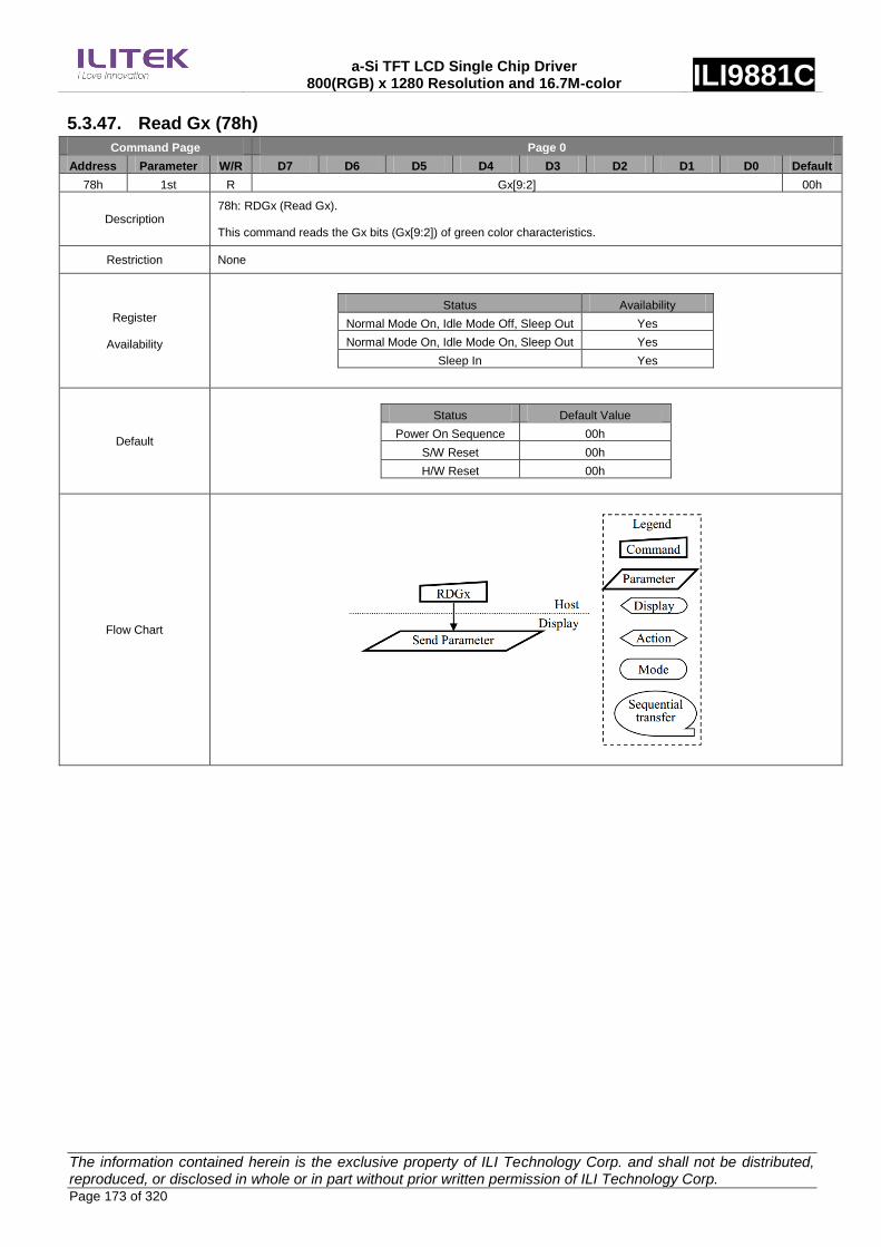
a-Si TFT LCD Single Chip Driver 800(RGB) x 1280 Resolution and 16.7M-color ILI9881C
The information contained herein is the exclusive property of ILI Technology Corp. and shall not be distributed, reproduced, or disclosed in whole or in part without prior written permission of ILI Technology Corp. Page 173 of 320
5.3.47. Read Gx (78h)
Command Page Page 0
Address Parameter W/R D7 D6 D5 D4 D3 D2 D1 D0 Default
78h 1st R Gx[9:2] 00h
Description 78h: RDGx (Read Gx).
This command reads the Gx bits (Gx[9:2]) of green color characteristics.
Restriction None
Register
Availability
Status Availability
Normal Mode On, Idle Mode Off, Sleep Out Yes
Normal Mode On, Idle Mode On, Sleep Out Yes
Sleep In Yes
Default
Status Default Value
Power On Sequence 00h
S/W Reset 00h
H/W Reset 00h
Flow Chart

a-Si TFT LCD Single Chip Driver 800(RGB) x 1280 Resolution and 16.7M-color ILI9881C
The information contained herein is the exclusive property of ILI Technology Corp. and shall not be distributed, reproduced, or disclosed in whole or in part without prior written permission of ILI Technology Corp. Page 174 of 320
5.3.48. Read Gy (79h)
Command Page Page 0
Address Parameter W/R D7 D6 D5 D4 D3 D2 D1 D0 Default
79h 1st R Gy[9:2] 00h
Description 79h: RDGy (Read Gy).
This command reads the Gy bits (Gy[9:2]) of green color characteristics.
Restriction None
Register
Availability
Status Availability
Normal Mode On, Idle Mode Off, Sleep Out Yes
Normal Mode On, Idle Mode On, Sleep Out Yes
Sleep In Yes
Default
Status Default Value
Power On Sequence 00h
S/W Reset 00h
H/W Reset 00h
Flow Chart

a-Si TFT LCD Single Chip Driver 800(RGB) x 1280 Resolution and 16.7M-color ILI9881C
The information contained herein is the exclusive property of ILI Technology Corp. and shall not be distributed, reproduced, or disclosed in whole or in part without prior written permission of ILI Technology Corp. Page 175 of 320
5.3.49. Read Blue/A Color Low Bits (7Ah)
Command Page Page 0
Address Parameter W/R D7 D6 D5 D4 D3 D2 D1 D0 Default
7Ah 1st R Bx[1:0] By[1:0] Ax[1:0] Ay[1:0] 00h
Description
7Ah: RDBALB (Read Blue/A Color Low Bits).
This command returns the lowest bits of blue and A color characteristics.
Blue: Bx and By
A: Ax and Ay
If A is not used Ax[1:0] and Ay[1:0] bits are set to „0‟s.
Restriction None
Register
Availability
Status Availability
Normal Mode On, Idle Mode Off, Sleep Out Yes
Normal Mode On, Idle Mode On, Sleep Out Yes
Sleep In Yes
Default
Status Default Value
Power On Sequence 00h
S/W Reset 00h
H/W Reset 00h
Flow Chart

a-Si TFT LCD Single Chip Driver 800(RGB) x 1280 Resolution and 16.7M-color ILI9881C
The information contained herein is the exclusive property of ILI Technology Corp. and shall not be distributed, reproduced, or disclosed in whole or in part without prior written permission of ILI Technology Corp. Page 176 of 320
5.3.50. Read Bx (7Bh)
Command Page Page 0
Address Parameter W/R D7 D6 D5 D4 D3 D2 D1 D0 Default
7Bh 1st R Bx[9:2] 00h
Description 7Bh: RDBx (Read Bx).
This command reads the Bx bits (Bx[9:2]) of blue color characteristics.
Restriction None
Register
Availability
Status Availability
Normal Mode On, Idle Mode Off, Sleep Out Yes
Normal Mode On, Idle Mode On, Sleep Out Yes
Sleep In Yes
Default
Status Default Value
Power On Sequence 00h
S/W Reset 00h
H/W Reset 00h
Flow Chart

a-Si TFT LCD Single Chip Driver 800(RGB) x 1280 Resolution and 16.7M-color ILI9881C
The information contained herein is the exclusive property of ILI Technology Corp. and shall not be distributed, reproduced, or disclosed in whole or in part without prior written permission of ILI Technology Corp. Page 177 of 320
5.3.51. Read By (7Ch)
Command Page Page 0
Address Parameter W/R D7 D6 D5 D4 D3 D2 D1 D0 Default
7Ch 1st R By[9:2] 00h
Description 7Ch: RDBy (Read By).
This command reads the By bits (By[9:2]) of blue color characteristics.
Restriction None
Register
Availability
Status Availability
Normal Mode On, Idle Mode Off, Sleep Out Yes
Normal Mode On, Idle Mode On, Sleep Out Yes
Sleep In Yes
Default
Status Default Value
Power On Sequence 00h
S/W Reset 00h
H/W Reset 00h
Flow Chart

a-Si TFT LCD Single Chip Driver 800(RGB) x 1280 Resolution and 16.7M-color ILI9881C
The information contained herein is the exclusive property of ILI Technology Corp. and shall not be distributed, reproduced, or disclosed in whole or in part without prior written permission of ILI Technology Corp. Page 178 of 320
5.3.52. Read Ax (7Dh)
Command Page Page 0
Address Parameter W/R D7 D6 D5 D4 D3 D2 D1 D0 Default
7Dh 1st R Ax[9:2] 00h
Description
7Dh: RDAx (Read Ax).
This command reads the Ax bits (Ax[9:2]) of A Color characteristics.
Ax[9:2] are set to 0 if they are not used.
Restriction None
Register
Availability
Status Availability
Normal Mode On, Idle Mode Off, Sleep Out Yes
Normal Mode On, Idle Mode On, Sleep Out Yes
Sleep In Yes
Default
Status Default Value
Power On Sequence 00h
S/W Reset 00h
H/W Reset 00h
Flow Chart

a-Si TFT LCD Single Chip Driver 800(RGB) x 1280 Resolution and 16.7M-color ILI9881C
The information contained herein is the exclusive property of ILI Technology Corp. and shall not be distributed, reproduced, or disclosed in whole or in part without prior written permission of ILI Technology Corp. Page 179 of 320
5.3.53. Read Ay (7Eh)
Command Page Page 0
Address Parameter W/R D7 D6 D5 D4 D3 D2 D1 D0 Default
7Eh 1st R Ay[9:2] 00h
Description
7Eh: RDAy (Read Ay).
This command reads the Ay bits (Ay[9:2]) of A Color characteristics.
Ay[9:2] are set to 0 if they are not used.
Restriction None
Register
Availability
Status Availability
Normal Mode On, Idle Mode Off, Sleep Out Yes
Normal Mode On, Idle Mode On, Sleep Out Yes
Sleep In Yes
Default
Status Default Value
Power On Sequence 00h
S/W Reset 00h
H/W Reset 00h
Flow Chart

a-Si TFT LCD Single Chip Driver 800(RGB) x 1280 Resolution and 16.7M-color ILI9881C
The information contained herein is the exclusive property of ILI Technology Corp. and shall not be distributed, reproduced, or disclosed in whole or in part without prior written permission of ILI Technology Corp. Page 180 of 320
5.3.54. Write Idle Mode Color (80h)
Command Page Page 0
Address Parameter W/R D7 D6 D5 D4 D3 D2 D1 D0 Default
80h 1st W 0 0 0 0 0 R G B 07h
Description
80h: WRIMCOL.
This command can be used to select color for Idle Mode.
Color selection is defined in the following table:
Default setting for color selection for “Normal Black” panel is „White‟; R=G=B:‟1‟.
Restriction None
Register
Availability
Status Availability
Normal Mode On, Idle Mode Off, Sleep Out Yes
Normal Mode On, Idle Mode On, Sleep Out Yes
Sleep In Yes
Default
Status Default Value
Power On Sequence 07h
S/W Reset 07h
H/W Reset 07h
Flow Chart

a-Si TFT LCD Single Chip Driver 800(RGB) x 1280 Resolution and 16.7M-color ILI9881C
The information contained herein is the exclusive property of ILI Technology Corp. and shall not be distributed, reproduced, or disclosed in whole or in part without prior written permission of ILI Technology Corp. Page 181 of 320
5.3.55. Read Idle Mode Color (81h)
Command Page Page 0
Address Parameter W/R D7 D6 D5 D4 D3 D2 D1 D0 Default
81h 1st R 0 0 0 0 0 R G B 07h
Description
81h: RDIMCOL.
This command returns the current color selection of Idle Mode, see section” Write Idle Mode Color (80h)”.
Color selection is defined in the following table:
Default setting for color selection for “Normal Black” panel is „White‟; R=G=B:‟1‟.
Restriction None
Register
Availability
Status Availability
Normal Mode On, Idle Mode Off, Sleep Out Yes
Normal Mode On, Idle Mode On, Sleep Out Yes
Sleep In Yes
Default
Status Default Value
Power On Sequence 07h
S/W Reset 07h
H/W Reset 07h
Flow Chart
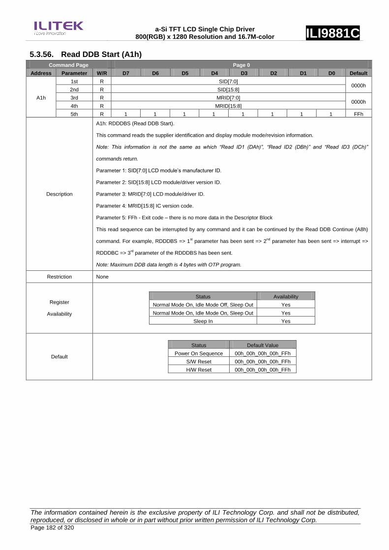
a-Si TFT LCD Single Chip Driver 800(RGB) x 1280 Resolution and 16.7M-color ILI9881C
The information contained herein is the exclusive property of ILI Technology Corp. and shall not be distributed, reproduced, or disclosed in whole or in part without prior written permission of ILI Technology Corp. Page 182 of 320
5.3.56. Read DDB Start (A1h)
Command Page Page 0
Address Parameter W/R D7 D6 D5 D4 D3 D2 D1 D0 Default
A1h
1st R SID[7:0] 0000h
2nd R SID[15:8]
3rd R MRID[7:0] 0000h
4th R MRID[15:8]
5th R 1 1 1 1 1 1 1 1 FFh
Description
A1h: RDDDBS (Read DDB Start).
This command reads the supplier identification and display module mode/revision information.
Note: This information is not the same as which “Read ID1 (DAh)”, “Read ID2 (DBh)” and “Read ID3 (DCh)”
commands return.
Parameter 1: SID[7:0] LCD module‟s manufacturer ID.
Parameter 2: SID[15:8] LCD module/driver version ID.
Parameter 3: MRID[7:0] LCD module/driver ID.
Parameter 4: MRID[15:8] IC version code.
Parameter 5: FFh - Exit code – there is no more data in the Descriptor Block
This read sequence can be interrupted by any command and it can be continued by the Read DDB Continue (A8h)
command. For example, RDDDBS => 1st parameter has been sent => 2
nd parameter has been sent => interrupt =>
RDDDBC => 3rd parameter of the RDDDBS has been sent.
Note: Maximum DDB data length is 4 bytes with OTP program.
Restriction None
Register
Availability
Status Availability
Normal Mode On, Idle Mode Off, Sleep Out Yes
Normal Mode On, Idle Mode On, Sleep Out Yes
Sleep In Yes
Default
Status Default Value
Power On Sequence 00h_00h_00h_00h_FFh
S/W Reset 00h_00h_00h_00h_FFh
H/W Reset 00h_00h_00h_00h_FFh

a-Si TFT LCD Single Chip Driver 800(RGB) x 1280 Resolution and 16.7M-color ILI9881C
The information contained herein is the exclusive property of ILI Technology Corp. and shall not be distributed, reproduced, or disclosed in whole or in part without prior written permission of ILI Technology Corp. Page 183 of 320
Flow Chart

a-Si TFT LCD Single Chip Driver 800(RGB) x 1280 Resolution and 16.7M-color ILI9881C
The information contained herein is the exclusive property of ILI Technology Corp. and shall not be distributed, reproduced, or disclosed in whole or in part without prior written permission of ILI Technology Corp. Page 184 of 320
5.3.57. Read DDB Continue (A8h)
Command Page Page 0
Address Parameter W/R D7 D6 D5 D4 D3 D2 D1 D0 Default
A8h
1st R D1[7:0] 00h
2nd R D2[7:0] 00h
: R : 00h
Nth R Dn[7:0] 00h
Description
A8h: RDDDBC (Read DDB Continue).
This command is used to read the supplier‟s identification and revision information from the point where RDDDBS
(A1h) was interrupted by another command
Restriction None
Register
Availability
Status Availability
Normal Mode On, Idle Mode Off, Sleep Out Yes
Normal Mode On, Idle Mode On, Sleep Out Yes
Sleep In Yes
Default
Status Default Value
Power On Sequence 00h
S/W Reset 00h
H/W Reset 00h
Flow Chart

a-Si TFT LCD Single Chip Driver 800(RGB) x 1280 Resolution and 16.7M-color ILI9881C
The information contained herein is the exclusive property of ILI Technology Corp. and shall not be distributed, reproduced, or disclosed in whole or in part without prior written permission of ILI Technology Corp. Page 185 of 320
5.3.58. Read First Checksum (AAh)
Command Page Page 0
Address Parameter W/R D7 D6 D5 D4 D3 D2 D1 D0 Default
AAh 1st R FCS[7:0] 00h
Description
AAh: RDFCS (Read First Checksum).
This command returns the first checksum what has been calculated from Page 0 area registers after the write access
to those registers has been done.
Restriction It will be necessary to wait 150ms after there is the last write access on Page 0 area registers before there can read
this checksum value.
Register
Availability
Status Availability
Normal Mode On, Idle Mode Off, Sleep Out Yes
Normal Mode On, Idle Mode On, Sleep Out Yes
Sleep In Yes
Default
Status Default Value
Power On Sequence 00h
S/W Reset 00h
H/W Reset 00h
Flow Chart

a-Si TFT LCD Single Chip Driver 800(RGB) x 1280 Resolution and 16.7M-color ILI9881C
The information contained herein is the exclusive property of ILI Technology Corp. and shall not be distributed, reproduced, or disclosed in whole or in part without prior written permission of ILI Technology Corp. Page 186 of 320
5.3.59. Read Continue Checksum (AFh)
Command Page Page 0
Address Parameter W/R D7 D6 D5 D4 D3 D2 D1 D0 Default
AFh 1st R CCS[7:0] 00h
Description
AFh: RDCCS (Read Continue Checksum).
This command returns the continue checksum what has been calculated continuously after the first checksum has
calculated from Page 0 area registers after the write access to those registers has been done.
Restriction It will be necessary to wait 300ms after there is the last write access on Page 0 area registers before there can read
this checksum value in the first time.
Register
Availability
Status Availability
Normal Mode On, Idle Mode Off, Sleep Out Yes
Normal Mode On, Idle Mode On, Sleep Out Yes
Sleep In Yes
Default
Status Default Value
Power On Sequence 00h
S/W Reset 00h
H/W Reset 00h
Flow Chart

a-Si TFT LCD Single Chip Driver 800(RGB) x 1280 Resolution and 16.7M-color ILI9881C
The information contained herein is the exclusive property of ILI Technology Corp. and shall not be distributed, reproduced, or disclosed in whole or in part without prior written permission of ILI Technology Corp. Page 187 of 320
5.3.60. Read ID1 (DAh)
Command Page Page 0
Address Parameter W/R D7 D6 D5 D4 D3 D2 D1 D0 Default
DAh 1st R ID1[7:0] 00h
Description
Dah: RDID1 (Read ID1).
This read byte identifies the display module‟s manufacturer.
The ID1[7:0] is programmed by the OTP function.
Restriction None
Register
Availability
Status Availability
Normal Mode On, Idle Mode Off, Sleep Out Yes
Normal Mode On, Idle Mode On, Sleep Out Yes
Sleep In Yes
Default
Status Default Value
Power On Sequence 00h
S/W Reset 00h
H/W Reset 00h
Flow Chart

a-Si TFT LCD Single Chip Driver 800(RGB) x 1280 Resolution and 16.7M-color ILI9881C
The information contained herein is the exclusive property of ILI Technology Corp. and shall not be distributed, reproduced, or disclosed in whole or in part without prior written permission of ILI Technology Corp. Page 188 of 320
5.3.61. Read ID2 (DBh)
Command Page Page 0
Address Parameter W/R D7 D6 D5 D4 D3 D2 D1 D0 Default
DBh 1st R ID2[7:0] 00h
Description
DBh: RDID2 (Read ID2).
This read byte is used to track the display module/driver version. It is defined by display supplier (with User‟s
agreement) and changes each time a revision is made to the display, material or construction specifications.
The ID2[7:0] is programmed by the OTP function.
Restriction None
Register
Availability
Status Availability
Normal Mode On, Idle Mode Off, Sleep Out Yes
Normal Mode On, Idle Mode On, Sleep Out Yes
Sleep In Yes
Default
Status Default Value
Power On Sequence 00h
S/W Reset 00h
H/W Reset 00h
Flow Chart

a-Si TFT LCD Single Chip Driver 800(RGB) x 1280 Resolution and 16.7M-color ILI9881C
The information contained herein is the exclusive property of ILI Technology Corp. and shall not be distributed, reproduced, or disclosed in whole or in part without prior written permission of ILI Technology Corp. Page 189 of 320
5.3.62. Read ID3 (DCh)
Command Page Page 0
Address Parameter W/R D7 D6 D5 D4 D3 D2 D1 D0 Default
DCh 1st R ID3[7:0] 00h
Description
DCh: RDID3 (Read ID3).
This read byte identifies the display module/driver.
The ID3[7:0] is programmed by the OTP function.
Restriction None
Register
Availability
Status Availability
Normal Mode On, Idle Mode Off, Sleep Out Yes
Normal Mode On, Idle Mode On, Sleep Out Yes
Sleep In Yes
Default
Status Default Value
Power On Sequence 00h
S/W Reset 00h
H/W Reset 00h
Flow Chart

a-Si TFT LCD Single Chip Driver 800(RGB) x 1280 Resolution and 16.7M-color ILI9881C
The information contained herein is the exclusive property of ILI Technology Corp. and shall not be distributed, reproduced, or disclosed in whole or in part without prior written permission of ILI Technology Corp. Page 190 of 320
5.3.63. EXTC Command Set Enable Register (FFh)
Command Page Page 0
Address Parameter W/R D7 D6 D5 D4 D3 D2 D1 D0 Default
FFh
1st W 1 0 0 1 1 0 0 0 98h
2nd W 1 0 0 0 0 0 0 1 81h
3rd W PAGE[7:0] 00h
Description
PAGE[7:0]: Set the command page.
PAGE[7:0] Command Page
00h Page 0
01h Page 1
02h Page 2
03h Page 3
04h Page 4
05h Page 5
06h Page 6
07h Page 7
08h Page 8
09h Page 9
0Ah Page 10
Others Reserved
Set the register, 1st Parameter = 98h, 2
nd Parameter = 81h, 3
rd Parameter = Page value to enable “Page command set”
available
See section “5.1 Command Flow”.
Restriction None
Register
Availability
Status Availability
Normal Mode On, Idle Mode Off, Sleep Out Yes
Normal Mode On, Idle Mode On, Sleep Out Yes
Sleep In Yes
Default
Status Default Value
Power On Sequence 00h
S/W Reset 00h
H/W Reset 00h
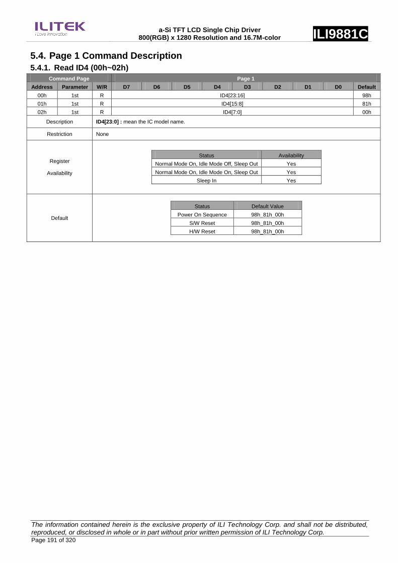
a-Si TFT LCD Single Chip Driver 800(RGB) x 1280 Resolution and 16.7M-color ILI9881C
The information contained herein is the exclusive property of ILI Technology Corp. and shall not be distributed, reproduced, or disclosed in whole or in part without prior written permission of ILI Technology Corp. Page 191 of 320
5.4. Page 1 Command Description
5.4.1. Read ID4 (00h~02h)
Command Page Page 1
Address Parameter W/R D7 D6 D5 D4 D3 D2 D1 D0 Default
00h 1st R ID4[23:16] 98h
01h 1st R ID4[15:8] 81h
02h 1st R ID4[7:0] 00h
Description ID4[23:0] : mean the IC model name.
Restriction None
Register
Availability
Status Availability
Normal Mode On, Idle Mode Off, Sleep Out Yes
Normal Mode On, Idle Mode On, Sleep Out Yes
Sleep In Yes
Default
Status Default Value
Power On Sequence 98h_81h_00h
S/W Reset 98h_81h_00h
H/W Reset 98h_81h_00h

a-Si TFT LCD Single Chip Driver 800(RGB) x 1280 Resolution and 16.7M-color ILI9881C
The information contained herein is the exclusive property of ILI Technology Corp. and shall not be distributed, reproduced, or disclosed in whole or in part without prior written permission of ILI Technology Corp. Page 192 of 320
5.4.2. Set Panel Operation Mode and Data Complement Setting (22h)
Command Page Page 1
Address Parameter W/R D7 D6 D5 D4 D3 D2 D1 D0 Default
22h 1st W/R 0 0 EPF[1:0] BGR_PA
NEL
REV_PA
NEL
SS_PAN
EL
GS_PAN
EL 30h
Description
This command defines the panel operation mode
EPF[1:0]: Set the data format from 16/18-bit (R,G,B) to 24-bit (r, g, b) that is mapping into the internal circuit.
See section “4.2.2 16/18-bit Color Data Mapping to 24-bit Pixel Data Operation” for detail description.
BGR_PANEL:
Symbol Name Description
BGR_PANEL Panel RGB-BGR Order Color selector switch control
(0=RGB color filter panel, 1=BGR color filter panel)
REV_ PANEL: Normally white or normally black panel select.
REV_PANEL Panel Data Color Source
0 Normally black 0x00 Black Smallest gamma voltage
0xFF White Largest gamma voltage
1 normally white 0x00 Black Largest gamma voltage
0xFF White Smallest gamma voltage
SS_ PANEL: Select the shift direction of outputs from the source driver.
SS_PANEL Source Output Scan Direction
0 Forward
1 Backward
GS_ PANEL: Select the shift direction of outputs from the gate driver.
GS_PANEL Gate Output Scan Direction
0 Top Bottom
1 Bottom Top
Restriction None
Register
Availability
Status Availability
Normal Mode On, Idle Mode Off, Sleep Out Yes
Normal Mode On, Idle Mode On, Sleep Out Yes
Sleep In Yes
Default
Status Default Value
(Before OTP program)
Power On Sequence 30h
S/W Reset 30h
H/W Reset 30h
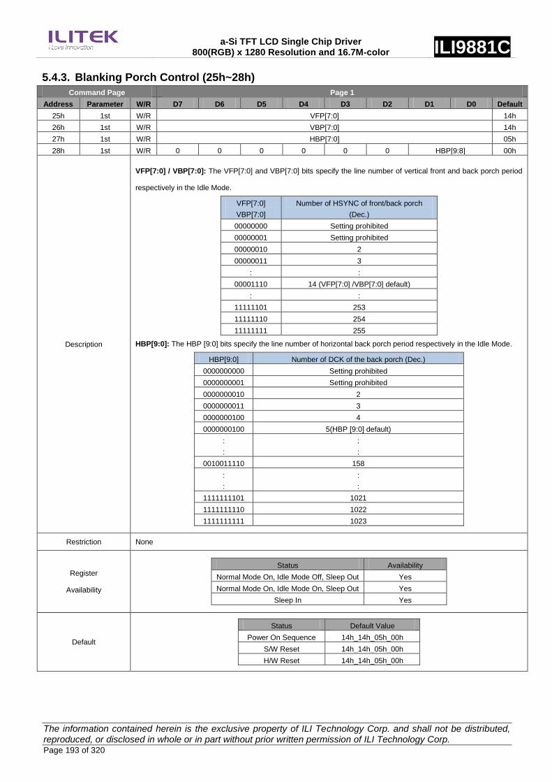
a-Si TFT LCD Single Chip Driver 800(RGB) x 1280 Resolution and 16.7M-color ILI9881C
The information contained herein is the exclusive property of ILI Technology Corp. and shall not be distributed, reproduced, or disclosed in whole or in part without prior written permission of ILI Technology Corp. Page 193 of 320
5.4.3. Blanking Porch Control (25h~28h)
Command Page Page 1
Address Parameter W/R D7 D6 D5 D4 D3 D2 D1 D0 Default
25h 1st W/R VFP[7:0] 14h
26h 1st W/R VBP[7:0] 14h
27h 1st W/R HBP[7:0] 05h
28h 1st W/R 0 0 0 0 0 0 HBP[9:8] 00h
Description
VFP[7:0] / VBP[7:0]: The VFP[7:0] and VBP[7:0] bits specify the line number of vertical front and back porch period
respectively in the Idle Mode.
VFP[7:0]
VBP[7:0]
Number of HSYNC of front/back porch
(Dec.)
00000000 Setting prohibited
00000001 Setting prohibited
00000010 2
00000011 3
: :
00001110 14 (VFP[7:0] /VBP[7:0] default)
: :
11111101 253
11111110 254
11111111 255
HBP[9:0]: The HBP [9:0] bits specify the line number of horizontal back porch period respectively in the Idle Mode.
HBP[9:0] Number of DCK of the back porch (Dec.)
0000000000 Setting prohibited
0000000001 Setting prohibited
0000000010 2
0000000011 3
0000000100 4
0000000100 5(HBP [9:0] default)
:
:
:
:
0010011110 158
:
:
:
:
1111111101 1021
1111111110 1022
1111111111 1023
Restriction None
Register
Availability
Status Availability
Normal Mode On, Idle Mode Off, Sleep Out Yes
Normal Mode On, Idle Mode On, Sleep Out Yes
Sleep In Yes
Default
Status Default Value
Power On Sequence 14h_14h_05h_00h
S/W Reset 14h_14h_05h_00h
H/W Reset 14h_14h_05h_00h
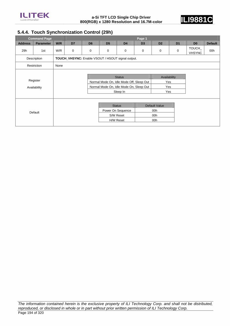
a-Si TFT LCD Single Chip Driver 800(RGB) x 1280 Resolution and 16.7M-color ILI9881C
The information contained herein is the exclusive property of ILI Technology Corp. and shall not be distributed, reproduced, or disclosed in whole or in part without prior written permission of ILI Technology Corp. Page 194 of 320
5.4.4. Touch Synchronization Control (29h)
Command Page Page 1
Address Parameter W/R D7 D6 D5 D4 D3 D2 D1 D0 Default
29h 1st W/R 0 0 0 0 0 0 0 TOUCH_
VHSYNC 00h
Description TOUCH_VHSYNC: Enable VSOUT / HSOUT signal output.
Restriction None
Register
Availability
Status Availability
Normal Mode On, Idle Mode Off, Sleep Out Yes
Normal Mode On, Idle Mode On, Sleep Out Yes
Sleep In Yes
Default
Status Default Value
Power On Sequence 00h
S/W Reset 00h
H/W Reset 00h

a-Si TFT LCD Single Chip Driver 800(RGB) x 1280 Resolution and 16.7M-color ILI9881C
The information contained herein is the exclusive property of ILI Technology Corp. and shall not be distributed, reproduced, or disclosed in whole or in part without prior written permission of ILI Technology Corp. Page 195 of 320
5.4.5. Gate Number (2Eh)
Command Page Page 1
Address Parameter W/R D7 D6 D5 D4 D3 D2 D1 D0 Default
2Eh 1st W/R NL[7:0] C8h
Description
NL[7:0]: Set the number of lines to drive the LCD at an interval of 4 lines. The number of lines must be the same or
more than the number of lines necessary for the size of the LCD panel.
NL[7:0] The Line Number of the LCD
00h 480
01h 484
02h 488
03h 492
: :
C5h 1268
C6h 1272
C7h 1276
C8h 1280
Others Reserved
Restriction None
Register
Availability
Status Availability
Normal Mode On, Idle Mode Off, Sleep Out Yes
Normal Mode On, Idle Mode On, Sleep Out Yes
Sleep In Yes
Default
Status Default Value
Power On Sequence C8h
S/W Reset C8h
H/W Reset C8h

a-Si TFT LCD Single Chip Driver 800(RGB) x 1280 Resolution and 16.7M-color ILI9881C
The information contained herein is the exclusive property of ILI Technology Corp. and shall not be distributed, reproduced, or disclosed in whole or in part without prior written permission of ILI Technology Corp. Page 196 of 320
5.4.6. Display Inversion Control (31h)
Command Page Page 1
Address Parameter W/R D7 D6 D5 D4 D3 D2 D1 D0 Default
31h 1st W/R 0 0 0 0 DINV[3:0] 00h
Description
DINV[3:0]: Set Inversion mode
NLA[3:0] Inversion
0h Column inversion
1h 1-dot inversion
2h 2-dot inversion
3h 3-dot inversion
4h 4-dot inversion
5h N/4-dot inversion Note
6h N/8-dot inversion Note
7h N/16-dot inversion Note
8h N/32-dot inversion Note
9h Zig-Zag inversion Type 1
Ah Zig-Zag inversion Type 2
Bh Zig-Zag inversion Type 3
Ch Zig-Zag inversion Type 4
Others Reserved
Note : N=The line number of the LCD (setting by NL[7:0])
Column Inversion
1st frame
2 line
1 line
3 line
4 line
2nd frame
2 line
1 line
3 line
4 line
- + - + -
+
-
+
-+
- + -
+ -
+
+
-
- -
+
+
+
-
- + - + -
+
-
+
-+
- + -
+ -
+
+
-
- -
+
+
+
-
1-Dot Inversion
1st frame
2 line
1 line
3 line
4 line
2nd frame
2 line
1 line
3 line
4 line
+ - + - + -
+ - + -
+ - + -
+ -
+
-
+
-
- -
+
+
+- + - + -
+ - + -
+ - + -
+ -
+
-
+
-
--
+
+
1st frame
2 line
1 line
3 line
4 line
2nd frame
2 line
1 line
3 line
4 line
- + - + -
+
-
+
-+
- +-
+ -
+
+
-
- -
+
+
+
-
- + - + -
+
-
+
-+
- +-
+ -
+
+
-
--
+
+
+
-
2-Dot Inversion

a-Si TFT LCD Single Chip Driver 800(RGB) x 1280 Resolution and 16.7M-color ILI9881C
The information contained herein is the exclusive property of ILI Technology Corp. and shall not be distributed, reproduced, or disclosed in whole or in part without prior written permission of ILI Technology Corp. Page 197 of 320
1st frame
2 line
1 line
3 line
4 line
2nd frame
2 line
1 line
3 line
4 line
- + - + -
+
-
+
-+
- + -
+ -
+
+
-
- -
+
+
+
-
- + - + -
+
-
+
-+
- +-
+ -
+
+
-
--
+
+
+
-
3-Dot Inversion
+ - + - +
+ +-- -
-
+6 line
5 line
6 line
5 line + - + - +
+ +- --
-
+
1st frame
2 line
1 line
3 line
4 line
2nd frame
2 line
1 line
3 line
4 line
- + - + -
+
-
+
-+
- + -
- +
+
-
-
+ +
+
-
+
-
- + - + -
+
-
+
-+
- +-
- +
+
-
-
++
+
-
+
-
4-Dot Inversion
+ - + - +
-
+
-
+-
+ - +
+ -
-
+
+
- -
-
+
-
+6 line
5 line
7 line
8 line
6 line
5 line
7 line
8 line
+ - + - +
-
+
-
+-
+ -+
+ -
-
+
+
--
-
+
-
+
Restriction None
Register
Availability
Status Availability
Normal Mode On, Idle Mode Off, Sleep Out Yes
Normal Mode On, Idle Mode On, Sleep Out Yes
Sleep In Yes
Default
Status Default Value
Power On Sequence 00h
S/W Reset 00h
H/W Reset 00h

a-Si TFT LCD Single Chip Driver 800(RGB) x 1280 Resolution and 16.7M-color ILI9881C
The information contained herein is the exclusive property of ILI Technology Corp. and shall not be distributed, reproduced, or disclosed in whole or in part without prior written permission of ILI Technology Corp. Page 198 of 320
5.4.7. Dithering Enable (34h)
Command Page Page 1
Address Parameter W/R D7 D6 D5 D4 D3 D2 D1 D0 Default
34h 1st W/R 0 0 0 0 0 0 0 DITH_EN 00h
Description
DITH_EN:
0 : dithering function disable
1 : dithering function enable
Restriction None
Register
Availability
Status Availability
Normal Mode On, Idle Mode Off, Sleep Out Yes
Normal Mode On, Idle Mode On, Sleep Out Yes
Sleep In Yes
Default
Status Default Value
Power On Sequence 00h
S/W Reset 00h
H/W Reset 00h

a-Si TFT LCD Single Chip Driver 800(RGB) x 1280 Resolution and 16.7M-color ILI9881C
The information contained herein is the exclusive property of ILI Technology Corp. and shall not be distributed, reproduced, or disclosed in whole or in part without prior written permission of ILI Technology Corp. Page 199 of 320
5.4.8. Pump Clock Adjustment (40h~43h)
Command Page Page 1
Address Parameter W/R D7 D6 D5 D4 D3 D2 D1 D0 Default
40h 1st W/R 0 EXT_CPCK_SEL[1:0] 1 0 0 VCL_CL
K_EN
VGHL_C
LK_EN 33h
41h 1st W/R 0 VCL_CLK_SELA[2:0] 0 VCL_CLK_SELB[2:0] 33h
42h 1st W/R 0 VGHL_CLK_SELA[2:0] 0 VGHL_CLK_SELB[2:0] 44h
43h 1st W/R 0 4002_RATIO_FREQA[2:0] 0 4002_RATIO_FREQB[2:0] 55h
Description
EXT_CPCK_SEL[1:0]: Pumping clock control signals selection to external control IC (ILI4003).Set the register before
Sleep Out(R11h), when external pumping control be used.
EXT_CPCK_SEL[1:0] EXTP & EXTN Output
0h Output x 1.5 waveform
1h Output x 2 waveform
2h Output x 3 waveform
3h Output Low (power down)
VCL_CLK_EN: Enable the pumping cycle of step-up circuit of VCL.
VGHL_CLK_EN: Enable the pumping cycle of step-up circuit of VGH and VGL.
VCL_CLK_SELA[2:0]: Selects the pumping cycle of step-up circuit of VCL in the Normal Mode.
VCL_CLK_SELB[2:0]: Selects the pumping cycle of step-up circuit of VCL in the Idle Mode.
VGHL_CLK_SELA[2:0]: Selects the pumping cycle of step-up circuit of VGH and VGL in the Normal Mode.
VGHL_CLK_SELB[2:0]: Selects the pumping cycle of step-up circuit of VGH and VGL in the Idle Mode.
4002_RATIO_FREQA[2:0]: Selects the pumping cycle of step-up circuit of external control IC (ILI4003) in the Normal
Mode.
4002_RATIO_FREQB[2:0]: Selects the pumping cycle of step-up circuit of external control IC (ILI4003) in the Idle
Mode.
Select the optimal step-up factor for the operating voltage. To reduce power consumption, set a smaller factor.
VGHL_CLK_SELA[2:0], VGHL_CLK_SELB[2:0]
VCL_CLK_SELA[2:0], VCL_CLK_SELB[2:0]
4002_RATIO_FREQA[2:0], 4002_RATIO_FREQB[2:0]
Pumping cycle
0h 16H
1h 8H
2h 4H
3h 2H
4h 1H
5h 1/2H
Others Reserved
Restriction None
Register
Availability
Status Availability
Normal Mode On, Idle Mode Off, Sleep Out Yes
Normal Mode On, Idle Mode On, Sleep Out Yes
Sleep In Yes

a-Si TFT LCD Single Chip Driver 800(RGB) x 1280 Resolution and 16.7M-color ILI9881C
The information contained herein is the exclusive property of ILI Technology Corp. and shall not be distributed, reproduced, or disclosed in whole or in part without prior written permission of ILI Technology Corp. Page 200 of 320
Default
Status Default Value
Power On Sequence 33h_33h_44h_55h
S/W Reset 33h_33h_44h_55h
H/W Reset 33h_33h_44h_55h

a-Si TFT LCD Single Chip Driver 800(RGB) x 1280 Resolution and 16.7M-color ILI9881C
The information contained herein is the exclusive property of ILI Technology Corp. and shall not be distributed, reproduced, or disclosed in whole or in part without prior written permission of ILI Technology Corp. Page 201 of 320
5.4.9. Power Control 1 (50h~51h)
Command Page Page 1
Address Parameter W/R D7 D6 D5 D4 D3 D2 D1 D0 Default
50h 1st W/R VREG1[7:0] 95h
51h 1st W/R VREG2[7:0] 95h
Description
VREG1[7:0]: Set the VREG1OUT voltage for positive Gamma. (12mV/step)
VREG1[7:0] VREG1OUT voltage (V)
10h 2.892
11h 2.904
12h 2.916
13h 2.928
14h 2.94
15h 2.952
: :
94h 4.476
95h 4.488
96h 4.5
: :
E8h 5.484
E9h 5.496
EAh 5.508
Other Reserved
VREG2[7:0]: Set the VREG2OUT voltage for negative Gamma. (12mV/step)
VREG2[7:0] VREG2OUT voltage (V)
10h -2.892
11h -2.904
12h -2.916
13h -2.928
14h -2.94
15h -2.952
: :
94h -4.476
95h -4.488
96h -4.5
: :
E8h -5.484
E9h -5.496
EAh -5.508
Other Reserved
Restriction None
Register
Availability
Status Availability
Normal Mode On, Idle Mode Off, Sleep Out Yes
Normal Mode On, Idle Mode On, Sleep Out Yes
Sleep In Yes
a-Si TFT LCD Single Chip Driver 800(RGB) x 1280 Resolution and 16.7M-color ILI9881C
The information contained herein is the exclusive property of ILI Technology Corp. and shall not be distributed, reproduced, or disclosed in whole or in part without prior written permission of ILI Technology Corp. Page 202 of 320
Default
Status Default Value
Power On Sequence 95h_95h
S/W Reset 95h_95h
H/W Reset 95h_95h

a-Si TFT LCD Single Chip Driver 800(RGB) x 1280 Resolution and 16.7M-color ILI9881C
The information contained herein is the exclusive property of ILI Technology Corp. and shall not be distributed, reproduced, or disclosed in whole or in part without prior written permission of ILI Technology Corp. Page 203 of 320
5.4.10. VCOM Control 1 (52h~56h)
Command Page Page 1
Address Parameter W/R D7 D6 D5 D4 D3 D2 D1 D0 Default
52h 1st W/R 0 0 0 0 0 0 0 VCM1[8] 00h
53h 1st W/R VCM1[7:0] 7Bh
54h 1st W/R 0 0 0 0 0 0 0 VCM2[8] 00h
55h 1st W/R VCM2[7:0] 7Bh
56h 1st W/R 0 0 0 NVM2 0 0 0 NVM1 00h
Description
VCM1[8:0]: Set the VCOM level when vertical forward scan (GS_PANEL= 1‟b0). (12mV/step)
VCM2[8:0]: Set the VCOM level when vertical backward scan (GS_PANEL= 1‟b1). (12mV/step)
VCM1[8:0]
VCM2[8:0] VCOM voltage (V)
010h -0.204
011h -0.216
012h -0.228
013h -0.24
014h -0.252
015h -0.264
: :
07Ah -1.476
07Bh -1.488
07Ch -1.5
: :
149h -3.96
14Ah -3.972
14Bh -3.984
14Ch -3.996
14Dh -4.008
Others Reserved
Note: VCOM ≧ VSN + 0.5V
NVM1 : Selection of the VCM setting. When the NV memory is programmed, the NVM1 will be set as „1‟ automatically.
0 : Register 52h and 53h for VCM setting
1 : NV Memory selected for VCM setting
NVM2 : Selection of the VCM setting. When the NV memory is programmed, the NVM2 will be set as „1‟ automatically.
0 : Register 54h and 55h for VCM setting
1 : NV Memory selected for VCM setting
Restriction None
Register
Availability
Status Availability
Normal Mode On, Idle Mode Off, Sleep Out Yes
Normal Mode On, Idle Mode On, Sleep Out Yes
Sleep In Yes
Default
Status Default Value
Power On Sequence 00h_7Bh_00h_7Bh_00h
S/W Reset 00h_7Bh_00h_7Bh_00h
H/W Reset 00h_7Bh_00h_7Bh_00h

a-Si TFT LCD Single Chip Driver 800(RGB) x 1280 Resolution and 16.7M-color ILI9881C
The information contained herein is the exclusive property of ILI Technology Corp. and shall not be distributed, reproduced, or disclosed in whole or in part without prior written permission of ILI Technology Corp. Page 204 of 320
5.4.11. Entry Mode Set (58h)
Command Page Page 1
Address Parameter W/R D7 D6 D5 D4 D3 D2 D1 D0 Default
58h 1st W/R LVD_EN 0 0 0 0 0 0 0 00h
Description
LVD_EN: Low voltage detection control.
LVD Low voltage detection
0 Enable
1 Disable
Restriction
Register
Availability
Status Availability
Normal Mode On, Idle Mode Off, Sleep Out Yes
Normal Mode On, Idle Mode On, Sleep Out Yes
Sleep In Yes
Default
Status Default Value
Power On Sequence 00h
S/W Reset 00h
H/W Reset 00h

a-Si TFT LCD Single Chip Driver 800(RGB) x 1280 Resolution and 16.7M-color ILI9881C
The information contained herein is the exclusive property of ILI Technology Corp. and shall not be distributed, reproduced, or disclosed in whole or in part without prior written permission of ILI Technology Corp. Page 205 of 320
5.4.12. Source Timing Adjust (60h~63h)
Command Page Page 1
Address Parameter W/R D7 D6 D5 D4 D3 D2 D1 D0 Default
60h 1st W/R 0 0 SDT[5:0] 14h
61h 1st W/R 0 0 CRT[5:0] 00h
62h 1st W/R 0 0 EQT[5:0] 19h
63h 1st W/R 0 0 PCT[5:0] 10h
Description
SDT[5:0]: Source SD timing adjustment (time scale: internal TOP_CLK). The timing can be adjusted 0 to 63 time scales.
CRT[5:0]: Source CR timing adjustment (time scale: internal TOP_CLK). The timing can be adjusted 0 to 63 time scales.
EQT[5:0]: Source EQ timing adjustment (time scale: internal TOP_CLK). The timing can be adjusted 8 to 71 time scales.
PCT[5:0]: Source PC timing adjustment (time scale: internal TOP_CLK). The timing can be adjusted 0 to 63 time scales.
Note: TOP_CLK: 62.5ns
G(N)
G(N+1)
CRT
EQT
PCT
CR(to VCI or VCL)
EQ(to GND)
PC(to VCL or VCI)
SDT
CRT
EQT
PCT
SDT
Source channel (n)
Source channel (n+1)
G(N+2)
DDVDH
DDVDL
VCI
VCL
Ground
Restriction None
Register
Availability
Status Availability
Normal Mode On, Idle Mode Off, Sleep Out Yes
Normal Mode On, Idle Mode On, Sleep Out Yes
Sleep In Yes
Default
Status Default Value
Power On Sequence 14h_00h_19h_10h
S/W Reset 14h_00h_19h_10h
H/W Reset 14h_00h_19h_10h

a-Si TFT LCD Single Chip Driver 800(RGB) x 1280 Resolution and 16.7M-color ILI9881C
The information contained herein is the exclusive property of ILI Technology Corp. and shall not be distributed, reproduced, or disclosed in whole or in part without prior written permission of ILI Technology Corp. Page 206 of 320
5.4.13. Positive Gamma Correction (A0h~B3h)
Command Page Page 1
Address Parameter W/R D7 D6 D5 D4 D3 D2 D1 D0 Default
A0h 1st W/R 0 0 VP0[5:0] 00h
A1h 1st W/R 0 VP4[6:0] 0Dh
A2h 1st W/R 0 VP8[6:0] 1Dh
A3h 1st W/R 0 0 VP12[5:0] 11h
A4h 1st W/R 0 0 VP16[5:0] 0Ch
A5h 1st W/R 0 VP24[6:0] 23h
A6h 1st W/R 0 0 VP36[5:0] 17h
A7h 1st W/R 0 0 VP52[5:0] 1Ch
A8h 1st W/R VP80[7:0] 82h
A9h 1st W/R 0 0 VP111[5:0] 21h
AAh 1st W/R 0 0 VP144[5:0] 2Ah
ABh 1st W/R VP175[7:0] 6Bh
ACh 1st W/R 0 0 VP203[5:0] 19h
ADh 1st W/R 0 0 VP219[5:0] 14h
AEh 1st W/R 0 VP231[6:0] 45h
AFh 1st W/R 0 0 VP239[5:0] 1Dh
B0h 1st W/R 0 0 VP243[5:0] 23h
B1h 1st W/R 0 VP247[6:0] 52h
B2h 1st W/R 0 VP251[6:0] 63h
B3h 1st W/R 0 0 VP255[5:0] 39h
Description Set the gray scale voltage to adjust the Gamma characteristics of the TFT panel.
Restriction None
Register
Availability
Status Availability
Normal Mode On, Idle Mode Off, Sleep Out Yes
Normal Mode On, Idle Mode On, Sleep Out Yes
Sleep In Yes
Default
Status Default Value
Power On Sequence 00h_0Dh_1Dh_11h_0Ch_23h_17h_1Ch_82h_21h
2Ah_6Bh_19h_14h_45h_1Dh_23h_52h_63h_39h
S/W Reset 00h_0Dh_1Dh_11h_0Ch_23h_17h_1Ch_82h_21h
2Ah_6Bh_19h_14h_45h_1Dh_23h_52h_63h_39h
H/W Reset 00h_0Dh_1Dh_11h_0Ch_23h_17h_1Ch_82h_21h
2Ah_6Bh_19h_14h_45h_1Dh_23h_52h_63h_39h

a-Si TFT LCD Single Chip Driver 800(RGB) x 1280 Resolution and 16.7M-color ILI9881C
The information contained herein is the exclusive property of ILI Technology Corp. and shall not be distributed, reproduced, or disclosed in whole or in part without prior written permission of ILI Technology Corp. Page 207 of 320
5.4.14. Pad Control (B6h~B7h)
Command Page Page 1
Address Parameter W/R D7 D6 D5 D4 D3 D2 D1 D0 Default
B6h 1st W/R IM_SW_
EN IM_SW[2:0]
RS_SW_
EN 0 RS_SW[1:0] 00h
B7h 1st W/R 0 0 0 0 0 0 LANSEL
_SW_EN
LANSEL
_SW 00h
Description
IM_SW_EN: Enable/Disable the lane sequence and polarity from internal command setting. The external hardware pin
IM[2:0] has no effect when IM_SW_EN is “1”.
IM_SW[2:0]: Set the configuration of lane sequence and polarity. (The bottom table is an example for MIPI 4 lane
setting)
Internal Pad Control Configuration of MIPI Lane
IM_SW2 IM_SW1 IM_SW0 D0P/N Pin D1P/N Pin CLKP/N Pin D2P/N Pin D3P/N Pin
0 0 0 D3P/N D2P/N CLKP/N D1P/N D0P/N
0 0 1 D3N/P D2N/P CLKN/P D1N/P D0N/P
0 1 0 D0P/N D1P/N CLKP/N D2P/N D3P/N
0 1 1 D0N/P D1N/P CLKN/P D2N/P D3N/P
1 0 0 D3P/N D0P/N CLKP/N D1P/N D2P/N
1 0 1 D3N/P D0N/P CLKN/P D1N/P D2N/P
1 1 0 D2P/N D1P/N CLKP/N D0P/N D3P/N
1 1 1 D2N/P D1N/P CLKN/P D0N/P D3N/P
RS_SW_EN: Enable/Disable the resolution from internal command setting. The external hardware pin RS[1:0] has no
effect when RS_SW_EN is “1”.
RS_SW[1:0]: Set the resolution.
RS_SW1 RS_SW0 Resolution
0 0 800 (RGB) x (480 + (4 x NL)) gate line
0 1 768 (RGB) x (480 + (4 x NL)) gate line
1 0 720 (RGB) x (480 + (4 x NL)) gate line
1 1 640 (RGB) x (480 + (4 x NL)) gate line
LANSEL_SW_EN: Enable/Disable the lane number from internal command setting. The external hardware pin
LANSEL has no effect when LANSEL_SW_EN is “1”.
LANSEL_SW: Set the lane number.
LANSEL_SW=”1”, MIPI DSI is 2 Lane mode LANSEL_SW=”0”, MIPI DSI is 3 or 4 Lane mode
Note: Please reference “Table 2: DSI Interface Lane Mode Selection”
Restriction
Register
Availability
Status Availability
Normal Mode On, Idle Mode Off, Sleep Out Yes
Normal Mode On, Idle Mode On, Sleep Out Yes
Sleep In Yes
Default
Status Default Value
Power On Sequence 00h_00h
S/W Reset 00h_00h
H/W Reset 00h_00h
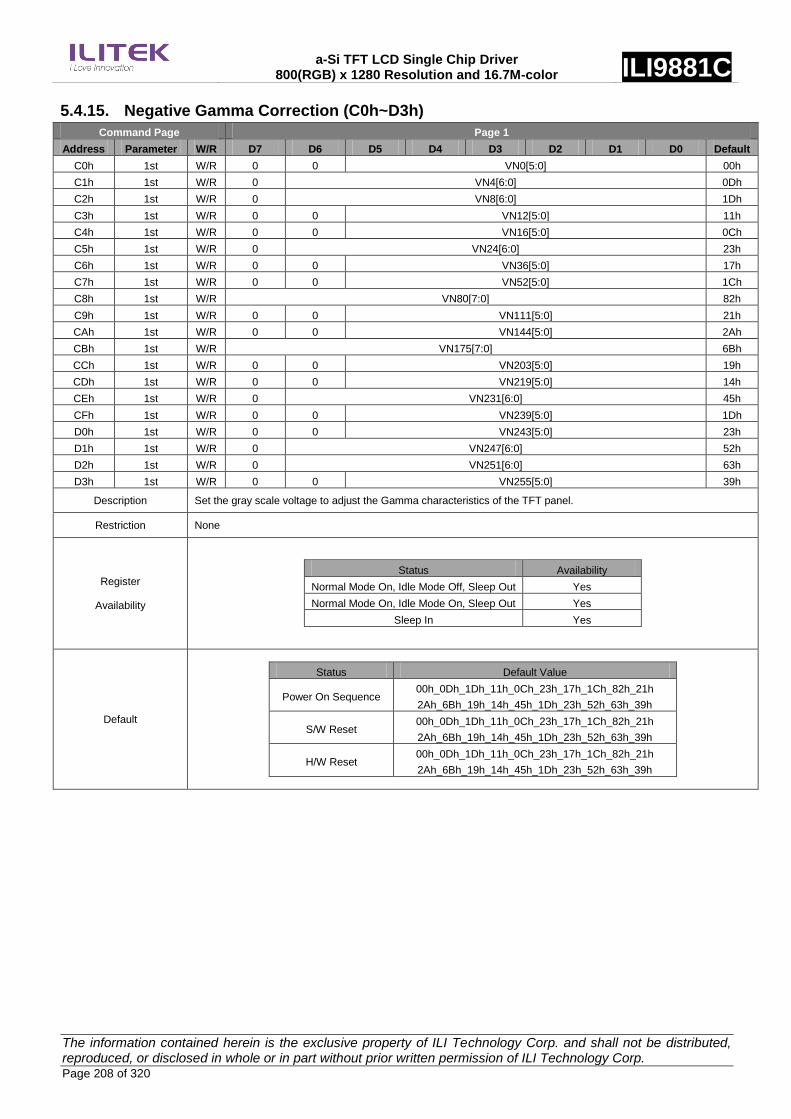
a-Si TFT LCD Single Chip Driver 800(RGB) x 1280 Resolution and 16.7M-color ILI9881C
The information contained herein is the exclusive property of ILI Technology Corp. and shall not be distributed, reproduced, or disclosed in whole or in part without prior written permission of ILI Technology Corp. Page 208 of 320
5.4.15. Negative Gamma Correction (C0h~D3h)
Command Page Page 1
Address Parameter W/R D7 D6 D5 D4 D3 D2 D1 D0 Default
C0h 1st W/R 0 0 VN0[5:0] 00h
C1h 1st W/R 0 VN4[6:0] 0Dh
C2h 1st W/R 0 VN8[6:0] 1Dh
C3h 1st W/R 0 0 VN12[5:0] 11h
C4h 1st W/R 0 0 VN16[5:0] 0Ch
C5h 1st W/R 0 VN24[6:0] 23h
C6h 1st W/R 0 0 VN36[5:0] 17h
C7h 1st W/R 0 0 VN52[5:0] 1Ch
C8h 1st W/R VN80[7:0] 82h
C9h 1st W/R 0 0 VN111[5:0] 21h
CAh 1st W/R 0 0 VN144[5:0] 2Ah
CBh 1st W/R VN175[7:0] 6Bh
CCh 1st W/R 0 0 VN203[5:0] 19h
CDh 1st W/R 0 0 VN219[5:0] 14h
CEh 1st W/R 0 VN231[6:0] 45h
CFh 1st W/R 0 0 VN239[5:0] 1Dh
D0h 1st W/R 0 0 VN243[5:0] 23h
D1h 1st W/R 0 VN247[6:0] 52h
D2h 1st W/R 0 VN251[6:0] 63h
D3h 1st W/R 0 0 VN255[5:0] 39h
Description Set the gray scale voltage to adjust the Gamma characteristics of the TFT panel.
Restriction None
Register
Availability
Status Availability
Normal Mode On, Idle Mode Off, Sleep Out Yes
Normal Mode On, Idle Mode On, Sleep Out Yes
Sleep In Yes
Default
Status Default Value
Power On Sequence 00h_0Dh_1Dh_11h_0Ch_23h_17h_1Ch_82h_21h
2Ah_6Bh_19h_14h_45h_1Dh_23h_52h_63h_39h
S/W Reset 00h_0Dh_1Dh_11h_0Ch_23h_17h_1Ch_82h_21h
2Ah_6Bh_19h_14h_45h_1Dh_23h_52h_63h_39h
H/W Reset 00h_0Dh_1Dh_11h_0Ch_23h_17h_1Ch_82h_21h
2Ah_6Bh_19h_14h_45h_1Dh_23h_52h_63h_39h

a-Si TFT LCD Single Chip Driver 800(RGB) x 1280 Resolution and 16.7M-color ILI9881C
The information contained herein is the exclusive property of ILI Technology Corp. and shall not be distributed, reproduced, or disclosed in whole or in part without prior written permission of ILI Technology Corp. Page 209 of 320
5.4.16. NV Memory Write (E0h~E2h)
Command Page Page 1
Address Parameter W/R D7 D6 D5 D4 D3 D2 D1 D0 Default
E0h 1st W/R PGM_DATA[7:0] 00h
E1h 1st W/R PGM_ADR[7:0] 00h
E2h 1st W/R PGM_ADR[15:8] 00h
Description
This command is used to program or read the NV memory data.
After a successful OTP operation, the information of PGM_DATA[7:0] will be programmed to the NV memory.
PGM_DATA[7:0]: The programmed data.
PGM_ADR[15:0]: Set the address of the NV memory for programming data. See chapter 15 “NV Memory
Programming Flow”.
PGM_ADR[15:0] Programming data
1h ID1
2h ID2
3h ID3
4h VCM1[8]
5h VCM1[7:0]
6h VCM2[8]
7h VCM2[7:0]
8h VREG1[7:0]
9h VREG2[7:0]
68h~7Bh REGAM0_P~ REGAM255_P
7Ch~8Fh REGAM0_N~ REGAM255_N
Restriction None
Register
Availability
Status Availability
Normal Mode On, Idle Mode Off, Sleep Out Yes
Normal Mode On, Idle Mode On, Sleep Out Yes
Sleep In Yes
Default
Status Default Value
Power On Sequence 00h_00h_00h
S/W Reset 00h_00h_00h
H/W Reset 00h_00h_00h

a-Si TFT LCD Single Chip Driver 800(RGB) x 1280 Resolution and 16.7M-color ILI9881C
The information contained herein is the exclusive property of ILI Technology Corp. and shall not be distributed, reproduced, or disclosed in whole or in part without prior written permission of ILI Technology Corp. Page 210 of 320
5.4.17. NV Memory Protection Key (E3h~E5h)
Command Page Page 1
Address Parameter W/R D7 D6 D5 D4 D3 D2 D1 D0 Default
E3h 1st W/R KEY[23:16] 00h
E4h 1st W/R KEY[15:8] 00h
E5h 1st W/R KEY[7:0] 00h
Description
KEY[23:0]: NV memory programming protection key.
Write an OTP data to PGM_DATA[7:0], this KEY[23:0] must set 0x55AA66h to enable OTP programming. If the
KEY[23:0] is not 0x55AA66h, the NV Memory program will be aborted.
Restriction None
Register
Availability
Status Availability
Normal Mode On, Idle Mode Off, Sleep Out Yes
Normal Mode On, Idle Mode On, Sleep Out Yes
Sleep In Yes
Default
Status Default Value
Power On Sequence 00h_00h_00h
S/W Reset 00h_00h_00h
H/W Reset 00h_00h_00h

a-Si TFT LCD Single Chip Driver 800(RGB) x 1280 Resolution and 16.7M-color ILI9881C
The information contained herein is the exclusive property of ILI Technology Corp. and shall not be distributed, reproduced, or disclosed in whole or in part without prior written permission of ILI Technology Corp. Page 211 of 320
5.4.18. NV Memory Status Read (E6h~E9h)
Command Page Page 1
Address Parameter W/R D7 D6 D5 D4 D3 D2 D1 D0 Default
E6h 1st R 0 ID2_MK[2:0] 0 ID1_MK[2:0] 00h
E7h 1st R 0 0 0 0 0 ID3_MK[2:0] 00h
E8h 1st R GAMMA
P_MK
GAMMA
N_MK VCM2_MK[2:0] VCM1_MK[2:0] 00h
E9h 1st R OTP_BU
SY 0 0 0 0 0 0 0 00h
Description
These registers uses a mark to record the NV memory programmed time. The bits are increase “+1” automatically after
writing the PGM_DATA [7:0] to the NV memory.
ID1_MK[2:0]/ID2_MK[2:0]:
ID1_MK[2:0] / ID2_MK[2:0] Description
0 0 0 No Programmed
0 0 1 Programmed 1 time already
0 1 1 Programmed 2 times already
1 1 1 Programmed 3 times already
ID3_MK[2:0]:
ID3_MK[2:0] Description
0 0 0 No Programmed
0 0 1 Programmed 1 time already
0 1 1 Programmed 2 times already
1 1 1 Programmed 3 times already
VCM1_MK[2:0] /VCM2_MK[2:0]:
VCM1_MK[2:0] / VCM2_MK[2:0] Description
0 0 0 No Programmed
0 0 1 Programmed 1 time already
0 1 1 Programmed 2 times already
1 1 1 Programmed 3 times already
GAMP_MK / GAMN_MK :
GAMP_MK / GAMN_MK Description
0 No Programmed
1 Programmed 1 time already
OTP BUSY: The status bit of the NV memory programming.
OTP_BUSY The Status of NV Memory
0 Idle
1 Busy
Restriction None
Register
Availability
Status Availability
Normal Mode On, Idle Mode Off, Sleep Out Yes
Normal Mode On, Idle Mode On, Sleep Out Yes
Sleep In Yes

a-Si TFT LCD Single Chip Driver 800(RGB) x 1280 Resolution and 16.7M-color ILI9881C
The information contained herein is the exclusive property of ILI Technology Corp. and shall not be distributed, reproduced, or disclosed in whole or in part without prior written permission of ILI Technology Corp. Page 212 of 320
Default
Status Default Value
Power On Sequence 00h_00h_00h_00h
S/W Reset 00h_00h_00h_00h
H/W Reset 00h_00h_00h_00h

a-Si TFT LCD Single Chip Driver 800(RGB) x 1280 Resolution and 16.7M-color ILI9881C
The information contained herein is the exclusive property of ILI Technology Corp. and shall not be distributed, reproduced, or disclosed in whole or in part without prior written permission of ILI Technology Corp. Page 213 of 320
5.4.19. Time Stamp (F0h~F1h)
Command Page Page 1
Address Parameter W/R D7 D6 D5 D4 D3 D2 D1 D0 Default
F0h 1st W/R Time_Stamp_Week[7:0] 00h
F1h 1st W/R Time_Stamp_Year[7:0] 00h
Description
This command identifies the display module‟s manufacture date
Time_Stamp_Week[7:0]: Week of manufacture.
Time_Stamp_Year[7:0]: Year of manufacture.
Restriction
Register
Availability
Status Availability
Normal Mode On, Idle Mode Off, Sleep Out Yes
Normal Mode On, Idle Mode On, Sleep Out Yes
Sleep In Yes
Default
Status Default Value
Power On Sequence 00h_00h
S/W Reset 00h_00h
H/W Reset 00h_00h
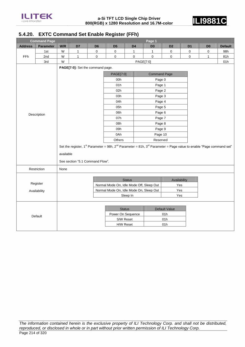
a-Si TFT LCD Single Chip Driver 800(RGB) x 1280 Resolution and 16.7M-color ILI9881C
The information contained herein is the exclusive property of ILI Technology Corp. and shall not be distributed, reproduced, or disclosed in whole or in part without prior written permission of ILI Technology Corp. Page 214 of 320
5.4.20. EXTC Command Set Enable Register (FFh)
Command Page Page 1
Address Parameter W/R D7 D6 D5 D4 D3 D2 D1 D0 Default
FFh
1st W 1 0 0 1 1 0 0 0 98h
2nd W 1 0 0 0 0 0 0 1 81h
3rd W PAGE[7:0] 01h
Description
PAGE[7:0]: Set the command page.
PAGE[7:0] Command Page
00h Page 0
01h Page 1
02h Page 2
03h Page 3
04h Page 4
05h Page 5
06h Page 6
07h Page 7
08h Page 8
09h Page 9
0Ah Page 10
Others Reserved
Set the register, 1st Parameter = 98h, 2
nd Parameter = 81h, 3
rd Parameter = Page value to enable “Page command set”
available
See section “5.1 Command Flow”.
Restriction None
Register
Availability
Status Availability
Normal Mode On, Idle Mode Off, Sleep Out Yes
Normal Mode On, Idle Mode On, Sleep Out Yes
Sleep In Yes
Default
Status Default Value
Power On Sequence 01h
S/W Reset 01h
H/W Reset 01h
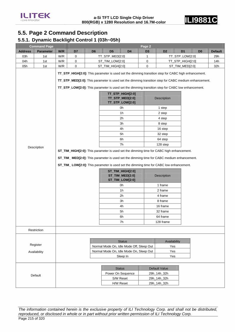
a-Si TFT LCD Single Chip Driver 800(RGB) x 1280 Resolution and 16.7M-color ILI9881C
The information contained herein is the exclusive property of ILI Technology Corp. and shall not be distributed, reproduced, or disclosed in whole or in part without prior written permission of ILI Technology Corp. Page 215 of 320
5.5. Page 2 Command Description
5.5.1. Dynamic Backlight Control 1 (03h~05h)
Command Page Page 2
Address Parameter W/R D7 D6 D5 D4 D3 D2 D1 D0 Default
03h 1st W/R 0 TT_STP_MED[2:0] 1 TT_STP_LOW[2:0] 29h
04h 1st W/R 0 ST_TIM_LOW[2:0] 0 TT_STP_HIGH[2:0] 14h
05h 1st W/R 0 ST_TIM_HIGH[2:0] 0 ST_TIM_MED[2:0] 32h
Description
TT_STP_HIGH[2:0]: This parameter is used set the dimming transition step for CABC high enhancement.
TT_STP_MED[2:0]: This parameter is used set the dimming transition step for CABC medium enhancement.
TT_STP_LOW[2:0]: This parameter is used set the dimming transition step for CABC low enhancement.
TT_STP_HIGH[2:0]
TT_STP_MED[2:0]
TT_STP_LOW[2:0]
Description
0h 1 step
1h 2 step
2h 4 step
3h 8 step
4h 16 step
5h 32 step
6h 64 step
7h 128 step
ST_TIM_HIGH[2:0]: This parameter is used set the dimming time for CABC high enhancement.
ST_TIM_ MED[2:0]: This parameter is used set the dimming time for CABC medium enhancement.
ST_TIM_ LOW[2:0]: This parameter is used set the dimming time for CABC low enhancement.
ST_TIM_HIGH[2:0]
ST_TIM_MED[2:0]
ST_TIM_LOW[2:0]
Description
0h 1 frame
1h 2 frame
2h 4 frame
3h 8 frame
4h 16 frame
5h 32 frame
6h 64 frame
7h 128 frame
Restriction
Register
Availability
Status Availability
Normal Mode On, Idle Mode Off, Sleep Out Yes
Normal Mode On, Idle Mode On, Sleep Out Yes
Sleep In Yes
Default
Status Default Value
Power On Sequence 29h_14h_32h
S/W Reset 29h_14h_32h
H/W Reset 29h_14h_32h

a-Si TFT LCD Single Chip Driver 800(RGB) x 1280 Resolution and 16.7M-color ILI9881C
The information contained herein is the exclusive property of ILI Technology Corp. and shall not be distributed, reproduced, or disclosed in whole or in part without prior written permission of ILI Technology Corp. Page 216 of 320
5.5.2. Dynamic Backlight Control 2 (06h~07h)
Command Page Page 2
Address Parameter W/R D7 D6 D5 D4 D3 D2 D1 D0 Default
06h 1st W/R 0 PWM_DUTY_PRECISION[2:0] 0 LEDPW
M_POL
LEDON_
POL LEDON 00h
07h 1st W/R PWM_DIV[7:0] 0Eh
Description
LEDON: The bit is used to define LEDON enable.
LEDON_POL: The bit is used to define polarity of LEDON.
LEDPWM_POL: The bit is used to define polarity of LEDPWM signal.
BL LEDPWM_POL LEDPWM pin
0 0 Always low
0 1 Always high
1 0 Original polarity of LEDPWM signal
1 1 Inversed polarity of LEDPWM signal
PWM_DUTY_PRECISION[2:0] / PWM_DIV[7:0]: LEDPWM output period control. This command is used to adjust the
PWM waveform period of PWM_OUT. The PWM period is calculated using the following equation.
PWM_DUTY_PRECISION[2:0] PWM_DUTY_PRECISION fLEDPWM (MAX)
(PWM_DIV[7:0]=0)
fLEDPWM (min)
(PWM_DIV[7:0]=255)
0h 4096 7.8 KHz 31 Hz
1h 2048 15.6 KHz 61 Hz
2h 1024 31.2 KHz 122 Hz
3h 512 62.5 KHz 244 Hz
4h 256 125 KHz 488 Hz
5h~7h Reserved X X
tperiod
tontoff
LEDPWM
CABC ON
Note : The output frequency tolerance of internal frequency divider in CABC is ±10%
X = void.
Restriction
Register
Availability
Status Availability
Normal Mode On, Idle Mode Off, Sleep Out Yes
Normal Mode On, Idle Mode On, Sleep Out Yes
Sleep In Yes
Default
Status Default Value
Power On Sequence 00h_0Eh
S/W Reset 00h_0Eh
H/W Reset 00h_0Eh

a-Si TFT LCD Single Chip Driver 800(RGB) x 1280 Resolution and 16.7M-color ILI9881C
The information contained herein is the exclusive property of ILI Technology Corp. and shall not be distributed, reproduced, or disclosed in whole or in part without prior written permission of ILI Technology Corp. Page 217 of 320
5.5.3. IIE Function Control (10h~19h)
Command Page Page 2
Address Parameter W/R D7 D6 D5 D4 D3 D2 D1 D0 Default
10h 1st W/R 0 0 0 AXIS_EN 0 PRT_EN SKIN_EN 0 06h
11h 1st W/R 0 AUTO_M
EAN 0 0 CN_EN CN_INV SHP_EN 0 00h
12h 1st W/R 0 0 0 0 0 0 CN_LV[1:0] 02h
13h 1st W/R 0 0 SHP_LV[1:0] SRE_MIDIV_LV[1:0] 0 0 20h
15h 1st W/R RGB_MEAN[7:0] 80h
16h 1st W/R
SRE_HY
STERESI
S_EN
0 0 SRE_DI
M_EN
SRE_SC
_EN
SRE_CE
_EN 0 0 1Ch
17h 1st W/R 0 SRE_OFFS[2:0] 0 SRE_DIM_STP[2:0] 01h
18h 1st W/R SRE_DIM_FRAME[7:0] 08h
19h 1st W/R SRE_SC_GAIN_ADJ[2:0] SRE_HYSTERESIS_LIMIT[4:0] C0h
Description
AXIS_EN: Enable the 24-axis adjustment of saturation enhancement.
PRT_EN: Enable the over-saturation protection of saturation enhancement.
SKIN_EN: Enable the skin-tone protection of saturation enhancement.
AUTO_MEAN: Enable auto image mean calculation RGB_MEAN[7:0] is not available when AUTO_MEAN=1h.
CN_EN: Enable contrast enhancement.
CN_INV: Select contrast enhancement Function.
CN_INV Contrast Function
0 Contrast increase
1 Contrast decrease
SHP_EN: Enable sharpness enhancement.
CN_LV[1:0] : Define contrast enhancement level.
SRE_MIDIV_LV[1:0] : Define SRE medium level enhancement select.
SRE_MIDIV_LV[1:0] Enhancement level
00h / 11h Level_M
01h Level_H
10h Level_L
SHP_LV[1:0] : Define sharpness enhancement level.
CN_LV[1:0]
SHP_LV[1:0] Enhancement level
0h Level_L
1h Level_M
2h Level_H
RGB_MEAN[7:0]: Setting image mean value, available when AUTO_MEAN=0h.
SRE_HYSTERESIS_EN: SRE hysteresis mode enable signal.
SRE_DIM_EN: SRE dimming function enable signal.
SRE_SC_EN: SRE saturation compensation enable.
SRE_CE_EN: SRE contrast enhancement enable.
SRE_OFFS[2:0]: SRE offset value
SRE_DIM_STP[2:0]: Setting the number of dimming steps for transition
SRE_DIM_STP[2:0] Description
0h 2 step
1h 4 step
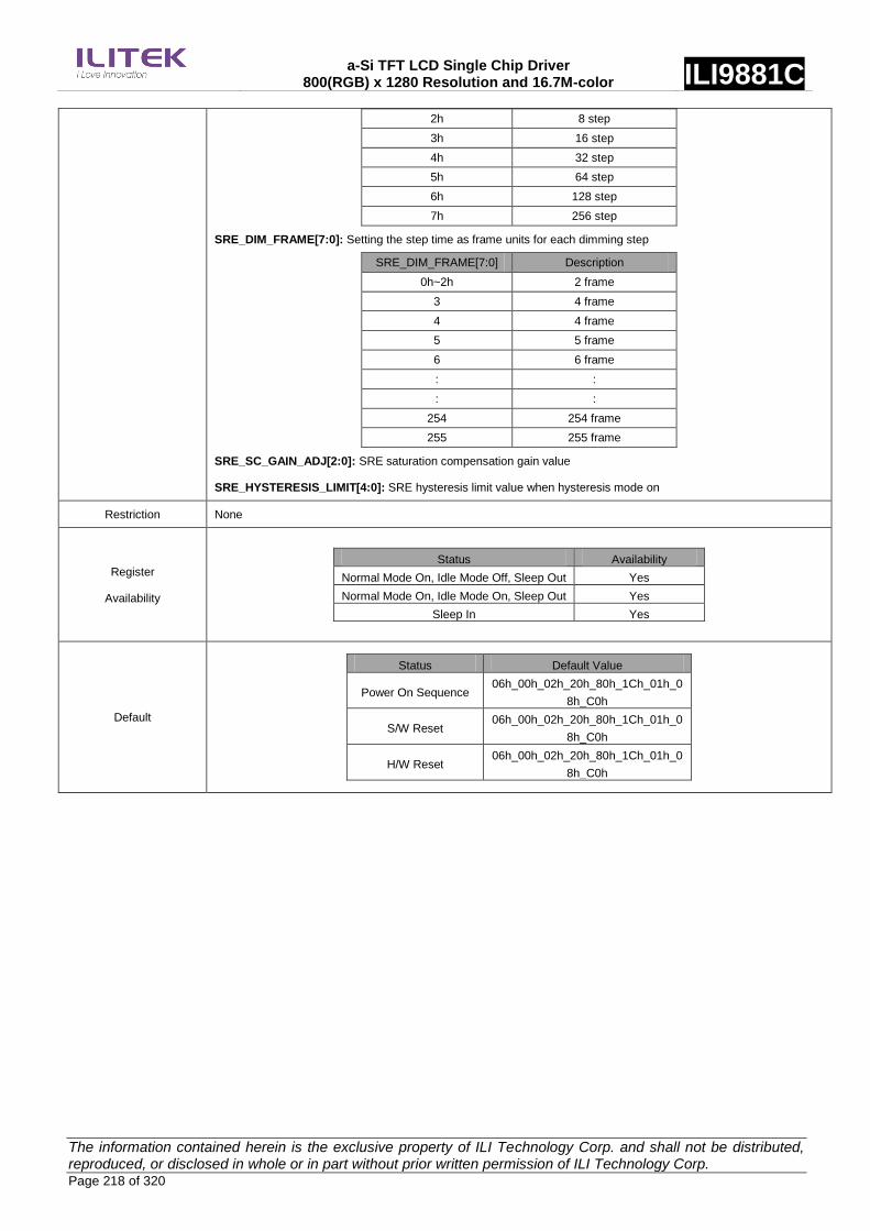
a-Si TFT LCD Single Chip Driver 800(RGB) x 1280 Resolution and 16.7M-color ILI9881C
The information contained herein is the exclusive property of ILI Technology Corp. and shall not be distributed, reproduced, or disclosed in whole or in part without prior written permission of ILI Technology Corp. Page 218 of 320
2h 8 step
3h 16 step
4h 32 step
5h 64 step
6h 128 step
7h 256 step
SRE_DIM_FRAME[7:0]: Setting the step time as frame units for each dimming step
SRE_DIM_FRAME[7:0] Description
0h~2h 2 frame
3 4 frame
4 4 frame
5 5 frame
6 6 frame
: :
: :
254 254 frame
255 255 frame
SRE_SC_GAIN_ADJ[2:0]: SRE saturation compensation gain value
SRE_HYSTERESIS_LIMIT[4:0]: SRE hysteresis limit value when hysteresis mode on
Restriction None
Register
Availability
Status Availability
Normal Mode On, Idle Mode Off, Sleep Out Yes
Normal Mode On, Idle Mode On, Sleep Out Yes
Sleep In Yes
Default
Status Default Value
Power On Sequence 06h_00h_02h_20h_80h_1Ch_01h_0
8h_C0h
S/W Reset 06h_00h_02h_20h_80h_1Ch_01h_0
8h_C0h
H/W Reset 06h_00h_02h_20h_80h_1Ch_01h_0
8h_C0h

a-Si TFT LCD Single Chip Driver 800(RGB) x 1280 Resolution and 16.7M-color ILI9881C
The information contained herein is the exclusive property of ILI Technology Corp. and shall not be distributed, reproduced, or disclosed in whole or in part without prior written permission of ILI Technology Corp. Page 219 of 320
5.5.4. IIE Saturation Enhancement Control 1 (1Ah~1Ch)
Command Page Page 2
Address Parameter W/R D7 D6 D5 D4 D3 D2 D1 D0 Default
1Ah 1st W/R 0 0 SE_RATIO_L[5:0] 07h
1Bh 1st W/R 0 0 SE_RATIO_M[5:0] 09h
1Ch 1st W/R 0 0 SE_RATIO_H[5:0] 0Ch
Description
SE_RATIO_L[5:0]: Define low saturation enhancement level of User Command 55h (Page0_R55h).
SE_RATIO_M[5:0]: Define medium saturation enhancement level of User Command 55h (Page0_R55h).
SE_RATIO_H[5:0]: Define high saturation enhancement level of User Command 55h (Page0_R55h).
Saturationenhanced = Saturationoriginal + (Saturationoriginal × SE_RATIO)
SE_RATIO_L[5:0]
SE_RATIO_M[5:0]
SE_RATIO_H[5:0]
Ratio (Dec)
SE_RATIO_L[5:0]
SE_RATIO_M[5:0]
SE_RATIO_H[5:0]
Ratio (Dec)
00h 0.0 10h 1.0
01h 0.0625 11h 1.0625
02h 0.125 12h 1.125
03h 0.1875 13h 1.1875
04h 0.25 14h 1.25
05h 0.3125 15h 1.3125
06h 0.375 16h 1.375
07h 0.4375 17h 1.4375
08h 0.5 18h 1.5
09h 0.5625 19h 1.5625
0Ah 0.625 1Ah 1.625
0Bh 0.6875 1Bh 1.6875
0Ch 0.75 1Ch 1.75
0Dh 0.8125 1Dh 1.8125
0Eh 0.875 1Eh 1.875
0Fh 0.9375 1Fh 1.9375
Restriction None
Register
Availability
Status Availability
Normal Mode On, Idle Mode Off, Sleep Out Yes
Normal Mode On, Idle Mode On, Sleep Out Yes
Sleep In Yes
Default
Status Default Value
Power On Sequence 07h_09h_0Ch
S/W Reset 07h_09h_0Ch
H/W Reset 07h_09h_0Ch
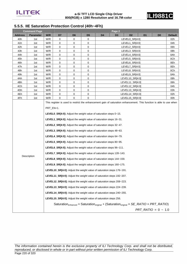
a-Si TFT LCD Single Chip Driver 800(RGB) x 1280 Resolution and 16.7M-color ILI9881C
The information contained herein is the exclusive property of ILI Technology Corp. and shall not be distributed, reproduced, or disclosed in whole or in part without prior written permission of ILI Technology Corp. Page 220 of 320
5.5.5. IIE Saturation Protection Control (40h~4Fh)
Command Page Page 2
Address Parameter W/R D7 D6 D5 D4 D3 D2 D1 D0 Default
40h 1st W/R 0 0 0 LEVEL0_SR[4:0] 02h
41h 1st W/R 0 0 0 LEVEL1_SR[4:0] 04h
42h 1st W/R 0 0 0 LEVEL2_SR[4:0] 06h
43h 1st W/R 0 0 0 LEVEL3_SR[4:0] 08h
44h 1st W/R 0 0 0 LEVEL4_SR[4:0] 0Ah
45h 1st W/R 0 0 0 LEVEL5_SR[4:0] 0Ch
46h 1st W/R 0 0 0 LEVEL6_SR[4:0] 0Eh
47h 1st W/R 0 0 0 LEVEL7_SR[4:0] 0Eh
48h 1st W/R 0 0 0 LEVEL8_SR[4:0] 0Ch
49h 1st W/R 0 0 0 LEVEL9_SR[4:0] 0Ah
4Ah 1st W/R 0 0 0 LEVEL10_SR[4:0] 08h
4Bh 1st W/R 0 0 0 LEVEL11_SR[4:0] 06h
4Ch 1st W/R 0 0 0 LEVEL12_SR[4:0] 04h
4Dh 1st W/R 0 0 0 LEVEL13_SR[4:0] 03h
4Eh 1st W/R 0 0 0 LEVEL14_SR[4:0] 02h
4Fh 1st W/R 0 0 0 LEVEL15_SR[4:0] 00h
Description
This register is used to restrict the enhancement gain of saturation enhancement. This function is able to use when
PRT_EN=1.
LEVEL0_SR[4:0]: Adjust the weight value of saturation steps 0~15.
LEVEL1_SR[4:0]: Adjust the weight value of saturation steps 16~31.
LEVEL2_SR[4:0]: Adjust the weight value of saturation steps 32~47.
LEVEL3_SR[4:0]: Adjust the weight value of saturation steps 48~63.
LEVEL4_SR[4:0]: Adjust the weight value of saturation steps 64~79.
LEVEL5_SR[4:0]: Adjust the weight value of saturation steps 80~95.
LEVEL6_SR[4:0]: Adjust the weight value of saturation steps 96~111.
LEVEL7_SR[4:0]: Adjust the weight value of saturation steps 128~143.
LEVEL8_SR[4:0]: Adjust the weight value of saturation steps 144~159.
LEVEL9_SR[4:0]: Adjust the weight value of saturation steps 160~175.
LEVEL10_SR[4:0]: Adjust the weight value of saturation steps 176~191.
LEVEL11_SR[4:0]: Adjust the weight value of saturation steps 192~207.
LEVEL12_SR[4:0]: Adjust the weight value of saturation steps 208~223.
LEVEL13_SR[4:0]: Adjust the weight value of saturation steps 224~239.
LEVEL14_SR[4:0]: Adjust the weight value of saturation steps 240~255.
LEVEL15_SR[4:0]: Adjust the weight value of saturation steps 256.
Saturationenhanced = Saturationoriginal + (Saturationoriginal × SE_RATIO × PRT_RATIO)
PRT_RATIO = 0 ~ 1.0

a-Si TFT LCD Single Chip Driver 800(RGB) x 1280 Resolution and 16.7M-color ILI9881C
The information contained herein is the exclusive property of ILI Technology Corp. and shall not be distributed, reproduced, or disclosed in whole or in part without prior written permission of ILI Technology Corp. Page 221 of 320
Restriction None
Register
Availability
Status Availability
Normal Mode On, Idle Mode Off, Sleep Out Yes
Normal Mode On, Idle Mode On, Sleep Out Yes
Sleep In Yes
Default
Status Default Value
Power On Sequence 02h_04h_06h_08h_0Ah_0Ch_0Eh_0Eh_0Ch_0Ah_08h_06h_04h_03h_02h_00h
S/W Reset 02h_04h_06h_08h_0Ah_0Ch_0Eh_0Eh_0Ch_0Ah_08h_06h_04h_03h_02h_00h
H/W Reset 02h_04h_06h_08h_0Ah_0Ch_0Eh_0Eh_0Ch_0Ah_08h_06h_04h_03h_02h_00h

a-Si TFT LCD Single Chip Driver 800(RGB) x 1280 Resolution and 16.7M-color ILI9881C
The information contained herein is the exclusive property of ILI Technology Corp. and shall not be distributed, reproduced, or disclosed in whole or in part without prior written permission of ILI Technology Corp. Page 222 of 320
5.5.6. IIE Sharpness Enhancement Control (5Ah~5Ch)
Command Page Page 2
Address Parameter W/R D7 D6 D5 D4 D3 D2 D1 D0 Default
5Ah 1st W/R 0 0 0 SHP_RATIO[4:0] 18h
5Bh 1st W/R SHP_THR_H[7:0] 64h
5Ch 1st W/R SHP_THR_L[7:0] 1Eh
Description
This register sets the enhancement level of the sharpness enhancement. This function is able to use when SHP_EN=1
SHP_RATIO[4:0]: Adjust the ratio of sharpness enhancement.
Yenh = Yorg + ( Yorg – blur(Yorg) ) × SHP_RATIO
SHP_RATIO[4:0] Ratio (Dec) SHP_RATIO[4:0] Ratio (Dec)
00h 0.0 10h 2.0
01h 0.125 11h 2.125
02h 0.25 12h 2.25
03h 0.375 13h 2.375
04h 0.5 14h 2.5
05h 0.625 15h 2.625
06h 0.75 16h 2.75
07h 0.875 17h 2.875
08h 1.0 18h 3.0
09h 1.125 19h 3.125
0Ah 1.25 1Ah 3.25
0Bh 1.375 1Bh 3.375
0Ch 1.5 1Ch 3.5
0Dh 1.625 1Dh 3.625
0Eh 1.75 1Eh 3.75
0Fh 1.875 1Fh 3.875
SHP_THR_H[7:0]: Define Sharpness enhancement upper bound threshold.
SHP_THR_L[7:0]: Define Sharpness enhancement lower bound threshold.
Restriction None
Register
Availability
Status Availability
Normal Mode On, Idle Mode Off, Sleep Out Yes
Normal Mode On, Idle Mode On, Sleep Out Yes
Sleep In Yes
Default
Status Default Value
Power On Sequence 18h_64h_1Eh
S/W Reset 18h_64h_1Eh
H/W Reset 18h_64h_1Eh

a-Si TFT LCD Single Chip Driver 800(RGB) x 1280 Resolution and 16.7M-color ILI9881C
The information contained herein is the exclusive property of ILI Technology Corp. and shall not be distributed, reproduced, or disclosed in whole or in part without prior written permission of ILI Technology Corp. Page 223 of 320
5.5.7. IIE Contrast Enhancement Control (60h~66h)
Command Page Page 2
Address Parameter W/R D7 D6 D5 D4 D3 D2 D1 D0 Default
60h 1st W/R 0 0 CN_00[5:0] 0Eh
61h 1st W/R 0 0 CN_01[5:0] 18h
62h 1st W/R 0 0 CN_02[5:0] 24h
63h 1st W/R 0 0 CN_03[5:0] 28h
64h 1st W/R 0 0 CN_04[5:0] 24h
65h 1st W/R 0 0 CN_05[5:0] 18h
66h 1st W/R 0 0 CN_06[5:0] 0Eh
Description
This register sets the weight value of the turning point of contrast gain cure. This function is able to use when CN_EN=1
CN_00[5:0]: Adjust the weight of S curve ratio of turning point 1.
CN_01[5:0]: Adjust the weight of S curve ratio of turning point 2.
CN_02[5:0]: Adjust the weight of S curve ratio of turning point 3.
CN_03[5:0]: Adjust the weight of S curve ratio of turning point 4.
CN_04[5:0]: Adjust the weight of S curve ratio of turning point 5.
CN_05[5:0]: Adjust the weight of S curve ratio of turning point 6.
CN_06[5:0]: Adjust the weight of S curve ratio of turning point 7.
Yenh = Yorg + Ydelta
cn_00
cn_03
0
T6 T5 T4 T3 T2 T1
T6T5T4T3T2T1
Ydelta
Yorg
cn_01
cn_02
T7
cn_04
cn_05
cn_06
T7 255
–Ydelta
cn_06 cn_00
cn_05 cn_01
cn_04 cn_02cn_03
Restriction None
Register
Availability
Status Availability
Normal Mode On, Idle Mode Off, Sleep Out Yes
Normal Mode On, Idle Mode On, Sleep Out Yes
Sleep In Yes
Default
Status Default Value
Power On Sequence 0Eh_18h_24h_28h_24h_18h_0Eh
S/W Reset 0Eh_18h_24h_28h_24h_18h_0Eh
H/W Reset 0Eh_18h_24h_28h_24h_18h_0Eh

a-Si TFT LCD Single Chip Driver 800(RGB) x 1280 Resolution and 16.7M-color ILI9881C
The information contained herein is the exclusive property of ILI Technology Corp. and shall not be distributed, reproduced, or disclosed in whole or in part without prior written permission of ILI Technology Corp. Page 224 of 320
5.5.8. EXTC Command Set Enable Register (FFh)
Command Page Page 2
Address Parameter W/R D7 D6 D5 D4 D3 D2 D1 D0 Default
FFh
1st W 1 0 0 1 1 0 0 0 98h
2nd W 1 0 0 0 0 0 0 1 81h
3rd W PAGE[7:0] 02h
Description
PAGE[7:0]: Set the command page.
PAGE[7:0] Command Page
00h Page 0
01h Page 1
02h Page 2
03h Page 3
04h Page 4
05h Page 5
06h Page 6
07h Page 7
08h Page 8
09h Page 9
0Ah Page 10
Others Reserved
Set the register, 1st Parameter = 98h, 2
nd Parameter = 81h, 3
rd Parameter = Page value to enable “Page command set”
available
See section “5.1 Command Flow”.
Restriction None
Register
Availability
Status Availability
Normal Mode On, Idle Mode Off, Sleep Out Yes
Normal Mode On, Idle Mode On, Sleep Out Yes
Sleep In Yes
Default
Status Default Value
Power On Sequence 02h
S/W Reset 02h
H/W Reset 02h

a-Si TFT LCD Single Chip Driver 800(RGB) x 1280 Resolution and 16.7M-color ILI9881C
The information contained herein is the exclusive property of ILI Technology Corp. and shall not be distributed, reproduced, or disclosed in whole or in part without prior written permission of ILI Technology Corp. Page 225 of 320
5.6. Page 3 Command Description
5.6.1. EXTC Command Set Enable Register (FFh)
Command Page Page 3
Address Parameter W/R D7 D6 D5 D4 D3 D2 D1 D0 Default
FFh
1st W 1 0 0 1 1 0 0 0 98h
2nd W 1 0 0 0 0 0 0 1 81h
3rd W PAGE[7:0] 03h
Description
PAGE[7:0]: Set the command page.
PAGE[7:0] Command Page
00h Page 0
01h Page 1
02h Page 2
03h Page 3
04h Page 4
05h Page 5
06h Page 6
07h Page 7
08h Page 8
09h Page 9
0Ah Page 10
Others Reserved
Set the register, 1st Parameter = 98h, 2
nd Parameter = 81h, 3
rd Parameter = Page value to enable “Page command set”
available
See section “5.1 Command Flow”.
Restriction None
Register
Availability
Status Availability
Normal Mode On, Idle Mode Off, Sleep Out Yes
Normal Mode On, Idle Mode On, Sleep Out Yes
Sleep In Yes
Default
Status Default Value
Power On Sequence 03h
S/W Reset 03h
H/W Reset 03h

a-Si TFT LCD Single Chip Driver 800(RGB) x 1280 Resolution and 16.7M-color ILI9881C
The information contained herein is the exclusive property of ILI Technology Corp. and shall not be distributed, reproduced, or disclosed in whole or in part without prior written permission of ILI Technology Corp. Page 226 of 320
5.7. Page 4 Command Description
5.7.1. DSI Lanes Control (00h)
Command Page Page 4
Address Parameter W/R D7 D6 D5 D4 D3 D2 D1 D0 Default
00h 1st W/R MIPI_LA
NE_SEL 0 0 0 0 0 0 0 80h
Description MIPI_LANE_SEL: MIPI DSI lane number selection
Note: When use this setting, please reference to chapter 4.1 “DSI System Interface”.
Restriction None
Register
Availability
Status Availability
Normal Mode On, Idle Mode Off, Sleep Out Yes
Normal Mode On, Idle Mode On, Sleep Out Yes
Sleep In Yes
Default
Status Default Value
Power On Sequence 80h
S/W Reset 80h
H/W Reset 80h

a-Si TFT LCD Single Chip Driver 800(RGB) x 1280 Resolution and 16.7M-color ILI9881C
The information contained herein is the exclusive property of ILI Technology Corp. and shall not be distributed, reproduced, or disclosed in whole or in part without prior written permission of ILI Technology Corp. Page 227 of 320
5.7.2. Touch Synchronization Timing Adjust (27h~2Ah)
Command Page Page 4
Address Parameter W/R D7 D6 D5 D4 D3 D2 D1 D0 Default
27h 1st W/R TOUCH_OPT[1:0] VSOD[1:0] HSOM[1:0] HFP_HB
P_OPT
VS_PW_
OPT 00h
28h 1st W/R HSOD[7:0] 05h
29h 1st W/R HSOHW[7:0] 19h
2Ah 1st W/R VS_OUT
_EN
HS_OUT
_EN
VS_OUT
_POL
HS_OUT
_POL 0 0 STB_EN 0 F0h
Description
This command controls the synchronization output. This function is able to use when Page1_R29h=01h.
TOUCH_OPT[1:0]: Select the Output Mode of synchronization (time scale: internal TOP_CLK)
TOUCH_OPT[1:0] Description
0h Off
1h VFP+VBP
2h Adjustable for VSOUT / HSOUT(Note 2)
3h VFP+VBP / HFP+HBP
VSOD[1:0]: Set the VSOUT delay timing (time scale: internal TOP_CLK)
VSOD[1:0] Description
0h 0 line (First line of back porch)
1h 1 line
2h 2 line
3h 3 line
HSOM[1:0]: Set the HSOUT active period (time scale: internal TOP_CLK)
HSOM[1:0] Description
0h VACT Period + VFP + VBP
1h VACT Period
2h VFP+VBP
3h Reserved
HFP_HBP_OPT: Select the output source for HSOUT
HFP_HBP_OPT Description
0 Prebuf-Source
1 HSOUT(Note 2)
VS_PW_OPT: Set the pulse width of VSOUT
VS_PW_OPT Description
0 pulse width = 1H
1
During transition from display off to display on : pulse width = 3H
During transition from display on to display off : pulse width = 2H
Otherwise : pulse width = 1H
HSOD[7:0]: Set HSOUT delay timing (time scale: internal TOP_CLK)
HSOD[1:0] Description
0h 0clk
1h 1clk
2h 2clk
: :
FDh 253clk
FEh 254clk
FFh 255clk

a-Si TFT LCD Single Chip Driver 800(RGB) x 1280 Resolution and 16.7M-color ILI9881C
The information contained herein is the exclusive property of ILI Technology Corp. and shall not be distributed, reproduced, or disclosed in whole or in part without prior written permission of ILI Technology Corp. Page 228 of 320
HSOHW[7:0]: Set the high width of HSOUT (time scale: internal TOP_CLK)
HSOHW[1:0] Description
0h Reserved
1h 1clk
2h 2clk
: :
FDh 253clk
FEh 254clk
FFh 255clk
VS_OUT_EN: VS signal output enable (1: enable, 0: disable)
HS_OUT_EN: HS signal output enable (1: enable, 0: disable)
VS_OUT_POL: VS signal polarity (1: non-inversion, 0: inversion)
HS_OUT_POL: HS signal polarity (1: non-inversion, 0: inversion)
STB_EN: touch option
Note 1: TOP_CLK: 32ns
Note 2: When use this setting, please reference to chapter 17 “Touch Synchronization Signal”.
Restriction None
Register
Availability
Status Availability
Normal Mode On, Idle Mode Off, Sleep Out Yes
Normal Mode On, Idle Mode On, Sleep Out Yes
Sleep In Yes
Default
Status Default Value
Power On Sequence 00h_05h_19h_F0h
S/W Reset 00h_05h_19h_F0h
H/W Reset 00h_05h_19h_F0h

a-Si TFT LCD Single Chip Driver 800(RGB) x 1280 Resolution and 16.7M-color ILI9881C
The information contained herein is the exclusive property of ILI Technology Corp. and shall not be distributed, reproduced, or disclosed in whole or in part without prior written permission of ILI Technology Corp. Page 229 of 320
5.7.3. BIST Mode Function (2Dh,2Fh)
Command Page Page 4
Address Parameter W/R D7 D6 D5 D4 D3 D2 D1 D0 Default
2Dh 1st W/R FRM_PT[7:0] FFh
2Fh 1st W/R 0 0 FRM_CYC[1:0] 0 0 0 FRM_E
N 00h
Description
FRM_PT[15:0]: Enable/disable the pattern
FRM_PT[15:0] Pattern
FRM_PT[0] White
FRM_PT[1] Black
FRM_PT[2] Red
FRM_PT[3] Green
FRM_PT[4] Blue
FRM_PT[5] Gray128
FRM_PT[6] Gray127
FRM_PT[7] V-Color bar
See also sections:”8 BIST Mode Function ”
FRM_CYC[1:0]: Set scan cycle of each pattern
FRM_CYC[1:0] Description
0h 64 frames
1h 128 frames
2h 256 frames
3h 512 frames
FRM_EN: Enable/disable BIST mode function
FRM_EN Description
0 Normal display
1 Enable BIST mode
Restriction None
Register
Availability
Status Availability
Normal Mode On, Idle Mode Off, Sleep Out Yes
Normal Mode On, Idle Mode On, Sleep Out Yes
Sleep In Yes
Default
Status Default Value
Power On Sequence FFh_FFh_00h
S/W Reset FFh_FFh_00h
H/W Reset FFh_FFh_00h

a-Si TFT LCD Single Chip Driver 800(RGB) x 1280 Resolution and 16.7M-color ILI9881C
The information contained herein is the exclusive property of ILI Technology Corp. and shall not be distributed, reproduced, or disclosed in whole or in part without prior written permission of ILI Technology Corp. Page 230 of 320
5.7.4. Power Control 1 (69h)
Command Page Page 4
Address Parameter W/R D7 D6 D5 D4 D3 D2 D1 D0 Default
69h 1st W/R 1 CP_VCL_CLP_OPTION_PRE[2:0] 0 1 1 1 D7h
Description
CP_VCL_CLP_OPTION_PRE[2:0]: Set VCL clamp level.
CP_VCL_CLP_OPTION_PRE[2:0] VCL clamp level (V)
0h -3.0V
1h -2.9V
2h -2.8V
3h -2.7V
4h -2.6V
5h -2.5V
6h -2.4V
7h -2.3V
Restriction None
Register
Availability
Status Availability
Normal Mode On, Idle Mode Off, Sleep Out Yes
Normal Mode On, Idle Mode On, Sleep Out Yes
Sleep In Yes
Default
Status Default Value
Power On Sequence D7h
S/W Reset D7h
H/W Reset D7h

a-Si TFT LCD Single Chip Driver 800(RGB) x 1280 Resolution and 16.7M-color ILI9881C
The information contained herein is the exclusive property of ILI Technology Corp. and shall not be distributed, reproduced, or disclosed in whole or in part without prior written permission of ILI Technology Corp. Page 231 of 320
5.7.5. VCORE Setting (6Ch)
Command Page Page 4
Address Parameter W/R D7 D6 D5 D4 D3 D2 D1 D0 Default
6Ch 1st W/R 0 0 0 1 DI_VCORE_SEL[3:0] 15h
Description
DI_VCORE_SEL[3:0]: Set VCORE voltage adjustment.
DI_VCORE_SEL[3:0] VCORE voltage (V)
0h 1.25
1h 1.30
2h 1.35
3h 1.40
4h 1.45
5h 1.50
6h 1.55
7h 1.60
8h 1.65
9h 1.70
Others Reserved
Restriction None
Register
Availability
Status Availability
Normal Mode On, Idle Mode Off, Sleep Out Yes
Normal Mode On, Idle Mode On, Sleep Out Yes
Sleep In Yes
Default
Status Default Value
Power On Sequence 15h
S/W Reset 15h
H/W Reset 15h

a-Si TFT LCD Single Chip Driver 800(RGB) x 1280 Resolution and 16.7M-color ILI9881C
The information contained herein is the exclusive property of ILI Technology Corp. and shall not be distributed, reproduced, or disclosed in whole or in part without prior written permission of ILI Technology Corp. Page 232 of 320
5.7.6. Power Control 2 (6Eh)
Command Page Page 4
Address Parameter W/R D7 D6 D5 D4 D3 D2 D1 D0 Default
6Eh 1st W/R 0 DI_PWR
_REG REG1_VRH_CP[5:0] 6Ah
Description
DI_PWR_REG: Select the input power mode.
DI_PWR_REG BOOSTM2 BOOSTM1 BOOSTM0 Note
0 0 0 1 Power Mode 2A External IOVCC, VSP and VSN (VCI=VSP)
Note 1
1 0 0 1 Power Mode 4 External IOVCC, VCI, VSP and VSN
X 0 1 0 Power Mode 3 External IOVCC and VCI (ILI4003)
prohibited -
Note 1: VCI and VSP pads must be connected by external metal path.
REG1_VRH_CP[5:0]: Set VGH clamp level. (18mV/step)
REG1_VRH_CP[5:0] VGH clamp level (V)
03h 7.98
04h 8.16
05h 8.34
06h 8.52
07h 8.7
08h 8.88
: :
29h 14.82
2Ah 15
2Bh 15.18
: :
39h 17.7
3Ah 17.88
3Bh 18.06
Other Reserved
Restriction None
Register
Availability
Status Availability
Normal Mode On, Idle Mode Off, Sleep Out Yes
Normal Mode On, Idle Mode On, Sleep Out Yes
Sleep In Yes
Default
Status Default Value
Power On Sequence 6Ah
S/W Reset 6Ah
H/W Reset 6Ah

a-Si TFT LCD Single Chip Driver 800(RGB) x 1280 Resolution and 16.7M-color ILI9881C
The information contained herein is the exclusive property of ILI Technology Corp. and shall not be distributed, reproduced, or disclosed in whole or in part without prior written permission of ILI Technology Corp. Page 233 of 320
5.7.7. Power Control 3 (6Fh)
Command Page Page 4
Address Parameter W/R D7 D6 D5 D4 D3 D2 D1 D0 Default
6Fh 1st W/R VGLREG
_EN_GO DI_CP_VGH_BH[2:0] DI_CP_VGL_BL[2:0]
DI_CP_V
CL_REG
_SEL
34h
Description
VGLREG_EN_GO: Enable/Disable VGL regulator circuit (VGLO1).
VGLREG_EN_GO VGL regulator
0 Disable
1 Enable
DI_CP_VGH_BH[2:0]: Set the factor used in the step-up circuits for VGH.
Select the optimal step-up factor for the operating voltage. To reduce power consumption, set a smaller factor.
DI_CP_VGH_BH[2:0] VGH Output
(power mode 3, 4)
VGH Output
(power mode 2) Flying Capacitor
0h Reserved Reserved -
1h 2*VSP 2*VSP C21P/N + C22P/N (option)
2h 2.5*VSP 3*VSP C21P/N + C22P/N (option)
3h 3*VSP 3*VSP C21P/N + C22P/N (option)
4h 3.5*VSP 4*VSP C21P/N + C22P/N
5h 4*VSP 4*VSP C21P/N + C22P/N
6h 4.5*VSP 5*VSP C21P/N + C22P/N
7h 5*VSP 5*VSP C21P/N + C22P/N
DI_CP_VGL_BL[2:0]: Set the factor used in the step-up circuits for VGL. Select the optimal step-up factor for the
operating voltage. To reduce power consumption, set a smaller factor.
DI_CP_VGL_BL[2:0] VGL Output
(power mode 3, 4)
VGL Output
(power mode 2) Flying Capacitor
0h -1.5*VSP -2*VSP C23P/N + C24P/N (option)
1h -2*VSP -2*VSP C23P/N + C24P/N (option)
2h -2.5*VSP -3*VSP C23P/N + C24P/N (option)
3h -3*VSP -3*VSP C23P/N + C24P/N (option)
4h -3.5*VSP -4*VSP C23P/N + C24P/N
5h -4*VSP -4*VSP C23P/N + C24P/N
6h -4.5*VSP -5*VSP C23P/N + C24P/N
7h -5*VSP -5*VSP C23P/N + C24P/N
DI_CP_VCL_REG_SEL: Set VCL power source.
DI_CP_VCL_REG_SEL VCL power source
0 Charge-pumping circuit
(Connect the C41P/C41N and C42P/C42N capacitor)
1 Regulator circuit
(Disconnect the C41P/C41N and C42P/C42N capacitor)
Restriction None
Register
Availability
Status Availability
Normal Mode On, Idle Mode Off, Sleep Out Yes
Normal Mode On, Idle Mode On, Sleep Out Yes
Sleep In Yes

a-Si TFT LCD Single Chip Driver 800(RGB) x 1280 Resolution and 16.7M-color ILI9881C
The information contained herein is the exclusive property of ILI Technology Corp. and shall not be distributed, reproduced, or disclosed in whole or in part without prior written permission of ILI Technology Corp. Page 234 of 320
Default
Status Default Value
Power On Sequence 34h
S/W Reset 34h
H/W Reset 34h
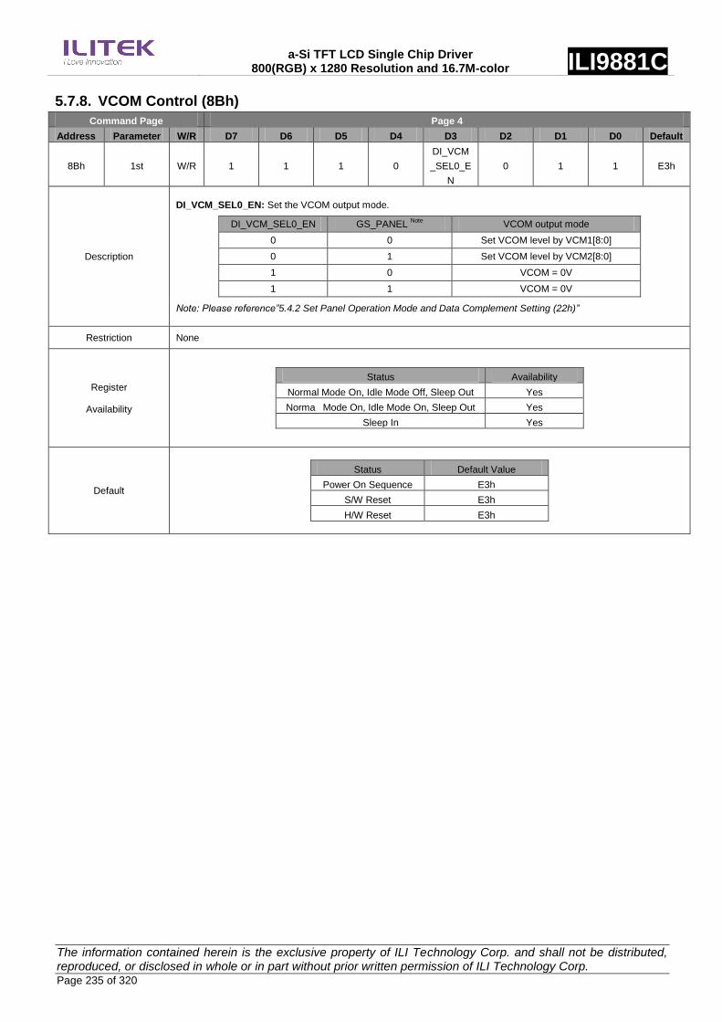
a-Si TFT LCD Single Chip Driver 800(RGB) x 1280 Resolution and 16.7M-color ILI9881C
The information contained herein is the exclusive property of ILI Technology Corp. and shall not be distributed, reproduced, or disclosed in whole or in part without prior written permission of ILI Technology Corp. Page 235 of 320
5.7.8. VCOM Control (8Bh)
Command Page Page 4
Address Parameter W/R D7 D6 D5 D4 D3 D2 D1 D0 Default
8Bh 1st W/R 1 1 1 0
DI_VCM
_SEL0_E
N
0 1 1 E3h
Description
DI_VCM_SEL0_EN: Set the VCOM output mode.
DI_VCM_SEL0_EN GS_PANEL Note
VCOM output mode
0 0 Set VCOM level by VCM1[8:0]
0 1 Set VCOM level by VCM2[8:0]
1 0 VCOM = 0V
1 1 VCOM = 0V
Note: Please reference”5.4.2 Set Panel Operation Mode and Data Complement Setting (22h)”
Restriction None
Register
Availability
Status Availability
Normal Mode On, Idle Mode Off, Sleep Out Yes
Norma Mode On, Idle Mode On, Sleep Out Yes
Sleep In Yes
Default
Status Default Value
Power On Sequence E3h
S/W Reset E3h
H/W Reset E3h

a-Si TFT LCD Single Chip Driver 800(RGB) x 1280 Resolution and 16.7M-color ILI9881C
The information contained herein is the exclusive property of ILI Technology Corp. and shall not be distributed, reproduced, or disclosed in whole or in part without prior written permission of ILI Technology Corp. Page 236 of 320
5.7.9. Power Control 4 (8Ch~8Dh)
Command Page Page 4
Address Parameter W/R D7 D6 D5 D4 D3 D2 D1 D0 Default
8Ch 1st W/R 0 DI_VCOM_REG_VGLREG[6:0] 03h
8Dh 1st W/R 0 DI_VCOM_CP_VGLCLP[6:0] 14h
Description
DI_VCOM_REG_VGLREG[6:0]: Set VGLO1 voltage adjustment. (0.18V/step)
DI_VCOM_REG_VGLREG[6:0] VGLO1 voltage (V)
03h -6.99
04h -7.17
05h -7.35
06h -7.53
07h -7.71
08h -7.89
09h -8.07
0Ah -8.25
0Bh -8.43
0Ch -8.61
0Dh -8.79
0Eh -8.97
0Fh -9.15
10h -9.33
11h -9.51
12h -9.69
13h -9.87
14h -10.05
15h -10.23
: :
3Fh -17.79
40h -17.97
41h -18.15
Others Reserved
DI_VCOM_CP_VGLCLP[6:0]: Set VGL clamp level. (18mV/step)
DI_VCOM_CP_VGLCLP[6:0] VGL clamp level (V)
03h -6.99
04h -7.17
05h -7.35
06h -7.53
07h -7.71
08h -7.89
09h -8.07
0Ah -8.25
0Bh -8.43
0Ch -8.61
0Dh -8.79
0Eh -8.97
0Fh -9.15
10h -9.33
11h -9.51
12h -9.69
13h -9.87
14h -10.05
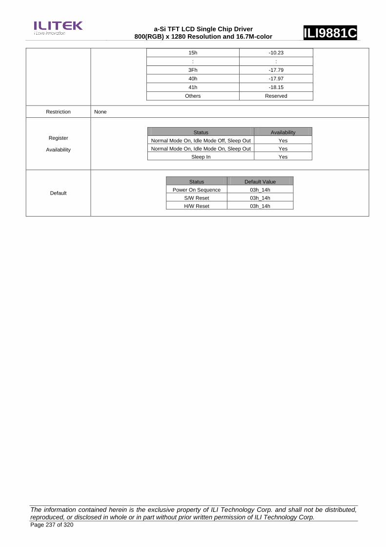
a-Si TFT LCD Single Chip Driver 800(RGB) x 1280 Resolution and 16.7M-color ILI9881C
The information contained herein is the exclusive property of ILI Technology Corp. and shall not be distributed, reproduced, or disclosed in whole or in part without prior written permission of ILI Technology Corp. Page 237 of 320
15h -10.23
: :
3Fh -17.79
40h -17.97
41h -18.15
Others Reserved
Restriction None
Register
Availability
Status Availability
Normal Mode On, Idle Mode Off, Sleep Out Yes
Normal Mode On, Idle Mode On, Sleep Out Yes
Sleep In Yes
Default
Status Default Value
Power On Sequence 03h_14h
S/W Reset 03h_14h
H/W Reset 03h_14h

a-Si TFT LCD Single Chip Driver 800(RGB) x 1280 Resolution and 16.7M-color ILI9881C
The information contained herein is the exclusive property of ILI Technology Corp. and shall not be distributed, reproduced, or disclosed in whole or in part without prior written permission of ILI Technology Corp. Page 238 of 320
5.7.10. Temperature Detecting Setting (BBh~CEh)
Command Page Page 4
Address Parameter W/R D7 D6 D5 D4 D3 D2 D1 D0 Default
BBh 1st W/R
EN_TEM
P_PROC
ESS
0 CP_VGH_TAP_C[5:0] 1Eh
BCh 1st W/R 0 0 CP_VGH_TAP_L[5:0] 1Eh
BDh 1st W/R 0 0 CP_VGH_TAP_M[5:0] 1Eh
BEh 1st W/R 0 0 CP_VGH_TAP_H[5:0] 1Eh
BFh 1st W/R VCOM_C[7:0] 4Ch
C0h 1st W/R VCOM_L[7:0] 4Ch
C1h 1st W/R VCOM_M[7:0] 4Ch
C2h 1st W/R VCOM_H[7:0] 4Ch
C8h 1st W/R TS_TH0[7:0] 00h
C9h 1st W/R TS_TH1[7:0] 00h
CAh 1st W/R TS_TH2[7:0] 00h
CBh 1st W/R TS_TH3[7:0] 00h
CCh 1st W/R TS_TH0[9:8] TS_TH1[9:8] TS_TH2[9:8] TS_TH3[9:8] 00h
CDh 1st W/R TS_DEBT_OPT[3:0] TS_HYST_OPT[3:0] 02h
CEh 1st W/R EN_TS VCOM_
C[8]
VCOM_L
[8]
VCOM_
M[8]
VCOM_
H[8] 1 0 0 04h
Description
EN_TEMP_PROCESS / EN_TS: Enable/Disable Temperature Detecting function.
EN_TEMP_PROCESS
EN_TS Function
0 0 Disable
1 1 Enable
Other Reserved
CP_VGH_TAP_C[5:0]: Set VGH clamp level for Temp_Cold. (18mV/step)
CP_VGH_TAP_L[5:0]: Set VGH clamp level for Temp_Low. (18mV/step)
CP_VGH_TAP_M[5:0]: Set VGH clamp level for Temp_Middle. (18mV/step)
CP_VGH_TAP_H[5:0]: Set VGH clamp level for Temp_High. (18mV/step)
CP_VGH_TAP_C[5:0]
CP_VGH_TAP_L[5:0]
CP_VGH_TAP_M[5:0]
CP_VGH_TAP_H[5:0]
VGH clamp level (V)
03h 7.98
04h 8.16
05h 8.34
06h 8.52
07h 8.7
08h 8.88
: :
28h 14.64
29h 14.82
2Ah 15
2Bh 15.18
2Ch 15.36
: :
37h 17.34
38h 17.52
39h 17.7

a-Si TFT LCD Single Chip Driver 800(RGB) x 1280 Resolution and 16.7M-color ILI9881C
The information contained herein is the exclusive property of ILI Technology Corp. and shall not be distributed, reproduced, or disclosed in whole or in part without prior written permission of ILI Technology Corp. Page 239 of 320
3Ah 17.88
3Bh 18.06
Other Reserved
VCOM_C[8:0]: Set the VCOM level for Temp_Cold.
VCOM_L[8:0]: Set the VCOM level for Temp_Low.
VCOM_M[8:0]: Set the VCOM level for Temp_Middle.
VCOM_H[8:0]: Set the VCOM level for Temp_High.
VCOM_C[8:0]
VCOM_L[8:0]
VCOM_M[8:0]
VCOM_H[8:0]
VCOM voltage (V)
010h -0.204
011h -0.216
012h -0.228
013h -0.24
014h -0.252
015h -0.264
: :
07Ah -1.476
07Bh -1.488
07Ch -1.5
: :
149h -3.96
14Ah -3.972
14Bh -3.984
14Ch -3.996
14Dh -4.008
Others Reserved
TS_TH0[9:0]: Set the temperature detecting range threshold for Temp_Cold.
TS_TH1[9:0]: Set the temperature detecting range threshold for Temp_Low.
TS_TH2[9:0]: Set the temperature detecting range threshold for Temp_Middle.
TS_TH3[9:0]: Set the temperature detecting range threshold for Temp_High.
TS_DEBT_OPT[3:0]: Set the de-bounce of temperature detecting range.
TS_HYST_OPT[3:0]: Set the hysteresis of temperature detecting range.
Restriction None
Register
Availability
Status Availability
Normal Mode On, Idle Mode Off, Sleep Out Yes
Normal Mode On, Id e Mode On, Sleep Out Yes
Sleep In Yes

a-Si TFT LCD Single Chip Driver 800(RGB) x 1280 Resolution and 16.7M-color ILI9881C
The information contained herein is the exclusive property of ILI Technology Corp. and shall not be distributed, reproduced, or disclosed in whole or in part without prior written permission of ILI Technology Corp. Page 240 of 320
Default
Status Default Value
Power On Sequence 1Eh_1Eh_1Eh_1Eh_4Ch_4Ch_4Ch_4Ch_00h_00h
_00h _00h _00h _02h _04h
S/W Reset 1Eh_1Eh_1Eh_1Eh_4Ch_4Ch_4Ch_4Ch_00h_00h
_00h _00h _00h _02h _04h
H/W Reset 1Eh_1Eh_1Eh_1Eh_4Ch_4Ch_4Ch_4Ch_00h_00h
_00h _00h _00h _02h _04h

a-Si TFT LCD Single Chip Driver 800(RGB) x 1280 Resolution and 16.7M-color ILI9881C
The information contained herein is the exclusive property of ILI Technology Corp. and shall not be distributed, reproduced, or disclosed in whole or in part without prior written permission of ILI Technology Corp. Page 241 of 320
5.7.11. OTP Control (D7h)
Command Page Page 4
Address Parameter W/R D7 D6 D5 D4 D3 D2 D1 D0 Default
D7h 1st W/R 0 0 0 OTP_PA
TH PROG_SEL[1:0] 0 0 1Ch
Description
OTP_PATH:
OTP_PATH Description
0 Internal VGH Programming
1 External MTP_PWR Programming
PROG_SEL[1:0]:
PROG_SEL[1:0] Description
0h Inhibited
1h Internal Programming Setting (Best Setting)
2h Inhibited
3h Internal Programming Setting (Default)
Restriction None
Register
Availability
Status Availability
Normal Mode On, Idle Mode Off, Sleep Out Yes
Normal Mode On, Idle Mode On, Sleep Out Yes
Sleep In Yes
Default
Status Default Value
Power On Sequence 1Ch
S/W Reset 1Ch
H/W Reset 1Ch

a-Si TFT LCD Single Chip Driver 800(RGB) x 1280 Resolution and 16.7M-color ILI9881C
The information contained herein is the exclusive property of ILI Technology Corp. and shall not be distributed, reproduced, or disclosed in whole or in part without prior written permission of ILI Technology Corp. Page 242 of 320
5.7.12. EXTC Command Set Enable Register (FFh)
Command Page Page 4
Address Parameter W/R D7 D6 D5 D4 D3 D2 D1 D0 Default
FFh
1st W 1 0 0 1 1 0 0 0 98h
2nd W 1 0 0 0 0 0 0 1 81h
3rd W PAGE[7:0] 04h
Description
PAGE[7:0]: Set the command page.
PAGE[7:0] Command Page
00h Page 0
01h Page 1
02h Page 2
03h Page 3
04h Page 4
05h Page 5
06h Page 6
07h Page 7
08h Page 8
09h Page 9
0Ah Page 10
Others Reserved
Set the register, 1st Parameter = 98h, 2
nd Parameter = 81h, 3
rd Parameter = Page value to enable “Page command set”
available
See section “5.1 Command Flow”.
Restriction None
Register
Availability
Status Availability
Normal Mode On, Idle Mode Off, Sleep Out Yes
Normal Mode On, Idle Mode On, Sleep Out Yes
Sleep In Yes
Default
Status Default Value
Power On Sequence 04h
S/W Reset 04h
H/W Reset 04h

a-Si TFT LCD Single Chip Driver 800(RGB) x 1280 Resolution and 16.7M-color ILI9881C
The information contained herein is the exclusive property of ILI Technology Corp. and shall not be distributed, reproduced, or disclosed in whole or in part without prior written permission of ILI Technology Corp. Page 243 of 320
5.8. Page 5 Command Description
5.8.1. Fine Digital Gamma Control 1 (00h~7Fh)
Command Page Page 5
Address Parameter W/R D7 D6 D5 D4 D3 D2 D1 D0 Default
00h 1st W RDIN0[7:0] 00h
01h 1st W RDIN1[7:0] 00h
02h 1st W RDIN2[7:0] 00h
03h 1st W RDIN3[7:0] 00h
04h 1st W RDIN4[7:0] 00h
05h 1st W RDIN5[7:0] 00h
: 1st W : 00h
7Ah 1st W RDIN122[7:0] 00h
7Bh 1st W RDIN123[7:0] 00h
7Ch 1st W RDIN124[7:0] 00h
7Dh 1st W RDIN125[7:0] 00h
7Eh 1st W RDIN126[7:0] 00h
7Fh 1st W RDIN127[7:0] 00h
Description
RDINx[7:0]: Digital Gamma Macro-adjustment registers for red gamma curve.
Setting Digital Gamma Control
1
Set register 00h=XXh
XXh = Digital Gamma adjustment
Command Sequence (by order)
Set register 01h = XXh
Set register 02h = XXh
.
.
Set register 7Dh = XXh
Set register 7Eh = XXh
XXh = Digital Gamma adjustment
Set register 7Fh=XXh
XXh = Digital Gamma adjustment
Modify any one command (01h~7Eh)
example: modify register 35h = yyh
yyh = Digital Gamma adjustment
(Other registers still keep original value)
Digital Gamma Control 1
Setting finished
Case 1
Case 2
(The first time to set Digital Gamma Control)
Register
Address
FFh
1st parameter
Device code 1
98h
2nd parameter
Device code 2
81h
3rd parameter
Page_select
05h
Restriction None

a-Si TFT LCD Single Chip Driver 800(RGB) x 1280 Resolution and 16.7M-color ILI9881C
The information contained herein is the exclusive property of ILI Technology Corp. and shall not be distributed, reproduced, or disclosed in whole or in part without prior written permission of ILI Technology Corp. Page 244 of 320
Register
Availability
Status Availability
Normal Mode On, Idle Mode Off, Sleep Out Yes
Normal Mode On, Idle Mode On, Sleep Out Yes
Sleep In Yes
Default
Status Default Value
Power On Sequence 00h_00h_...00h_00h
S/W Reset 00h_00h_...00h_00h
H/W Reset 00h_00h_...00h_00h

a-Si TFT LCD Single Chip Driver 800(RGB) x 1280 Resolution and 16.7M-color ILI9881C
The information contained herein is the exclusive property of ILI Technology Corp. and shall not be distributed, reproduced, or disclosed in whole or in part without prior written permission of ILI Technology Corp. Page 245 of 320
5.8.2. Digital 3 Gamma Enable (80h)
Command Page Page 5
Address Parameter W/R D7 D6 D5 D4 D3 D2 D1 D0 Default
80h 1st W/R 0 0 0 0 0 0 0 EN_3G 00h
Description
En_3G:
0 : digital 3 gamma disable
1 : digital 3 gamma enable
Restriction None
Register
Availability
Status Availability
Normal Mode On, Idle Mode Off, Sleep Out Yes
Normal Mode On, Idle Mode On, Sleep Out Yes
Sleep In Yes
Default
Status Default Value
(Before OTP program)
Power On Sequence 00h
S/W Reset 00h
H/W Reset 00h

a-Si TFT LCD Single Chip Driver 800(RGB) x 1280 Resolution and 16.7M-color ILI9881C
The information contained herein is the exclusive property of ILI Technology Corp. and shall not be distributed, reproduced, or disclosed in whole or in part without prior written permission of ILI Technology Corp. Page 246 of 320
5.8.3. EXTC Command Set Enable Register (FFh)
Command Page Page 5
Address Parameter W/R D7 D6 D5 D4 D3 D2 D1 D0 Default
FFh
1st W 1 0 0 1 1 0 0 0 98h
2nd W 1 0 0 0 0 0 0 1 81h
3rd W PAGE[7:0] 05h
Description
PAGE[7:0]: Set the command page.
PAGE[7:0] Command Page
00h Page 0
01h Page 1
02h Page 2
03h Page 3
04h Page 4
05h Page 5
06h Page 6
07h Page 7
08h Page 8
09h Page 9
0Ah Page 10
Others Reserved
Set the register, 1st Parameter = 98h, 2
nd Parameter = 81h, 3
rd Parameter = Page value to enable “Page command set”
available
See section “5.1 Command Flow”.
Restriction None
Register
Availability
Status Availability
Normal Mode On, Idle Mode Off, Sleep Out Yes
Normal Mode On, Idle Mode On, Sleep Out Yes
Sleep In Yes
Default
Status Default Value
Power On Sequence 05h
S/W Reset 05h
H/W Reset 05h

a-Si TFT LCD Single Chip Driver 800(RGB) x 1280 Resolution and 16.7M-color ILI9881C
The information contained herein is the exclusive property of ILI Technology Corp. and shall not be distributed, reproduced, or disclosed in whole or in part without prior written permission of ILI Technology Corp. Page 247 of 320
5.9. Page 6 Command Description
5.9.1. Fine Digital Gamma Control 2 (00h~7Fh)
Command Page Page 6
Address Parameter W/R D7 D6 D5 D4 D3 D2 D1 D0 Default
00h 1st W RDIN128[7:0] 00h
01h 1st W RDIN129[7:0] 00h
02h 1st W RDIN130[7:0] 00h
03h 1st W RDIN131[7:0] 00h
04h 1st W RDIN132[7:0] 00h
05h 1st W RDIN133[7:0] 00h
: 1st W : 00h
7Ah 1st W RDIN250[7:0] 00h
7Bh 1st W RDIN251[7:0] 00h
7Ch 1st W RDIN252[7:0] 00h
7Dh 1st W RDIN253[7:0] 00h
7Eh 1st W RDIN254[7:0] 00h
7Fh 1st W RDIN255[7:0] 00h
Description
RDINx[7:0]: Digital Gamma Macro-adjustment registers for red gamma curve.
Setting Digital Gamma Control 1
Set register 00h=XXh
XXh = Digital Gamma adjustment
Command Sequence (by order)
Set register 01h = XXh
Set register 02h = XXh
.
.
Set register 7Dh = XXh
Set register 7Eh = XXh
XXh = Digital Gamma adjustment
Set register 7Fh=XXh
XXh = Digital Gamma adjustment
Modify any one command (01h~7Eh)
example: modify register 35h = yyh
yyh = Digital Gamma adjustment
(Other registers still keep original value)
Digital Gamma Control 1
Setting finished
Case 1
Case 2
(The first time to set Digital Gamma Control)
Register
Address
FFh
1st parameter
Device code 1
98h
2nd parameter
Device code 2
81h
3rd parameter
Page_select
06h
Restriction None

a-Si TFT LCD Single Chip Driver 800(RGB) x 1280 Resolution and 16.7M-color ILI9881C
The information contained herein is the exclusive property of ILI Technology Corp. and shall not be distributed, reproduced, or disclosed in whole or in part without prior written permission of ILI Technology Corp. Page 248 of 320
Register
Availability
Status Availability
Normal Mode On, Idle Mode Off, Sleep Out Yes
Normal Mode On, Idle Mode On, Sleep Out Yes
Sleep In Yes
Default
Status Default Value
Power On Sequence 00h_00h_...00h_00h
S/W Reset 00h_00h_...00h_00h
H/W Reset 00h_00h_...00h_00h

a-Si TFT LCD Single Chip Driver 800(RGB) x 1280 Resolution and 16.7M-color ILI9881C
The information contained herein is the exclusive property of ILI Technology Corp. and shall not be distributed, reproduced, or disclosed in whole or in part without prior written permission of ILI Technology Corp. Page 249 of 320
5.9.2. EXTC Command Set Enable Register (FFh)
Command Page Page 6
Address Parameter W/R D7 D6 D5 D4 D3 D2 D1 D0 Default
FFh
1st W 1 0 0 1 1 0 0 0 98h
2nd W 1 0 0 0 0 0 0 1 81h
3rd W PAGE[7:0] 06h
Description
PAGE[7:0]: Set the command page.
PAGE[7:0] Command Page
00h Page 0
01h Page 1
02h Page 2
03h Page 3
04h Page 4
05h Page 5
06h Page 6
07h Page 7
08h Page 8
09h Page 9
0Ah Page 10
Others Reserved
Set the register, 1st Parameter = 98h, 2
nd Parameter = 81h, 3
rd Parameter = Page value to enable “Page command set”
available
See section “5.1 Command Flow”.
Restriction None
Register
Availability
Status Availability
Normal Mode On, Idle Mode Off, Sleep Out Yes
Normal Mode On, Idle Mode On, Sleep Out Yes
Sleep In Yes
Default
Status Default Value
Power On Sequence 06h
S/W Reset 06h
H/W Reset 06h
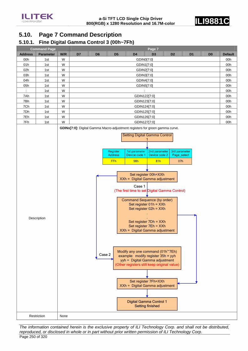
a-Si TFT LCD Single Chip Driver 800(RGB) x 1280 Resolution and 16.7M-color ILI9881C
The information contained herein is the exclusive property of ILI Technology Corp. and shall not be distributed, reproduced, or disclosed in whole or in part without prior written permission of ILI Technology Corp. Page 250 of 320
5.10. Page 7 Command Description
5.10.1. Fine Digital Gamma Control 3 (00h~7Fh)
Command Page Page 7
Address Parameter W/R D7 D6 D5 D4 D3 D2 D1 D0 Default
00h 1st W GDIN0[7:0] 00h
01h 1st W GDIN1[7:0] 00h
02h 1st W GDIN2[7:0] 00h
03h 1st W GDIN3[7:0] 00h
04h 1st W GDIN4[7:0] 00h
05h 1st W GDIN5[7:0] 00h
: 1st W : 00h
7Ah 1st W GDIN122[7:0] 00h
7Bh 1st W GDIN123[7:0] 00h
7Ch 1st W GDIN124[7:0] 00h
7Dh 1st W GDIN125[7:0] 00h
7Eh 1st W GDIN126[7:0] 00h
7Fh 1st W GDIN127[7:0] 00h
Description
GDINx[7:0]: Digital Gamma Macro-adjustment registers for green gamma curve.
Setting Digital Gamma Control
1
Set register 00h=XXh
XXh = Digital Gamma adjustment
Command Sequence (by order)
Set register 01h = XXh
Set register 02h = XXh
.
.
Set register 7Dh = XXh
Set register 7Eh = XXh
XXh = Digital Gamma adjustment
Set register 7Fh=XXh
XXh = Digital Gamma adjustment
Modify any one command (01h~7Eh)
example: modify register 35h = yyh
yyh = Digital Gamma adjustment
(Other registers still keep original value)
Digital Gamma Control 1
Setting finished
Case 1
Case 2
(The first time to set Digital Gamma Control)
Register
Address
FFh
1st parameter
Device code 1
98h
2nd parameter
Device code 2
81h
3rd parameter
Page_select
07h
Restriction None

a-Si TFT LCD Single Chip Driver 800(RGB) x 1280 Resolution and 16.7M-color ILI9881C
The information contained herein is the exclusive property of ILI Technology Corp. and shall not be distributed, reproduced, or disclosed in whole or in part without prior written permission of ILI Technology Corp. Page 251 of 320
Register
Availability
Status Availability
Normal Mode On, Idle Mode Off, Sleep Out Yes
Normal Mode On, Idle Mode On, Sleep Out Yes
Sleep In Yes
Default
Status Default Value
Power On Sequence 00h_00h_...00h_00h
S/W Reset 00h_00h_...00h_00h
H/W Reset 00h_00h_...00h_00h

a-Si TFT LCD Single Chip Driver 800(RGB) x 1280 Resolution and 16.7M-color ILI9881C
The information contained herein is the exclusive property of ILI Technology Corp. and shall not be distributed, reproduced, or disclosed in whole or in part without prior written permission of ILI Technology Corp. Page 252 of 320
5.10.2. EXTC Command Set Enable Register (FFh)
Command Page Page 7
Address Parameter W/R D7 D6 D5 D4 D3 D2 D1 D0 Default
FFh
1st W 1 0 0 1 1 0 0 0 98h
2nd W 1 0 0 0 0 0 0 1 81h
3rd W PAGE[7:0] 07h
Description
PAGE[7:0]: Set the command page.
PAGE[7:0] Command Page
00h Page 0
01h Page 1
02h Page 2
03h Page 3
04h Page 4
05h Page 5
06h Page 6
07h Page 7
08h Page 8
09h Page 9
0Ah Page 10
Others Reserved
Set the register, 1st Parameter = 98h, 2
nd Parameter = 81h, 3
rd Parameter = Page value to enable “Page command set”
available
See section “5.1 Command Flow”.
Restriction None
Register
Availability
Status Availability
Normal Mode On, Idle Mode Off, Sleep Out Yes
Normal Mode On, Idle Mode On, Sleep Out Yes
Sleep In Yes
Default
Status Default Value
Power On Sequence 07h
S/W Reset 07h
H/W Reset 07h

a-Si TFT LCD Single Chip Driver 800(RGB) x 1280 Resolution and 16.7M-color ILI9881C
The information contained herein is the exclusive property of ILI Technology Corp. and shall not be distributed, reproduced, or disclosed in whole or in part without prior written permission of ILI Technology Corp. Page 253 of 320
5.11. Page 8 Command Description
5.11.1. Fine Digital Gamma Control 4 (00h~7Fh)
Command Page Page 8
Address Parameter W/R D7 D6 D5 D4 D3 D2 D1 D0 Default
00h 1st W GDIN128[7:0] 00h
01h 1st W GDIN129[7:0] 00h
02h 1st W GDIN130[7:0] 00h
03h 1st W GDIN131[7:0] 00h
04h 1st W GDIN132[7:0] 00h
05h 1st W GDIN133[7:0] 00h
: 1st W : 00h
7Ah 1st W GDIN250[7:0] 00h
7Bh 1st W GDIN251[7:0] 00h
7Ch 1st W GDIN252[7:0] 00h
7Dh 1st W GDIN253[7:0] 00h
7Eh 1st W GDIN254[7:0] 00h
7Fh 1st W GDIN255[7:0] 00h
Description
GDINx[7:0]: Digital Gamma Macro-adjustment registers for green gamma curve.
Setting Digital Gamma Control 1
Set register 00h=XXh
XXh = Digital Gamma adjustment
Command Sequence (by order)
Set register 01h = XXh
Set register 02h = XXh
.
.
Set register 7Dh = XXh
Set register 7Eh = XXh
XXh = Digital Gamma adjustment
Set register 7Fh=XXh
XXh = Digital Gamma adjustment
Modify any one command (01h~7Eh)
example: modify register 35h = yyh
yyh = Digital Gamma adjustment
(Other registers still keep original value)
Digital Gamma Control 1
Setting finished
Case 1
Case 2
(The first time to set Digital Gamma Control)
Register
Address
FFh
1st parameter
Device code 1
98h
2nd parameter
Device code 2
81h
3rd parameter
Page_select
08h
Restriction None

a-Si TFT LCD Single Chip Driver 800(RGB) x 1280 Resolution and 16.7M-color ILI9881C
The information contained herein is the exclusive property of ILI Technology Corp. and shall not be distributed, reproduced, or disclosed in whole or in part without prior written permission of ILI Technology Corp. Page 254 of 320
Register
Availability
Status Availability
Normal Mode On, Idle Mode Off, Sleep Out Yes
Normal Mode On, Idle Mode On, Sleep Out Yes
Sleep In Yes
Default
Status Default Value
Power On Sequence 00h_00h_...00h_00h
S/W Reset 00h_00h_...00h_00h
H/W Reset 00h_00h_...00h_00h

a-Si TFT LCD Single Chip Driver 800(RGB) x 1280 Resolution and 16.7M-color ILI9881C
The information contained herein is the exclusive property of ILI Technology Corp. and shall not be distributed, reproduced, or disclosed in whole or in part without prior written permission of ILI Technology Corp. Page 255 of 320
5.11.2. EXTC Command Set Enable Register (FFh)
Command Page Page 8
Address Parameter W/R D7 D6 D5 D4 D3 D2 D1 D0 Default
FFh
1st W 1 0 0 1 1 0 0 0 98h
2nd W 1 0 0 0 0 0 0 1 81h
3rd W PAGE[7:0] 08h
Description
PAGE[7:0]: Set the command page.
PAGE[7:0] Command Page
00h Page 0
01h Page 1
02h Page 2
03h Page 3
04h Page 4
05h Page 5
06h Page 6
07h Page 7
08h Page 8
09h Page 9
0Ah Page 10
Others Reserved
Set the register, 1st Parameter = 98h, 2
nd Parameter = 81h, 3
rd Parameter = Page value to enable “Page command set”
available
See section “5.1 Command Flow”.
Restriction None
Register
Availability
Status Availability
Normal Mode On, Idle Mode Off, Sleep Out Yes
Normal Mode On, Idle Mode On, Sleep Out Yes
Sleep In Yes
Default
Status Default Value
Power On Sequence 08h
S/W Reset 08h
H/W Reset 08h

a-Si TFT LCD Single Chip Driver 800(RGB) x 1280 Resolution and 16.7M-color ILI9881C
The information contained herein is the exclusive property of ILI Technology Corp. and shall not be distributed, reproduced, or disclosed in whole or in part without prior written permission of ILI Technology Corp. Page 256 of 320
5.12. Page 9 Command Description
5.12.1. Fine Digital Gamma Control 5 (00h~7Fh)
Command Page Page 9
Address Parameter W/R D7 D6 D5 D4 D3 D2 D1 D0 Default
00h 1st W BDIN0[7:0] 00h
01h 1st W BDIN1[7:0] 00h
02h 1st W BDIN2[7:0] 00h
03h 1st W BDIN3[7:0] 00h
04h 1st W BDIN4[7:0] 00h
05h 1st W BDIN5[7:0] 00h
: 1st W : 00h
7Ah 1st W BDIN122[7:0] 00h
7Bh 1st W BDIN123[7:0] 00h
7Ch 1st W BDIN124[7:0] 00h
7Dh 1st W BDIN125[7:0] 00h
7Eh 1st W BDIN126[7:0] 00h
7Fh 1st W BDIN127[7:0] 00h
Description
BDINx[7:0]: Digital Gamma Macro-adjustment registers for blue gamma curve.
Setting Digital Gamma Control 1
Set register 00h=XXh
XXh = Digital Gamma adjustment
Command Sequence (by order)
Set register 01h = XXh
Set register 02h = XXh
.
.
Set register 7Dh = XXh
Set register 7Eh = XXh
XXh = Digital Gamma adjustment
Set register 7Fh=XXh
XXh = Digital Gamma adjustment
Modify any one command (01h~7Eh)
example: modify register 35h = yyh
yyh = Digital Gamma adjustment
(Other registers still keep original value)
Digital Gamma Control 1
Setting finished
Case 1
Case 2
(The first time to set Digital Gamma Control)
Register
Address
FFh
1st parameter
Device code 1
98h
2nd parameter
Device code 2
81h
3rd parameter
Page_select
09h
Restriction None
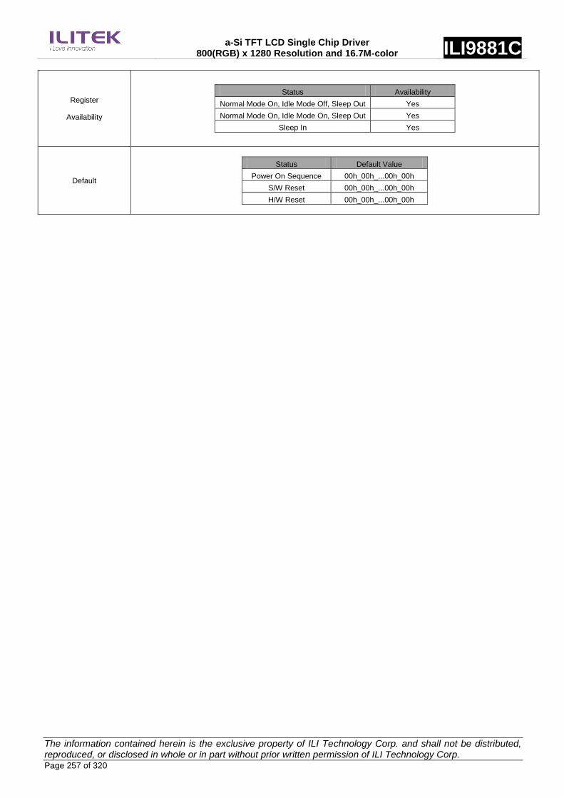
a-Si TFT LCD Single Chip Driver 800(RGB) x 1280 Resolution and 16.7M-color ILI9881C
The information contained herein is the exclusive property of ILI Technology Corp. and shall not be distributed, reproduced, or disclosed in whole or in part without prior written permission of ILI Technology Corp. Page 257 of 320
Register
Availability
Status Availability
Normal Mode On, Idle Mode Off, Sleep Out Yes
Normal Mode On, Idle Mode On, Sleep Out Yes
Sleep In Yes
Default
Status Default Value
Power On Sequence 00h_00h_...00h_00h
S/W Reset 00h_00h_...00h_00h
H/W Reset 00h_00h_...00h_00h
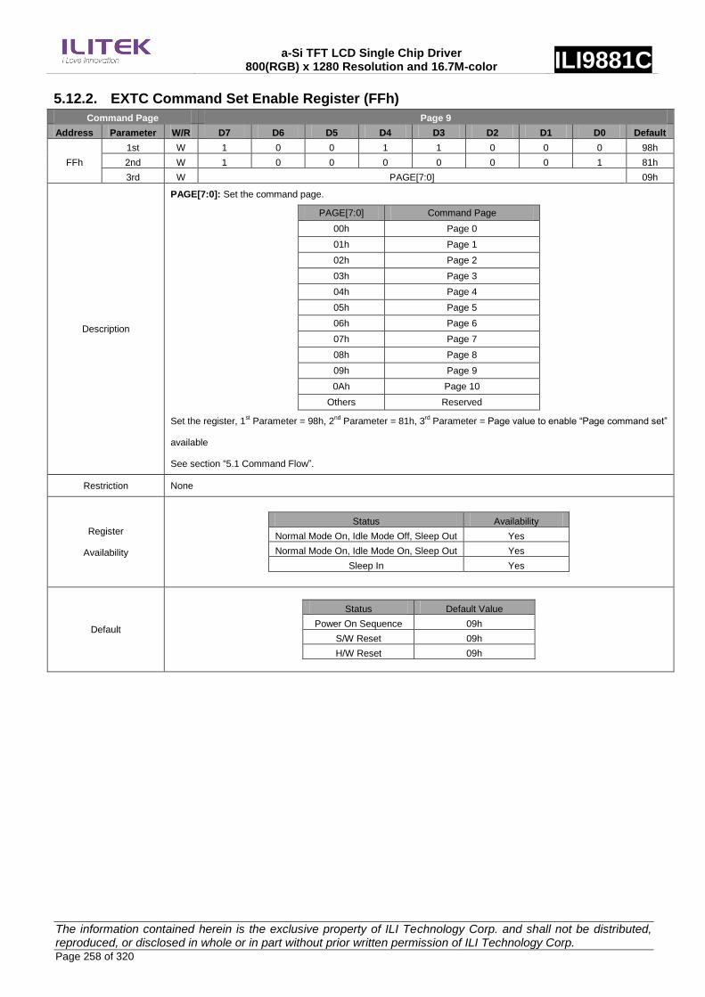
a-Si TFT LCD Single Chip Driver 800(RGB) x 1280 Resolution and 16.7M-color ILI9881C
The information contained herein is the exclusive property of ILI Technology Corp. and shall not be distributed, reproduced, or disclosed in whole or in part without prior written permission of ILI Technology Corp. Page 258 of 320
5.12.2. EXTC Command Set Enable Register (FFh)
Command Page Page 9
Address Parameter W/R D7 D6 D5 D4 D3 D2 D1 D0 Default
FFh
1st W 1 0 0 1 1 0 0 0 98h
2nd W 1 0 0 0 0 0 0 1 81h
3rd W PAGE[7:0] 09h
Description
PAGE[7:0]: Set the command page.
PAGE[7:0] Command Page
00h Page 0
01h Page 1
02h Page 2
03h Page 3
04h Page 4
05h Page 5
06h Page 6
07h Page 7
08h Page 8
09h Page 9
0Ah Page 10
Others Reserved
Set the register, 1st Parameter = 98h, 2
nd Parameter = 81h, 3
rd Parameter = Page value to enable “Page command set”
available
See section “5.1 Command Flow”.
Restriction None
Register
Availability
Status Availability
Normal Mode On, Idle Mode Off, Sleep Out Yes
Normal Mode On, Idle Mode On, Sleep Out Yes
Sleep In Yes
Default
Status Default Value
Power On Sequence 09h
S/W Reset 09h
H/W Reset 09h

a-Si TFT LCD Single Chip Driver 800(RGB) x 1280 Resolution and 16.7M-color ILI9881C
The information contained herein is the exclusive property of ILI Technology Corp. and shall not be distributed, reproduced, or disclosed in whole or in part without prior written permission of ILI Technology Corp. Page 259 of 320
5.13. Page 10 Command Description
5.13.1. Fine Digital Gamma Control 6 (00h~7Fh)
Command Page Page 10
Address Parameter W/R D7 D6 D5 D4 D3 D2 D1 D0 Default
00h 1st W BDIN128[7:0] 00h
01h 1st W BDIN129[7:0] 00h
02h 1st W BDIN130[7:0] 00h
03h 1st W BDIN131[7:0] 00h
04h 1st W BDIN132[7:0] 00h
05h 1st W BDIN133[7:0] 00h
: 1st W : 00h
7Ah 1st W BDIN250[7:0] 00h
7Bh 1st W BDIN251[7:0] 00h
7Ch 1st W BDIN252[7:0] 00h
7Dh 1st W BDIN253[7:0] 00h
7Eh 1st W BDIN254[7:0] 00h
7Fh 1st W BDIN255[7:0] 00h
Description
BDINx[7:0]: Digital Gamma Macro-adjustment registers for blue gamma curve.
Setting Digital Gamma Control 1
Set register 00h=XXh
XXh = Digital Gamma adjustment
Command Sequence (by order)
Set register 01h = XXh
Set register 02h = XXh
.
.
Set register 7Dh = XXh
Set register 7Eh = XXh
XXh = Digital Gamma adjustment
Set register 7Fh=XXh
XXh = Digital Gamma adjustment
Modify any one command (01h~7Eh)
example: modify register 35h = yyh
yyh = Digital Gamma adjustment
(Other registers still keep original value)
Digital Gamma Control 1
Setting finished
Case 1
Case 2
(The first time to set Digital Gamma Control)
Register
Address
FFh
1st parameter
Device code 1
98h
2nd parameter
Device code 2
81h
3rd parameter
Page_select
0Ah
Restriction None

a-Si TFT LCD Single Chip Driver 800(RGB) x 1280 Resolution and 16.7M-color ILI9881C
The information contained herein is the exclusive property of ILI Technology Corp. and shall not be distributed, reproduced, or disclosed in whole or in part without prior written permission of ILI Technology Corp. Page 260 of 320
Register
Availability
Status Availability
Normal Mode On, Idle Mode Off, Sleep Out Yes
Normal Mode On, Idle Mode On, Sleep Out Yes
Sleep In Yes
Default
Status Default Value
Power On Sequence 00h_00h_...00h_00h
S/W Reset 00h_00h_...00h_00h
H/W Reset 00h_00h_...00h_00h

a-Si TFT LCD Single Chip Driver 800(RGB) x 1280 Resolution and 16.7M-color ILI9881C
The information contained herein is the exclusive property of ILI Technology Corp. and shall not be distributed, reproduced, or disclosed in whole or in part without prior written permission of ILI Technology Corp. Page 261 of 320
5.13.2. EXTC Command Set Enable Register (FFh)
Command Page Page 10
Address Parameter W/R D7 D6 D5 D4 D3 D2 D1 D0 Default
FFh
1st W 1 0 0 1 1 0 0 0 98h
2nd W 1 0 0 0 0 0 0 1 81h
3rd W PAGE[7:0] 0Ah
Description
PAGE[7:0]: Set the command page.
PAGE[7:0] Command Page
00h Page 0
01h Page 1
02h Page 2
03h Page 3
04h Page 4
05h Page 5
06h Page 6
07h Page 7
08h Page 8
09h Page 9
0Ah Page 10
Others Reserved
Set the register, 1st Parameter = 98h, 2
nd Parameter = 81h, 3
rd Parameter = Page value to enable “Page command set”
available
See section “5.1 Command Flow”.
Restriction None
Register
Availability
Status Availability
Normal Mode On, Idle Mode Off, Sleep Out Yes
Normal Mode On, Idle Mode On, Sleep Out Yes
Sleep In Yes
Default
Status Default Value
Power On Sequence 0Ah
S/W Reset 0Ah
H/W Reset 0Ah

a-Si TFT LCD Single Chip Driver 800(RGB) x 1280 Resolution and 16.7M-color ILI9881C
The information contained herein is the exclusive property of ILI Technology Corp. and shall not be distributed, reproduced, or disclosed in whole or in part without prior written permission of ILI Technology Corp. Page 262 of 320
6. Source Driver
The source driver uses 2402 channels (S1~S2400 and SDUM[2:1] channels) for the Zig-zag function used for
driving the source line of the TFT LCD panel. The source driver converts the digital data into the analog voltage
and generates corresponding gray scale voltage output, enabling up to 16.7M colors to be displayed
simultaneously. The output circuit of this source driver incorporates an operational amplifier, so that a positive and
a negative voltage can be alternately outputted from each channel.
6.1. Zig-zag Inversion Zig-zag Inversion is used to reduce the power consumption. The Zig-zag inversion decreases the switching
frequency of the source related to the magnitude of power consumption. This method will have an addendum data
line, SDUM.
-+ + -
+- - +
-+ + -
Pixel Charging
Waveform
VCOM VCOM VCOM
+ - + - + -
Sn-1 Sn Sn+1
Gn-1
Gn
Gn+1
Gate
1-Dot Inversion Driving
-+ + -
+- - +
-+ + -
Pixel Charging
Waveform
VCOM VCOM VCOM
+ - + - + -
Sn-1 Sn Sn+1
Gn-1
Gn
Gn+1
Gate
Vertical Bi-Color driving

a-Si TFT LCD Single Chip Driver 800(RGB) x 1280 Resolution and 16.7M-color ILI9881C
The information contained herein is the exclusive property of ILI Technology Corp. and shall not be distributed, reproduced, or disclosed in whole or in part without prior written permission of ILI Technology Corp. Page 263 of 320
6.2. Zig-zag Inversion Concept The Zig-zag method uses the same polarity of data line of the column inversion to show the 1-dot inversion.
SDUM1 S1 S2 S3 Sn-3 Sn-2 Sn-1 Sn
Gate # 1
Gate # 3
Gate # 2
Gate # 4
...
...
...
...
+
+
+
+
+
+
+
+
+
+
+
+
+
+
+
-
-
-
-
-
-
-
-
-
-
-
-
-
-
-
-
-
-
-
-
Vcom Vcom Vcom Vcom Vcom Vcom Vcom
Vdata
(Neg.)
Vdata
(Pos.)
Vdata
(Neg.)
Vdata
(Pos.)
Vdata
(Neg.)
Vdata
(Pos.)
Vdata
(Neg.)
...
Column Inversion
- + - + - +
+ - + - + -
- + - + - +
+ - + - + -
...
...
...
...
1-Dot Inversion
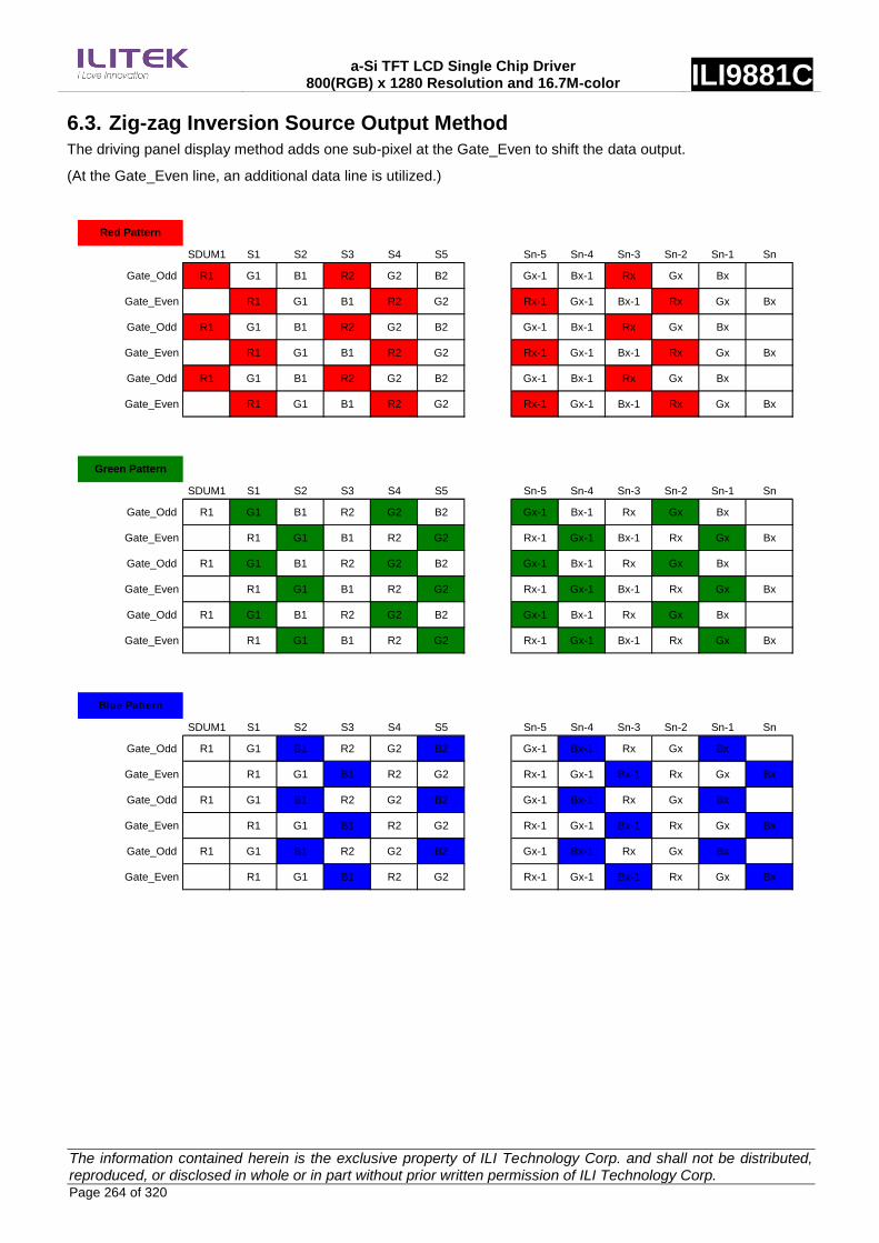
a-Si TFT LCD Single Chip Driver 800(RGB) x 1280 Resolution and 16.7M-color ILI9881C
The information contained herein is the exclusive property of ILI Technology Corp. and shall not be distributed, reproduced, or disclosed in whole or in part without prior written permission of ILI Technology Corp. Page 264 of 320
6.3. Zig-zag Inversion Source Output Method The driving panel display method adds one sub-pixel at the Gate_Even to shift the data output.
(At the Gate_Even line, an additional data line is utilized.)
SDUM1 S1 S2 S3 S4 S5 Sn-5 Sn-4 Sn-3 Sn-2 Sn-1 Sn
Gate_Odd R1 G1 B1 R2 G2 B2 Gx-1 Bx-1 Rx Gx Bx
Gate_Even R1 G1 B1 R2 G2 Rx-1 Gx-1 Bx-1 Rx Gx Bx
Gate_Odd R1 G1 B1 R2 G2 B2 Gx-1 Bx-1 Rx Gx Bx
Gate_Even R1 G1 B1 R2 G2 Rx-1 Gx-1 Bx-1 Rx Gx Bx
Gate_Odd R1 G1 B1 R2 G2 B2 Gx-1 Bx-1 Rx Gx Bx
Gate_Even R1 G1 B1 R2 G2 Rx-1 Gx-1 Bx-1 Rx Gx Bx
Red Pattern
Green Pattern
Blue Pattern

a-Si TFT LCD Single Chip Driver 800(RGB) x 1280 Resolution and 16.7M-color ILI9881C
The information contained herein is the exclusive property of ILI Technology Corp. and shall not be distributed, reproduced, or disclosed in whole or in part without prior written permission of ILI Technology Corp. Page 265 of 320
6.4. Zig-zag Inversion RED Data Display The figure below illustrates the Zig-zag inversion panel driving method for Red data input.
When driving a Red pattern, the Red and Blue sub-pixels will light up line by line according to the data signal input.
R G B R G B
R G B R G B
R G B R G B
R G B R G B
Gate_Odd
Gate_Odd
Gate_Even
Gate_Even
...
...
...
...
R G B R G B
R G B R G B
R G B R G B
R G B R G B
SDUM1 S1 S2 S3 S4 S5 S6 Sn-6 Sn-5 Sn-4 Sn-3 Sn-2 Sn-1 Sn
Source Output
Panel Driving
SDUM1 S1 S2 S3 S4 S5 S6 Sn-6 Sn-5 Sn-4 Sn-3 Sn-2 Sn-1 Sn
Gate_Odd R1 G1 B1 R2 G2 B2 R3 Rx-1 Gx-1 Bx-1 Rx Gx Bx
Gate_Even R1 G1 B1 R2 G2 B2 Bx-2 Rx-1 Gx-1 Bx-1 Rx Gx Bx
Gate_Odd R1 G1 B1 R2 G2 B2 R3 … Rx-1 Gx-1 Bx-1 Rx Gx Bx
Gate_Even R1 G1 B1 R2 G2 B2 Bx-2 Rx-1 Gx-1 Bx-1 Rx Gx Bx
The figure below is the Zig-zag inversion panel driving method. The panel will be driven by the Red data input of
the Gate_Odd and the Green data input of the Gate_Even.
R G B R G B
R G B R G B
R G B R G B
R G B R G B
Gate_Odd
Gate_Odd
Gate_Even
Gate_Even
...
...
...
...
R G B R G B
R G B R G B
R G B R G B
R G B R G B
SDUM1 S1 S2 S3 S4 S5 S6 SN-6 Sn-5 Sn-4 Sn-3 Sn-2 Sn-1 Sn
Source Output
Panel Driving
SDUM1 S1 S2 S3 S4 S5 S6 Sn-6 Sn-5 Sn-4 Sn-3 Sn-2 Sn-1 Sn
Gate_Odd R1 G1 B1 R2 G2 B2 R3 Rx-1 Gx-1 Bx-1 Rx Gx Bx
Gate_Even R1 G1 B1 R2 G2 B2 Bx-2 Rx-1 Gx-1 Bx-1 Rx Gx Bx
Gate_Odd R1 G1 B1 R2 G2 B2 R3 … Rx-1 Gx-1 Bx-1 Rx Gx Bx
Gate_Even R1 G1 B1 R2 G2 B2 Bx-2 Rx-1 Gx-1 Bx-1 Rx Gx Bx

a-Si TFT LCD Single Chip Driver 800(RGB) x 1280 Resolution and 16.7M-color ILI9881C
The information contained herein is the exclusive property of ILI Technology Corp. and shall not be distributed, reproduced, or disclosed in whole or in part without prior written permission of ILI Technology Corp. Page 266 of 320
6.5. Zig-zag Inversion GREEN Data Display The figure below illustrates the Zig-zag inversion panel driving method for Green data input.
When driving a Green pattern, the Green and Red sub-pixels will light up line by line according to the data signal
input.
R G B R G B
R G B R G B
R G B R G B
R G B R G B
Gate_Odd
Gate_Odd
Gate_Even
Gate_Even
...
...
...
...
R G B R G B
R G B R G B
R G B R G B
R G B R G B
SDUM1 S1 S2 S3 S4 S5 S6 SN-6 Sn-5 Sn-4 Sn-3 Sn-2 Sn-1 Sn
Source Output
Panel Driving
SDUM1 S1 S2 S3 S4 S5 S6 Sn-6 Sn-5 Sn-4 Sn-3 Sn-2 Sn-1 Sn
Gate_Odd R1 G1 B1 R2 G2 B2 R3 Rx-1 Gx-1 Bx-1 Rx Gx Bx
Gate_Even R1 G1 B1 R2 G2 B2 Bx-2 Rx-1 Gx-1 Bx-1 Rx Gx Bx
Gate_Odd R1 G1 B1 R2 G2 B2 R3 … Rx-1 Gx-1 Bx-1 Rx Gx Bx
Gate_Even R1 G1 B1 R2 G2 B2 Bx-2 Rx-1 Gx-1 Bx-1 Rx Gx Bx
The figure below is the Zig-zag inversion panel driving method. The panel will be driven by the Green data input of
the Gate_Odd and the Blue data input of the Gate_Even.
R G B R G B
R G B R G B
R G B R G B
R G B R G B
Gate_Odd
Gate_Odd
Gate_Even
Gate_Even
...
...
...
...
R G B R G B
R G B R G B
R G B R G B
R G B R G B
SDUM1 S1 S2 S3 S4 S5 S6 SN-6 Sn-5 Sn-4 Sn-3 Sn-2 Sn-1 Sn
Source Output
Panel Driving
SDUM1 S1 S2 S3 S4 S5 S6 Sn-6 Sn-5 Sn-4 Sn-3 Sn-2 Sn-1 Sn
Gate_Odd R1 G1 B1 R2 G2 B2 R3 Rx-1 Gx-1 Bx-1 Rx Gx Bx
Gate_Even R1 G1 B1 R2 G2 B2 Bx-2 Rx-1 Gx-1 Bx-1 Rx Gx Bx
Gate_Odd R1 G1 B1 R2 G2 B2 R3 … Rx-1 Gx-1 Bx-1 Rx Gx Bx
Gate_Even R1 G1 B1 R2 G2 B2 Bx-2 Rx-1 Gx-1 Bx-1 Rx Gx Bx

a-Si TFT LCD Single Chip Driver 800(RGB) x 1280 Resolution and 16.7M-color ILI9881C
The information contained herein is the exclusive property of ILI Technology Corp. and shall not be distributed, reproduced, or disclosed in whole or in part without prior written permission of ILI Technology Corp. Page 267 of 320
6.6. Zig-zag Inversion BLUE Data Display The figure below illustrates the Zig-zag inversion panel driving method for Blue data input.
When driving a Blue pattern, the Blue and Green sub-pixels will light up line by line according to the data signal
input.
R G B R G B
R G B R G B
R G B R G B
R G B R G B
Gate_Odd
Gate_Odd
Gate_Even
Gate_Even
...
...
...
...
R G B R G B
R G B R G B
R G B R G B
R G B R G B
SDUM1 S1 S2 S3 S4 S5 S6 SN-6 Sn-5 Sn-4 Sn-3 Sn-2 Sn-1 Sn
Source Output
Panel Driving
SDUM1 S1 S2 S3 S4 S5 S6 Sn-6 Sn-5 Sn-4 Sn-3 Sn-2 Sn-1 Sn
Gate_Odd R1 G1 B1 R2 G2 B2 R3 Rx-1 Gx-1 Bx-1 Rx Gx Bx
Gate_Even R1 G1 B1 R2 G2 B2 Bx-2 Rx-1 Gx-1 Bx-1 Rx Gx Bx
Gate_Odd R1 G1 B1 R2 G2 B2 R3 … Rx-1 Gx-1 Bx-1 Rx Gx Bx
Gate_Even R1 G1 B1 R2 G2 B2 Bx-2 Rx-1 Gx-1 Bx-1 Rx Gx Bx
The figure below is the Zig-zag inversion panel driving method. The panel will be driven by the Blue data input of
the Gate_Odd and the Red data input of the Gate_Even.
R G B R G B
R G B R G B
R G B R G B
R G B R G B
Gate_Odd
Gate_Odd
Gate_Even
Gate_Even
...
...
...
...
R G B R G B
R G B R G B
R G B R G B
R G B R G B
SDUM1 S1 S2 S3 S4 S5 S6 SN-6 Sn-5 Sn-4 Sn-3 Sn-2 Sn-1 Sn
Source Output
Panel Driving
SDUM1 S1 S2 S3 S4 S5 S6 Sn-6 Sn-5 Sn-4 Sn-3 Sn-2 Sn-1 Sn
Gate_Odd R1 G1 B1 R2 G2 B2 R3 Rx-1 Gx-1 Bx-1 Rx Gx Bx
Gate_Even R1 G1 B1 R2 G2 B2 Bx-2 Rx-1 Gx-1 Bx-1 Rx Gx Bx
Gate_Odd R1 G1 B1 R2 G2 B2 R3 … Rx-1 Gx-1 Bx-1 Rx Gx Bx
Gate_Even R1 G1 B1 R2 G2 B2 Bx-2 Rx-1 Gx-1 Bx-1 Rx Gx Bx

a-Si TFT LCD Single Chip Driver 800(RGB) x 1280 Resolution and 16.7M-color ILI9881C
The information contained herein is the exclusive property of ILI Technology Corp. and shall not be distributed, reproduced, or disclosed in whole or in part without prior written permission of ILI Technology Corp. Page 268 of 320
6.7. Different Zig-zag Type Panel
Zig-zag Type 1 (NLA[3:0] = 9h)
1 2 3 1438 1439 1440
2 3 4 1439 1440 1441
1 2 3 1438 1439 1440
2 3 4 1439 1440 1441
SDUM1 S1 S2 S3 S2397 S2398 S2399 S2400
Gate # 1
Gate # 3
Gate # 2
Gate # 4
...
...
...
...
Zig-zag Type 2 (NLA[3:0] = Ah)
1 2 3 1438 1439 1440
2 3 4 1439 1440 1441
1 2 3 1438 1439 1440
2 3 4 1439 1440 1441
SDUM1 S1 S2 S3 S2397 S2398 S2399 S2400
Gate # 4
Gate # 2
Gate # 1
Gate # 3
...
...
...
...

a-Si TFT LCD Single Chip Driver 800(RGB) x 1280 Resolution and 16.7M-color ILI9881C
The information contained herein is the exclusive property of ILI Technology Corp. and shall not be distributed, reproduced, or disclosed in whole or in part without prior written permission of ILI Technology Corp. Page 269 of 320
Zig-zag Type 3 (NLA[3:0] = Bh)
2 3 4 1439 1440 1441
1 2 3 1438 1439 1440
2 3 4 1439 1440 1441
S1 S2 S3 S4 S2398 S2399 S2400 SDUM2
Gate # 1
Gate # 3
Gate # 2
Gate # 4
...
...
...
1 2 3 1438 1439 1440...
Zig-zag Type 4 (NLA[3:0] = Ch)
2 3 4 1439 1440 1441
1 2 3 1438 1439 1440
2 3 4 1439 1440 1441
S1 S2 S3 S4 S2398 S2399 S2400 SDUM2
Gate # 4
Gate # 2
Gate # 1
Gate # 3
...
...
...
1 2 3 1438 1439 1440...
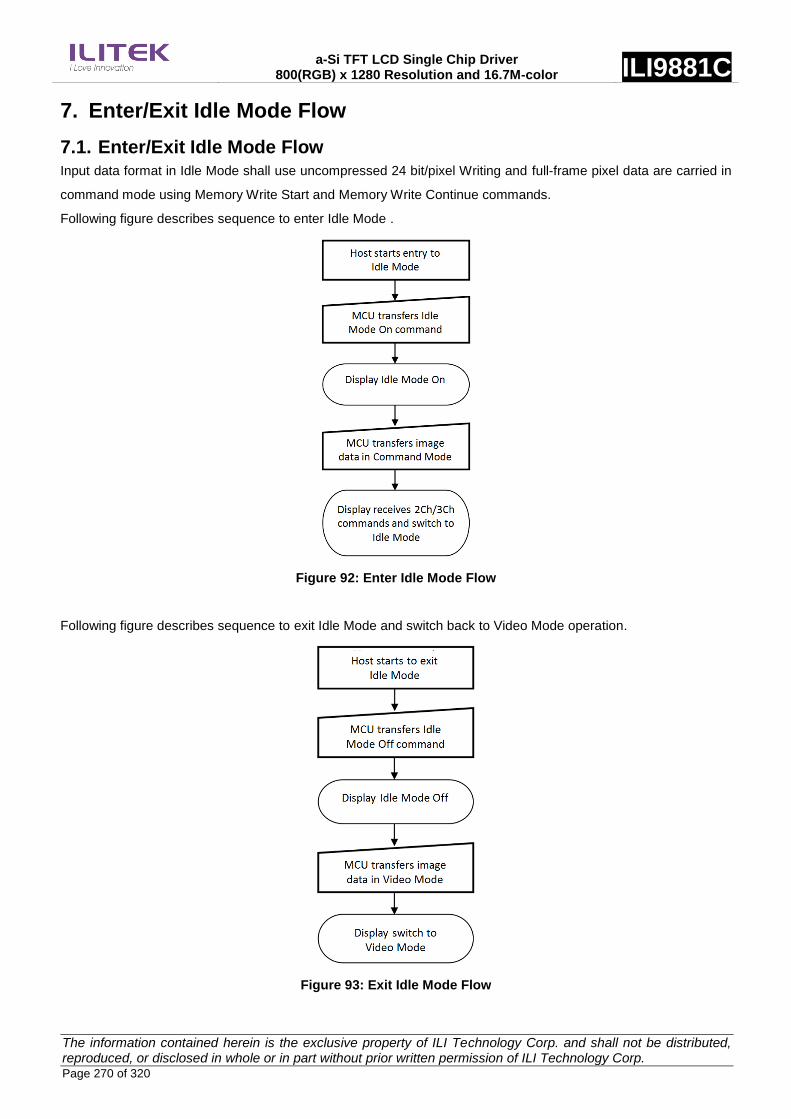
a-Si TFT LCD Single Chip Driver 800(RGB) x 1280 Resolution and 16.7M-color ILI9881C
The information contained herein is the exclusive property of ILI Technology Corp. and shall not be distributed, reproduced, or disclosed in whole or in part without prior written permission of ILI Technology Corp. Page 270 of 320
7. Enter/Exit Idle Mode Flow
7.1. Enter/Exit Idle Mode Flow Input data format in Idle Mode shall use uncompressed 24 bit/pixel Writing and full-frame pixel data are carried in
command mode using Memory Write Start and Memory Write Continue commands.
Following figure describes sequence to enter Idle Mode .
Figure 92: Enter Idle Mode Flow
Following figure describes sequence to exit Idle Mode and switch back to Video Mode operation.
Figure 93: Exit Idle Mode Flow
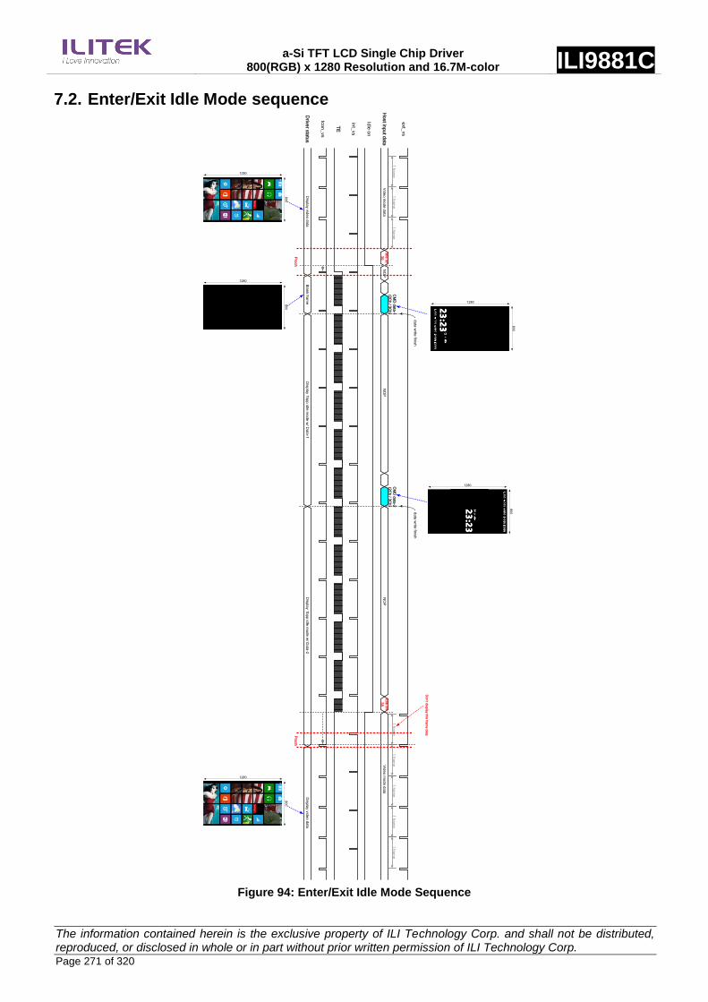
a-Si TFT LCD Single Chip Driver 800(RGB) x 1280 Resolution and 16.7M-color ILI9881C
The information contained herein is the exclusive property of ILI Technology Corp. and shall not be distributed, reproduced, or disclosed in whole or in part without prior written permission of ILI Technology Corp. Page 271 of 320
7.2. Enter/Exit Idle Mode sequence
1 fra
me
1 fra
me
1 fra
me
Vid
eo
mo
de
da
taId
le o
n
39
CM
D d
ata
-1
(2C
h / 3
Ch
)
NO
PH
ost in
pu
t da
ta
Driv
er s
tatu
s
TE
Dis
pla
y v
ide
o d
ata
Bla
nk fra
me
Dis
pla
y 1
bp
p id
le m
od
e w
/ Da
ta-1
da
ta w
rite fin
ish
Idle
on
Vid
eo
mo
de
da
ta
1 fra
me
1 fra
me
1 fra
me
1 fra
me
1 fra
me
Dis
pla
y v
ide
o d
ata
ext_
vs
int_
vs
Idle
off
38
NO
P
tco
n_
vs
Dis
pla
y 1
bp
p id
le m
od
e w
/ Da
ta-2
80
0
1280
80
0
1280
80
0
1280
CM
D d
ata
-2
(2C
h / 3
Ch
)
da
ta w
rite fin
ish
NO
P
80
0
1280
80
0
1280
Pro
ch
Pro
ch
Do
n’t d
isp
lay th
is fra
me
da
ta
Figure 94: Enter/Exit Idle Mode Sequence
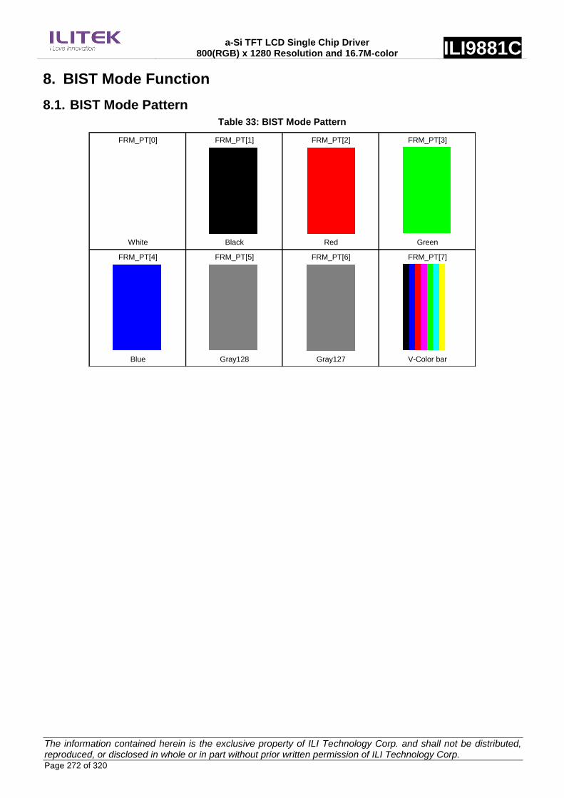
a-Si TFT LCD Single Chip Driver 800(RGB) x 1280 Resolution and 16.7M-color ILI9881C
The information contained herein is the exclusive property of ILI Technology Corp. and shall not be distributed, reproduced, or disclosed in whole or in part without prior written permission of ILI Technology Corp. Page 272 of 320
8. BIST Mode Function
8.1. BIST Mode Pattern
Table 33: BIST Mode Pattern
FRM_PT[0] FRM_PT[1] FRM_PT[2] FRM_PT[3]
White Black Red Green
FRM_PT[4] FRM_PT[5] FRM_PT[6] FRM_PT[7]
Blue Gray128 Gray127 V-Color bar

a-Si TFT LCD Single Chip Driver 800(RGB) x 1280 Resolution and 16.7M-color ILI9881C
The information contained herein is the exclusive property of ILI Technology Corp. and shall not be distributed, reproduced, or disclosed in whole or in part without prior written permission of ILI Technology Corp. Page 273 of 320
9. Content Adaptive Brightness Control (CABC) Function
The CABC, a dynamic backlight control function, drastically reduces the power consumption of the luminance
source. The ILI9881C will refer the gray scale content of the display image to output in PWM waveform then to the
LED driver for backlight brightness control. The content of gray scale can be increased while simultaneously
lowering the brightness of the backlight to achieve the same perceived brightness. The adjusted gray level scale
and the power consumption reduction depend on the content of the image.
LED LEDLED
LEDPWMHistogram
Analysis
Gain
Control
Image Data
BL
Control
PWM
Generator
Data
Control
SRC
Driver
LED
Driver
Panel
Figure 95: CABC Block Diagram
The ILI9881C can calculate the backlight brightness level and send a PWM_OUT pulse to the LED driver via
LEDPWM pin for backlight brightness control purposes. The PWM frequency can be adjusted by PWM_DIV
parameters, and the calculating equation is shown below:
Figure 96 is the basic timing diagram which is applied from the ILI9881C in order to control the LED driver.
tperiod
tontoff
LEDPWM
CABC ON
Figure 96: PWM OUT On/Off Period
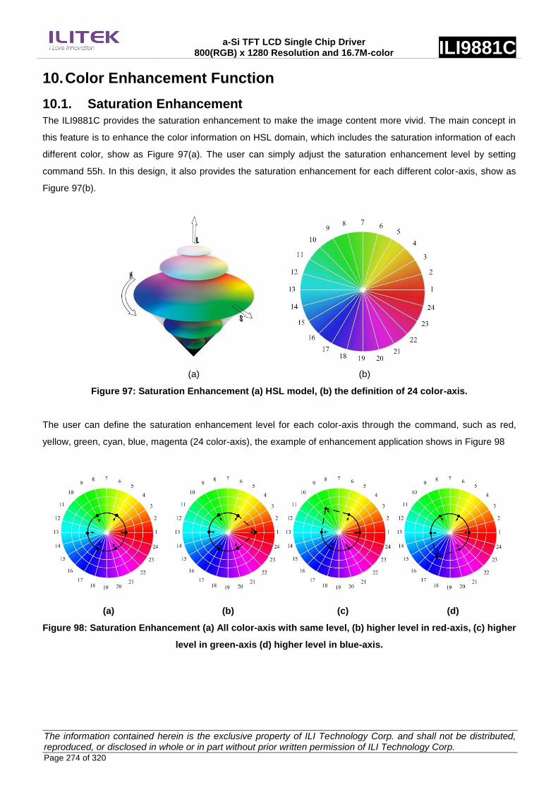
a-Si TFT LCD Single Chip Driver 800(RGB) x 1280 Resolution and 16.7M-color ILI9881C
The information contained herein is the exclusive property of ILI Technology Corp. and shall not be distributed, reproduced, or disclosed in whole or in part without prior written permission of ILI Technology Corp. Page 274 of 320
10. Color Enhancement Function
10.1. Saturation Enhancement The ILI9881C provides the saturation enhancement to make the image content more vivid. The main concept in
this feature is to enhance the color information on HSL domain, which includes the saturation information of each
different color, show as Figure 97(a). The user can simply adjust the saturation enhancement level by setting
command 55h. In this design, it also provides the saturation enhancement for each different color-axis, show as
Figure 97(b).
(a) (b)
Figure 97: Saturation Enhancement (a) HSL model, (b) the definition of 24 color-axis.
The user can define the saturation enhancement level for each color-axis through the command, such as red,
yellow, green, cyan, blue, magenta (24 color-axis), the example of enhancement application shows in Figure 98
(a) (b) (c) (d)
Figure 98: Saturation Enhancement (a) All color-axis with same level, (b) higher level in red-axis, (c) higher
level in green-axis (d) higher level in blue-axis.

a-Si TFT LCD Single Chip Driver 800(RGB) x 1280 Resolution and 16.7M-color ILI9881C
The information contained herein is the exclusive property of ILI Technology Corp. and shall not be distributed, reproduced, or disclosed in whole or in part without prior written permission of ILI Technology Corp. Page 275 of 320
In Figure 99, there is an example for saturation enhancement. Different enhancement levels being applied in this
example.
(a) (b) (c) (d)
Figure 99: Saturation Enhancement Image (a) Original, (b) Low Level, (c) Medium Level, (d) High Level.

a-Si TFT LCD Single Chip Driver 800(RGB) x 1280 Resolution and 16.7M-color ILI9881C
The information contained herein is the exclusive property of ILI Technology Corp. and shall not be distributed, reproduced, or disclosed in whole or in part without prior written permission of ILI Technology Corp. Page 276 of 320
10.2. Contrast Enhancement The contrast between the dark and light, indicate the clarity of the image content. In this design, it provides contrast
enhancement to increase the difference between dark and light to achieve the high contrast image. The user can
select the enhancement level by setting command, the example shows below.
(a) (b)
Figure 100: Contrast Enhancement Image (a) Original, (b) After enhancement

a-Si TFT LCD Single Chip Driver 800(RGB) x 1280 Resolution and 16.7M-color ILI9881C
The information contained herein is the exclusive property of ILI Technology Corp. and shall not be distributed, reproduced, or disclosed in whole or in part without prior written permission of ILI Technology Corp. Page 277 of 320
10.3. Sharpness Enhancement Sharpness enhancement is provided to enhance the image visibility. Unlike contrast enhancement, sharpness
enhancement is to strengthen the object‟s edge to make the object more clearly. The user can select the
enhancement level by setting command, the example shows below.
(a) (b)
Figure 101: Sharpness Enhancement Image (a) Original, (b) After enhancement
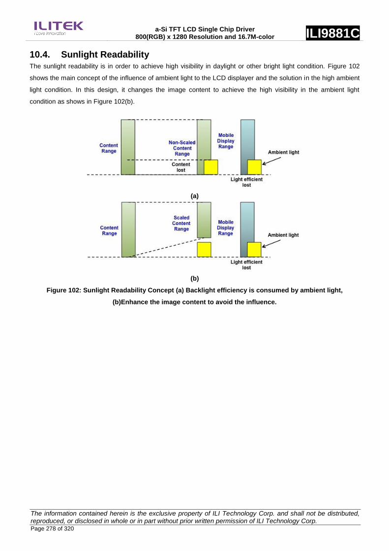
a-Si TFT LCD Single Chip Driver 800(RGB) x 1280 Resolution and 16.7M-color ILI9881C
The information contained herein is the exclusive property of ILI Technology Corp. and shall not be distributed, reproduced, or disclosed in whole or in part without prior written permission of ILI Technology Corp. Page 278 of 320
10.4. Sunlight Readability The sunlight readability is in order to achieve high visibility in daylight or other bright light condition. Figure 102
shows the main concept of the influence of ambient light to the LCD displayer and the solution in the high ambient
light condition. In this design, it changes the image content to achieve the high visibility in the ambient light
condition as shows in Figure 102(b).
(a)
(b)
Figure 102: Sunlight Readability Concept (a) Backlight efficiency is consumed by ambient light,
(b)Enhance the image content to avoid the influence.

a-Si TFT LCD Single Chip Driver 800(RGB) x 1280 Resolution and 16.7M-color ILI9881C
The information contained herein is the exclusive property of ILI Technology Corp. and shall not be distributed, reproduced, or disclosed in whole or in part without prior written permission of ILI Technology Corp. Page 279 of 320
11. Sleep Out Command and Self-Diagnostic Functions
11.1. Register Loading Detection Sleep Out command (See Sleep Out (11h)) is a trigger for an internal function of the display module, which
indicates, if the display module loading function of factory default values from EEPROM (or similar device) to
registers of the display controller works properly.
The display controller will compare factory values of the EEPROM and register values of the display controller (1st
step: compare register and EEPROM values; 2nd
step: load EEPROM value to the register). If those two values
(EEPROM and register values) are the same, a bit is inverted (= increased by 1), which is defined in command
Read Display Self-Diagnostic Result (0Fh) (= RDDSDR) (The used bit of this command is D7). If those values are
not the same, this bit (D7) is not inverted (= not increased by 1). The flow chart for this internal function is as
follows:
Power on sequence
HW reset
SW reset
RDDSDR(0Fh)'s D7 = '0'Sleep IN
mode
Sleep OUT
mode
Sleep IN (10h)
Sleep OUT (11h)
Are EEPROM and
register values same?
D7 inverted
Compares EEPROM and
register values (Note 1)
YE
S
NO
Loads Values from
EEPROM to Registers
Figure 103: Register Loading Detection
Notes: If the EEPROM and loaded register values are not compared, then they can be changed by 00h to AFh and
DAh to DDh commands.

a-Si TFT LCD Single Chip Driver 800(RGB) x 1280 Resolution and 16.7M-color ILI9881C
The information contained herein is the exclusive property of ILI Technology Corp. and shall not be distributed, reproduced, or disclosed in whole or in part without prior written permission of ILI Technology Corp. Page 280 of 320
11.2. Functionality Detection The Sleep Out command (See Sleep Out (11h)) is a trigger for an internal function of the display module. It
indicates if the display module is still running and meets functionality requirements. The internal function (the
display controller) is compared to check if the display module still meets functionality requirements (e.g. booster
voltage levels, timings, etc.). If functionality requirements are met, a bit is inverted (= increased by 1), defined in the
command Read Display Self-Diagnostic Result (0Fh) (RDDSDR) (The used bit of this command is D6). If
functionality requirement is not the same, this bit (D6) is not inverted (= not increased by 1). The flow chart for this
internal function is as follows:
Power on sequence
HW reset
SW reset
RDDSDR(0Fh)'s D6 = '0'Sleep IN
mode
Sleep OUT
mode
Sleep IN (10h)
Sleep OUT (11h)
Check timings, valtage levels,
and other functionalities
Is the required
functionality present?
D6 inverted
YE
S NO
Figure 104: Functionality Detection
Notes: When changing from the Sleep In mode to Sleep Out mode, 120msec are needed after the Sleep Out
command before it is able to check if functionality requirements are met and a value of RDDSDR’s D6 is valid.
Otherwise, there will be 5msec delay for the D6’s value to be valid when the Sleep Out command is sent in the
Sleep Out mode.

a-Si TFT LCD Single Chip Driver 800(RGB) x 1280 Resolution and 16.7M-color ILI9881C
The information contained herein is the exclusive property of ILI Technology Corp. and shall not be distributed, reproduced, or disclosed in whole or in part without prior written permission of ILI Technology Corp. Page 281 of 320
12. Power on/off Sequence
12.1. Power on/off sequence
12.1.1. Power Mode 2A
Input > 0
> 1ms
TVDDI_RISE
TVSP_RISE > 0
> 1us TVSN_FALL
TRES_PULSE
TFS_CMD
>= 0
+/- > 0
VDDITPS_RES
VSP
VSN
RESX
MIPI LanesLP-11 Status MIPI Active
Symbol Characteristics Min. Typ. Max. Units
TVDDI_RISE VDDI Rise time 200 - - us
TVSP_RISE VSP Rise time 200 - - us
TVSN_FALL VSN Fall time 200 - - us
TPS_RES VDDI/VSP on to Reset high 5 - - ms
TRES_PULSE Reset low pulse time 10 - - us
TFS_CMD Reset to first command 10 - - ms
Figure 105: Power on/off sequence with Power Mode 2A

a-Si TFT LCD Single Chip Driver 800(RGB) x 1280 Resolution and 16.7M-color ILI9881C
The information contained herein is the exclusive property of ILI Technology Corp. and shall not be distributed, reproduced, or disclosed in whole or in part without prior written permission of ILI Technology Corp. Page 282 of 320
12.1.2. Power Mode 3
Input > 0
> 1ms
TVDDI_RISE
TVCI_RISE > 1us
TRES_PULSE
TFS_CMD
MIPI LanesLP-11 State MIPI Active
+/- > 0
VDDITPS_RES
VCI
RESX
Symbol Characteristics Min. Typ. Max. Units
TVDDI_RISE VDDI Rise time 200 - - us
TVCI_RISE VCI Rise time 200 - - us
TPS_RES VDDI/VCI on to Reset high 5 - - ms
TRES_PULSE Reset low pulse time 10 - - us
TFS_CMD Reset to first command 10 - - ms
Figure 106: Power on/off sequence with Power Mode 3
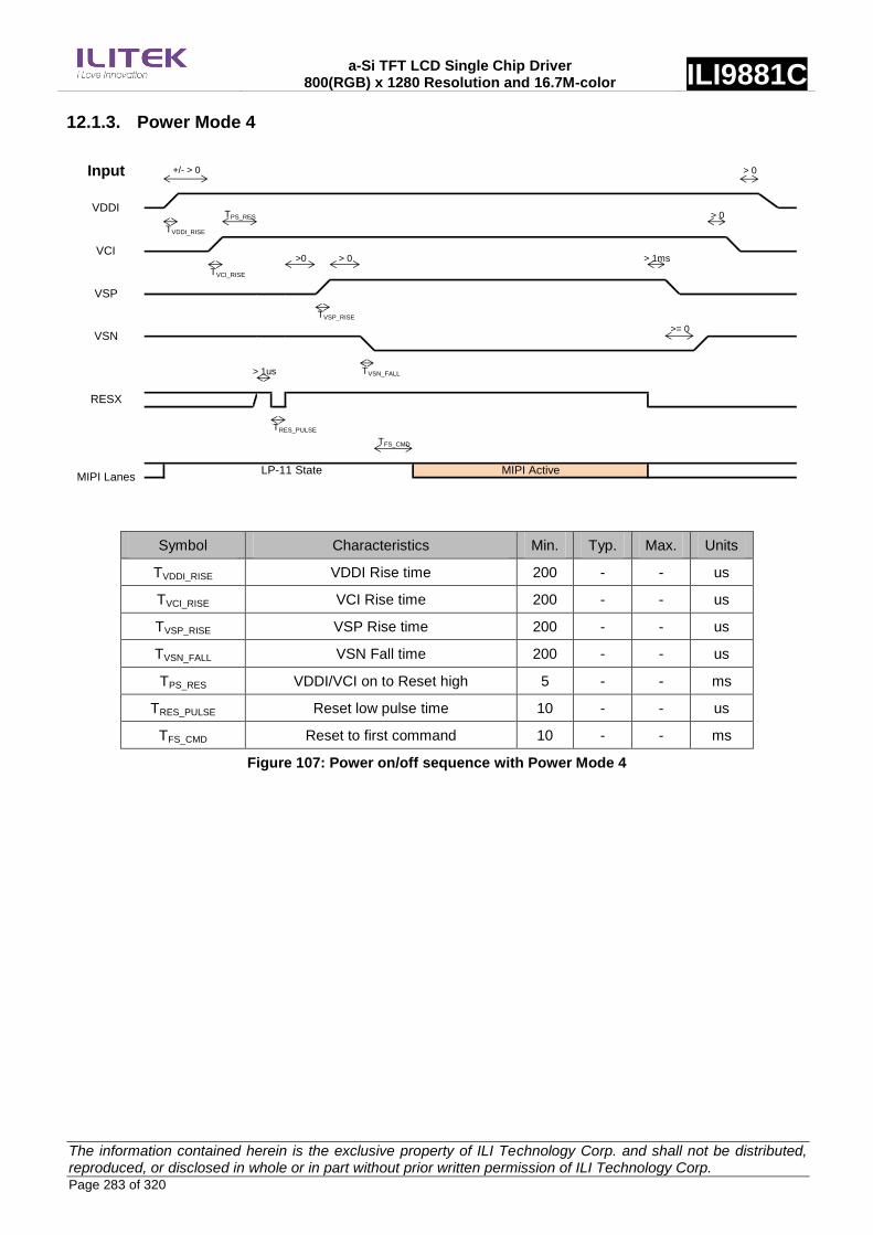
a-Si TFT LCD Single Chip Driver 800(RGB) x 1280 Resolution and 16.7M-color ILI9881C
The information contained herein is the exclusive property of ILI Technology Corp. and shall not be distributed, reproduced, or disclosed in whole or in part without prior written permission of ILI Technology Corp. Page 283 of 320
12.1.3. Power Mode 4
Input > 0
> 0
TVDDI_RISE
>0 > 0 > 1ms
TVCI_RISE
TVSP_RISE
> 1us TVSN_FALL
TRES_PULSE
TFS_CMD
+/- > 0
VDDITPS_RES
VCI
VSP
>= 0
RESX
MIPI LanesLP-11 State MIPI Active
VSN
Symbol Characteristics Min. Typ. Max. Units
TVDDI_RISE VDDI Rise time 200 - - us
TVCI_RISE VCI Rise time 200 - - us
TVSP_RISE VSP Rise time 200 - - us
TVSN_FALL VSN Fall time 200 - - us
TPS_RES VDDI/VCI on to Reset high 5 - - ms
TRES_PULSE Reset low pulse time 10 - - us
TFS_CMD Reset to first command 10 - - ms
Figure 107: Power on/off sequence with Power Mode 4
a-Si TFT LCD Single Chip Driver 800(RGB) x 1280 Resolution and 16.7M-color ILI9881C
The information contained herein is the exclusive property of ILI Technology Corp. and shall not be distributed, reproduced, or disclosed in whole or in part without prior written permission of ILI Technology Corp. Page 284 of 320
12.2. Uncontrolled Power Off The uncontrolled power off means a situation when a battery is removed without the controlled power off sequence.
There will not be any damages for the display module, or the display module will not cause any damages for the
host or lines of the interface. At an uncontrolled power off event, the ILI9881C will force the display to become
blank and will not have any abnormal visible effects within 1 second on the display and remains blank until the
Power On Sequence powers it up.

a-Si TFT LCD Single Chip Driver 800(RGB) x 1280 Resolution and 16.7M-color ILI9881C
The information contained herein is the exclusive property of ILI Technology Corp. and shall not be distributed, reproduced, or disclosed in whole or in part without prior written permission of ILI Technology Corp. Page 285 of 320
13. Power Level Definition
13.1. Power Levels 4 level modes are defined in order from Maximum to Minimum Power consumption:
1. Normal Mode On (full display), Sleep Out, Idle Mode Off.
In this mode, the display is able to show a maximum of 16.7M colors.
2. Normal Mode On (full display), Sleep Out, Idle Mode On.
In this mode, the display is able to show a maximum of 2 colors.
3. Sleep In Mode.
In this mode, the DC/DC converter, internal oscillator and panel driver circuit are stopped.
4. Power Off Mode.
In this mode, all input powers are removed.
Transition between modes 1-3 is controllable by MCU commands. Mode 4 is entered only when both Power
supplies are removed.
13.2. Power Flow Chart
Power ON sequence
HW reset
SW reset
Sleep IN
Normal display mode ON
Idle mode OFF
Sleep OUT
Normal display mode ON
Idle mode OFF
SLPIN
SLPOUT
Normal display mode ON = NORON
Idle mode OFF = IDMOFF
Idle mode ON = IDMON
Sleep OUT = SLPOUT
Sleep IN = SLPIN
Sleep OUT
Normal display mode ON
Idle mode ON
IDMOFFIDMON
Figure 1085: Power Mode Flow Chart
Notes:
1. There is not any abnormal visual effect when one power mode changes to another power mode.
2. There is not any limitation, which is not specified by User, when one power mode changes to another power
mode.

a-Si TFT LCD Single Chip Driver 800(RGB) x 1280 Resolution and 16.7M-color ILI9881C
The information contained herein is the exclusive property of ILI Technology Corp. and shall not be distributed, reproduced, or disclosed in whole or in part without prior written permission of ILI Technology Corp. Page 286 of 320
14. Characteristics of I/O
14.1. Output or Bi-directional (I/O) Pins
Table 34: Characteristics of Output or Bi-directional (I/O) Pins
Pin/Line After
Power ON
After
Hardware Reset
After
Software Reset
D0P Hi-Z (Inactive) Hi-Z (Inactive) Hi-Z (Inactive)
D0N Hi-Z (Inactive) Hi-Z (Inactive) Hi-Z (Inactive)
VS Hi-Z (Inactive) Hi-Z (Inactive) Hi-Z (Inactive)
HS Hi-Z (Inactive) Hi-Z (Inactive) Hi-Z (Inactive)
LEDPWM Low Low Low
TE Low Low Low
Note: There will be no output from D0P, D0N, VS, HS, LEDPWM and TE during Power ON/OFF sequence,
hardware reset, and software reset.
14.2. Input Pins
Table 35: Input Pins
Pin/Line
During
Power ON
Process
After
Power ON
After Hardware
Reset
After
Software
Reset
During
Power OFF
Process
RESX See
chapter 12 Input valid Input valid Input valid
See
chapter 12
IM[2:0] Input invalid Input valid Input valid Input valid Input invalid
LANSEL Input invalid Input valid Input valid Input valid Input invalid
RS[1:0] Input invalid Input valid Input valid Input valid Input invalid
BOOSTM[2:0] Input invalid Input valid Input valid Input valid Input invalid
CLKP Input invalid Input valid Input valid Input valid Input invalid
CLKN Input invalid Input valid Input valid Input valid Input invalid
D0P Input invalid Input valid Input valid Input valid Input invalid
D0N Input invalid Input valid Input valid Input valid Input invalid
D1P Input invalid Input valid Input valid Input valid Input invalid
D1N Input invalid Input valid Input valid Input valid Input invalid
D2P Input invalid Input valid Input valid Input valid Input invalid
D2N Input invalid Input valid Input valid Input valid Input invalid
D3P Input invalid Input valid Input valid Input valid Input invalid
D3N Input invalid Input valid Input valid Input valid Input invalid

a-Si TFT LCD Single Chip Driver 800(RGB) x 1280 Resolution and 16.7M-color ILI9881C
The information contained herein is the exclusive property of ILI Technology Corp. and shall not be distributed, reproduced, or disclosed in whole or in part without prior written permission of ILI Technology Corp. Page 287 of 320
15. NV Memory Programming Flow
15.1. External MTP_PWR Programming Flow
No
Start
Reset
Supply External
8.5V to MTP_PWR pin
Wait 10ms
Wait 10ms
Cut Off External
8.5V Power
Reset
End
Yes
NV Memory Protection Key
Register E3h : 55h
Register E4h : AAh
Register E5h : 66h
NV Memory Write
Register E0h : PGM_DATA[7:0]=xxh (xx=8 bit OTP value)
Register E1h : PGM_ADR[7:0]=8 b́xxxxxxxx
Register E2h : PGM_ADR[15:8]=8 b́xxxxxxxx
Check E6h~E8h
(ID1,2,3)_Mk= 3 b́111?
(VCM1, 2)_Mk= 3 b́111?
(GAMMAP,N)_Mk = 1'b1?
Wait 120ms
Register
Address
FFh
1st parameter
Device code 1
98h
2nd parameter
Device code 2
81h
3rd parameter
Page_select
01h
Entry the Page1
Sleep Out Mode
Display OFF
Operation
After Reset the Driver IC enter
sleep in mode
Sleep Out
(Page 0 / R11h)
Wait 10ms
Figure 109: External MTP_PWR Programming Flow
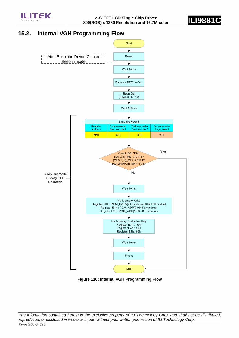
a-Si TFT LCD Single Chip Driver 800(RGB) x 1280 Resolution and 16.7M-color ILI9881C
The information contained herein is the exclusive property of ILI Technology Corp. and shall not be distributed, reproduced, or disclosed in whole or in part without prior written permission of ILI Technology Corp. Page 288 of 320
15.2. Internal VGH Programming Flow
No
Start
Reset
Wait 10ms
Wait 10ms
Page 4 / RD7h = 04h
Reset
End
Yes
NV Memory Protection Key
Register E3h : 55h
Register E4h : AAh
Register E5h : 66h
NV Memory Write
Register E0h : PGM_DATA[7:0]=xxh (xx=8 bit OTP value)
Register E1h : PGM_ADR[7:0]=8 b́xxxxxxxx
Register E2h : PGM_ADR[15:8]=8 b́xxxxxxxx
Check E6h~E8h
(ID1,2,3)_Mk= 3 b́111?
(VCM1, 2)_Mk= 3 b́111?
(GAMMAP,N)_Mk = 1'b1?
Wait 120ms
Register
Address
FFh
1st parameter
Device code 1
98h
2nd parameter
Device code 2
81h
3rd parameter
Page_select
01h
Entry the Page1
Sleep Out Mode
Display OFF
Operation
After Reset the Driver IC enter
sleep in mode
Sleep Out
(Page 0 / R11h)
Wait 10ms
Figure 110: Internal VGH Programming Flow

a-Si TFT LCD Single Chip Driver 800(RGB) x 1280 Resolution and 16.7M-color ILI9881C
The information contained herein is the exclusive property of ILI Technology Corp. and shall not be distributed, reproduced, or disclosed in whole or in part without prior written permission of ILI Technology Corp. Page 289 of 320
16. Gamma Correction
VREG1OUT
(VREG2OUT)
P0
P1
P2
6bit DAC P[126:0:2]
7bit DAC P[254:0:2]
7bit DAC P[254:0:2]
X0
X1
X174
6bit DAC
X[78:15]
7bit DAC
X[151:24]
6bit DAC
X[131:68]
X1758bit DAC P[383:128]
0
4
8
80
Y0
Y1
Y110
6bit DAC
Y[75:12]
6bit DAC
Y[100:37]
Y1128bit DAC P[512:257]
175
Z0
Z1
Z174
7bit DAC
Z[151:24]
6bit DAC
Z[160:97]
6bit DAC
Z[174:111]
Z1757bit DAC P[640:386:2]
247
7bit DAC P[640:386:2]
6bit DAC P[640:514:2]
251
255
P127
P128
P255
P256
P383
P384
P638
P639
P640
16
24
36
111
144
231
239
243
VGSP
(VGSN)
640R
175R
112R
175R
4R
4R
4R
8R
12R
16R
31R
33R
31R
28R
8R
4R
4R
4R
4R
6bit DAC
X[64:1]12
4R
GMA0
GMA4
GMA8
GMA12
GMA16
GMA24
GMA36
GMA52
GMA80
GMA111
GMA144
GMA175
GMA203
GMA219
GMA231
GMA243
GMA239
GMA251
6bit DAC
X[163:100]52
28R
6bit DAC
Z[75:12]203
6bit DAC
Z[107:44]219
16R
12R
GMA247
GMA255
GMA[3:1]
GMA[7:5]
GMA[11:9]
GMA[15:13]
GMA[254:252]
GMA[250:248]
GMA[246:244]
GMA[242:240]
GMA[238:232]
GMA[230:220]
GMA[218:204]
GMA[202:176]
GMA[174:145]
GMA[143:112]
GMA[110:81]
GMA[79:53]
GMA[51:37]
GMA[35:25]
GMA[23:17]
Figure 111: Gamma Architecture

a-Si TFT LCD Single Chip Driver 800(RGB) x 1280 Resolution and 16.7M-color ILI9881C
The information contained herein is the exclusive property of ILI Technology Corp. and shall not be distributed, reproduced, or disclosed in whole or in part without prior written permission of ILI Technology Corp. Page 290 of 320
17. Touch Synchronization Signal
The VS and HS pad of ILI9881C can output the synchronization signals to touch sensing signal for touch panel
controller. To use these signals, touch panel controller can receive touch sensing signal while avoiding display
changing noise.
These signals are consist of vertical synchronization signal: VSOUT and horizontal synchronization signal: HSOUT.
The level of output voltage is IOVCC to GND. Each signal can adjust output timing for internal synchronization
signal. The high level width of VSOUT is 1 line, and it is adjustable. VSOUT is outputted always, but HSOUT is
outputted during displaying only.
(1) VSOUT output Timing
VSOUT output means internal VSYNC is starting point. VSOUT output timing can be adjusted by VSOD register.
Unit is 1H.
(2) HSOUT output Timing
HSOUT output means internal source output timing is starting point. HSOUT output timing can be adjusted by
HSOD register. And HSOUT high level width can be adjusted by HSOHW register.
Internal V-Sync
Internal H-Sync
1H
1H
1 Frame
VOSD=2'b00
VSOUT
HSOUT
FP
Period
BP
Period
FP
Period
BP
Period
Display Off
1 Frame
1H
HSOHW
HSOD
HSOD
Display On
HSOHW
Figure 112: Touch Synchronization Signal

a-Si TFT LCD Single Chip Driver 800(RGB) x 1280 Resolution and 16.7M-color ILI9881C
The information contained herein is the exclusive property of ILI Technology Corp. and shall not be distributed, reproduced, or disclosed in whole or in part without prior written permission of ILI Technology Corp. Page 291 of 320
18. Electrical Characteristics
18.1. Absolute Maximum Ratings (TBD) The absolute maximum rating is listed in Table 36. When the ILI9881C is used out of the absolute maximum
ratings, it may be permanently damaged. To use the ILI9881C within the following electrical characteristics limit is
strongly recommended for normal operation. If these electrical characteristic conditions are exceeded during
normal operation, the ILI9881C will malfunction and cause poor reliability.
Table 36: Absolute Maximum Ratings
Item Symbol Unit Value
Analog Operating Voltage VCI ~ GND V -0.3 ~ +6.5
Analog Operating Voltage VCIREF ~ GND V -0.3 ~ +6.5
Digital Operating Voltage VDDI ~ GND V -0.3 ~ +3.3
Digital Operating Voltage VCC1 ~ GND V -0.3 ~ +3.3
Digital Operating Voltage VCC2 ~ GND V -0.3 ~ +3.3
DSI Operating Voltage VDDAM ~ GND V -0.3 ~ +3.3
OTP Supply Voltage MTP_PWR ~ GND V -0.3 ~ +9.0
Supply Voltage VSP ~ GND V -0.3 ~ +6.5
Supply Voltage VSN ~ GND V 0.3 ~ -6.5
Gate Driver High Voltage VGH ~ GND V -0.3 ~ +18
Gate Driver Low Voltage VGL ~ GND V 0.3 ~ -18
Driver Supply Voltage VCI - VCL V ≦ 6.0V
Driver Supply Voltage VGH - VGL V ≦ 32.0V
Input Voltage VIN V -0.3 ~ VDDI + 0.3
HS Input Voltage VHSIN V -0.3 ~ + 1.65
Operating Temperature Topr ℃ -30 ~ +70
Storage Temperature Tstg ℃ -55 ~ +110
Note: Even if the absolute maximum rating of one of the above parameters is exceeded only for a short while,
the quality of the product may be degraded. Therefore, be sure to use the product within the range of the
absolute maximum ratings.

a-Si TFT LCD Single Chip Driver 800(RGB) x 1280 Resolution and 16.7M-color ILI9881C
The information contained herein is the exclusive property of ILI Technology Corp. and shall not be distributed, reproduced, or disclosed in whole or in part without prior written permission of ILI Technology Corp. Page 292 of 320
18.2. DC Characteristics for Panel Driving Item Symbol Condition Min. Typ. Max. Unit Note
Power & Operation Voltage
Analog operating voltage VCI - 2.5 2.8 6.0 V
Analog operating voltage VCIREF 2.5 2.8 6.0
Digital operating voltage VDDI - 1.65 2.8 3.3 V
Digital operating voltage VCC1 1.75 2.8 6.0 V
Digital operating voltage VCC2 1.75 2.8 6.0 V
DSI operating voltage VDDAM - 1.75 1.8 3.3 V
OTP Supply voltage MTP_PWR - - 8.5 - V
Analog operating voltage VSP - 4.5 6 V
Analog operating voltage VSN - -6 -4.5 V
Logic High level input voltage VIH - 0.7*VDDI VDDI V Note1
Logic Low level input voltage VIL - -0.3 0.3*VDDI V Note1
Logic High level output voltage
TE , LEDPWM VOH IOH = -1.0mA 0.8*VDDI VDDI V Note1
Logic Low level output voltage
TE , LEDPWM VOL IOL = +1.0mA 0 0.2*VDDI V Note1
Gate Driver High Voltage VGH - 8.0 - 18 V
Gate Driver Low Voltage VGL - -18.0 - -7.0 V
Driver Supply Voltage - |VGH-VGL| 15 - 32 V
VCOM Operation
DC VCOM Amplitude Voltage VCOM - -4.0 - 0 V Note3
Source Driver
Source Output Range VSOUT - 0.5 - VREG1OUT-0.5 V Note4
Positive Gamma Reference Voltage VREG1OUT - 2.9 - 5.5 V
Negative Gamma Reference Voltage VREG2OUT - -5.5 - -2.9 V
Source Output Setting Time Tr Below with 99%
precision -
10
(TBD) - uS Note3.4
Output Deviation Voltage
(Source Output channel) Vdev
Sout>=4.2V
Sout<=0.8V - - 20 (TBD) mV Note3
4.2V>Sout>0.8V - - 15 (TBD) mV
Output Offset Voltage VOFFSET - - - 35 (TBD) mV Note3
Standby mode current consumption
Sleep In mode
I(VDDI SLP
IN) Ta = 25 °C
VCI=2.8V
VDDI=1.8V
- (TBD) (TBD) uA
I(VCI SLP IN) - (TBD) (TBD) uA
Notes:
1. Ta = -30 to 70 °C (to 85 °C no damage) , VCI = 2.5V to 6.0V, VDDI = 1.65V to 3.3V
2. Supply digital VDDI voltage equal or less than analog VCI voltage.
3. Source channel loading = (TBD)
4. The maximum value is between with (TBD) and Gamma setting value

a-Si TFT LCD Single Chip Driver 800(RGB) x 1280 Resolution and 16.7M-color ILI9881C
The information contained herein is the exclusive property of ILI Technology Corp. and shall not be distributed, reproduced, or disclosed in whole or in part without prior written permission of ILI Technology Corp. Page 293 of 320
18.3. DSI DC Characteristics The DSI uses different state codes which depend on DC voltage levels of the clock and data lanes. The meaning of
the state codes is defined in the following table.
State Code Line DC Voltage Levels
CLOCK_P or DATA_P CLOCK_N or DATA_N
HS-0 Low (HS) High (HS)
HS-1 High (HS) Low (HS)
LP-00 Low (LP) Low (LP)
LP-01 Low (LP) High (LP)
LP-10 High (LP) Low (LP)
LP-11 High (LP) High (LP)
Note: Ta = -30℃ to 70℃ (to +85℃ no damage)
18.3.1. DC Characteristics for Power Lines
Parameter Symbol Condition Specification
Unit Min. Typ. Max.
Analog power supply voltage VCI Operating voltage 2.5 2.8 6.0 V
Digital power supply voltage VDDI Operating voltage 1.65 1.8 3.3 V
Analog power supply voltage
noise VVCI_NOISE
Noise Range, 0 to 100MHz,
Sinusoidal Wave (peak-to-peak) - - 100 mV
Noise Range, 0 to 30kHz,
Pulse Wave with Duty Cycle (50%/50%) - - 500 mV
Digital power supply voltage
noise VVDDI_NOISE
Noise Range, 0 to 100MHz,
Sinusoidal Wave (peak-to-peak) - - 100 mV
Notes:
1. Ta = -30℃ to 70℃ (to +85℃ no damage)
2. These values are not symmetric amplitude, which center points are VDDI or VCI. See examples, when
VVCI_NOISE and VVDDI_NOISE are maximums, as reference purposes below.
VCI
VCI
VDDI
VDDI
GND
Figure 113: Noise on Power Supply Lines

a-Si TFT LCD Single Chip Driver 800(RGB) x 1280 Resolution and 16.7M-color ILI9881C
The information contained herein is the exclusive property of ILI Technology Corp. and shall not be distributed, reproduced, or disclosed in whole or in part without prior written permission of ILI Technology Corp. Page 294 of 320
18.3.2. DC Characteristics for DSI LP Mode
DC levels of the LP-00, LP-01, LP-10 and LP-11 are defined in the table below: DC Characteristics for the DSI LP
mode when LP-RX, LP-CD or LP-TX is mentioned in the condition column. Other logical levels in the table are for
MCU interface.
Parameter Symbol Condition Specification Unit
Min. Typ. Max.
Logic 1 input voltage VIHLPCD LP-CD 450 - 1350 mV
Logic 0 input voltage VILLPCD LP-CD 0.0 - 200 mV
Logic 1 input voltage VIHLPRX LP-RX (CLK, D0 ,D1, D2, D3) 880 - 1350 mV
Logic 0 input voltage VILLPRX LP-RX (CLK, D0 ,D1, D2, D3) 0.0 - 550 mV
Logic 0 input voltage VILLPRXULP LP-RX (CLK ULP mode) 0.0 - 300 mV
Logic 1 output voltage VOHLPTX LP-TX (D0) 1.1 - 1.3 V
Logic 0 output voltage VOLLPTX LP-TX (D0) -50 - 50 mV
Logic 1 input current IIH LP-CD, LP-RX - - 10 uA
Logic 0 input current IIL LP-CD, LP-RX -10 - - uA
Notes:
1.Ta = -30℃ to 70℃ (to +85℃ no damage)
2. DSI High Speed mode is off.
18.3.3. Spike/Glitch Rejection
Figure 114: Spike/Glitch Rejection
Notes:
1. A spike/glitch can be rejected when the Peak Interference Amplitude is 200mV (at maximum) and Interference
Frequency is 450MHz (at the very least).
2. n = 0 and 1.
Table 37: Spike/Glitch Rejection
Spike/Glitch Rejection – DSI
Signal Symbol Parameter Min Max Unit
CLKP/N, DnP/N SGD Input pulse rejection for DSI - 300 Vps

a-Si TFT LCD Single Chip Driver 800(RGB) x 1280 Resolution and 16.7M-color ILI9881C
The information contained herein is the exclusive property of ILI Technology Corp. and shall not be distributed, reproduced, or disclosed in whole or in part without prior written permission of ILI Technology Corp. Page 295 of 320
18.3.4. DC Characteristics for DSI HS mode
Parameter Symbol Condition Specification Unit
Input Common Mode Voltage for Clock VCMCLK CLKP/N
Note 2, Note 3 70 - 330 mV
Input Common Mode Voltage for Data VCMDATA DnP/N
Note 2, Note 3, Note 5 70 - 330 mV
Common Mode Ripple for Clock Equal or Less
than 450MHz VCMRCLKL450
CLKP/N
Note 4 -50 - 50 mV
Common Mode Ripple for Data Equal or Less
than 450MHz VCMRDATAL450
DnP/N
Note 4, Note 5 -50 - 50 mV
Common Mode Ripple for Clock More than
450MHz (peak sine wave) VCMRCLKM450 CLKP/N - - 100 mV
Common Mode Ripple for Data More than
450MHz (peak sine wave) VCMRDATAM450
DnP/N
Note 5 - - 100 mV
Differential Input Low Level Threshold Voltage
for Clock VTHLCLK- CLKP/N -70 - - mV
Differential Input Low Level Threshold Voltage
for Data VTHLDATA-
DnP/N
Note 5 -70 - - mV
Differential Input High Level Threshold Voltage
for Clock VTHHCLK+ CLKP/N - - 70 mV
Differential Input High Level Threshold Voltage
for Data VTHHDATA+
DnP/N
Note 5 - - 70 mV
Single-ended Input Low Voltage VILHS CLKP/N, DnP/N
Note 3, Note 5 -40 - - mV
Single-ended Input High Voltage VIHHS CLKP/N, DnP/N
Note 3, Note 5 - - 460 mV
Differential Termination Resistor RTERM CLKP/N, DnP/N
Note 5 80 100 125 Ω
Single-ended Threshold Voltage for
Termination Enable VTERM-EN
CLKP/N, DnP/N
Note 5 - - 450 mV
Termination Capacitor CTERM CLKP/N, DnP/N
Note 5, Note 6 - - 60 pF
Notes:
1. Ta = -30℃ to 70℃ (to +85℃ no damage) , VCI = 2.5V to 6.0V, VDDI = 1.65V to 3.3V
2. Includes 50mV (-50mV to 50mV) ground difference
3. Without VCMRCLKM450/VCMRDATAM450
4. Without 50mV (-50mV to 50mV) ground difference
5. n = 0 and 1
6. For higher bit rates, a 14pF capacitor will be needed to meet the common-mode return loss specification.

a-Si TFT LCD Single Chip Driver 800(RGB) x 1280 Resolution and 16.7M-color ILI9881C
The information contained herein is the exclusive property of ILI Technology Corp. and shall not be distributed, reproduced, or disclosed in whole or in part without prior written permission of ILI Technology Corp. Page 296 of 320
The DSI receiver (HS mode) understands that there is logical 1 (= HS-1) when a differential voltage is more than
VTHH (CLKP/DnP). The DSI receiver (HS mode) understands that there is logical 0 (= HS-0) when a differential
voltage is more than VTHL (CLKN/DnN). There is undefined state if the differential voltage is less than VTHH
(CLKP/DnP) and less than VTHL (CLKN/DnN). A reference figure is below.
Figure 115: Differential Inputs Logical 0 and 1, Threshold High/Low, Differential Voltage Range
Note: n = 0, 1, 2 and 3
Figure 116: Common Mode Voltage on Clock and Data Channels
CLKP/N,
DnP/N
CLKP
CLKN
DnP
DnN
n = 0, 1, 2 and 3

a-Si TFT LCD Single Chip Driver 800(RGB) x 1280 Resolution and 16.7M-color ILI9881C
The information contained herein is the exclusive property of ILI Technology Corp. and shall not be distributed, reproduced, or disclosed in whole or in part without prior written permission of ILI Technology Corp. Page 297 of 320
The termination resistor (RTERM) of the differential DSI receiver can be driven to two different states by the
receiver:
Low Power (LP) mode when the termination resistor is not connected between differential inputs (CLKP
<=> CLKN or D0P <=> D0N or D1P <=> D2N or D2P <=> D3N or D1P <=> D3N)
High Speed (HS) mode when the termination resistor is connected between differential inputs (CLKP
<=> CLKN or D0P <=> D0N or D1P <=> D2N or D2P <=> D3N or D1P <=> D3N)
The termination switch (HS/LP), when the termination resistor is not connected, is illustrated below.
Figure 117: Differential Pair Termination Resistor on the Receiver Side
CLKP,
DnP
CLKN,
DnN
n = 0, 1, 2 and 3

a-Si TFT LCD Single Chip Driver 800(RGB) x 1280 Resolution and 16.7M-color ILI9881C
The information contained herein is the exclusive property of ILI Technology Corp. and shall not be distributed, reproduced, or disclosed in whole or in part without prior written permission of ILI Technology Corp. Page 298 of 320
18.4. AC Characteristics
18.4.1. DSI Timing Characteristics
18.4.2. High Speed Mode – Clock Channel Timing
Figure 118: DSI Clock Channel Timing
Table 38: DSI Clock Channel Timing
Signal Symbol Parameter Min Max Unit
CLKP/N 2xUIINST Double UI instantaneous 4 25 ns
CLKP/N UIINSTA,UIINSTB
(Note 1) UI instantaneous Half
2
(Note 2) 12.5 ns
Notes:
1. UI = UIINSTA = UIINSTB
2. Define the minimum value of 24 UI per Pixel, see Table 39.
Table 39: Limited Clock Channel Speed
Data type Two Lanes
speed
Three Lanes
speed
Four Lanes
speed
Data Type = 00 1110 (0Eh), RGB 565, 16 UI per Pixel 566 Mbps 433 Mbps 366 Mbps
Data Type = 01 1110 (1Eh), RGB 666, 18 UI per Pixel 637 Mbps 487 Mbps 412 Mbps
Data Type = 10 1110 (2Eh), RGB 666 Loosely, 24 UI per Pixel 850 Mbps 650 Mbps 550 Mbps
Data Type = 11 1110 (3Eh), RGB 888, 24 UI per Pixel 850 Mbps 650 Mbps 550 Mbps
CLKP
CLKN CLKP
CLKN

a-Si TFT LCD Single Chip Driver 800(RGB) x 1280 Resolution and 16.7M-color ILI9881C
The information contained herein is the exclusive property of ILI Technology Corp. and shall not be distributed, reproduced, or disclosed in whole or in part without prior written permission of ILI Technology Corp. Page 299 of 320
18.4.3. High Speed Mode – Data Clock Channel Timing
Figure 119: DSI Data to Clock Channel Timings
Table 40: DSI Data to Clock Channel Timings
Signal Symbol Parameter Min Max
DnP/N , n=0 and 1 tDS Data to Clock Setup time 0.15xUI -
tDH Clock to Data Hold Time 0.15xUI -
DnP
DnN
n = 0, 1, 2, 3
CLKP
CLKN
CLKP, DnP
CLKN, DnN

a-Si TFT LCD Single Chip Driver 800(RGB) x 1280 Resolution and 16.7M-color ILI9881C
The information contained herein is the exclusive property of ILI Technology Corp. and shall not be distributed, reproduced, or disclosed in whole or in part without prior written permission of ILI Technology Corp. Page 300 of 320
18.4.4. High Speed Mode – Rising and Falling Timings
Figure 120: Rising and Falling Timings on Clock and Data Channels
Table 41: Rise and Fall Timings on Clock and Data Channels
Parameter Symbol Condition Specification
Min Typ Max
Differential Rise Time for Clock tDRTCLK CLKP/N 150 ps - 0.3UI
(Note)
Differential Rise Time for Data tDRTDATA DnP/N
n=0 and 1 150 ps -
0.3UI
(Note)
Differential Fall Time for Clock tDFTCLK CLKP/N 150 ps - 0.3UI
(Note)
Differential Fall Time for Data tDFTDATA DnP/N
n=0 and 1 150 ps -
0.3UI
(Note)
Note: The display module has to meet timing requirements, which are defined for the transmitter (MCU) on MIPI
D-Phy standard.
CLKP/N
DnP/N
n = 0, 1, 2, 3

a-Si TFT LCD Single Chip Driver 800(RGB) x 1280 Resolution and 16.7M-color ILI9881C
The information contained herein is the exclusive property of ILI Technology Corp. and shall not be distributed, reproduced, or disclosed in whole or in part without prior written permission of ILI Technology Corp. Page 301 of 320
18.4.5. Low Speed Mode – Bus Turn Around
Lower Power Mode and its State Periods on the Bus Turnaround (BTA) from the MCU to the Display Module
(ILI9881C) are illustrated for reference purposes below.
Figure 121: BTA from the MCU to the Display Module
Lower Power Mode and its State Periods on the Bus Turnaround (BTA) from the Display Module (ILI9881C) to the
MCU are illustrated for reference purposes below.
Figure 122: BTA from the Display Module to the MCU
Table 42: Low Power State Period Timings – A
Signal Symbol Description Min Max Unit
D0P/N TLPXM Length of LP-00, LP-01, LP-10 or LP-11 periods
MCU Display Module (ILI9881C) 50 75 ns
D0P/N TLPXD Length of LP-00, LP-01, LP-10 or LP-11 periods
Display Module (ILI9881C) MCU 50 75 ns
D0P/N TTA-SURED Time-out before the Display Module (ILI9881C) starts driving TLPXD 2xTLPXD ns
Table 43: Low Power State Period Timings – B
Signal Symbol Description Time Unit
D0P/N TTA-GETD Time to drive LP-00 by Display Module (ILI9881C) 5xTLPXD ns
D0P/N TTA-GOD Time to drive LP-00 after turnaround request - MCU 4xTLPXD ns
D0P
D0N
D0P
D0N
D0P
D0N
D0P
D0N

a-Si TFT LCD Single Chip Driver 800(RGB) x 1280 Resolution and 16.7M-color ILI9881C
The information contained herein is the exclusive property of ILI Technology Corp. and shall not be distributed, reproduced, or disclosed in whole or in part without prior written permission of ILI Technology Corp. Page 302 of 320
18.4.6. Data Lanes from Low Power Mode to High Speed Mode
Figure 123: Data Lanes - Low Power Mode to High Speed Mode Timings
Table 44: Data Lanes - Low Power Mode to High Speed Mode Timings
Signal Symbol Description Min Max Unit
DnP/N, n = 0 and 1 TLPX Length of any Low Power State Period 50 - ns
DnP/N, n = 0 and 1 THS-PREPARE Time to drive LP-00 to prepare for HS Transmission 40+4xUI 85+6xUI ns
DnP/N, n = 0 and 1 THS-TERM-EN Time to enable Data Lane Receiver line termination
measured from when Dn crosses VILMAX
- 35+4xUI ns
CLKP, DnP
CLKN, DnN
CLKP
CLKN DnP
DnN
n= 0, 1, 2, 3
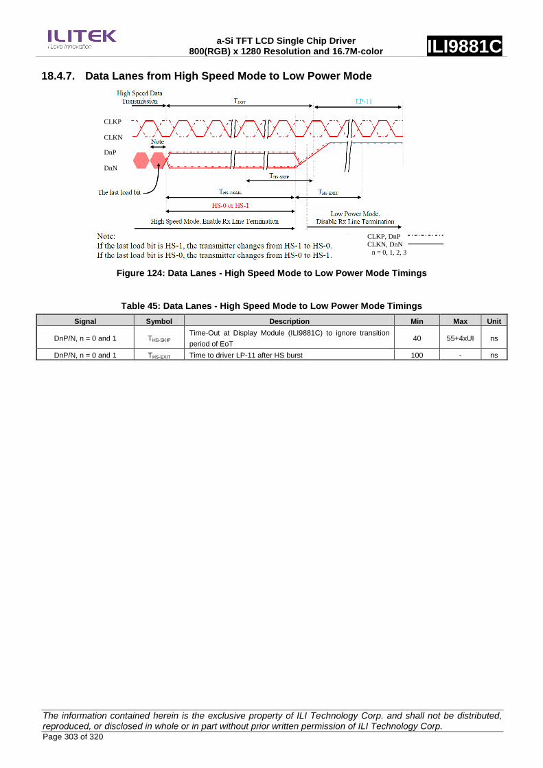
a-Si TFT LCD Single Chip Driver 800(RGB) x 1280 Resolution and 16.7M-color ILI9881C
The information contained herein is the exclusive property of ILI Technology Corp. and shall not be distributed, reproduced, or disclosed in whole or in part without prior written permission of ILI Technology Corp. Page 303 of 320
18.4.7. Data Lanes from High Speed Mode to Low Power Mode
Figure 124: Data Lanes - High Speed Mode to Low Power Mode Timings
Table 45: Data Lanes - High Speed Mode to Low Power Mode Timings
Signal Symbol Description Min Max Unit
DnP/N, n = 0 and 1 THS-SKIP Time-Out at Display Module (ILI9881C) to ignore transition
period of EoT 40 55+4xUI ns
DnP/N, n = 0 and 1 THS-EXIT Time to driver LP-11 after HS burst 100 - ns
CLKP, DnP
CLKN, DnN
n = 0, 1, 2, 3
CLKP
CLKN
DnP
DnN

a-Si TFT LCD Single Chip Driver 800(RGB) x 1280 Resolution and 16.7M-color ILI9881C
The information contained herein is the exclusive property of ILI Technology Corp. and shall not be distributed, reproduced, or disclosed in whole or in part without prior written permission of ILI Technology Corp. Page 304 of 320
18.4.8. DSI Clock Burst – High Speed Mode to/from Low Power Mode
Figure 125: Clock Lanes - High Speed Mode to/from Low Power Mode Timings
Table 46: Clock Lanes - High Speed Mode to/from Low Power Mode Timings
Signal Symbol Description Min Max Unit
CLKP/N TCLK-POST Time that the MCU shall continue sending HS clock after the
last associated Data Lanes has transitioned to LP mode 60+52xUI - ns
CLKP/N TCLK-TRAIL Time to drive HS differential state after last payload clock bit of
a HS transmission burst 60 - ns
CLKP/N THS-EXIT Time to drive LP-11 after HS burst 100 - ns
CLKP/N TCLK-PREPARE Time to drive LP-00 to prepare for HS transmission 38 95 ns
CLKP/N TCLK-TERM-EN Time-out at Clock Lane to enable HS termination - 38 ns
CLKP/N TCLK-PREPARE
+ TCLK-ZERO Minimum lead HS-0 drive period before starting Clock 300 - ns
CLKP/N TCLK-PRE Time that the HS clock shall be driven prior to any associated
Data Lane beginning the transition from LP to HS mode 8xUI - ns
CLKP
CLKN
n = 0, 1,2, 3
DnP
DnN
CLKP
CLKN
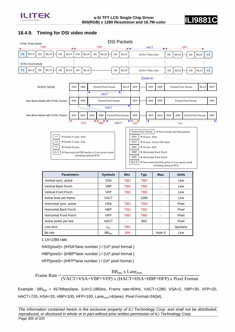
a-Si TFT LCD Single Chip Driver 800(RGB) x 1280 Resolution and 16.7M-color ILI9881C
The information contained herein is the exclusive property of ILI Technology Corp. and shall not be distributed, reproduced, or disclosed in whole or in part without prior written permission of ILI Technology Corp. Page 305 of 320
18.4.9. Timing for DSI video mode
VS HS HS HS HS
BLLPVS HS HS
VSA
VSE HS
VBP
HS HS
VFP
VSActive Video AreaHS
HS HS VSActive Video Area
HBPHSS Packed Pixel Stream BLLP HFP HBPHSS Packed Pixel Stream BLLP HFP
VACT
Zoom in
HACT
tlineHBP HFP
DSI Packets
HBPHSS Packed Pixel Stream HFP HBPHSS Packed Pixel Stream HFP
HACT
HSAHSS Packed Pixel Stream HFP
HACT
HSE HBP HSAHSS Packed Pixel Stream HFPHSE HBPNon-Burst Mode with SYNC Pulses
BURST MODE
Non-Burst Mode with SYNC Events
SYNC Pulse Mode
SYNC Event Mode
HSA
BLLP BLLP BLLP BLLP BLLP BLLP
BLLP BLLP BLLP BLLP BLLP BLLP
BLLP
BLLP
HSS
HSA
HSE
HBP
HFP
BLLP
Packet Pixel Stream Pixel stream and Null packets
H-sync. Start
H-sync. Active (No data)
H-sync. End
Horizontal Back Porch
Horizontal Front Porch
Non-restricted DSI packet or Low power mode
including optional BTA
Packet V-sync. Start
VSE
VS
HS
BLLP
Packet V-sync. End
Packet H-sync.
Non-restricted DSI packet or Low power mode
including optional BTA
Parameters Symbols Min. Typ. Max. Units
Vertical sync. active VSA TBD TBD - Line
Vertical Back Porch VBP TBD TBD - Line
Vertical Front Porch VFP TBD TBD - Line
Active lines per frame VACT - 1280 - Line
Horizontal sync. active HSA TBD TBD - Pixel
Horizontal Back Porch HBP TBD TBD - Pixel
Horizontal Front Porch HFP TBD TBD - Pixel
Active pixels per line HACT - 800 - Pixel
Line time tline TBD - bps/lane
Bit rate BRbps 200 Note 5 Line
1 UI=1/Bit rate
HAS(pixel)= (tHSA*lane number ) / (UI* pixel format )
HBP(pixel)= (tHBP*lane number ) / (UI* pixel format )
HFP(pixel)= (tHFP*lane number ) / (UI* pixel format )
Frame Rate =BRbps x Lanenum
(VACT+VSA+VBP+VFP) x (HACT+HSA+HBP+HFP) x Pixel Format
Example:BRbps = 457Mbps/lane, 1UI=2.1883ns, Frame rate=60Hz, VACT=1280, VSA=2, VBP=30, VFP=20,
HACT=720, HSA=33, HBP=100, HFP=100, Lanenum=4(lane), Pixel Format=24(bit).

a-Si TFT LCD Single Chip Driver 800(RGB) x 1280 Resolution and 16.7M-color ILI9881C
The information contained herein is the exclusive property of ILI Technology Corp. and shall not be distributed, reproduced, or disclosed in whole or in part without prior written permission of ILI Technology Corp. Page 306 of 320
Note:
1. Lanenum: Date lane of MIPI-DSI.
2. Pixel Format: Please reference to “4.1DSI System Interface”.
3. The formula exists slightly error because of the host-transmission way.
4. The best frame rate setting: 2 data lanes:50~60 Hz / 3 data lanes:50~70 Hz / 4 data lanes:50~70 Hz.
5. Please reference to “Table 39: Limited Clock Channel Speed”
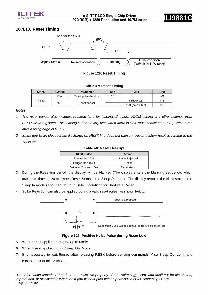
a-Si TFT LCD Single Chip Driver 800(RGB) x 1280 Resolution and 16.7M-color ILI9881C
The information contained herein is the exclusive property of ILI Technology Corp. and shall not be distributed, reproduced, or disclosed in whole or in part without prior written permission of ILI Technology Corp. Page 307 of 320
18.4.10. Reset Timing
Shorter than 5us
tRW
tRT
ResettingNormal operationInitial condition
(Default for H/W reset)
RESX
Display Status
Figure 126: Reset Timing
Table 47: Reset Timing
Signal Symbol Parameter Min Max Unit
RESX
tRW Reset pulse duration 10 uS
tRT Reset cancel 5 (note 1,5) mS
120 (note 1,6,7) mS
Notes:
1. The reset cancel also includes required time for loading ID bytes, VCOM setting and other settings from
EEPROM to registers. This loading is done every time when there is H/W reset cancel time (tRT) within 5 ms
after a rising edge of RESX.
2. Spike due to an electrostatic discharge on RESX line does not cause irregular system reset according to the
Table 48.
Table 48: Reset Descript
RESX Pulse Action
Shorter than 5us Reset Rejected
Longer than 10us Reset
Between 5us and 10us Reset starts
3. During the Resetting period, the display will be blanked (The display enters the blanking sequence, which
maximum time is 120 ms, when Reset Starts in the Sleep Out mode. The display remains the blank state in the
Sleep In mode.) and then return to Default condition for Hardware Reset.
4. Spike Rejection can also be applied during a valid reset pulse, as shown below:
10 us
10 us
Reset is accepted
Less than 20ns width positive spike will be rejected20 ns
Figure 127: Positive Noise Pulse during Reset Low
5. When Reset applied during Sleep In Mode.
6. When Reset applied during Sleep Out Mode.
7. It is necessary to wait 5msec after releasing RESX before sending commands. Also Sleep Out command
cannot be sent for 120msec.

a-Si TFT LCD Single Chip Driver 800(RGB) x 1280 Resolution and 16.7M-color ILI9881C
The information contained herein is the exclusive property of ILI Technology Corp. and shall not be distributed, reproduced, or disclosed in whole or in part without prior written permission of ILI Technology Corp. Page 308 of 320
19. Panel Application
19.1. Input Power Type ILI9881C supports 3 kinds of input power type as shown below.
Table 49: Different Input Power Type
Setting Input Power Type
Power Mode 2A
BOOSTM[2:0] = 1h
DI_PWR_REG = 0h
VSP DC-to-DC
VCI
VSP
VSN
EXTP
EXTN
VDDI
VSN
VSP VSN
VDDI
Power Mode 3
BOOSTM[2:0] = 2h
DI_PWR_REG = don‟t care
ILI4003
VCI
C1P
VSP
C1N
C2P
VSN
C2N
C3P
CTRL_A
C3N
CTRL_B
VCI
VDDI
DC-to-DC
VCI
VSP
VSN
EXTP
EXTN
VCI VDDI
Power Mode 4
BOOSTM[2:0] = 1h
DI_PWR_REG = 1h
VSP DC-to-DC
VCI
VSP
VSN
EXTP
EXTN
VDDI
VSN
VCI
VSP VSN
VCI VDDI
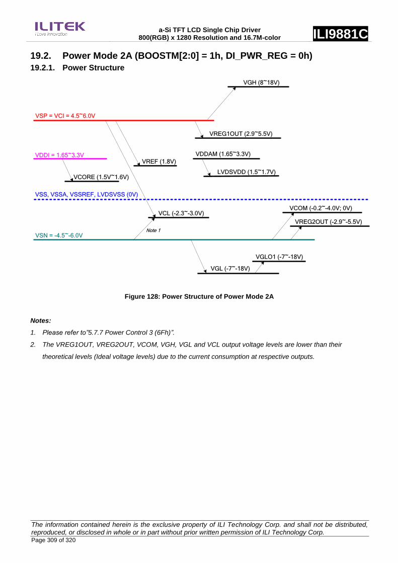
a-Si TFT LCD Single Chip Driver 800(RGB) x 1280 Resolution and 16.7M-color ILI9881C
The information contained herein is the exclusive property of ILI Technology Corp. and shall not be distributed, reproduced, or disclosed in whole or in part without prior written permission of ILI Technology Corp. Page 309 of 320
19.2. Power Mode 2A (BOOSTM[2:0] = 1h, DI_PWR_REG = 0h)
19.2.1. Power Structure
VDDI = 1.65~3.3V
VGL (-7~-18V)
VCORE (1.5V~1.6V)
VREF (1.8V)
VDDAM (1.65~3.3V)
LVDSVDD (1.5~1.7V)
VSS, VSSA, VSSREF, LVDSVSS (0V)
VSP = VCI = 4.5~6.0V
VGH (8~18V)
VREG1OUT (2.9~5.5V)
VSN = -4.5~-6.0V
VREG2OUT (-2.9~-5.5V)
VCL (-2.3~-3.0V)VCOM (-0.2~-4.0V; 0V)
VGLO1 (-7~-18V)
Note 1
Figure 128: Power Structure of Power Mode 2A
Notes:
1. Please refer to”5.7.7 Power Control 3 (6Fh)”.
2. The VREG1OUT, VREG2OUT, VCOM, VGH, VGL and VCL output voltage levels are lower than their
theoretical levels (Ideal voltage levels) due to the current consumption at respective outputs.

a-Si TFT LCD Single Chip Driver 800(RGB) x 1280 Resolution and 16.7M-color ILI9881C
The information contained herein is the exclusive property of ILI Technology Corp. and shall not be distributed, reproduced, or disclosed in whole or in part without prior written permission of ILI Technology Corp. Page 310 of 320
19.2.2. Reference Circuit
Fa
ce
Up
(Bu
mp
Vie
w)
D0N
D0P
D1N
D1P
CLKN
CLKP
D2N
D2P
D3N
D3P
VDDI
RESX
TELEDPWM
IM0
IM1IM2RS0
RS1
LANSEL
MTP_PWR
VSP
VGLO1
VGL
VGH
C24P
C23P
C22N
C21N
C41P
C42P
VCL
VREF
VREG1OUT
VDDI
VCORE
LVDSVDD
VCOM
D1
VREG2OUT
C41N
C42N
C21P
C22P
C23N
C24N
Note. VCI and VCIREF pad must be connected to VSP pad.
VSN
VSP
VSN
DUMMY1DUMMY1GOUT_L1GOUT_L2GOUT_L3GOUT_L4GOUT_L5GOUT_L6GOUT_L7GOUT_L8GOUT_L9GOUT_L10GOUT_L11GOUT_L12GOUT_L13GOUT_L14GOUT_L15GOUT_L16GOUT_L17GOUT_L18GOUT_L19GOUT_L20GOUT_L21GOUT_L22VCOMVCOMVCOM
VSSAVSSAVSSAVSSAVSSAVSSAVSSAVSSAVSSAVSSAVTESTOUTPVTESTOUTPLVDSVSSD0ND0ND0ND0ND0ND0ND0PD0PD0PD0PD0PD0PLVDSVSSD1ND1ND1ND1ND1ND1ND1PD1PD1PD1PD1PD1PLVDSVSSCLKNCLKNCLKNCLKNCLKNCLKNCLKPCLKPCLKPCLKPCLKPCLKPLVDSVSSD2ND2ND2ND2ND2ND2ND2PD2PD2PD2PD2PD2PLVDSVSSD3ND3ND3ND3ND3ND3ND3PD3PD3PD3PD3PD3PLVDSVSSLVDSVSSLVDSVSSLVDSVSSLVDSVSSLVDSVSSLVDSVSSLVDSVSSLVDSVSSLVDSVSSLVDSVSSLVDSVSSLVDSVDDLVDSVDDLVDSVDDLVDSVDDLVDSVDDLVDSVDDLVDSVDDLVDSVDDLVDSVDDLVDSVDDLVDSVDDLVDSVDDVDDAMVDDAMVDDAMVDDAMVDDAMVDDAMVDDAMVDDAMVDDAMVDDAMVDDAMVDDAMVCC1VCC1VCC1VCC1VCC1VCC1VCC1VCC1VCC1VCC1VCC1VCC1VCC1VCC1VCC1VCOREVCOREVCOREVCOREVCOREVCOREVCOREVCOREVCOREVCOREVCOREVCOREVCOREVCOREVCOREVSSVSSVSSVSSVSSVSSVSSVSSVSSVSSVSSVSSVSSVSSVSSTOUT3TOUT3TOUT2TOUT2TOUT1TOUT1TOUT0TOUT0DUMMYPDUMMYPDUMMYPDUMMYPDUMMYPDUMMYPDUMMYPDUMMYPDUMMYPDUMMYPDUMMYPDUMMYPDUMMYPDUMMYPDUMMYPDUMMYPDUMMYPDUMMYPDUMMYPDUMMYPDUMMYPDUMMYPDUMMYPDUMMYPDUMMYPDUMMYPDUMMYPDUMMYPDUMMYPDUMMYPDUMMYPDUMMYPDUMMYPDUMMYPDUMMYPDUMMYPDUMMYPDUMMYPDUMMYPDUMMYPDUMMYPDUMMYPDUMMYPDUMMYPDUMMYPVSSVSSD7D7D6D6D5D5D4D4D3D3D2D2D1D1D0D0HSHSVSVSVSSDUMMYVSSDUMMYPCLKPCLKDCXDCXCSXCSXSCLSCLSDISDISDOSDOLEDPWMLEDPWMLEDPWMLEDPWMTETETETETETETE1TE1TE1TE1TE1TE1RESXRESXRESXRESXTEST5TEST4TEST3TEST2TEST1TEST0VSSDUMMYVSSDUMMYIM0IM0VDDIVDDIIM1IM1IM2IM2RS0RS0VDDIVDDIRS1RS1VSSVSSLANSELLANSELVDDIVDDIBOOSTM0BOOSTM0BOOSTM2BOOSTM2BOOSTM1BOOSTM1VCC2VCC2VCC2VCC2VCC2VCC2VCC2VCC2VCC2VCC2VCOREVCOREVCOREVCOREVCOREVCOREVCOREVCOREVCOREVCOREVSSVSSVSSVSSVSSVSSVSSVSSVSSVSSEXTNEXTNEXTNEXTNEXTNEXTNEXTNEXTNEXTPEXTPEXTPEXTPEXTPEXTPEXTPEXTPMTP_PWRMTP_PWRMTP_PWRMTP_PWRMTP_PWRMTP_PWRDUMMYNDUMMYNVCIREFVCIREFVCIREFVCIREFVCIREFVTESTOUTNVTESTOUTNDUMMYNDUMMYNDUMMYNDUMMYNDUMMYNDUMMYNVSSREFVSSREFVSSREFVSSREFVSSAVSSAVSSAVSSAVSSAVSSAVSSAVREG1OUTVREG1OUTVREG1OUTVREG2OUTVREG2OUTVREG2OUTVREFVREFVREFVSSVSSVSSVSSVSSVCIVCIVCIVCIVCIVCIVCIVCIVCLVCLVCLVCLVCLC41PC41PC41PC41PC41PC41PC41PC41NC41NC41NC41NC41NC41NC41NC42PC42PC42PC42PC42PC42PC42PC42NC42NC42NC42NC42NC42NC42NVSPVSPVSPVSPVSPVSPVSPVSNVSNVSNVSNVSNVSNVSNC21NC21NC21NC21NC21NC21NC21NC21PC21PC21PC21PC21PC21PC21PC22NC22NC22NC22NC22NC22NC22NC22PC22PC22PC22PC22PC22PC22PVGHVGHVGHVGHVGHVGHVCIVCIVCIVCIVCIVCIVSSVSSVSSVSSVSSVSSVSSVSSC23PC23PC23PC23PC23PC23PC23PC23NC23NC23NC23NC23NC23NC23NC24PC24PC24PC24PC24PC24PC24PC24NC24NC24NC24NC24NC24NC24NVGLVGLVGLVGLVGLVGLC31PC31PC31PC31PC31PC31PC31PVGLO2DUMMYVGLO2DUMMYVGLO2DUMMYVGLO2DUMMYVGLO2DUMMYVGLO2DUMMYVGLO2DUMMYVGLO1VGLO1VGLO1VGLO1VGLO1VGLO1VCOMRVCOMRDUMMYR1DUMMYR1
VCOMVCOMVCOMGOUT_R22GOUT_R21GOUT_R20GOUT_R19GOUT_R18GOUT_R17GOUT_R16GOUT_R15GOUT_R14GOUT_R13GOUT_R12GOUT_R11GOUT_R10GOUT_R9GOUT_R8GOUT_R7GOUT_R6GOUT_R5GOUT_R4GOUT_R3GOUT_R2GOUT_R1DUMMY2DUMMY2
Figure 129: Reference Circuit of Power Mode 2A

a-Si TFT LCD Single Chip Driver 800(RGB) x 1280 Resolution and 16.7M-color ILI9881C
The information contained herein is the exclusive property of ILI Technology Corp. and shall not be distributed, reproduced, or disclosed in whole or in part without prior written permission of ILI Technology Corp. Page 311 of 320
19.2.3. External Component
Table 50: External Component table of Power Mode 2A
N0. Pad Name Typical Value Note
1 VDDI 1.0uF / 4V I/O and Digital Power
2 VSP 2.2~4.7uF / 10V Analog Power
3 VSN 2.2~4.7uF / 10V Analog Power
4 LVDSVDD 1.0uF / 4V
5 VCORE 2.2uF / 4V
6 VREF 1.0uF / 4V Optional
7 VCL 1.0uF / 6.3V
8 REG1OUT 1.0uF / 6.3V Optional
9 REG2OUT 1.0uF / 6.3V Optional
10 VCOM 2.2uF / 4V
11 VGH 1.0uF / 25V
12 VGL 1.0uF / 25V
13 VGLO1 1.0uF / 25V Optional
(if not used)
14 C21P/C21N 1.0uF / 25V
15 C22P/C22N 1.0uF / 25V Optional
16 C23P/C23N 1.0uF / 25V
17 C24P/C24N 1.0uF / 25V Optional
18 C41P/C41N 1.0uF / 6.3V Optional
19 C42P/C42N 1.0uF / 6.3V Optional
20 D1 Schottky Diode
VF ≤ 0.4V/20mA at 25℃, VR ≥ 30V

a-Si TFT LCD Single Chip Driver 800(RGB) x 1280 Resolution and 16.7M-color ILI9881C
The information contained herein is the exclusive property of ILI Technology Corp. and shall not be distributed, reproduced, or disclosed in whole or in part without prior written permission of ILI Technology Corp. Page 312 of 320
19.3. Power Mode 3 (BOOSTM[2:0] = 2h, DI_PWR_REG = don’t care)
19.3.1. Power Structure
VCI = 2.5~3.3V
VDDI = 1.65~3.3V
VGL (-7~-18V)
VREF (1.8V)
VDDAM (1.65~3.3V)
LVDSVDD (1.5~1.7V)
VSS, VSSA, VSSREF, LVDSVSS (0V)
VSP (4.5~6.0V)
VGH (8~18V)
ILI4
003
VREG1OUT (2.9~5.5V)
ILI4
003
VSN (-4.5~-6.0V)
VREG2OUT (-2.9~-5.5V)
VCL (-2.3~-3.0V)VCOM (-0.2~-4.0V; 0V)
VGLO1 (-7~-18V)
VCORE (1.5V~1.6V)
Note 1
Figure 130: Power Structure of Power Mode 3
Notes:
1. Please refer to”5.7.7 Power Control 3 (6Fh)”.
2. The VSP, VSN, VREG1OUT, VREG2OUT, VCOM, VGH, VGL and VCL output voltage levels are lower than
their theoretical levels (Ideal voltage levels) due to the current consumption at respective outputs.

a-Si TFT LCD Single Chip Driver 800(RGB) x 1280 Resolution and 16.7M-color ILI9881C
The information contained herein is the exclusive property of ILI Technology Corp. and shall not be distributed, reproduced, or disclosed in whole or in part without prior written permission of ILI Technology Corp. Page 313 of 320
19.3.2. Reference Circuit
VSP
VSN
GND
CTRL_A
CTRL_B
VCI
C3N
C3P
C2N
C2P
C1N
C1PILI4003
VCI
D0N
D0P
D1N
D1P
CLKN
CLKP
D2N
D2P
D3N
D3P
VDDI
RESX
TELEDPWM
IM0
IM1IM2RS0
RS1
LANSEL
MTP_PWR
VGLO1
VGL
VCI
VGH
C24P
C23P
C22N
C21N
C41P
C42P
VCL
VREF
VREG1OUT
VDDI
VCORE
LVDSVDD
VCOM
D1
VREG2OUT
C41N
C42N
C21P
C22P
C23N
C24N
VSN
VSP
C1P
C1N
C2P
C2N
C3P
C3N
Fa
ce
Up
(Bu
mp
Vie
w)
DUMMY1DUMMY1GOUT_L1GOUT_L2GOUT_L3GOUT_L4GOUT_L5GOUT_L6GOUT_L7GOUT_L8GOUT_L9GOUT_L10GOUT_L11GOUT_L12GOUT_L13GOUT_L14GOUT_L15GOUT_L16GOUT_L17GOUT_L18GOUT_L19GOUT_L20GOUT_L21GOUT_L22VCOMVCOMVCOM
VSSAVSSAVSSAVSSAVSSAVSSAVSSAVSSAVSSAVSSAVTESTOUTPVTESTOUTPLVDSVSSD0ND0ND0ND0ND0ND0ND0PD0PD0PD0PD0PD0PLVDSVSSD1ND1ND1ND1ND1ND1ND1PD1PD1PD1PD1PD1PLVDSVSSCLKNCLKNCLKNCLKNCLKNCLKNCLKPCLKPCLKPCLKPCLKPCLKPLVDSVSSD2ND2ND2ND2ND2ND2ND2PD2PD2PD2PD2PD2PLVDSVSSD3ND3ND3ND3ND3ND3ND3PD3PD3PD3PD3PD3PLVDSVSSLVDSVSSLVDSVSSLVDSVSSLVDSVSSLVDSVSSLVDSVSSLVDSVSSLVDSVSSLVDSVSSLVDSVSSLVDSVSSLVDSVDDLVDSVDDLVDSVDDLVDSVDDLVDSVDDLVDSVDDLVDSVDDLVDSVDDLVDSVDDLVDSVDDLVDSVDDLVDSVDDVDDAMVDDAMVDDAMVDDAMVDDAMVDDAMVDDAMVDDAMVDDAMVDDAMVDDAMVDDAMVCC1VCC1VCC1VCC1VCC1VCC1VCC1VCC1VCC1VCC1VCC1VCC1VCC1VCC1VCC1VCOREVCOREVCOREVCOREVCOREVCOREVCOREVCOREVCOREVCOREVCOREVCOREVCOREVCOREVCOREVSSVSSVSSVSSVSSVSSVSSVSSVSSVSSVSSVSSVSSVSSVSSTOUT3TOUT3TOUT2TOUT2TOUT1TOUT1TOUT0TOUT0DUMMYPDUMMYPDUMMYPDUMMYPDUMMYPDUMMYPDUMMYPDUMMYPDUMMYPDUMMYPDUMMYPDUMMYPDUMMYPDUMMYPDUMMYPDUMMYPDUMMYPDUMMYPDUMMYPDUMMYPDUMMYPDUMMYPDUMMYPDUMMYPDUMMYPDUMMYPDUMMYPDUMMYPDUMMYPDUMMYPDUMMYPDUMMYPDUMMYPDUMMYPDUMMYPDUMMYPDUMMYPDUMMYPDUMMYPDUMMYPDUMMYPDUMMYPDUMMYPDUMMYPDUMMYPVSSVSSD7D7D6D6D5D5D4D4D3D3D2D2D1D1D0D0HSHSVSVSVSSDUMMYVSSDUMMYPCLKPCLKDCXDCXCSXCSXSCLSCLSDISDISDOSDOLEDPWMLEDPWMLEDPWMLEDPWMTETETETETETETE1TE1TE1TE1TE1TE1RESXRESXRESXRESXTEST5TEST4TEST3TEST2TEST1TEST0VSSDUMMYVSSDUMMYIM0IM0VDDIVDDIIM1IM1IM2IM2RS0RS0VDDIVDDIRS1RS1VSSVSSLANSELLANSELVDDIVDDIBOOSTM0BOOSTM0BOOSTM2BOOSTM2BOOSTM1BOOSTM1VCC2VCC2VCC2VCC2VCC2VCC2VCC2VCC2VCC2VCC2VCOREVCOREVCOREVCOREVCOREVCOREVCOREVCOREVCOREVCOREVSSVSSVSSVSSVSSVSSVSSVSSVSSVSSEXTNEXTNEXTNEXTNEXTNEXTNEXTNEXTNEXTPEXTPEXTPEXTPEXTPEXTPEXTPEXTPMTP_PWRMTP_PWRMTP_PWRMTP_PWRMTP_PWRMTP_PWRDUMMYNDUMMYNVCIREFVCIREFVCIREFVCIREFVCIREFVTESTOUTNVTESTOUTNDUMMYNDUMMYNDUMMYNDUMMYNDUMMYNDUMMYNVSSREFVSSREFVSSREFVSSREFVSSAVSSAVSSAVSSAVSSAVSSAVSSAVREG1OUTVREG1OUTVREG1OUTVREG2OUTVREG2OUTVREG2OUTVREFVREFVREFVSSVSSVSSVSSVSSVCIVCIVCIVCIVCIVCIVCIVCIVCLVCLVCLVCLVCLC41PC41PC41PC41PC41PC41PC41PC41NC41NC41NC41NC41NC41NC41NC42PC42PC42PC42PC42PC42PC42PC42NC42NC42NC42NC42NC42NC42NVSPVSPVSPVSPVSPVSPVSPVSNVSNVSNVSNVSNVSNVSNC21NC21NC21NC21NC21NC21NC21NC21PC21PC21PC21PC21PC21PC21PC22NC22NC22NC22NC22NC22NC22NC22PC22PC22PC22PC22PC22PC22PVGHVGHVGHVGHVGHVGHVCIVCIVCIVCIVCIVCIVSSVSSVSSVSSVSSVSSVSSVSSC23PC23PC23PC23PC23PC23PC23PC23NC23NC23NC23NC23NC23NC23NC24PC24PC24PC24PC24PC24PC24PC24NC24NC24NC24NC24NC24NC24NVGLVGLVGLVGLVGLVGLC31PC31PC31PC31PC31PC31PC31PVGLO2DUMMYVGLO2DUMMYVGLO2DUMMYVGLO2DUMMYVGLO2DUMMYVGLO2DUMMYVGLO2DUMMYVGLO1VGLO1VGLO1VGLO1VGLO1VGLO1VCOMRVCOMRDUMMYR1DUMMYR1
VCOMVCOMVCOMGOUT_R22GOUT_R21GOUT_R20GOUT_R19GOUT_R18GOUT_R17GOUT_R16GOUT_R15GOUT_R14GOUT_R13GOUT_R12GOUT_R11GOUT_R10GOUT_R9GOUT_R8GOUT_R7GOUT_R6GOUT_R5GOUT_R4GOUT_R3GOUT_R2GOUT_R1DUMMY2DUMMY2
Figure 131: Reference Circuit of Power Mode 3

a-Si TFT LCD Single Chip Driver 800(RGB) x 1280 Resolution and 16.7M-color ILI9881C
The information contained herein is the exclusive property of ILI Technology Corp. and shall not be distributed, reproduced, or disclosed in whole or in part without prior written permission of ILI Technology Corp. Page 314 of 320
19.3.3. External Component
Table 51: External Component table of Power Mode 3
N0. Pad Name Typical Value Note
1 VCI 1.0uF / 6.3V Analog Power
2 VDDI 1.0uF / 4V I/O and Digital Power
3 VSP 2.2~4.7uF / 6.3V
4 VSN 2.2~4.7uF / 6.3V
5 LVDSVDD 1.0uF / 4V
6 VCORE 2.2uF / 4V
7 VREF 1.0uF / 4V Optional
8 VCL 1.0uF / 6.3V
9 REG1OUT 1.0uF / 6.3V Optional
10 REG2OUT 1.0uF / 6.3V Optional
11 VCOM 2.2uF / 4V
12 VGH 1.0uF / 25V
13 VGL 1.0uF / 25V
14 VGLO1 1.0uF / 25V Optional
(if not used)
15 C21P/C21N 1.0uF / 25V
16 C22P/C22N 1.0uF / 25V Optional
17 C23P/C23N 1.0uF / 25V
18 C24P/C24N 1.0uF / 25V Optional
19 C41P/C41N 1.0uF / 6.3V Optional
20 C42P/C42N 1.0uF / 6.3V Optional
21 Q1 ILI4003
22 C1P/C1N 2.2uF / 6.3V
23 C2P/C2N 2.2uF / 6.3V
24 C3P/C3N 2.2uF / 6.3V
25 D1 Schottky Diode
VF ≤ 0.4V/20mA at 25℃, VR ≥ 30V

a-Si TFT LCD Single Chip Driver 800(RGB) x 1280 Resolution and 16.7M-color ILI9881C
The information contained herein is the exclusive property of ILI Technology Corp. and shall not be distributed, reproduced, or disclosed in whole or in part without prior written permission of ILI Technology Corp. Page 315 of 320
19.4. Power Mode 4 (BOOSTM[2:0] = 1h, DI_PWR_REG = 1h)
19.4.1. Power Structure
VCI = 2.5~3.3V
VDDI = 1.65~3.3V
VGL (-7~-18V)
VREF (1.8V)
VDDAM (1.65~3.3V)
LVDSVDD (1.5~1.7V)
VSS, VSSA, VSSREF, LVDSVSS (0V)
VSP = 4.5~6.0V
VGH (8~18V)
VREG1OUT (2.9~5.5V)
VSN = -4.5~-6.0V
VREG2OUT (-2.9~-5.5V)
VCL (-2.3~-3.0V)VCOM (-0.2~-4.0V; 0V)
VGLO1 (-7~-18V)
VCORE (1.5V~1.6V)
Note 1
Figure 132: Power Structure of Power Mode 4
Notes:
1. Please refer to”5.7.7 Power Control 3 (6Fh)”.
2. The VREG1OUT, VREG2OUT, VCOM, VGH, VGL and VCL output voltage levels are lower than their
theoretical levels (Ideal voltage levels) due to the current consumption at respective outputs.

a-Si TFT LCD Single Chip Driver 800(RGB) x 1280 Resolution and 16.7M-color ILI9881C
The information contained herein is the exclusive property of ILI Technology Corp. and shall not be distributed, reproduced, or disclosed in whole or in part without prior written permission of ILI Technology Corp. Page 316 of 320
19.4.2. Reference Circuit
Fa
ce
Up
(Bu
mp
Vie
w)
D0N
D0P
D1N
D1P
CLKN
CLKP
D2N
D2P
D3N
D3P
VDDI
RESX
TELEDPWM
IM0
IM1IM2RS0
RS1
LANSEL
MTP_PWR
VSP
VGLO1
VGL
VGH
C24P
C23P
C22N
C21N
C41P
C42P
VCL
VREF
VREG1OUT
VDDI
VCORE
LVDSVDD
VCOM
D1
VREG2OUT
C41N
C42N
C21P
C22P
C23N
C24N
Note. VCI and VCIREF pad must be connected to VSP pad.
VSN
VSP
VSN
VCI
VCI
DUMMY1DUMMY1GOUT_L1GOUT_L2GOUT_L3GOUT_L4GOUT_L5GOUT_L6GOUT_L7GOUT_L8GOUT_L9GOUT_L10GOUT_L11GOUT_L12GOUT_L13GOUT_L14GOUT_L15GOUT_L16GOUT_L17GOUT_L18GOUT_L19GOUT_L20GOUT_L21GOUT_L22VCOMVCOMVCOM
VSSAVSSAVSSAVSSAVSSAVSSAVSSAVSSAVSSAVSSAVTESTOUTPVTESTOUTPLVDSVSSD0ND0ND0ND0ND0ND0ND0PD0PD0PD0PD0PD0PLVDSVSSD1ND1ND1ND1ND1ND1ND1PD1PD1PD1PD1PD1PLVDSVSSCLKNCLKNCLKNCLKNCLKNCLKNCLKPCLKPCLKPCLKPCLKPCLKPLVDSVSSD2ND2ND2ND2ND2ND2ND2PD2PD2PD2PD2PD2PLVDSVSSD3ND3ND3ND3ND3ND3ND3PD3PD3PD3PD3PD3PLVDSVSSLVDSVSSLVDSVSSLVDSVSSLVDSVSSLVDSVSSLVDSVSSLVDSVSSLVDSVSSLVDSVSSLVDSVSSLVDSVSSLVDSVDDLVDSVDDLVDSVDDLVDSVDDLVDSVDDLVDSVDDLVDSVDDLVDSVDDLVDSVDDLVDSVDDLVDSVDDLVDSVDDVDDAMVDDAMVDDAMVDDAMVDDAMVDDAMVDDAMVDDAMVDDAMVDDAMVDDAMVDDAMVCC1VCC1VCC1VCC1VCC1VCC1VCC1VCC1VCC1VCC1VCC1VCC1VCC1VCC1VCC1VCOREVCOREVCOREVCOREVCOREVCOREVCOREVCOREVCOREVCOREVCOREVCOREVCOREVCOREVCOREVSSVSSVSSVSSVSSVSSVSSVSSVSSVSSVSSVSSVSSVSSVSSTOUT3TOUT3TOUT2TOUT2TOUT1TOUT1TOUT0TOUT0DUMMYPDUMMYPDUMMYPDUMMYPDUMMYPDUMMYPDUMMYPDUMMYPDUMMYPDUMMYPDUMMYPDUMMYPDUMMYPDUMMYPDUMMYPDUMMYPDUMMYPDUMMYPDUMMYPDUMMYPDUMMYPDUMMYPDUMMYPDUMMYPDUMMYPDUMMYPDUMMYPDUMMYPDUMMYPDUMMYPDUMMYPDUMMYPDUMMYPDUMMYPDUMMYPDUMMYPDUMMYPDUMMYPDUMMYPDUMMYPDUMMYPDUMMYPDUMMYPDUMMYPDUMMYPVSSVSSD7D7D6D6D5D5D4D4D3D3D2D2D1D1D0D0HSHSVSVSVSSDUMMYVSSDUMMYPCLKPCLKDCXDCXCSXCSXSCLSCLSDISDISDOSDOLEDPWMLEDPWMLEDPWMLEDPWMTETETETETETETE1TE1TE1TE1TE1TE1RESXRESXRESXRESXTEST5TEST4TEST3TEST2TEST1TEST0VSSDUMMYVSSDUMMYIM0IM0VDDIVDDIIM1IM1IM2IM2RS0RS0VDDIVDDIRS1RS1VSSVSSLANSELLANSELVDDIVDDIBOOSTM0BOOSTM0BOOSTM2BOOSTM2BOOSTM1BOOSTM1VCC2VCC2VCC2VCC2VCC2VCC2VCC2VCC2VCC2VCC2VCOREVCOREVCOREVCOREVCOREVCOREVCOREVCOREVCOREVCOREVSSVSSVSSVSSVSSVSSVSSVSSVSSVSSEXTNEXTNEXTNEXTNEXTNEXTNEXTNEXTNEXTPEXTPEXTPEXTPEXTPEXTPEXTPEXTPMTP_PWRMTP_PWRMTP_PWRMTP_PWRMTP_PWRMTP_PWRDUMMYNDUMMYNVCIREFVCIREFVCIREFVCIREFVCIREFVTESTOUTNVTESTOUTNDUMMYNDUMMYNDUMMYNDUMMYNDUMMYNDUMMYNVSSREFVSSREFVSSREFVSSREFVSSAVSSAVSSAVSSAVSSAVSSAVSSAVREG1OUTVREG1OUTVREG1OUTVREG2OUTVREG2OUTVREG2OUTVREFVREFVREFVSSVSSVSSVSSVSSVCIVCIVCIVCIVCIVCIVCIVCIVCLVCLVCLVCLVCLC41PC41PC41PC41PC41PC41PC41PC41NC41NC41NC41NC41NC41NC41NC42PC42PC42PC42PC42PC42PC42PC42NC42NC42NC42NC42NC42NC42NVSPVSPVSPVSPVSPVSPVSPVSNVSNVSNVSNVSNVSNVSNC21NC21NC21NC21NC21NC21NC21NC21PC21PC21PC21PC21PC21PC21PC22NC22NC22NC22NC22NC22NC22NC22PC22PC22PC22PC22PC22PC22PVGHVGHVGHVGHVGHVGHVCIVCIVCIVCIVCIVCIVSSVSSVSSVSSVSSVSSVSSVSSC23PC23PC23PC23PC23PC23PC23PC23NC23NC23NC23NC23NC23NC23NC24PC24PC24PC24PC24PC24PC24PC24NC24NC24NC24NC24NC24NC24NVGLVGLVGLVGLVGLVGLC31PC31PC31PC31PC31PC31PC31PVGLO2DUMMYVGLO2DUMMYVGLO2DUMMYVGLO2DUMMYVGLO2DUMMYVGLO2DUMMYVGLO2DUMMYVGLO1VGLO1VGLO1VGLO1VGLO1VGLO1VCOMRVCOMRDUMMYR1DUMMYR1
VCOMVCOMVCOMGOUT_R22GOUT_R21GOUT_R20GOUT_R19GOUT_R18GOUT_R17GOUT_R16GOUT_R15GOUT_R14GOUT_R13GOUT_R12GOUT_R11GOUT_R10GOUT_R9GOUT_R8GOUT_R7GOUT_R6GOUT_R5GOUT_R4GOUT_R3GOUT_R2GOUT_R1DUMMY2DUMMY2
Figure 133: Reference Circuit of Power Mode 4

a-Si TFT LCD Single Chip Driver 800(RGB) x 1280 Resolution and 16.7M-color ILI9881C
The information contained herein is the exclusive property of ILI Technology Corp. and shall not be distributed, reproduced, or disclosed in whole or in part without prior written permission of ILI Technology Corp. Page 317 of 320
19.4.3. External Component
Table 52: External Component table of Power Mode 4
N0. Pad Name Typical Value Note
1 VDDI 1.0uF / 4V I/O and Digital Power
2 VCI 1.0uF / 6.3V Analog Power
3 VSP 2.2~4.7uF / 10V Analog Power
4 VSN 2.2~4.7uF / 10V Analog Power
5 LVDSVDD 1.0uF / 4V
6 VCORE 2.2uF / 4V
7 VREF 1.0uF / 4V Optional
8 VCL 1.0uF / 6.3V
9 REG1OUT 1.0uF / 6.3V Optional
10 REG2OUT 1.0uF / 6.3V Optional
11 VCOM 2.2uF / 4V
12 VGH 1.0uF / 25V
13 VGL 1.0uF / 25V
14 VGLO1 1.0uF / 25V Optional
(if not used)
15 C21P/C21N 1.0uF / 25V
16 C22P/C22N 1.0uF / 25V Optional
17 C23P/C23N 1.0uF / 25V
18 C24P/C24N 1.0uF / 25V Optional
19 C41P/C41N 1.0uF / 6.3V Optional
20 C42P/C42N 1.0uF / 6.3V Optional
21 D1 Schottky Diode
VF ≤ 0.4V/20mA at 25℃, VR ≥ 30V

a-Si TFT LCD Single Chip Driver 800(RGB) x 1280 Resolution and 16.7M-color ILI9881C
The information contained herein is the exclusive property of ILI Technology Corp. and shall not be distributed, reproduced, or disclosed in whole or in part without prior written permission of ILI Technology Corp. Page 318 of 320
19.5. Maximum Layout Resistance (TBD)
Table 53: Maximum Layout Resistance
Pad Name Type Maximum
series resistance Unit
VCI Power Supply 5 Ω
VCIREF Power Supply 10 Ω
VDDI Power Supply 5 Ω
VCC1 Power Supply 5 Ω
VCC2 Power Supply 5 Ω
VDDAM Power Supply 5 Ω
VSP Power Supply 5 Ω
VSN Power Supply 5 Ω
VSSA Ground 5 Ω
VSSREF Ground 10 Ω
LVDSVSS Ground 50 Ω
VSS Ground 5 Ω
MTP_PWR Power Supply 5 Ω
VREG1OUT Analog 20 Ω
VERG2OUT Analog 20 Ω
VCL Analog 5 Ω
VGH Analog 10 Ω
VGL Analog 10 Ω
VGLO1 Analog 10 Ω
EXTP Output 10 Ω
EXTN Output 10 Ω
LVDSVDD Analog 5 Ω
VREF Analog 20 Ω
VCORE Analog 5 Ω
C21P, C21N, C22P, C22N C23P, C23N, C24P, C24N C41P, C41N, C42P, C42N C51P, C51N, C52P, C52N
Step-up Capacitor 5 Ω
IM[2:0], RS[1:0] LANSEL, BOOSTM[2:0]
Input 100 Ω
RESX Input 100 Ω
TE, TE1, LEDPWM Output 50 Ω
CLKP, CLKN D1P, D1N D2P, D2N D3P, D3N
Input 5 Ω
D0P, D0N Input + Output 5 Ω
CSX, DCX, SCL, SDI Input 100 Ω
SDO Output 100 Ω
GOUT_L[22:1] GOUT_R[22:1]
Output 10 Ω
VCOM Analog 5 Ω
VTESTOUTP Analog 100 Ω
VTESTOUTN Analog 100 Ω
TOUT[3:0] Input + Output 100 Ω
TEST[3:0] Input + Output 100 Ω
VS, HS Input + Output 100 Ω
PCLK Input 100 Ω
D[7:0] Input + Output 50 Ω
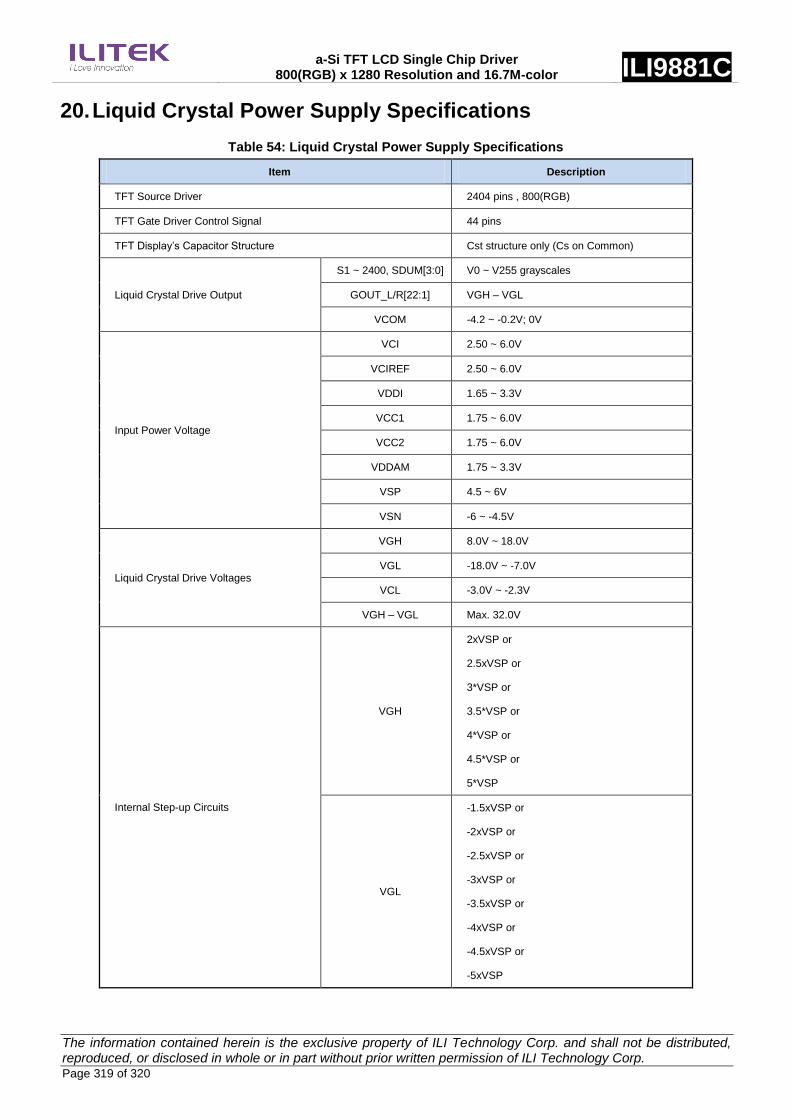
a-Si TFT LCD Single Chip Driver 800(RGB) x 1280 Resolution and 16.7M-color ILI9881C
The information contained herein is the exclusive property of ILI Technology Corp. and shall not be distributed, reproduced, or disclosed in whole or in part without prior written permission of ILI Technology Corp. Page 319 of 320
20. Liquid Crystal Power Supply Specifications
Table 54: Liquid Crystal Power Supply Specifications
Item Description
TFT Source Driver 2404 pins , 800(RGB)
TFT Gate Driver Control Signal 44 pins
TFT Display‟s Capacitor Structure Cst structure only (Cs on Common)
Liquid Crystal Drive Output
S1 ~ 2400, SDUM[3:0] V0 ~ V255 grayscales
GOUT_L/R[22:1] VGH – VGL
VCOM -4.2 ~ -0.2V; 0V
Input Power Voltage
VCI 2.50 ~ 6.0V
VCIREF 2.50 ~ 6.0V
VDDI 1.65 ~ 3.3V
VCC1 1.75 ~ 6.0V
VCC2 1.75 ~ 6.0V
VDDAM 1.75 ~ 3.3V
VSP 4.5 ~ 6V
VSN -6 ~ -4.5V
Liquid Crystal Drive Voltages
VGH 8.0V ~ 18.0V
VGL -18.0V ~ -7.0V
VCL -3.0V ~ -2.3V
VGH – VGL Max. 32.0V
Internal Step-up Circuits
VGH
2xVSP or
2.5xVSP or
3*VSP or
3.5*VSP or
4*VSP or
4.5*VSP or
5*VSP
VGL
-1.5xVSP or
-2xVSP or
-2.5xVSP or
-3xVSP or
-3.5xVSP or
-4xVSP or
-4.5xVSP or
-5xVSP

a-Si TFT LCD Single Chip Driver 800(RGB) x 1280 Resolution and 16.7M-color ILI9881C
The information contained herein is the exclusive property of ILI Technology Corp. and shall not be distributed, reproduced, or disclosed in whole or in part without prior written permission of ILI Technology Corp. Page 320 of 320
21. Revision History
Version No. Date Page Description
V090 2014/07/17 All New created
V091 2014/10/01
29
49
141
149
151
199
213
226
231
281
305
311
314
317
Modify the dummy pad
Modify the description of ULPS
Modify the restriction of command Page0_2Ch
Modify the restriction of command Page0_3Ch
Modify the description of command Page0_45h
Modify the pumping cycle description of commands Page1_41h~43h
Add the command Page1_F0h~F1h
Modify the command address of DSI Lanes Control
Modify the description of command Page4_6Ch
Modify the power on/off sequence
Modify the timing for DSI video mode
Modify the external component table of power mode 2A
Modify the external component table of power mode 3
Modify the external component table of power mode 4
V092 2014/10/16
118
119
120
121
121
122
122
123
123
271
272
288
Add the page 2 command set
Add the page 3 command set
Add the page 4 command set
Add the page 5 command set
Add the page 6 command set
Add the page 7 command set
Add the page 8 command set
Add the page 9 command set
Add the page 10 command set
Add the enter/exit idle mode sequence
Add the bist mode function
Add the internal vgh programming flow