Embed Size (px)
Citation preview

1.2 mW 2.4 GHz PLL for ZigBee and BLE standardin Single-Well 0.18 µm CMOS with efficient divider
architecture
Purushothama Chary P∗ Rizwan Shaik Peerla† Sesha Sairam Regulagadda‡, Mohd Abdul Naseeb§,Amit Acharyya¶ Rajalaksmi P‖ Debashis Mandal∗∗ and Ashudeb Dutta††
Indian Institute of Technology Hyderabad, Arizona State University∗∗,∗[email protected], †[email protected], ‡[email protected], §[email protected],¶amit [email protected], ‖[email protected], ∗∗[email protected], ††asudeb [email protected]
Abstract—This paper proposes a novel single-well VCO inPLL architecture targeting ZigBee (ZB) and Bluetooth LE (BLE)band. It employs PMOS based charge recycling technique inVoltage Controlled Oscillator (VCO) and a Current Mode Logic(CML) divider for I-Q generation in single-well CMOS. Anefficient, low current, Integer-N, Multi Modulus Divider (MMD)using True Single Phase Clock (TSPC) logic is incorporated inthe design to minimize the overall PLL power consumption. TheVCO-CML cell gives phase noise of -147 dBc/Hz at 1 MHz offset.PLL consumes 1.2mW of power at 1.2V supply with a settlingtime less than 45µs and core area is 743µm x 416µm using UMC0.18µm CMOS Mixed Mode Technology.
Keywords—Single well, PLL, LC-VCO, CML, MMD, TSPC,BLE, ZB, Integer-N. 1
I. INTRODUCTION
A major portion of power consumption in moderntransceivers such as BLE and ZigBee is from frequencysynthesizers. A strong research work is going on for reducingthe power consumption of synthesizers. Prominent methodsare (a) Operating the transistor in subthreshold mode (lowersthe supply current), (b) utilize lower technology node (lowersupply voltage) and (c) scaling down supply voltage withmultiple blocks in the stack.
However, at high frequency, performance optimization be-comes more complex in subthreshold operation. On the otherhand, lower technology designs are costly and do not leadto effective current scaling. So, method (c), mentioned above,may be an effective one for overall power consumption. A highperformance charge recycling PLL using 0.13 µm CMOS real-ized by stacking VCO and CML has been described in [1]. AnAdaptive Body Biasing (ABB) technique in VCO and stackingit with CML leads to low power consumption. However, theabove structure requires twin-well CMOS process that leadsto more cost. So to counter this, single-well process will be agood solution. Further if the similar design can be achieved inhigher technology node (0.18 µm) with similar performanceand supply voltage (1.2 V), it will be more cost effective. Toachieve this target, we have proposed, an Integer-N PLL withsingle-well PMOS based charge recycling technique VCO-CML I-Q generation cell in 0.18 µm CMOS process (operatingat 1.2V supply). Moreover to minimize the power an efficient
1978-1-5090-0136-1/15/$31.00 2015 IEEE
Fig. 1: Architecture of Proposed PLL.
low current, divider using TSPC logic is incorporated in thedesign with ZigBee and BLE compliance.
The paper is organized as follows. Charge recycling PLLis presented in Section II. Section III deals the individualblocks. Simulation results are presented in Section IV. SectionV concludes and summarizes the results.
II. ARCHITECTURE OF THE PROPOSED PLL
The block diagram of the proposed PLL is shown in Fig.1. The brief description of the system is as follows.
a. A 4.6-5.1GHz LC-VCO is stacked by a CML di-vider to generate quadrature output, operating at2.3-2.55GHz. For lower power dissipation, chargerecycling at low voltage operation is implemented inthe blocks . The changes in Vmid due to changein current can be decreased by making the lowDC resistance path from Vmid to ground[1]. Theproposed topology is PMOS based single-well VCOwhich is optimized for low voltage performance. TheCML divider is designed using low VT transistors towork in low voltage operations.
b. A high speed phase frequency detector (PFD) whichreduces the power consumption and jitter is designed.In PFD, high speed is achieved by detection of bothrising and falling edges of input signals [2].
c. Charge pump circuit which uses a current bypasstechnique that suppresses charge sharing and de-creases the sub-threshold currents is used [3]. A third-order Loop Filter is implemented for this PLL.
2015 IEEE Asia Pacific Conference on Postgraduate Research in Microelectronics and Electronics (PrimeAsia)
17

d. The programmable divider uses TSPC 2/3 cells forless power consumption and higher speed. The outputof the dual modulus prescaler is sampled by thecontrol signal so that the delay of the control signal isconstant regardless of the modulus of the divider[4].
III. PLL ARCHITECTURE
A. Charge Recycling LC-VCO and CML divider
The proposed circuit is shown in Fig. 2. The chosen RFapplication targets the 2.4 GHz ISM band. This requires theVCO to operate nominally at 5 GHz. The VCO is basedon single-well LC-tank oscillator, which consists of two 2.4nH inductors (L) and two body biased PMOS transistors togenerate the differential oscillations. The band selection isdone by Switched Capacitor Array (SCA)which is basicallyused for coarse tuning to extend the frequency range of VCOwhereas varactors are used for fine tuning[5]. The gain of theVCO is around 60 MHz/V. VCO typically consumes 580 µAcurrent at 1.2 V supply.
ABB is used to improve the robustness of the VCO toprocess variations and avoids worst-case design. The ideabehind this is to sense the amplitude of the output of VCOand feed it back to the negative trans-conductance cell (M3-M4) making this output amplitude control the body biasaccordingly. This automatically maintains the VCO oscillationsin worst conditions. In [6], ABB technique is implemented tocontrol the body bias of NMOSs. However, in the proposeddesign, it is used for PMOSs.
The CML divider is generally a divide by two divider usedfor differential to quadrature generation. The differential outputof the VCO is fed to the input of the CML divider to generaterequired output. This divider acts as the tail current source tothe VCO.
B. Programmable Frequency Divider
The proposed divider structure is shown in Fig. 3. To designa divider to work in both standards (ZigBee and BLE), thefollowing process is adopted.
a. A crystal oscillator frequency of 10 MHz is chosensuch that it works for both standards. A novel struc-ture that uses separate divider stages after the crystaloscillator to produce both the reference signals isdesigned. Based upon the selection pin of the MUXat the output of these dividers, the reference signal tothe PLL is decided.
b. Mlti modulus divider having 2/3 cells using TSPClogic, are implemented. The internal topological de-tails of the 2/3 cell are shown in Fig. 4. The combina-tional logic, except for an inverter, is absorbed insidethe flop to reduce propagation delay and currentconsumption.
c. The division ratio for Bluetooth LE is 1200 to 1240.So ten 2/3 cells are required whereas only eight cellsare required for ZigBee (480 to 496). So, the outputof the eighth cell is taken as the output of the ZigBeedivider. But the modulus in (MIN) pin of the last 2/3cell of the divider should be grounded. In ZigBeecase, it is not possible.
Fig. 2: Circuit of proposed charge recycling VCO with CMLdivider for quadrature output.
Fig. 3: Block diagram of the proposed programmable divider
(a) TSPC 2/3 cell (b) TSPC flop
Fig. 4: TSPC cell
2015 IEEE Asia Pacific Conference on Postgraduate Research in Microelectronics and Electronics (PrimeAsia)
18
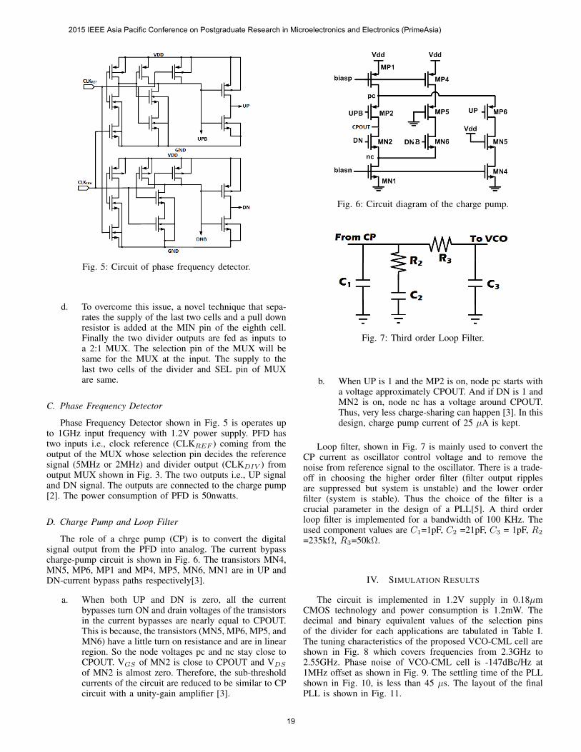
Fig. 5: Circuit of phase frequency detector.
d. To overcome this issue, a novel technique that sepa-rates the supply of the last two cells and a pull downresistor is added at the MIN pin of the eighth cell.Finally the two divider outputs are fed as inputs toa 2:1 MUX. The selection pin of the MUX will besame for the MUX at the input. The supply to thelast two cells of the divider and SEL pin of MUXare same.
C. Phase Frequency Detector
Phase Frequency Detector shown in Fig. 5 is operates upto 1GHz input frequency with 1.2V power supply. PFD hastwo inputs i.e., clock reference (CLKREF ) coming from theoutput of the MUX whose selection pin decides the referencesignal (5MHz or 2MHz) and divider output (CLKDIV ) fromoutput MUX shown in Fig. 3. The two outputs i.e., UP signaland DN signal. The outputs are connected to the charge pump[2]. The power consumption of PFD is 50nwatts.
D. Charge Pump and Loop Filter
The role of a chrge pump (CP) is to convert the digitalsignal output from the PFD into analog. The current bypasscharge-pump circuit is shown in Fig. 6. The transistors MN4,MN5, MP6, MP1 and MP4, MP5, MN6, MN1 are in UP andDN-current bypass paths respectively[3].
a. When both UP and DN is zero, all the currentbypasses turn ON and drain voltages of the transistorsin the current bypasses are nearly equal to CPOUT.This is because, the transistors (MN5, MP6, MP5, andMN6) have a little turn on resistance and are in linearregion. So the node voltages pc and nc stay close toCPOUT. VGS of MN2 is close to CPOUT and VDSof MN2 is almost zero. Therefore, the sub-thresholdcurrents of the circuit are reduced to be similar to CPcircuit with a unity-gain amplifier [3].
Fig. 6: Circuit diagram of the charge pump.
Fig. 7: Third order Loop Filter.
b. When UP is 1 and the MP2 is on, node pc starts witha voltage approximately CPOUT. And if DN is 1 andMN2 is on, node nc has a voltage around CPOUT.Thus, very less charge-sharing can happen [3]. In thisdesign, charge pump current of 25 µA is kept.
Loop filter, shown in Fig. 7 is mainly used to convert theCP current as oscillator control voltage and to remove thenoise from reference signal to the oscillator. There is a trade-off in choosing the higher order filter (filter output ripplesare suppressed but system is unstable) and the lower orderfilter (system is stable). Thus the choice of the filter is acrucial parameter in the design of a PLL[5]. A third orderloop filter is implemented for a bandwidth of 100 KHz. Theused component values are C1=1pF, C2 =21pF, C3 = 1pF, R2
=235kΩ, R3=50kΩ.
IV. SIMULATION RESULTS
The circuit is implemented in 1.2V supply in 0.18µmCMOS technology and power consumption is 1.2mW. Thedecimal and binary equivalent values of the selection pinsof the divider for each applications are tabulated in Table I.The tuning characteristics of the proposed VCO-CML cell areshown in Fig. 8 which covers frequencies from 2.3GHz to2.55GHz. Phase noise of VCO-CML cell is -147dBc/Hz at1MHz offset as shown in Fig. 9. The settling time of the PLLshown in Fig. 10, is less than 45 µs. The layout of the finalPLL is shown in Fig. 11.
2015 IEEE Asia Pacific Conference on Postgraduate Research in Microelectronics and Electronics (PrimeAsia)
19

Fig. 8: Post layout Tuning characteristics of proposed VCO-CML cell.
Fig. 9: Phase noise plot of proposed VCO-CML cell.
Fig. 10: Post layout Settling time plot of proposed PLL.
Fig. 11: Layout of proposed PLL.
TABLE I: Division Ratio of ZigBee and BLE
Selection Pins (P1 P2...P10) Decimal Value Application0011110000 480
to to ZigBee0011111000 4960010110000 1200
to to Bluetooth LE0011011000 1240
TABLE II: Performance Comparison with other PLLs
Parameter [1] [5] This WorkSupply 1.2V 1.2V 1.2V
Technology 0.13 µm 0.18 µm 0.18 µmArchitecture Fractional-N Integer-N Integer-N
Power 860µW 7.95mW 1.2mWFrequency Range 2.5GHz 2.4-2.4835GHz 2.3-2.55GHz
Phase Noise at 1MHz -113.5 dBc/Hz -108.55dBc/Hz -147 dBc/HzSettling Time N/A <25µs <45µs
V. CONCLUSION
2.4-2.48GHz fully-integrated Integer-N PLL with single-well PMOS based charge recycling technique VCO-CML I-Q generation cell in UMC 0.18 µm CMOS process hasbeen implemented. It is compliant to ZigBee and Bluetoothstandards. The performance comparison is in Table II. Powerconsumption is 1.2mW with 1.2V supply. As per our knowl-edge this is most power effective design in 0.18 µm CMOStechnology. The area occupied is 743m x 416m.
REFERENCES
[1] Dongmin Park, Woojae Lee, Sehyung Jeon and SeongHwan Cho,“A 2.5-GHz 860µW Charge-Recycling Fractional-N Frequency Syn-thesizer in 130nm CMOS,” Symposium on VLSI Circuits Digest ofTechnical Papers, pp. 88-89 2008.
[2] Kruti P. Thakore, Harikrishna P. Parmar, N.M.Devashrayee, “LowPower and Low Jitter Phase Frequency Detector for Phase Lock Loop,”International Journal of Engineering Science and Technology pp. 1998-2004 2011.
[3] Yongsam Moon, “A Low-Jitter Phase-Locked Loop Based on a ChargePump Using a Current-Bypass Technique,” Journal Of SemiconductorTechnology and Science, Vol.14, No.3, pp. 331-338 2014.
[4] Saravanan Kathiah, Sankaran Aniruddhan, “Replica Bias Schemefor Efficient Power Utilization in High-Frequency CMOS DigitalCircuits,” IEEE International Symposium on Circuits and Systems(ISCAS), pp. 1002-1005, 2014.
[5] Debashis Mandal, T. K. Bhattacharyya, “7.95mW 2.4GHz Fully-Integrated CMOS Integer-N Frequency Synthesizer,” 20th InternationalConference on VLSI Design 2007.
[6] Dongmin Park, SeongHwan Cho “A 1.8 V 900 /muW 4.5 GHzVCO and Prescaler in 0.18 /mum CMOS Using Charge-RecyclingTechnique,” IEEE Microwave and Wireless Components Letters, Vol.19, No. 2, 2009.
2015 IEEE Asia Pacific Conference on Postgraduate Research in Microelectronics and Electronics (PrimeAsia)
20