Embed Size (px)
Citation preview
14
E-TSPC: Extended True Single-PhaseClock CMOS circuit technique
J. Navarro S.Jr. and W.A.M. Van Noije" LSI/PEE, Escola Politecnica of University of Siio Paulo A v. Prof. Luciano Gualberto, 158, trav. 3, 05508-900 Silo Paulo, S.P.,Brazil, telephone: + 55-11-818 5668 e-mail: [email protected], [email protected]
Abstract The Extended True Single-Phase-Clock (E-TSPC}, an extension of the TSPC CMOS circuit technique, is proposed and analysed. This technique consists of a set of composition rules to build CMOS single-phase circuits. The composition rules are provided to avoid race problems and to preserve data during the holding phases. The used CMOS blocks are the conventional static CMOS logic, nip dynamic logic, n/p latch, data precharged, and the new N-MOS like blocks. Design results show that the E-TSPC can achieve 70% speed improvements, comparing with conventional TSPC techniques, and large power and area savings. A complete dual-modulus prescaler (divide-by-1281129) was implemented in a 0.8J.Lm CMOS process, and a 1.61GHz rate was achieved with a 14.2mW power consumption.
Keywords VLSI design, high speed digital CMOS, clock strategy,
1 INTRODUCTION
Several CMOS clocking policies have been proposed to design VLSI systems. The pseudo-two-phase logic was one of the earliest techniques (West, 1985). Later on two-phase logic structures were proposed, like the Domino technique (Krambeck, 1982) and the NORA technique (Goncalves, 1983 and 1984). A single-phase clock policy was first introduced in (Yuan, 1987) (the True Single-Phase-Clock (TSPC)) and subsequently advanced by (Afghahi, 1990).
In this work we introduce and analyse the new Extended True Single-Phase-Clock CMOS circuit technique (E-TSPC). E-TSPC is an extension of the TSPC technique and consists of a full set of composition rules to build CMOS single-phase circuits, which uses static, dynamic, latch, data precharged, and N-MOS like blocks. The
• This work was partially supported by CNPq/PROTEM, FAPESP and Funda~iio Banco do Brasil.
VLSI: Integrated Systems on Silicon R. Reis & L. Claesen (Eds.) QIFIP 1997 Published by Chapman & Hall
166 Part Five High Speed Circuit Techniques
new N-MOS like blocks enhance the capability of the technique, since they allow building p-MOS chains with speed comparable ton-MOS. The result is a powerful technique which permits the design of complex and fast circuits.
Next section presents the main design rules of the E-TSPC technique, the proofs of their correctness, and an exception rule. The new N-MOS like blocks are introduced in section 3. Some design examples are considered in section 4, and the main conclusions are drawn in section 5.
2 COMPOSmON RULES FOR THEE-TSPC CMOS TECHNIQUE
We will present in this section the composition rules for E-TSPC. They were built in a way similar to that of NORA (Goncalves, 1984). The NORA technique is based on
two-phase logic structures, and it uses static, nip-dynamic, and C~OS logic blocks. The composition rules in NORA were provided to avoid race problems. 2.1 Basic CMOS blocks
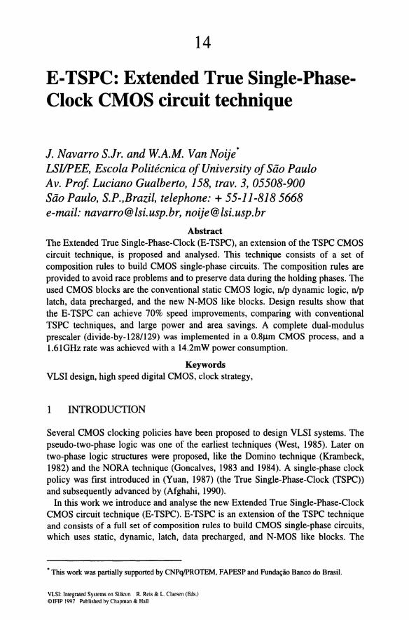
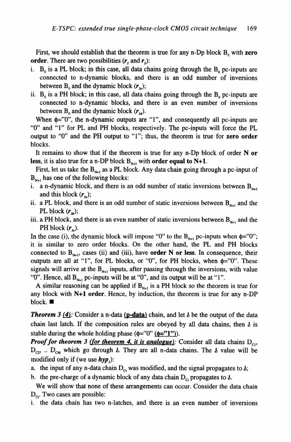
An E-TSPC circuit can use static CMOS logic, nip-dynamic blocks, nip-latches, and high (PH)/low (PL) data precharged blocks (Dp blocks) (Figures 1 and 2) .
.. ~~ ""..:_~L
b) n-c::tvnc:arnlc block c) ~dynarnlc block
d) n-lcrlct'l bloCk e) p-latch block
Figure 1 Construction blocks of the E-TSPC technique.
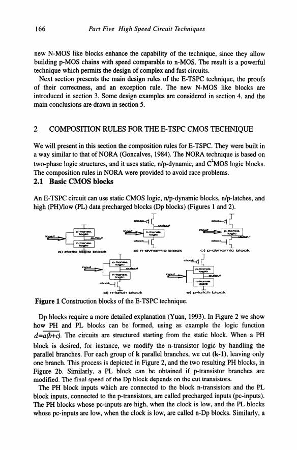
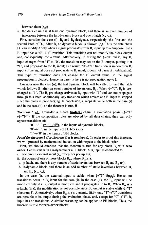
Dp blocks require a more detailed explanation (Yuan, 1993). In Figure 2 we show how PH and PL blocks can be formed, using as example the logic function
d=a(b+c). The circuits are structured starting from the static block. When a PH
block is desired, for instance, we modify the n-transistor logic by handling the parallel branches. For each group of k parallel branches, we cut (k-1), leaving only one branch. This process is depicted in Figure 2, and the two resulting PH blocks, in Figure 2b. Similarly, a PL block can be obtained if p-transistor branches are modified. The final speed of the Dp block depends on the cut transistors.
The PH block inputs which are connected to the block n-transistors and the PL block inputs, connected to the p-transistors, are called precharged inputs (pc-inputs). The PH blocks whose pc-inputs are high, when the clock is low, and the PL blocks whose pc-inputs are low, when the clock is low, are called n-Dp blocks. Similarly, a
E-TSPC: extended true single-phase-clock CMOS circuit technique 167
p-Dp block denotes a PH block with pc-inputs at high or a PL block with pc-inputs at low whenever the clock is h-igh.
d=a(b+c)
b)PHbiOCk:S
a) static CMOS
Figure 2 Transformation from a static block (a) into Dp blocks: (b) PH blocks; (c) PL blocks.
2.2 Composition rules
We will present the composition rules. First, the concept of data chain is done. Definition 1: An-data chain is any not cyclic signal propagation path: 1. containing at least one n-latch, or one n-dynamic, or one n-Dp block; 2. starting in a circuit external input, or in the output of a p-latch, or p-dynamic, or
p-Dp block; when this output is followed by static blocks in the normal data flow, the data chain starts in the output of the last static block;
3. going through static, n-dynamic, n-Dp, or n-latch blocks; 4. regardless of the number and ordering of the blocks defined above; 5. finishing in a circuit external output, or in the input of the first p-latch, or p
dynamic, or p-Dp block. For the p-data chain, equivalent definition applies, changing n by p and vice-versa
everywhere in the definition (we will use x-data chain, where X is nor p). Except for clock skew race, TSPC systems are subject to race errors and
connection limitations, which are equivalent to NORA two-phase race and connection difficulties. Additionally, new connection rules should be incorporated to warrant the correct operation of the nip-latch (Yuan, 1987 and Afghahi, 1990) and the PUPH blocks (Yuan, 1993).
Five composition rules are proposed below for the E-TSPC technique. Any data chain should observe all rules for correct operation. Composition rule 1 (r1): Consider any X-data chain. The X-data chain input should be: an input of a dynamic block, an input of a latch, or a not pc-input of a Dp block.
Composition rule 2 (r ): Consider any X-data chain. A X-latch must not drive,
168 Part Five High Speed Circuit Techniques
directly or through static blocks, aX-dynamic or a x-Dp block. Composition rule 3 (r J: Consider any x-data chain. The number of inversions between: r JtJ. any two adjacent x-dynamic blocks must be odd; r3b. any two adjacent Dp-blocks of the same type must be odd; r 3•• any two adjacent Dp-blocks of complementary types must be even;
rw a PH (PL) block adjacent to an (p)-dynamic (or vice versa) in an (p)-data chain
must be even; r3 •• a PL (PH) block adjacent to an (p)-dynamic (or vice versa) in an (p)-data chain
must be odd. Where two blocks are called adjacent if there are only static blocks between them.
Composition rule 4 (r J: Consider any x-data chain and the last dynamic block in this data chain (when it exists). The number of signal inversions, from this dynamic
block up to at least one X- latch, must be even. Composition rule 5 (r J: Consider any x-data chain. It must have one of the two
configurations: r5•• at least one dynamic block and one latch; rSb" at least two latches and an even number of inversions between them.
2.3 Analysis of r 1-r5 correctness
We will present six theorems which show that when the composition rules r1-r5 are obeyed, no problems due to discharge, pre-charge, and data holding occur. The proofs of the theorems demand two additional hypotheses: Hypothesis 1 (hyp): The clock phases of the system are long enough to permit all
data chain input signals and output of dynamic blocks in holding to propagate up to the data chain outputs. Hypothesis 2 (hyp1): The circuit external inputs should be stable during the evaluation phase of the data chains. Therefore, the external inputs of n-data chains
should be stable when clock= "1" (lj>="l"); the external inputs of p-data chains
should be stable when clock= "0" (lj>="O"). Additionally, a definition of block order is necessary in the theorem proofs.
Definition 2: Consider a Dp or a dynamic block B0 , and the set F= { all x-data
chains which go through B0, where if B0 is an-block, X is n, and if B0 is a p-block, X is p}. We call the number E>(B0)= maximum{(number of x-Dp blocks which
precedes the B0 block in the data chain De) \iDee F} the B0 order. The theorems and their proofs will follow.
Theorem 1 a!: If the composition rules are obeyed by all data chains, then the output of a n-Dp (p-DP) block will reach the
"1" value, for a PL block, or "0" value, for a PH block, after some time in holding phase, and it will keep this value while 11>="0" (cp="l"). Proof for theorem 1 (/or theorem 2. it is analogue): To proof this theorem, we will proceed by mathematical induction with respect to the block order.
E-TSPC: extended true single-phase-clock CMOS circuit technique 169
First, we should establish that the theorem is true for any n-Dp block B0 with zero order. There are two possibilities (r1 and r2):
i. B0 is a PL block; in this case, all data chains going through the B0 pc-inputs are connected to n-dynamic blocks, and there is an odd number of inversions between B0 and the dynamic block (rJ.);
ii. B0 is a PH block; in this case, all data chains going through the B0 pc-inputs are connected to n-dynamic blocks, and there is an even number of inversions between B0 and the dynamic block (rJ).
When cj>="O", then-dynamic outputs are "1", and consequently all pc-inputs are "0" and "1" for PL and PH blocks, respectively. The pc-inputs will force the PL output to "0" and the PH output to "1"; thus, the theorem is true for zero order blocks.
It remains to show that if the theorem is true for any n-Dp block of order N or less, it is also true for a n-DP block BN+I with order equal to N+l.
First, let us take the BN+l as a PL block. Any data chain going through a pc-input of BN+I has one of the following blocks: i. a n-dynamic block, and there is an odd number of static inversions between BN+I
and this block (rJ.); ii. a PL block, and there is an odd number of static inversions between BN+I and the
PL block (r J/J); iii. a PH block, and there is an even number of static inversions between BN+I and the
PH block (rJJ In the case (i), the dynamic block will impose "0" to the BN+I pc-inputs when cp="O"; it is similar to zero order blocks. On the other hand, the PL and PH blocks connected to BN+I' cases (ii) and (iii), have order N or less. In consequence, their outputs are all at "1", for PL blocks, or "0", for PH blocks, when cp="O". These signals will arrive at the BN+I inputs, after passing through the inversions, with value "0". Hence, all BN+I pc-inputs will be at "0", and its output will be at "1".
A similar reasoning can be applied if BN+I is a PH block so the theorem is true for any block with N+l order. Hence, by induction, the theorem is true for any n-DP block. •
Theorem 3 (11.: Consider a n-data (p-data) chain, and let JJ be the output of the data chain last latch. If the composition rules are obeyed by all data chains, then JJ is stable during the whole holding phase (cp="O" (cj!="l")). Proof for theorem 3 (for theorem 4. it is analogue): Consider all data chains Del' DC2, .. DCM which go through JJ. They are all n-data chains. The JJ value will be modified only if (we use hypJ a. the input of any n-data chain De; was modified, and the signal propagates to 1>; b. the pre-charge of a dynamic block of any data chain DCi propagates to 1>.
We will show that none of these arrangements can occur. Consider the data chain De;· Two cases are possible: i. the data chain has two n-latches, and there is an even number of inversions
170 Part Five High Speed Circuit Techniques
between them (r Sb); ii. the data chain has at least one dynamic block, and there is an even number of
inversions between the last dynamic block and one n-latch (r4, r5.).
First, consider the case (i); B1 and B2 designate, respectively, the first and the second latch of De;· After B1 no dynamic block is allowed (rl). Thus the data chain De; can modify JJ only when a signal propagates from B1 input up to h. Suppose that a
B1 input has a "0"~"1" transition. This transition can not modify the block output and, consequently, the h value. Alternatively, if, during the <1>="0" phase, any B1
input changes from "1" to "0", the transition may act on the B1 output, putting it at "1", and propagate to the B2 input; as a result, "0"~"1" transition is imposed on B2
input (if the signal does not propagate to B2 input, it does not cause JJ modification).
This type of transition does not change the B2 output value, so the signal propagation is blocked. Hence, in case (i) there is not propagation up to h.
Consider now the case (ii); the last dynamic block will be called Bl' and the latch which follows B1 after an even number of inversions, B2 • When <1>="0", B1 is precharged at "1". The B1 pre-charge arrives at B2 input with "1" and can not propagate through this latch; additionally, any transition which arrives at a B1 input is stopped since the block is pre-charging. In conclusion, JJ keeps its value both in the case (i)
and in the case (ii), so the theorem is true. •
Theorem 5 M).: Consider a n-data (p-datal chain in evaluation phase (<1>="1" (cj!="O"l). If the composition rules are obeyed by all data chains, then can only appear transitions of:
"0"~"1" ("1"~"0"), in the inputs of dynamic blocks, "0"~"1", in the inputs ofPL blocks, or "1 "~"0" in the inputs of PH blocks.
Proof for theorem 5 ifor theorem 6. it is analope ): In order to proof this theorem, we will proceed by mathematical induction with respect to the block order.
First, we should establish that the theorem is true for any block B0 with zero order. Let us start with an-dynamic or a PL block. A B0 input is connected to: i. one circuit external input (r,, except for pc-inputs); ii. the output of one or more blocks Bo;• where Bo; is a: a. p-latch, and there is any number of static inversions between B0 and B0 ; (r,); b. n-dynamic block, and there is an odd number of static inversions between B0
and Bo; (r 38, r3.);
In the case (i), the external input is stable when <1>="1" (hypz). Hence, no transitions occur in B0 input for the case (i). In the cas~ (ii), the B0 input will be modified only if a Bo; output is modified, and it propagates up to B0• When Bo; is a p-latch, (ii.a), the modification is not possible since Bo; output is stable while <1>="1" (theorem 4). Alternatively, when Bo; is an-dynamic, (ii.b), only "1"~"0" transitions are possible at its output during the evaluation phase, and, except for "0"~"1", B0
input has no transitions. A similar reasoning can be applied to PH blocks. Thus, the theorem is true for zero order blocks.
E-TSPC: extended true single-phase-clock CMOS circuit technique 171
It remains to show that if the theorem is true for any block of order N or less, it is also true for a block BN+t with order equal to N+ 1.
Suppose that BN•t is a n-dynamic or a PL block. A BN+t input is connected to: i. one circuit external input (r,, except for pc-inputs); ii. the output of one or more blocks B01, where B01 is a: a. p-latch, and there is any number of (static) inversions between BN•• and B01 (r,); b. n-dynamic block, and there is an odd number of (static) inversions between BN+t
and B01 (r 111, r3.);
c. PL block, and there is an odd number of (static) inversion between BN+1 and B01
(r 36, r3.);
d. PH block, and there is an even number of (static) inversion between BN+t and B01
(rk, ru)· For the case (i), the reasoning is the same as the zero order blocks. In the case (ii), the BN+t input will be modified only if a B01 output is modified, and it propagates up to BN•t· For (ii.a) and (ii.b), the arguments are also the same as zero order blocks. For (ii.c), B01 has order equal to or less than N, so the inputs of the block have only "0"~"1" transitions; therefore, its output has transitions of "1"~"0", and, due to the odd number of inversions, the BN+t input may have only "0" ~" 1" transitions. In (ii.d), B01 has order equal to or less than N, so its inputs have only "1"~"0" transitions, and again the inputs of BN+t may have only "0" ~" 1" transitions.
A similar reasoning can be applied to PH blocks so the theorem is true for any block with N+l order. Hence, by induction, the theorem is true for any block. • 2.4 Exception rule
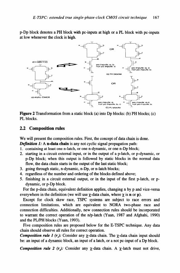
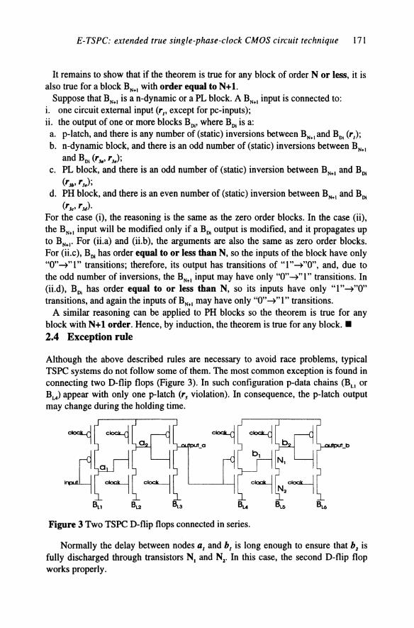
Although the above described rules are necessary to avoid race problems, typical TSPC systems do not follow some of them. The most common exception is found in connecting two D-flip flops (Figure 3). In such configuration p-data chains (Bu or BIA) appear with only one p-latch (r5 violation). In consequence, the p-latch output may change during the holding time.
Figure 3 Two TSPC D-flip flops connected in series.
Normally the delay between nodes a, and b, is long enough to ensure that bz is fully discharged through transistors N1 and N2• In this case, the second D-flip flop works properly.
172 Part Five High Speed Circuit Techniques
We introduce a simple exception rule which covers the D-FF connection case.
Exception rule (r ): Configurations similar to the one of Figure 3, where rules r4 and r5 are not obeyed, are accepted.
3 N-MOS LIKE LOGIC EXTENSION
The given rules allow extremely complex logic designs. When high speed is also a requirement, restrictions on the use of p-dynamic and p-latch blocks should be imposed. These blocks have at least two p-transistors in series, which may considerably reduce the maximum speed. Normally in such applications, the p-data chains are limited to one block, and most logic operations are handled with n-data chains. Of course, when designs are done in this way, part of the rules strengths are lost, and deeper pipelines are necessary.
We can minimise this difficulty and also increase the n-data chain speed by means of N-MOS like blocks. Similar technique was used in (Chang, 1996), but the authors restrained the changes to D-flip flops.
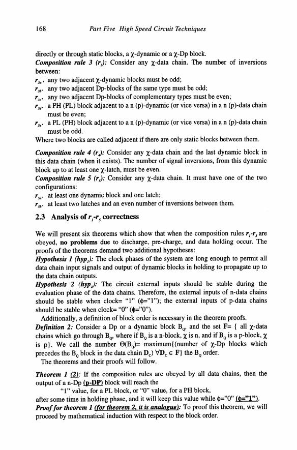
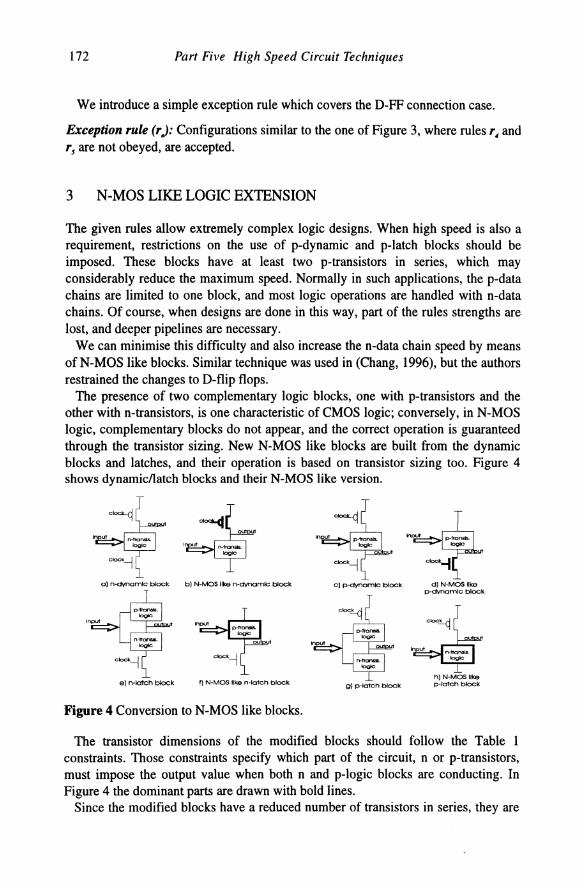
The presence of two complementary logic blocks, one with p-transistors and the other with n-transistors, is one characteristic of CMOS logic; conversely, in N-MOS logic, complementary blocks do not appear, and the correct operation is guaranteed through the transistor sizing. New N-MOS like blocks are built from the dynamic blocks and latches, and their operation is based on transistor sizing too. Figure 4 shows dynamicnatch blocks and their N-MOS like version.
.~ ~
a) n-dynamlc block b) N-MOS like n-dynamlc block
e) n-lalch block ~ N-MOS like n-latch block
Figure 4 Conversion to N-MOS like blocks.
~r- ~ hpu! p-tmNIL logic
~ c) p-dynamlc block d) N-MOS like
p-ctvnomlc block
~ h) N-MOS like
g) p-lateh blOCk p-latch block
The transistor dimensions of the modified blocks should follow the Table 1 constraints. Those constraints specify which part of the circuit, n or p-transistors, must impose the output value when both n and p-logic blocks are conducting. In Figure 4 the dominant parts are drawn with bold lines.
Since the modified blocks have a reduced number of transistors in series, they are
E-TSPC: extended true single-phase-clock CMOS circuit technique 173
faster but consume more power. In consequence, they should be only used in critical data chains, where the desirable speed has not been reached. The exchange of blocks, N-MOS like for normal blocks, is easily performed since both types of blocks are subject to exactly the same rules (r1·r5 or r.). The composition rules, r 1-r5
and r,, the static blocks, the nip-dynamic, the nip-latch, the PHIPL data precharged, and the N-MOS like blocks compose the E-TSPC technique.
Table 1 Conditions for correct operation in the N-MOS like blocks
Circuit block clock=hig_h clock= low
N-MOS like no constraint output is high (independently n-dynamic of inputs)
N-MOS like output is low (independently of no constraint p-dynamic inputs)
N-MOS like output=high if the p-trans. logic no constraint n-latch is conducting; otherwise, low
N-MOS like no constraint output=low if the n-trans. logic p-latch is conducting; otherwise, high
4 DESIGN RESULTS
The full strength of the E-TSPC technique, mainly for high speed applications, is only evaluated through circuit examples. A high-speed dual-modulus prescaler (divide-by-128/129) was designed using a standard 0.8J.UD CMOS bulk process (the effective length is 0.7J.UD).
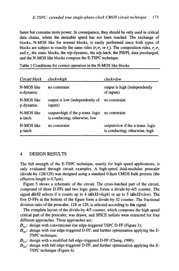
Figure 5 shows a schematic of the circuit. The cross-hatched part of the circuit, composed of three D-FFs and two logic gates, forms a divide-by-4/5 counter. The signal div32 selects if it counts up to 4 (div32=high) or up to 5 (div32=low). The five D-FFs at the bottom of the figure form a divide-by-32 counter. The fractional division ratio of the prescaler, 128 or 129, is selected according to Sm signal.
The complete layout of the divide-by-4/5 counter, which composes the high speed critical part of the prescaler, was drawn, and SPICE netlists were extracted for four different approaches. These approaches are: D01 : design with conventional rise edge-triggered TSPC D-FF (Figure 3); D0 ,: design with rise edge-triggered D-FF, and further optimisation applying theE
TSPC technique; D 0 J: design with a modified fall edge-triggered D-FF (Chang, 1996); D 04 : design with fall edge-triggered D-FF, and further optimisation applying theE
TSPC technique (Figure 6).
174 Part Five High Speed Circuit Techniques
----
Figure 5 Schematic of a dual modulus prescaler ( divide-by-128/129).
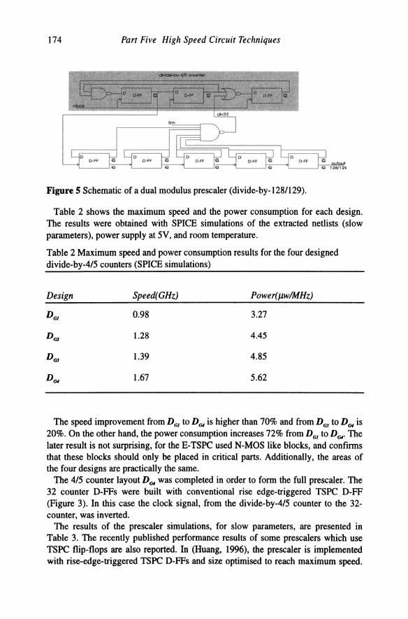
Table 2 shows the maximum speed and the power consumption for each design. The results were obtained with SPICE simulations of the extracted netlists (slow parameters), power supply at 5V, and room temperature.
Table 2 Maximum speed and power consumption results for the four designed divide-by-4/5 counters (SPICE simulations)
Design Speed(GHz) Power( J.LwiMHz)
DGI 0.98 3.27
DGZ 1.28 4.45
DGJ 1.39 4.85
DGI 1.67 5.62
The speed improvement from DG1 to DGI is higher than 70% and from DGJ to DGI is 20%. On the other hand, the power consumption increases 72% from DG1 to DGI. The later result is not surprising, for the E-TSPC used N-MOS like blocks, and confirms that these blocks should only be placed in critical parts. Additionally, the areas of the four designs are practically the same.
The 4/5 counter layout DGI was completed in order to form the full prescaler. The 32 counter D-FFs were built with conventional rise edge-triggered TSPC D-FF (Figure 3). In this case the clock signal, from the divide-by-4/5 counter to the 32-counter, was inverted.
The results of the prescaler simulations, for slow parameters, are presented in Table 3. The recently published performance results of some prescalers which use TSPC flip-flops are also reported. In (Huang, 1996), the prescaler is implemented with rise-edge-triggered TSPC D-FFs and size optimised to reach maximum speed.
E-TSPC: extended true single-phase-clock CMOS circuit technique 175
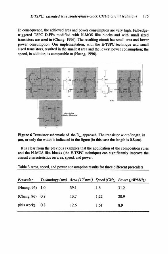
In consequence, the achieved area and power consumption are very high. Fall-edgetriggered TSPC D-FFs modified with N-MOS like blocks and with small sized transistors are used in (Chang, 1996). The resulting circuit has small area and lower power consumption. Our implementation, with the E-TSPC technique and small sized transistors, resulted in the smallest area and the lowest power consumption; the speed, in addition, is comparable to (Huang, 1996).
Figure 6 Transistor schematic of the 0 04 approach. The transistor width/length, in f.1m, or only the width is indicated in the figure (in this case the length is 0.8f.1m).
It is clear from the previous examples that the application of the composition rules and the N-MOS like blocks (the E-TSPC technique) can significantly improve the circuit characteristics on area, speed, and power.
Table 3 Area, speed, and power consumption results for three different prescalers
Prescaler Technology (J.Un) Area (10.1mm2) Speed (GHz) Power (J.LW/MHz)
(Huang, 96) 1.0
(Chang, 96) 0.8
(this work) 0.8
39.1
13.7
12.6
1.6 31.2
1.22 20.9
1.61 8.9
176 Part Five High Speed Circuit Techniques
5 CONCLUSIONS
The new Extended True Single-Phase-Clock (E-TSPC) CMOS circuit technique was presented and analysed. The E-TSPC technique represents an improvement in the following aspects: • the composition rules are little restrictive allowing the designer to take full
advantage of the blocks potential; • the N-MOS like blocks can increase the speed of the circuit everywhere it is
necessary. Moreover, since the conventional and N-MOS like blocks follow the same composition rules, they are exchangeable, and the cost of any substitution, in terms of time, is very small;
• p-data chains can be designed to be as fast as n-data chains. In fact, p-data chains can use only N-MOS like p-latches, which have the logic implemented with ntransistors.
Some design results show that speed increases and power/area savings are found with the E-TSPC technique application. A complete high-speed dual-modulus prescaler ( divide-by-128/129) was designed in a 0.8~m CMOS process, and simulations of the extracted circuits from layout reached 1.6lGHz with power consumption of 8.9~W/MHz.
6 REFERENCES
Afghahi, M. and Svensson, C. (1990) A unified single-phase clocking schema for VLSI systems. IEEE J. Solid-State Circuits, vol.25, 225-35.
Chang, B et al. (1996) A 1.2 GHz CMOS dual-modulus prescaler using new dynamic D-type flip-flops. IEEE J. Solid-State Circuits, vol.31, 749-52.
Goncalves, N.F. et al. (1983) NORA: a racefree dynamic CMOS technique for pipelined logic structures. IEEE J. Solid-State Circuits, vol.l8, 261-6.
Goncalves, N.F. (1984) NORA: a racefree CMOS technique for register transfer systems. Ph.D. Thesis, Katholieke Universiteit Leuven, Leuven, Belgium.
Huang, Q. et al. (1996) Speed optimization of edge-triggered CMOS circuits for gigahertz single-phase clocks. IEEE J. Solid-State Circuits, vol.31, 456-65.
Krambeck, R.H. et al. (1982) High-speed compact circuits with CMOS, IEEE J. Solid-State Circuits, vol.l7, 614-9.
Weste, N.H.E. and Eshraghian, K. (1985) Principles of CMOS VLSI design, Addilson-Wesley Publishing Company, I" ed.
Yuan, J.-R. et al. (1987) A true single-phase-clock dynamic CMOS circuit technique. IEEE J. Solid-State Circuits, vol. 22, 899-901.
Yuan, J.-R. et al. (1993) New domino logic precharged by clock and data. Electronics Letters, vol.29, 2188-9.


![Materials Technology for Environmentally Green Micro ...lsi.usp.br/~acseabra/grad/2613_files/[4] Materials Technology for... · Materials Technology for Environmentally Green](https://img.pdfslide.us/doc/110x75/5b14f03d7f8b9a294c8cdbae/materials-technology-for-environmentally-green-micro-lsiuspbracseabragrad2613files4.jpg)


![TSPC Logic - Engineering · Domino, however, is a noninverting circuit, prohibiting some log-ical functions [4]. ... TSPC logic also affords designs having lower phase noise. With](https://img.pdfslide.us/doc/110x75/5aeb92f17f8b9a66258d8b39/tspc-logic-however-is-a-noninverting-circuit-prohibiting-some-log-ical-functions.jpg)