Embed Size (px)
Citation preview

©2013
Matthew Frank Parkinson
ALL RIGHTS RESERVED
ARCHITECTURAL INFLUENCE OF FEF2 FILMS ON ELECTROCHEMICAL
FAILURE MODES
By
MATTHEW FRANK PARKINSON
A Dissertation submitted to the
Graduate School-New Brunswick
Rutgers, The State University of New Jersey
in partial fulfillment of the requirements
for the degree of
Doctor of Philosophy
Graduate Program in Materials Science and Engineering
Written under the direction of
Professor GLENN G. AMATUCCI
And approved by
________________________
________________________
________________________
________________________
New Brunswick, New Jersey
May, 2013
ii
ABSTRACT OF THE DISSERTATION
ARCHITECTURAL INFLUENCE OF FEF2 FILMS ON ELECTROCHEMICAL FAILURE
MODES
By MATTHEW FRANK PARKINSON
Dissertation Director:
Glenn G. Amatucci
Iron fluoride (FeF2) is an attractive material for use as nanocomposite conversion
reaction based cathodes in lithium ion batteries because of its high specific theoretical
capacity of 571mAh/g. However, despite the optimistic potential of FeF2 to advance
battery cathodes, the cycling performance of the material requires further development
for it to be a viable cathode candidate. A deeper understanding is required of how
orientation, selective reaction fronts, and morphology impact the electrochemical
performance. FeF2 films of various degrees of vertical porosity and thickness were
fabricated through the use of dynamic glancing angle deposition. Respectable
performance was obtained with film thicknesses of 850nm, well above the
nanodimensions typically required to trigger electrochemical activity. The structure –
electrochemical property relationships were used to formulate insights on the electronic
and ionic transport limitations seen in typical nanocomposite powders.

iii
Dedication
This thesis is dedicated to the many that have provided me with support,
inspiration, encouragement and love throughout my lifetime.
I believe there are no rewards without sacrifice and this dissertation was no
exception. My wife Ashley is a wonderful human being that has supported my
education in endless ways despite the short term sacrifices it has required from our
relationship. I am grateful for her love and support. I am confident this education will
make our family stronger as we move forward with our future filled with new opportunity,
new priorities and happiness.
I would not have been able to achieve this dissertation with the support of my
parents, two sisters, extended family and friends. I am blessed to have two inspirational
parents who have lead me to success through passing their own unique life guiding
principles along to me. My two elder sisters have supported me in many ways through
my life including being my early academic tutors. I am grateful for my family’s support
and love.
Finally, I would like to acknowledge some of my early teachers who were
inspirational and encouraging; Don Crockett one of my science teachers at Novi High
School and the amazing engineering professors at Michigan Technological University.
These teachers were largely responsible for igniting my passion for science and
engineering.

iv
Acknowledgements
I would like to thank the Material Science and Engineering Department for the
opportunity to pursue my educational aspirations. Most importantly, I would like to thank
my advisor Professor Glenn Amatucci for welcoming a mechanical engineer into his
highly regarded energy storage research group (ESRG) and being patient with my
scientific development. Professor Amatucci is an extremely dedicated scientist and
professor. His endless commitment and passion for his research field sets an inspiring
example for the road map to achievement. I would like to thank the graduate program
director and committee member Professor Lisa Klein for the opportunity to join the
department and her dedication to my education. I would like to thank my committee
member Professor Ahmad Safari and the other Professors that have taught the
coursework with excellence. In addition, I would like to thank Professor Kimberly Cook-
Chennault for being on my committee.
There are many energy storage research group (ESRG) team members that
without their support this thesis in its form would not have been possible. I would like to
especially thank my fellow graduate student Jonthan Ko for his support with lab
activities. In addition, I would like to thank the highly talented and always eager to assist
engineers Barry Vaning and John Gural. Barry and John have contributed many
innovated ideas supporting the design and development of the custom ebeam
deposition chamber which was the foundation of this thesis. I would like to thank past
student Dr. Andrew Gmitter for his willingness to assist me in the lab whenever it I
needed his support. I would like to thank Sheel Sanghvi for his support with XRD and
depositing the LiPON coating to the electrodes. In addition, I would like to thank the

v
following past and present members; Kimberly Scott, James Kantor, Dr. William Yourey,
Anthony Ferrer, Josh Kim, Dr. Wei Tong, Dr. Nathalie Pereira, Anna Halajko, Fadwa
Badway, Irene Plitz, and Linda Sung.
I acknowledge the U.S. Government and the Northeastern Center for Chemical Energy
Storage (NECCES), an Energy Frontier Research Center funded by the U.S.
Department of Energy, Office of Science, Office of Basic Energy Sciences under Award
Number DE-SC0001294, for their financial support.
vi
Table of Contents
ABSTRACT OF THE DISSERTATION ........................................................................... ii
Dedication ..................................................................................................................... iii
Acknowledgements ..................................................................................................... iv
Table of Contents ......................................................................................................... vi
List of Figures ........................................................................................................... viii
List of Tables .............................................................................................................. xiv
1. Introduction .............................................................................................................. 1
1.1. Introduction to Lithium Batteries .......................................................................... 1
1.1.1. General Lithium Cell Overview and Terminology ....................................... 1
1.1.2. Lithium Cell Cathode Materials ................................................................. 3
1.1.3. Thin Film Batteries Brief Review ............................................................. 11
1.1.4. Metal Fluoride Thin Film Electrodes ....................................................... 13
1.1.5. Iron Fluoride (FeF2) Thin Films ............................................................... 17
1.1.6. 3D Nanostructured Electrodes ................................................................ 18
2. Electrochemical Impedance Spectroscopy (EIS) ................................................ 21
2.1. Theory ............................................................................................................... 21
2.1.1. Double Layer Capacitance ....................................................................... 21
2.1.2. Randles Impedance Nyquist Plot and AC Impedance Equivalent Circuit 23
2.1.3. Constant Phase Element (CPE) .............................................................. 26
2.2. Practical Applications ........................................................................................ 30
2.2.1. Charge Transfer Impedance and Diffusion ............................................ 30
2.2.2. Electrolyte Accessible Surface Area ........................................................ 33
3. Physical Vapor Deposition (PVD) Thin Films ...................................................... 35
3.1.Introduction ....................................................................................................... 35
3.2.Vacuum Pumps ................................................................................................. 36
3.3.Vacuum Measurement ...................................................................................... 39
3.4.Physical Vapor Deposition Processing ............................................................. 40
3.4.1. Source Vaporization Techniques ............................................................. 41
3.4.2. Vapor Flux Transport ............................................................................... 45
3.4.3. Film Nucleation and Growth .................................................................... 46
3.4.4. Glancing Angle Deposition (GLAD) ...................................................................... 50

vii
4. Experimental Techniques ..................................................................................... 54
4.1. Preparation of the Thin Film Substrate and Current Collector ........................... 54
4.2. Programming of the Dynamic Substrate Drum System ..................................... 55
4.3. X-Ray Diffraction (XRD) .................................................................................... 57
4.4. Stylist Profilometer Thin Film Thickness Measurement ..................................... 61
4.5. Field Emission Scanning Electron Microscope (FESEM) .................................. 64
4.6. Electrochemical Characterization ..................................................................... 66
5. Design and Fabrication of a Custom E-beam Deposition System .................... 67
5.1. Project Background ........................................................................................... 67
5.2. Vacuum Chamber Preparation, Assembly and Testing ..................................... 69
5.3. Design of a Programmable Substrate Drum System ......................................... 75
5.4. Design of an Electron Beam Deposition System ............................................... 81
6. Effect of Vertically Structured Porosity on Electrochemical Performance of FeF2 Films ............................................................................................................. 93
6.1. Introduction ........................................................................................................ 93
6.2. Experimentation ................................................................................................ 97
6.3. Results ............................................................................................................ 101
6.4. Discussion ....................................................................................................... 123
6.5. Conclusion ....................................................................................................... 131
7. Effect of FeF2 Thin film Microstructure on Surface Specific Capacitance .... 132
7.1. Introduction ...................................................................................................... 132
7.2. Experimentation .............................................................................................. 138
7.3. Results ............................................................................................................ 141
7.4. Discussion ....................................................................................................... 154
7.5. Conclusion ....................................................................................................... 155
8. Future Work .......................................................................................................... 157
9. Summary .............................................................................................................. 158
10. References ........................................................................................................... 159
11. Curriculum vitae .................................................................................................. 165
viii
List of Figures
Figure 1.1: Schematic of a typical coin cell battery ......................................................... 2
Figure 1.2: Schematic of the inner workings of an insertion LIB ...................................... 5
Figure 1.3: Visual comparison of the three types of cathodes ......................................... 7
Figure 1.4: FeF2 rutile-type tetragonal structure showing the diffusion barrier contrast
between the (110) and (001) channel.............................................................................. 8
Figure 1.5: Thin film battery by Oak Ridge National Lab ............................................... 11
Figure 2.1: Ions from solution forming a double layer capacitance within a porous
electrode ....................................................................................................................... 23
Figure 2.2: Randles impedance Nyquist plot and equivalent AC circuit ........................ 24
Figure 2.3: Impedance plots for various shapes of pores .............................................. 26
Figure 2.4: CPE equivalent circuits, a) non-porous and b) porous electrodes ............... 28
Figure 2.5: Schematic of a pore with smooth walls and its represented Nyquist plot .... 29
Figure 2.6: Schematic of a pore which has porous walls and it’s represented Nyquist
plot. ............................................................................................................................... 30
Figure 2.7: Ideal conducting electrodes equivalent RC circuit and Nyquist plot ............ 31
Figure 2.8: Ideal polarizable electrodes equivalent RC circuit and Nyquist plot ............ 31
Figure 2.9: Nyquist plots of cells (a) balanced bulk and faradaic resistances, (b) more
highly conducting electrodes with relatively large bulk resistance, and (c) nearly blocking
electrodes with relatively small bulk resistance ............................................................. 33
Figure 2.10: Definition of pore type showing macro, meso and micro pores ................. 35
Figure 3.1: Cutaway view of a typical Cryo-Torr pump .................................................. 38
Figure 3.2: Effective pressure monitoring ranges of various vacuum gauges ............... 40
ix
Figure 3.3: Typical resistance heated thermal evaporation system ............................... 41
Figure 3.4: Typical pulse laser evaporation system ...................................................... 42
Figure 3.5: Typical glow discharge sputtering evaporation system ............................... 43
Figure 3.6: Typical electron beam evaporation system ................................................. 44
Figure 3.7: Comparison of short verse long mean free ................................................. 45
Figure 3.8: Cosine distribution of vapor particles leaving a point on the source ............ 46
Figure 3.9: Steps in film growth ..................................................................................... 48
Figure 3.10: Step #4 in Film Growth, Heterogeneous Nucleation ................................. 49
Figure 3.11: Typical glancing angle deposition apparatus ............................................. 51
Figure 3.12: Glancing angle shadow effect ................................................................... 52
Figure 3.13: Description of various GLAD ..................................................................... 53
Figure 4.1: Substrate holder showing attached Al-7075 strips and glass slide .............. 54
Figure 4.2: Typical manual hand press used to punch the substrate/film into discs ...... 55
Figure 4.3: Ormec servo motion controller assembly and wiring diagram ..................... 56
Figure 4.4: NaCl unit cell showing atomic planes .......................................................... 57
Figure 4.5: Definition of Bragg’s law .............................................................................. 59
Figure 4.6: Definition of diffraction peak intensity .......................................................... 59
Figure 4.7: X-ray diffractometer used for the majority of XRD experiments a Bruker D8
...................................................................................................................................... 61
Figure 4.8: Dektak 150 Profilometer used to measure film thickness and topography .. 63
x
Figure 4.9: Dektak 150 Profilometer3D topography mapping of a 58-62° FeF2 thin film
...................................................................................................................................... 64
Figure 4.10: A Zeiss ΣIGMA Field Emission SEM used in the experiments .................. 65
Figure 4.11: Solartron Models SI 1287 and SI 1260 used for EIS in the experiments ... 67
Figure 5.1: Previously used multiple chamber web coater ............................................ 68
Figure 5.2: Detailed planning schedule for the vacuum chamber development ............ 70
Figure 5.3: Completed ebeam deposition chamber valve switch panel ......................... 71
Figure 5.4: Removal and welding of the web coater chamber backing plate to create an
individual custom chamber ............................................................................................ 73
Figure 5.5: FEA simulation of chamber backing plate L-bracket support ...................... 74
Figure 5.6: 2D Fabrication drawings of the substrate drum system .............................. 75
Figure 5.7: Substrate drum positional resolution calculation ......................................... 77
Figure 5.8: Schematic of a ferrofluidic driveshaft .......................................................... 78
Figure 5.9: CAD showing the substrate drum in minimum height position .................... 79
Figure 5.10: CAD showing the substrate drum in its maximum height position with
185mm of total vertical adjustment ................................................................................ 79
Figure 5.11: Disassembly for drum geometry modifications .......................................... 80
Figure 5.12: Completed fabricated substrate drum system ........................................... 81
Figure 5.13: Picture of the completed ebeam deposition system ................................. 83
Figure 5.14: Results of a titanium deposition showing substrate thickness distribution ...
...................................................................................................................................... 86
Figure 5.15: View of chamber with the substrate drum rotated in GLAD position ......... 87
xi
Figure 5.16: Joule cross section polisher ..................................................................... 88
Figure 5.17: FESEM images of a titanium 55° GLAD film deposited with the substrate
held at a 55° angle relative to horizontal base of the ebeam ......................................... 89
Figure 5.18: XRD results confirming single phase synthesis of FeF2 thin film ............. 90
Figure 5.19: XRD results of FeF2 a.) without Ti adhesion layer and b.) with Ti layer ... 92
Figure 6.1: Lithited film structures (a) classical static film and (b) porous dynamic film 96
Figure 6.2: Schematic comparing static verse dynamic deposition ............................... 99
Figure 6.3: XRD results (a) dynamic angular films (b) 48-52° dynamic films and (c) static
films ............................................................................................................................. 103
Figure 6.4: FESEM images of Static 400nm (a) 2kX (b) 35kX, Static 700nm (c) 2kX (d)
35kX, and Static 850nm (e) 2kX (f) 35kX .................................................................... 105
Figure 6.5: FESEM images of 0.65rpm 28°-32°(a) 2kX (b) 35kX, 38°-42°(c) 2kX (d)
35kX, 48°-52°(e) 2kX (f) 35kX, 58°-62°(g) 2kX (h) 35kX and 68°-72°(i) 2kX (j) 35kX 107
Figure 6.6: FESEM images of 0.65rpm 48°-52° at 35kX (a) 400nm and (b) 850nm .... 108
Figure 6.7: FESEM images at 35kX of (a) 60°-80° at 6.5rpm (b) 40°-60° at 6.5rpm (c)
40°-80° at 6.5rpm (d) 40°-80° at 16.25rpm and (e) 40°-80° at 26rpm ........................ 110
Figure 6.8: Image processing of 0.65rpm at 35kX (a) 28°-32° (5.2%), (b) 38°-42° (8.2%),
(c) 48°-52° (19.9%), (d) 58°-62° (26.4%) and (e) 68°-72° (39.2%) .............................. 112
Figure 6.9: Image processing of static films at 2kX (a) 400nm (1.1%), (b) 700nm (1.9%)
and (c) 850nm (1.3%) .................................................................................................. 113
Figure 6.10: Plot of porosity and interfacial area dependence on dynamic deposition
angle ........................................................................................................................... 114
Figure 6.11: Dynamic rocking angular electrodes (a) specific capacity as a function of
cycle number and (b) 1st discharge specific capacity profile ....................................... 117
xii
Figure 6.12: Influence of dynamic deposition angle on perimeter surface area and
capacity ....................................................................................................................... 118
Figure 6.13: Static vs. Dynamic electrodes (a) specific capacity as a function of cycle
number (b) 1st discharge specific capacity profile ....................................................... 120
Figure 6.14: 400nm Static vs. Dynamic electrodes cycled galvanostatically between
4.50 V and 1.0V (a) static deposition (b) 48°-52° dynamic deposition ......................... 121
Figure 6.15: 700nm Static vs. Dynamic electrodes cycled galvanostatically between
4.50 V and 1.0V (a) static deposition (b) 48°-52° dynamic deposition ......................... 122
Figure 6.16: 850nm Static vs. Dynamic electrodes cycled galvanostatically between
4.50 V and 1.0V (a) static deposition (b) 48°-52° dynamic deposition ......................... 123
Figure 6.17: FESEM images of lithiated films Static 400nm (a) 2kX (b) 35kX and
Dynamic 48°-52° 400nm (c) 2kX (d) 35kX .................................................................. 126
Figure 6.18: Image processing of Dynamic 48°-52° 400nm films at 35kX magnification
(a) pre-lithiated and (b) lithiated .................................................................................. 126
Figure 6.19: Voltage vs. Capacity of Static 400nm (a) LiPON=50nm and (b)
LiPON=100nm ............................................................................................................. 128
Figure 6.20: Voltage vs. Capacity of 48°-52° 400nm (a) LiPON=50nm and (b)
LiPON=100nm ............................................................................................................. 129
Figure 6.21: Voltage vs. Capacity of 48°-52° 700nm (a) LiPON=50nm and (b)
LiPON=100nm ............................................................................................................. 130
Figure 6.22: LiPON cells Discharge Capacity vs. Cycle Number (a) Static 400nm (b)
48°-52° 400nm and (c) 48°-52° 700nm ....................................................................... 131
Figure 7.1: Ions from Solution forming a Double Layer Capacitance within Porous
Electrode ..................................................................................................................... 135

xiii
Figure 7.2: Randles Impedance Nyquist Plot and AC Impedance Equivalent Circuit . 136
Figure 7.3: XRD results of (a) dynamic (b) 48°-52° 400nm,700nm,850nm (c) Static
400nm, 700nm, 850nm and (d) Static 600nm, 800nm, 1500nm ................................. 142
Figure 7.4: FESEM images of Static 400nm (a) 2kX (b) 35kX, Static 600nm (c) 2kX (d)
35kX, and Static 700nm (e) 2kX (f) 35kX, Static 800nm (g) 2kX (h) 35kX, Static 850nm
(i) 2kX (j) 35kX and Static 1500nm (k) 2kX (l) 35kX .................................................... 143
Figure 7.5: FESEM images of 0.65rpm 28°-32°(a) 2kX (b) 35kX, 38°-42°(c) 2kX (d)
35kX, 48°-52°(e) 2kX (f) 35kX, 58°-62°(g) 2kX (h) 35kX and 68°-72°(i) 2kX (j) 35kX.
.................................................................................................................................... 144
Figure 7.6: Image processing of 2kX FESEM images of Static 400nm (a), Static 600nm
(b), Static 700nm (c), Static 800nm (d), Static 850nm (e) and Static 1500nm (f). ...... 145
Figure 7.7: Image processing of 0.65rpm (a) 28°-32° 35kX, (b) 38°-42° 35kX, (c) 48°-
52° 35kX, (d) 58°-62° 35kX and (e) 68°-72° 35kX ....................................................... 147
Figure 7.8: Plot of static films capacitance verse frequency ........................................ 149
Figure 7.9: Nyquist Plot of Static 400nm ..................................................................... 150
Figure 7.10: Plots of static films (a) CPE-T vs. film thickness, (b) interfacial area vs. film
thickness and (c) interfacial area vs. CPE-T ............................................................... 151
Figure 7.11: Plot of static films capacitance verse frequency ...................................... 152
Figure 7.12: Nyquist Plot of Dynamic 48-52deg 700nm .............................................. 153
Figure 7.13: Plot of dynamic films (a) CPE-T vs. deposition angle, (b) interfacial area vs.
deposition angle and (c) interfacial area vs. CPE-T .................................................... 154

xiv
List of Tables
Table 1: Conversion vs. intercalation comparison…………………………………………..6
Table 2: Summary of XRD Analysis………………………………………………………..104
1
1 Introduction
1.1 Introduction to Lithium Batteries
One of the most important rechargeable energy storage technologies is the
lithium ion battery (LIBs). Since early development at Exxon in the 1970’s,
lithium battery technology has been of interest due to the fact that l ithium is
the most electropositive (–3.04V versus standard hydrogen electrode) and is
the lightest metal (MW=6.94g/mol, and specific gravity 0.53g/cc).
Traditionally, LIBs are used for a variety of mobile equipment, including cell
phones, laptop computers, and tools. Most recently, LIBs are showing as
promising candidates of power sources to electrif y the transportation sector.1
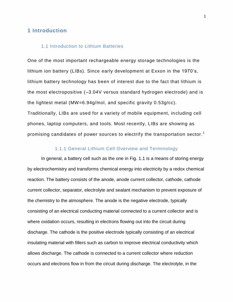
1.1.1 General Lithium Cell Overview and Terminology
In general, a battery cell such as the one in Fig. 1.1 is a means of storing energy
by electrochemistry and transforms chemical energy into electricity by a redox chemical
reaction. The battery consists of the anode, anode current collector, cathode, cathode
current collector, separator, electrolyte and sealant mechanism to prevent exposure of
the chemistry to the atmosphere. The anode is the negative electrode, typically
consisting of an electrical conducting material connected to a current collector and is
where oxidation occurs, resulting in electrons flowing out into the circuit during
discharge. The cathode is the positive electrode typically consisting of an electrical
insulating material with fillers such as carbon to improve electrical conductivity which
allows discharge. The cathode is connected to a current collector where reduction
occurs and electrons flow in from the circuit during discharge. The electrolyte, in the
2
form of an electrical insulating but ionic conducting liquid, gel or solid such as a
polymer, is the passageway to exchange ions (Li+) back and forth between the anode
and cathode. The separator, typically in the form of a porous polymer or paper, is an
electronically insulating material placed as a spacer between the positive and negative
electrodes necessary to prevent a short circuit condition. The separator can be
eliminated from the battery when an electrolyte of solid form with mechanical rigidity is
used which has sole capability of adding space between the electrodes to prevent a
short circuit.
Figure 1.1: Schematic of a typical coin cell battery
Multiple battery cells can be assembly together in a series or parallel circuit
arrangement to tailor the performance with a specific application. In applications that
require higher operating voltage or higher capacity, multiple cells are arranged in series
and parallel respectively.
There are two forms of battery cells, primary and secondary and their definition
depends on how they discharged. A primary battery cell is limited to a single discharge
due to the form of chemistry used in the cathode. Primary batteries can be found in
applications such as medical pacemakers, watches and flashlights. Some advantages

3
to primary batteries are reduced up front cost compared with secondary batteries which
make them ideal for single use applications and they have a relatively higher energy
density and longer shelf life because no design compromises are necessary to
accommodate recharging. Primary batteries are at a disadvantage due to the cost of
continuous replacement which adds to waste streams and they are not suited for high
load applications which would add to the frequency of replacement. Secondary
batteries which are commonly called rechargeable batteries because of their ability to
be charged to their initial energy condition by forcing current and ions in the direction
opposite that of discharge. Secondary batteries can be found in applications such as
power tools, laptops and hybrid vehicles. Some advantages to secondary batteries are
cost efficiency over the long term due replacing less frequently, higher power densities,
higher discharge rates under heavy loads and improved cold temperature performance.
The limitations of secondary batteries include higher up front cost, poorer charge
retention, lower energy density and special design considerations due to lithium’s
reactivity with oxygen.
1.1.2 Lithium Cell Cathode Materials
There are three known types of reaction mechanisms currently in LIBs,
intercalation, displacement and conversion. For all three mechanisms, lithium ion
chemistry moves electrons through an external circuit by insertion of Li+ into one
electrode material while extracting Li+ from the opposing electrode material. In
intercalation, the process is referred to as the “rocking chair” mechanism which is
another name for “Li-ion battery”.
4
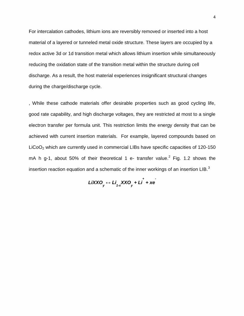
For intercalation cathodes, lithium ions are reversibly removed or inserted into a host
material of a layered or tunneled metal oxide structure. These layers are occupied by a
redox active 3d or 1d transition metal which allows lithium insertion while simultaneously
reducing the oxidation state of the transition metal within the structure during cell
discharge. As a result, the host material experiences insignificant structural changes
during the charge/discharge cycle.
, While these cathode materials offer desirable properties such as good cycling life,
good rate capability, and high discharge voltages, they are restricted at most to a single
electron transfer per formula unit. This restriction limits the energy density that can be
achieved with current insertion materials. For example, layered compounds based on
LiCoO2 which are currently used in commercial LIBs have specific capacities of 120-150
mA h g-1, about 50% of their theoretical 1 e- transfer value.2 Fig. 1.2 shows the
insertion reaction equation and a schematic of the inner workings of an insertion LIB.3
LiXXOy ↔ Li
1-xXXO
y + Li
+
+ xe-
5
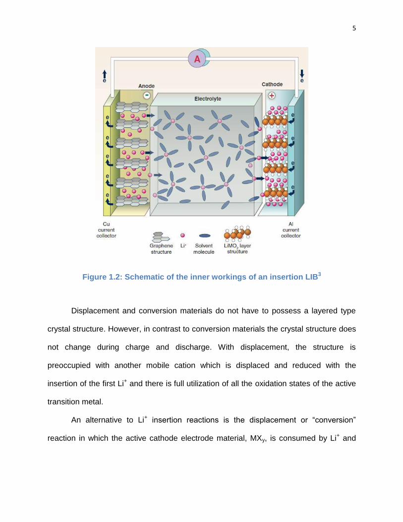
Figure 1.2: Schematic of the inner workings of an insertion LIB3
Displacement and conversion materials do not have to possess a layered type
crystal structure. However, in contrast to conversion materials the crystal structure does
not change during charge and discharge. With displacement, the structure is
preoccupied with another mobile cation which is displaced and reduced with the
insertion of the first Li+ and there is full utilization of all the oxidation states of the active
transition metal.
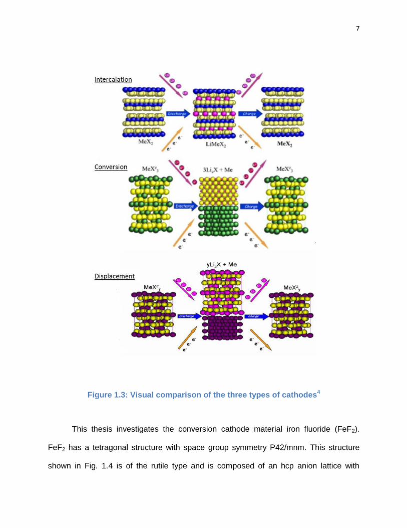
An alternative to Li+ insertion reactions is the displacement or “conversion”
reaction in which the active cathode electrode material, MXy, is consumed by Li+ and
6
reduced to the metal, M0, and a corresponding lithium compound, Liz/yX and oxidation of
these should return the material to its initial state.
nyLi+ + MxXy + nye− ↔ yLinX + xM
In the conversion reaction equation above, the metal cation is represented by M
and the anion by X. A large theoretical energy density is possible because this reaction
can make use of all energetically favorable valence states of the metal cation. Although,
reversible conversion reactions have been demonstrated with a variety of materials
including metal oxides, metal nitrides, metal sulfides, and metal fluorides, only metal
fluorides have a high enough potential to be used as Li-ion cathodes.4 This is due to the
fact that the conversion reaction potential is directly proportional to the strength of the
ionic bond. Despite metal fluorides high energy density they are limited by their wide
band gap corresponding in electronically insulating behavior which has inhibited the use
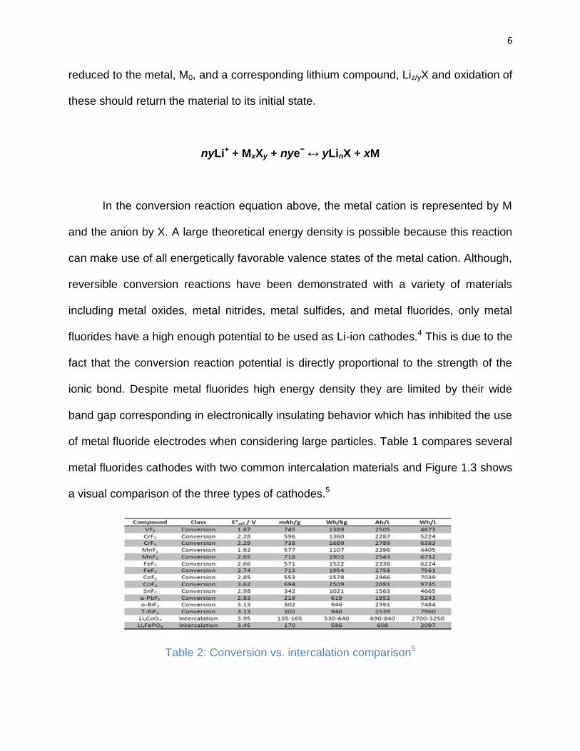
of metal fluoride electrodes when considering large particles. Table 1 compares several
metal fluorides cathodes with two common intercalation materials and Figure 1.3 shows
a visual comparison of the three types of cathodes.5
Table 2: Conversion vs. intercalation comparison5
7
Figure 1.3: Visual comparison of the three types of cathodes4
This thesis investigates the conversion cathode material iron fluoride (FeF2).
FeF2 has a tetragonal structure with space group symmetry P42/mnm. This structure
shown in Fig. 1.4 is of the rutile type and is composed of an hcp anion lattice with
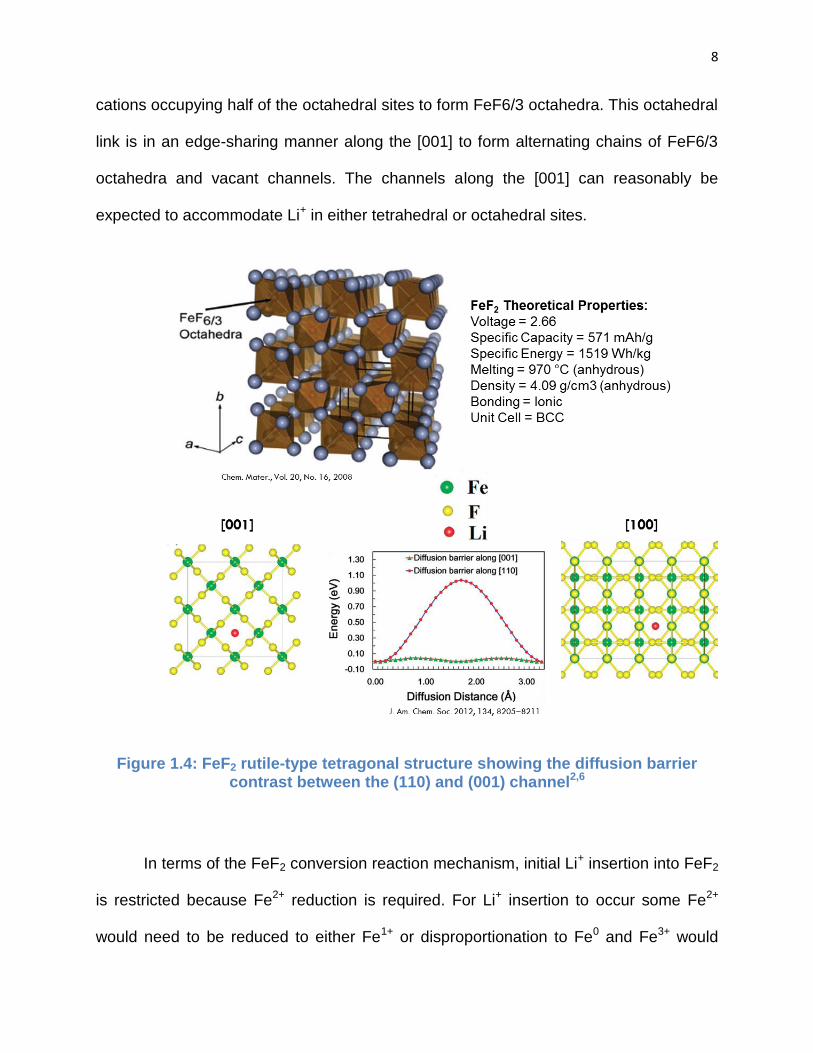
8
cations occupying half of the octahedral sites to form FeF6/3 octahedra. This octahedral
link is in an edge-sharing manner along the [001] to form alternating chains of FeF6/3
octahedra and vacant channels. The channels along the [001] can reasonably be
expected to accommodate Li+ in either tetrahedral or octahedral sites.
Figure 1.4: FeF2 rutile-type tetragonal structure showing the diffusion barrier contrast between the (110) and (001) channel2,6
In terms of the FeF2 conversion reaction mechanism, initial Li+ insertion into FeF2
is restricted because Fe2+ reduction is required. For Li+ insertion to occur some Fe2+
would need to be reduced to either Fe1+ or disproportionation to Fe0 and Fe3+ would
9
need to take place. In general, solid-state Fe1+ is very unlikely and oxidation states <2+
are uncommon for elements of the first transition series. If some Fe2+ reduction to Fe0
combines with some Fe2+ oxidation to Fe3+, then metallic iron would likely precipitate out
of the iron fluoride structure.7 In this case, the mechanism would not be a strict insertion
reaction because it requires an exchange of iron with lithium. During this process it
would be possible for Li+ to either fill an interstitial site in the channels, occupy the site
that Fe0 is removed from, or occupy space that is a combination of both limits. Another
possibility exists in which two Li+ exchange for one Fe2+ of the rutile structure. There are
many possibilities in which the FeF2 structure can be altered during the conversion
reaction. One of the goals of this thesis is to discover new knowledge to better
understand this reaction mechanism.
Despite metal fluorides representing a route for high energy density positive
electrodes, they are limited by their wide band gap corresponding in electronically
insulating behavior and very poor ionic diffusion through the conversion front. The band
gap and electrical properties of FeF2 have been recently studied by YANG Zhen-hua et
al 2012.8 For their study, generalized gradient approximation calculations and the
Hubbard parameter method described the band gap as 2.565 eV. It was concluded that
the bond between Fe and F atoms in FeF2 is a mixture of ionic bond and covalent bond.
Another study, Santos-Ortiz et al 2013, provided insight into understanding of the band
structure of FeF2.9 Their study used UV-Vis-NIR spectrophotometer,
Photoluminescence (PL) and photoluminescence excitation (PLE) characterization. The
results indicated that FeF2 is a direct bandgap, n-type semiconductor, the Hall
coefficients were negative, electron mobility was 0.33cm2/V.s and resistivity was 0.255
10
>Ω.cm and the band structure was 3.4 eV with a workfunction of ~4.51- 4.66 eV. Based
on this band gap information, the study provided a guide for the selection of battery
application current collectors (i.e., Ohmic contacts). They concluded that stable, low
workfunction metals such as Al (Φ=4.19 eV), Ga (Φ=4.25 eV) or In (Φ=4.1 eV) could
provide Ohmic contacts to FeF2 films and are well suited for use as current collectors.
Due to the fact that FeF2 is a high bandgap insulator, transport is limited with
thick dense electrodes and the conversion reaction must proceed at the point of
electron transfer typically near the current collector. However, it has been show that
transport in powder FeF2 electrodes is greatly enhanced by the use of carbon or mixed
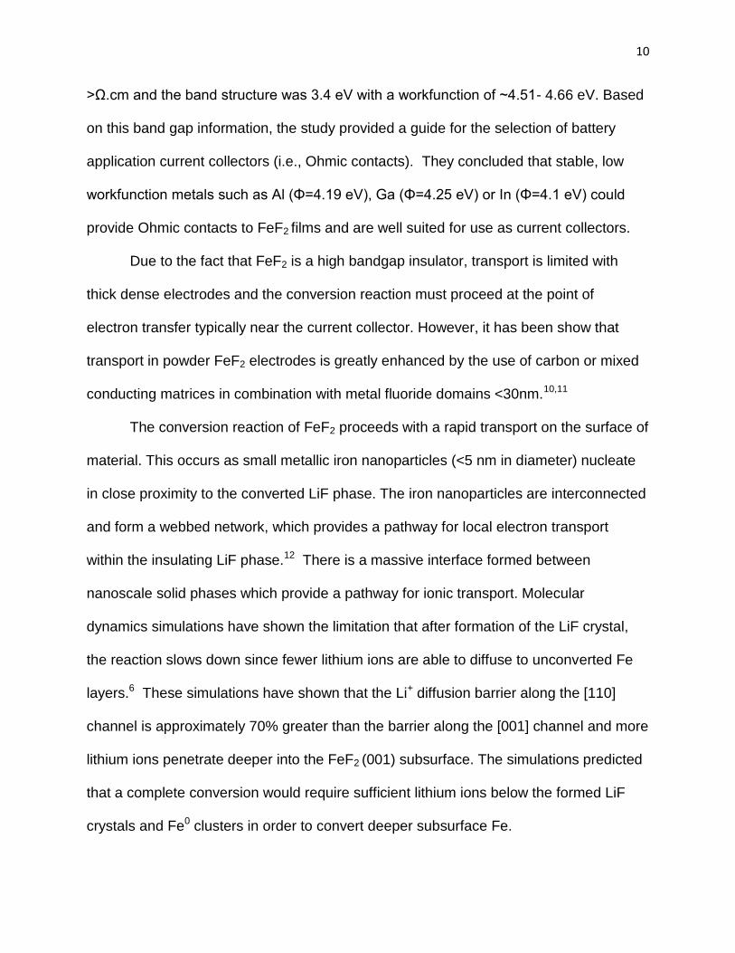
conducting matrices in combination with metal fluoride domains <30nm.10,11
The conversion reaction of FeF2 proceeds with a rapid transport on the surface of
material. This occurs as small metallic iron nanoparticles (<5 nm in diameter) nucleate
in close proximity to the converted LiF phase. The iron nanoparticles are interconnected
and form a webbed network, which provides a pathway for local electron transport
within the insulating LiF phase.12 There is a massive interface formed between
nanoscale solid phases which provide a pathway for ionic transport. Molecular
dynamics simulations have shown the limitation that after formation of the LiF crystal,
the reaction slows down since fewer lithium ions are able to diffuse to unconverted Fe
layers.6 These simulations have shown that the Li+ diffusion barrier along the [110]
channel is approximately 70% greater than the barrier along the [001] channel and more
lithium ions penetrate deeper into the FeF2 (001) subsurface. The simulations predicted
that a complete conversion would require sufficient lithium ions below the formed LiF
crystals and Fe0 clusters in order to convert deeper subsurface Fe.
11
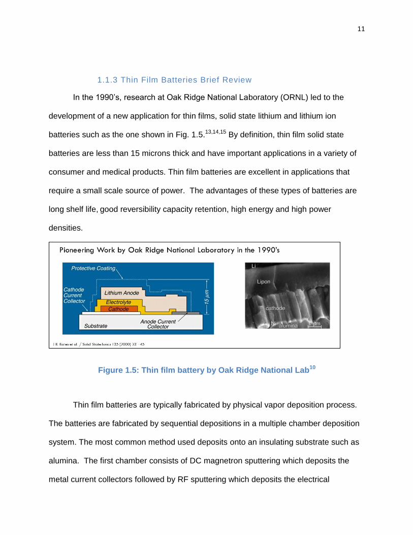
1.1.3 Thin Film Batteries Brief Review
In the 1990’s, research at Oak Ridge National Laboratory (ORNL) led to the
development of a new application for thin films, solid state lithium and lithium ion
batteries such as the one shown in Fig. 1.5.13,14,15 By definition, thin film solid state
batteries are less than 15 microns thick and have important applications in a variety of
consumer and medical products. Thin film batteries are excellent in applications that
require a small scale source of power. The advantages of these types of batteries are
long shelf life, good reversibility capacity retention, high energy and high power
densities.
Figure 1.5: Thin film battery by Oak Ridge National Lab10
Thin film batteries are typically fabricated by physical vapor deposition process.
The batteries are fabricated by sequential depositions in a multiple chamber deposition
system. The most common method used deposits onto an insulating substrate such as
alumina. The first chamber consists of DC magnetron sputtering which deposits the
metal current collectors followed by RF sputtering which deposits the electrical
12
insulating cathode. Finally, the electrolyte is deposited by RF magnetron sputtering of a
Li3PO4 source in a nitrogen plasma to create lithium phosphorus oxynitride (LiPON) and
metallic lithium anode is deposited by thermal evaporation. In addition, there is a
protective layered coating of Ti and parylene C to seal the battery to avoid exposure to
the atmosphere.
Lithium Phosphorus Oxynitride (LiPON) is the thin film solid electrolyte invented
at Oak Ridge National Laboratory in the early 1990s.16 Today, LiPON continues to be
the most widely used solid electrolyte for thin film batteries. The inventor J. B. Bates had
previous knowledge of introducing nitrogen to sodium phosphate and sodium silicate
glasses to enhance the chemical and thermal stability of the material and thought the
application could be used with lithium glass. Bates found that only a small percentage of
nitrogen replaces the oxygen in the composition. However, this small percentage of
nitrogen has a substantial effect on the ion conductivity and electrochemical stability. A
nitrogen/oxygen ratio of 0.1 in LiPON is associated with an ionic conductivity that is
approximately 40 times higher than nitrogen free Li3PO4 but approximately 100 times
less than liquid electrolytes. Typically a 1μm thick thin film of LiPON free of pinholes
provides sufficient ion conductivity while maintaining an electrical insulating barrier
between electrodes.
In addition to fully assembled batteries, thin films have several advantages which
can be applied as useful research tools in characterizing the properties of lithium
intercalation and conversion compounds. As a research tool the potential advantages
of thin films include (i) allowing investigation of electrochemical properties of pure
phases being free of binders; (ii) better accommodation of the strain of lithium insertion
13
and removal which improves cycle life; (iii) investigation of new reactions not possible
with bulk materials; (iv) short path lengths for electronic transport (permitting operation
with low electronic conducting materials or at higher power); and (v) short path lengths
for Li+ transport (permitting operation with low Li+ conducting materials or at higher
power).
1.1.4 Metal Fluoride Thin Film Electrodes
From the theoretical thermodynamic calculations, metal fluoride electrodes show
high energy density potential and have been studied for battery applications since the
1960’s.17 Metal fluorides have much higher voltage and the theoretical energy density
from the conversion reaction of metal fluorides exceeds that for metal oxides and
sulfides. This is due to the high electronegativity of fluorine which allows high ionic bond
character with the metal. A vast array of metal fluoride materials have been studied for
electrode application primarily comprised of powder verse thin films.4 The following
proceeding paragraphs will make brief reference to a few of these notable chemistries.
One of the highest energy density metal fluoride cathode materials is CuF2. In
1976 thin film electrodes of CuF2 were first studied by Hunter and Kennedy.18 The
electrodes were fabricated using Pb metal as anode, PbF2 as electrolyte. The thin film
cells developed open circuit voltages from 0.61 to 0.70V, compared to 0.70V theoretical.
The current density at room temperature was >10 ~μA/cm2 and showed vast
improvement with elevated temperatures. For the room temperature cells, the cathode
utilization was typically 30-40% in contrast to powder based CuF2 electrodes at the time
which had approximately 25% and slight improvement with sintering. The poor
utilization of most metal fluorides is thought to be explained by their low electronic
14
conductivity due to their intrinsically high band gaps. The attempts to recharge both thin
film and powder electrodes in these studies were unsuccessful. Nearly three decades
would past with little research activity reported on CuF2 electrodes until 2005 when
Badway et al. reported >90% utilization of CuF2 powder electrodes at theoretical
voltages for the first time.19 This was the first time nano-sized CuF2 domains embedded
in a matrix of metal oxide or sulfide mixed conductors. CuF2 nano-domains improved
the electronic transport difficulties, increased the current capability by allowing fast
transport to the individual nano-grains. More recently in 2011, the electrochemical
reaction of lithium and CuF2 thin films fabricated by pulse laser deposition with a
thickness of 100nm onto to stainless steel substrates was investigated by Z. W. Fu et al.
for the first time.20 Cycling showed a reversible capacity of 544mAh/g in the potential
range of 1.0–4.0 V and the results confirmed an insertion process followed by a fully
conversion reaction to Cu and LiF in the lithium electrochemical reaction of CuF2 thin
film electrode. It was noted that there was a reversible insertion reaction above 2.8V
which could provide a capacity of about 125mAh/g, which is claimed CuF2 is a potential
cathode material for rechargeable lithium batteries.
In 2005, the electrochemical reaction of CoF2 thin films with Li was investigated
by Z. W. Fu et al. for the first time.21 Thin films of cobalt fluoride were prepared in a
fabricated by pulse laser deposition with a thickness of approximately 100nm onto to
stainless steel substrates and a thin film coating of LiPON solid electrolyte was
deposited on the surface of the CoF2 as a separator between CoF2 and liquid electrolyte
to avoid a solution of CoF2. It was discovered that if the cell consisted of the deposited
CoF2 thin film without LiPON, LiPF6 as electrolyte and metal Li as the anode, the
15
charge/discharge curves of the cell were not achieved because CoF2 would be
dissolved in electrolyte and the voltage potential dropped to 0V during the initial
discharge. The LiPON coated cells had a specific capacity during the first discharge of
595 mAh/g. The second discharge had a capacity of 252 mAh/g, indicating a large
capacity loss of 58%. It was noted that the reversible conversion reaction of LiF with Co
may involve in the decomposition and formation of CoF instead of CoF2. Overall, the
results demonstrated the formation of metallic cobalt and LiF after the initial discharge
and the reversibility of CoF2 with lithium.
In 2006, Makimura/ Tarascon et al. reported the electrochemical behavior of
lithium and iron fluoride (FeF2 and FeF3) thin film electrodes fabricated by pulse laser
deposition with a thickness of less than 150nm onto stainless steel substrates.22 In
addition, the influence of various deposition conditions such as the target FeF2 or FeF3
and the substrate temperature were considered. The cells had a large irreversible
capacity loss on the first discharge but good cycling life was observed up to 30 cycles.
However, the voltage capacity profiles obtained from the cycling from both of the iron
fluoride thin films verse previously reported carbon metal fluoride nanocomposites were
different.
Bismuth fluoride (BiF3) was first investigated as a primary battery electrode
material in 1978 in powder macro form.23 Recently, Gmitter et al. 2012 for the first time
utilized BiF3 thin film electrodes deposited by thermal evaporation and of thicknesses of
1000 nm onto glassy carbon substrates in a study to investigate the impact of the
electrolyte reactions on the surface and subsurface chemistry of the inorganic
conversion material.24
16
In 2007, the electrochemical reaction of NiF2 thin films with Li was investigated by
Z. W. Fu et al. for the first time.25 Previously, only Badway et al. reported the discharge
and charge curves of NiF2 prepared by high-energy milling.26 Nano-sized 180nm thick
NiF2 thin films were prepared by pulse laser deposition (PLD) method onto stainless
steel substrates. The discharge/charge behaviors of NiF2 thin films were examined with
the first discharge capacity of 650 mAh/g being more than the theoretical capacity 540
mAh/g and a 17% capacity loss on the second discharge. The NiF2 thin films exhibited
higher specific capacities and better cycle performance than the CoF2 thin films.
However, during the electrochemical conversion reaction mechanism with lithium upon
cycling produced an intermediate product Li2NiF4 was identified in the counterpart
process of NiF2.
In 2010, the electrochemical reaction of lithium and MnF2 thin films fabricated by
pulse laser deposition with a thickness of approximately 100nm onto to stainless steel
substrates was investigated by Z. W. Fu et al. for the first time.27 During the first 50
cycles the material displayed a discharge capacity of 350 mAh/g to 530 mAh/g. The low
polarization and high capacity of MnF2 thin films showed that the material shows
potential as a future rechargeable battery.
As a side notation, fluorides react with water forming HF, which causes
difficulties in the preparation of fluoride materials. In addition, the fluoride ion and the
hydroxyl anion are similar in size and there is potential substitution which occurs by a
mechanism of isomorphic substitution and an accumulation of oxygen ions in the lattice
of bulk fluoride samples leads to formation of the second phase (oxide or oxofluoride).
However, the replacement of the fluorine atom by the oxygen atom is
17
thermodynamically unfavorable and fluorides are generally stable in dry air (oxygen)
even on heating.28 While working with metal fluorides, it is important to be aware of the
hydrolysis sensitivity of the material to avoid sample contamination.
In 1937, Domange carried out extensive studies of the equilibrium constants of a
wide variety of metal and alkaline fluorides at various temperatures.29 His experiment
utilized a platinum tube holding the fluoride, through which was passed a very specific
regulated stream of water vapor and the composition of the vapor phase was
established by analysis. The results concluded that the susceptibility to hydrolysis of
some common metal fluorides was found to decrease in the following order: CuF2, FeF3,
AgF, FeF2, CrF3, ZnF2, NiF2, CoF2, CdF2, PbF2, MnF2, MgF2, CaF2, and BaF2.
1.1.5 Iron Fluoride (FeF2) Thin Films
Prior to studying iron fluoride thin films for battery electrodes, there have been
few reported applications of iron fluoride thin films in literature. The few previous
literature studies involved investigating magnetic properties of iron fluoride using thin
films.
In 1996, J. Nogues et al. studied iron fluoride thin films and discovered positive
unidirectional exchange anisotropy in antiferromagnetic (FeF2) and ferromagnetic (Fe)
bilayers cooled through the antiferromagnetic critical temperature TN in large magnetic
fields.30 The FeF2 films were grown by sequential e-beam evaporation with a thickness
of 90 nm and rate of 0.2 nm/s. The substrates consisting of MgO [100] were heated to
450°C for 15mins prior to deposition, then cooled to the FeF2 growth temperature 200 <
18
TS < 300°C. By following this procedure, the FeF2 grows epitaxially along the [110]
direction.
In 2001, Yamazaki et al. studied 2D magnetism in iron fluoride thin films to verify
the results of theoretical studies on 2D spin systems and to identify novel properties
intrinsic to lower dimensions.31 FeF2 films of nano scale thicknesses were deposited by
electron beam evaporation at a deposition rate of 0.3˚A/sec on single-crystal substrate
Al2O3 and MgO substrates held at a temperature of 300 < TS < 400°C.
1.1.6 3D Nanostructured Electrodes
Traditional dense thin film battery electrodes with 2D geometries need a large
footprint area to achieve large capacities. The mechanical integrity of the film decreases
with thickness from the expansion and contraction during cycling so producing thicker
electrodes to store more energy is not a feasible approach. In addition, when the
thickness is increased in dense 2D electrodes the interfacial surface area remains
constant this reduces the power density of the battery. In terms of increasing the rate
capacity (power), the conventional approach with dense electrodes has been to reduce
the particle size to a few nanometers. Due to the limiting accessible interfacial area
which limits the opportunity to improve performance, 2D battery designs tend to be
inefficient as they compromise between energy density and power density.
Discovering new approaches to improve battery performance has led to 3D
nanostructured materials with porous morphologies. Nanostructured materials as
battery electrodes are of increasing interest to develop lithium batteries with higher
energy density, higher rate capability, and improved cycling stability. Nanostructures are
beneficial as a result of their large interfacial surface area, short distance for mass and
19
charge transport and mechanical stress absorption from charge/discharge volume
changes. For cathode materials with high band gaps, nanostructures have the potential
to improve the problem of low electronic conductivity. Obtaining high power in any
electrode can be achieved with porosity which ensures a ready supply of ions from the
electrolyte. However, porosity can sacrifice volumetric capacity at the price of high rate
capacity. This can be avoided if the optimum pore size is selected such that volume of
the solid will be optimized.
Despite, the many benefits of nanostructures there are some potential
challenges. The greater interfacial areas render the potential to increase solubility of
electrode material in the electrolyte solution and increase unwanted side reactions that
occur on electrode surface. In addition, the more open and exposed the area of the
electrode the greater the chances of collecting impurities and contaminants within the
material.
These structures are relatively new to battery electrodes and were initiated
through studies by Nishizawa et al 1997 where it was demonstrated that nanotube
morphologies formed in the pores of porous alumina templates improved the capacity
retention and rate capabilities of LiMn2O4 during cycling.32 Then in 2000, the same
group consisting of Martin and coworkers completed more studies on nanostructured
LiMn2O4 cathodes and tin oxide anodes.33,34 This initial use of nanostructured battery
electrodes, inspired a vast amount of studies using template synthesis as a means of
producing nanotubes, nanowires, and nanorods for positive electrode and negative
battery electrode materials.35,36,37,38,39 Currently, there is focus on more commercial
processes to form nanostructures such as thin film vacuum deposition and laser
20
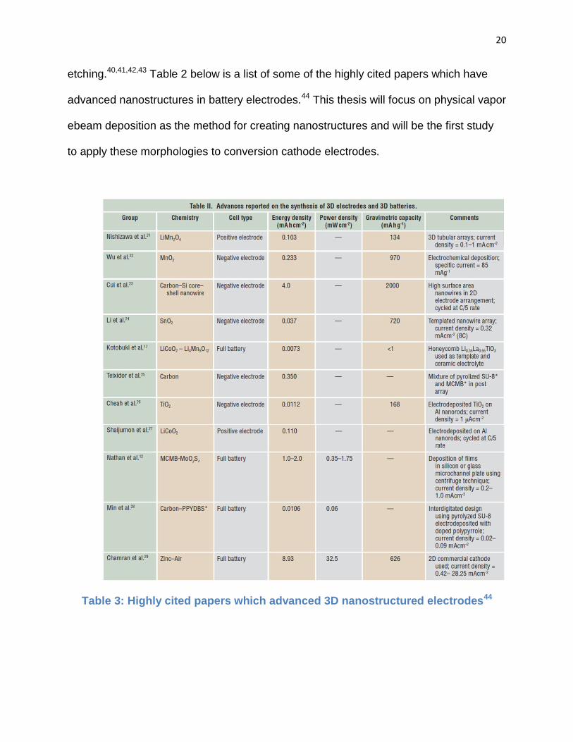
etching.40,41,42,43 Table 2 below is a list of some of the highly cited papers which have
advanced nanostructures in battery electrodes.44 This thesis will focus on physical vapor
ebeam deposition as the method for creating nanostructures and will be the first study
to apply these morphologies to conversion cathode electrodes.
Table 3: Highly cited papers which advanced 3D nanostructured electrodes44
21
2 Electrochemical Impedance Spectroscopy (EIS)
2.1 Theory
2.1.1 Double Layer Capacitance
Electrochemical impedance spectroscopy is capable of predicting the
electrochemical accessibility surface by measuring the double layer capacitance of the
electrode. Double layer capacitance was discovered by Helmholtz in 1879, Gouy in
1910, Chapman in 1913 and Stern in 1924 when they observed that ionic charges from
the electrolyte can be separated and forms a double layer across the surface of a
conductor (electrode). The double layer is established at the electrochemical interface
between the electrolyte and electrode where the charge transfer interfacial reaction
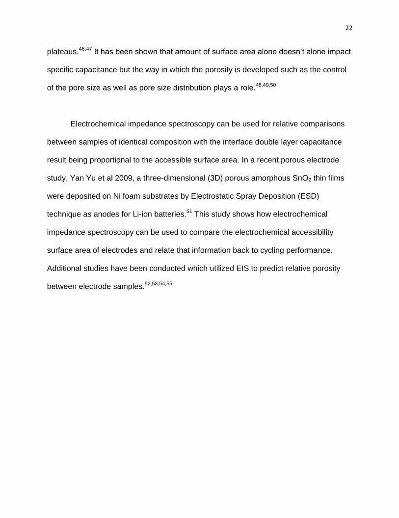
occurs as shown in Fig. 2.1.56 The capacitance of the double layer is proportional to the
electrochemical accessibility surface area of the electrode and inversely proportional to
the thickness of the double layer.
The double capacitance initially introduced by Helmholtz and then refined later by
Stern and Geary can be described according to C=ε A/d, where ε is the electrolyte
dielectric constant, A the surface area accessible to ions, and d the distance between
the A and center of the ion.
It is known that the surface area generally increases by the development of
porosity. However, O. Barbieri et al 2005 showed there is no simple linear relationship
between the surface area and the capacitance.45 It has been shown in several studies
using carbons that the specific capacitance has a linear dependence on surface area for
lower specific surface area, but as the surface area increases the relationship rapidly
22
plateaus.46,47 It has been shown that amount of surface area alone doesn’t alone impact
specific capacitance but the way in which the porosity is developed such as the control
of the pore size as well as pore size distribution plays a role.48,49,50
Electrochemical impedance spectroscopy can be used for relative comparisons
between samples of identical composition with the interface double layer capacitance
result being proportional to the accessible surface area. In a recent porous electrode
study, Yan Yu et al 2009, a three-dimensional (3D) porous amorphous SnO2 thin films
were deposited on Ni foam substrates by Electrostatic Spray Deposition (ESD)
technique as anodes for Li-ion batteries.51 This study shows how electrochemical
impedance spectroscopy can be used to compare the electrochemical accessibility
surface area of electrodes and relate that information back to cycling performance.
Additional studies have been conducted which utilized EIS to predict relative porosity
between electrode samples.52,53,54,55
23
Figure 2.1: Ions from solution forming a double layer capacitance within a porous electrode56
2.1.2 Randles Impedance Nyquist Plot and AC Impedance
Equivalent Circuit
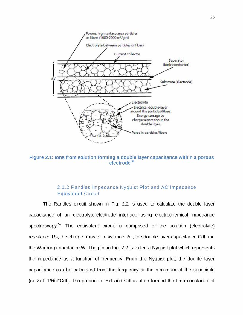
The Randles circuit shown in Fig. 2.2 is used to calculate the double layer
capacitance of an electrolyte-electrode interface using electrochemical impedance
spectroscopy.57 The equivalent circuit is comprised of the solution (electrolyte)
resistance Rs, the charge transfer resistance Rct, the double layer capacitance Cdl and
the Warburg impedance W. The plot in Fig. 2.2 is called a Nyquist plot which represents
the impedance as a function of frequency. From the Nyquist plot, the double layer
capacitance can be calculated from the frequency at the maximum of the semicircle
(ω=2πf=1/Rct*Cdl). The product of Rct and Cdl is often termed the time constant τ of
24
the electrochemical process. The 45° line indicating Warburg-limited behavior can be
extrapolated to the real axis. The intercept is equal to Rs + Rct – 2σCdl, from which σ
and diffusion coefficients can be calculated. The solution resistance, Rs, depends on
the ionic concentration, type of ions, temperature, and the geometry of the area in which
current is carried. The double-layer capacitance, Cdl, results from charge being stored
in the double layer at the electrolyte-electrode interface. The charge transfer resistance
Rct refers to current flow produced by redox reactions at the interface, and the Warburg
impedance results from the impedance of the current due to diffusion between the
electrolyte-electrode interface.
Figure 2.2: Randles impedance Nyquist plot and equivalent AC circuit57
The trend of a typical Nyquist plot for the Randles circuit can be explained. When
the oscillation frequency decreases, a very thin film of charge (double layer) starts to
grow on the electrode-electrolyte interface with time. With the formation of this film the
charge transfer resistance increases with a decrease of frequency. This eventually

25
increases impedance. In the low frequency region (to the right of the plot), the
accessible surface area becomes significant because large surface area allows more
charge to pass by and thus reduces impedance.
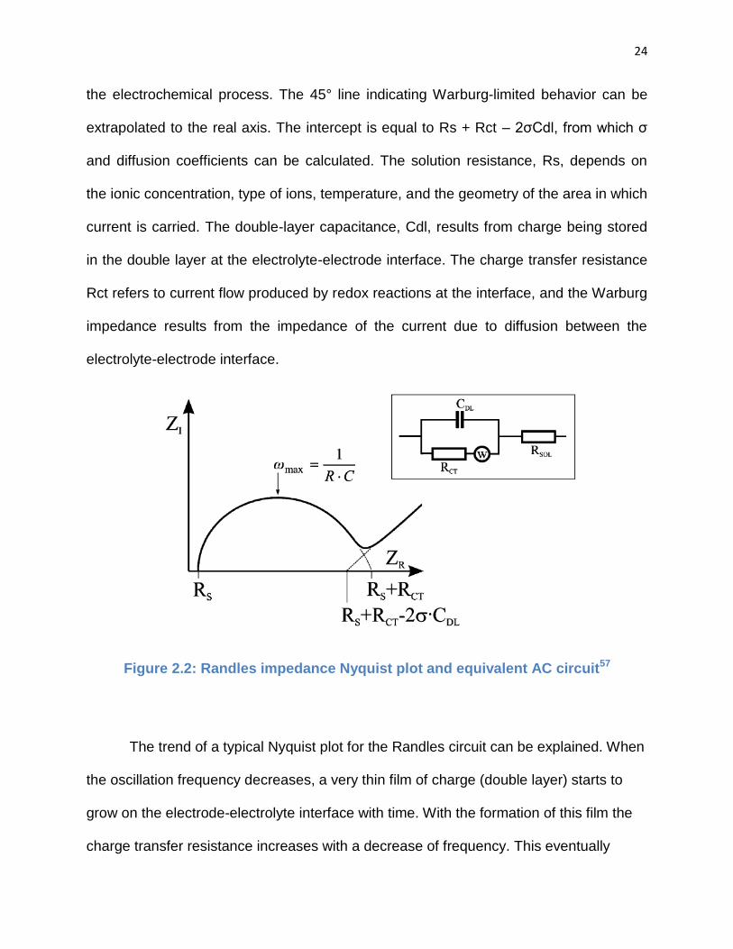
As an example to better understand the trend of the Nyquist plot as it relates to
the electrochemical accessibility surface area of a porous structure, simple models are
defined. In Fig, 2.3 a Nyquist plot showing the dependence of impedance with
frequency has been examined for various geometries of a single pore.58 This
comparison plot shows that the more sealed and less accessible the shape of a pore
the more the impedance exhibits a pseudo transfer resistance which is represented by a
semi-circle at high frequencies (to the left of the plot). Conversely, the more accessible
the shape of a pore the more linear the impedance curve.
26
Figure 2.3: Impedance plots for various shapes of pores58
2.1.3 Constant Phase Element (CPE)
Despite the classical circuit definitions previously discussed, the impedance results for
an electrode/electrolyte interface often reveal a frequency dispersion that cannot be
described by simple circuit elements such as resistances, capacitances, inductances or
convective diffusion (Warburg) impedance. The frequency dispersion is generally
attributed to a capacitance dispersion expressed instead in terms of a constant phase
element (CPE).59 Therefore, constant phase elements (CPE) are used extensively in
equivalent electrical circuits for fitting of experimental impedance data. In addition to be
associated with electrode porosity, the CPE behavior is influenced by distributed

27
surface reactivity, surface inhomogeneity, roughness or fractal geometry and to current
and voltage distributions associated with electrode geometry. The CPE consists of a
transmission line and an impedance given by Z = [Q (jw)α]-1, where j=√-1, Q is a
constant combining the resistance and capacitance properties of the electrode, and α
takes values between 0 and 1. However, this is only one definition for CPE and in the
literature different equations are proposed and depending on the formula used, the CPE
parameter is Q, 1/Q, or Qα and for capacitive dispersions the CPE exponent is α or (1 −
α) with α close to 1 or close to zero. As a flexible fitting parameter, the CPE has been
considered to represent a circuit parameter with limiting behavior as a capacitor for α =
1, a resistor for α = 0, and an inductor for α = −1. However, despite the fact that CPE is
an extremely flexible fitting parameter, the different expressions given for the CPE
underline that the physical meaning is still not clearly understood. Equivalent circuits for
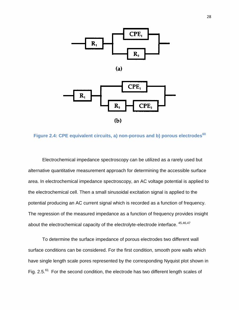
CPE are defined in Fig. 2.4 with a.) representing a non-porous flat electrode and b.)
representing a porous electrode. R1: resistance composed of solution resistance (Rs)
and electrode resistance (Re), R2: charge-transfer resistance across electrode/ solution
interface, CPE1: constant-phase element representing interfacial capacitance, CPE2:
pseudo capacitance of surface functional groups.60
28
Figure 2.4: CPE equivalent circuits, a) non-porous and b) porous electrodes60
Electrochemical impedance spectroscopy can be utilized as a rarely used but
alternative quantitative measurement approach for determining the accessible surface
area. In electrochemical impedance spectroscopy, an AC voltage potential is applied to
the electrochemical cell. Then a small sinusoidal excitation signal is applied to the
potential producing an AC current signal which is recorded as a function of frequency.
The regression of the measured impedance as a function of frequency provides insight
about the electrochemical capacity of the electrolyte-electrode interface. 45,46,47
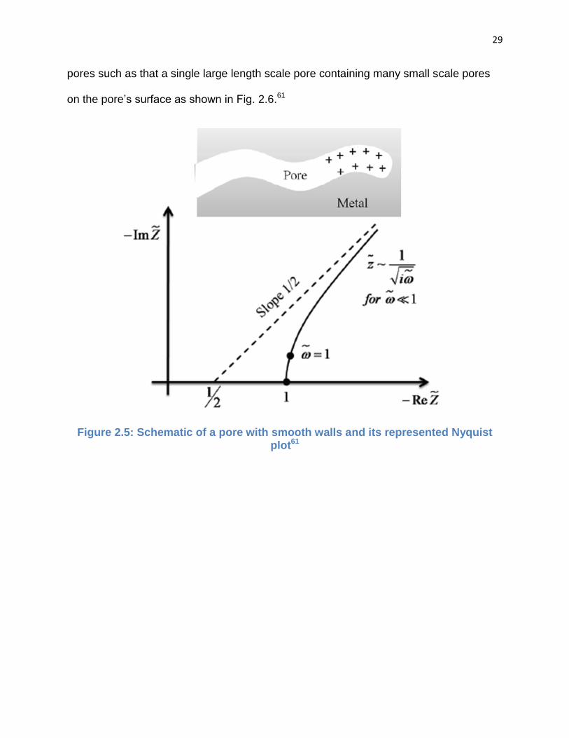
To determine the surface impedance of porous electrodes two different wall
surface conditions can be considered. For the first condition, smooth pore walls which
have single length scale pores represented by the corresponding Nyquist plot shown in
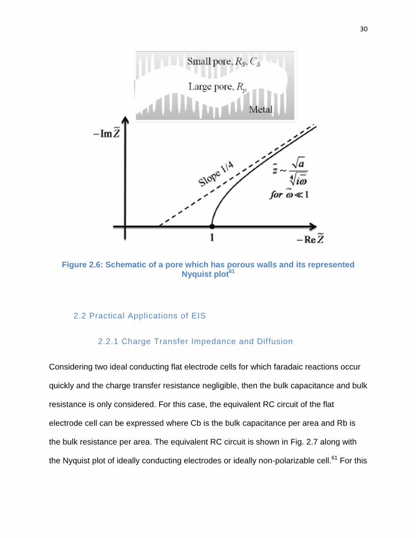
Fig. 2.5.61 For the second condition, the electrode has two different length scales of
29
pores such as that a single large length scale pore containing many small scale pores
on the pore’s surface as shown in Fig. 2.6.61
Figure 2.5: Schematic of a pore with smooth walls and its represented Nyquist plot61
30
Figure 2.6: Schematic of a pore which has porous walls and its represented Nyquist plot61
2.2 Practical Applications of EIS
2.2.1 Charge Transfer Impedance and Diffusion
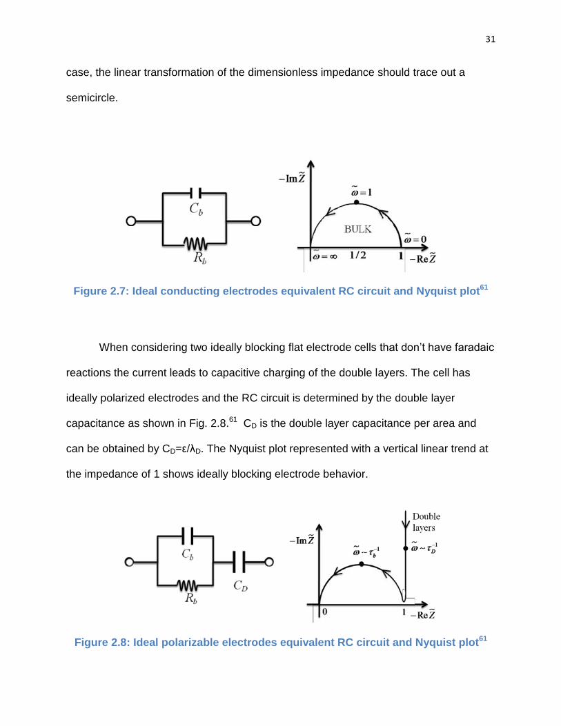
Considering two ideal conducting flat electrode cells for which faradaic reactions occur
quickly and the charge transfer resistance negligible, then the bulk capacitance and bulk
resistance is only considered. For this case, the equivalent RC circuit of the flat
electrode cell can be expressed where Cb is the bulk capacitance per area and Rb is
the bulk resistance per area. The equivalent RC circuit is shown in Fig. 2.7 along with
the Nyquist plot of ideally conducting electrodes or ideally non-polarizable cell.61 For this
31
case, the linear transformation of the dimensionless impedance should trace out a
semicircle.
Figure 2.7: Ideal conducting electrodes equivalent RC circuit and Nyquist plot61
When considering two ideally blocking flat electrode cells that don’t have faradaic
reactions the current leads to capacitive charging of the double layers. The cell has
ideally polarized electrodes and the RC circuit is determined by the double layer
capacitance as shown in Fig. 2.8.61 CD is the double layer capacitance per area and
can be obtained by CD=ε/λD. The Nyquist plot represented with a vertical linear trend at
the impedance of 1 shows ideally blocking electrode behavior.
Figure 2.8: Ideal polarizable electrodes equivalent RC circuit and Nyquist plot61
32
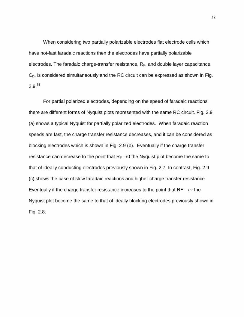
When considering two partially polarizable electrodes flat electrode cells which
have not-fast faradaic reactions then the electrodes have partially polarizable
electrodes. The faradaic charge-transfer resistance, RF, and double layer capacitance,
CD, is considered simultaneously and the RC circuit can be expressed as shown in Fig.
2.9.61
For partial polarized electrodes, depending on the speed of faradaic reactions
there are different forms of Nyquist plots represented with the same RC circuit. Fig. 2.9
(a) shows a typical Nyquist for partially polarized electrodes. When faradaic reaction
speeds are fast, the charge transfer resistance decreases, and it can be considered as
blocking electrodes which is shown in Fig. 2.9 (b). Eventually if the charge transfer
resistance can decrease to the point that RF →0 the Nyquist plot become the same to
that of ideally conducting electrodes previously shown in Fig. 2.7. In contrast, Fig. 2.9
(c) shows the case of slow faradaic reactions and higher charge transfer resistance.
Eventually if the charge transfer resistance increases to the point that RF →∞ the
Nyquist plot become the same to that of ideally blocking electrodes previously shown in
Fig. 2.8.
33
Figure 2.9: Nyquist plots of cells (a) balanced bulk and faradaic resistances, (b) more highly conducting electrodes with relatively large bulk resistance, and (c)
nearly blocking electrodes with relatively small bulk resistance61
2.2.2 Electrolyte Accessible Surface Area
Rate performance of a battery improves when there is a large contact surface
area between the electrode and the electrolyte. The contact surface area increases as
the electrode becomes more porous to the onset of micro porosity at 2nm at which
electrolyte molecules cannot easily enter. With increasing electrolyte accessible porosity
and this surface area of the electrode, the kinetics of mass transfer of Li ion is
increased.56,62
Typically the bulk mass transfer becomes more difficult as discharge continues
from the result of the cathode volume expansion during discharge and temporary or
permanent depletion of the vacancies near the surface of the primary particle depending
34
on the reaction mechanism. During the cathode volume expansion, the pores with fine
openings are easily sealed. As a result, mass transfer in and out of these pores
becomes more difficult. Designing an electrode that maintains large internal surface
area and allows for fast mass transfer to access this area is the key one of the keys to
achieving high rate capability.
Due to the aforementioned steric limitations, electrochemically accessible surface
area is normally smaller than the common BET measurement method of surface area.
Therefore, in designing an electrode for increased internal surface area it is important to
note that the porosity of the electrode is inversely related to the size of the particles
which comprise the electrode. For example, if the electrodes are produced from powder
the primary particles sinter together due to surface forces to form secondary particles.
Pores are formed in between the sintered secondary particles. The pore size depends
on the size and shape of primary particles and the conditions in which they are packed.
Pores with different sizes have different time constants and cannot be accessed at the
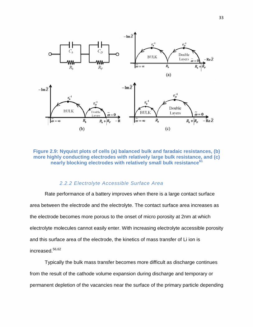
same time. By definition, there are three types of pores Macro (>50nm), Meso
(2<size<50nm) and Micro (<2nm) shown in Fig. 2.10.56 In addition, not all the pores can
be accessed electrochemically due to steric limitations relative to the size of the
electrolyte species.
35
Figure 2.10: Definition of pore type showing macro, meso and micro pores56
3 Physical Vapor Deposition (PVD) Thin Films
3.1 Introduction
Vacuum and thin film technology has an interesting history. The technology
arguably started with the invention of the first piston type vacuum pump in 1640 by Otto
van Guericke which was used to pump water out of mines. Vacuum science started to
evolve thereafter with various vacuum and pressure devices being invented. By 1800,
the invention of the voltaic battery by A. Volta led to the rapid development of vacuum
science involving electrical arcs. Faraday is credited for producing the first thin film
deposition in 1857 in which he used a Lyden battery to produce an arc which vaporized
a material for an optical property study. Ever since, vacuum and thin film technology
has continued to rapidly evolve and contribute greatly to society.
In the more recent past, thin film vacuum deposition has increasingly changed
everyday life with the influence it has in a large number of applications. Thin film
vacuum deposition applications are broad and include, but are not limited to; wear
36
resistance in medical orthopedic implants, reflection of IR light in low emissivity
architectural windows, flexible semiconductors for solar cell roof tiles, decorative
corrosion resistant coatings for plumbing fixtures and integrated circuits for computers
and electronic devices.
Thin film vacuum deposition starts with the selection of vacuum pressure that
meets the requirements of the specific process. The level of vacuum pressure selected
will depend on the materials being deposited and process equipment being utilized.
Overall, the use of vacuum and clean practices when depositing films minimizes
impurities to tolerable levels. The tolerable level of impurities depends on the material
being deposited and the chemical reactivity it has to the impurities. In addition, a
suitable vacuum level for the technology of equipment utilized needs to be considered.
There is a vast selection of vacuum pumps, pressure monitoring gauges and material
vaporization equipment in which to choose from. However, regardless of the equipment
selected, the overall transport of the vaporized material and growth of the thin film is
fundamentally the same.
3.2 Vacuum Pumps
Thin film vacuum deposition starts with the selection of vacuum pressure that
meets the requirements of the specific process. The level of vacuum pressure selected
will depend on the materials being deposited and process equipment being utilized.
Overall, the use of vacuum and clean practices when depositing films minimizes
impurities to tolerable levels. The tolerable level of impurities depends on the material
being deposited and the chemical reactivity it has to the impurities. In addition, a
suitable vacuum level for the technology of equipment utilized needs to be considered.
37
There is a vast selection of vacuum pumps, pressure monitoring gauges and material
vaporization equipment in which to choose from. However, regardless of the equipment
selected, the overall transport of the vaporized material and growth of the thin film is
fundamentally the same.63,64,65
The vacuum is produced by a pump that collects gas and vapor molecules by
giving them a direction of flow and preventing them from reentering the chamber. In thin
film vacuum deposition there are mechanical, momentum transfer and capture pumps.
Each pump type has a specific pressure operating range and its own disadvantages
and advantages. The mechanical pump, such as the rotary vane, functions by
capturing, compressing and then expelling the chamber molecules. Mechanical pumps
typically have a base pressure of 10-4Torr and are used initially in the process to rapidly
reduce large volumes of gas. Momentum transfer pumps, such as the diffusion and
turbo, functions by giving the molecules a preferred direction of flow. Momentum
transfer pumps have an operating pressure range of 10-2 to 10-8Torr and require a
mechanical pump for initial pump down. Capture pumps, such as the cryogenic pump
shown in Fig. 3.1, functions by collecting gas molecules.66 In particular, the cryogenic or
cryopump condenses gases on cold surfaces by running compressed helium at
temperature of 10 Kelvin (K) through the pump to create a vacuum. The cryopump
consists of three pumps in one by having three stages/arrays at progressively cooler
surfaces. The inlet array of the pump operates at 60 to 100 K to condense water vapor
and heavy hydrocarbons on metal surfaces. Behind the inlet array, a condensing array
operates at 10 to 20 K to solidify argon, nitrogen, oxygen and most other gases. The
temperatures of these arrays nearly all gases form dense solids with low vapor
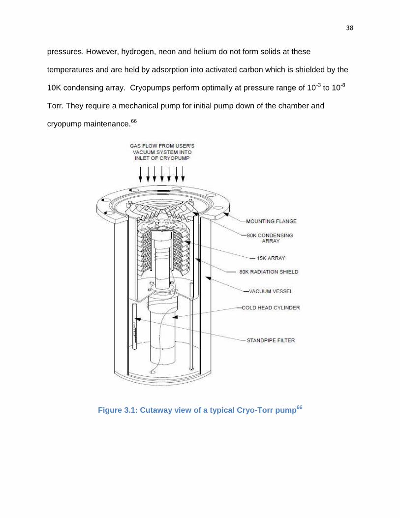
38
pressures. However, hydrogen, neon and helium do not form solids at these
temperatures and are held by adsorption into activated carbon which is shielded by the
10K condensing array. Cryopumps perform optimally at pressure range of 10-3 to 10-8
Torr. They require a mechanical pump for initial pump down of the chamber and
cryopump maintenance.66
Figure 3.1: Cutaway view of a typical Cryo-Torr pump66

39
3.3 Vacuum Measurement
The level of vacuum pressure can be monitored by several methods.63,64 There
are pressure gauges such as the capacitance diaphragm (Baratron) which monitor
directly from the force per area. There are indirect gauges such as the Pirani
(Convectron) which calculates the pressure from the thermal conductivity of the gas.
There is the indirect Bayard-Alpert (Ion Gauge) which ionizes and collects the gas
molecules to determine the pressure. Gauge types vary in pressure range
measurement capability. The type of gauge used is determined by the pressure level
requirements and often multiple gauge types are used in combination to effectively
measure varying pressure levels throughout the process. Fig. 3.2 shows the effective
pressure monitoring ranges of various gauges.63
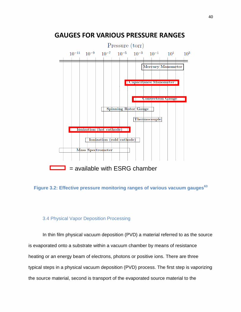
40
Figure 3.2: Effective pressure monitoring ranges of various vacuum gauges63
3.4 Physical Vapor Deposition Processing
In thin film physical vacuum deposition (PVD) a material referred to as the source
is evaporated onto a substrate within a vacuum chamber by means of resistance
heating or an energy beam of electrons, photons or positive ions. There are three
typical steps in a physical vacuum deposition (PVD) process. The first step is vaporizing
the source material, second is transport of the evaporated source material to the
GAUGES FOR VARIOUS PRESSURE RANGES
= available with ESRG chamber
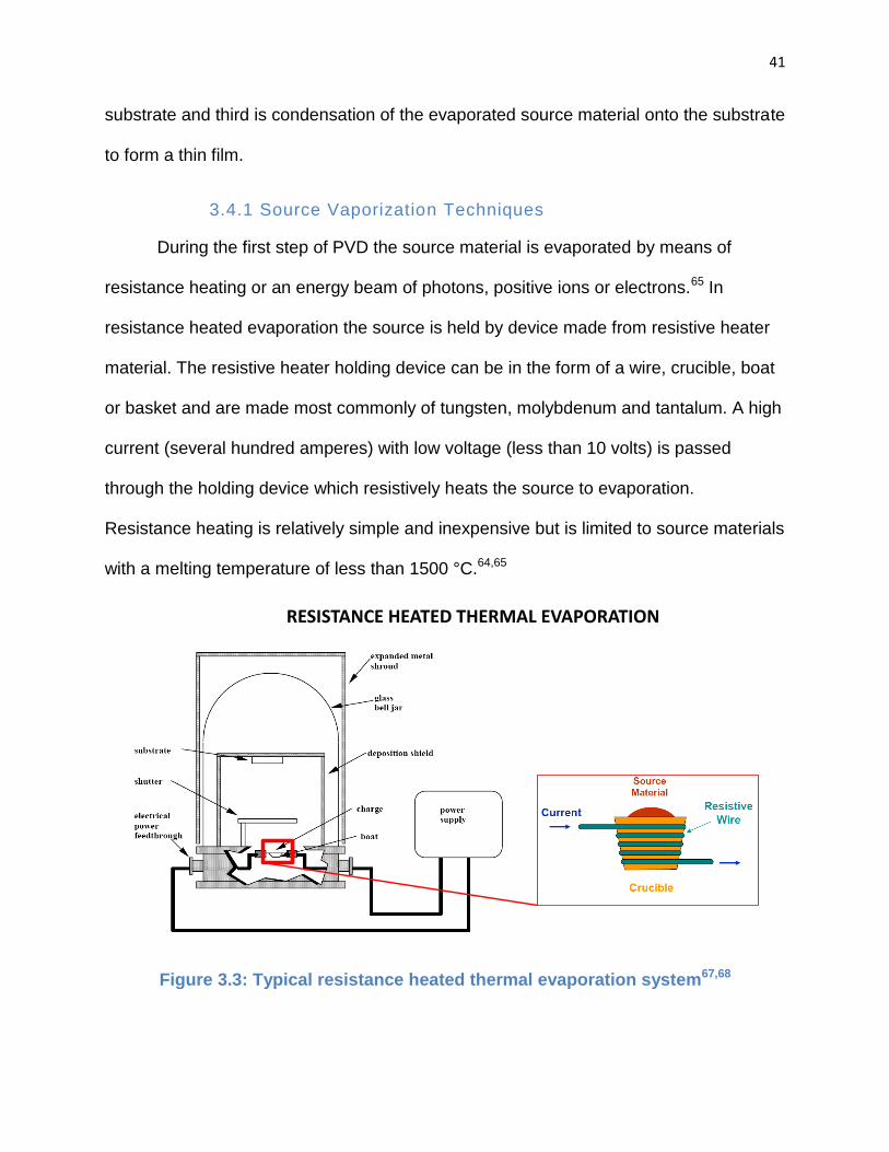
41
substrate and third is condensation of the evaporated source material onto the substrate
to form a thin film.
3.4.1 Source Vaporization Techniques
During the first step of PVD the source material is evaporated by means of
resistance heating or an energy beam of photons, positive ions or electrons.65 In
resistance heated evaporation the source is held by device made from resistive heater
material. The resistive heater holding device can be in the form of a wire, crucible, boat
or basket and are made most commonly of tungsten, molybdenum and tantalum. A high
current (several hundred amperes) with low voltage (less than 10 volts) is passed
through the holding device which resistively heats the source to evaporation.
Resistance heating is relatively simple and inexpensive but is limited to source materials
with a melting temperature of less than 1500 °C.64,65
Figure 3.3: Typical resistance heated thermal evaporation system67,68
RESISTANCE HEATED THERMAL EVAPORATION
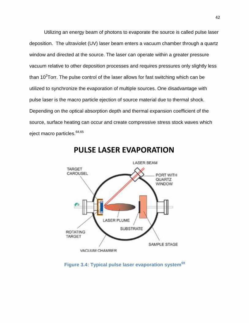
42
Utilizing an energy beam of photons to evaporate the source is called pulse laser
deposition. The ultraviolet (UV) laser beam enters a vacuum chamber through a quartz
window and directed at the source. The laser can operate within a greater pressure
vacuum relative to other deposition processes and requires pressures only slightly less
than 102Torr. The pulse control of the laser allows for fast switching which can be
utilized to synchronize the evaporation of multiple sources. One disadvantage with
pulse laser is the macro particle ejection of source material due to thermal shock.
Depending on the optical absorption depth and thermal expansion coefficient of the
source, surface heating can occur and create compressive stress stock waves which
eject macro particles.64,65
Figure 3.4: Typical pulse laser evaporation system69
PULSE LASER EVAPORATION
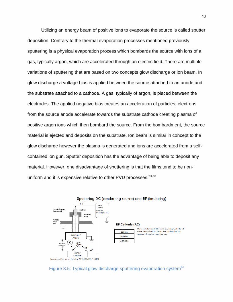
43
Utilizing an energy beam of positive ions to evaporate the source is called sputter
deposition. Contrary to the thermal evaporation processes mentioned previously,
sputtering is a physical evaporation process which bombards the source with ions of a
gas, typically argon, which are accelerated through an electric field. There are multiple
variations of sputtering that are based on two concepts glow discharge or ion beam. In
glow discharge a voltage bias is applied between the source attached to an anode and
the substrate attached to a cathode. A gas, typically of argon, is placed between the
electrodes. The applied negative bias creates an acceleration of particles; electrons
from the source anode accelerate towards the substrate cathode creating plasma of
positive argon ions which then bombard the source. From the bombardment, the source
material is ejected and deposits on the substrate. Ion beam is similar in concept to the
glow discharge however the plasma is generated and ions are accelerated from a self-
contained ion gun. Sputter deposition has the advantage of being able to deposit any
material. However, one disadvantage of sputtering is that the films tend to be non-
uniform and it is expensive relative to other PVD processes.64,65
Figure 3.5: Typical glow discharge sputtering evaporation system67
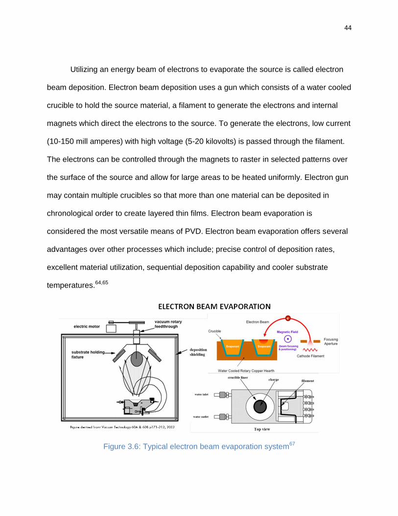
44
Utilizing an energy beam of electrons to evaporate the source is called electron
beam deposition. Electron beam deposition uses a gun which consists of a water cooled
crucible to hold the source material, a filament to generate the electrons and internal
magnets which direct the electrons to the source. To generate the electrons, low current
(10-150 mill amperes) with high voltage (5-20 kilovolts) is passed through the filament.
The electrons can be controlled through the magnets to raster in selected patterns over
the surface of the source and allow for large areas to be heated uniformly. Electron gun
may contain multiple crucibles so that more than one material can be deposited in
chronological order to create layered thin films. Electron beam evaporation is
considered the most versatile means of PVD. Electron beam evaporation offers several
advantages over other processes which include; precise control of deposition rates,
excellent material utilization, sequential deposition capability and cooler substrate
temperatures.64,65
Figure 3.6: Typical electron beam evaporation system67
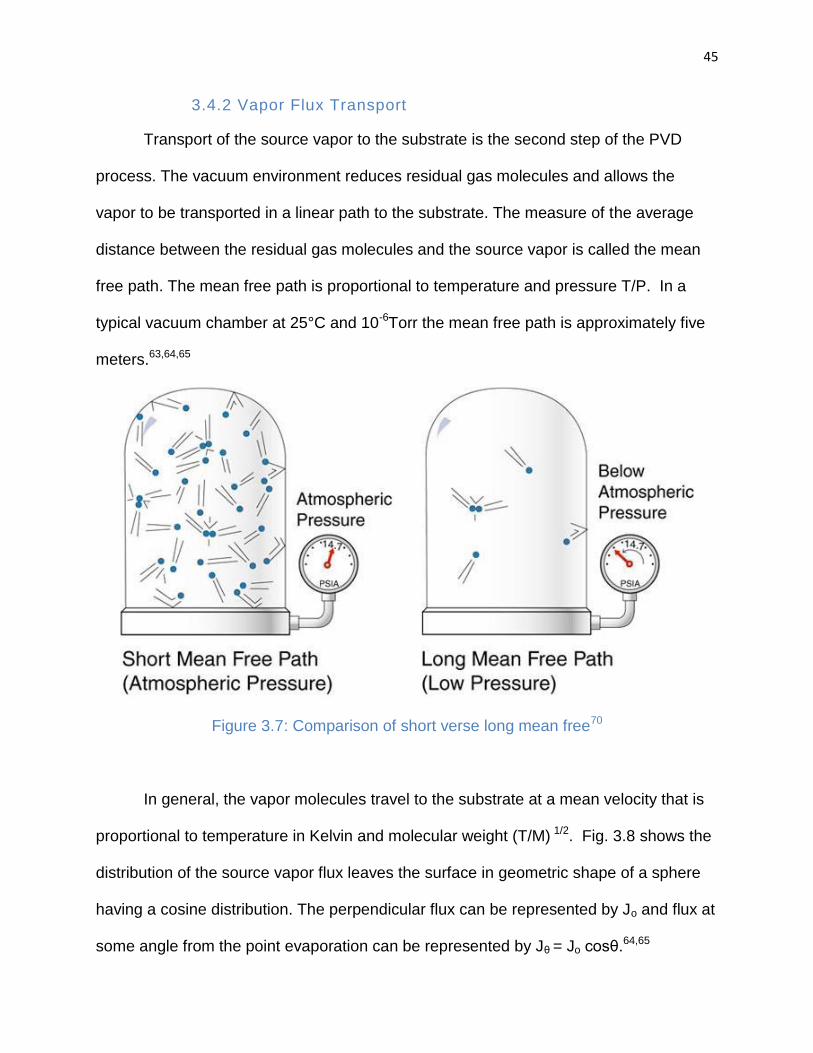
45
3.4.2 Vapor Flux Transport
Transport of the source vapor to the substrate is the second step of the PVD
process. The vacuum environment reduces residual gas molecules and allows the
vapor to be transported in a linear path to the substrate. The measure of the average
distance between the residual gas molecules and the source vapor is called the mean
free path. The mean free path is proportional to temperature and pressure T/P. In a
typical vacuum chamber at 25°C and 10-6Torr the mean free path is approximately five
meters.63,64,65
Figure 3.7: Comparison of short verse long mean free70
In general, the vapor molecules travel to the substrate at a mean velocity that is
proportional to temperature in Kelvin and molecular weight (T/M) 1/2. Fig. 3.8 shows the
distribution of the source vapor flux leaves the surface in geometric shape of a sphere
having a cosine distribution. The perpendicular flux can be represented by Jo and flux at
some angle from the point evaporation can be represented by Jθ = Jo cosθ.64,65
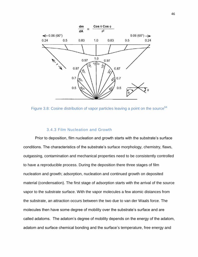
46
Figure 3.8: Cosine distribution of vapor particles leaving a point on the source64
3.4.3 Film Nucleation and Growth
Prior to deposition, film nucleation and growth starts with the substrate’s surface
conditions. The characteristics of the substrate’s surface morphology, chemistry, flaws,
outgassing, contamination and mechanical properties need to be consistently controlled
to have a reproducible process. During the deposition there three stages of film
nucleation and growth; adsorption, nucleation and continued growth on deposited
material (condensation). The first stage of adsorption starts with the arrival of the source
vapor to the substrate surface. With the vapor molecules a few atomic distances from
the substrate, an attraction occurs between the two due to van der Waals force. The
molecules then have some degree of mobility over the substrate’s surface and are
called adatoms. The adatom’s degree of mobility depends on the energy of the adatom,
adatom and surface chemical bonding and the surface’s temperature, free energy and
47
crystallographic plane orientation. The second stage of nucleation begins when the
adatoms lose mobility and form a nucleation site. With the presence of strong chemical
bonding between the adatom and surface, each surface atom can act as a nucleation
site. Without a strong chemical bond, the adatom will have high mobility. Preferential
nucleation sites will be created when the highly mobile adatoms arrive at surface
inconstancies such as lattice deflects (grain boundaries or point deflects), atomic steps,
impurities, crystallographic orientation or charge sites on insulating substrates. In
addition, highly mobile adatoms can collide with each other creating preferential
nucleation sites.64,65
Once nucleation sites are created, diffusion between the deposited atoms and
the substrate surface may occur to form an interfacial region. The adhesion and
electrical properties of the film are dependent on interfacial region. In the third stage of
growth, additional adatoms are collected on nucleation sites. The collection of adatoms
or growth occurs laterally over the surface which is called wetting or perpendicular to
the surface which is called dewetting. When there is weak chemical bonding between
the nuclei and surface dewetting growth typically occurs forming less dense films that
contain voids. In addition, weak bonding can create the nuclei to move like a liquid over
the surface and crystallography align with each other. Conversely, when the bond is
strong between the nuclei and surface wetting typically occurs. A special case called
epitaxial growth occurs when there is a strong bond with no interfacial region formation
and the nuclei’s orientation is influenced by the substrate’s surface crystallographic
orientation. In the cases where there is weak bonding, no interfacial region formed and
little substrate influence on growth, amorphous films typically form.
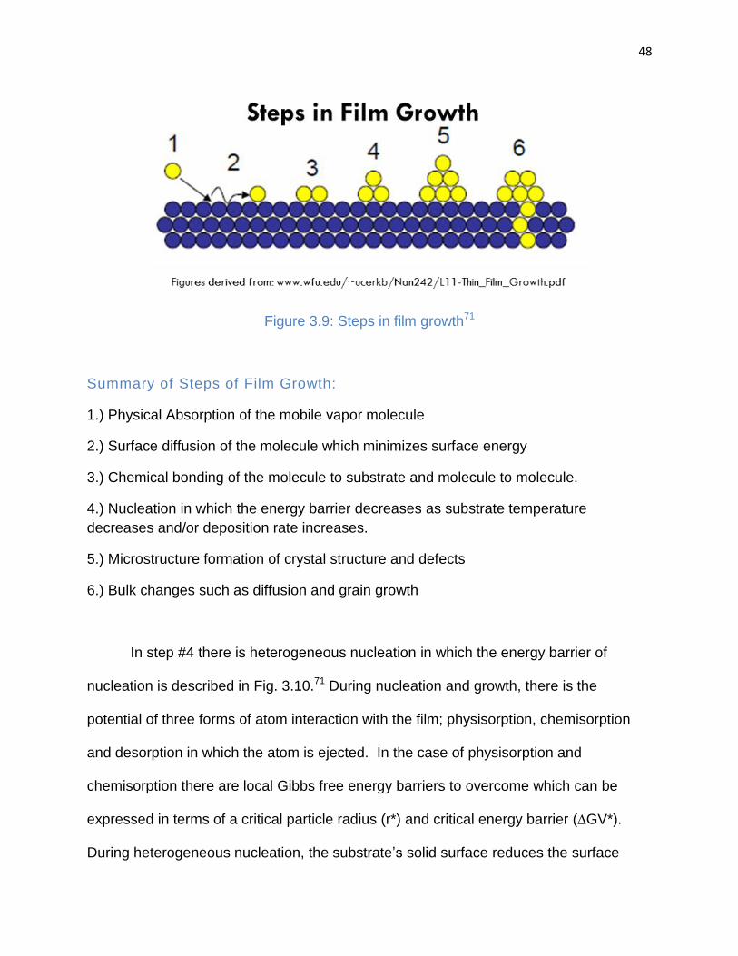
48
Figure 3.9: Steps in film growth71
Summary of Steps of Film Growth:
1.) Physical Absorption of the mobile vapor molecule
2.) Surface diffusion of the molecule which minimizes surface energy
3.) Chemical bonding of the molecule to substrate and molecule to molecule.
4.) Nucleation in which the energy barrier decreases as substrate temperature
decreases and/or deposition rate increases.
5.) Microstructure formation of crystal structure and defects
6.) Bulk changes such as diffusion and grain growth
In step #4 there is heterogeneous nucleation in which the energy barrier of
nucleation is described in Fig. 3.10.71 During nucleation and growth, there is the
potential of three forms of atom interaction with the film; physisorption, chemisorption
and desorption in which the atom is ejected. In the case of physisorption and
chemisorption there are local Gibbs free energy barriers to overcome which can be
expressed in terms of a critical particle radius (r*) and critical energy barrier (∆GV*).
During heterogeneous nucleation, the substrate’s solid surface reduces the surface
49
energy by reducing the surface area. Nucleation depends on the wetting angle and
relative surface energies produced from various interfaces such as between the
substrate and vapor, film and substrate and film and vapor. The adsorption of an atom
to the surface creates a tension in the surface atoms from stretching their bonds in
response to the new atom and this produces surface energy. Once the critical radius
and energy barrier are reached nucleation of the film will proceed.
Figure 3.10: Step #4 in Film Growth, Heterogeneous Nucleation71

50
3.4.4 Glancing Angle Deposition (GLAD)
The past decades have resulted in a number of new insights on effective
morphology controlled by variations in the static and dynamic substrate positioning. An
effort to design and fabricate a multifunctional electron beam deposition system with
capabilities including glancing angle, rocking through a programmable rotating substrate
drum was undertaken. The ability to design a servo motor controlled horizontally
rotating substrate drum that also exhibits the ability to adjust the deposition height in the
vertical direction presented an acute mechanical design challenge that is not addressed
by commercially available systems.
In a physical vapor deposition technique called glancing angle deposition
(GLAD), the morphology of the film growth can be controlled through substrate
rotational positioning at defined oblique angles to the source. Fig. 3.11 shows a typical
glancing angle deposition apparatus.72
51
Figure 3.11: Typical glancing angle deposition apparatus72
The oblique angle positioning of the substrate relative to the source creates a
lateral direction film growth component. This lateral film growth produces a shadowing
effect from the incident deposition flux shown in Fig. 3.12.72
ROTATIONα ROTATION
SOURCE
SUBSTRATEGLANCING ANGLE
β
β

52
Figure 3.12: Glancing angle shadow effect72
Columnar film morphology is the result of the shadow effect. Changing the
oblique angle positioning of the substrate relative to the source, changes the incident
flux direction and therefore changes the angular growth direction of the columnar film.
Rotating the oblique angled positioned substrate during the deposition will shape the
geometry of the columns. In addition to the rotation rate, the geometry of the columns
will have dependence on the deposition rate. By allowing the substrate to have a high
rotational rate relative to the deposition rate vertical columns will result. A lower
rotational rate relative to the deposition rate will produce helical columns. Fig. 3.13
shows the dependence of thin morphology on various process parameters.72,73,74
SHADOWED
REGION
VAPOR
FLUX β
SUBSTRATE
COLUMNAR
FILM
53
Figure 3.13: Description of various GLAD72,74
SLANTED NANOCOLUMNS:
Corresponds to holding axis α and
β fixed throughout the deposition
with glancing angle 30 < β <
80 .
VERTICAL NANOCOLUMNS:
Corresponds to rapidly rotating
axis α during the deposition.
HELICAL NANOCOLUMNS:
Corresponds to slowly rotating axis
α during the deposition.
CHEVRONS:
Corresponds rotating β axis
back and forth in 180
intervals. These are slanted
nanocolumns deposited on each
other with reversing directions.
BALL NANOCOLUMNS:
Corresponds to rapidly rotating
axis α and rotating axis β to
change the glancing angle
throughout the deposition.

54
4 Experimental Techniques
4.1 Preparation of the Thin Film Substrate (Current Collector)
Prior to the deposition the substrate, which served as the cell’s current collector,
was prepared using unpolished high-strength aluminum alloy 7075 (McMaster-Carr)
with a thickness of 0.8mm. The Al-7075 substrate was cut into a 25mm x 75mm strip
with the grains running parallel to the width of the strip. The Al-7075 strip was cleaned
using a Kimwipe® which was soaked in acetone, then cleaned with methanol and
placed in the center of a flat substrate holding plate along with two cleaned glass
microscope slides 25mm x 75mm with a thickness of 1mm. Fig. 4.1 shows the substrate
holding plate made of aluminum and the Al-7075 substrate and glass reference slides
attached. The glass slides were laid flat and place on each side of the Al-7075 strip and
the three pieces were secured to the substrate holding plate using Kapton® tape. The
glass slides were later used to measure film thickness with a stylus profilometer. Once
the film was deposited on the Al-7075 substrate and removed from the vacuum
chamber, 14.3 mm diameter discs to be used as the cathode and current collector
within the coin cell assembly were punched with a manual hand press such as the one
shown in Fig. 4.2.
Figure 4.1: Substrate holder showing attached Al-7075 strips and glass slide
55
Figure 4.2: Typical manual hand press used to punch the substrate/film into discs
4.2 Programming of the Dynamic Substrate Drum System
The positioning of the dynamic substrate drum was controlled through Ormec
servo motor hardware which included an F-Series PLC motion controller, power supply,
servo drive and servo motor. This hardware is shown in Fig. 4.3 along with the wiring
diagram that was used to assemble the components.73 The software used in the
dynamic substrate drum system was BASIC language loaded on a PC which interfaced
with the PLC motion controller. The positioning of the drum was based on a servo count
command (CNT) in which 77.625 CNT/degree. The drum rotation direction was +CNT
for counterclockwise and -CNT for clockwise.
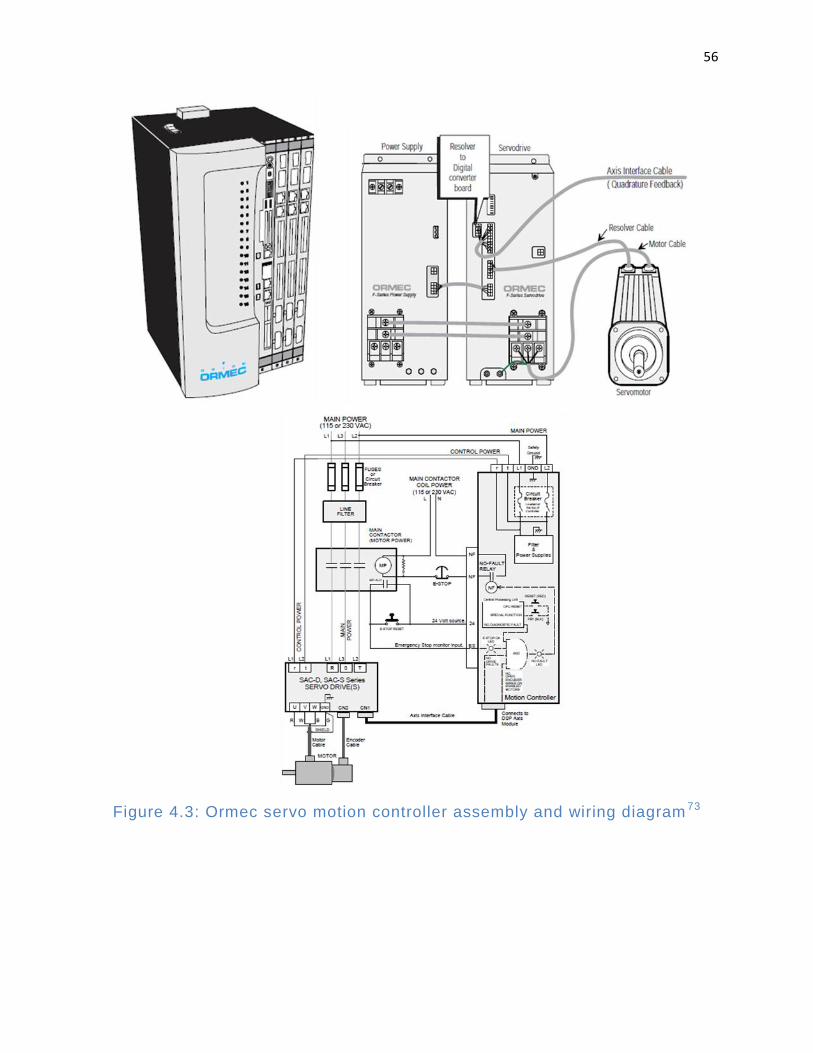
56
Figure 4.3: Ormec servo motion controller assembly and wiring diagram 73
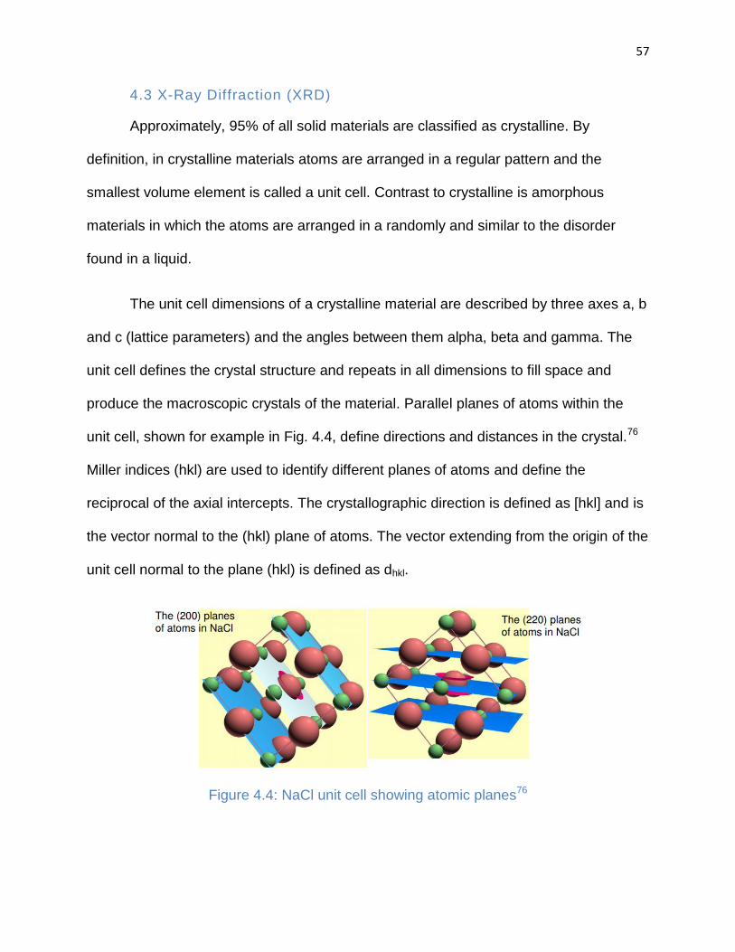
57
4.3 X-Ray Diffraction (XRD)
Approximately, 95% of all solid materials are classified as crystalline. By
definition, in crystalline materials atoms are arranged in a regular pattern and the
smallest volume element is called a unit cell. Contrast to crystalline is amorphous
materials in which the atoms are arranged in a randomly and similar to the disorder
found in a liquid.
The unit cell dimensions of a crystalline material are described by three axes a, b
and c (lattice parameters) and the angles between them alpha, beta and gamma. The
unit cell defines the crystal structure and repeats in all dimensions to fill space and
produce the macroscopic crystals of the material. Parallel planes of atoms within the
unit cell, shown for example in Fig. 4.4, define directions and distances in the crystal.76
Miller indices (hkl) are used to identify different planes of atoms and define the
reciprocal of the axial intercepts. The crystallographic direction is defined as [hkl] and is
the vector normal to the (hkl) plane of atoms. The vector extending from the origin of the
unit cell normal to the plane (hkl) is defined as dhkl.
Figure 4.4: NaCl unit cell showing atomic planes76
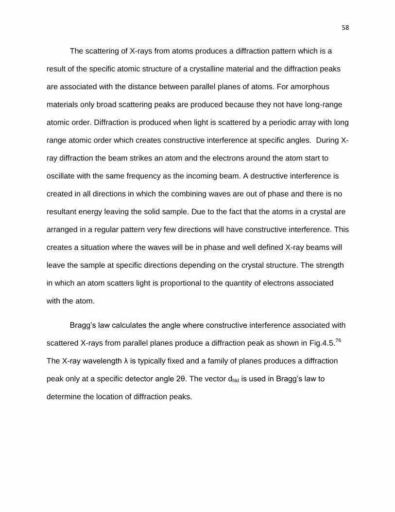
58
The scattering of X-rays from atoms produces a diffraction pattern which is a
result of the specific atomic structure of a crystalline material and the diffraction peaks
are associated with the distance between parallel planes of atoms. For amorphous
materials only broad scattering peaks are produced because they not have long-range
atomic order. Diffraction is produced when light is scattered by a periodic array with long
range atomic order which creates constructive interference at specific angles. During X-
ray diffraction the beam strikes an atom and the electrons around the atom start to
oscillate with the same frequency as the incoming beam. A destructive interference is
created in all directions in which the combining waves are out of phase and there is no
resultant energy leaving the solid sample. Due to the fact that the atoms in a crystal are
arranged in a regular pattern very few directions will have constructive interference. This
creates a situation where the waves will be in phase and well defined X-ray beams will
leave the sample at specific directions depending on the crystal structure. The strength
in which an atom scatters light is proportional to the quantity of electrons associated
with the atom.
Bragg’s law calculates the angle where constructive interference associated with
scattered X-rays from parallel planes produce a diffraction peak as shown in Fig.4.5.76
The X-ray wavelength λ is typically fixed and a family of planes produces a diffraction
peak only at a specific detector angle 2θ. The vector dhkl is used in Bragg’s law to
determine the location of diffraction peaks.

59
Figure 4.5: Definition of Bragg’s law76
The arrangement of atoms in the entire crystal determines the intensity of the
diffraction peaks. The diffraction peak is the result of summing the scattering from all the
(hkl) planes of atoms in the unit cell which can be described by the Fhkl equation in Fig.
4.6. The equation shows that the amplitude of scattered light is determined by where
the atoms are on the atomic planes and is expressed in terms of the fractional
coordinates xjyjzj. The scattering factor fj quantifies the efficiency of X-ray scattering at
any angle by the group of electrons in each atom and is equal to the number of
electrons around the atom at detector angle theta (θ)= 0° then drops off as θ increases.
Nj is the fraction of every equivalent position that is occupied by atom j.
Figure 4.6: Definition of diffraction peak intensity
For the experiments XRD was used for sample phase confirmation, determining
purity and orientation indentification. X-ray diffraction was performed on a Bruker D8
advanced diffractometer shown in the Fig. 4.7 with a CuKα source in the 2θ range from
20-37° and 48-65°at a scan rate of 0.06°/min.5 The range from 37-65°was removed

60
from the scan to due to large peaks from the Al-7075 substrate creating noise which
prevents evaluation of the thin film in this range. The samples were placed on a glass
slide and secured with Kapton™ tape on the edges. Once the scanning was completed
Eva and Topas software was used to analyze the raw data file to determine the
crystallite size, FWHM, peak height, dspacings and lattice parameters. To verify the
lattice parameters determined by Topas, an excel spreadsheet created at Durham
University and provided through their website was used along with the d-spacings from
Topas to calculate the lattice parameters.
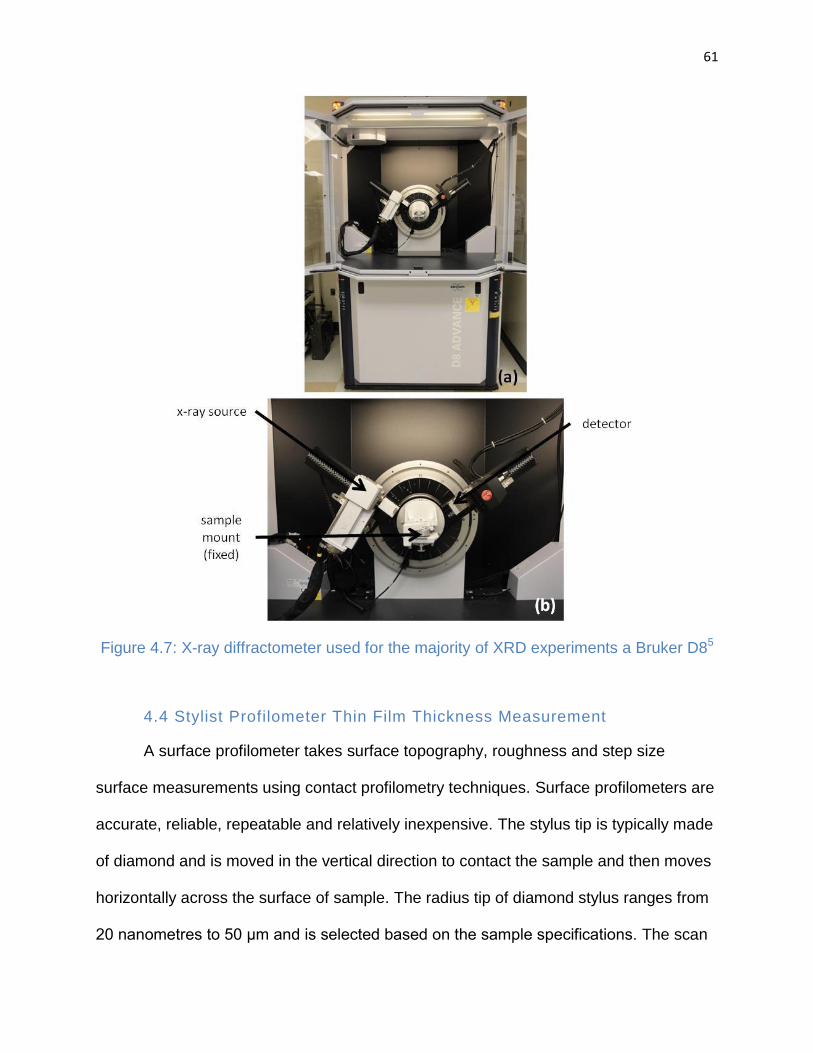
61
Figure 4.7: X-ray diffractometer used for the majority of XRD experiments a Bruker D85
4.4 Stylist Profilometer Thin Film Thickness Measurement
A surface profilometer takes surface topography, roughness and step size
surface measurements using contact profilometry techniques. Surface profilometers are
accurate, reliable, repeatable and relatively inexpensive. The stylus tip is typically made
of diamond and is moved in the vertical direction to contact the sample and then moves
horizontally across the surface of sample. The radius tip of diamond stylus ranges from
20 nanometres to 50 μm and is selected based on the sample specifications. The scan
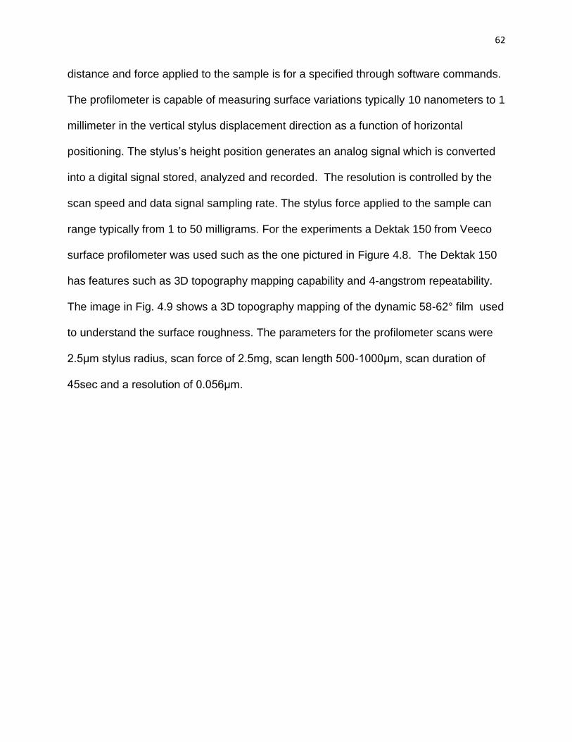
62
distance and force applied to the sample is for a specified through software commands.
The profilometer is capable of measuring surface variations typically 10 nanometers to 1
millimeter in the vertical stylus displacement direction as a function of horizontal
positioning. The stylus’s height position generates an analog signal which is converted
into a digital signal stored, analyzed and recorded. The resolution is controlled by the
scan speed and data signal sampling rate. The stylus force applied to the sample can
range typically from 1 to 50 milligrams. For the experiments a Dektak 150 from Veeco
surface profilometer was used such as the one pictured in Figure 4.8. The Dektak 150
has features such as 3D topography mapping capability and 4-angstrom repeatability.
The image in Fig. 4.9 shows a 3D topography mapping of the dynamic 58-62° film used
to understand the surface roughness. The parameters for the profilometer scans were
2.5μm stylus radius, scan force of 2.5mg, scan length 500-1000μm, scan duration of
45sec and a resolution of 0.056μm.
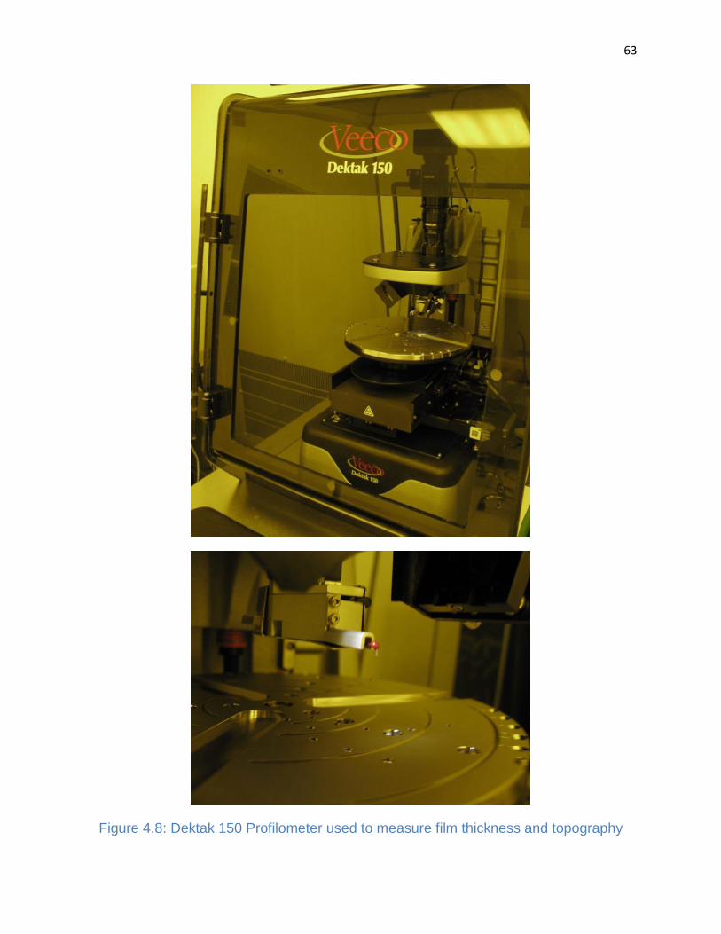
63
Figure 4.8: Dektak 150 Profilometer used to measure film thickness and topography
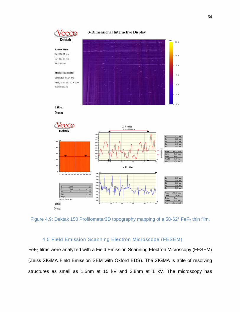
64
Figure 4.9: Dektak 150 Profilometer3D topography mapping of a 58-62° FeF2 thin film.
4.5 Field Emission Scanning Electron Microscope (FESEM)
FeF2 films were analyzed with a Field Emission Scanning Electron Microscopy (FESEM)
(Zeiss ΣIGMA Field Emission SEM with Oxford EDS). The ΣIGMA is able of resolving
structures as small as 1.5nm at 15 kV and 2.8nm at 1 kV. The microscopy has
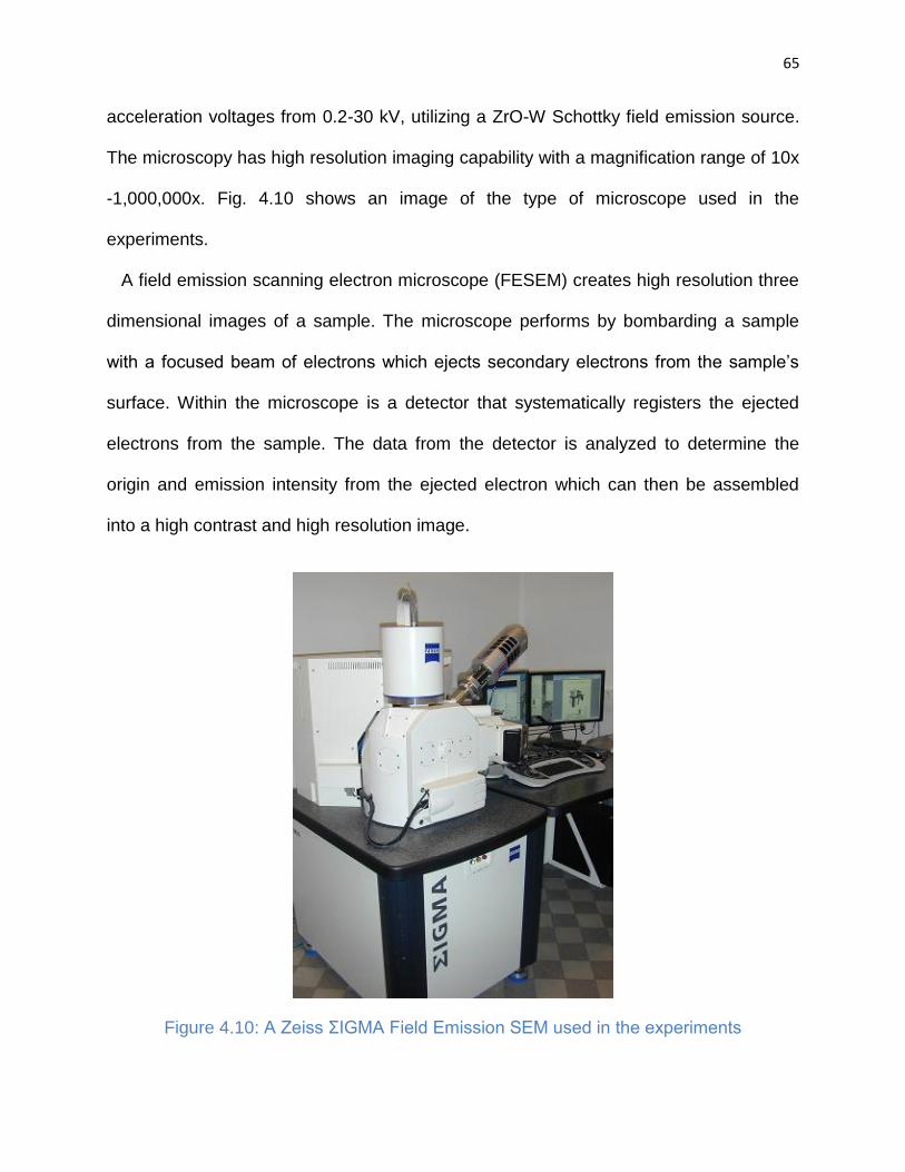
65
acceleration voltages from 0.2-30 kV, utilizing a ZrO-W Schottky field emission source.
The microscopy has high resolution imaging capability with a magnification range of 10x
-1,000,000x. Fig. 4.10 shows an image of the type of microscope used in the
experiments.
A field emission scanning electron microscope (FESEM) creates high resolution three
dimensional images of a sample. The microscope performs by bombarding a sample
with a focused beam of electrons which ejects secondary electrons from the sample’s
surface. Within the microscope is a detector that systematically registers the ejected
electrons from the sample. The data from the detector is analyzed to determine the
origin and emission intensity from the ejected electron which can then be assembled
into a high contrast and high resolution image.
Figure 4.10: A Zeiss ΣIGMA Field Emission SEM used in the experiments
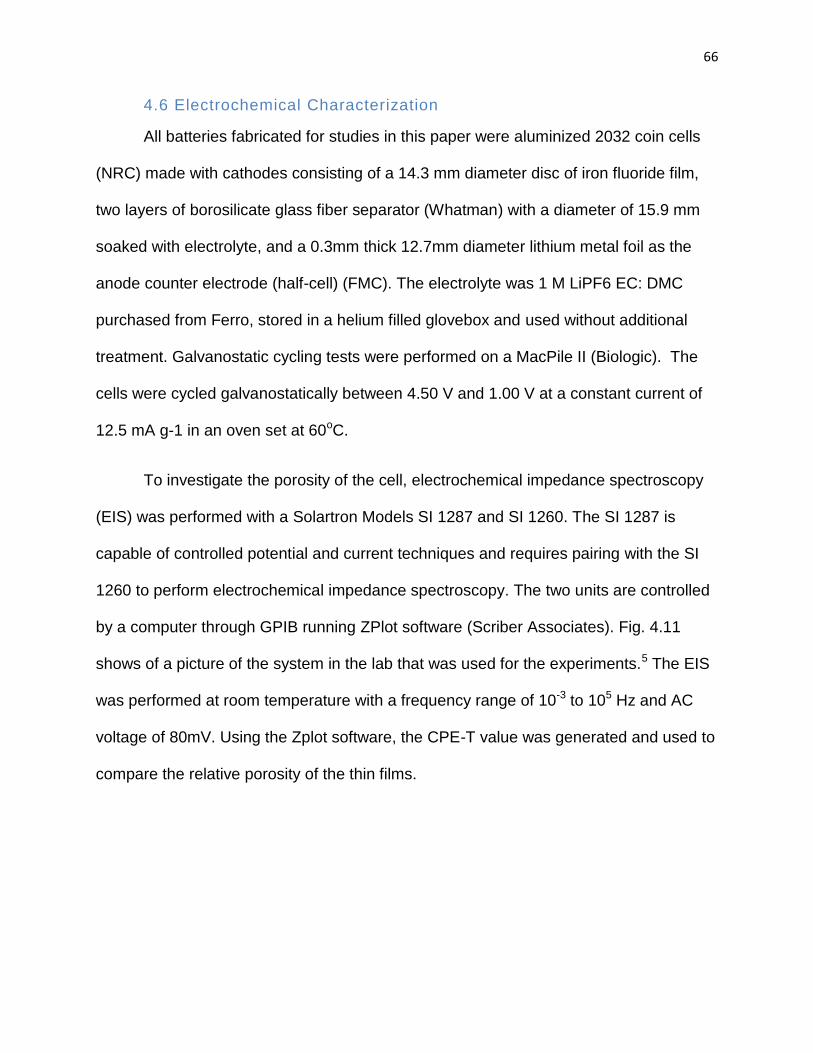
66
4.6 Electrochemical Characterization
All batteries fabricated for studies in this paper were aluminized 2032 coin cells
(NRC) made with cathodes consisting of a 14.3 mm diameter disc of iron fluoride film,
two layers of borosilicate glass fiber separator (Whatman) with a diameter of 15.9 mm
soaked with electrolyte, and a 0.3mm thick 12.7mm diameter lithium metal foil as the
anode counter electrode (half-cell) (FMC). The electrolyte was 1 M LiPF6 EC: DMC
purchased from Ferro, stored in a helium filled glovebox and used without additional
treatment. Galvanostatic cycling tests were performed on a MacPile II (Biologic). The
cells were cycled galvanostatically between 4.50 V and 1.00 V at a constant current of
12.5 mA g-1 in an oven set at 60oC.
To investigate the porosity of the cell, electrochemical impedance spectroscopy
(EIS) was performed with a Solartron Models SI 1287 and SI 1260. The SI 1287 is
capable of controlled potential and current techniques and requires pairing with the SI
1260 to perform electrochemical impedance spectroscopy. The two units are controlled
by a computer through GPIB running ZPlot software (Scriber Associates). Fig. 4.11
shows of a picture of the system in the lab that was used for the experiments.5 The EIS
was performed at room temperature with a frequency range of 10-3 to 105 Hz and AC
voltage of 80mV. Using the Zplot software, the CPE-T value was generated and used to
compare the relative porosity of the thin films.
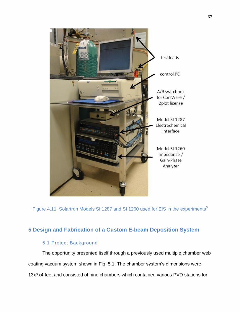
67
Figure 4.11: Solartron Models SI 1287 and SI 1260 used for EIS in the experiments5
5 Design and Fabrication of a Custom E-beam Deposition System
5.1 Project Background
The opportunity presented itself through a previously used multiple chamber web
coating vacuum system shown in Fig. 5.1. The chamber system’s dimensions were
13x7x4 feet and consisted of nine chambers which contained various PVD stations for
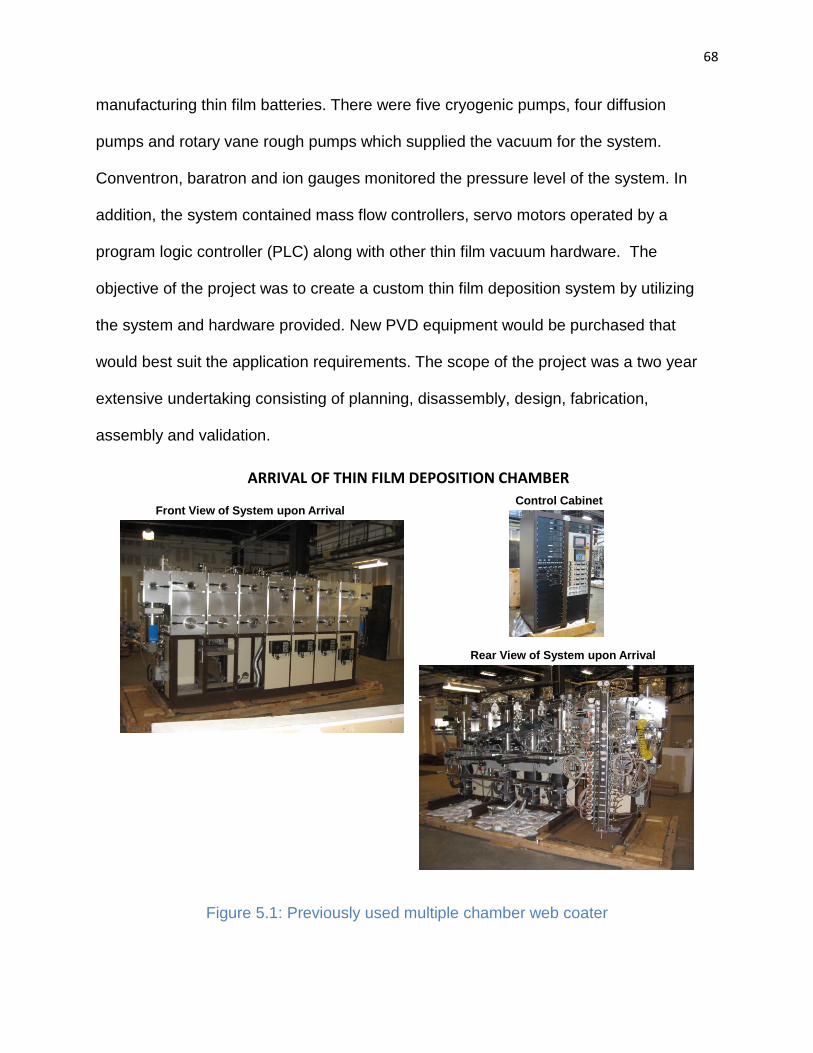
68
manufacturing thin film batteries. There were five cryogenic pumps, four diffusion
pumps and rotary vane rough pumps which supplied the vacuum for the system.
Conventron, baratron and ion gauges monitored the pressure level of the system. In
addition, the system contained mass flow controllers, servo motors operated by a
program logic controller (PLC) along with other thin film vacuum hardware. The
objective of the project was to create a custom thin film deposition system by utilizing
the system and hardware provided. New PVD equipment would be purchased that
would best suit the application requirements. The scope of the project was a two year
extensive undertaking consisting of planning, disassembly, design, fabrication,
assembly and validation.
Figure 5.1: Previously used multiple chamber web coater
ARRIVAL OF THIN FILM DEPOSITION CHAMBER
Front View of System upon Arrival
Rear View of System upon Arrival
Control Cabinet

69
5.2 Vacuum Chamber Preparation, Assembly and Testing
Before the arrival of the system into the lab the planning phase of the project took
place. A detailed schedule was made to estimate the timing to completion and to track
any unexpected items that would arise during the vacuum chamber development. This
schedule was a living document and was updated throughout the development. The
planning phase started in September 2009 and was completed in July of 2011. Fig. 5.2
shows the tracking schedule that was used throughout the development.
Due to the large size of the system there was a concern that the system would
not fit into the lab space. Footprint measurements, computer aided design drawings and
full scale templates were used to determine the best way to move the system into the
lab. It was determined that some disassembly of the system was required in order to
ensure a successful move. The two chambers on the ends of system had to be
disassembled along with pumps, vacuum piping and other external loose hardware.
After two months of disassembly and preparing the lab, the system was successfully
moved into the lab.

70
Figure 5.2: Detailed planning schedule for the vacuum chamber development
In addition to moving the system into the lab, the planning phase of the project
included selection of a newly purchased PVD system for the chamber. Extensive
investigation went into the types of e-beam systems and manufacturers prior to
purchasing the specific system. By reviewing the advantages and disadvantages of the
types of PVD systems it was determined that an e-beam would be best suited for the
applications the lab planned to pursue.
Once the system was moved into the lab, the phase of design, fabrication and
assembly started. It was determined that the chambers would be most functional as
independent vacuum chambers. The nine chambers would be divided into three
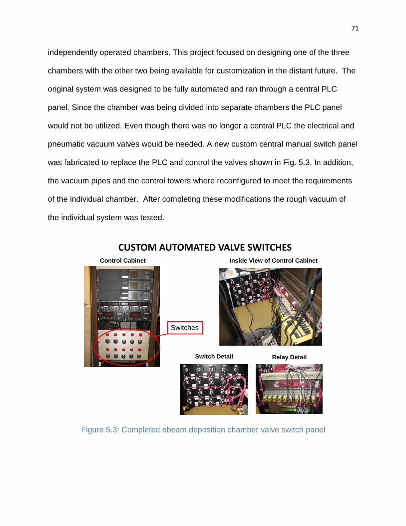
71
independently operated chambers. This project focused on designing one of the three
chambers with the other two being available for customization in the distant future. The
original system was designed to be fully automated and ran through a central PLC
panel. Since the chamber was being divided into separate chambers the PLC panel
would not be utilized. Even though there was no longer a central PLC the electrical and
pneumatic vacuum valves would be needed. A new custom central manual switch panel
was fabricated to replace the PLC and control the valves shown in Fig. 5.3. In addition,
the vacuum pipes and the control towers where reconfigured to meet the requirements
of the individual chamber. After completing these modifications the rough vacuum of
the individual system was tested.
Figure 5.3: Completed ebeam deposition chamber valve switch panel
CUSTOM AUTOMATED VALVE SWITCHES
Switches
Control Cabinet Inside View of Control Cabinet
Switch Detail Relay Detail
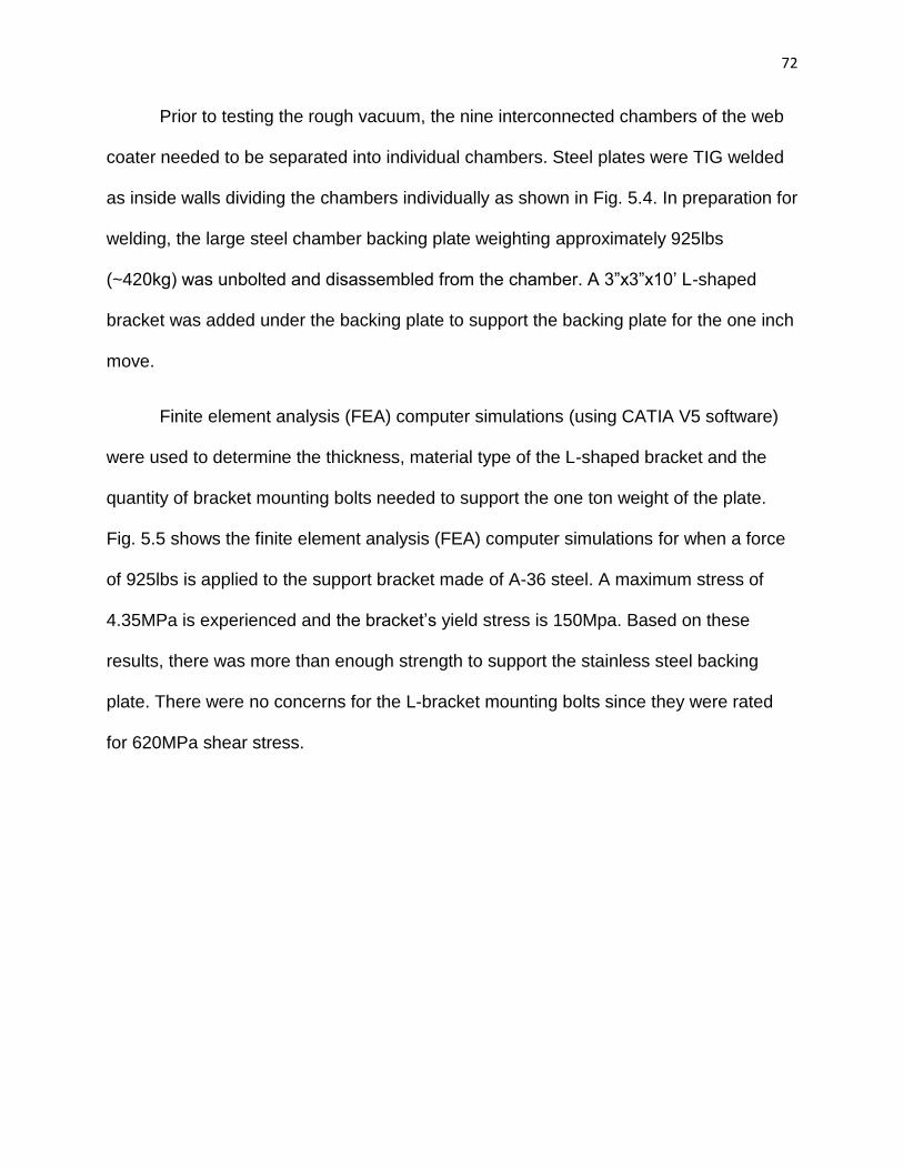
72
Prior to testing the rough vacuum, the nine interconnected chambers of the web
coater needed to be separated into individual chambers. Steel plates were TIG welded
as inside walls dividing the chambers individually as shown in Fig. 5.4. In preparation for
welding, the large steel chamber backing plate weighting approximately 925lbs
(~420kg) was unbolted and disassembled from the chamber. A 3”x3”x10’ L-shaped
bracket was added under the backing plate to support the backing plate for the one inch
move.
Finite element analysis (FEA) computer simulations (using CATIA V5 software)
were used to determine the thickness, material type of the L-shaped bracket and the
quantity of bracket mounting bolts needed to support the one ton weight of the plate.
Fig. 5.5 shows the finite element analysis (FEA) computer simulations for when a force
of 925lbs is applied to the support bracket made of A-36 steel. A maximum stress of
4.35MPa is experienced and the bracket’s yield stress is 150Mpa. Based on these
results, there was more than enough strength to support the stainless steel backing
plate. There were no concerns for the L-bracket mounting bolts since they were rated
for 620MPa shear stress.
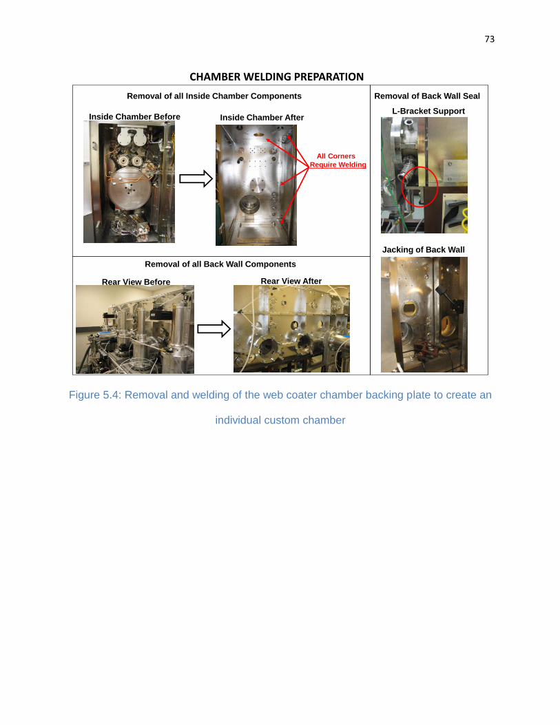
73
Figure 5.4: Removal and welding of the web coater chamber backing plate to create an
individual custom chamber
CHAMBER WELDING PREPARATION
Inside Chamber Before Inside Chamber After
Rear View Before Rear View After
Removal of all Back Wall Components
Removal of Back Wall SealRemoval of all Inside Chamber Components
All Corners
Require Welding
Jacking of Back Wall
L-Bracket Support
74
Figure 5.5: FEA simulation of chamber backing plate L-bracket support
The next stage of the project was to achieve high vacuum. During the removal of
the back plate the cryo pumps had to be removed from the backing plate. To evaluate
the high vacuum capability the cryo pumps were reassembled and connected to their
helium compressor. A chiller would need to be purchased that met the cooling rate
requirements of the compressor. To monitor the pressure during high vacuum an ion
gauge was installed. The chamber’s high vacuum capability was tested and achieved
1.0x10⁻⁷Torr. With the achievement of high vacuum the chamber was ready for the
design, fabrication and assembly of a novel thin film substrate holding drum and
electron beam deposition system.

75
5.3 Design of a Programmable Substrate Drum System
A programmable (BASIC language) servo motor controlled substrate holding
system was designed and fabricated with capability to produce glancing angle
morphologies. The system was designed with a novel horizontally rotating substrate
drum that also exhibits the ability to adjust the deposition height in the vertical direction.
Utilizing computer aided design (CAD) the system was initially developed in three
dimensions (3D). Referencing the 3D design, two dimensional (2D) drawings were
created to fabricate the individual components shown in Fig. 5.6.
Figure 5.6: 2D Fabrication drawings of the substrate drum system
76
During the design of the deposition system three key variables were considered
in order to control the glancing angle deposition morphology; the rotational velocity and
angular direction of the substrate drum, the height of the substrate relative to the source
and adjustment of the drum’s geometry.
The components for the chain gear system were purchased from McMaster Carr
and consisted of the following:
Roller Chain Idler Sprocket STL W/Needle Bearing, for #25 Chain, 19 Teeth,
1/2" Bore (Quantity of 5)
SS Machinable -Bore Roller Chain Sprocket for #25 Chain, 1/4" Pitch, 24 Teeth,
3/8" min Bore (Quantity of 2)
Stainless Steel ANSI Roller Chain 25SS Single Strand, 1/4" Pitch,
Rollerless,.130" Diameter, 5'L (Quantity of 1)
Considering these components along with the overall design of the custom substrate
drive system, the drum positional resolution was calculated. The substrate drum’s
positional resolution was calculated from the belt attached to the servo motor, having a
gear ratio of 100:1, to the drum where the substrate holder would be attached. Fig. 5.7
shows the result of the gear ratio summary to determine the substrate drum’s resolution.

77
Figure 5.7: Substrate drum positional resolution calculation
The control of the rotational velocity and angular direction of the substrate drum
was achieved through the use of a programmable servo motor. On the outside of the
vacuum chamber, the servo motor was attached to a ferrofluidic driveshaft feedthrough
by means of a belt. Inside of the chamber, the size 25 roller drive chain connected the
ferrofluidic driveshaft feedthrough to the substrate drum through the series of drive and
idler gears listed previously. Fig. 5.8 shows a schematic of the internal components of a
ferrofluidic driveshaft which holds a vacuum seal rated for 10-6 Torr by means of
magnetic fluid.77
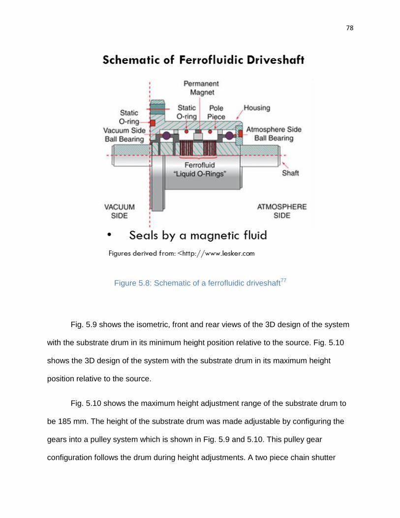
78
Figure 5.8: Schematic of a ferrofluidic driveshaft77
Fig. 5.9 shows the isometric, front and rear views of the 3D design of the system
with the substrate drum in its minimum height position relative to the source. Fig. 5.10
shows the 3D design of the system with the substrate drum in its maximum height
position relative to the source.
Fig. 5.10 shows the maximum height adjustment range of the substrate drum to
be 185 mm. The height of the substrate drum was made adjustable by configuring the
gears into a pulley system which is shown in Fig. 5.9 and 5.10. This pulley gear
configuration follows the drum during height adjustments. A two piece chain shutter
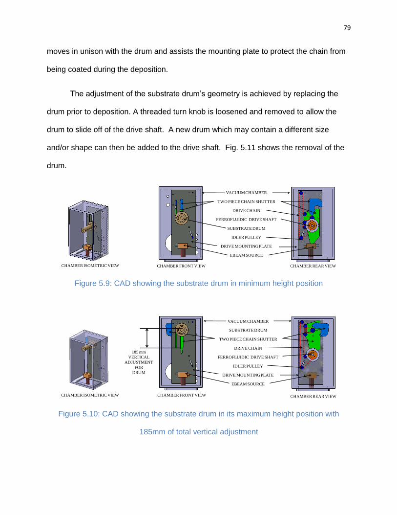
79
moves in unison with the drum and assists the mounting plate to protect the chain from
being coated during the deposition.
The adjustment of the substrate drum’s geometry is achieved by replacing the
drum prior to deposition. A threaded turn knob is loosened and removed to allow the
drum to slide off of the drive shaft. A new drum which may contain a different size
and/or shape can then be added to the drive shaft. Fig. 5.11 shows the removal of the
drum.
Figure 5.9: CAD showing the substrate drum in minimum height position
Figure 5.10: CAD showing the substrate drum in its maximum height position with
185mm of total vertical adjustment
VACUUM CHAMBER
TWO PIECE CHAIN SHUTTER
DRIVE CHAIN
FERROFLUIDIC DRIVE SHAFT
SUBSTRATE DRUM
IDLER PULLEY
DRIVE MOUNTING PLATE
EBEAM SOURCE
CHAMBER FRONT VIEW CHAMBER REAR VIEWCHAMBER ISOMETRIC VIEW
CHAMBER FRONT VIEW CHAMBER REAR VIEWCHAMBER ISOMETRIC VIEW
VACUUM CHAMBER
SUBSTRATE DRUM
TWO PIECE CHAIN SHUTTER
DRIVE CHAIN
FERROFLUIDIC DRIVE SHAFT
IDLER PULLEY
DRIVE MOUNTING PLATE
EBEAM SOURCE
185 mm
VERTICAL
ADJUSTMENT
FOR
DRUM
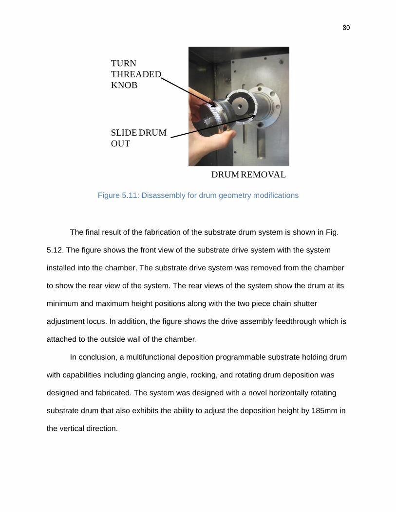
80
Figure 5.11: Disassembly for drum geometry modifications
The final result of the fabrication of the substrate drum system is shown in Fig.
5.12. The figure shows the front view of the substrate drive system with the system
installed into the chamber. The substrate drive system was removed from the chamber
to show the rear view of the system. The rear views of the system show the drum at its
minimum and maximum height positions along with the two piece chain shutter
adjustment locus. In addition, the figure shows the drive assembly feedthrough which is
attached to the outside wall of the chamber.
In conclusion, a multifunctional deposition programmable substrate holding drum
with capabilities including glancing angle, rocking, and rotating drum deposition was
designed and fabricated. The system was designed with a novel horizontally rotating
substrate drum that also exhibits the ability to adjust the deposition height by 185mm in
the vertical direction.
SLIDE DRUM
OUT
TURN
THREADED
KNOB
DRUM REMOVAL
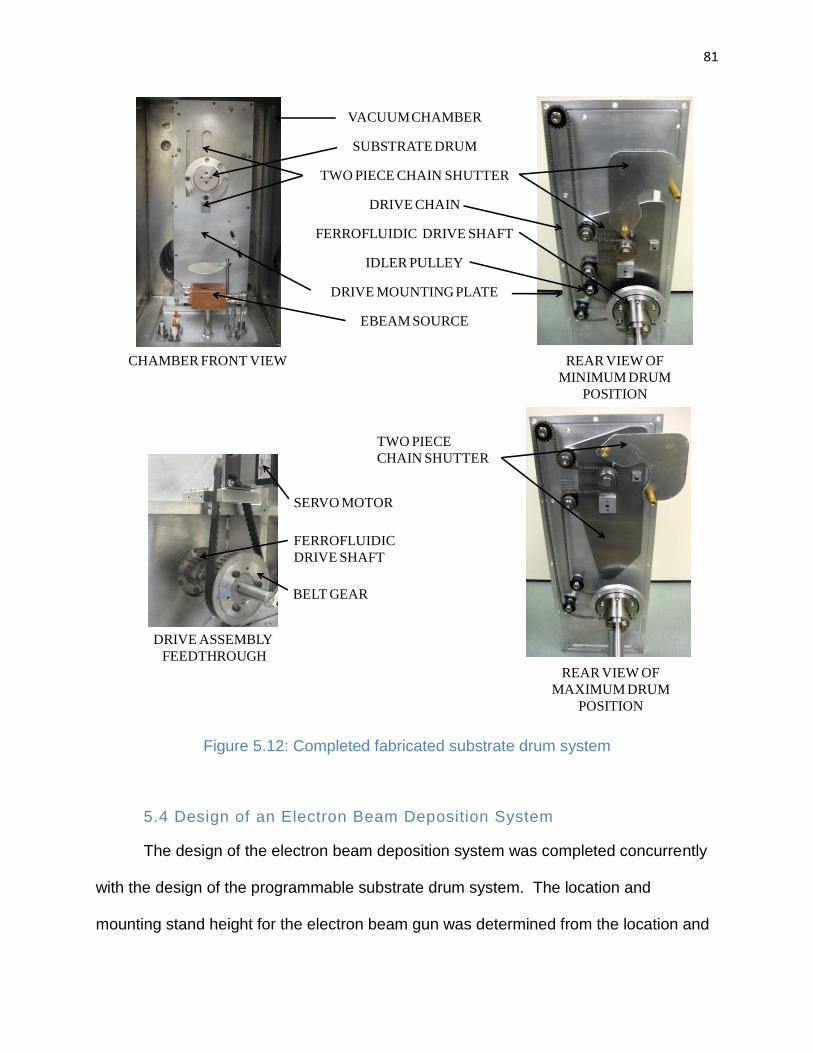
81
Figure 5.12: Completed fabricated substrate drum system
5.4 Design of an Electron Beam Deposition System
The design of the electron beam deposition system was completed concurrently
with the design of the programmable substrate drum system. The location and
mounting stand height for the electron beam gun was determined from the location and
VACUUM CHAMBER
SUBSTRATE DRUM
TWO PIECE CHAIN SHUTTER
DRIVE CHAIN
FERROFLUIDIC DRIVE SHAFT
IDLER PULLEY
DRIVE MOUNTING PLATE
EBEAM SOURCE
CHAMBER FRONT VIEW REAR VIEW OF
MINIMUM DRUM
POSITION
TWO PIECE
CHAIN SHUTTER
BELT GEAR
FERROFLUIDIC
DRIVE SHAFT
SERVO MOTOR
DRIVE ASSEMBLY
FEEDTHROUGH
REAR VIEW OF
MAXIMUM DRUM
POSITION
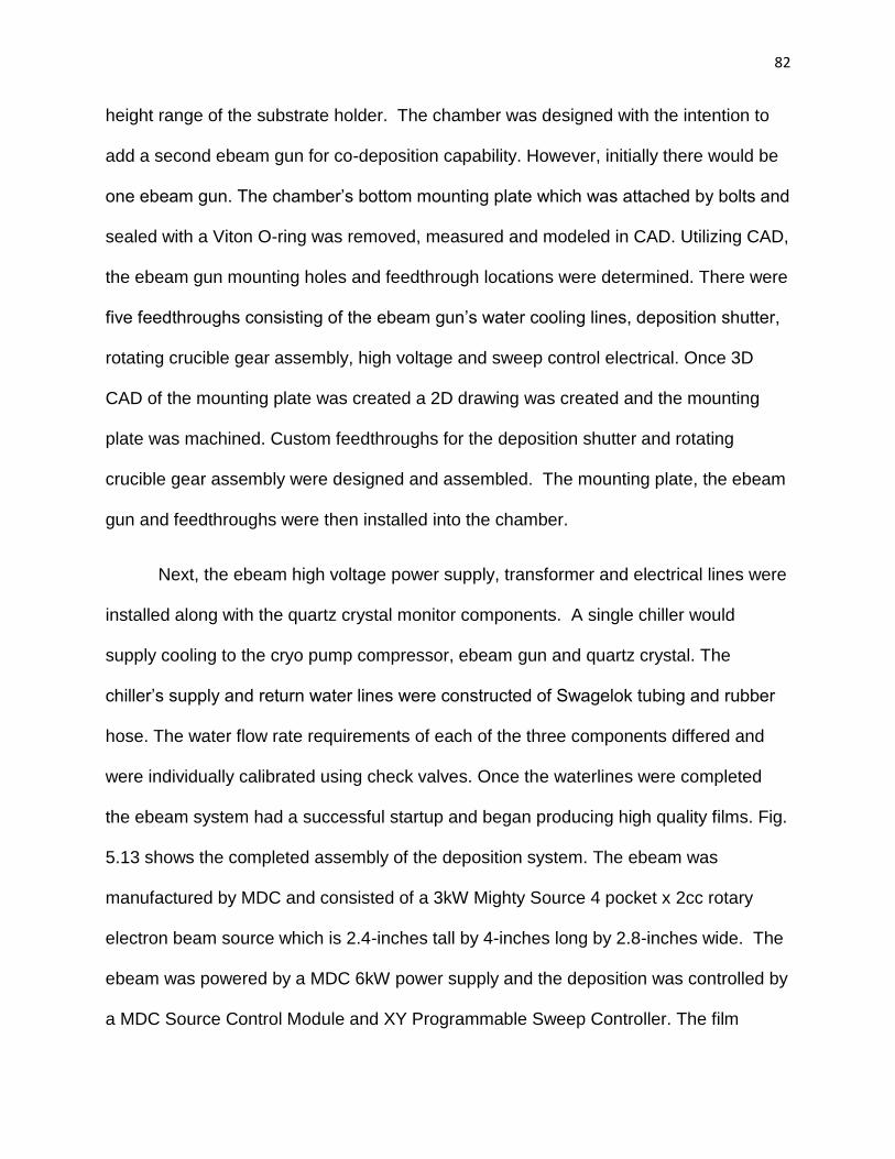
82
height range of the substrate holder. The chamber was designed with the intention to
add a second ebeam gun for co-deposition capability. However, initially there would be
one ebeam gun. The chamber’s bottom mounting plate which was attached by bolts and
sealed with a Viton O-ring was removed, measured and modeled in CAD. Utilizing CAD,
the ebeam gun mounting holes and feedthrough locations were determined. There were
five feedthroughs consisting of the ebeam gun’s water cooling lines, deposition shutter,
rotating crucible gear assembly, high voltage and sweep control electrical. Once 3D
CAD of the mounting plate was created a 2D drawing was created and the mounting
plate was machined. Custom feedthroughs for the deposition shutter and rotating
crucible gear assembly were designed and assembled. The mounting plate, the ebeam
gun and feedthroughs were then installed into the chamber.
Next, the ebeam high voltage power supply, transformer and electrical lines were
installed along with the quartz crystal monitor components. A single chiller would
supply cooling to the cryo pump compressor, ebeam gun and quartz crystal. The
chiller’s supply and return water lines were constructed of Swagelok tubing and rubber
hose. The water flow rate requirements of each of the three components differed and
were individually calibrated using check valves. Once the waterlines were completed
the ebeam system had a successful startup and began producing high quality films. Fig.
5.13 shows the completed assembly of the deposition system. The ebeam was
manufactured by MDC and consisted of a 3kW Mighty Source 4 pocket x 2cc rotary
electron beam source which is 2.4-inches tall by 4-inches long by 2.8-inches wide. The
ebeam was powered by a MDC 6kW power supply and the deposition was controlled by
a MDC Source Control Module and XY Programmable Sweep Controller. The film
83
thickness was controlled by an Inficon SQC-310 Series deposition controller and quartz
crystal sensor.
Figure 5.13: Picture of the completed ebeam deposition system
The chamber system operational readiness was validated through the
conformation of producing specific selections of thin film materials. These materials
included titanium, lithium fluoride, iron fluoride. The materials were selected based on
their familiarity to the lab (being PVD film materials that the lab has produced in the
past) and their applicability to the research goals of this thesis.
The vaccum chamber achieved an initial base pressure of 1x10^-7Torr before
feedthroughs were added which then raised the base pressure to 5x10⁻⁷Torr that
required 8 hours of overnight pumping. To save pump down time the depositions for
the experiments were conducted at 3x10⁻⁶Torr. The chamber took 2.5 hours to achieve
COMPLETED CHAMBER SYSTEM AT ESRG
REAR VIEW OF SYSTEM FRONT VIEW OF SYSTEM
SUBSTRATE DRUM PLC
84
this pressure level and consisted of pumping for 1.5 hours with a Leybold D16B Trivac
Rotary Vane Dual Stage Mechanical Vacuum Pump until the pressure reached to 1x10-
3Torr and then 1 hour of high vacuum pumping with the two CTI-Cryogenics-8 cryo
pumps. The rate of rise (ROR) of the chamber when the cryo pumps gates were closed
at an initial chamber pressure of 3x10⁻⁶Torr was 2.5Torr over 2 minutes then stabilized
to less than 50millTorr per hour.
Titanium was selected for the first thin film material to validate due to its stable
deposition evaporation rate, high melt temperature, solid pellet source form and the
extensive PVD experience the lab has with producing films of this material. The first
step in validating the system was to calibrate the quartz crystal thickness monitor
(QCM) and determine a tooling factor for titanium. The source material of titanium was
of pellet form and placed into a 2cc graphite crucible. To calibrate the QCM, titanium
was deposited on a substrate consisting of three glass slides (1”x3” each) that were
placed ten inches from the source. During the deposition the ebeam current was set at
100mA and a voltage of 5kV which produced a QCM reading of 2 angstroms per
second (A°/sec). The vacuum pressure was 3x10⁻⁶Torr before the deposition, then the
pressure rose to 8x10⁻⁶Torr for the first 5 minutes of the deposition and then stabilized
back to 3x10⁻⁶Torr for the remaining duration. Since the crystal of the QCM was located
eighteen inches from the source (ebeam) and the substrate nine inches from the source
(ebeam), the deposition readings of the QCM were underestimating the rate. To
determine a tooling factor for the QCM four independent depositions were completed
and the thickness of the film on the glass slides was measured between each
deposition. The thickness of the film was measured using a Dektak 150 stylus surface
85
profiler. Taking the actual measured thickness of the film and dividing it by the QCM
thickness reading determined the tooling factor for titanium. The tooling factor for
titanium was calculated to be approximately 4.0. By multiplying the tooling factor by the
QCM deposition rate of 2A°/sec it was determined that the actual deposition rate during
the first four depositions was approximately 8 A°/sec. This identical QCM calibration
procedure would be needed for each new material that the system deposited in order to
have an accurate understanding of the real time QCM readings. The second step of the
validating the system was to center the electron beam with the center of the source
crucible. With the initial depositions set at 5.0kV and inspecting the solidified previously
melted source material in the crucible the beam alignment was determined. A visual
inspection of the solidified source for a concaved region indicated the contact position of
the beam. Over the next three depositions, the voltage was adjusted to 4.6kV, 4.8kV
and 4.75kV respectively to align the electron beam with the crucible center. Once the
electron beam was initially centered it would not require centering with new source
materials and would be set at 4.75kV moving forward. Fig. 5.14 shows the Dektak
profiler thickness results of the first titanium deposition with 4.75kV and the electron
beam centered.
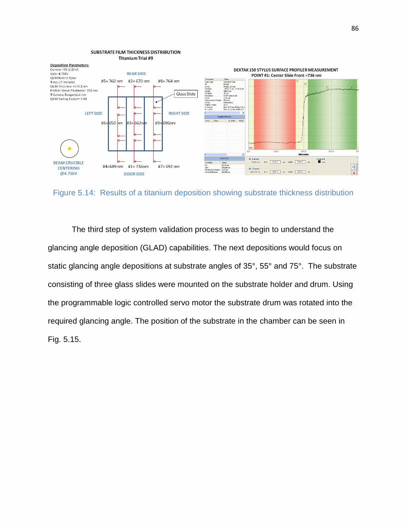
86
Figure 5.14: Results of a titanium deposition showing substrate thickness distribution
The third step of system validation process was to begin to understand the
glancing angle deposition (GLAD) capabilities. The next depositions would focus on
static glancing angle depositions at substrate angles of 35°, 55° and 75°. The substrate
consisting of three glass slides were mounted on the substrate holder and drum. Using
the programmable logic controlled servo motor the substrate drum was rotated into the
required glancing angle. The position of the substrate in the chamber can be seen in
Fig. 5.15.
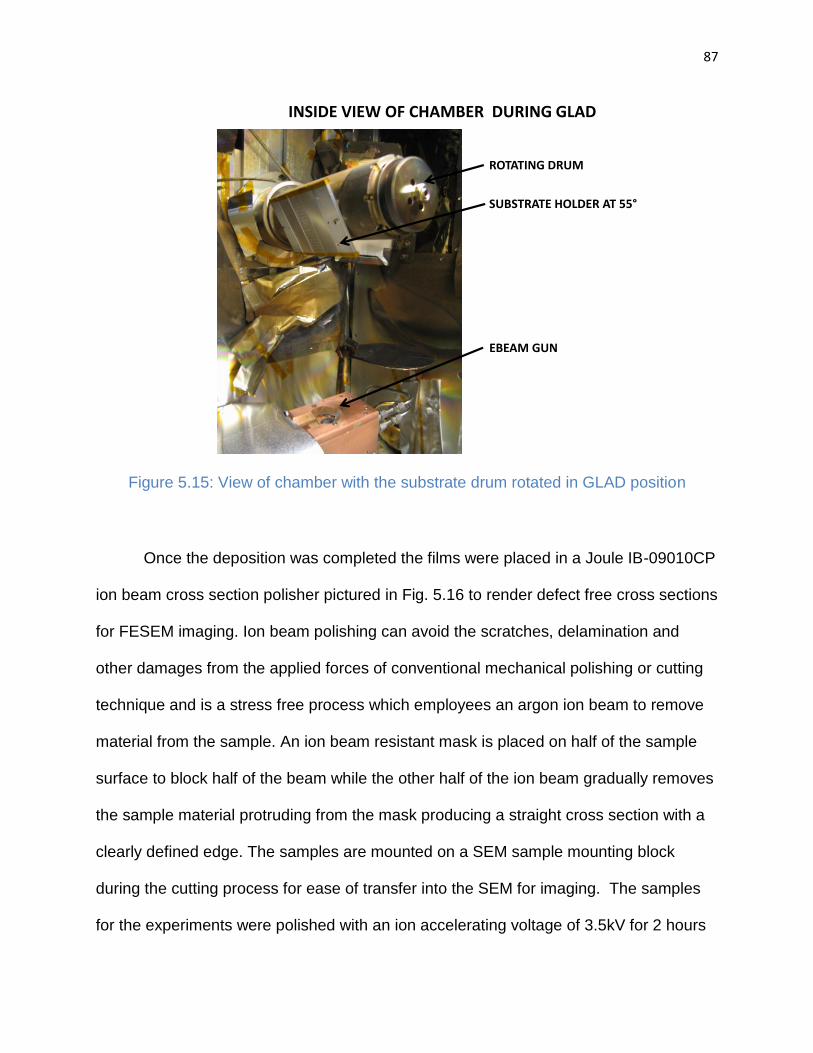
87
Figure 5.15: View of chamber with the substrate drum rotated in GLAD position
Once the deposition was completed the films were placed in a Joule IB-09010CP
ion beam cross section polisher pictured in Fig. 5.16 to render defect free cross sections
for FESEM imaging. Ion beam polishing can avoid the scratches, delamination and
other damages from the applied forces of conventional mechanical polishing or cutting
technique and is a stress free process which employees an argon ion beam to remove
material from the sample. An ion beam resistant mask is placed on half of the sample
surface to block half of the beam while the other half of the ion beam gradually removes
the sample material protruding from the mask producing a straight cross section with a
clearly defined edge. The samples are mounted on a SEM sample mounting block
during the cutting process for ease of transfer into the SEM for imaging. The samples
for the experiments were polished with an ion accelerating voltage of 3.5kV for 2 hours
ROTATING DRUM
SUBSTRATE HOLDER AT 55°
EBEAM GUN
INSIDE VIEW OF CHAMBER DURING GLAD
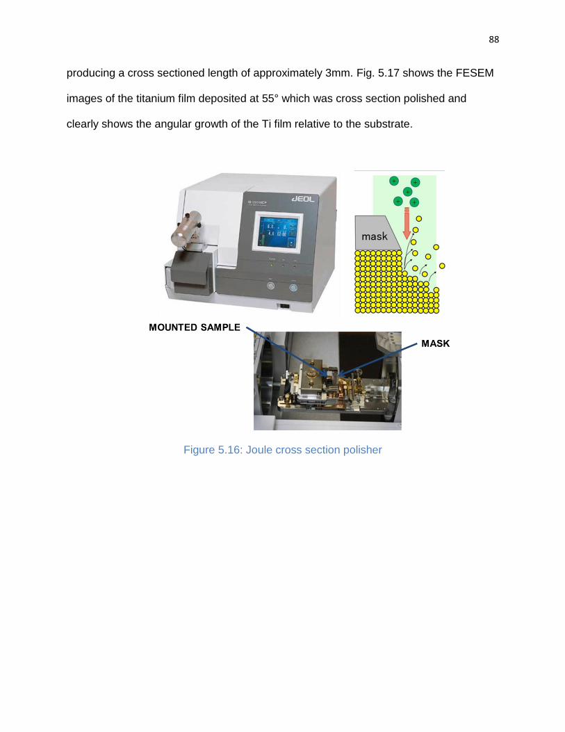
88
producing a cross sectioned length of approximately 3mm. Fig. 5.17 shows the FESEM
images of the titanium film deposited at 55° which was cross section polished and
clearly shows the angular growth of the Ti film relative to the substrate.
Figure 5.16: Joule cross section polisher
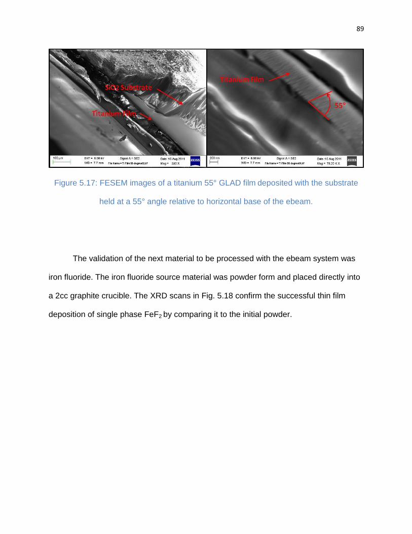
89
Figure 5.17: FESEM images of a titanium 55° GLAD film deposited with the substrate
held at a 55° angle relative to horizontal base of the ebeam.
The validation of the next material to be processed with the ebeam system was
iron fluoride. The iron fluoride source material was powder form and placed directly into
a 2cc graphite crucible. The XRD scans in Fig. 5.18 confirm the successful thin film
deposition of single phase FeF2 by comparing it to the initial powder.
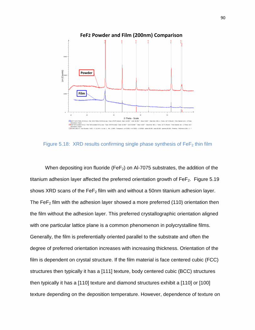
90
Figure 5.18: XRD results confirming single phase synthesis of FeF2 thin film
When depositing iron fluoride (FeF2) on Al-7075 substrates, the addition of the
titanium adhesion layer affected the preferred orientation growth of FeF2. Figure 5.19
shows XRD scans of the FeF2 film with and without a 50nm titanium adhesion layer.
The FeF2 film with the adhesion layer showed a more preferred (110) orientation then
the film without the adhesion layer. This preferred crystallographic orientation aligned
with one particular lattice plane is a common phenomenon in polycrystalline films.
Generally, the film is preferentially oriented parallel to the substrate and often the
degree of preferred orientation increases with increasing thickness. Orientation of the
film is dependent on crystal structure. If the film material is face centered cubic (FCC)
structures then typically it has a [111] texture, body centered cubic (BCC) structures
then typically it has a [110] texture and diamond structures exhibit a [110] or [100]
texture depending on the deposition temperature. However, dependence of texture on
MATT FeF2 TRIAL #3 9-9-11
00-045-1062 (*) - Iron Fluoride - FeF2 - Y: 31.24 % - d x by: 1. - WL: 1.5406 - Tetragonal - a 4.70350 - b 4.70350 - c 3.30560 - alpha 90.000 - beta 90.000 - gamma 90.000 - Primitive - P42/mnm (136) - 2 - 7
Operations: Import
Matt FeF2 powder 9-9-11 - File: FeF2 powder 9-9-11.raw - Type: 2Th/Th locked - Start: 10.000 ° - End: 59.999 ° - Step: 0.020 ° - Step time: 306. s - Temp.: 25 °C (Room) - Time Started: 18 s - 2-Theta: 10.0
Operations: Import
MATT FeF2 TRIAL #3 9-9-11 - File: FeF2 TRIAL #3 9-9-11.raw - Type: 2Th/Th locked - Start: 15.000 ° - End: 60.005 ° - Step: 0.020 ° - Step time: 306. s - Temp.: 25 °C (Room) - Time Started: 16 s - 2-Theta
Lin
(C
ounts
)
0
10000
20000
30000
2-Theta - Scale
14 20 30 40 50
[1,1
,0]
[1,0
,1]
[1,1
,1]
[2,1
,0]
[2,1
,1]
[2,2
,0]
[0,0
,2]
FeF2 Powder and Film (200nm) Comparison
Powder
Film

91
crystal structure is not assumed and different mechanisms can produce or modify
texture. These mechanisms include the substrate temperature, pressure during the
deposition, crystallographic orientation of the substrate, deposition rate and in addition,
texturing can be caused by the tendency to minimize volume strain energy in thicker
films and minimize the surface energy in very thin films. 31,78,79,80,81,82 Considering that
these FeF2 films with and without the titanium adhesion layer were deposited with the
same thickness and process parameters, it is likely that the texturing was produced
from the crystallographic orientation differences between the aluminum (FCC) and
titanium (HCP).
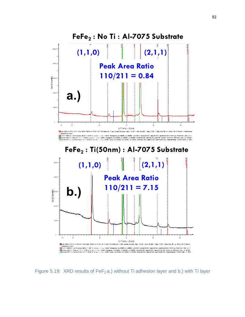
92
Figure 5.19: XRD results of FeF2 a.) without Ti adhesion layer and b.) with Ti layer
93
6 Effect of Vertically Structured Porosity on Electrochemical
Performance of FeF2 Films
6.1 Introduction
There is an increasing demand for high capacity power sources in applications of
portable electronics and large scale mobile devices such as electric vehicles. However,
commercial lithium batteries typically use intercalation cathode compounds (e.g.,
LiFePO4, LiCoO2) which have moderate energy density and do not meet the growing
demand for higher energy technology. While intercalation materials offer desirable
properties such as good cycling life, good rate capability, and high discharge voltages,
they are restricted at most to a single electron transfer per formula unit. This restriction
limits the energy density that can be achieved with current insertion materials.
In order to achieve higher specific capacity, an alternative process known as
conversion reaction has been studied for decades as electrodes for primary batteries
but only more recently for secondary.83-87 In conversion reactions, larger theoretical
energy densities are possible because this reaction can utilize all energetically favorable
oxidation states of the metal cation that comprises the cathode. As a result, more than
one electron transfer occurs per transition metal (TM) cation during the redox cycle.
Although, reversible conversion reactions have been demonstrated with a variety of
materials including metal sulfides88,89, oxides90,91,92, fluorides93,94, nitrides95,96 and
phosphides97,98 only metal fluorides have a high enough reaction potential to be used as
Li-ion cathodes. This is due to the very ionic nature of the metal fluoride bond.
Despite metal fluorides represent a route for high energy density positive
electrodes they are limited by their wide band gap corresponding in electronically
94
insulating behavior and very poor ionic diffusion through the conversion front. Transport
is greatly enhanced by the use of carbon or mixed conducting matrices in combination
with metal fluoride domains <30nm. This approach has enabled the electrochemical
activity of a wide variety of metal fluorides.99 Despite the improvements, conversion
reaction mechanisms are not well understood and the opportunity to commercialize
these electrodes is obstructed by cycling performance issues most notably cycling
retention and reversibility.
This study investigates the conversion cathode material iron fluoride (FeF2) to
further understand conversion reaction mechanisms. FeF2 has a rutile tetragonal
structure and is an attractive material for use as nanocomposite cathodes due to its
exceptionally high specific theoretical capacity of 571mAh/g. In addition, the rutile
difluoride is ubiquitous among the other first row transition metal fluorides such as NiF2
and CoF2 which are also of interest for electrochemical applications. During the reaction
FeF2 + Li+ combine to form nanocrystalline LiF crystals and Fe0 clusters which is
represented in eq 1.
FeF2 + 2Li ↔ 2LiF + Fe (1)
This study uses a combination of dense and highly structured thin films to (a)
elucidate the relative contributions of the ionic and electronic transport processes in the
rate and cycling limitations of the electrochemical cell, (b) the effect of the electrode
structure to absorb the 16.7% electrode expansion on cycling through the reaction.
Almost all reports on metal fluorides as electrode materials have shown a systematic
requirement for the metal fluoride crystallite or thin films to be of nanodimensions in
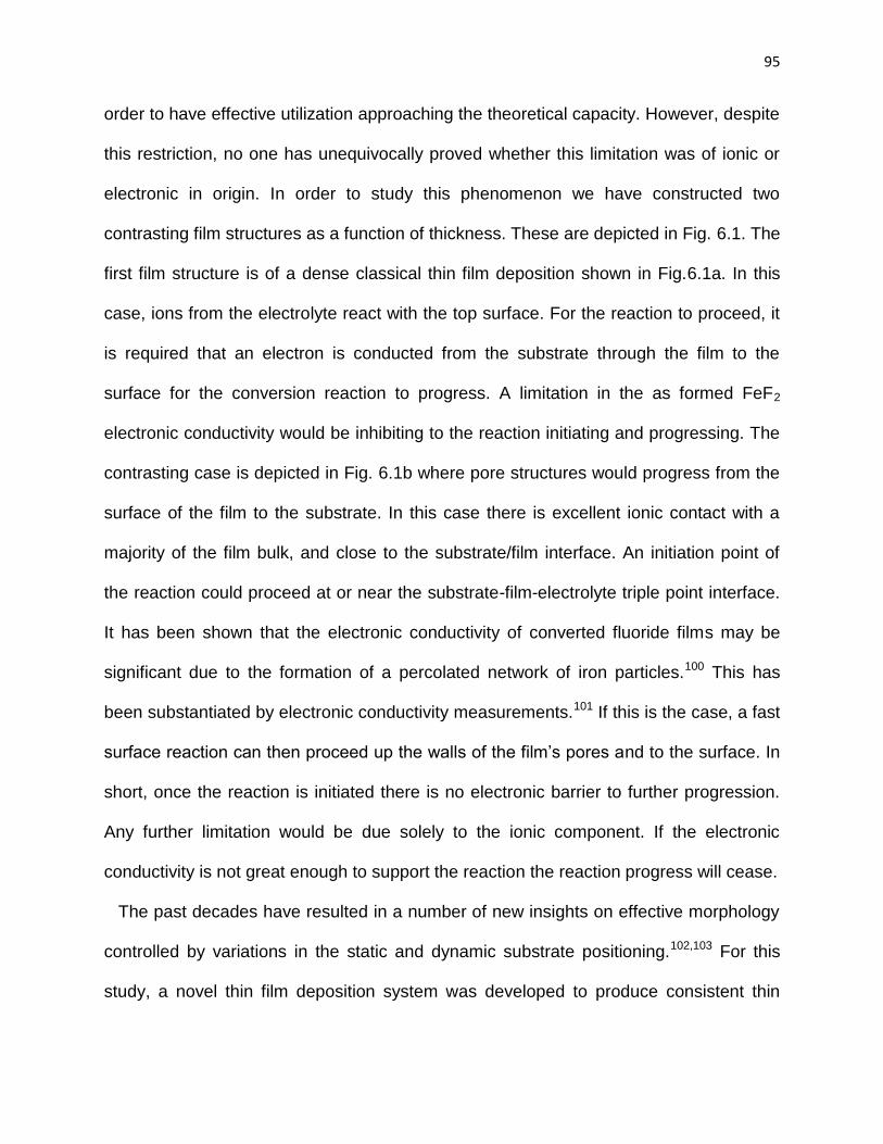
95
order to have effective utilization approaching the theoretical capacity. However, despite
this restriction, no one has unequivocally proved whether this limitation was of ionic or
electronic in origin. In order to study this phenomenon we have constructed two
contrasting film structures as a function of thickness. These are depicted in Fig. 6.1. The
first film structure is of a dense classical thin film deposition shown in Fig.6.1a. In this
case, ions from the electrolyte react with the top surface. For the reaction to proceed, it
is required that an electron is conducted from the substrate through the film to the
surface for the conversion reaction to progress. A limitation in the as formed FeF2
electronic conductivity would be inhibiting to the reaction initiating and progressing. The
contrasting case is depicted in Fig. 6.1b where pore structures would progress from the
surface of the film to the substrate. In this case there is excellent ionic contact with a
majority of the film bulk, and close to the substrate/film interface. An initiation point of
the reaction could proceed at or near the substrate-film-electrolyte triple point interface.
It has been shown that the electronic conductivity of converted fluoride films may be
significant due to the formation of a percolated network of iron particles.100 This has
been substantiated by electronic conductivity measurements.101 If this is the case, a fast
surface reaction can then proceed up the walls of the film’s pores and to the surface. In
short, once the reaction is initiated there is no electronic barrier to further progression.
Any further limitation would be due solely to the ionic component. If the electronic
conductivity is not great enough to support the reaction the reaction progress will cease.
The past decades have resulted in a number of new insights on effective morphology
controlled by variations in the static and dynamic substrate positioning.102,103 For this
study, a novel thin film deposition system was developed to produce consistent thin
96
films of a wide range of thicknesses with unique morphologies which can influence the
film’s interfacial surface area. The system was based on a physical vapor deposition
technique called glancing angle deposition (GLAD) where the morphology of the film
growth can be controlled through substrate rotational positioning at defined oblique
angles to the deposition source.
Figure 6.1: Lithiated film structures (a) classical static film and (b) porous dynamic film
In past literature electrochemistry studies using FeF2 thin film electrodes, the maximum
film thickness was less than 150nm due to the limiting insulating characteristic property
of FeF2.104 In contrast, this study uses films with thicknesses of 850nm produced by the
97
GLAD concept which show improved electrochemical performance relative to classical
statically produced thinner films.
6.2 Experimental
6.2.1 Material Synthesis
The thin films were prepared in a custom fabricated high vacuum electron beam
evaporation chamber. The electron beam evaporator consisted of a MDC 3kW Mighty
Source with four 2cc rotating crucibles. The substrate was mounted approximately
23cm from the e-beam source onto a 76mm diameter drum 178mm in length that is
positional through a programmable logic controlled servo motor (Ormec).
Prior to the deposition the substrate was prepared using unpolished high-
strength aluminium alloy 7075 (McMaster-Carr) with a thickness of 0.8mm. The Al-7075
substrate was cut into a 25mm x 75mm strip with the grains running parallel to the width
of the strip. The Al-7075 strip was cleaned with acetone then methanol and placed in
the center of a flat substrate holding plate along with two cleaned glass microscope
slides 25mm x 75mm with a thickness of 1mm. The glass slides were laid flat and place
on each side of the Al-7075 strip and the three pieces were secured to the substrate
holding plate using Kapton® tape. The glass slides were later used to measure film
thickness.
The source material of approximately 5g total of FeF2 powder (Advanced
Research Chemicals) was packed tightly into three of the four 2cc graphite crucible
liners. The fourth crucible liner was loaded with titanium (99.99% Ti granules, Alfa). The
substrate holder containing the Al-7075 substrate and glass slides was bolted to the
76mm diameter programmable drum with the length of the strips running parallel to the
98
length of the drum. The vacuum chamber was then brought to a pressure of 3x10⁻⁶
Torr.
To provide an adhesion layer for the FeF2, 50nm of titanium was first deposited
onto the substrate in the Static 0° angle position. During the deposition of titanium a
voltage of 4.8kV with a current of 80mA were applied and the deposition rate was
approximately 10A°/sec. Next, FeF2 was deposited with a voltage of 4.8kV with a
current of 5mA and the deposition rate was approximately 13A°/sec. Once the
deposition was completed, the chamber was vented with a combination of nitrogen then
dry air. The films were removed from chamber and then stored in a helium filled
glovebox (<0.6 ppm H2O, <0.1 ppm O2) until coin cell fabrication and characterization
trials. Prior to cell fabrication and in room atmosphere, 14.3mm discs were punched
from the film to create electrodes.
Fig. 6.2 shows schematics comparing the static verse dynamic depositions. For
the static deposition, the substrate holder was bolted to the drum in an orientation that
was parallel to the base of the chamber which was referenced to be a 0° angle. During
the static deposition, the substrate position was held constant at a 0° angle. The
dynamic deposition consisted of rotating the programmable substrate drum at various
angles and rotations per minute (rpm) depending on the specific deposition. For
example, during the 48°-52° deposition the 50nm titanium adhesion layer was first
deposited statically at a 0° angle. Second, the substrate was rotated counter clockwise
(CCW) to an angle of 48° prior to depositing FeF2. Third, the FeF2 deposition
evaporation flux was started. Next, the program rotated the substrate drum in the
following sequence; CCW at 0.65rpm through 48° to 52°, CCW at 26rpm through 52° to
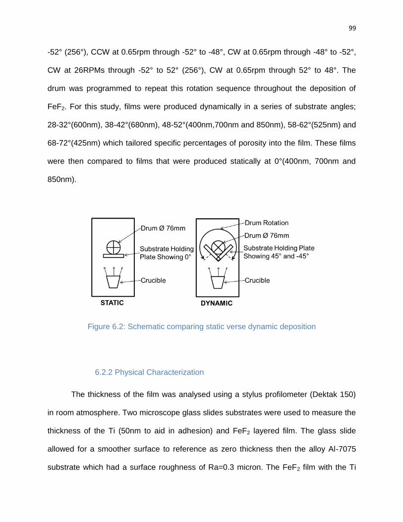
99
-52° (256°), CCW at 0.65rpm through -52° to -48°, CW at 0.65rpm through -48° to -52°,
CW at 26RPMs through -52° to 52° (256°), CW at 0.65rpm through 52° to 48°. The
drum was programmed to repeat this rotation sequence throughout the deposition of
FeF2. For this study, films were produced dynamically in a series of substrate angles;
28-32°(600nm), 38-42°(680nm), 48-52°(400nm,700nm and 850nm), 58-62°(525nm) and
68-72°(425nm) which tailored specific percentages of porosity into the film. These films
were then compared to films that were produced statically at 0°(400nm, 700nm and
850nm).
Figure 6.2: Schematic comparing static verse dynamic deposition
6.2.2 Physical Characterization
The thickness of the film was analysed using a stylus profilometer (Dektak 150)
in room atmosphere. Two microscope glass slides substrates were used to measure the
thickness of the Ti (50nm to aid in adhesion) and FeF2 layered film. The glass slide
allowed for a smoother surface to reference as zero thickness then the alloy Al-7075
substrate which had a surface roughness of Ra=0.3 micron. The FeF2 film with the Ti
100
adhesion layer on the glass substrates were measured in four locations and an average
thickness was calculated. The average film thickness was then subtracted by 50nm, the
titanium adhesion layer, to determine the FeF2 film thickness.
X-ray Diffraction (XRD) (Bruker) using CuKα radiation was performed to the films
to understand the crystallographic orientation. A dedicated 10mm x 10mm piece of film
was used for the XRD analysis in room atmosphere. The crystallite size was derived by
the Scherrer method. XRD data was processed through the use of Topas software .
FeF2 films were analyzed with a Field Emission Scanning Electron Microscopy
(FESEM) (Zeiss). The films were exposed for approximately 2 minutes to room air while
being mounted in the FESEM.
Image-J, an imaging processing and analysis Java based software (National
Institute of Health, USA) was used to modify the FESEM images into binary images to
calculate the canyon facial porosity percentage and the perimeter length of each
canyon. The facial porosity percentage results were used to correct the mass of the film
for electrochemical characterization.
6.1.3 Electrochemical Characterization
All batteries fabricated for studies in this paper were fabricated in aluminized (on
the positive electrode) 2032 coin cells (Hosen) made with cathodes consisting of a 14.3
mm diameter disc of iron fluoride film on Al-7075 substrate, two layers of borosilicate
glass fiber separator (Whatman) with a diameter of 15.9 mm soaked with electrolyte,
and a 0.3mm thick 12.7mm diameter lithium metal foil as the anode counter electrode
(half-cell) (FMC). The electrolyte was 1 M LiPF6 EC: DMC (Novolyte), stored in a helium
filled glovebox and used without additional treatment. Galvanostatic cycling tests were
101
performed in a dry room on a MacPile II (Biologic). The cells were cycled
galvanostatically between 4.50 V and 1.00 V at a constant current of 12.5 mA g-1 in an
oven set at 60oC.
6.3 Results
6.3.1 Crystallography
XRD was performed on the films to understand the effect of deposition
conditions, on crystallographic orientation, crystallite size and lattice parameters. The
films were scanned over the 2θ ranges of 20-37° and 48-65° to avoid the intense
reflection from the Al substrate. Fig. 6.3a shows the scans of FeF2 films produced
dynamically in a series of substrate angles, 28-32°(600nm), 38-42°(680nm), 58-
62°(525nm) and 68-72°(425nm). Fig. 6.3b shows the scans of films produced
dynamically at a substrate angle of 48-52° and systematically increased thicknesses of
400nm, 700nm and 850nm. Fig. 6.3c shows the scans of the films produced statically
at a substrate angle of 0° with similar thicknesses to those obtained dynamically at 48-
52°. Diffraction reveals that all films are composed of single crystalline phase FeF2 of
rutile structure with the exception of the film obtained dynamically at the substrate angle
of 68-72° scan that revealed very poor crystallization. Lattice parameters in Table 1 are
fairly consistent with ICDD values of a=4.70Å and c=3.31Å showing some compression
in the c parameter.
Molecular dynamics simulations have previously shown that the Li+ diffusion
barrier along the [110] channel is approximately 70% greater than the barrier along the
[001] channel.105 To understand if the films had preferred crystallographic orientation.
102
that could directly impact electrochemical performance, the integrated intensity ratios of
the (110) and (211) reflections were calculated and summarized in Table 1. The
(110)/(211) peak area ratios show dependence on the deposition angle. The (110)/(211)
ratio was found to decrease as the thickness increased. As reference, the calculated
peak area ratio for the macroscopic phase pure FeF2 powder was 2.44 suggesting
texturing in the preferred <110> for the films. It is important to note that the (110) and
(211) peak area ratio is drastically increased with the titanium adhesion layer verse
without. All films used in this study comprised a titanium adhesion layer.
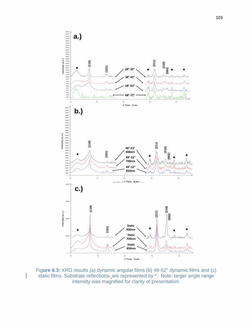
103
Figure 6.3: XRD results (a) dynamic angular films (b) 48-52° dynamic films and (c) static films. Substrate reflections are represented by *. Note: larger angle range
intensity was magnified for clarity of presentation.
5248 400 2037
Operations: Y Scale Add 1000 | Y Scale Norm 4.045 | Background 0.000,1.000 | Fourier 5.000 x
5248 850 4865 - File: 5248_850nm_4865.raw - Type: Locked Coupled - Start: 48.000 ° - End: 6
Operations: Y Scale Add 1000 | Background 0.000,1.000 | Fourier 5.000 x 1 | Strip kAlpha2 0.50
5248 850 2037 - File: 5248_850nm_2037.raw - Type: Locked Coupled - Start: 20.000 ° - End: 3
Operations: Y Scale Add 3000 | Y Scale Norm 9.694 | Background 0.000,1.000 | Fourier 5.000 x
5248deg 4865 - File: 5248_700nm_4865.raw - Type: Locked Coupled - Start: 48.000 ° - End: 64
Operations: Y Scale Add 3000 | Y Scale Norm 1.732 | Background 0.000,1.000 | Fourier 5.000 x
5248deg 2037 - File: 5248_700nm_2037.raw - Type: Locked Coupled - Start: 20.000 ° - End: 36
Operations: Y Scale Add 5000 | Y Scale Norm 11.473 | Background 0.000,1.000 | Fourier 5.000
5248 400 4865 - File: 5248_400nm_4865.raw - Type: Locked Coupled - Start: 48.000 ° - End: 6
Operations: Y Scale Add 5000 | Y Scale Norm 2.300 | Background 0.000,1.000 | Fourier 5.000 x
5248 400 2037 - File: 5248_400nm_2037.raw - Type: Locked Coupled - Start: 20.000 ° - End: 3
Lin
(C
ounts
)
0
1000
2000
3000
4000
5000
6000
7000
8000
9000
10000
11000
12000
13000
14000
15000
16000
17000
18000
19000
20000
21000
22000
23000
24000
25000
26000
27000
2-Theta - Scale
20 30 40 50 60
48°-52°400nm
48°-52°700nm
48°-52°850nm
b.)
static 400 2037
Operations: Y Scale Add 1000 | Y Scale Norm 4.455 | Background 0.000,1.000 | Fourier 5.000 x
static 1000 4865 - File: Static_1000nm_4865.raw - Type: Locked Coupled - Start: 48.000 ° - End
Operations: Y Scale Add 1000 | Y Scale Norm 1.067 | Background 0.000,1.000 | Fourier 5.000 x
static 1000 2037 - File: Static_1000nm_2037.raw - Type: Locked Coupled - Start: 20.000 ° - End
Operations: Y Scale Add 3000 | Y Scale Norm 7.307 | Background 0.000,1.000 | Fourier 5.000 x
static 700 4865 - File: Static_700nm_4865.raw - Type: Locked Coupled - Start: 48.000 ° - End: 6
Operations: Y Scale Add 3000 | Y Scale Norm 1.794 | Background 0.000,1.000 | Fourier 5.000 x
static 700 2037 - File: Static_700nm_2037.raw - Type: Locked Coupled - Start: 20.000 ° - End: 3
Operations: Y Scale Add 2000 | Y Scale Add 2000 | Y Scale Add 5000 | Y Scale Norm 9.255 | B
static 400 4865 - File: Static_400nm_4865.raw - Type: Locked Coupled - Start: 48.000 ° - End: 6
Operations: Y Scale Add 2000 | Y Scale Add 2000 | Y Scale Add 5000 | Background 0.000,1.00
static 400 2037 - File: Static_400nm_2037.raw - Type: Locked Coupled - Start: 20.000 ° - End: 3
Lin
(C
ou
nts
)
0
10000
20000
30000
40000
2-Theta - Scale
20 30 40 50 60
Static400nm
Static700nm
Static850nm
c.)
3228deg 48-65
Operations: Y Scale Add 1000 | Y Scale Norm 17.671 | Background 0.000,1.000 | Fourier 5.000
7268 4865 - File: 7268_4865.raw - Type: Locked Coupled - Start: 48.000 ° - End: 64.999 ° - Ste
Operations: Y Scale Add 1000 | Y Scale Add -100 | Y Scale Add 100 | Y Scale Norm 5.044 | Ba
7268 2037 - File: 7268_2037.raw - Type: Locked Coupled - Start: 20.000 ° - End: 36.999 ° - Ste
Operations: Y Scale Add -1000 | Y Scale Add 5000 | Y Scale Norm 7.998 | Background 0.000,1.
6258 4865 - File: 6258_4865.raw - Type: Locked Coupled - Start: 48.000 ° - End: 64.999 ° - Ste
Operations: Y Scale Add -1000 | Y Scale Add 5000 | Y Scale Norm 1.367 | Background 0.000,1.
6258 2037 - File: 6258_2037.raw - Type: Locked Coupled - Start: 20.000 ° - End: 36.999 ° - Ste
Operations: Y Scale Add -1000 | Y Scale Add -2000 | Y Scale Add 10000 | Y Scale Norm 5.292
4238_4865 - File: 4238_4865 12-20-12.raw - Type: Locked Coupled - Start: 48.000 ° - End: 64.9
Operations: Y Scale Add 1000 | Y Scale Add -2000 | Y Scale Add -2000 | Y Scale Add 10000 |
4238_2037 - File: 4238_2037 12-20-12.raw - Type: Locked Coupled - Start: 20.000 ° - End: 36.9
Operations: Y Scale Add -2000 | Y Scale Add 12000 | Y Scale Norm 1.765 | Background 0.000,
3228deg 20-37 - File: 3228deg 2037.raw - Type: Locked Coupled - Start: 20.000 ° - End: 36.999
Operations: Y Scale Add -2000 | Y Scale Add 12000 | Y Scale Norm 4.319 | Background 0.000,
3228deg 48-65 - File: 3228_4865.raw - Type: Locked Coupled - Start: 48.000 ° - End: 64.999 ° -
Lin
(C
oun
ts)
0
1000
2000
3000
4000
5000
6000
7000
8000
9000
10000
11000
12000
13000
14000
15000
16000
17000
18000
19000
20000
21000
22000
23000
24000
25000
26000
27000
28000
29000
30000
2-Theta - Scale
20 30 40 50 60
28°-32°
38°-42°
58°-62°
68°-72°
a.)
(11
0)
(21
1)
(10
1) (21
0)
(00
2)
** **
Inte
nsity (
a.u
.)
Inte
nsity (
a.u
.)
Inte
nsity (
a.u
.)
(11
0)
(21
1)
(10
1)
(21
0)
(00
2)
** **
(11
0)
(21
1)
(10
1)
(21
0)
(00
2)
** **
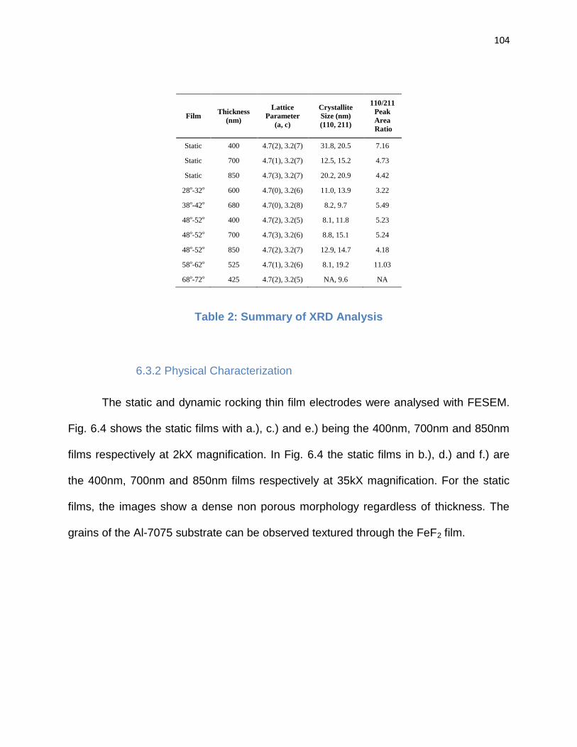
104
Film Thickness
(nm)
Lattice
Parameter
(a, c)
Crystallite
Size (nm)
(110, 211)
110/211
Peak
Area
Ratio
Static 400 4.7(2), 3.2(7) 31.8, 20.5 7.16
Static 700 4.7(1), 3.2(7) 12.5, 15.2 4.73
Static 850 4.7(3), 3.2(7) 20.2, 20.9 4.42
28o-32o 600 4.7(0), 3.2(6) 11.0, 13.9 3.22
38o-42o 680 4.7(0), 3.2(8) 8.2, 9.7 5.49
48o-52o 400 4.7(2), 3.2(5) 8.1, 11.8 5.23
48o-52o 700 4.7(3), 3.2(6) 8.8, 15.1 5.24
48o-52o 850 4.7(2), 3.2(7) 12.9, 14.7 4.18
58o-62o 525 4.7(1), 3.2(6) 8.1, 19.2 11.03
68o-72o 425 4.7(2), 3.2(5) NA, 9.6 NA
Table 2: Summary of XRD Analysis
6.3.2 Physical Characterization
The static and dynamic rocking thin film electrodes were analysed with FESEM.
Fig. 6.4 shows the static films with a.), c.) and e.) being the 400nm, 700nm and 850nm
films respectively at 2kX magnification. In Fig. 6.4 the static films in b.), d.) and f.) are
the 400nm, 700nm and 850nm films respectively at 35kX magnification. For the static
films, the images show a dense non porous morphology regardless of thickness. The
grains of the Al-7075 substrate can be observed textured through the FeF2 film.
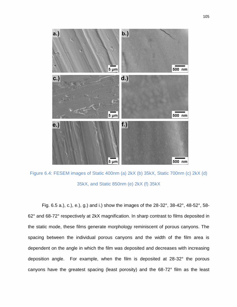
105
Figure 6.4: FESEM images of Static 400nm (a) 2kX (b) 35kX, Static 700nm (c) 2kX (d)
35kX, and Static 850nm (e) 2kX (f) 35kX
Fig. 6.5 a.), c.), e.), g.) and i.) show the images of the 28-32°, 38-42°, 48-52°, 58-
62° and 68-72° respectively at 2kX magnification. In sharp contrast to films deposited in
the static mode, these films generate morphology reminiscent of porous canyons. The
spacing between the individual porous canyons and the width of the film area is
dependent on the angle in which the film was deposited and decreases with increasing
deposition angle. For example, when the film is deposited at 28-32° the porous
canyons have the greatest spacing (least porosity) and the 68-72° film as the least

106
spacing (greatest porosity). This can be observed in more detail in Fig. 6.5 b.), d.), f.),
h.) and j.) which show the images of the 28-32°, 38-42°, 48-52°, 58-62° and 68-72°
respectively at 35kX magnification. These images reconfirm the morphology of the film
is one of porous canyons that have a tiger stripe like appearance when viewed
perpendicular from the face of the surface. The width of the pore ranges from
approximately 50-150nm depending on the deposition angle in which the film was
produced.
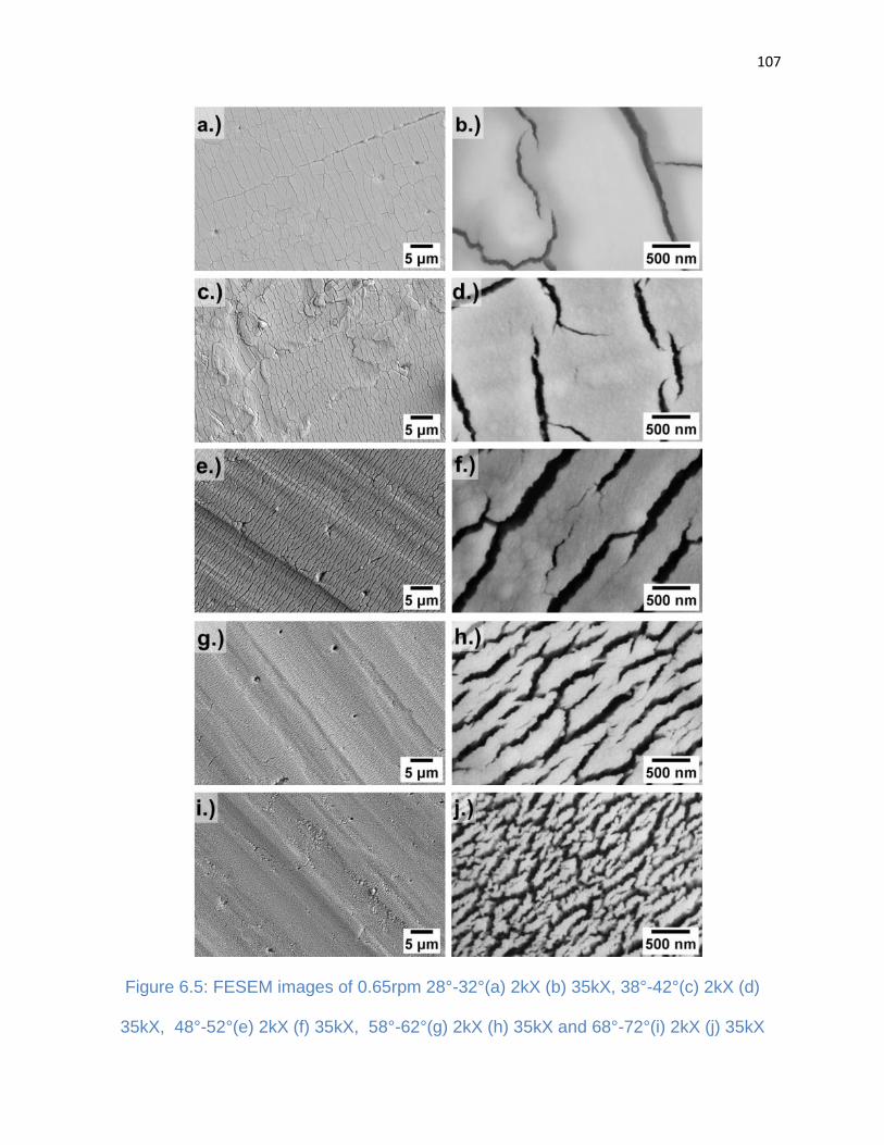
107
Figure 6.5: FESEM images of 0.65rpm 28°-32°(a) 2kX (b) 35kX, 38°-42°(c) 2kX (d)
35kX, 48°-52°(e) 2kX (f) 35kX, 58°-62°(g) 2kX (h) 35kX and 68°-72°(i) 2kX (j) 35kX
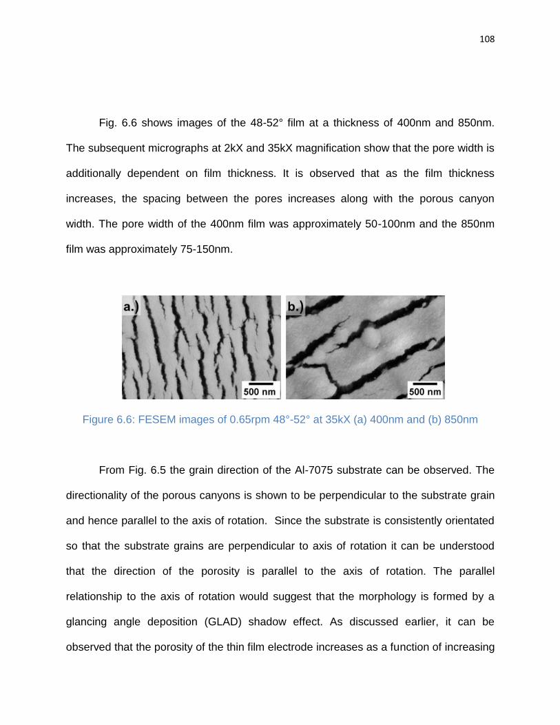
108
Fig. 6.6 shows images of the 48-52° film at a thickness of 400nm and 850nm.
The subsequent micrographs at 2kX and 35kX magnification show that the pore width is
additionally dependent on film thickness. It is observed that as the film thickness
increases, the spacing between the pores increases along with the porous canyon
width. The pore width of the 400nm film was approximately 50-100nm and the 850nm
film was approximately 75-150nm.
Figure 6.6: FESEM images of 0.65rpm 48°-52° at 35kX (a) 400nm and (b) 850nm
From Fig. 6.5 the grain direction of the Al-7075 substrate can be observed. The
directionality of the porous canyons is shown to be perpendicular to the substrate grain
and hence parallel to the axis of rotation. Since the substrate is consistently orientated
so that the substrate grains are perpendicular to axis of rotation it can be understood
that the direction of the porosity is parallel to the axis of rotation. The parallel
relationship to the axis of rotation would suggest that the morphology is formed by a
glancing angle deposition (GLAD) shadow effect. As discussed earlier, it can be
observed that the porosity of the thin film electrode increases as a function of increasing

109
substrate deposition angle. This angular dependence of the porosity is indicative of
traditional glancing angle deposition.
To further understand how the morphology is dependent on the rotation velocity
and angle positioning of the substrate, additional dynamic rocking depositions and their
respective FESEM images were completed. Fig. 6.7a, 6.7b and 6.7c show images of a
60°-80°, 40°-60° and 40°-80° films respectively. These films were rotated in the same
method that was previously explained in Fig. 6.2 and similar to the films produced at
0.65rpms and shown in Fig. 6.5 and Fig. 6.6. However, these films were rotated at a
velocity of 6.5rpm (replacing the 0.65rpm of the films previously discussed) through
these concentrated angles and then rotated at 26rpm through all other angles. The films
show a similar porosity trend as the 0.65rpm films with increasing porosity as the angle
is increased.
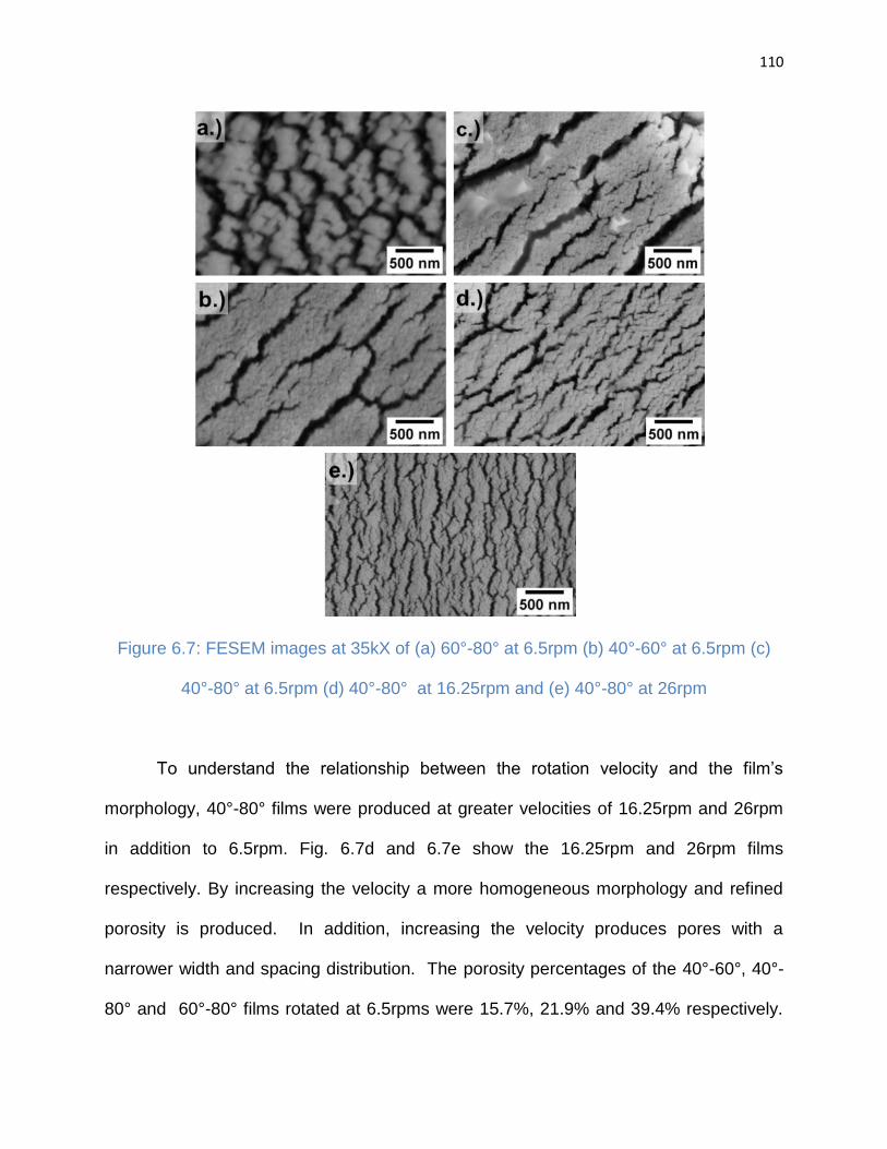
110
Figure 6.7: FESEM images at 35kX of (a) 60°-80° at 6.5rpm (b) 40°-60° at 6.5rpm (c)
40°-80° at 6.5rpm (d) 40°-80° at 16.25rpm and (e) 40°-80° at 26rpm
To understand the relationship between the rotation velocity and the film’s
morphology, 40°-80° films were produced at greater velocities of 16.25rpm and 26rpm
in addition to 6.5rpm. Fig. 6.7d and 6.7e show the 16.25rpm and 26rpm films
respectively. By increasing the velocity a more homogeneous morphology and refined
porosity is produced. In addition, increasing the velocity produces pores with a
narrower width and spacing distribution. The porosity percentages of the 40°-60°, 40°-
80° and 60°-80° films rotated at 6.5rpms were 15.7%, 21.9% and 39.4% respectively.

111
The porosity percentage of the 40°-80° film rotated at 6.5rpm, 16.25rpm and 26rpm
were 21.9%, 27.5% and 32.1% respectively suggesting that an increase in velocity
systematically increases the porosity.
6.3.3 Quantitative Micro/Nanostructure
Image processing was used to calculate the canyon facial porosity percentage
and the perimeter length of each canyon. The FESEM images were modified into binary
images. The results of the binary images for the dynamic depositions 28-32°, 38-42°,
48-52°, 58-62° and 68-72° are shown in Fig. 6.8. The results of the binary images for
the static depositions 0° (400nm, 700nm and 850nm) are shown in Fig. 6.9.
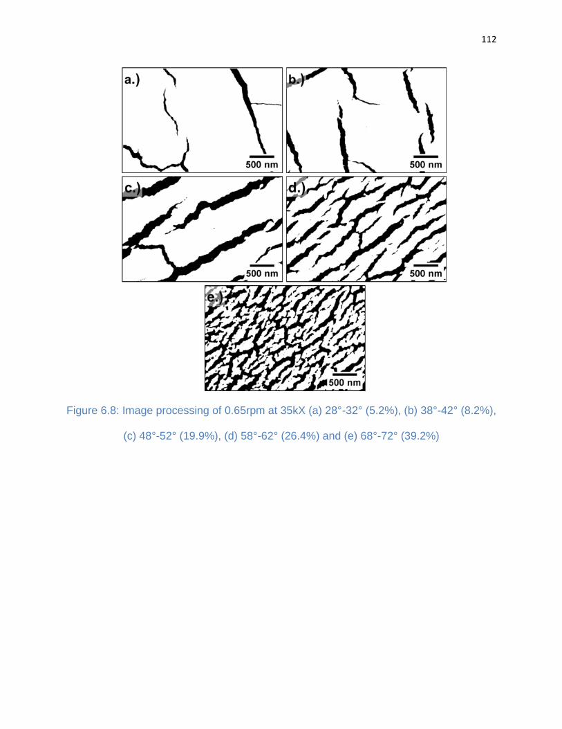
112
Figure 6.8: Image processing of 0.65rpm at 35kX (a) 28°-32° (5.2%), (b) 38°-42° (8.2%),
(c) 48°-52° (19.9%), (d) 58°-62° (26.4%) and (e) 68°-72° (39.2%)
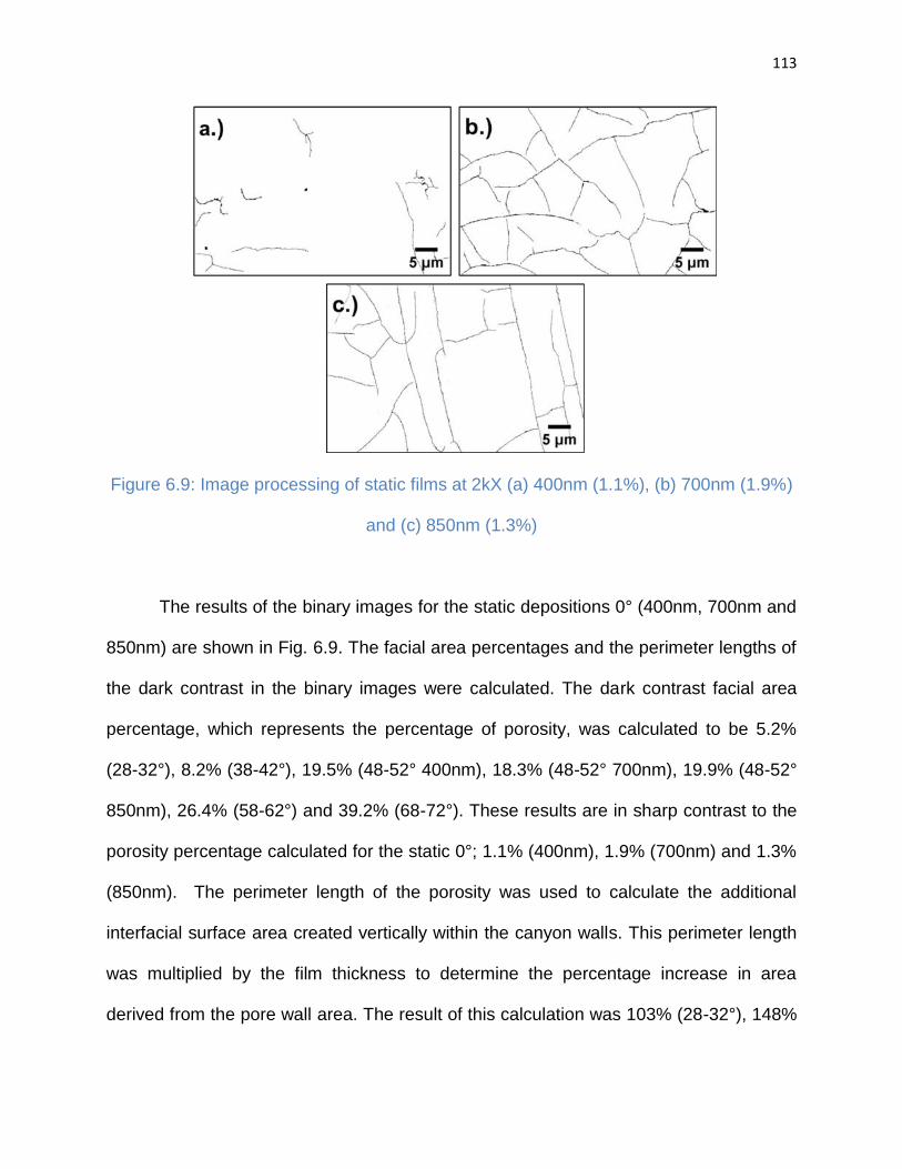
113
Figure 6.9: Image processing of static films at 2kX (a) 400nm (1.1%), (b) 700nm (1.9%)
and (c) 850nm (1.3%)
The results of the binary images for the static depositions 0° (400nm, 700nm and
850nm) are shown in Fig. 6.9. The facial area percentages and the perimeter lengths of
the dark contrast in the binary images were calculated. The dark contrast facial area
percentage, which represents the percentage of porosity, was calculated to be 5.2%
(28-32°), 8.2% (38-42°), 19.5% (48-52° 400nm), 18.3% (48-52° 700nm), 19.9% (48-52°
850nm), 26.4% (58-62°) and 39.2% (68-72°). These results are in sharp contrast to the
porosity percentage calculated for the static 0°; 1.1% (400nm), 1.9% (700nm) and 1.3%
(850nm). The perimeter length of the porosity was used to calculate the additional
interfacial surface area created vertically within the canyon walls. This perimeter length
was multiplied by the film thickness to determine the percentage increase in area
derived from the pore wall area. The result of this calculation was 103% (28-32°), 148%
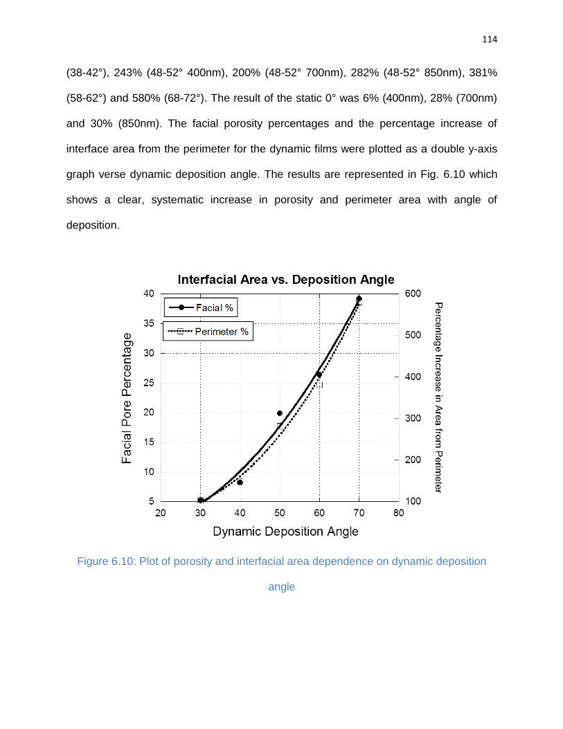
114
(38-42°), 243% (48-52° 400nm), 200% (48-52° 700nm), 282% (48-52° 850nm), 381%
(58-62°) and 580% (68-72°). The result of the static 0° was 6% (400nm), 28% (700nm)
and 30% (850nm). The facial porosity percentages and the percentage increase of
interface area from the perimeter for the dynamic films were plotted as a double y-axis
graph verse dynamic deposition angle. The results are represented in Fig. 6.10 which
shows a clear, systematic increase in porosity and perimeter area with angle of
deposition.
Figure 6.10: Plot of porosity and interfacial area dependence on dynamic deposition
angle
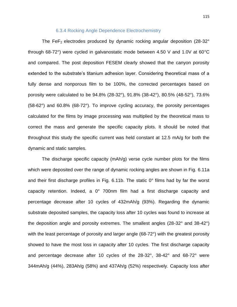
115
6.3.4 Rocking Angle Dependence Electrochemistry
The FeF2 electrodes produced by dynamic rocking angular deposition (28-32°
through 68-72°) were cycled in galvanostatic mode between 4.50 V and 1.0V at 60°C
and compared. The post deposition FESEM clearly showed that the canyon porosity
extended to the substrate’s titanium adhesion layer. Considering theoretical mass of a
fully dense and nonporous film to be 100%, the corrected percentages based on
porosity were calculated to be 94.8% (28-32°), 91.8% (38-42°), 80.5% (48-52°), 73.6%
(58-62°) and 60.8% (68-72°). To improve cycling accuracy, the porosity percentages
calculated for the films by image processing was multiplied by the theoretical mass to
correct the mass and generate the specific capacity plots. It should be noted that
throughout this study the specific current was held constant at 12.5 mA/g for both the
dynamic and static samples.
The discharge specific capacity (mAh/g) verse cycle number plots for the films
which were deposited over the range of dynamic rocking angles are shown in Fig. 6.11a
and their first discharge profiles in Fig. 6.11b. The static 0° films had by far the worst
capacity retention. Indeed, a 0° 700nm film had a first discharge capacity and
percentage decrease after 10 cycles of 432mAh/g (93%). Regarding the dynamic
substrate deposited samples, the capacity loss after 10 cycles was found to increase at
the deposition angle and porosity extremes. The smallest angles (28-32° and 38-42°)
with the least percentage of porosity and larger angle (68-72°) with the greatest porosity
showed to have the most loss in capacity after 10 cycles. The first discharge capacity
and percentage decrease after 10 cycles of the 28-32°, 38-42° and 68-72° were
344mAh/g (44%), 283Ah/g (58%) and 437Ah/g (52%) respectively. Capacity loss after

116
10 cycles improved for the mid-range deposition angles (48-52° and 58-62°) with a
corresponding first discharge capacity and percentage decrease of 406mAh/g (21%)
and 314mAh/g (12%) respectively. A summary of these results are shown in Fig. 6.12
where the perimeter area porosity percentages and the capacity loss for the dynamic
films were plotted as a double y-axis graph verse dynamic deposition angle.
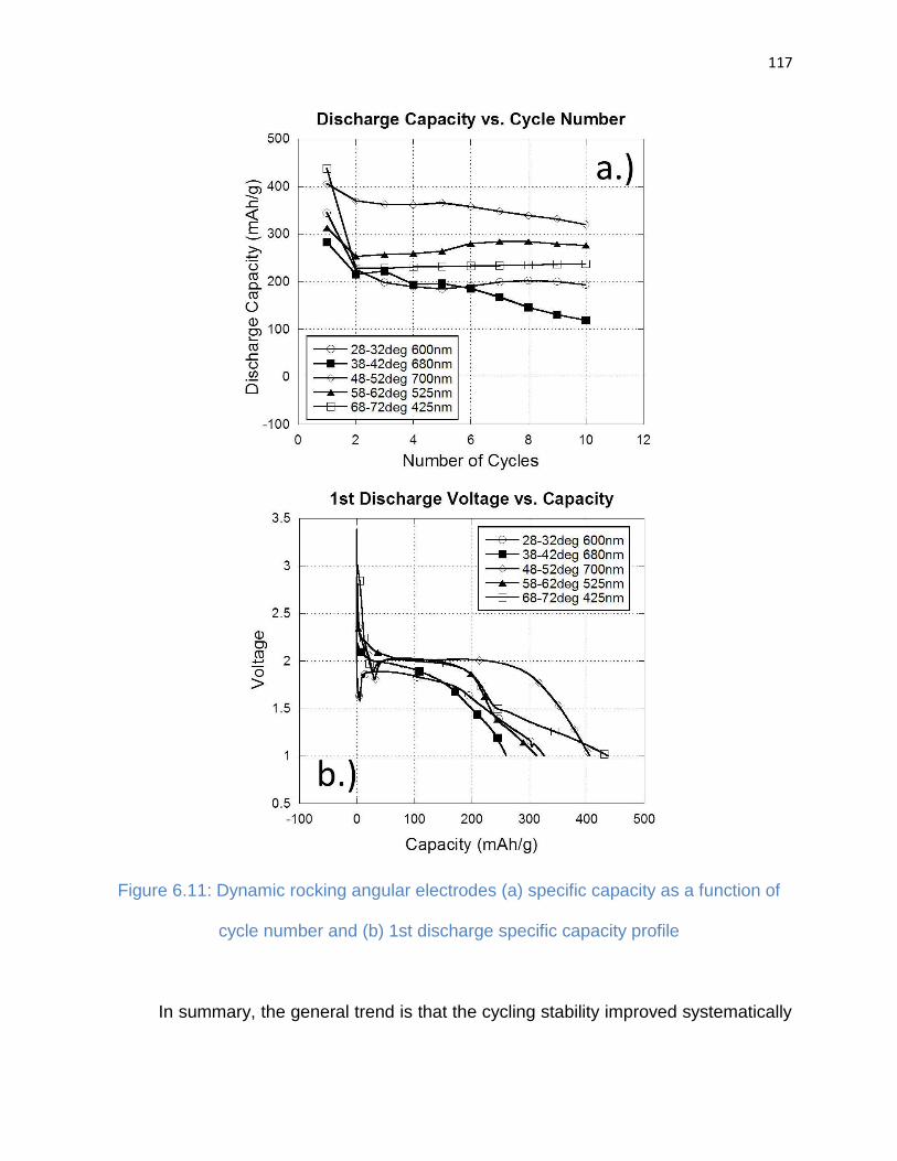
117
Figure 6.11: Dynamic rocking angular electrodes (a) specific capacity as a function of
cycle number and (b) 1st discharge specific capacity profile
In summary, the general trend is that the cycling stability improved systematically
118
with the porosity generated (i.e. higher angles are associated with higher porosity)
especially in contrast to the dense static film which will be discussed in more detail in
the proceeding section. This trend abruptly drops off at 68-72° suggesting another
mechanism of failure may be generated. This could range from poor interconnection
amongst the grains due to the high porosity leading to accelerated de-adhesion from the
substrate while cycling from mechanical forces, breakdown of lateral electronic
percolation, enhancement of deleterious aspects of electrolyte interaction, or significant
change in crystallography previously noted for this film deposition angle.
Figure 6.12: Influence of dynamic deposition angle on perimeter surface area and
capacity
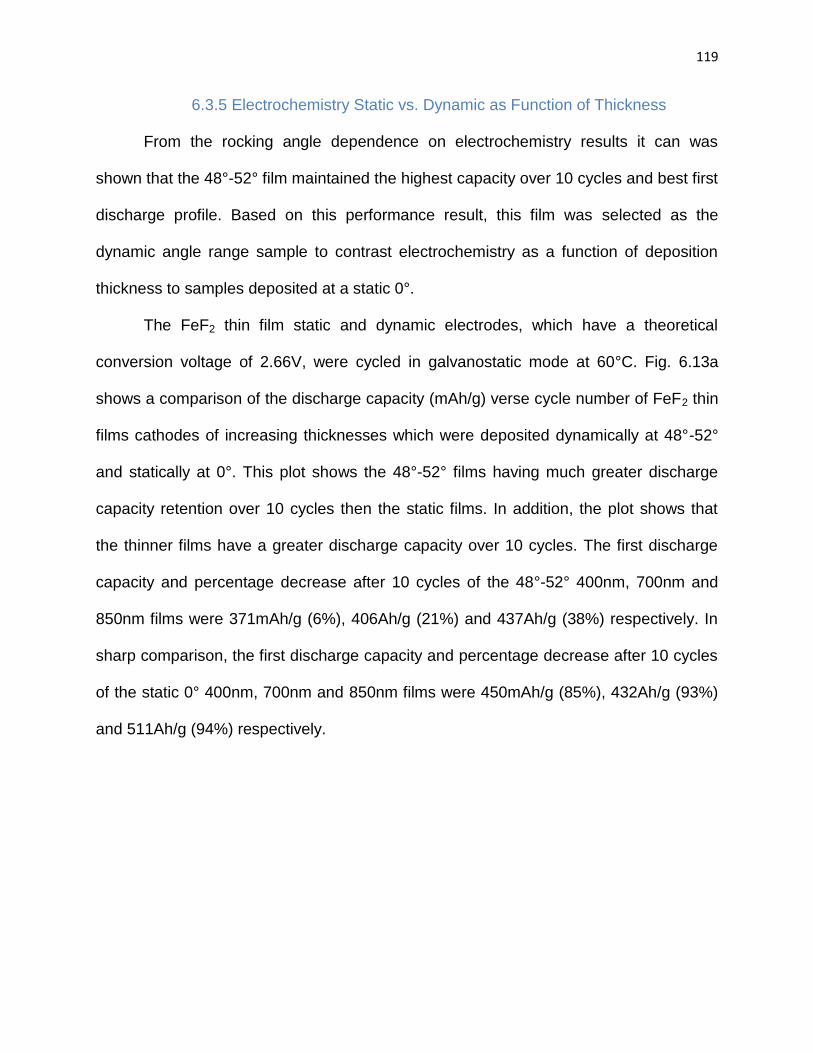
119
6.3.5 Electrochemistry Static vs. Dynamic as Function of Thickness
From the rocking angle dependence on electrochemistry results it can was
shown that the 48°-52° film maintained the highest capacity over 10 cycles and best first
discharge profile. Based on this performance result, this film was selected as the
dynamic angle range sample to contrast electrochemistry as a function of deposition
thickness to samples deposited at a static 0°.
The FeF2 thin film static and dynamic electrodes, which have a theoretical
conversion voltage of 2.66V, were cycled in galvanostatic mode at 60°C. Fig. 6.13a
shows a comparison of the discharge capacity (mAh/g) verse cycle number of FeF2 thin
films cathodes of increasing thicknesses which were deposited dynamically at 48°-52°
and statically at 0°. This plot shows the 48°-52° films having much greater discharge
capacity retention over 10 cycles then the static films. In addition, the plot shows that
the thinner films have a greater discharge capacity over 10 cycles. The first discharge
capacity and percentage decrease after 10 cycles of the 48°-52° 400nm, 700nm and
850nm films were 371mAh/g (6%), 406Ah/g (21%) and 437Ah/g (38%) respectively. In
sharp comparison, the first discharge capacity and percentage decrease after 10 cycles
of the static 0° 400nm, 700nm and 850nm films were 450mAh/g (85%), 432Ah/g (93%)
and 511Ah/g (94%) respectively.
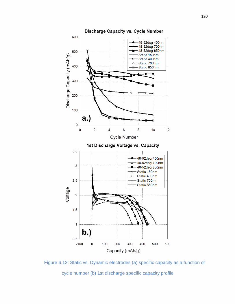
120
Figure 6.13: Static vs. Dynamic electrodes (a) specific capacity as a function of
cycle number (b) 1st discharge specific capacity profile
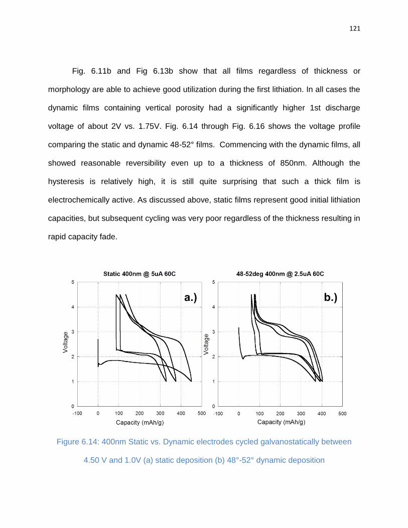
121
Fig. 6.11b and Fig 6.13b show that all films regardless of thickness or
morphology are able to achieve good utilization during the first lithiation. In all cases the
dynamic films containing vertical porosity had a significantly higher 1st discharge
voltage of about 2V vs. 1.75V. Fig. 6.14 through Fig. 6.16 shows the voltage profile
comparing the static and dynamic 48-52° films. Commencing with the dynamic films, all
showed reasonable reversibility even up to a thickness of 850nm. Although the
hysteresis is relatively high, it is still quite surprising that such a thick film is
electrochemically active. As discussed above, static films represent good initial lithiation
capacities, but subsequent cycling was very poor regardless of the thickness resulting in
rapid capacity fade.
Figure 6.14: 400nm Static vs. Dynamic electrodes cycled galvanostatically between
4.50 V and 1.0V (a) static deposition (b) 48°-52° dynamic deposition
122
.
Figure 6.15: 700nm Static vs. Dynamic electrodes cycled galvanostatically between
4.50 V and 1.0V (a) static deposition (b) 48°-52° dynamic deposition.
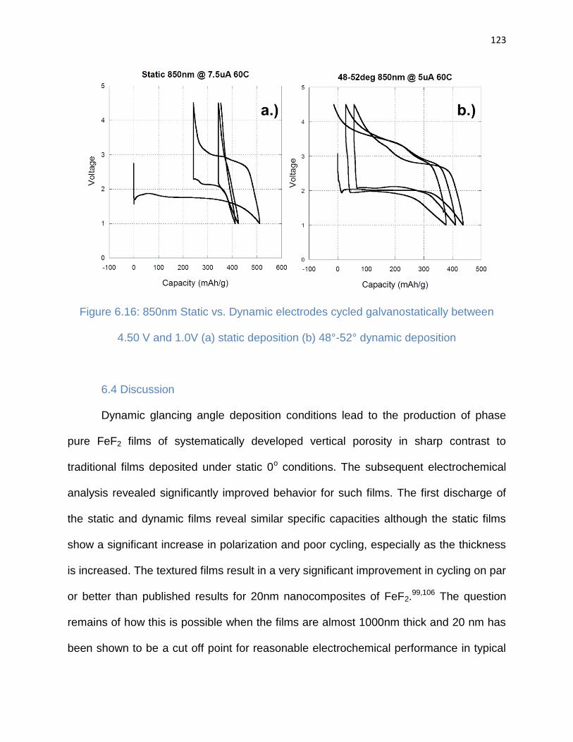
123
Figure 6.16: 850nm Static vs. Dynamic electrodes cycled galvanostatically between
4.50 V and 1.0V (a) static deposition (b) 48°-52° dynamic deposition
6.4 Discussion
Dynamic glancing angle deposition conditions lead to the production of phase
pure FeF2 films of systematically developed vertical porosity in sharp contrast to
traditional films deposited under static 0o conditions. The subsequent electrochemical
analysis revealed significantly improved behavior for such films. The first discharge of
the static and dynamic films reveal similar specific capacities although the static films
show a significant increase in polarization and poor cycling, especially as the thickness
is increased. The textured films result in a very significant improvement in cycling on par
or better than published results for 20nm nanocomposites of FeF2.99,106 The question
remains of how this is possible when the films are almost 1000nm thick and 20 nm has
been shown to be a cut off point for reasonable electrochemical performance in typical

124
porous electrodes.
The width of the ridge-like structures are <300nm with considerable amount of
vertically aligned mesoporosity. This electrolyte accessible porosity allows surface
interaction with the film leading to known exceptionally fast conversion reaction on the
surface of the FeF2 host.107 As FeF2 is a high bandgap insulator, the conversion
reaction must proceed at the point of electron transfer located at the substrate surface
at the bottom of the vertical porosity (Fig. 6.1). It is known from that the conversion
reaction of FeF2 proceeds with a rapid transport on the surface of material. This occurs
as the Fe that is produced is percolated and produces a perfect metallic conducting web
embedded in the LiF. Consistent with the nature of a surface reaction, the Li diffusion is
minimal and little ionic impedance develops as the Li+ does not need to proceed through
the reaction and into the depths of electrode. From there the conversion can proceed
inward relatively quickly as the columns and ridges of materials are 4x thinner than the
film itself.
The static “dense” film also exhibits full lithiation although the polarization is
much higher. Theoretically, there is no mechanism for the electron to conduct through
the relatively thick 800nm insulating film to initiate the reaction at the ionic interface with
the electrolyte at the surface. It should be reinforced that the surface conversion
reaction is quite fast and can spread an electronically conducting web over the entire
surface; all it takes is an initiation point consisting of an electronic transfer from the
substrate to the FeF2 film in proximity to a Li+ ion source from the electrolyte. In reality,
this does exist even in the static dense films. As shown in Fig. 6.9, static films showed
evidence of an intermittent film crack over a large spacing in excess of 5000nm that
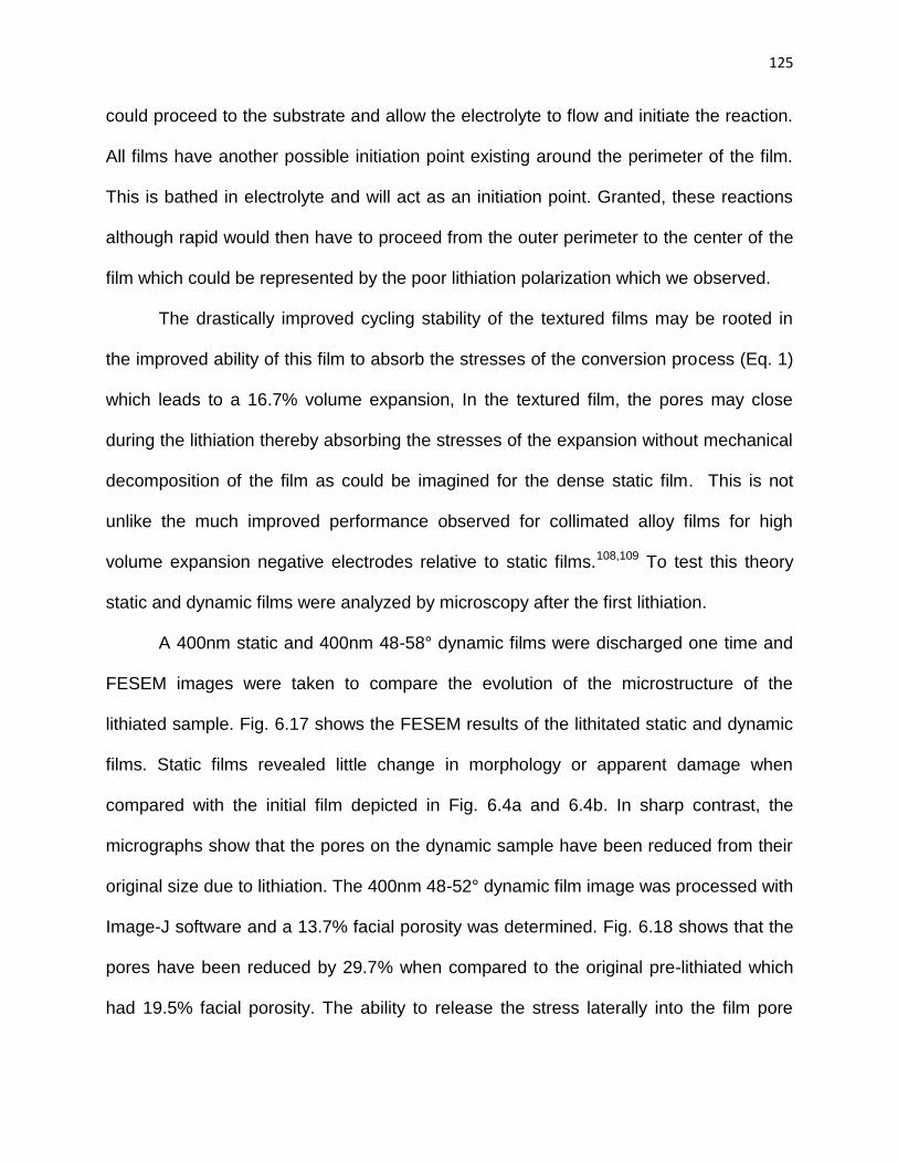
125
could proceed to the substrate and allow the electrolyte to flow and initiate the reaction.
All films have another possible initiation point existing around the perimeter of the film.
This is bathed in electrolyte and will act as an initiation point. Granted, these reactions
although rapid would then have to proceed from the outer perimeter to the center of the
film which could be represented by the poor lithiation polarization which we observed.
The drastically improved cycling stability of the textured films may be rooted in
the improved ability of this film to absorb the stresses of the conversion process (Eq. 1)
which leads to a 16.7% volume expansion, In the textured film, the pores may close
during the lithiation thereby absorbing the stresses of the expansion without mechanical
decomposition of the film as could be imagined for the dense static film. This is not
unlike the much improved performance observed for collimated alloy films for high
volume expansion negative electrodes relative to static films.108,109 To test this theory
static and dynamic films were analyzed by microscopy after the first lithiation.
A 400nm static and 400nm 48-58° dynamic films were discharged one time and
FESEM images were taken to compare the evolution of the microstructure of the
lithiated sample. Fig. 6.17 shows the FESEM results of the lithitated static and dynamic
films. Static films revealed little change in morphology or apparent damage when
compared with the initial film depicted in Fig. 6.4a and 6.4b. In sharp contrast, the
micrographs show that the pores on the dynamic sample have been reduced from their
original size due to lithiation. The 400nm 48-52° dynamic film image was processed with
Image-J software and a 13.7% facial porosity was determined. Fig. 6.18 shows that the
pores have been reduced by 29.7% when compared to the original pre-lithiated which
had 19.5% facial porosity. The ability to release the stress laterally into the film pore
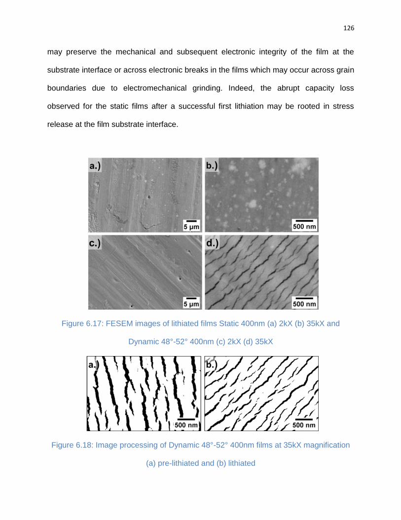
126
may preserve the mechanical and subsequent electronic integrity of the film at the
substrate interface or across electronic breaks in the films which may occur across grain
boundaries due to electromechanical grinding. Indeed, the abrupt capacity loss
observed for the static films after a successful first lithiation may be rooted in stress
release at the film substrate interface.
Figure 6.17: FESEM images of lithiated films Static 400nm (a) 2kX (b) 35kX and
Dynamic 48°-52° 400nm (c) 2kX (d) 35kX
Figure 6.18: Image processing of Dynamic 48°-52° 400nm films at 35kX magnification
(a) pre-lithiated and (b) lithiated
127
6.3.4 LiPON Solid Electrolyte Coated Films
The films were coated with LiPON (lithium phosphorus oxynitride) in an attempt
to better understand the FeF2 reaction mechanism and to determine if possibly the
electrode interaction with the LiPF6 EC: DMC electrolyte leads to accelerating the loss
in cycling capacity. Discussed earlier, in terms of the FeF2 reaction mechanism, initial
Li+ insertion into FeF2 is restricted because Fe2+ reduction is required. For Li+ insertion
to occur some Fe2+ would need to be reduced to either Fe1+ or disproportionation to Fe0
and Fe3+ would need to take place. In general, solid-state Fe1+ is very unlikely and
oxidation states <2+ are uncommon for elements of the first transition series. If some
Fe2+ reduction to Fe0 combines with some Fe2+ oxidation to Fe3+, then metallic iron
would likely precipitate out of the iron fluoride structure.7 In addition, it has been noted
that the metallic nanodomains formed during lithiation of certain conversion materials
can be very catalytic toward the cathodic decomposition of the electrolyte leading to a
film of carbonates on the electrode surface.110 With conversion materials, the solid-
electrolyte interphase (SEI) film may decompose or the metal fluoride may reconvert to
metal oxide or oxyfluoride phases affecting subsequent cycling behavior.111
Once the FeF2 films were fabricated by the ebeam chamber, the LiPON was
applied with a RF sputtering of a Li3PO4 source in nitrogen plasma to create lithium
phosphorus oxynitride (LiPON). The FeF2 electrodes were coated with a 50nm and
100nm thick layer of LiPON. The cells were then fabricated in the same method as with
the cells discussed previously, including the addition of LiPF6 EC: DMC electrolyte
which was placed on top of the LiPON. The electrochemistry cycling results are shown
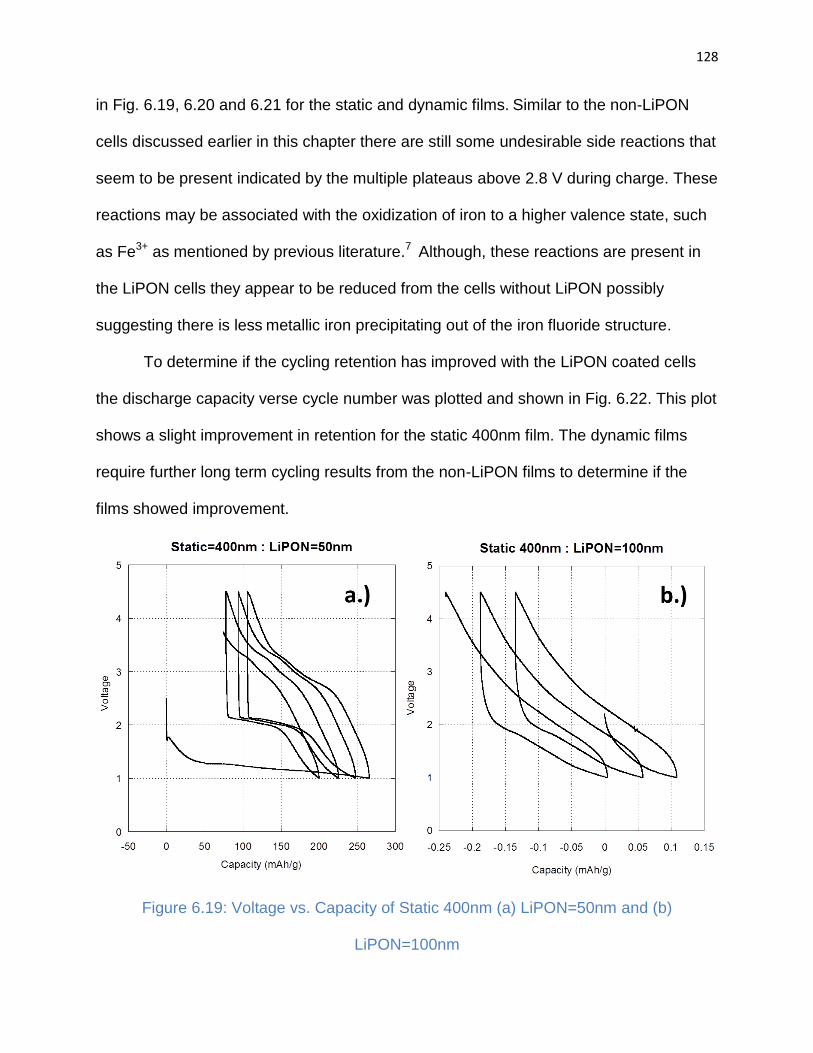
128
in Fig. 6.19, 6.20 and 6.21 for the static and dynamic films. Similar to the non-LiPON
cells discussed earlier in this chapter there are still some undesirable side reactions that
seem to be present indicated by the multiple plateaus above 2.8 V during charge. These
reactions may be associated with the oxidization of iron to a higher valence state, such
as Fe3+ as mentioned by previous literature.7 Although, these reactions are present in
the LiPON cells they appear to be reduced from the cells without LiPON possibly
suggesting there is less metallic iron precipitating out of the iron fluoride structure.
To determine if the cycling retention has improved with the LiPON coated cells
the discharge capacity verse cycle number was plotted and shown in Fig. 6.22. This plot
shows a slight improvement in retention for the static 400nm film. The dynamic films
require further long term cycling results from the non-LiPON films to determine if the
films showed improvement.
Figure 6.19: Voltage vs. Capacity of Static 400nm (a) LiPON=50nm and (b)
LiPON=100nm
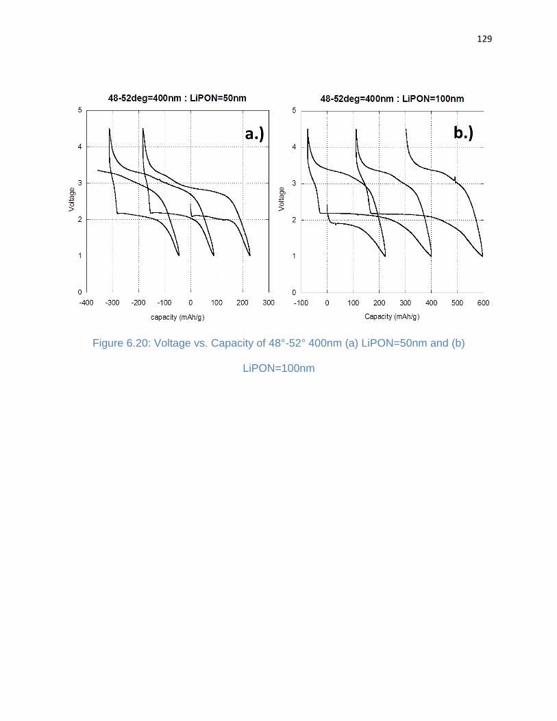
129
Figure 6.20: Voltage vs. Capacity of 48°-52° 400nm (a) LiPON=50nm and (b)
LiPON=100nm
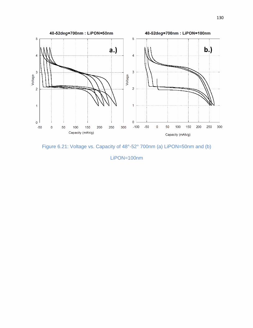
130
Figure 6.21: Voltage vs. Capacity of 48°-52° 700nm (a) LiPON=50nm and (b)
LiPON=100nm
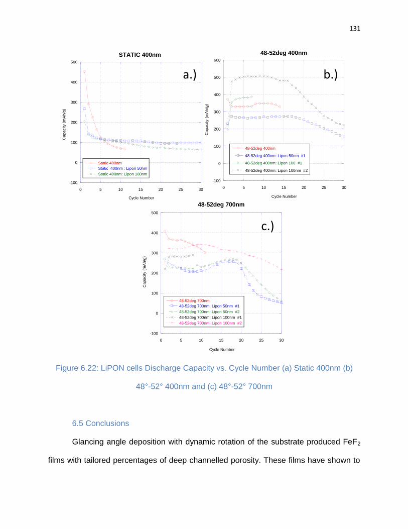
131
Figure 6.22: LiPON cells Discharge Capacity vs. Cycle Number (a) Static 400nm (b)
48°-52° 400nm and (c) 48°-52° 700nm
6.5 Conclusions
Glancing angle deposition with dynamic rotation of the substrate produced FeF2
films with tailored percentages of deep channelled porosity. These films have shown to
-100
0
100
200
300
400
500
0 5 10 15 20 25 30
STATIC 400nm
Static 400nm
Static 400nm : Lipon 50nm
Static 400nm: Lipon 100nm
Cap
acity (
mA
h/g
)
Cycle Number
-100
0
100
200
300
400
500
0 5 10 15 20 25 30
48-52deg 700nm
48-52deg 700nm
48-52deg 700nm: Lipon 50nm #1
48-52deg 700nm: Lipon 50nm #2
48-52deg 700nm: Lipon 100nm #1
48-52deg 700nm: Lipon 100nm #2
Cap
acity (
mA
h/g
)
Cycle Number
-100
0
100
200
300
400
500
600
0 5 10 15 20 25 30
48-52deg 400nm
48-52deg 400nm
48-52deg 400nm: Lipon 50nm #1
48-52deg 400nm: Lipon 100 #1
48-52deg 400nm: Lipon 100nm #2
Cap
acity (
mA
h/g
)
Cycle Number
a.)
c.)
b.)
132
significantly improve electrochemical performance over statically produced dense films.
The improved performance can be associated with both the porosity allowing additional
electrolyte surface interaction deep within the film’s thickness which leads to known
exceptionally fast conversion reaction and the porosity enhancing mechanical stability
as they absorb the stress caused from the volume expansion of the reaction.
The study reveals how the performance of conversion reaction electrodes can be
improved with deep channelled porosity. These dynamic films have thicknesses of close
to 1000nm and are 6x thicker than previous electrochemical studies with FeF2 films yet
have improved performance, providing insight into constructing conversion reaction
electrodes in the future with greater potential energy storage.
7 Effect of FeF2 Thin film Microstructure on Surface Specific
Capacitance
7.1 Introduction
The rate performance of a battery improves when there is a large contact surface
area between the electrode and the electrolyte in electrode materials exhibiting
frustrated ionic diffusion. The contact surface area increases as the electrode becomes
more porous thereby lowering the surface area specific ionic current for the charge
transfer reaction.56 The porosity relationship holds until approximately the onset of micro
porosity at 2nm below which electrolyte species are sterically hindered from entering the
porosity.56 With increasing electrolyte accessible porosity and subsequent surface area
of the electrode, the kinetics of mass transfer of Li ion is increased.62 Such transport
issues are exaggerated to even a greater degree in the case of thin films where the film
133
structure is dense with limited porosity. This is especially beneficial as the film thickness
is increased for a gain in area capacity.
Typically the bulk mass transfer may become more difficult as discharge
continues as the result of the cathode volume expansion during discharge and
temporary or permanent depletion of the porosity near the surface of the primary
particle depending on the reaction mechanism. This is especially an issue for reaction
mechanisms where large degrees of expansion occur such as conversion or alloying
reactions which can range from 10 to 300%, respectively.35,36,37,38,39 During the
cathode volume expansion, the pores with fine openings are easily sealed. As a result,
mass transfer in and out of these pores becomes more difficult. Designing an electrode
that maintains large internal surface area and allows for fast mass transfer to access
this area is one of the keys to achieving high rate capability and mechanical stress
release.
In designing an electrode for increased internal surface area it is important to
note that the porosity of the electrode is inversely related to the size of the particles
which comprise the electrode. For example, if the electrodes are produced from powder
the primary particles sinter together due to surface forces to form secondary particles.
Pores are formed in between the sintered secondary particles. The pore size depends
on the size and shape of primary particles and the conditions in which they are packed.
Pores with different sizes have different time constants and cannot be accessed at the
same time. In addition, not all the pores can be accessed electrochemically. Due to the
aforementioned steric limitations, electrochemically accessible surface area is normally
smaller than the common BET measurement method of surface area. Therefore,
134
electrochemical impedance spectroscopy can be utilized as a rarely used but alternative
quantitative measurement approach for determining the accessible surface
area.52,53,54,55 In electrochemical impedance spectroscopy, a small sinusoidal AC
excitation signal is applied to the open circuit or DC potential biased cell producing an
AC current signal which is recorded as a function of frequency. The regression of the
measured impedance as a function of frequency provides insight about the
electrochemical capacity of the electrolyte-electrode interface.
Electrochemical impedance spectroscopy is capable of predicting the
electrochemical accessibility surface by measuring the double layer capacitance of the
electrode show in Fig.7.1.56 The double layer is established at the electrochemical
interface between the electrolyte and electrode where the charge transfer interfacial
reaction occurs. The capacitance of the double layer is proportional to the
electrochemical accessibility surface area of the electrode and inversely proportional to
the thickness of the double layer. Electrochemical impedance spectroscopy can be
used for relative comparisons between samples of identical composition with the
interface double layer capacitance result being proportional to the electrolyte accessible
surface area.
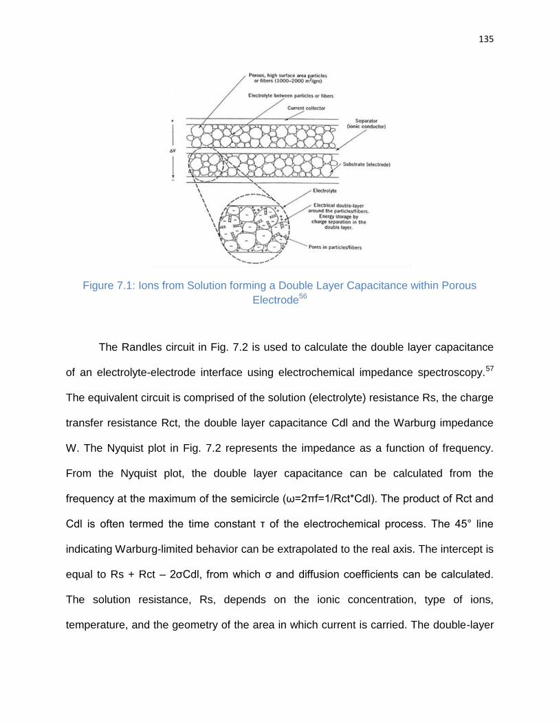
135
Figure 7.1: Ions from Solution forming a Double Layer Capacitance within Porous
Electrode56
The Randles circuit in Fig. 7.2 is used to calculate the double layer capacitance
of an electrolyte-electrode interface using electrochemical impedance spectroscopy.57
The equivalent circuit is comprised of the solution (electrolyte) resistance Rs, the charge
transfer resistance Rct, the double layer capacitance Cdl and the Warburg impedance
W. The Nyquist plot in Fig. 7.2 represents the impedance as a function of frequency.
From the Nyquist plot, the double layer capacitance can be calculated from the
frequency at the maximum of the semicircle (ω=2πf=1/Rct*Cdl). The product of Rct and
Cdl is often termed the time constant τ of the electrochemical process. The 45° line
indicating Warburg-limited behavior can be extrapolated to the real axis. The intercept is
equal to Rs + Rct – 2σCdl, from which σ and diffusion coefficients can be calculated.
The solution resistance, Rs, depends on the ionic concentration, type of ions,
temperature, and the geometry of the area in which current is carried. The double-layer
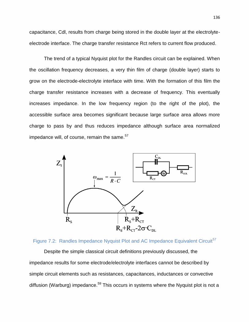
136
capacitance, Cdl, results from charge being stored in the double layer at the electrolyte-
electrode interface. The charge transfer resistance Rct refers to current flow produced.
The trend of a typical Nyquist plot for the Randles circuit can be explained. When
the oscillation frequency decreases, a very thin film of charge (double layer) starts to
grow on the electrode-electrolyte interface with time. With the formation of this film the
charge transfer resistance increases with a decrease of frequency. This eventually
increases impedance. In the low frequency region (to the right of the plot), the
accessible surface area becomes significant because large surface area allows more
charge to pass by and thus reduces impedance although surface area normalized
impedance will, of course, remain the same.57
Figure 7.2: Randles Impedance Nyquist Plot and AC Impedance Equivalent Circuit57
Despite the simple classical circuit definitions previously discussed, the
impedance results for some electrode/electrolyte interfaces cannot be described by
simple circuit elements such as resistances, capacitances, inductances or convective
diffusion (Warburg) impedance.59 This occurs in systems where the Nyquist plot is not a
137
semicircle with the center on the x-axis but instead the observed plot was the arc of a
circle with the center some distance below the x-axis. This trend of semicircle has been
most commonly explained by some property of the system not being homogeneous or
that of the value of some physical property of the system has some frequency
distribution (dispersion). The inhomogeneity or frequency dispersion is generally
attributed to a capacitance dispersion expressed instead in terms of a constant phase
element (CPE). Therefore, constant phase elements (CPE) are used extensively in
equivalent electrical circuits for fitting of experimental impedance data.112-117 The CPE
behavior is induced by varying activation energies on the surface causing
inhomogeneous reaction rates, varying electrode thickness or composition, surface
roughness, fractal geometry, porosity and current and voltage distributions associated
with electrode geometry. For homogenous materials which are acting as ideal
capacitors the impedance is represented by Eq. 1, where i is the imaginary unity and ω
is the cyclic frequency. When there is CPE behavior with inhomogeneity or frequency
dispersion, the impedance is represented by the CPE and defined by two values, CPE-
T and CPE-P described in Eq. 2. CPE-P has a value between –1 and 1 where if CPE-
P=1 then Eq. 2 is identical to that of an ideal capacitor and CPE-T is equal to the
double-layer capacitance (Cdl).
(1) (2)
This study utilizes FeF2 which is a conversion reaction cathode battery material.
Conversion reaction cathodes have been studied as a high energy density replacement
138
option to commercial intercalation secondary batteries for over a decade. However,
commercialization of these electrodes has been obstructed by cycling performance
issues most notably cycling retention and reversibility. Past literature have used FeF2
powder form electrode cycling has been improved through adding conductive matrix
such as carbon to form a nanocomposite. In addition, recently it was shown that canyon
like porous FeF2 thin films of specific optimized porosity percentages have improved
cycling performance. This study uses electrochemical impedance spectroscopy (EIS) as
a method to predict relative comparisons between electrode samples of identical FeF2
composition with the interface double layer capacitance and CPE-T result being
proportional to the accessible surface area hence porosity.
The porous films for this study were produced with a novel thin film deposition
system. The system has the capability to manufacture consistent thin films of a wide
range of thicknesses with unique morphologies which can influence the film’s interfacial
surface area. The system is based on a physical vapor deposition technique called
glancing angle deposition (GLAD) where the morphology of the film growth can be
controlled through substrate rotational positioning at defined oblique angles to the
deposition source.
7.2 Experimental
The thin films were prepared in a custom fabricated high vacuum electron beam
evaporation chamber which has been described elsewhere. The substrate was
prepared using unpolished high-strength aluminum alloy 7075 (McMaster-Carr) with a
thickness of 0.8mm and was cut into a 25mm x 75mm strip. The Al-7075 strip was
139
cleaned with acetone then methanol and placed in substrate holding plate. Two cleaned
glass microscope slides 25mm x 75mm with a thickness of 1mm were placed on each
side of the Al-7075 strip and the three pieces were secured to the substrate holding
plate using Kapton® tape. The glass slides were later used to measure film thickness
with a stylus profilometer.
The source material of approximately 5g total of FeF2 powder (Advanced
Research Chemicals) was packed tightly into three of the four 2cc graphite crucible
liners. The fourth crucible liner was loaded with titanium (99.99% Ti granules, Alfa) as
an adhesion layer. The vacuum chamber was brought to a pressure of 3x10⁻⁶ Torr for
the depositions. The adhesion layer, 50nm of titanium, was first deposited onto the
substrate with an approximate deposition rate of 10A°/sec. Next, FeF2 was deposited
with a rate of approximately 13A°/sec. Once the deposition was completed, the
chamber was vented with a combination of nitrogen then dry air. The films were
removed from chamber, exposed to room atmosphere for approximately 1 minute and
then stored in a helium filled glovebox (<0.6 ppm H2O <0.1 ppm O2) until coin cell
fabrication and characterization trials began. The cell fabrication consisted of punching
14.3mm electrode discs from the film/substrate with a hand press which took place in
room atmosphere for approximately 3 minutes.
7.2.1 Physical Characterization
The thickness of the Ti (50nm adhesion layer) and FeF2 film was analyzed using
the two microscope glass slides substrates with a stylus profilometer (Dektak 150) in
room atmosphere. The alloy Al-7075 substrate had a surface roughness of Ra=0.3
micron so the glass slide allowed for a smoother surface to reference as zero thickness.

140
The FeF2 film with the Ti adhesion layer on the glass substrates were measured in four
locations and an average thickness was calculated and then subtracted by 50nm (the
titanium adhesion layer) to determine the FeF2 film thickness.
X-ray Diffraction (XRD) (Bruker D8 Advance, CuK radiation) was performed in
room atmosphere with a dedicated 10mm x 10mm piece of film.
FeF2 films were analyzed with a Field Emission Scanning Electron Microscopy
(FESEM) (Zeiss) and the films were exposed for approximately 2 minutes to room air
while being mounted in the FESEM.
Image-J, an imaging processing and analysis Java based software (National
Institute of Health, USA) was used to modify the FESEM images into binary images.
These binary images were then used to calculate the canyon facial porosity percentage,
the perimeter length of each canyon and any surface cracks.
7.2.2 Electrochemical Impedance Spectroscopy (EIS)
All batteries fabricated for studies in this paper were aluminized (on the positive
electrode) 2032 coin cells (Hosen) made with cathodes consisting of a 14.3 mm
diameter disc of iron fluoride film, two layers of borosilicate glass fiber separator
(Whatman) with a diameter of 15.9 mm soaked with electrolyte, and a 0.3mm thick
12.7mm diameter lithium metal foil as the anode counter electrode (half-cell) (FMC).
The electrolyte was 1 M LiPF6 EC: DMC purchased from Novolyte, stored in a helium
filled glovebox and used without additional treatment.
Electrochemical impedance spectroscopy (EIS) was performed with a Solartron
Models SI 1287 and SI 1260. The SI 1287 is capable of controlled potential and current
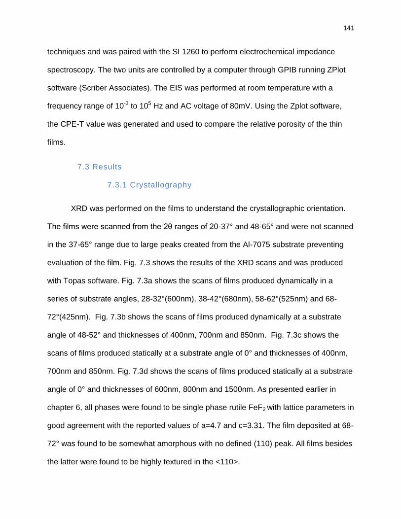
141
techniques and was paired with the SI 1260 to perform electrochemical impedance
spectroscopy. The two units are controlled by a computer through GPIB running ZPlot
software (Scriber Associates). The EIS was performed at room temperature with a
frequency range of 10-3 to 105 Hz and AC voltage of 80mV. Using the Zplot software,
the CPE-T value was generated and used to compare the relative porosity of the thin
films.
7.3 Results
7.3.1 Crystallography
XRD was performed on the films to understand the crystallographic orientation.
The films were scanned from the 2θ ranges of 20-37° and 48-65° and were not scanned
in the 37-65° range due to large peaks created from the Al-7075 substrate preventing
evaluation of the film. Fig. 7.3 shows the results of the XRD scans and was produced
with Topas software. Fig. 7.3a shows the scans of films produced dynamically in a
series of substrate angles, 28-32°(600nm), 38-42°(680nm), 58-62°(525nm) and 68-
72°(425nm). Fig. 7.3b shows the scans of films produced dynamically at a substrate
angle of 48-52° and thicknesses of 400nm, 700nm and 850nm. Fig. 7.3c shows the
scans of films produced statically at a substrate angle of 0° and thicknesses of 400nm,
700nm and 850nm. Fig. 7.3d shows the scans of films produced statically at a substrate
angle of 0° and thicknesses of 600nm, 800nm and 1500nm. As presented earlier in
chapter 6, all phases were found to be single phase rutile FeF2 with lattice parameters in
good agreement with the reported values of a=4.7 and c=3.31. The film deposited at 68-
72° was found to be somewhat amorphous with no defined (110) peak. All films besides
the latter were found to be highly textured in the <110>.
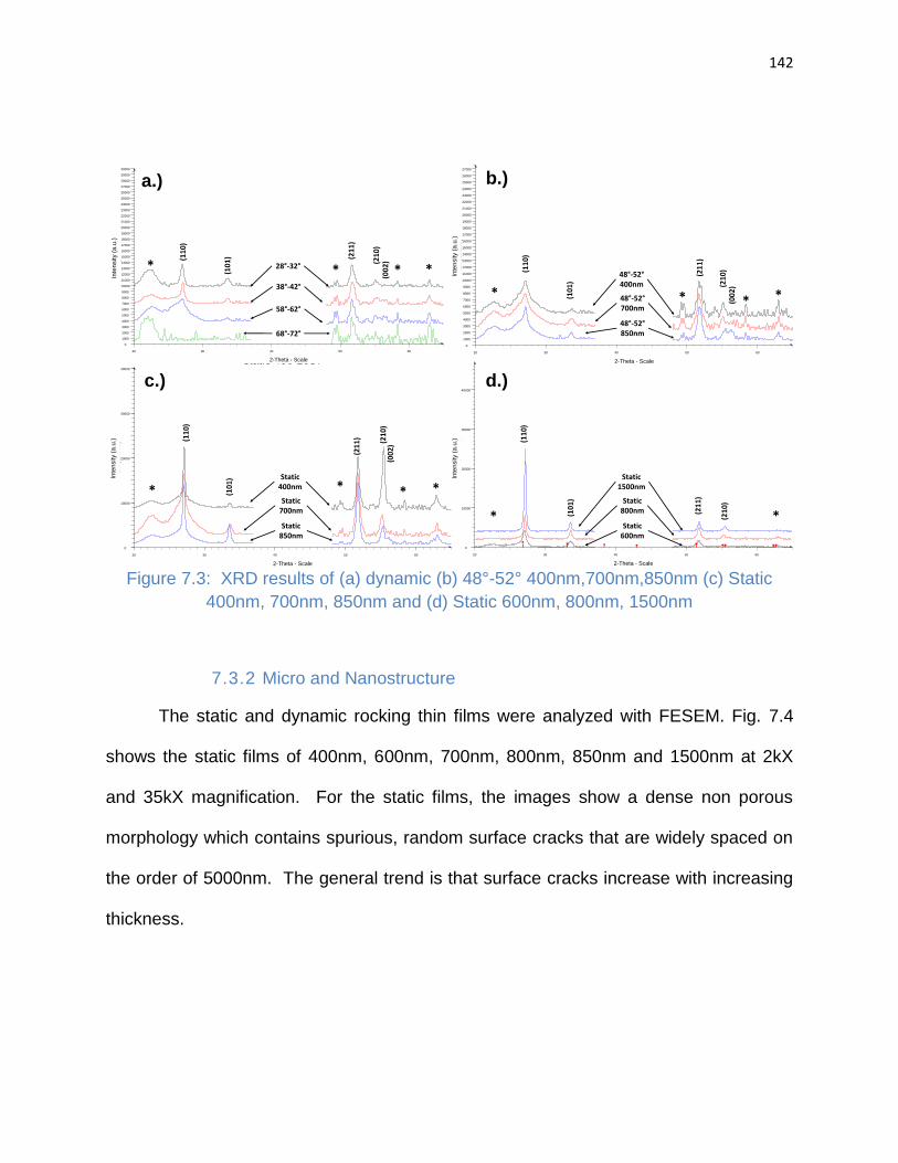
142
Figure 7.3: XRD results of (a) dynamic (b) 48°-52° 400nm,700nm,850nm (c) Static
400nm, 700nm, 850nm and (d) Static 600nm, 800nm, 1500nm
7.3.2 Micro and Nanostructure
The static and dynamic rocking thin films were analyzed with FESEM. Fig. 7.4
shows the static films of 400nm, 600nm, 700nm, 800nm, 850nm and 1500nm at 2kX
and 35kX magnification. For the static films, the images show a dense non porous
morphology which contains spurious, random surface cracks that are widely spaced on
the order of 5000nm. The general trend is that surface cracks increase with increasing
thickness.
3228deg 48-65
Operations: Y Scale Add 1000 | Y Scale Norm 17.671 | Background 0.000,1.000 | Fourier 5.000
7268 4865 - File: 7268_4865.raw - Type: Locked Coupled - Start: 48.000 ° - End: 64.999 ° - Ste
Operations: Y Scale Add 1000 | Y Scale Add -100 | Y Scale Add 100 | Y Scale Norm 5.044 | Ba
7268 2037 - File: 7268_2037.raw - Type: Locked Coupled - Start: 20.000 ° - End: 36.999 ° - Ste
Operations: Y Scale Add -1000 | Y Scale Add 5000 | Y Scale Norm 7.998 | Background 0.000,1.
6258 4865 - File: 6258_4865.raw - Type: Locked Coupled - Start: 48.000 ° - End: 64.999 ° - Ste
Operations: Y Scale Add -1000 | Y Scale Add 5000 | Y Scale Norm 1.367 | Background 0.000,1.
6258 2037 - File: 6258_2037.raw - Type: Locked Coupled - Start: 20.000 ° - End: 36.999 ° - Ste
Operations: Y Scale Add -1000 | Y Scale Add -2000 | Y Scale Add 10000 | Y Scale Norm 5.292
4238_4865 - File: 4238_4865 12-20-12.raw - Type: Locked Coupled - Start: 48.000 ° - End: 64.9
Operations: Y Scale Add 1000 | Y Scale Add -2000 | Y Scale Add -2000 | Y Scale Add 10000 |
4238_2037 - File: 4238_2037 12-20-12.raw - Type: Locked Coupled - Start: 20.000 ° - End: 36.9
Operations: Y Scale Add -2000 | Y Scale Add 12000 | Y Scale Norm 1.765 | Background 0.000,
3228deg 20-37 - File: 3228deg 2037.raw - Type: Locked Coupled - Start: 20.000 ° - End: 36.999
Operations: Y Scale Add -2000 | Y Scale Add 12000 | Y Scale Norm 4.319 | Background 0.000,
3228deg 48-65 - File: 3228_4865.raw - Type: Locked Coupled - Start: 48.000 ° - End: 64.999 ° -
Lin
(C
oun
ts)
0
1000
2000
3000
4000
5000
6000
7000
8000
9000
10000
11000
12000
13000
14000
15000
16000
17000
18000
19000
20000
21000
22000
23000
24000
25000
26000
27000
28000
29000
30000
2-Theta - Scale
20 30 40 50 60
28°-32°
38°-42°
58°-62°
68°-72°
a.)
5248 400 2037
Operations: Y Scale Add 1000 | Y Scale Norm 4.045 | Background 0.000,1.000 | Fourier 5.000 x
5248 850 4865 - File: 5248_850nm_4865.raw - Type: Locked Coupled - Start: 48.000 ° - End: 6
Operations: Y Scale Add 1000 | Background 0.000,1.000 | Fourier 5.000 x 1 | Strip kAlpha2 0.50
5248 850 2037 - File: 5248_850nm_2037.raw - Type: Locked Coupled - Start: 20.000 ° - End: 3
Operations: Y Scale Add 3000 | Y Scale Norm 9.694 | Background 0.000,1.000 | Fourier 5.000 x
5248deg 4865 - File: 5248_700nm_4865.raw - Type: Locked Coupled - Start: 48.000 ° - End: 64
Operations: Y Scale Add 3000 | Y Scale Norm 1.732 | Background 0.000,1.000 | Fourier 5.000 x
5248deg 2037 - File: 5248_700nm_2037.raw - Type: Locked Coupled - Start: 20.000 ° - End: 36
Operations: Y Scale Add 5000 | Y Scale Norm 11.473 | Background 0.000,1.000 | Fourier 5.000
5248 400 4865 - File: 5248_400nm_4865.raw - Type: Locked Coupled - Start: 48.000 ° - End: 6
Operations: Y Scale Add 5000 | Y Scale Norm 2.300 | Background 0.000,1.000 | Fourier 5.000 x
5248 400 2037 - File: 5248_400nm_2037.raw - Type: Locked Coupled - Start: 20.000 ° - End: 3
Lin
(C
ounts
)
0
1000
2000
3000
4000
5000
6000
7000
8000
9000
10000
11000
12000
13000
14000
15000
16000
17000
18000
19000
20000
21000
22000
23000
24000
25000
26000
27000
2-Theta - Scale
20 30 40 50 60
48°-52°400nm
48°-52°700nm
48°-52°850nm
b.)
(11
0)
(21
1)
(10
1) (21
0)
(00
2)
** **
Inte
nsity (
a.u
.)
Inte
nsity (
a.u
.)
(11
0)
(21
1)
(10
1)
(21
0)
(00
2)
** **
static 400 2037
Operations: Y Scale Add 1000 | Y Scale Norm 4.455 | Background 0.000,1.000 | Fourier 5.000 x
static 1000 4865 - File: Static_1000nm_4865.raw - Type: Locked Coupled - Start: 48.000 ° - End
Operations: Y Scale Add 1000 | Y Scale Norm 1.067 | Background 0.000,1.000 | Fourier 5.000 x
static 1000 2037 - File: Static_1000nm_2037.raw - Type: Locked Coupled - Start: 20.000 ° - End
Operations: Y Scale Add 3000 | Y Scale Norm 7.307 | Background 0.000,1.000 | Fourier 5.000 x
static 700 4865 - File: Static_700nm_4865.raw - Type: Locked Coupled - Start: 48.000 ° - End: 6
Operations: Y Scale Add 3000 | Y Scale Norm 1.794 | Background 0.000,1.000 | Fourier 5.000 x
static 700 2037 - File: Static_700nm_2037.raw - Type: Locked Coupled - Start: 20.000 ° - End: 3
Operations: Y Scale Add 2000 | Y Scale Add 2000 | Y Scale Add 5000 | Y Scale Norm 9.255 | B
static 400 4865 - File: Static_400nm_4865.raw - Type: Locked Coupled - Start: 48.000 ° - End: 6
Operations: Y Scale Add 2000 | Y Scale Add 2000 | Y Scale Add 5000 | Background 0.000,1.00
static 400 2037 - File: Static_400nm_2037.raw - Type: Locked Coupled - Start: 20.000 ° - End: 3
Lin
(C
ounts
)
0
10000
20000
30000
40000
2-Theta - Scale
20 30 40 50 60
Static400nm
Static700nm
Static850nm
c.)
Inte
nsity (
a.u
.) (11
0)
(21
1)
(10
1)
(21
0)
(00
2)
** **
Static 1500_2037 3-2-13
00-045-1062 (*) - Iron Fluoride - FeF2 - Y: 3.27 % - d x by: 1. - WL: 1.5406 - Tetragonal - a 4.70
Operations: Y Scale Add -4000 | Y Scale Add 4000 | Background 1.000,1.000 | Fourier 9.873 x
Static 575 4865 3-11-13 - File: Static 575_4865_3-11-13.raw - Type: Locked Coupled - Start: 48.
Operations: Y Scale Add -4000 | Y Scale Add 4000 | Background 1.000,1.000 | Fourier 9.873 x
Static 575 2037 3-11-13 - File: Static 575_2037_3-11-13.raw - Type: Locked Coupled - Start: 20.
Operations: Y Scale Add 2000 | Background 1.000,1.000 | Fourier 9.873 x 1 | Strip kAlpha2 0.50
Static 850 4865 3-7-13 - File: Static 850_4865_3-7-13.raw - Type: Locked Coupled - Start: 48.00
Operations: Y Scale Add 2000 | Background 1.000,1.000 | Fourier 9.873 x 1 | Strip kAlpha2 0.50
Static 850 2037 3-7-13 - File: Static 850_2037_3-7-13.raw - Type: Locked Coupled - Start: 20.00
Operations: Y Scale Add 4000 | Background 1.000,1.000 | Fourier 9.873 x 1 | Strip kAlpha2 0.50
Static 1500_4865 3-2-13 - File: Static 1500_4865_3-2-13.raw - Type: Locked Coupled - Start: 48
Operations: Y Scale Add 4000 | Background 1.000,1.000 | Fourier 9.873 x 1 | Strip kAlpha2 0.50
Static 1500_2037 3-2-13 - File: Static 1500_2037_3-2-13.raw - Type: Locked Coupled - Start: 20
Lin
(C
ounts
)
0
10000
20000
30000
40000
2-Theta - Scale
20 30 40 50 60
Static1500nm
Static800nm
Static600nm
d.)
Inte
nsity (
a.u
.)
(11
0)
(21
1)
(10
1)
(21
0)
* *
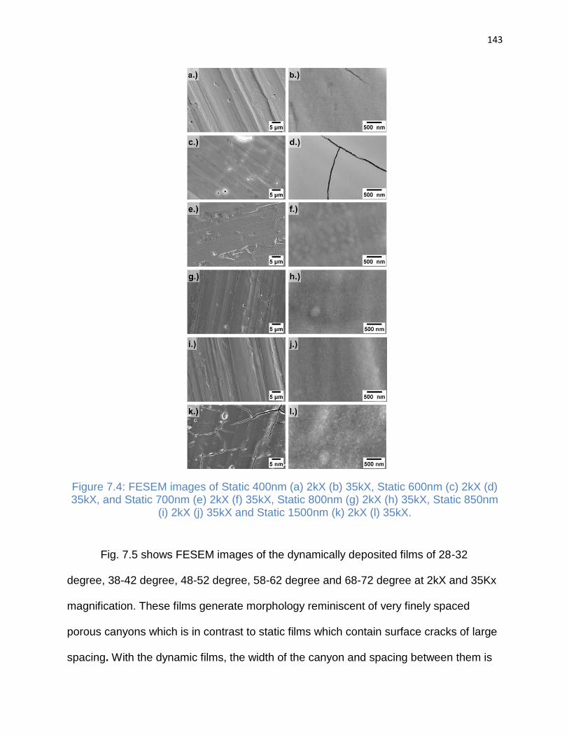
143
Figure 7.4: FESEM images of Static 400nm (a) 2kX (b) 35kX, Static 600nm (c) 2kX (d) 35kX, and Static 700nm (e) 2kX (f) 35kX, Static 800nm (g) 2kX (h) 35kX, Static 850nm
(i) 2kX (j) 35kX and Static 1500nm (k) 2kX (l) 35kX.
Fig. 7.5 shows FESEM images of the dynamically deposited films of 28-32
degree, 38-42 degree, 48-52 degree, 58-62 degree and 68-72 degree at 2kX and 35Kx
magnification. These films generate morphology reminiscent of very finely spaced
porous canyons which is in contrast to static films which contain surface cracks of large
spacing. With the dynamic films, the width of the canyon and spacing between them is
144
dependent on the angle in which the film was deposited. The width and spacing of the
canyons decrease with increasing deposition angle. The film that is deposited at 28-32
degree has the greatest spacing of approximately 1200nm and least amount of porosity
and the 68-72 degree film as the least spacing of approximately 50nm and greatest
porosity. The width of these canyons which appear to be tiger stripe pores when
viewed from above range from approximately 50-150nm depending on the deposition
angle in which the film was deposited.
Figure 7.5: FESEM images of 0.65rpm 28°-32°(a) 2kX (b) 35kX, 38°-42°(c) 2kX (d) 35kX, 48°-52°(e) 2kX (f) 35kX, 58°-62°(g) 2kX (h) 35kX and 68°-72°(i) 2kX (j) 35kX.
7.3.2 Quantitative Microstructure Analysis
Image processing was used to calculate the static and dynamic facial porosity
percentage and the perimeter length of each crack (static) and canyon (dynamic). The

145
FESEM images were modified into binary images using Image-J software which are
shown in Fig. 7.6 and Fig. 7.7. Using the Image-J software, facial porosity area
percentage which is represented in dark contrast and the outlying perimeter length of
the pore were calculated. This pore perimeter length was multiplied by the film
thickness to calculate the additional interfacial surface area created within the canyon
walls.
Figure 7.6: Image processing of 2kX FESEM images of Static 400nm (a), Static 600nm (b), Static 700nm (c), Static 800nm (d), Static 850nm (e) and Static 1500nm (f).
The results in Fig. 7.6 a.), b.), c.), d.), e.), f.) show the images of the 400nm,
600nm, 700nm, 800nm, 850nm and 1500nm respectively. The percentage of facial area
porosity was calculated to be systematically increasing with film thickness; 1.08%
(400nm), 1.68% (600nm), 1.85% (700nm), 1.95% (800nm), 1.29% (850nm) and 3.55%

146
(1500nm). In Fig. 7.10b the total interfacial area including both from facial and perimeter
wall porosity is plotted verse the film thickness. The plot shows a linear dependence
between the facial porosity and thickness. The calculated percentage increase in area
from the perimeter is 5.9% (400nm), 23.7% (600nm), 27.7% (700nm), 15.8% (800nm),
30% (850nm) and 40.4% (1500nm). The dynamic films were deposited with
homogeneous tailored percentages of porosity, in contrast the static films contained non
uniform surface cracking of very low % area. Although, the FESEM and binary images
reveal that the quantity surface cracks and their width generally increase with increasing
thickness, the 800nm and 850nm films are exceptions to this trend. For its thickness,
the 800nm film has relatively fewer cracks which reduces the total pore perimeter length
and causes the percentage increase in area from the perimeter to be reduced.
However, the crack widths of the 800nm film are greater than all of the films except the
1500nm film which causes the facial area porosity to be in agreement with the trend that
facial porosity increases with thickness. For its thickness, the 850nm film has relatively
narrow cracks that are similar in width to a 400nm film which causes the facial area
porosity percentage to be reduced relative to the film’s thickness. However, the 850nm
film has a proportional quantity of cracks for its thickness which causes the total pore
perimeter length to be in agreement with its thickness and hence the percentage
increase in area from the perimeter is in agreement.
The results in Fig. 7.7 a.), b.), c.), d.) and e.) show the images of the 28-32
degree, 38-42 degree, 48-52 degree, 58-62 degree and 68-72 degree respectively. The
simple area percentage of facial porosity and increase in area from the perimeter wall
was calculated to be 5.2%, 103% (28-32 degree), 8.2%, 148% (38-42 degree), 19.9%,
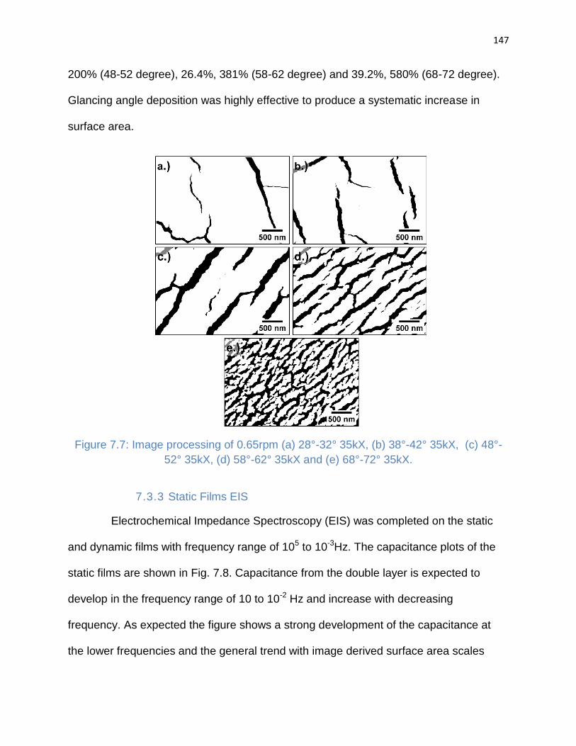
147
200% (48-52 degree), 26.4%, 381% (58-62 degree) and 39.2%, 580% (68-72 degree).
Glancing angle deposition was highly effective to produce a systematic increase in
surface area.
Figure 7.7: Image processing of 0.65rpm (a) 28°-32° 35kX, (b) 38°-42° 35kX, (c) 48°-
52° 35kX, (d) 58°-62° 35kX and (e) 68°-72° 35kX.
7.3.3 Static Films EIS
Electrochemical Impedance Spectroscopy (EIS) was completed on the static
and dynamic films with frequency range of 105 to 10-3Hz. The capacitance plots of the
static films are shown in Fig. 7.8. Capacitance from the double layer is expected to
develop in the frequency range of 10 to 10-2 Hz and increase with decreasing
frequency. As expected the figure shows a strong development of the capacitance at
the lower frequencies and the general trend with image derived surface area scales

148
well. Fig. 7.9 shows the Nyquist plot of the static 400nm film which represents the
general trend of the static films. The Nyquist plots of the static films show a lack of
simple classical circuit behavior and therefore the CPE-T is required to represent the
films. CPE-T was determined by Zplot software and the CPE-T values calculated were
2.82E-05(1500nm), 3.45E-06(850nm), 9.27E-06(800nm), 7.29E-06(700nm), 7.03E-
06(600nm) and 2.61E-06(400nm). CPE-T verse thickness is plotted in Fig.7.10a and
shows how for the static films the CPE-T value increases with increasing thickness.
However, this plot can be slightly misleading because the quantity of surface cracks
increase with increasing thickness, producing more interfacial area. Fig.7.10b shows the
dependence of how the interfacial area increases with increasing thickness. Finally,
Fig.7.10c confirms how CPE-T increases with increasing surface area from cracks
developed by increasing thickness. Therefore, the CPE-T is dependent on the interfacial
surface area from the cracks and not necessarily from the thickness of the film.
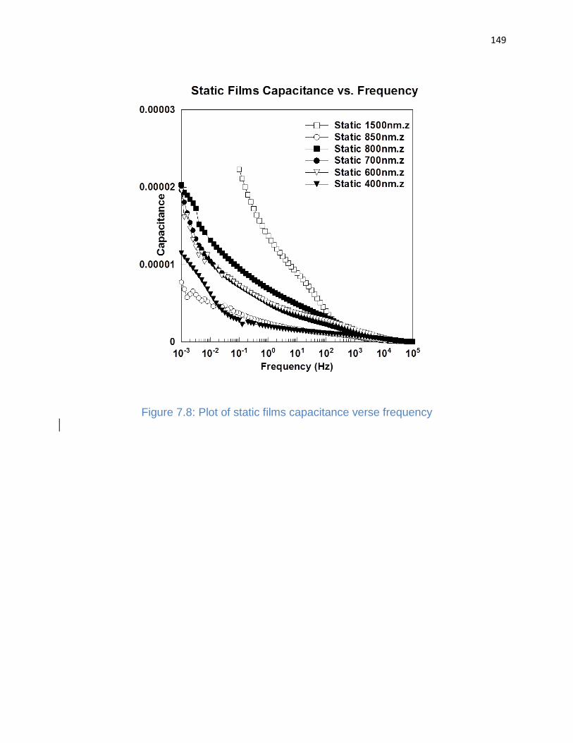
149
Figure 7.8: Plot of static films capacitance verse frequency
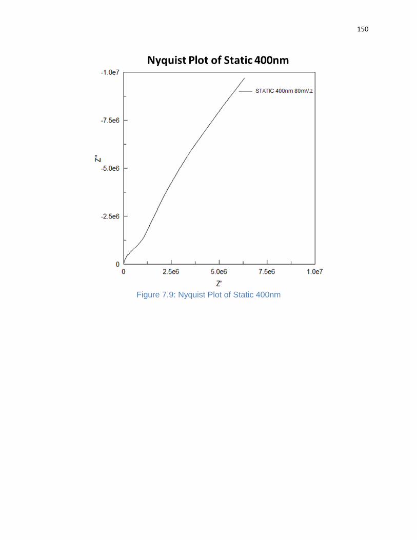
150
Figure 7.9: Nyquist Plot of Static 400nm
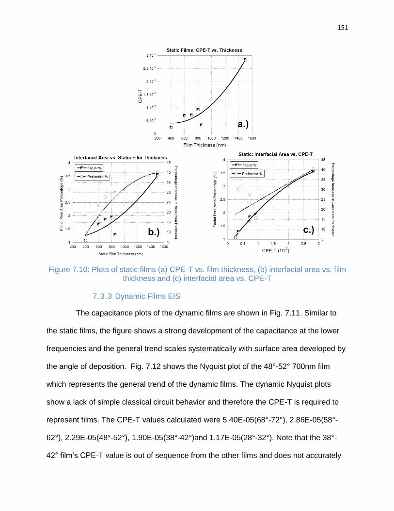
151
Figure 7.10: Plots of static films (a) CPE-T vs. film thickness, (b) interfacial area vs. film thickness and (c) interfacial area vs. CPE-T
7.3.3 Dynamic Films EIS
The capacitance plots of the dynamic films are shown in Fig. 7.11. Similar to
the static films, the figure shows a strong development of the capacitance at the lower
frequencies and the general trend scales systematically with surface area developed by
the angle of deposition. Fig. 7.12 shows the Nyquist plot of the 48°-52° 700nm film
which represents the general trend of the dynamic films. The dynamic Nyquist plots
show a lack of simple classical circuit behavior and therefore the CPE-T is required to
represent films. The CPE-T values calculated were 5.40E-05(68°-72°), 2.86E-05(58°-
62°), 2.29E-05(48°-52°), 1.90E-05(38°-42°)and 1.17E-05(28°-32°). Note that the 38°-
42° film’s CPE-T value is out of sequence from the other films and does not accurately
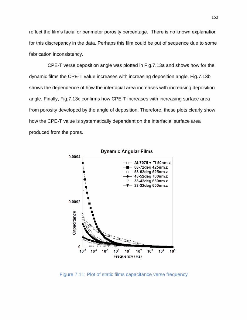
152
reflect the film’s facial or perimeter porosity percentage. There is no known explanation
for this discrepancy in the data. Perhaps this film could be out of sequence due to some
fabrication inconsistency.
CPE-T verse deposition angle was plotted in Fig.7.13a and shows how for the
dynamic films the CPE-T value increases with increasing deposition angle. Fig.7.13b
shows the dependence of how the interfacial area increases with increasing deposition
angle. Finally, Fig.7.13c confirms how CPE-T increases with increasing surface area
from porosity developed by the angle of deposition. Therefore, these plots clearly show
how the CPE-T value is systematically dependent on the interfacial surface area
produced from the pores.
Figure 7.11: Plot of static films capacitance verse frequency
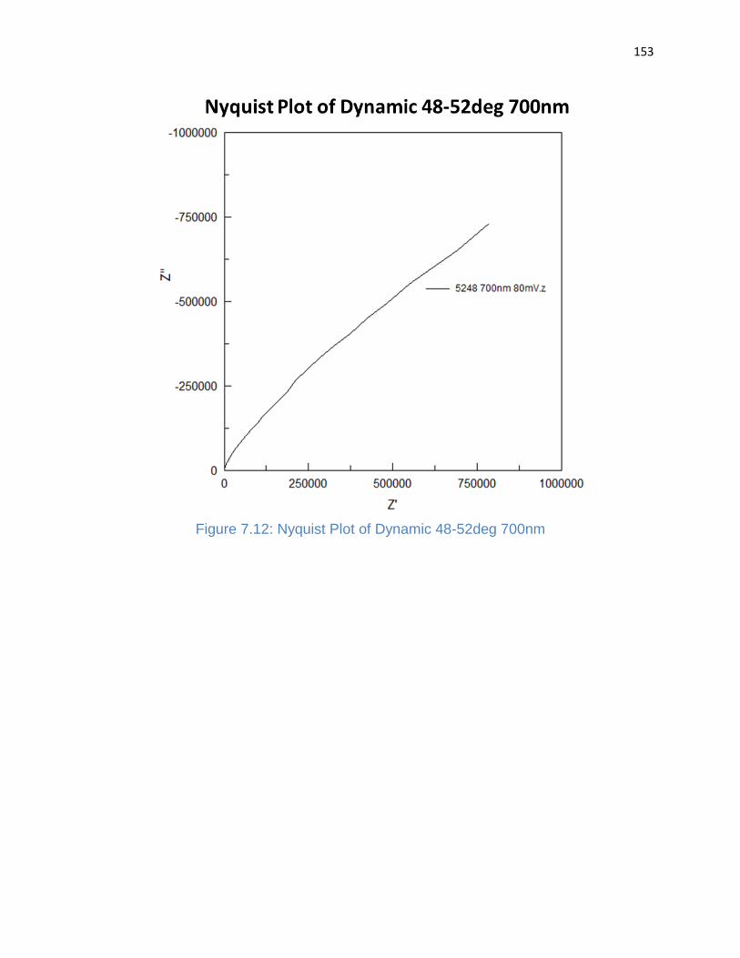
153
Figure 7.12: Nyquist Plot of Dynamic 48-52deg 700nm
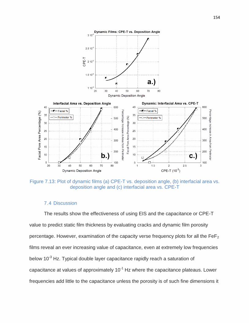
154
Figure 7.13: Plot of dynamic films (a) CPE-T vs. deposition angle, (b) interfacial area vs. deposition angle and (c) interfacial area vs. CPE-T
7.4 Discussion
The results show the effectiveness of using EIS and the capacitance or CPE-T
value to predict static film thickness by evaluating cracks and dynamic film porosity
percentage. However, examination of the capacity verse frequency plots for all the FeF2
films reveal an ever increasing value of capacitance, even at extremely low frequencies
below 10-3 Hz. Typical double layer capacitance rapidly reach a saturation of
capacitance at values of approximately 10-1 Hz where the capacitance plateaus. Lower
frequencies add little to the capacitance unless the porosity is of such fine dimensions it
155
requires the stripping of the salvation sphere around the ion of interest for the ion to
enter the site. The increasing capacitance without an eventual plateau could be from a
redox which might be occurring on the surface of the electrode. The studies were
performed at an open circuit voltage of approximately 3V, which is well above the
conversion potential of FeF2 2 LiF + Fe of approximately 2.6V. The AC sweep was
limited to a very small value of 80mV that still keeps the minimum voltage value well
above that of the conversion reaction. Possibilities to explain this behavior can be
related to a surface and subsurface phase containing Fe3+ species. In this case, the
reduction would occur in the 3V range. Also, there may be very fine porosity that is not
readily apparent from micrographs that induce the aforementioned solvent stripping.
The sample size was by far too small to allow the characterization by BET, but small
angle x-ray diffraction (SAXS) and other techniques would be of use to explore to define
with more precision.
7.5 Conclusion
Typically, establishing true surface area of a thin film is very tedious done
through BET, this study has shown that EIS can routinely establish absolute surface
area or a relative difference in surface area from a known standard. In addition, is has
been shown that EIS can predict static film thickness simply based on development of a
small percentage of stress cracks. The method of using EIS to predict interfacial surface
area is highly beneficial. The method is faster, more cost effective, and more accurate
(electrolyte accessible service will only be measured) than BET or using electron
microscopy along with an imaging software. This study has shown the effectiveness of
GLAD to develop films of high texture and porosity. Using the GLAD fabrication method

156
films with tailored percentages of increasing porosity were produced which allowed for
the EIS capacitance and CPE-T to be correlated systematically.
157
8 Future Work
This research of applying 3D nanostructured porous electrodes to conversion
reaction type batteries is only the initial work. The fact that these electrodes are 6x
thicker than previous electrochemical studies with FeF2 films yet have improved
performance, has provided insight into constructing metal fluoride conversion electrodes
which are limited by their wide band gap. This research has provided a new insight in
improving the performance of conversion materials for researchers to consider and has
opened the door for future studies using different design and fabrication techniques for
producing 3D structures. Among these techniques but not limited to are template
synthesis as a means of producing nanotubes, nanowires, and nanorods, other GLAD
methods discussed earlier and laser etching. In addition, would be interesting to apply
the GLAD fabrication method used in this study and new techniques to other conversion
reaction electrode materials to better understand their reaction mechanisms and
improve cycling performance. In addition, more refinement is needed in predicting
porosity content in conversion electrodes by Electrochemical Impedance Spectroscopy
(EIS). This will allow for a highly reliable, quick and inexpensive method to determine
the porosity of conversion electrodes in the future. Metal fluorides such as FeF2, have
the potential to be relatively less expensive battery materials with high capacity. It is
important to continue to increase the thickness of these electrodes, such as this study
has done in order to gain greater potential energy storage and allow conversion
electrodes to be more viable.
158
9 Summary
• A custom e-beam chamber was designed and fabricated to apply novel dynamic
rotation of the substrate which can tailor the percentage of porosity in thin films.
• E-beam Deposition and aluminum substrates were used for the first time to
produce metal fluoride electrodes (FeF2) for batteries.
• The dynamic films in this study significantly improve electrochemical
performance over statically produced dense films.
• The dynamic porous films were six times in magnitude thicker than previous
electrochemical studies with FeF2 films yet have improved performance.
• This study showed that the performance of conversion reaction electrodes can
be improved with deep channeled porosity.
• Electrochemical Impedance Spectroscopy (EIS) can routinely establish absolute
surface area or a relative difference in surface area from a known standard
allowing for an alternative means to predict the percentage of porosity.
159
10 References
1 M. S. Whittingham , Proceedings of the IEEE , May (2012), Vol. 100.
2 R.E. Doe, K. A. Persson, Y. S. Meng, and G. Ceder, Chem. Mater. (2008), 20, 5274–5283.
3 B. Dunn, H. Kamath, J.M. Tarascon, Science, (2011), 334, 928.
4 G.G. Amatucci, N. Pereira, Journal of Fluorine Chemistry 128 (2007) 243–262.
5 A.J. Gmitter, PhD Dissertation, Rutgers, the State University of New Jersey (2012).
6 Y. Ma and S. Garofalini, J. Am. Chem. Soc. (2012), 134, 8205−8211.
7 F. Wang, R. Robert, N. Chernova, N. Pereira, F. Omenya, F. Badway, X. Hua, M. Ruotolo, R.
Zhang, L. Wu, V. Volkov, D. Su, B. Key, M. S. Whittingham, C. P. Grey, G.G. Amatucci, Y. Zhu, J.
Graetz, J. Am. Chem. Soc. (2011), 133, 18828–18836.
8 Yang Zhen-hua, Wang Xian-you, Liu Li, Su Xu-ping, Trans. Nonferrous Met. Soc. China 22(2012)
286−390.
9 Reinaldo Santos-Ortiz, Vyacheslav Volkov, Stefan Schmid, Fang-Ling Kuo, Kim
Kisslinger, Soumya Nag, Rajarshi Banerjee, Yimei Zhu, and Nigel D Shepherd, ACS Appl. Mater.
Interfaces, (2013).
10 Badway, F., Pereira, N., Cosandey, F., & Amatucci, G. G., Journal of The Electrochemical
Society, (2003),150(9), A1209-A1218.
11 Liao P., MacDonald B., Dunlap R.A., & Dahn J.R, Chem. Mater., (2008), 20, 454–461.
12 Wang, F., Robert, R., Chernova, N. A., Pereira, N., Omenya, F., Badway, F. & Graetz, J., Journal
of the American Chemical Society, (2011), 133(46), 18828-18836.
13 J.B. Bates, N.J. Dudney, B. Neudecker, A. Ueda, C.D. Evan, Solid State Ionics 135 (2000) 33 –
45.
14 N.J. Dudney, B.J. Neudecker, Curr. Opin. Solid State Mater. Sci. 4 (1999) 479–482.
15 N. J. Dudney, Y. Jang, Journal of Power Sources 119–121 (2003) 300–304.
16 X. Yu, J.B. Bates, G.E. Jellison, F.X. Hart, J. Electrochem. Soc. 144 (1997) 524.
17 Cairns, E. J.; Shimotake, H. Science (1969), 164, 1347.
18 Kennedy J. and Hunter, J., J. Electrochem. Soc. (1976), Volume 123, Issue 1, Pages 10-14.
19 F. Badway, A.N. Mansour, N. Pereira, J.F. Al-Sharab, F. Cosandey, I. Plitz, G.G. Amatucci,
Chem. Mater. 19 (2007) 4129.
20 Yan-Hua Cui, Ming-Zhe Xue, Yong-Ning Zhou, Shu-Ming Peng, Xiao-Lin Wang, Zheng-Wen Fu,
Electrochimica Acta 56 (2011) 2328–2335.
21 Zheng-Wen Fu, Chi-Lin Li, Wen-Yuan Liu, Jun Ma, Ying Wang and Qi-Zong Qin, J. Electrochem.
Soc. 2005, Volume 152, Issue 2, Pages E50-E55.
22 Makimura, Y., Rougier, A., Tarascon, J.M., Applied Surface Science 252 (2006) 4587–4592.
23 P. Fiordiponti, S. Panero, G. Pistoia, C. Temperoni, J. Electrochem. Soc. 125 (1978) 511–515.
24 Gmitter, A.J., Halajko, A., Sideris, P.J., Greenbaumb, S.G., Amatucci, G.G., Electrochimica Acta
88 (2013) 735– 744.

160
25 Hua Zhang, Yong-Ning Zhou, Qian Sun, Zheng-Wen Fu, Solid State Sciences 10 (2008) 1166-
1172.
26 F. Badway, N. Pereira, F. Cosandey, G.G. Amatucci, J. Electrochem. Soc. 150 (2003) A1318.
27 Cui Yan-Hua, Xue Ming-Zhe, Hu Ke, Li Da, Wang Xiao-Lin, Su Wei, Liu Xiao-Jiang, Meng Fan-
Ming, Zheng-Wen Fu, Journal of Organic Materials, (2010), Vol 25(2).
28 S V Kuznetsov, V V Osiko, E A Tkatchenko, P P Fedorov, Russian Chemical Reviews, (2006), 75
(12) 1065 – 1082.
29 Domange, L., Ann. chinz.,(1937) 7, 225.
30 Nogues, J., Lederman, D., Moran, T.J., Schuller, I.K., Physical Review Letters, (1996), Volume
76, Number 24.
31 Yamazaki, H., Satooka, J. , RIKEN Review, Focused on Nanotechnology Review (Aug 2001), No.
38.
32 Nishizawa, M., Mukai, K., Kuwabata, S., Martin, C. R., & Yoneyama, H. (1997). Journal of the
Electrochemical Society, 144(6), 1923-1927.
33 Li, N., Patrissi, C. J., Che, G., & Martin, C. R. (2000). Journal of the electrochemical Society,
147(6), 2044-2049.
34 Li, N., Martin, C. R., & Scrosati, B. (2000). Electrochemical and solid-state letters, 3(7), 316-318.
35 Fan, J., Wang, T., Yu, C., Tu, B., Jiang, Z., & Zhao, D. (2004). Advanced Materials, 16(16), 1432-
1436.
36 Chan, C. K., Peng, H., Liu, G., McIlwrath, K., Zhang, X. F., Huggins, R. A., & Cui, Y. (2007).
Nature nanotechnology, 3(1), 31-35.
37 Jiao, F., Bao, J., Hill, A. H., & Bruce, P. G. (2008). Angewandte Chemie, 120(50), 9857-9862.
38 Wang, Y., & Cao, G. (2008). Advanced Materials,20(12), 2251-2269.
39 Oh, S. W., Myung, S. T., Bang, H. J., Yoon, C. S., Amine, K., & Sun, Y. K. (2009).
Electrochemical and Solid-State Letters, 12(9), A181-A185.
40 Zhang, Y., Liu, Y., & Liu, M. (2006). Chemistry of materials, 18(19), 4643-4646.
41 Fleischauer, M. D., Li, J., & Brett, M. J. (2009). Journal of The Electrochemical Society, 156(1),
A33-A36.
42 Pröll, J., Kohler, R., Adelhelm, C., Bruns, M., Torge, M., Heißler, S., Pfleging, W. (2011,
February). In Proc. SPIE (Vol. 7921, p. 79210Q).
43 Bettge, M., Ryu, S. Y., MacLaren, S., Burdin, S., Petrov, I., Yu, M. F., Abraham, D. P. (2012).
Journal of Power Sources.
44 Arthur, T. S., Bates, D. J., Cirigliano, N., Johnson, D. C., Malati, P., Mosby, J. M., Dunn, B.
(2011). MRS bulletin, 36(07), 523-531.
45 O. Barbieri, M. Hahn, A. Herzog, and R. Kötz, Carbon, 43, 1303 (2005).
46 M. Endo, T. Maeda, T. Takeda, et al., J. Electrochem. Soc., 148, A910 (2001).
47 G. Salitra, A. Soffer, L. Eliad, Y. Cohen, D. Aurback, J. Electrochem. Soc., 147, 2486 (2000).

161
48 H. Tamai, M. Kouzu, M. Morita, H. Yasuda, Electrochem. Solid-State Lett. 6 (2003) A214.
49 Y. Yamada, O. Tanaike, T. T. Liang, H. Hatori, S. Shiraishi, A. Oya, Electrochem. Solid-State
Lett. (2002) A283.
50 S. Yoon, J. Lee, T. Hyeon, S.M. Oh, J. Electrochem. Soc. 147 (2000) 2507.
51 Yu, Y., Gu, L., Dhanabalan, A., Chen, C. H., & Wang, C. (2009). Electrochimica Acta, 54(28),
7227-7230.
52 Leng, Y., Chan, S. H., & Liu, Q. (2008). International Journal of Hydrogen Energy, 33(14), 3808-
3817.
53 Da Silva, L. M., Fernandes, K. C., De Faria, L. A., & Boodts, J. F. (2004). Electrochimica acta,
49(27), 4893-4906.
54 Opitz, A. K., & Fleig, J. (2010). Solid State Ionics, 181(15), 684-693.
55 Robyr, C., Agarwal, P., Mettraux, P., & Landolt, D. (1997). Thin solid films, 310(1), 87-93.
56 P. Simon, A. Burke, the Electrochemical Society Interface, Spring 2008.
57 F. Lisdat, D. Schäfer Anal Bioanal Chem (2008) 391:1555–1567.
58 C.Gabrielli, Solartron Analytical, Technical Report (1998) 004/83, Issue 3.
59 J. B. Jorcin, M. E. Orazem, N. Pébère, B. Tribollet, Electrochimica Acta 51 (2006) 1473–1479.
60 J. N. Barisci, G. G. Wallace, D. Chattopadhyay, F. Papadimitrakopoulos, R. H. Baughmanc,
Journal of The Electrochemical Society, (2003), 150, E409-E415.
61 MIT OpenCourseWare, Electrochemical Energy Systems, Spring 2011.
62 D. Qu, Journal of Power Sources (2001), 102, 270–276.
63 J. M. Lafferty, Foundations of vacuum science and technology, New York: Wiley, 1998.
64 D. Mattox, Handbook of physical vapor deposition (PVD) processing, Elsevier Inc., 2010.
65 D. L. Smith, Thin-film deposition: principles and practice, New York: McGraw-Hill, 1995.
66 Brooks Automation CTI-Cryogenics Owner’s Manual.
67 Vacuum Technology,(2002), 60A & 60B p171-212.
68 E.Chen, Applied Physics 298r Lecture Notes, (4-12-2004).
69 http://groups.ist.utl.pt/rschwarz/rschwarzgroup_files/PLD_files/PLD.htm.
70 http://www.iestechsales.com.
71 www.wfu.edu/~ucerkb/Nan242/L11-Thin_Film_Growth.pdf.
72 Glancing Angle Deposition Research Group, University of Alberta,
http://www.ece.ualberta.ca/~glad/glad.html
73 Y.-P. Zhao, D.-X. Ye, G.-C. Wang and T.-M. Lu, Proceedings of SPIE, (2003), Vol. 5219
Nanotubes and Nanowires pages 59-73.
74 B. Dick, M. J. Brett, T. Smy, J. Vac. Sci. Technol., (Nov/Dec 2003) B 21, 6.
75 Ormec Servo Motion Controller User Manual, 1995.
76 http://prism.mit.edu/xray/Basics%20of%20X-Ray%20Powder%20Diffraction.pdf.
77 http://www.lesker.com.
162
78 Rougier, Y. Makirnura, N. Penin, X. Darok and J.-M. Tarascon, M. J. Condensed Mater, (January
2006), Volume7, number 1.
79 M. R. Fitzsimmons, C. Leighton, J. Nogue´s, A. Hoffmann, Kai Liu, C. F. Majkrzak, J. A. Dura, J.
R. Groves, R. W. Springer, P. N. Arendt, V. Leiner, H. Lauter, Ivan K. Schuller, Physical Review
B, Volume 65, 134436.
80 M. Birkholz, J. Appl. Cryst. (2007). 40, 735–742.
81 H-R Wenk1 and P Van Houtte, Rep. Prog. Phys., (2004), 67, 1367–1428.
82 J. Nogue´s, T. J. Moran, D. Lederman, I. K. Schuller, K. V. Rao, Physical Review B, (March
1999),Volume 59, Number 10.
83 Poizot, P., Laruelle, S., Grugeon, S., Dupont, L., & Tarascon, J. M. (2000). Nano-sized transition-
metal oxides as negative-electrode materials for lithium-ion batteries. Nature, 407(6803), 496-
499.
84 Grugeon, S., Laruelle, S., Herrera-Urbina, R., Dupont, L., Poizot, P., & Tarascon, J. M. (2001).
Particle size effects on the electrochemical performance of copper oxides toward lithium. Journal
of The Electrochemical Society, 148(4), A285-A292.
85 Bervas, M., Badway, F., Klein, L. C., & Amatucci, G. G. (2005). Bismuth fluoride nanocomposite
as a positive electrode material for rechargeable lithium batteries. Electrochemical and Solid-
State Letters, 8(4), A179-A183.
86 Tarascon, J. M., Grugeon, S., Morcrette, M., Laruelle, S., Rozier, P., & Poizot, P. (2005). New
concepts for the search of better electrode materials for rechargeable lithium batteries. Comptes
Rendus Chimie, 8(1), 9-15.
87 Amatucci, G. G., & Pereira, N. (2007). Fluoride based electrode materials for advanced energy
storage devices. Journal of Fluorine Chemistry, 128(4), 243-262.
88 Débart, A., Dupont, L., Patrice, R., & Tarascon, J. M. (2006). Reactivity of transition metal (Co, Ni,
Cu) sulphides versus lithium: The intriguing case of the copper sulphide. Solid state sciences,
8(6), 640-651.
89 Ji, X., & Nazar, L. F. (2010). Advances in Li–S batteries. J. Mater. Chem., 20(44), 9821-9826.
90 Pralong, V., Leriche, J. B., Beaudoin, B., Naudin, E., Morcrette, M., & Tarascon, J. M. (2004).
Electrochemical study of nanometer Co< sub> 3</sub> O< sub> 4</sub>, Co, CoSb< sub>
3</sub> and Sb thin films toward lithium. Solid State Ionics, 166(3), 295-305.
91 Taberna, P. L., Mitra, S., Poizot, P., Simon, P., & Tarascon, J. M. (2006). High rate capabilities
Fe3O4-based Cu nano-architectured electrodes for lithium-ion battery applications. Nature
materials, 5(7), 567-573.
92 Balaya, P., Li, H., Kienle, L. & Maier, J. (2003). Fully reversible homogeneous and heterogeneous
Li-storage in RuO2 with high capacity. Adv. Funct. Mater. 13, 621–625.
93 Badway, F., Cosandey, F., Pereira, N., & Amatucci, G. G. (2003). Carbon metal fluoride
nanocomposites high-capacity reversible metal fluoride conversion materials as rechargeable

163
positive electrodes for Li batteries. Journal of The Electrochemical Society, 150(10), A1318-
A1327.
94 Nishijima, M., Gocheva, I. D., Okada, S., Doi, T., Yamaki, J. I., & Nishida, T. (2009). Cathode
properties of metal trifluorides in Li and Na secondary batteries. Journal of Power Sources,
190(2), 558-562.
95 Pereira, N., Klein, L. C., & Amatucci, G. G. (2002). The Electrochemistry of Zn3 N 2 and LiZnN A
Lithium Reaction Mechanism for Metal Nitride Electrodes. Journal of The Electrochemical
Society, 149(3), A262-A271.
96 Pereira, N., Balasubramanian, M., Dupont, L., McBreen, J., Klein, L. C., & Amatucci, G. G.
(2003). The electrochemistry of germanium nitride with lithium. Journal of The Electrochemical
Society, 150(8), A1118-A1128.
97 Pralong, V., Souza, D. C. S., Leung, K. T., & Nazar, L. F. (2002). Reversible lithium uptake by
CoP< sub> 3</sub> at low potential: role of the anion. Electrochemistry communications, 4(6),
516-520.
98 Silva, D. C. C., Crosnier, O., Ouvrard, G., Greedan, J., Safa-Sefat, A., & Nazar, L. F. (2003).
Reversible lithium uptake by FeP2. Electrochemical and solid-state letters, 6(8), A162-A165.
99 Badway, F., Pereira, N., Cosandey, F., & Amatucci, G. G. (2003). Carbon-Metal Fluoride
Nanocomposites Structure and Electrochemistry of. Journal of The Electrochemical Society,
150(9), A1209-A1218.
100 Wang, F., Robert, R., Chernova, N. A., Pereira, N., Omenya, F., Badway, F., ... & Graetz, J.
(2011). Conversion Reaction Mechanisms in Lithium Ion Batteries: Study of the Binary Metal
Fluoride Electrodes. Journal of the American Chemical Society, 133(46), 18828-18836.
101 Ko, J. K. (n.d.). FeF2 conductivity measurement study. Rutgers University.
102 Robbie, K., & Brett, M. J. (1997). Sculptured thin films and glancing angle deposition: Growth
mechanics and applications. Journal of Vacuum Science & Technology A: Vacuum, Surfaces,
and Films, 15(3), 1460-1465.
103 Robbie, K., Sit, J. C., & Brett, M. J. (1998). Advanced techniques for glancing angle deposition.
Journal of Vacuum Science & Technology B: Microelectronics and Nanometer Structures, 16(3),
1115-1122.
104 Makimura, Y., Rougier, A., & Tarascon, J. M. (2006). Pulsed laser deposited iron fluoride thin
films for lithium-ion batteries. Applied surface science, 252(13), 4587-4592.
105 Ma, Y., & Garofalini, S. H. (2012). Atomistic Insights into the Conversion Reaction in Iron
Fluoride: A Dynamically Adaptive Force Field Approach. Journal of the American Chemical
Society, 134(19), 8205-8211.
106 Liao P., MacDonald B., Dunlap R.A., & Dahn J.R (2008). Combinatorially Prepared [LiF]1-xFex
Nanocomposites for Positive Electrode Materials in Li-Ion Batteries. Chem. Mater., 20, 454–461.
164
107 Wang, F., Yu, H. C., Chen, M. H., Wu, L., Pereira, N., Thornton, K., Graetz, J. (2012). Tracking
lithium transport and electrochemical reactions in nanoparticles. Nature Communications, 3,
1201.
108 Li, N., Martin, C. R., & Scrosati, B. (2000). A High‐Rate, High‐Capacity, Nanostructured Tin Oxide
Electrode. Electrochemical and solid-state letters, 3(7), 316-318.
109 Wu, M. S., Chiang, P. C. J., Lee, J. T., & Lin, J. C. (2005). Synthesis of manganese oxide
electrodes with interconnected nanowire structure as an anode material for rechargeable lithium
ion batteries. The Journal of Physical Chemistry B, 109(49), 23279-23284.
110 A.J. Gmitter, F. Badway, S. Rangan, R.A. Bartynski, A. Halajko, N. Pereira, G.G. Amatucci,
(2010), Formation, dynamics, and implication of solid electrolyte interphase in high voltage
reversible conversion fluoride nanocomposites, Journal of Materials Chemistry 20, 4149.
111 Gmitter, A. J., Halajko, A., Sideris, P. J., Greenbaum, S. G., & Amatucci, G. G. (2012).
Subsurface diffusion of oxide electrolyte decomposition products in metal fluoride nanocomposite
electrodes. Electrochimica Acta.
112 Qian, X., Gu, N., Cheng, Z., Yang, X., Wang, E., & Dong, S. (2001). Impedance study of (PEO)<
sub> 10</sub> LiClO< sub> 4</sub>–Al< sub> 2</sub> O< sub> 3</sub> composite polymer
electrolyte with blocking electrodes. Electrochimica acta, 46(12), 1829-1836.
113 Fekry, A. M., Gasser, A. A., & Ameer, M. A. (2010). Corrosion protection of mild steel by
polyvinylsilsesquioxanes coatings in 3% NaCl solution. Journal of applied electrochemistry, 40(4),
739-747.
114 Jarjoura, G., & Kipouros, G. J. (2006). Effect of nickel on copper anode passivation in a copper
sulfate solution by electrochemical impedance spectroscopy. Journal of applied electrochemistry,
36(6), 691-701.
115 Eldarrat, A. H., Wood, D. J., Kale, G. M., & High, A. S. (2007). Age-related changes in ac-
impedance spectroscopy studies of normal human dentine. Journal of Materials Science:
Materials in Medicine, 18(6), 1203-1210.
116 Proskuryakov, Y. Y., Durose, K., Taele, B. M., & Oelting, S. (2007). Impedance spectroscopy of
unetched CdTe/CdS solar cells—equivalent circuit analysis. Journal of Applied Physics, 102(2),
024504-024504.
117 Macdonald, J. R. (1987). Impedance spectroscopy and its use in analyzing the steady-state AC
response of solid and liquid electrolytes. Journal of electroanalytical chemistry and interfacial
electrochemistry, 223(1), 25-50.
165
11 Curriculum vitae
EDUCATION____________________________________________________________________ Doctor of Philosophy Rutgers, the State University of New Jersey Material Science and Engineering May 2013 New Brunswick, NJ Master of Engineering in Automotive Engineering University of Michigan
Ann Arbor, MI Bachelor of Science in Mechanical Engineering Michigan Technological University Houghton, MI
INDUSTRY EXPERIENCE_________________________________________________________ Design Engineer Toyota Technical Center, Ann Arbor, MI
Design Engineer Honda Research and Development, Raymond, OH
Product Engineer Chrysler Technical Center, Auburn Hills, MI
COMMERCIALIZED INDUSTRY PATENTS_________________________________________________
1.) US Patent 8,308,226: Parkinson Matthew Frank, Steinbrecher Robert Charles; November 13, 2012; Toyota Motor Engineering & Manufacturing North America, Inc.
2.) US Patent 8,196,987: Parkinson Matthew Frank, Steinbrecher Robert Charles; June 12, 2012; Toyota Motor Engineering & Manufacturing North America, Inc.
3.) US Patent 8,167,347: Parkinson Matthew Frank, Steinbrecher; Robert Charles; May 1, 2012; Toyota Motor Engineering & Manufacturing North America, Inc.
4.) US Patent 8,011,714: Parkinson Matthew Frank, Steinbrecher Robert Charles, Dhamrat Hamshivraj Singh, Deming; William; September 6, 2011; Toyota Motor Engineering & Manufacturing North America, Inc.
5.) US Patent 7,823,947: Parkinson Matthew Frank, Steinbrecher Robert Charles; November 2, 2010; Toyota Motor Engineering & Manufacturing North America, Inc.
6.) US Patent 11,609,479: Matt Parkinson, Yukio Akimoto, John Hwang; June 21, 2007; Honda Motor Co. Ltd.
PUBLICATIONS AND PRESENTATIONS__________________________________________________
Parkinson M., Ko J., Halajko A., Sanghvia S. and Amatucci G.G. Effect of Vertically Structured Porosity on Electrochemical Performance of FeF2 Films for Lithium Batteries. Journal of Materials Chemistry A. (Submitted March 2013).
Parkinson M., Vaning B., Gural J., and Amatucci G.G. Design of a Servo Controlled Rotating Substrate Drum Containing Deposition Height Adjustment. 54th Annual Society of Vacuum Coaters Technical Conference, Chicago, IL April 16–21, 2011.