Embed Size (px)
DESCRIPTION
gates ppt
Citation preview

HistoryHistory
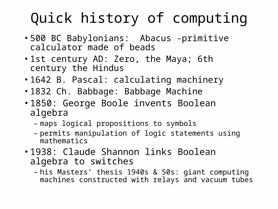
Quick history of computing• 500 BC Babylonians: Abacus -primitive calculator
made of beads• 1st century AD: Zero, the Maya; 6th century the
Hindus • 1642 B. Pascal: calculating machinery• 1832 Ch. Babbage: Babbage Machine• 1850: George Boole invents Boolean algebra
– maps logical propositions to symbols– permits manipulation of logic statements using mathematics
• 1938: Claude Shannon links Boolean algebra to switches– his Masters’ thesis 1940s & 50s: giant computing machines
constructed with relays and vacuum tubes
3
A quick history lesson
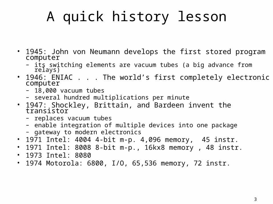
• 1945: John von Neumann develops the first stored program computer– its switching elements are vacuum tubes (a big advance from relays)
• 1946: ENIAC . . . The world’s first completely electronic computer– 18,000 vacuum tubes– several hundred multiplications per minute
• 1947: Shockley, Brittain, and Bardeen invent the transistor– replaces vacuum tubes– enable integration of multiple devices into one package– gateway to modern electronics
• 1971 Intel: 4004 4-bit m-p. 4,096 memory, 45 instr.• 1971 Intel: 8008 8-bit m-p., 16kx8 memory , 48 instr.• 1973 Intel: 8080 • 1974 Motorola: 6800, I/O, 65,536 memory, 72 instr.
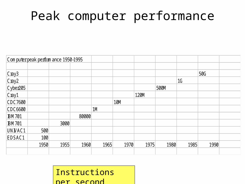
Computer peak performance 1950-1995
Cray3 50GCray2 1GCyber205 500MCray1 120MCDC7600 10MCDC6600 1MIBM701 80000IBM701 3000UNIVAC1 500EDSAC1 100
1950 1955 1960 1965 1970 1975 1980 1985 1990
Peak computer performance
Instructions per second
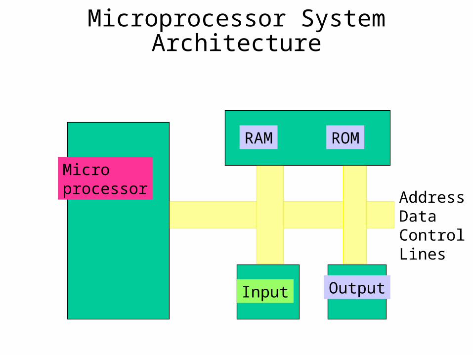
Microprocessor System Architecture
Microprocessor
RAM ROM
Input Output
AddressDataControlLines
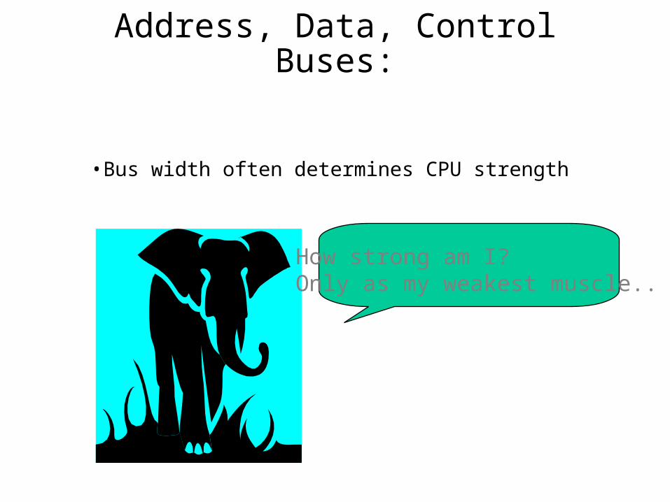
Address, Data, Control Buses:
How strong am I?Only as my weakest muscle..
• Bus width often determines CPU strength
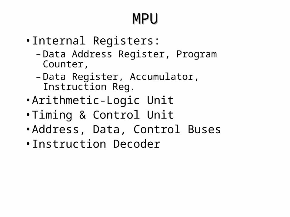
MPUMPU
• Internal Registers:– Data Address Register, Program Counter,– Data Register, Accumulator, Instruction Reg.
• Arithmetic-Logic Unit• Timing & Control Unit• Address, Data, Control Buses• Instruction Decoder
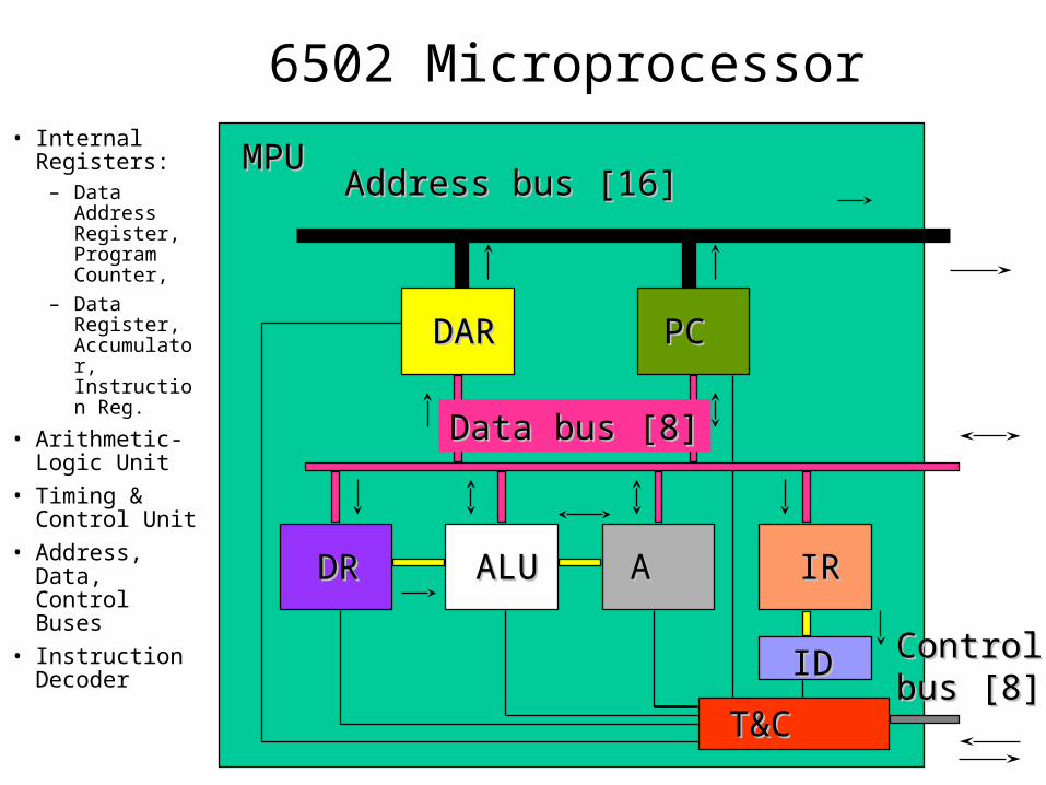
6502 Microprocessor
Address bus [16]Address bus [16]
DARDAR PCPC
DRDR ALUALU AA IRIR
Data bus [8]Data bus [8]
IDID
T&CT&C
ControlControlbus [8]bus [8]
MPUMPU• Internal
Registers:– Data
Address Register, Program Counter,
– Data Register, Accumulator, Instruction Reg.
• Arithmetic-Logic Unit
• Timing & Control Unit
• Address, Data, Control Buses
• Instruction Decoder
Analysis versus Analysis versus DesignDesign
• Analysis– a process of determining the behavior of a given
system / circuit
• Design / Synthesis– a process of going from a formal description /
technical specifications to be met to a system / circuit diagram
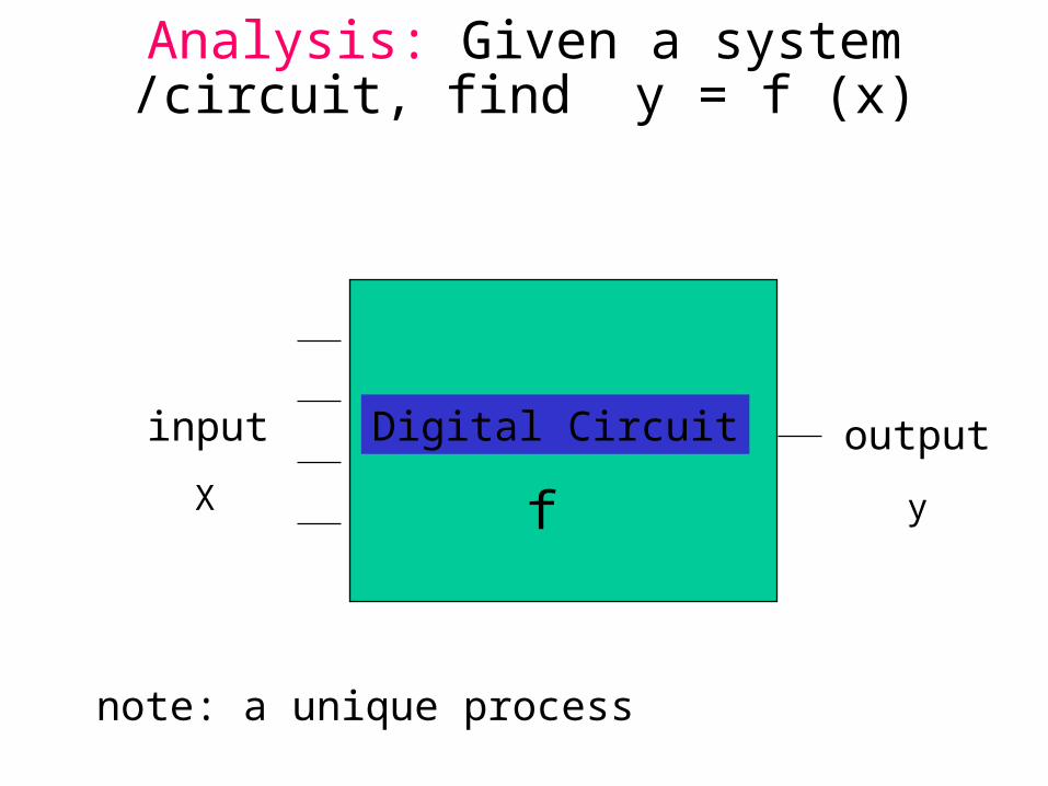
Analysis: Given a system /circuit, find y = f (x)
Digital Circuitinput output
X yf
note: a unique process

Design: Given a specification / behavior of y, design / build system /
circuit f (x)
Digital Circuitinput output
X yf
note : not a unique process
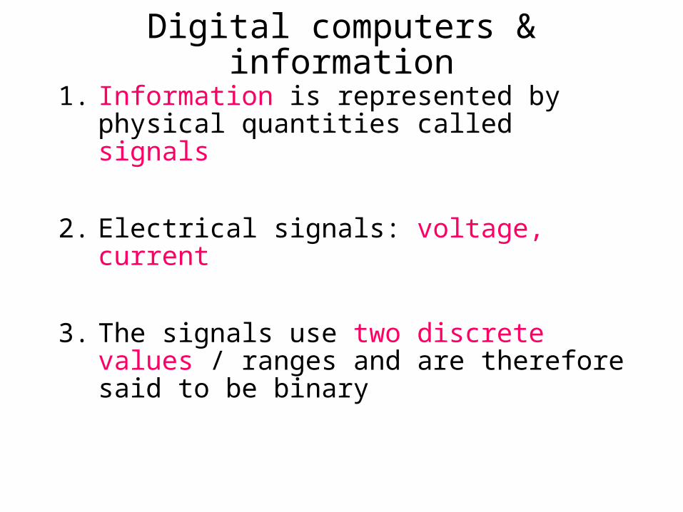
Digital computers & information
1. Information is represented by physical quantities called signals
2. Electrical signals: voltage, current
3. The signals use two discrete values / ranges and are therefore said to be binary
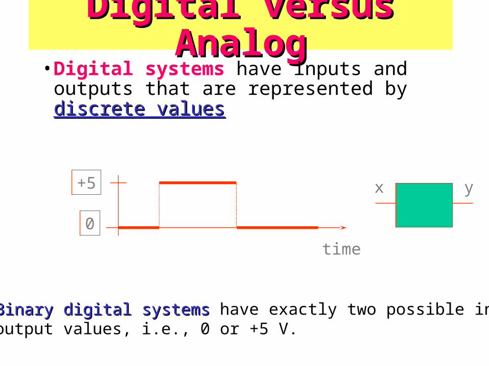
Digital versus AnalogDigital versus Analog• Digital systems have inputs and outputs that
are represented by discrete valuesdiscrete values
+5
0
time
Binary digital systemsBinary digital systems have exactly two possible input / output values, i.e., 0 or +5 V.
x y
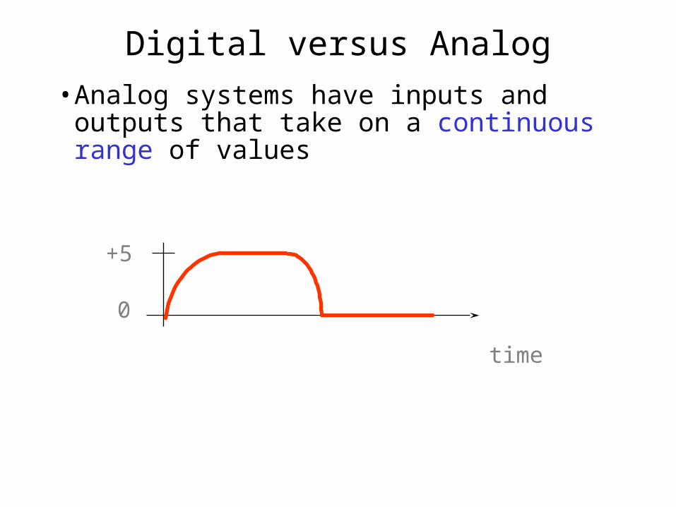
Digital versus Analog
• Analog systems have inputs and outputs that take on a continuous range of values
+5
0
time

Pros & cons of digital vs analog
• Digital systems have inherent ability to deal with electrical signals that have been degraded degraded by transmission through circuits
• The real world operates in an analog fashion-that is continuously; – thus digital systems need interface devices
( sensor, actuators, converters ) to control analog devices
I - Introduction© Copyright 2004, Gaetano Borriello and Randy
H. Katz 16
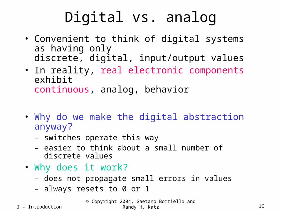
Digital vs. analog
• Convenient to think of digital systems as having onlydiscrete, digital, input/output values
• In reality, real electronic components exhibitcontinuous, analog, behavior
• Why do we make the digital abstraction anyway?– switches operate this way– easier to think about a small number of discrete values
• Why does it work?– does not propagate small errors in values– always resets to 0 or 1

Advantages of Digital Techniques
1. Easy storage of information
2. Accuracy and precision
3. Easier to design
4. Programmability
5. Less affected by noise
6. Easier fabrication processes
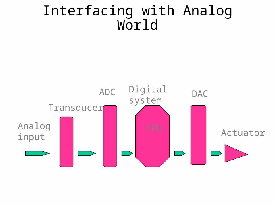
Interfacing with Analog World
Analoginput
Transducer
ADC Digitalsystem
DAC
ActuatorCPU
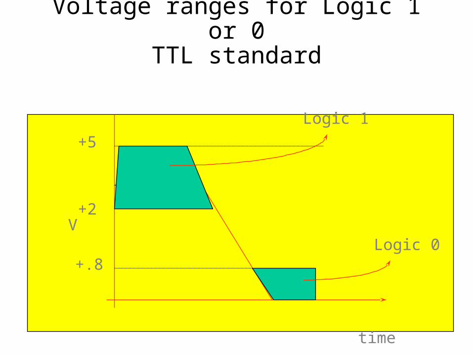
Voltage ranges for Logic 1 or 0TTL standard
+5
Logic 1
Logic 0V
time
+2
+.8
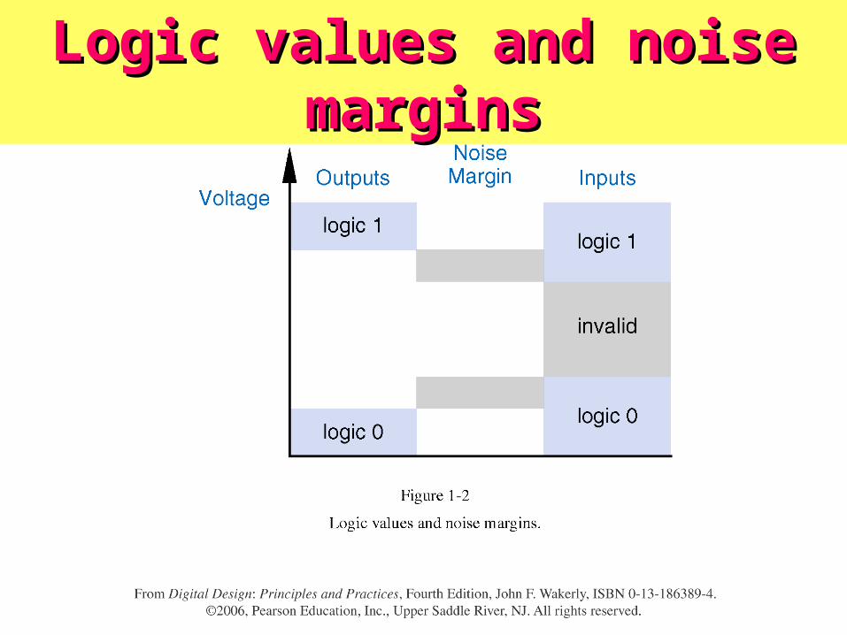
Logic values and noise marginsLogic values and noise margins
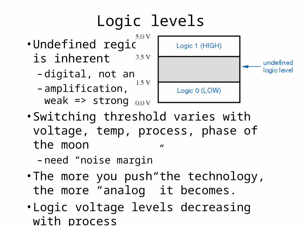
Logic levels
• Undefined regionis inherent– digital, not analog– amplification,
weak => strong
• Switching threshold varies with voltage, temp, process, phase of the moon– need “noise margin”
• The more you push the technology, the more “analog” it becomes.
• Logic voltage levels decreasing with process– 5 -> 3.3 -> 2.5 -> 1.8 V
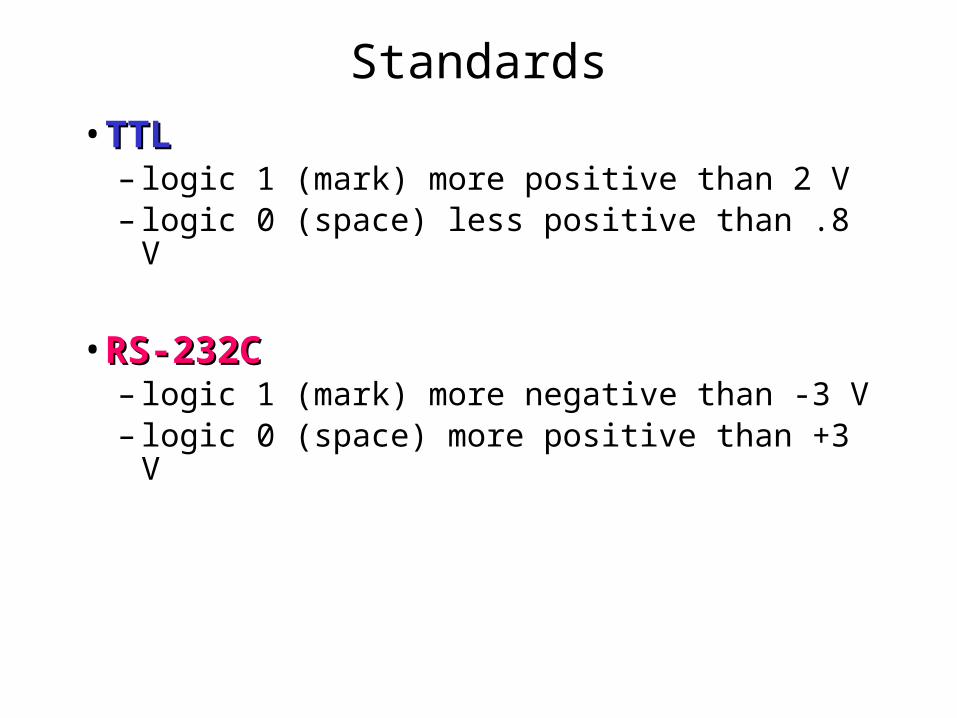
Standards
• TTLTTL– logic 1 (mark) more positive than 2 V– logic 0 (space) less positive than .8 V
• RS-232CRS-232C– logic 1 (mark) more negative than -3 V– logic 0 (space) more positive than +3 V
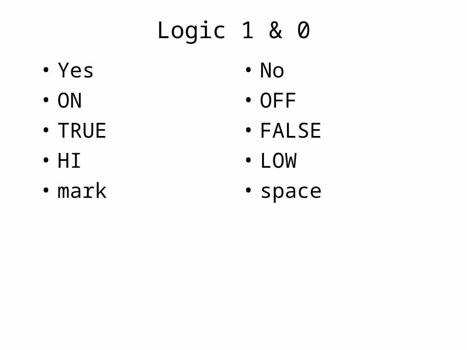
Logic 1 & 0
• Yes
• ON
• TRUE
• HI
• mark
• No
• OFF
• FALSE
• LOW
• space

More on ranges of voltage valuescalled HIGH and LOW
OUTPUT INPUT
4
3
21
H
LVolts
H
L
Note: noise margin & immunity
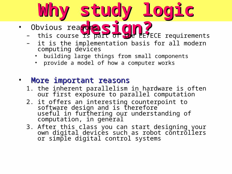
Why study logic design?Why study logic design?• Obvious reasons
– this course is part of the EE/ECE requirements– it is the implementation basis for all modern computing
devices• building large things from small components• provide a model of how a computer works
• More important reasonsMore important reasons1. the inherent parallelism in hardware is often our first
exposure to parallel computation2. it offers an interesting counterpoint to software design and
is therefore useful in furthering our understanding of computation, in general
3. After this class you can start designing your own digital devices such as robot controllers or simple digital control systems
I - Introduction© Copyright 2004, Gaetano Borriello and Randy
H. Katz 26
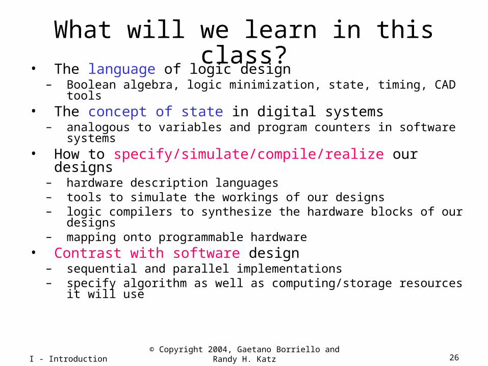
What will we learn in this class?
• The language of logic design– Boolean algebra, logic minimization, state, timing, CAD tools
• The concept of state in digital systems– analogous to variables and program counters in software systems
• How to specify/simulate/compile/realize our designs– hardware description languages– tools to simulate the workings of our designs– logic compilers to synthesize the hardware blocks of our designs– mapping onto programmable hardware
• Contrast with software design– sequential and parallel implementations– specify algorithm as well as computing/storage resources it will
use
I - Introduction© Copyright 2004, Gaetano Borriello and Randy
H. Katz 27
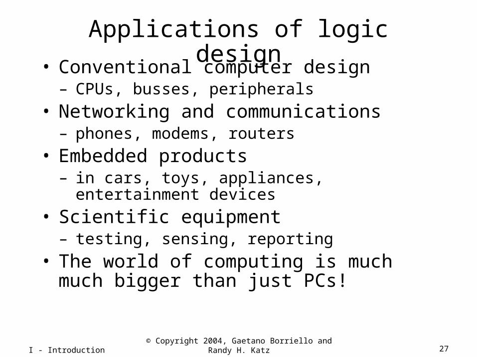
Applications of logic design
• Conventional computer design– CPUs, busses, peripherals
• Networking and communications– phones, modems, routers
• Embedded products– in cars, toys, appliances, entertainment devices
• Scientific equipment– testing, sensing, reporting
• The world of computing is much much bigger than just PCs!
I - Introduction© Copyright 2004, Gaetano Borriello and Randy
H. Katz 28
What is logic design?• What is design?
– given a specification of a problem, come up with a way of solving it choosing appropriately from a collection of available components
– while meeting some criteria for size, cost, power, beauty, elegance, etc.
• What is logic design?– determining the collection of digital logic components to perform
a specified control and/or data manipulation and/or communication function and the interconnections between them
– which logic components to choose? – there are many implementation technologies (e.g., off-the-shelf fixed-function components, programmable devices, transistors on a chip, etc.)
– the design may need to be optimized and/or transformed to meet design constraints
I - Introduction© Copyright 2004, Gaetano Borriello and Randy
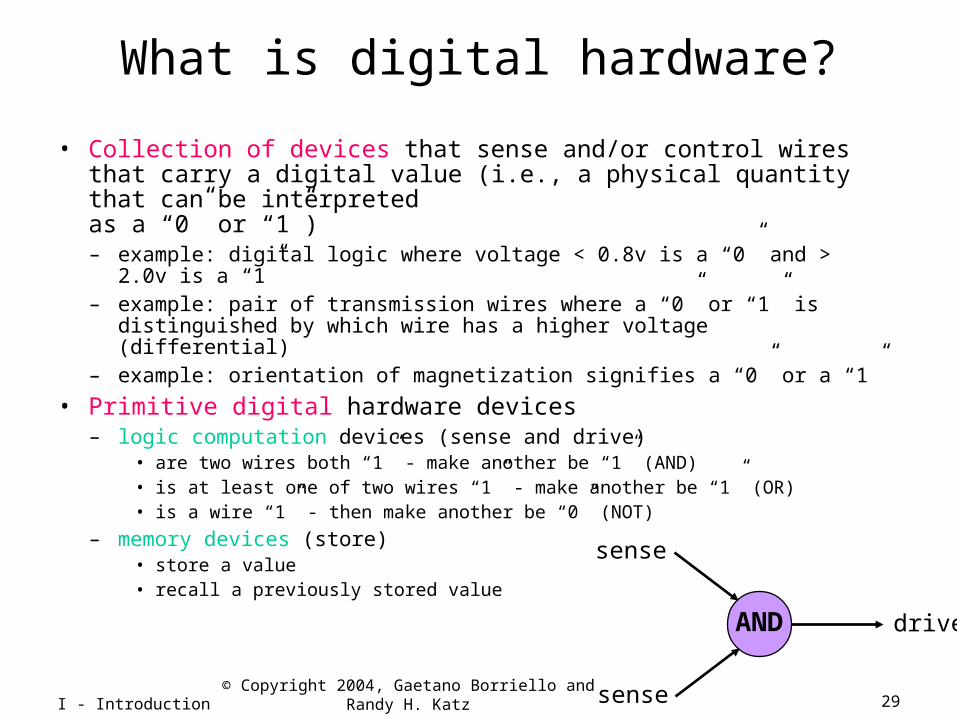
H. Katz 29sense
sense
driveAND
What is digital hardware?
• Collection of devices that sense and/or control wires that carry a digital value (i.e., a physical quantity that can be interpreted as a “0” or “1”)– example: digital logic where voltage < 0.8v is a “0” and > 2.0v is a “1”– example: pair of transmission wires where a “0” or “1” is distinguished
by which wire has a higher voltage (differential)– example: orientation of magnetization signifies a “0” or a “1”
• Primitive digital hardware devices– logic computation devices (sense and drive)
• are two wires both “1” - make another be “1” (AND)• is at least one of two wires “1” - make another be “1” (OR)• is a wire “1” - then make another be “0” (NOT)
– memory devices (store)• store a value• recall a previously stored value

I - Introduction© Copyright 2004, Gaetano Borriello and Randy
H. Katz 30
What is happening now in digital design?
• Important trends in how industry does hardware design– larger and larger designs
– shorter and shorter time to market
– cheaper and cheaper products
• Scale– pervasive use of computer-aided design tools over hand methods
– multiple levels of design representation
• Time – emphasis on abstract design representations
– programmable rather than fixed function components
– automatic synthesis techniques
– importance of sound design methodologies
• Cost– higher levels of integration
– use of simulation to debug designs
– simulate and verify before you build
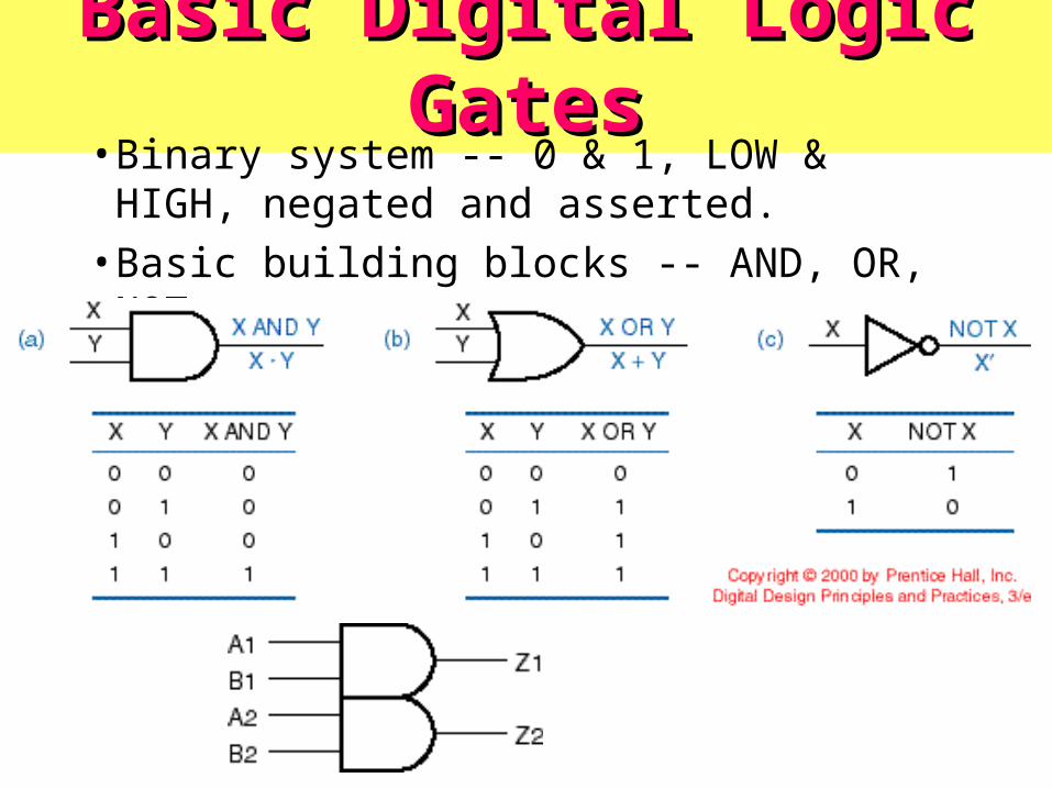
Basic Digital Logic GatesBasic Digital Logic Gates• Binary system -- 0 & 1, LOW & HIGH, negated
and asserted.• Basic building blocks -- AND, OR, NOT
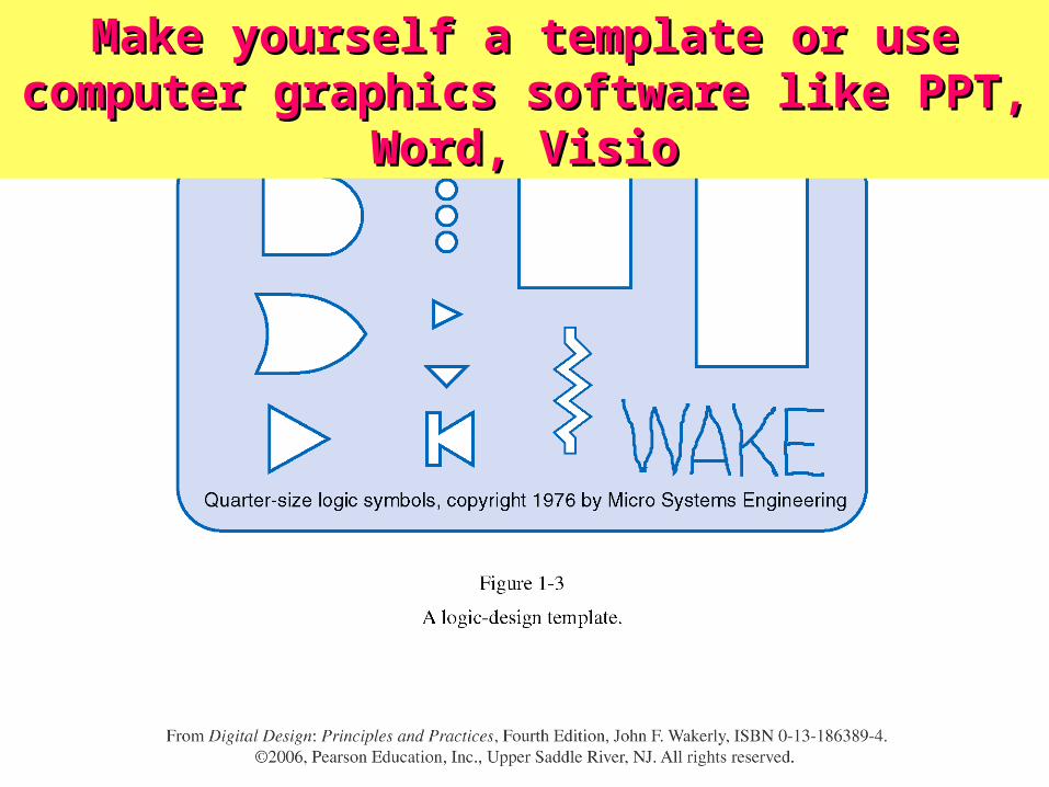
Make yourself a template or use computer graphics Make yourself a template or use computer graphics software like PPT, Word, Visiosoftware like PPT, Word, Visio
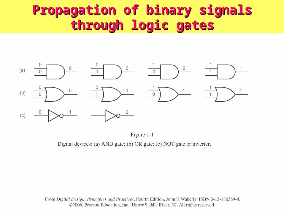
Propagation of binary signals through logic gatesPropagation of binary signals through logic gates
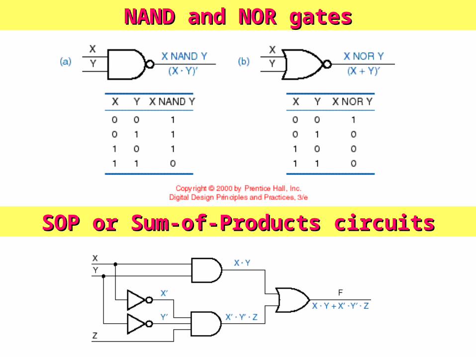
NAND and NOR gatesNAND and NOR gates
SOP or Sum-of-Products circuitsSOP or Sum-of-Products circuits

Packaging of digital circuitsPackaging of digital circuits

Pin diagrams of TTL digital circuitsPin diagrams of TTL digital circuits

PLDs, CPLDs and FPGAs in briefPLDs, CPLDs and FPGAs in brief
I - Introduction© Copyright 2004, Gaetano Borriello and Randy
H. Katz 38
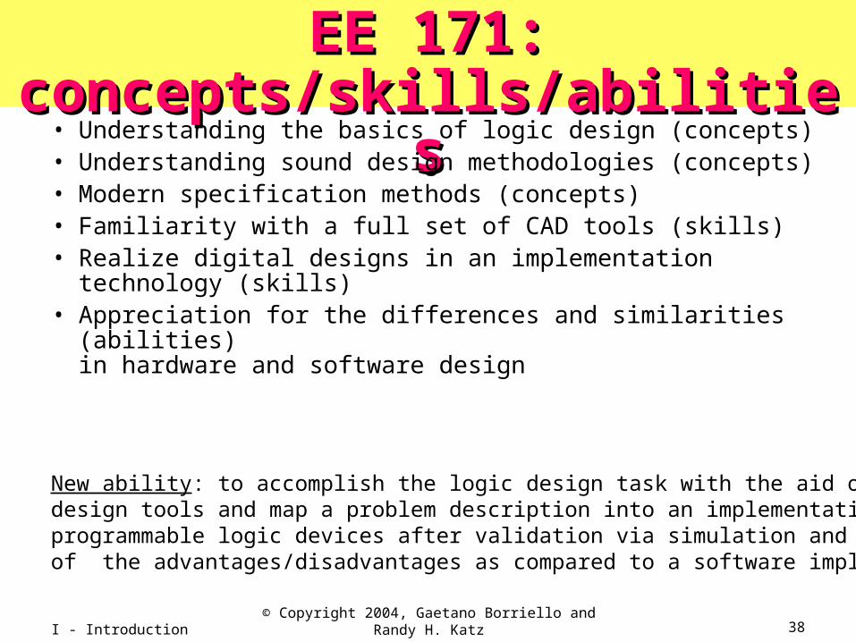
New ability: to accomplish the logic design task with the aid of computer-aideddesign tools and map a problem description into an implementation withprogrammable logic devices after validation via simulation and understandingof the advantages/disadvantages as compared to a software implementation
EE 171: EE 171: concepts/skills/abilitiesconcepts/skills/abilities
• Understanding the basics of logic design (concepts)• Understanding sound design methodologies (concepts)• Modern specification methods (concepts)• Familiarity with a full set of CAD tools (skills)• Realize digital designs in an implementation technology
(skills)• Appreciation for the differences and similarities (abilities)
in hardware and software design
I - Introduction© Copyright 2004, Gaetano Borriello and Randy
H. Katz 39
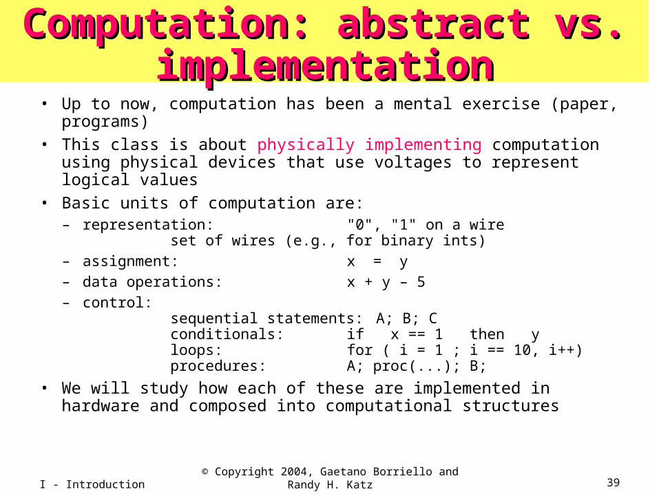
Computation: abstract vs. Computation: abstract vs. implementationimplementation
• Up to now, computation has been a mental exercise (paper, programs)• This class is about physically implementing computation using physical
devices that use voltages to represent logical values• Basic units of computation are:
– representation: "0", "1" on a wireset of wires (e.g., for binary ints)
– assignment: x = y– data operations: x + y – 5– control:
sequential statements: A; B; Cconditionals: if x == 1 then yloops: for ( i = 1 ; i == 10, i++)procedures: A; proc(...); B;
• We will study how each of these are implemented in hardware and composed into computational structures

I - Introduction© Copyright 2004, Gaetano Borriello and Randy
H. Katz 40
close switch (if A is “1” or asserted)and turn on light bulb (Z)
A Z
open switch (if A is “0” or unasserted)and turn off light bulb (Z)
Switches: basic element of Switches: basic element of physical implementationsphysical implementations
• Implementing a simple circuit (arrow shows action if wire changes to “1”):
Z A
AZ
I - Introduction© Copyright 2004, Gaetano Borriello and Randy
H. Katz 41
AND
OR
Z A and B
Z A or B
A B
A
B
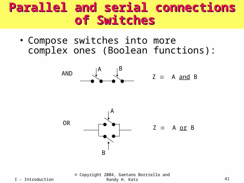
Parallel and serial connections of Parallel and serial connections of Switches Switches
• Compose switches into more complex ones (Boolean functions):
I - Introduction© Copyright 2004, Gaetano Borriello and Randy
H. Katz 42
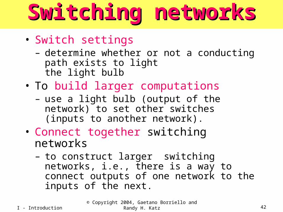
Switching networksSwitching networks• Switch settings
– determine whether or not a conducting path exists to light the light bulb
• To build larger computations– use a light bulb (output of the network) to set other
switches (inputs to another network).
• Connect together switching networks– to construct larger switching networks, i.e., there is
a way to connect outputs of one network to the inputs of the next.
I - Introduction© Copyright 2004, Gaetano Borriello and Randy
H. Katz 43
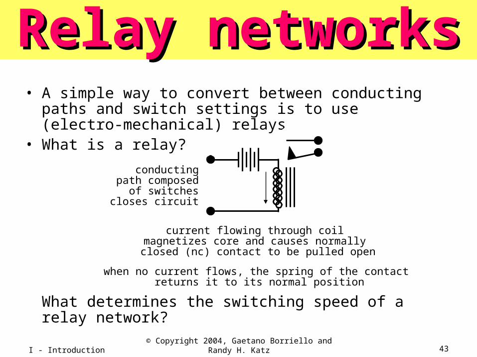
conductingpath composed
of switchescloses circuit
current flowing through coil magnetizes core and causes normally closed (nc) contact to be pulled open
when no current flows, the spring of the contact returns it to its normal position
Relay networksRelay networks• A simple way to convert between conducting paths and
switch settings is to use (electro-mechanical) relays.• What is a relay?
What determines the switching speed of a relay network?
I - Introduction© Copyright 2004, Gaetano Borriello and Randy
H. Katz 44
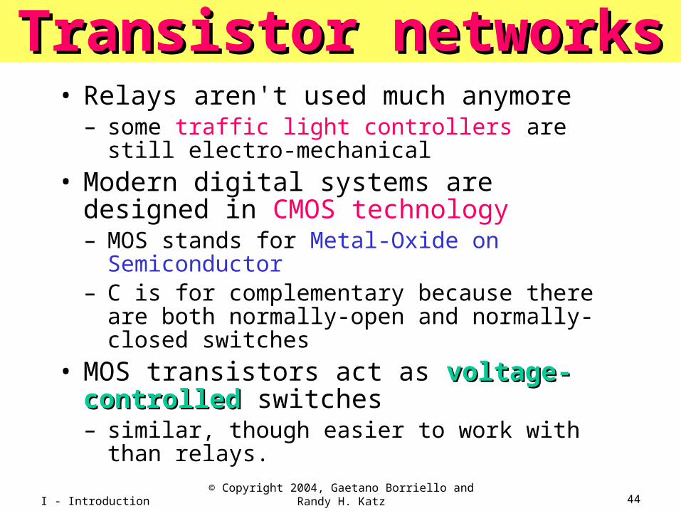
Transistor networksTransistor networks• Relays aren't used much anymore
– some traffic light controllers are still electro-mechanical
• Modern digital systems are designed in CMOS technology– MOS stands for Metal-Oxide on Semiconductor– C is for complementary because there are both
normally-open and normally-closed switches
• MOS transistors act as voltage-controlledvoltage-controlled switches– similar, though easier to work with than relays.
I - Introduction© Copyright 2004, Gaetano Borriello and Randy
H. Katz 45
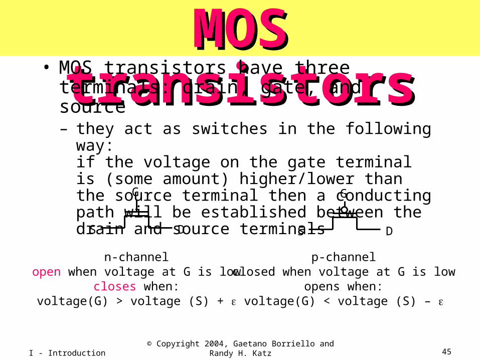
n-channelopen when voltage at G is low
closes when:voltage(G) > voltage (S) +
p-channelclosed when voltage at G is low
opens when:voltage(G) < voltage (S) –
MOS transistorsMOS transistors• MOS transistors have three terminals: drain,
gate, and source– they act as switches in the following way:
if the voltage on the gate terminal is (some amount) higher/lower than the source terminal then a conducting path will be established between the drain and source terminals
G
S D
G
S D

I - Introduction© Copyright 2004, Gaetano Borriello and Randy
H. Katz 46
3v
X
Y 0 volts
x y
3 volts0v
what is the relationship
between x and y?
MOS networksMOS networks
0 volts
3 volts
This explains how MOS inverter worksThis explains how MOS inverter works

I - Introduction© Copyright 2004, Gaetano Borriello and Randy
H. Katz 47
x y z1 z2
0 volts
3 volts
0 volts
3 volts
0 volts
0 volts
3 volts
3 volts
what is the relationship
between x, y and z?
Two input networks: what do you think Two input networks: what do you think are these gates?are these gates?
3v
X Y
0v
Z1
3v
X Y
0v
Z2
3 volts
3 volts
3 volts
0 volts
3 volts
0 volts
0 volts
0 volts
NAND NOR

I - Introduction© Copyright 2004, Gaetano Borriello and Randy
H. Katz 48
Speed of MOS networksSpeed of MOS networks• What influences the speed of CMOSspeed of CMOS
networks?– charging and discharging of voltages on wires and
gates of transistors
• Capacitors hold charge– capacitance is at gates of transistors and wire
material
• Resistors slow movement of electrons– resistance mostly due to transistors
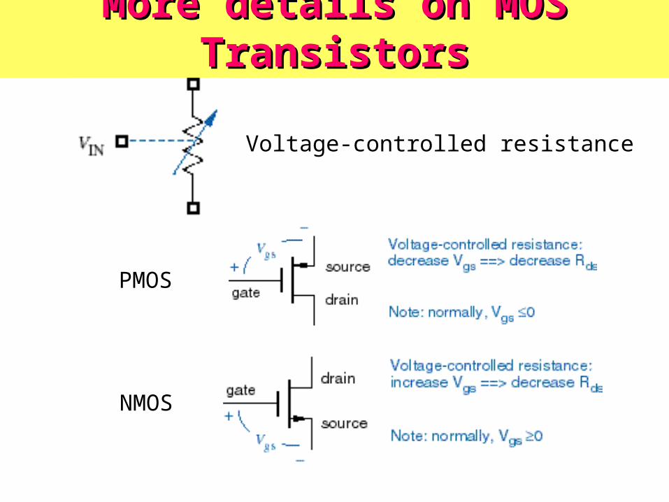
More details on MOS TransistorsMore details on MOS Transistors
NMOS
PMOS
Voltage-controlled resistance
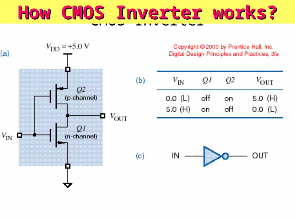
CMOS InverterHow CMOS Inverter works?How CMOS Inverter works?
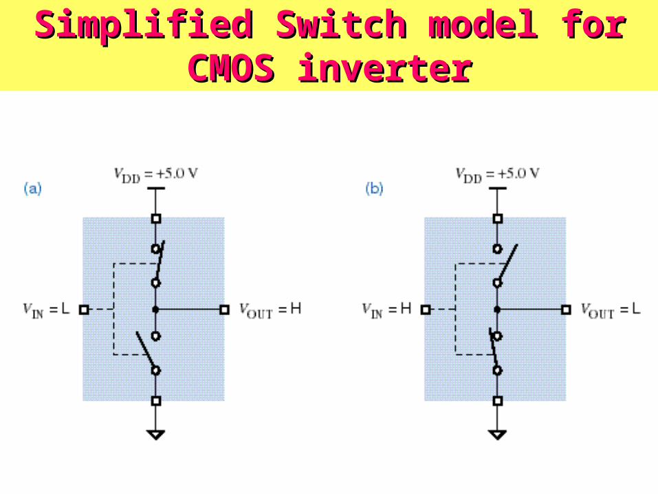
Simplified Switch model for CMOS Simplified Switch model for CMOS inverterinverter
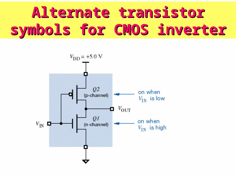
Alternate transistor symbols for Alternate transistor symbols for CMOS inverterCMOS inverter

CMOS Gate Characteristics CMOS Gate Characteristics
• No DC current flowNo DC current flow into MOS gate terminal– However gate has capacitance ==> current required
for switching (CV2f power)
• No current in output structure, except during switching– Both transistors partially on– Power consumption related
to frequency– Slow input-signal rise times
==> more power
• Symmetric output structure ==> equally strong drive in LOW and HIGH states
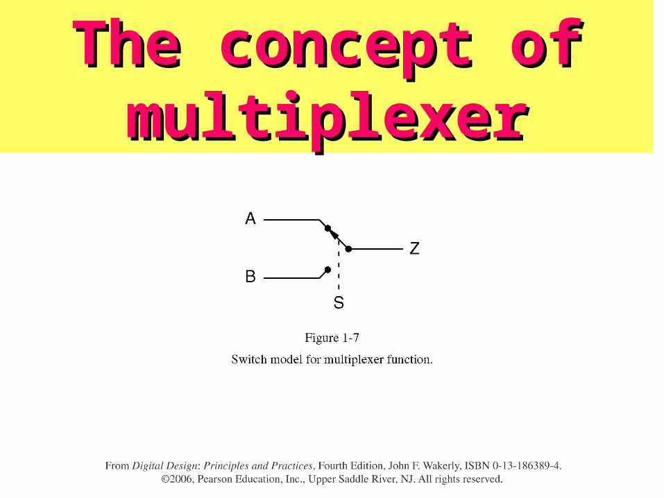
The concept of The concept of multiplexermultiplexer
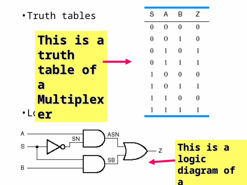
• Truth tables
• Logic diagrams
This is a This is a truth table truth table of a of a MultiplexerMultiplexer
This is a logic This is a logic diagram of a diagram of a MultiplexerMultiplexer
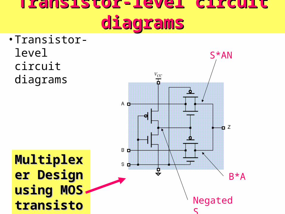
Transistor-level circuit diagramsTransistor-level circuit diagrams
• Transistor-levelcircuit diagrams
Negated S
S*AN
B*A
Multiplexer Multiplexer Design using Design using MOS MOS transistorstransistors

• Prepackaged building blocks, e.g. multiplexer
• Equations: Z = S¢ × A + S × B
A,B,Z have 4 bits each
Package for a 4-bit, 2-word multiplexerPackage for a 4-bit, 2-word multiplexer
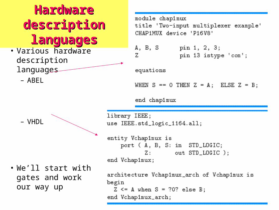
• Various hardware description languages– ABEL
– VHDL
• We’ll start with gates and work our way up
Hardware description Hardware description languageslanguages

Structural style of digital circuits Structural style of digital circuits specificationspecification
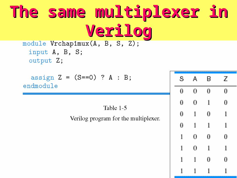
The same multiplexer in VerilogThe same multiplexer in Verilog
I - Introduction© Copyright 2004, Gaetano Borriello and Randy
H. Katz 61
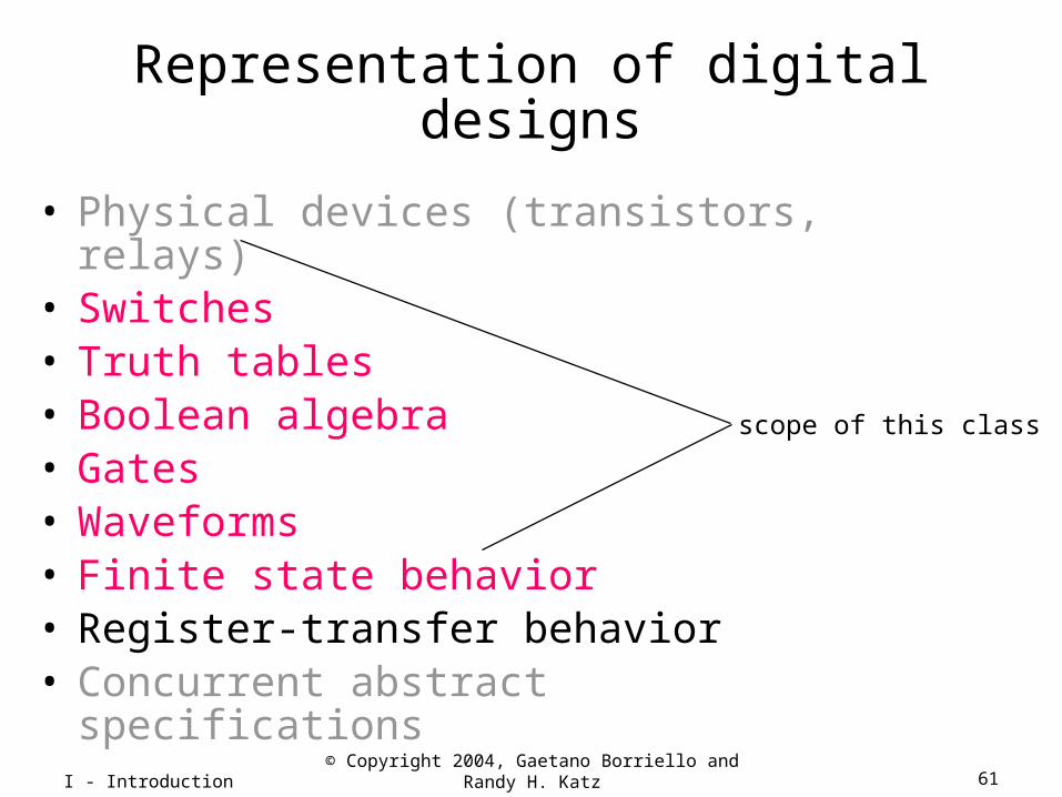
scope of this class
Representation of digital designs
• Physical devices (transistors, relays)• Switches• Truth tables• Boolean algebra• Gates• Waveforms• Finite state behavior• Register-transfer behavior• Concurrent abstract specifications

I - Introduction© Copyright 2004, Gaetano Borriello and Randy
H. Katz 62
Technology State 0 State 1
Relay logic Circuit Open Circuit ClosedCMOS logic 0.0-1.0 volts 2.0-3.0 voltsTransistor transistor logic (TTL) 0.0-0.8 volts 2.0-5.0 voltsFiber Optics Light off Light onDynamic RAM Discharged capacitor Charged capacitorNonvolatile memory (erasable) Trapped electrons No trapped electronsProgrammable ROM Fuse blown Fuse intactBubble memory No magnetic bubble Bubble presentMagnetic disk No flux reversal Flux reversalCompact disc No pit Pit
Mapping from physical world to Mapping from physical world to binary worldbinary world
I - Introduction© Copyright 2004, Gaetano Borriello and Randy
H. Katz 63
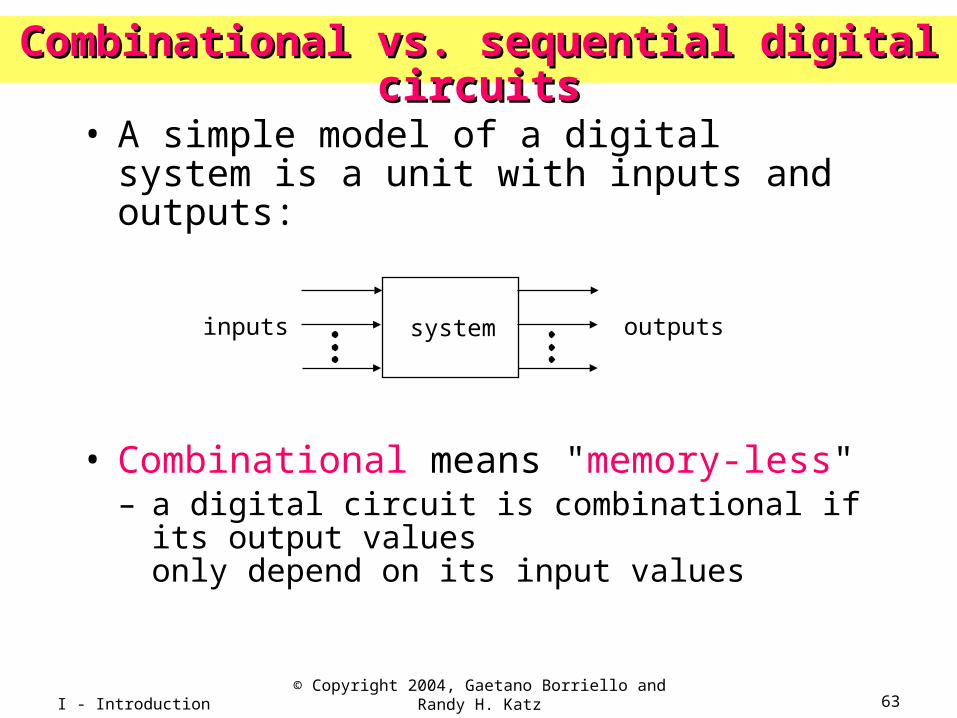
inputs outputssystem
Combinational vs. sequential digital circuitsCombinational vs. sequential digital circuits
• A simple model of a digital system is a unit with inputs and outputs:
• Combinational means "memory-less"– a digital circuit is combinational if its output values
only depend on its input values

I - Introduction© Copyright 2004, Gaetano Borriello and Randy
H. Katz 64
easy to implementwith CMOS transistors(the switches we haveavailable and use most)
Combinational logic networksCombinational logic networks
• Common combinational logic systems have standard symbols called logic gates
– Buffer, NOT
– AND, NAND
– OR, NOR
Z
AB
Z
Z
A
AB
-- EXOR, XNOR, MUX-- EXOR, XNOR, MUX
I - Introduction© Copyright 2004, Gaetano Borriello and Randy
H. Katz 65
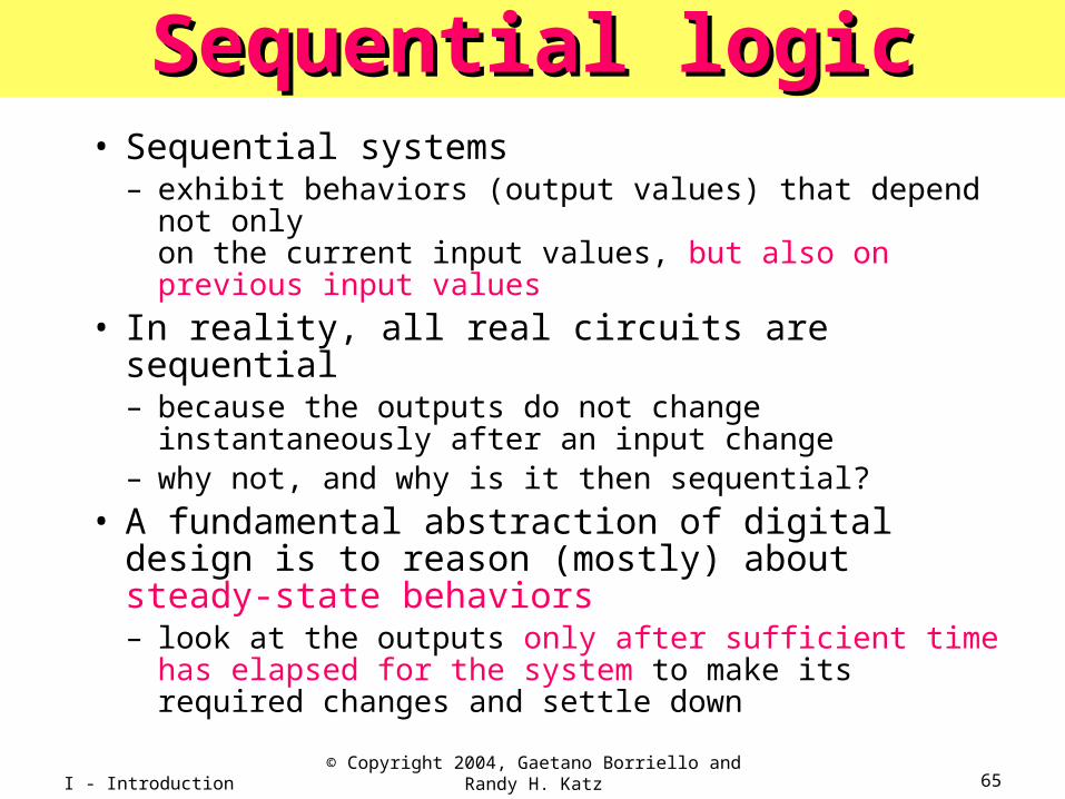
Sequential logicSequential logic• Sequential systems
– exhibit behaviors (output values) that depend not only on the current input values, but also on previous input values
• In reality, all real circuits are sequential– because the outputs do not change instantaneously
after an input change– why not, and why is it then sequential?
• A fundamental abstraction of digital design is to reason (mostly) about steady-state behaviors– look at the outputs only after sufficient time has
elapsed for the system to make its required changes and settle down
I - Introduction© Copyright 2004, Gaetano Borriello and Randy
H. Katz 66
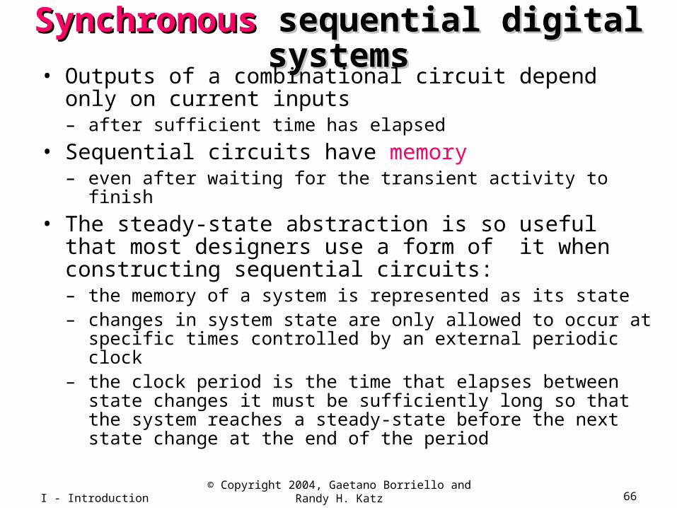
SynchronousSynchronous sequential digital systems sequential digital systems
• Outputs of a combinational circuit depend only on current inputs– after sufficient time has elapsed
• Sequential circuits have memory– even after waiting for the transient activity to finish
• The steady-state abstraction is so useful that most designers use a form of it when constructing sequential circuits:– the memory of a system is represented as its state– changes in system state are only allowed to occur at specific times
controlled by an external periodic clock– the clock period is the time that elapses between state changes it
must be sufficiently long so that the system reaches a steady-state before the next state change at the end of the period

I - Introduction© Copyright 2004, Gaetano Borriello and Randy
H. Katz 67
B
AC
Clock
Example of combinational and Example of combinational and sequential logicsequential logic
• Combinational:– input A, B– wait for clock edge– observe C– wait for another clock edge– observe C again: will stay the same
• Sequential:– input A, B– wait for clock edge– observe C– wait for another clock edge– observe C again: may be different
I - Introduction© Copyright 2004, Gaetano Borriello and Randy
H. Katz 68
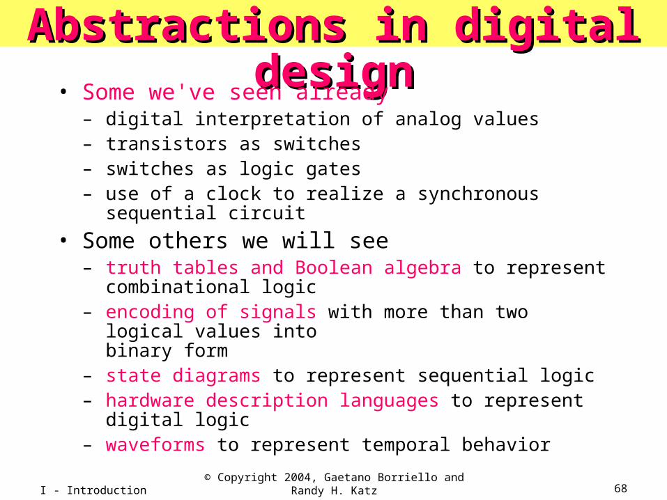
Abstractions in digital designAbstractions in digital design• Some we've seen already
– digital interpretation of analog values– transistors as switches– switches as logic gates– use of a clock to realize a synchronous sequential circuit
• Some others we will see– truth tables and Boolean algebra to represent combinational
logic– encoding of signals with more than two logical values into
binary form– state diagrams to represent sequential logic– hardware description languages to represent digital logic– waveforms to represent temporal behavior
I - Introduction© Copyright 2004, Gaetano Borriello and Randy
H. Katz 69
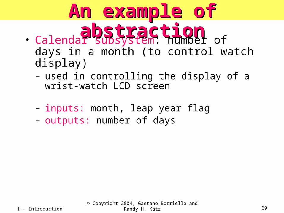
An example of abstractionAn example of abstraction• Calendar subsystem: number of days in a
month (to control watch display)– used in controlling the display of a wrist-watch LCD
screen
– inputs: month, leap year flag– outputs: number of days
I - Introduction© Copyright 2004, Gaetano Borriello and Randy
H. Katz 70
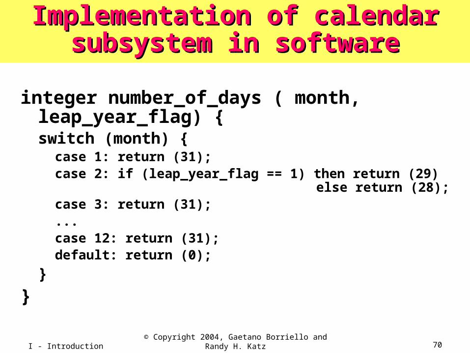
Implementation of calendar Implementation of calendar subsystem in softwaresubsystem in software
integer number_of_days ( month, leap_year_flag) {switch (month) {
case 1: return (31);case 2: if (leap_year_flag == 1) then return (29)
else return (28);case 3: return (31);...case 12: return (31);default: return (0);
}
}
I - Introduction© Copyright 2004, Gaetano Borriello and Randy
H. Katz 71
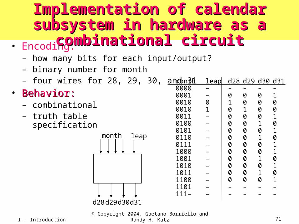
leapmonth
d28d29d30d31
month leap d28 d29 d30 d310000 – – – – – 0001 – 0 0 0 10010 0 1 0 0 00010 1 0 1 0 00011 – 0 0 0 10100 – 0 0 1 00101 – 0 0 0 10110 – 0 0 1 00111 – 0 0 0 11000 – 0 0 0 11001 – 0 0 1 01010 – 0 0 0 11011 – 0 0 1 01100 – 0 0 0 11101 – – – – –111– – – – – –
Implementation as acombinational digital system
• Encoding:– how many bits for each input/output?– binary number for month– four wires for 28, 29, 30, and 31
• Behavior:Behavior:– combinational– truth table
specification
Implementation of calendar subsystem Implementation of calendar subsystem in hardware as a combinational circuitin hardware as a combinational circuit

I - Introduction© Copyright 2004, Gaetano Borriello and Randy
H. Katz 72
symbol for and
symbol for or
symbol for not
Combinational example (cont’d)• Truth-table to logic to switches to gates
– d28 = 1 when month=0010 and leap=0– d28 = m8'•m4'•m2•m1'•leap'
– d31 = 1 when month=0001 or month=0011 or ... month=1100
– d31 = (m8'•m4'•m2'•m1) + (m8'•m4'•m2•m1) + ... (m8•m4•m2'•m1')
– d31 = can we simplify more?
month leap d28 d29 d30 d310001 – 0 0 0 10010 0 1 0 0 00010 1 0 1 0 00011 – 0 0 0 10100 – 0 0 1 0...1100 – 0 0 0 11101 – – – – –111– – – – – –0000 – – – – –

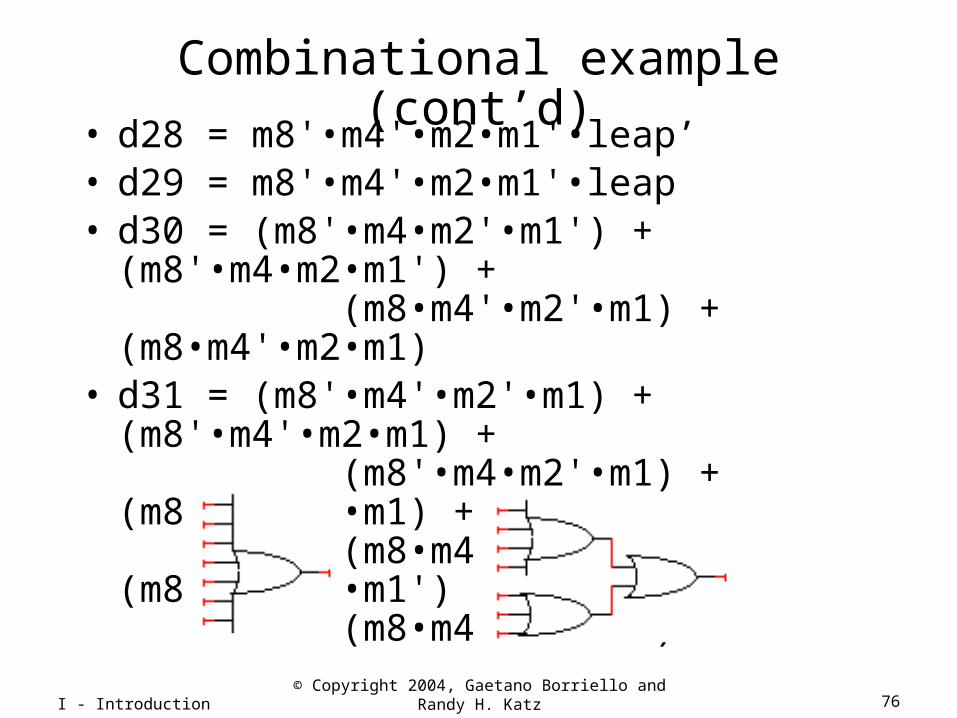
Combinational example (cont’d)
• d28 = m8'•m4'•m2•m1'•leap’• d29 = m8'•m4'•m2•m1'•leap• d30 = (m8'•m4•m2'•m1') + (m8'•m4•m2•m1') +
(m8•m4'•m2'•m1) + (m8•m4'•m2•m1) = (m8'•m4•m1') + (m8•m4'•m1)
• d31 = (m8'•m4'•m2'•m1) + (m8'•m4'•m2•m1) + (m8'•m4•m2'•m1) + (m8'•m4•m2•m1) + (m8•m4'•m2'•m1') + (m8•m4'•m2•m1') + (m8•m4•m2'•m1')
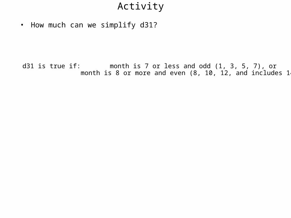
Activity
• How much can we simplify d31?
d31 is true if:month is 7 or less and odd (1, 3, 5, 7), ormonth is 8 or more and even (8, 10, 12, and includes 14)
d31 is true if: m8 is 0 and m1 is 1, or m8 is 1 and m1 is 0
d31 = m8’m1 + m8m1’
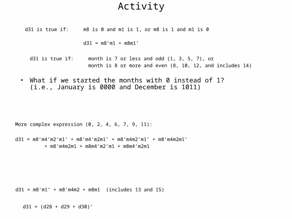
Activity
• What if we started the months with 0 instead of 1?(i.e., January is 0000 and December is 1011)
d31 is true if: month is 7 or less and odd (1, 3, 5, 7), ormonth is 8 or more and even (8, 10, 12, and includes 14)
d31 is true if: m8 is 0 and m1 is 1, or m8 is 1 and m1 is 0
d31 = m8’m1 + m8m1’
d31 = m8’m1’ + m8’m4m2 + m8m1 (includes 13 and 15)
d31 = (d28 + d29 + d30)’
More complex expression (0, 2, 4, 6, 7, 9, 11):
d31 = m8’m4’m2’m1’ + m8’m4’m2m1’ + m8’m4m2’m1’ + m8’m4m2m1’+ m8’m4m2m1 + m8m4’m2’m1 + m8m4’m2m1
I - Introduction© Copyright 2004, Gaetano Borriello and Randy
H. Katz 76
Combinational example (cont’d)
• d28 = m8'•m4'•m2•m1'•leap’• d29 = m8'•m4'•m2•m1'•leap• d30 = (m8'•m4•m2'•m1') + (m8'•m4•m2•m1') +
(m8•m4'•m2'•m1) + (m8•m4'•m2•m1)• d31 = (m8'•m4'•m2'•m1) + (m8'•m4'•m2•m1) +
(m8'•m4•m2'•m1) + (m8'•m4•m2•m1) + (m8•m4'•m2'•m4') + (m8•m4'•m2•m1') +
(m8•m4•m2'•m1')
I - Introduction© Copyright 2004, Gaetano Borriello and Randy
H. Katz 77
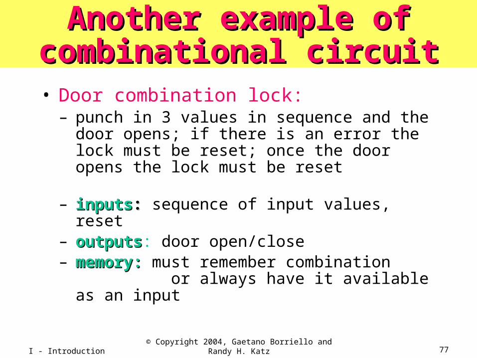
Another example of Another example of combinational circuitcombinational circuit
• Door combination lock:– punch in 3 values in sequence and the door opens;
if there is an error the lock must be reset; once the door opens the lock must be reset
– inputsinputs:: sequence of input values, reset– outputsoutputs: door open/close– memory:memory: must remember combination
or always have it available as an input
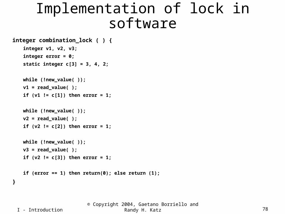
I - Introduction© Copyright 2004, Gaetano Borriello and Randy
H. Katz 78
Implementation of lock in software
integer combination_lock ( ) {
integer v1, v2, v3;
integer error = 0;
static integer c[3] = 3, 4, 2;
while (!new_value( ));
v1 = read_value( );
if (v1 != c[1]) then error = 1;
while (!new_value( ));
v2 = read_value( );
if (v2 != c[2]) then error = 1;
while (!new_value( ));
v3 = read_value( );
if (v2 != c[3]) then error = 1;
if (error == 1) then return(0); else return (1);
}
I - Introduction© Copyright 2004, Gaetano Borriello and Randy
H. Katz 79
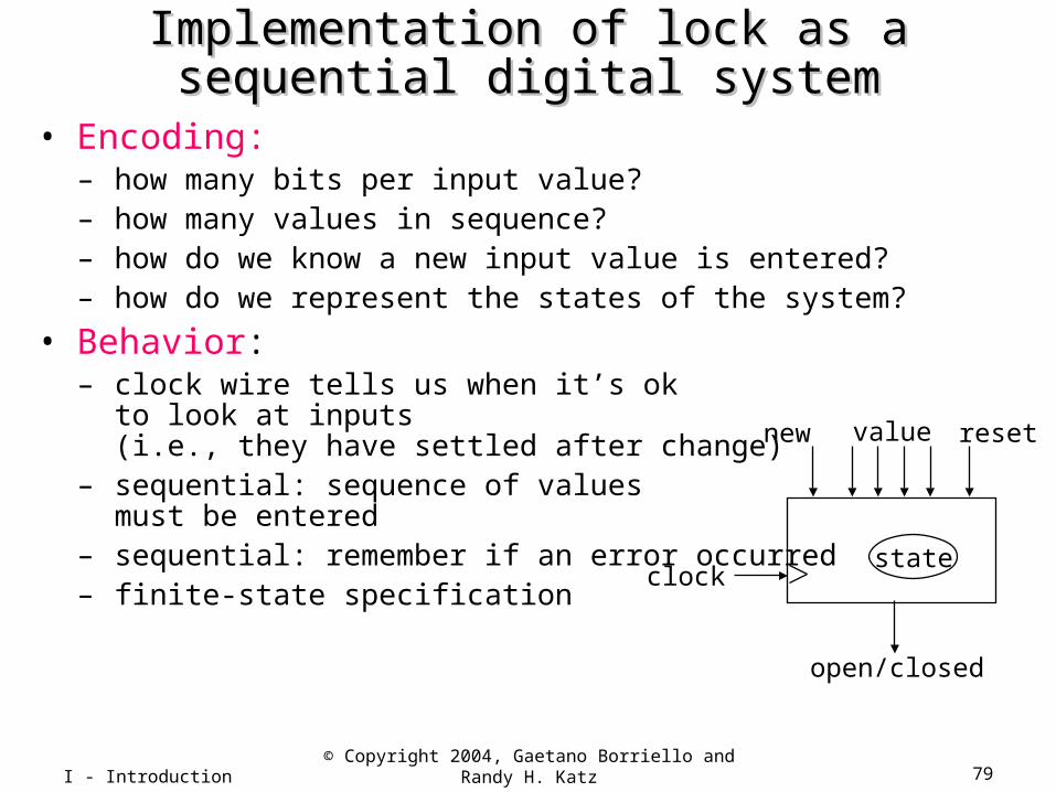
Implementation of lock as a sequential digital Implementation of lock as a sequential digital systemsystem
• Encoding:– how many bits per input value?– how many values in sequence?– how do we know a new input value is entered?– how do we represent the states of the system?
• Behavior:– clock wire tells us when it’s ok
to look at inputs(i.e., they have settled after change)
– sequential: sequence of valuesmust be entered
– sequential: remember if an error occurred– finite-state specification
resetvalue
open/closed
new
clockstate
I - Introduction© Copyright 2004, Gaetano Borriello and Randy
H. Katz 80
C2!=value& new
C3!=value& new
reset
not newnot newnot new
closed
S1
closedC1=value
& new
S2
closedC2=value
& new
S3
C3=value& new
OPEN
open
C1!=value& new
closed
ERR
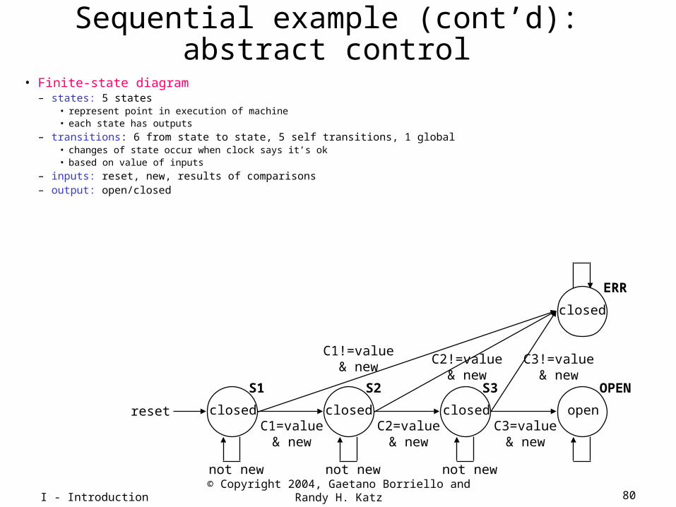
Sequential example (cont’d):abstract control
• Finite-state diagram– states: 5 states
• represent point in execution of machine• each state has outputs
– transitions: 6 from state to state, 5 self transitions, 1 global• changes of state occur when clock says it’s ok• based on value of inputs
– inputs: reset, new, results of comparisons– output: open/closed
I - Introduction© Copyright 2004, Gaetano Borriello and Randy
H. Katz 81
reset
open/closed
new
C1 C2 C3
comparator
value
equal
multiplexer
equal
controllermux control
clock
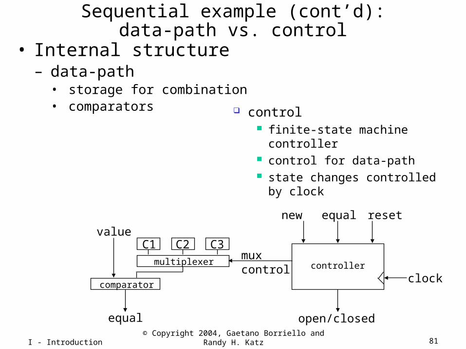
Sequential example (cont’d):data-path vs. control
• Internal structure– data-path
• storage for combination• comparators control
finite-state machine controller control for data-path state changes controlled by clock
I - Introduction© Copyright 2004, Gaetano Borriello and Randy
H. Katz 82
closed
closedmux=C1reset equal
& new
not equal& new
not equal& new
not equal& new
not newnot newnot new
S1 S2 S3 OPEN
ERR
closedmux=C2 equal
& new
closedmux=C3 equal
& new
open
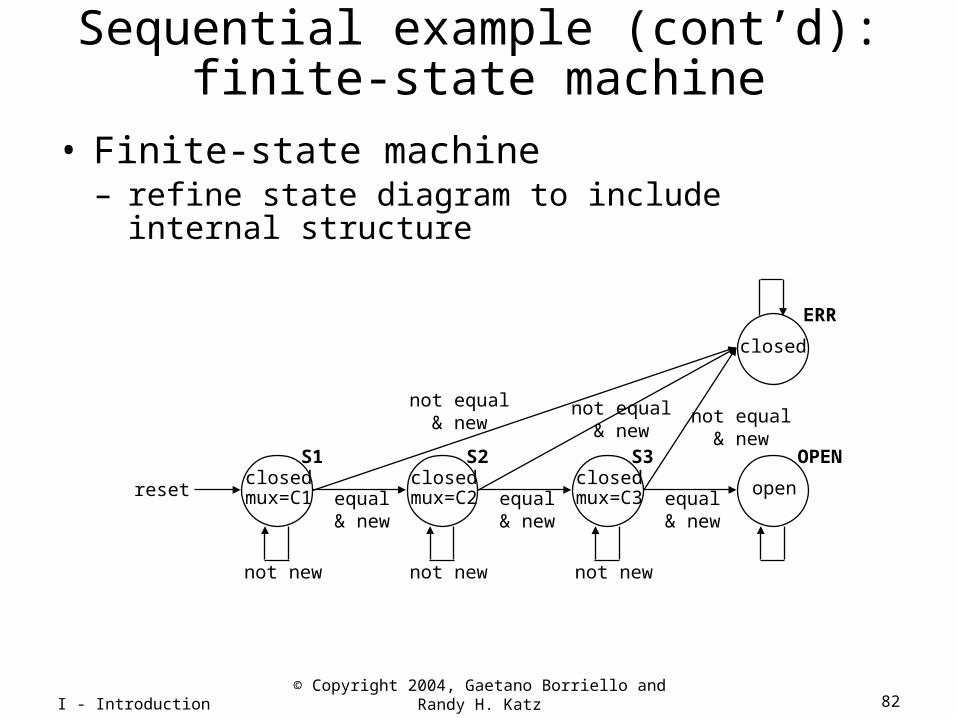
Sequential example (cont’d):finite-state machine
• Finite-state machine– refine state diagram to include internal structure
I - Introduction© Copyright 2004, Gaetano Borriello and Randy
H. Katz 83
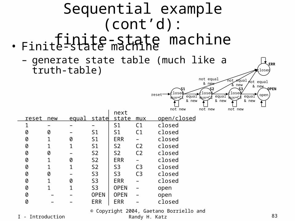
reset new equal state state mux open/closed1 – – – S1 C1 closed0 0 – S1 S1 C1 closed0 1 0 S1 ERR – closed0 1 1 S1 S2 C2 closed0 0 – S2 S2 C2 closed0 1 0 S2 ERR – closed0 1 1 S2 S3 C3 closed0 0 – S3 S3 C3 closed0 1 0 S3 ERR – closed0 1 1 S3 OPEN – open 0 – – OPEN OPEN – open0 – – ERR ERR – closed
next
Sequential example (cont’d):finite-state machine
• Finite-state machine– generate state table (much like a truth-table)
closed
closedmux=C1
reset equal& new
not equal& new
not equal& new
not equal& new
not newnot newnot new
S1 S2 S3 OPEN
ERR
closedmux=C2 equal
& new
closedmux=C3 equal
& new
open
I - Introduction© Copyright 2004, Gaetano Borriello and Randy
H. Katz 84
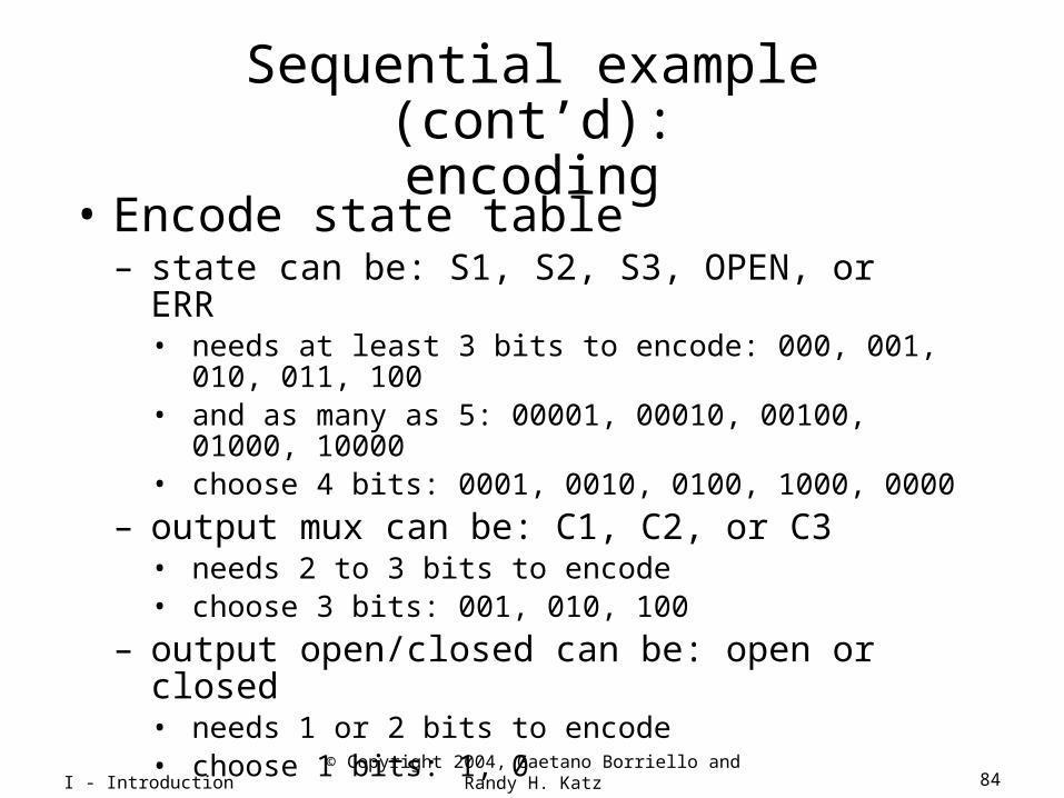
Sequential example (cont’d):encoding
• Encode state table– state can be: S1, S2, S3, OPEN, or ERR
• needs at least 3 bits to encode: 000, 001, 010, 011, 100• and as many as 5: 00001, 00010, 00100, 01000, 10000• choose 4 bits: 0001, 0010, 0100, 1000, 0000
– output mux can be: C1, C2, or C3• needs 2 to 3 bits to encode• choose 3 bits: 001, 010, 100
– output open/closed can be: open or closed• needs 1 or 2 bits to encode• choose 1 bits: 1, 0
I - Introduction© Copyright 2004, Gaetano Borriello and Randy
H. Katz 85
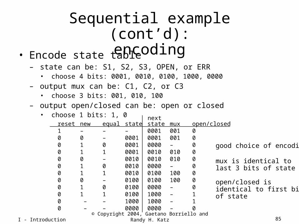
good choice of encoding!
mux is identical to last 3 bits of state
open/closed isidentical to first bitof state
Sequential example (cont’d):encoding
• Encode state table– state can be: S1, S2, S3, OPEN, or ERR
• choose 4 bits: 0001, 0010, 0100, 1000, 0000
– output mux can be: C1, C2, or C3• choose 3 bits: 001, 010, 100
– output open/closed can be: open or closed• choose 1 bits: 1, 0
reset new equal state state mux open/closed1 – – – 0001 001 0 0 0 – 0001 0001 001 00 1 0 0001 0000 – 00 1 1 0001 0010 010 0 0 0 – 0010 0010 010 00 1 0 0010 0000 – 00 1 1 0010 0100 100 0 0 0 – 0100 0100 100 00 1 0 0100 0000 – 00 1 1 0100 1000 – 1 0 – – 1000 1000 – 10 – – 0000 0000 – 0
next
I - Introduction© Copyright 2004, Gaetano Borriello and Randy
H. Katz 86
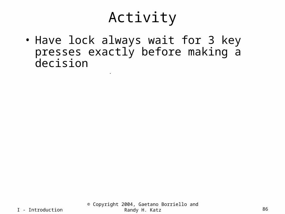
Activity
• Have lock always wait for 3 key presses exactly before making a decision– remove reset
not equal& new
not equal& new
closedmux=C1 equal
& new
not newnot newnot new
S1 S2 S3 OPENclosed
mux=C2 equal& new
closedmux=C3 equal
& new
open
not equal& new
closed
E2
not new not new
closed
E3new closed
ERRnew
I - Introduction© Copyright 2004, Gaetano Borriello and Randy
H. Katz 87
reset
open/closed
new equal
controllermux control
clock
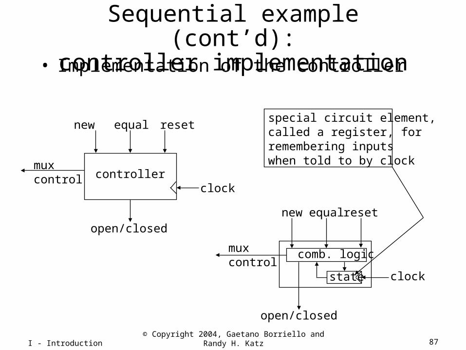
reset
open/closed
new equal
mux control
clock
comb. logic
state
special circuit element, called a register, for remembering inputswhen told to by clock
Sequential example (cont’d):controller implementation
• Implementation of the controller
I - Introduction© Copyright 2004, Gaetano Borriello and Randy
H. Katz 88
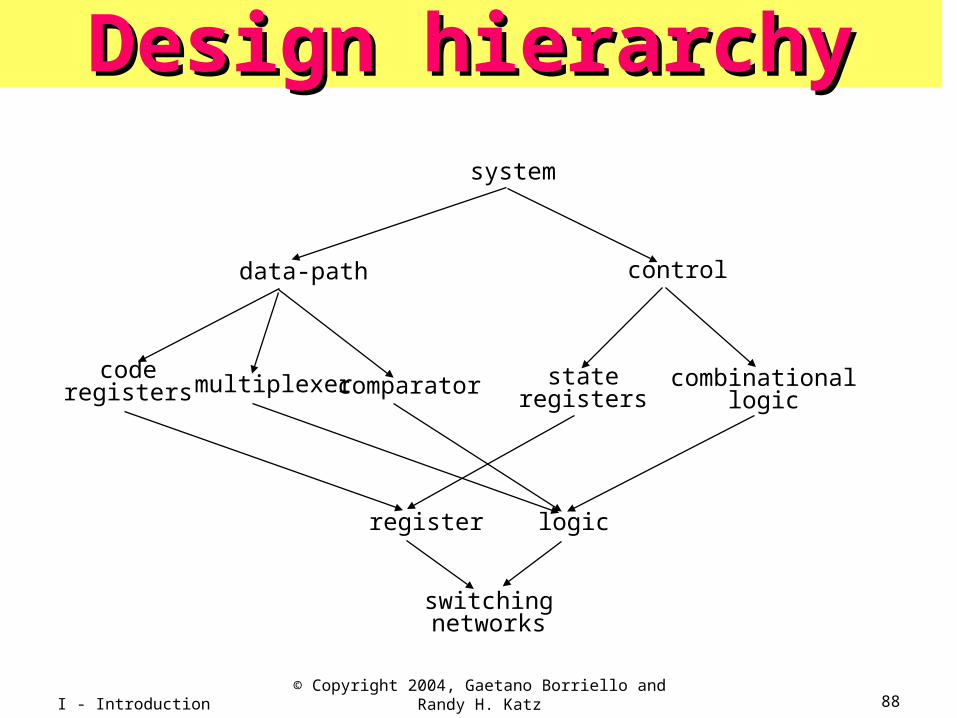
system
data-path control
stateregisters
combinationallogic
multiplexer comparatorcode
registers
register logic
switchingnetworks
Design hierarchyDesign hierarchy
I - Introduction© Copyright 2004, Gaetano Borriello and Randy
H. Katz 89
SummarySummary• That was what the entire course is about
– converting solutions to problems into combinational and sequential networks effectively organizing the design hierarchically
– doing so with a modern set of design tools that lets us handle large designs effectively
– taking advantage of optimization opportunities
• Now lets do it again– this time we'll take nine weeks instead of one

Number SystemsNumber Systems• Stone Age: knots, some stone marks• Roman Empire: more systematic notation I, II,
III, IV, V, VI, VII.VIII, IX, X, C, D, M• Concept of zero by
– Maya- I century, Hindu-V century
• Positional-value systems: decimal, binary, octal, etc..
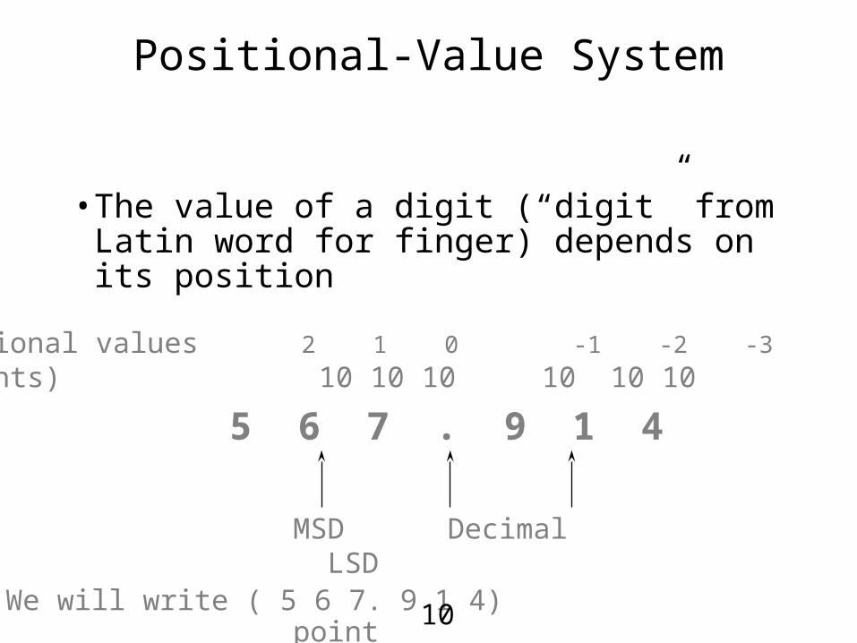
Positional-Value System
• The value of a digit (“digit” from Latin word for finger) depends on its position
5 6 7 . 9 1 4
MSD Decimal LSD point
Positional values 2 1 0 -1 -2 -3
(weights) 10 10 10 10 10 10
We will write ( 5 6 7. 9 1 4)10
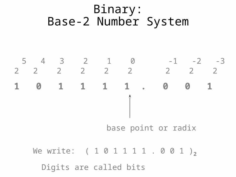
Binary:Base-2 Number System
1 0 1 1 1 1 . 0 0 1
2 2 2 2 2 2 2 2 2 5 4 3 2 1 0 -1 -2 -3
We write: ( 1 0 1 1 1 1 . 0 0 1 )2
base point or radix
Digits are called bits

Conversion ( ) I ( )10
• express number as a power series in I, and add all terms using decimal addition
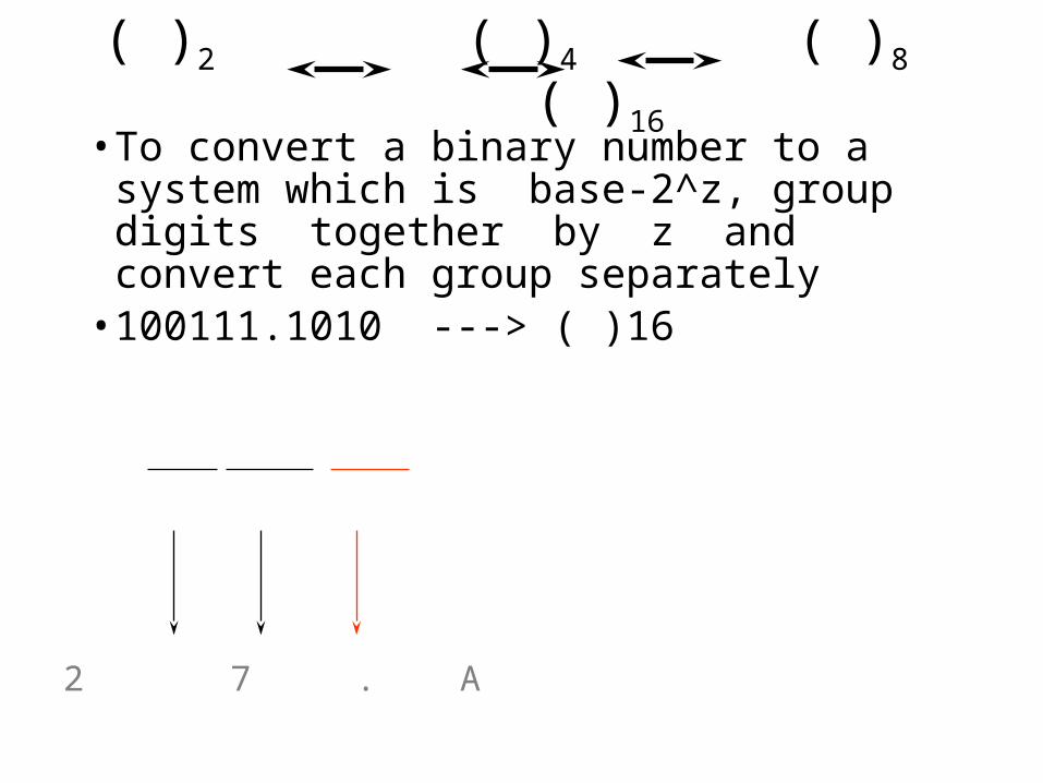
( )2 ( )4 ( )8 ( )16
• To convert a binary number to a system which is base-2^z, group digits together by z and convert each group separately
• 100111.1010 ---> ( )16
2 7 . A
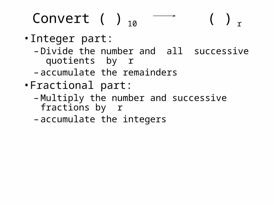
Convert ( ) 10 ( ) r
• Integer part:– Divide the number and all successive quotients
by r– accumulate the remainders
• Fractional part:– Multiply the number and successive fractions by r – accumulate the integers
Modified from John Wakerly, Katz
and Gapinski
Introduction, Logic Circuits