Embed Size (px)
Citation preview


DISCLAIMER Alliance Semiconductor Corporation reserves the right to make changes to its products or specifications at any time, without notice, in order to improve design or performance and to supply the best possible product. Alliance Semiconductor does not assume any responsibility for use of any circuitry described other than the circuitry embodied in an Alliance Semiconductor product. The Company makes no representations that circuitry described herein is free from patent infringement or other rights of third parties which may result from its use. No license is granted by implication or otherwise under any patent, patent rights or other rights, of Alliance Semiconductor Corporation.
LIFE SUPPORT POLICY Alliance Semiconductor Corporation products are not authorized for use as critical components in life support devices or systems unless a specific written agreement pertaining to such intended use is executed between the manufacturer and an officer of Alliance Semiconductor. 1. Life support devices or systems are devices or systems which (a) are intended for surgical implant into the body or (b) support or sustain life and whose failure to perform, when properly used in accordance with instructions for use provided in the labeling, can be reasonably expected to result in a significant injury to the user. 2. A critical component is any components of a life support device or system whose failure to perform can be reasonably expected to cause the failure of the life support device or system, or to affect its safety or effectiveness.
©Copyright 2004. All rights reserved
NTD™ is a trademark of Alliance Semiconductor Corporation. HyperTransport™ is a trademark of the HyperTransport Technology Consortium.

www.alsc.com Product Guide 2004 1 Notice: The information in this document is subject to change without notice.
Table of Contents ANALOG AND MIXED SIGNAL PRODUCTS ................................................................................ 3
ANALOG AND MIXED SIGNAL PRODUCTS ......................................................................................... 4 CLOCK AND TIMING PRODUCTS ...................................................................................................... 5
Clock and Timing Product Selector Guide Alpha-Numeric Listing.......................................... 6 Clock and Timing Product Selector Guide Function and Configuration Listing ...................... 9 Zero Delay Buffers (ZDB) and Specialty Clock Management Cross Reference Guide........ 12 EMI Reduction Products Cross Reference Guide................................................................. 13
POWER AND SYSTEMS MANAGEMENT PRODUCTS.......................................................................... 14 CPU Supervisor Product Selector Guide .............................................................................. 15 CPU Supervisor Cross Reference Guide.............................................................................. 22
SYSTEM SOLUTIONS PRODUCTS............................................................................................. 27 CONNECTIVITY............................................................................................................................. 29
HyperTransport™ Bridges Product Selector Guide .............................................................. 29 AS90L10204 HyperTransport™-to-PCI/PCI-X Bridge .......................................................... 30 AS90L10208 HyperTransport™-to-PCI/PCI-X Bridge .......................................................... 31 JTAG Controllers Product Selector Guide ............................................................................ 32 AS91L1001 JTAG Test Controller......................................................................................... 33 AS91L1002 JTAG Test Sequencer....................................................................................... 34 AS91L1003U 3-Port JTAG Gateway..................................................................................... 35 AS91L1006BU 6-Port JTAG Gateway .................................................................................. 36
NETWORKING .............................................................................................................................. 37 RPR Controllers Product Selector Guide.............................................................................. 37 AS95L210x Family of Resilient Packet Ring Controllers ...................................................... 38
MEMORY PRODUCTS.................................................................................................................. 43 SRAM PRODUCTS....................................................................................................................... 44
Synchronous SRAM.............................................................................................................. 45 Asynchronous SRAM ............................................................................................................ 49 Synchronous SRAM Cross Reference Guide ....................................................................... 51 Fast Asynchronous SRAM Cross Reference Guide ............................................................. 56 Synchronous Dual Port SRAM Cross Reference Guide....................................................... 58

2 Product Guide 2004 www.alsc.com Notice: The information in this document is subject to change without notice.
www.alsc.com Product Guide 2004 3 Notice: The information in this document is subject to change without notice.
ANALOG AND MIXED SIGNAL PRODUCTS

4 Product Guide 2004 www.alsc.com Notice: The information in this document is subject to change without notice.
Analog and Mixed Signal Products Alliance Semiconductor is a worldwide supplier of Analog and Mixed Signal Products in two main categories: Power and Systems Management, and Clock and Timing.
• The Power and Systems Management Portfolio includes CPU Supervisor Products. These include products that feature POR (Power On Reset), WDT (Watch Dog Timers), LVS (Low Voltage Sense), BB (Battery Backup), brownout detect and control, and many more system and device level key functions.
• The Clock and Timing Portfolio includes Frequency Synthesizers and Generators, Multipliers, Zero Delay Buffers, Distribution and Fan-out buffers. The EMI Reduction family of devices, a sub-segment of Clock and Timing, are made up of Frequency Synthesizer and Generators which are widely used in many designs today to reduce radiated emissions towards regulatory compliance. The EMI reduction family is noted for low cost, very low power consumption, very small package size options, and overall timing accuracy and performance.
Fabricated in Low Voltage CMOS technologies, the Analog and Mixed Signal Product portfolio offers a full range of coverage, functions, options, and configurations, that provide flexibility in design and low cost.
Power-On Reset Application
ASM 809
VDD
uP
RESET
XtalOSC
FreqDivide
FBKDivider
PD Filter VCO DIV
MODPD
XIN/CLKIN
XOUT
REF_OUT
EMI ClockSynthesizer
MOD_OUT
LF (ext loop filter)
GND GND

www.alsc.com Product Guide 2004 5 Notice: The information in this document is subject to change without notice.
Clock and Timing Products Alliance Semiconductor provides in-depth coverage and support in Clock Management with cost effective, low power, Clock and Timing solutions that cater to the requirements for PC/Data processing applications and handhelds, high resolution LCD displays, DDR memory modules, consumer applications (MP3 players/recorders, games, etc.), networking, wireless, mobile applications and others. The Clock Management Solution family encompasses Clock and Frequency Generators, Frequency Multipliers, Zero Delay Buffers, and specific specialty solutions. High precision frequency multipliers provide 2x or 4x outputs of the input frequency up to 312 MHz, with higher frequencies to be offered in the near future. The depth of modulation, the profile (sinusoidal, triangular, non-linear), type of modulation and direction (center or down) are selectable from these Clock and Timing products. In addition, both modulated and unmodulated outputs are available. Many of the devices (single, dual and triple PLL based designs) feature a selection of output frequency derived from the input reference, along with the depth of modulation, type of modulation profile, and frequency of modulation through programming via I2C. A broad family of Zero Delay Buffers (ZDB) provide multiple low skew outputs of an input clock suitable for clock distribution applications, such as clocks to multiple PCI slots in a PC motherboard or SDRAM bank clocks. Available in 1:5 and 1:9 configurations with internal feedback or 1:4 and 1:8 configurations with external feedback, these Zero Delay Buffers provide relative skew among various outputs under controlled load conditions. Various drive options are also available to support one or two 50-ohm transmission lines. Clock and Timing products are designed to work with 2.5V, 3.3V, and 5V applications. Clock and Timing devices are found in applications such as workstations, servers, RAID arrays, notebook PCs, LCD high-resolution displays, PDA and hand held devices, automotive electronics, battery-driven entertainment systems, and others.
6 Product Guide 2004 www.alsc.com Notice: The information in this document is subject to change without notice.
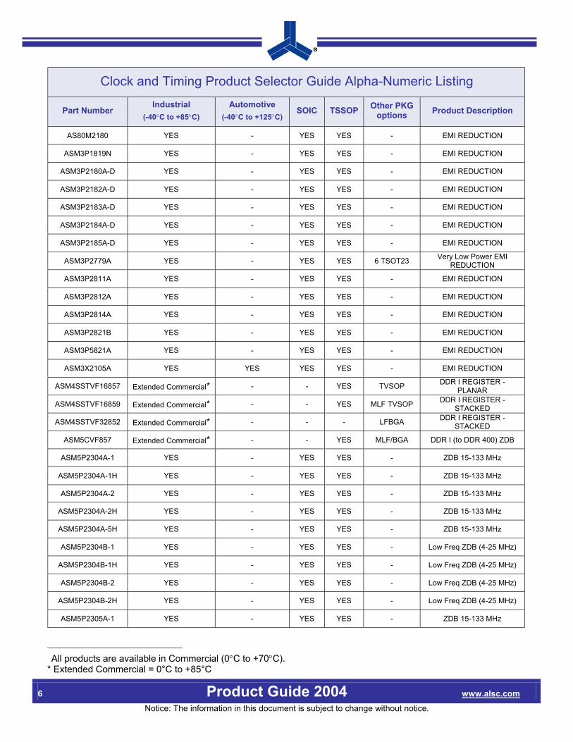
Clock and Timing Product Selector Guide Alpha-Numeric Listing
Part Number Industrial
(-40°C to +85°C) Automotive
(-40°C to +125°C) SOIC TSSOP Other PKG
options Product Description
AS80M2180 YES - YES YES - EMI REDUCTION
ASM3P1819N YES - YES YES - EMI REDUCTION
ASM3P2180A-D YES - YES YES - EMI REDUCTION
ASM3P2182A-D YES - YES YES - EMI REDUCTION
ASM3P2183A-D YES - YES YES - EMI REDUCTION
ASM3P2184A-D YES - YES YES - EMI REDUCTION
ASM3P2185A-D YES - YES YES - EMI REDUCTION
ASM3P2779A YES - YES YES 6 TSOT23 Very Low Power EMI REDUCTION
ASM3P2811A YES - YES YES - EMI REDUCTION
ASM3P2812A YES - YES YES - EMI REDUCTION
ASM3P2814A YES - YES YES - EMI REDUCTION
ASM3P2821B YES - YES YES - EMI REDUCTION
ASM3P5821A YES - YES YES - EMI REDUCTION
ASM3X2105A YES YES YES YES - EMI REDUCTION
ASM4SSTVF16857 Extended Commercial* - - YES TVSOP DDR I REGISTER - PLANAR
ASM4SSTVF16859 Extended Commercial* - - YES MLF TVSOP DDR I REGISTER - STACKED
ASM4SSTVF32852 Extended Commercial* - - - LFBGA DDR I REGISTER - STACKED
ASM5CVF857 Extended Commercial* - - YES MLF/BGA DDR I (to DDR 400) ZDB
ASM5P2304A-1 YES - YES YES - ZDB 15-133 MHz
ASM5P2304A-1H YES - YES YES - ZDB 15-133 MHz
ASM5P2304A-2 YES - YES YES - ZDB 15-133 MHz
ASM5P2304A-2H YES - YES YES - ZDB 15-133 MHz
ASM5P2304A-5H YES - YES YES - ZDB 15-133 MHz
ASM5P2304B-1 YES - YES YES - Low Freq ZDB (4-25 MHz)
ASM5P2304B-1H YES - YES YES - Low Freq ZDB (4-25 MHz)
ASM5P2304B-2 YES - YES YES - Low Freq ZDB (4-25 MHz)
ASM5P2304B-2H YES - YES YES - Low Freq ZDB (4-25 MHz)
ASM5P2305A-1 YES - YES YES - ZDB 15-133 MHz
All products are available in Commercial (0°C to +70°C). * Extended Commercial = 0°C to +85°C

www.alsc.com Product Guide 2004 7 Notice: The information in this document is subject to change without notice.
Clock and Timing Product Selector Guide Alpha-Numeric Listing
Part Number Industrial
(-40°C to +85°C) Automotive
(-40°C to +125°C) SOIC TSSOP Other PKG
options Product Description
ASM5P2305A-1H YES - YES YES - ZDB 15-133 MHz
ASM5P2308A-1 YES - YES YES - ZDB 15-133 MHz
ASM5P2308A-1H YES - YES YES - ZDB 15-133 MHz
ASM5P2308A-2 YES - YES YES - ZDB 15-133 MHz
ASM5P2308A-3 YES - YES YES - ZDB 15-133 MHz
ASM5P2308A-4 YES - YES YES - ZDB 15-133 MHz
ASM5P2308A-5H YES - YES YES - ZDB 15-133 MHz
ASM5P2309A-1 YES - YES YES - ZDB 15-133 MHz
ASM5P2309A-1H YES - YES YES - ZDB 15-133 MHz
ASM5P23S04A-1 YES - YES YES - ZDB 15-133 MHz
ASM5P23S04A-1H YES - YES YES - ZDB 15-133 MHz
ASM5P23S04A-2 YES - YES YES - ZDB 15-133 MHz
ASM5P23S04A-2H YES - YES YES - ZDB 15-133 MHz
ASM5P23S04A-5H YES - YES YES - ZDB 15-133 MHz
ASM5P23S05A-1 YES - YES YES - ZDB 15-133 MHz
ASM5P23S05A-1H YES - YES YES - ZDB 15-133 MHz
ASM5P23S08A-1 YES - YES YES - ZDB 15-133 MHz
ASM5P23S08A-1H YES - YES YES - ZDB 15-133 MHz
ASM5P23S08A-2 YES - YES YES - ZDB 15-133 MHz
ASM5P23S08A-3 YES - YES YES - ZDB 15-133 MHz
ASM5P23S08A-4 YES - YES YES - ZDB 15-133 MHz
ASM5P23S08A-5H YES - YES YES - ZDB 15-133 MHz
ASM5P23S09A-1 YES - YES YES - ZDB 15-133 MHz
ASM5P23S09A-1H YES - YES YES - ZDB 15-133 MHz
L2042A (Low Voltage) YES - YES YES - EMI REDUCTION
P1707A YES - YES YES - EMI REDUCTION
P1708C YES - YES YES - EMI REDUCTION
P1817A-B YES - YES YES - EMI REDUCTION
P1819A-B YES - YES YES - EMI REDUCTION
All products are available in Commercial (0°C to +70°C).

8 Product Guide 2004 www.alsc.com Notice: The information in this document is subject to change without notice.
Clock and Timing Product Selector Guide Alpha-Numeric Listing
Part Number Industrial
(-40°C to +85°C) Automotive
(-40°C to +125°C) SOIC TSSOP Other PKG
options Product Description
P2005A YES YES YES YES - EMI REDUCTION
P2005S YES YES YES YES - EMI REDUCTION
P2008A YES - YES YES - EMI REDUCTION
P2010A YES YES YES YES - EMI REDUCTION
P2027A YES - YES YES - EMI REDUCTION
P2040A YES - YES YES - EMI REDUCTION
P2040C YES - YES YES - EMI REDUCTION
P2041A YES - YES YES - EMI REDUCTION
P2042A YES - YES YES - EMI REDUCTION
P2082A YES - YES YES - FREQUENCY MULTIPLIER
P2084A YES - YES YES - FREQUENCY MULTIPLIER
P2160A YES - YES YES - EMI REDUCTION
P2681A YES - YES YES - EMI REDUCTION
P2779A YES - YES YES - EMI REDUCTION
P2781A YES - YES YES - EMI REDUCTION
P2782A YES - YES YES - EMI REDUCTION
P2784A YES - YES YES - EMI REDUCTION
P2811A YES - YES YES - EMI REDUCTION
P2812A YES - YES YES - EMI REDUCTION
P2814A YES - YES YES - EMI REDUCTION
All products are available in Commercial (0°C to +70°C).

www.alsc.com Product Guide 2004 9 Notice: The information in this document is subject to change without notice.
Clock and Timing Product Selector Guide Function and Configuration Listing
Part Number Frequency
Range (Fin) in MHz
Fout_MAX in MHz
Output Frequency
Deviation (%) Reference
Output ModOut Scaling
Xtal Osc
Supply Voltage Package
Input Frequency Range 6 MHz to 210 MHz
AS80M2180 6-30 30 -1.25% or 4.0% - 1X YES 3.0 to 3.6 8 SOIC 8 TSSOP
ASM3P1819N 20-40 40 -1.25% YES 1X YES 3.0 to 3.6 8 SOIC 8 TSSOP
ASM3P2180A-D 6-36 36 +/-0.625 to -3.5% - 1X - 3.0 to 3.6 8 SOIC 8 TSSOP
ASM3P2182A-D 25-210 210 +/-0.13 to +/-1.24% - 1X - 3.0 to 3.6 8 SOIC
8 TSSOP
ASM3P2183A-D 6-103 103 +/-0.625 to -3.6% - 1X YES 3.0 to 3.6 8 SOIC 8 TSSOP
ASM3P2184A-D 10-40 40 +/-0.625 to -3.5% - 1X YES 3.0 to 3.6 8 SOIC 8 TSSOP
ASM3P2185A-D 25-50 50 +/-0.625 to -1.25% - 1X - 3.0 to 3.6 8 SOIC
8 TSSOP
ASM3P2779A 15-30 38 +/-1% - 1X YES 3.0 to 3.6 8 SOIC 8 TSSOP
ASM3P2811A 10-40 40 +/-0.625 to -3.5% - 1X YES 3.0 to 3.6 8 SOIC 8 TSSOP
ASM3P2812A 10-40 80 +/-0.625 to -3.5% - 2X YES 3.0 to 3.6 8 SOIC 8 TSSOP
ASM3P2814A 10-40 160 +/-0.625 to -3.5% - 4X YES 3.0 to 3.6 8 SOIC 8 TSSOP
ASM3P2821B 15-27 27 -2.5% YES 1X - 3.0 to 3.6 8 SOIC 8 TSSOP
ASM3P5821A 20-40 34 -1.5% - 1X YES 3.0 to 3.6 8 SOIC 8 TSSOP
ASM3X2105A 6-10 10 +/-1% - 1X, ½X YES 3.0 to 3.6 8 SOIC 8 TSSOP
P1817A-B 10-32 32 +/-1.25 to +/-1.50% YES 1X YES 3.0 to 3.6 8 SOIC
8 TSSOP
P1819A-B 20-40 40 +/-0.625 to -3.5% - 1X YES 3.0 to 3.6 8 SOIC 8 TSSOP
P2005A 8-32 32 +/-1.0 to +/-3.0% - 1X, ½X YES 3.0 to 3.6 8 SOIC 8 TSSOP
P2005S 8-32 32 +/-0.6 to +/-1.8% - 1X, ½X YES 3.0 to 3.6 8 SOIC 8 TSSOP
P2008A 4-32 32 +/-0.8 to +/-3.2% YES 1X, ½X YES 2.9 to 5.5 8 SOIC 8 TSSOP
P2010A 10-35 35 +/-1.25 to +/-2.5% - 1X YES 3.0 to 3.6 8 SOIC
8 TSSOP
P2027A 10-30 30 +/-0.2 to +/-0.6% - 1X YES 3.0 to 3.8 8 SOIC 8 TSSOP
P2041A 25-60 60 +/-0.50 to +/-2.50% - 1X - 2.7 to 5.5 8 SOIC
8 TSSOP
P2681A 6-20 20 +/-0.4 to +/-5% - 1X, ½X YES 3.0 to 3.6 8 SOIC 8 TSSOP
P2811A-B 10-40 40 +/-0.625 to -3.5% - 1X YES 3.0 to 3.6 8 SOIC 8 TSSOP
P2812A-B 10-40 80 +/-0.625 to -3.5% - 2X YES 3.0 to 3.6 8 SOIC 8 TSSOP
P2814A-B 10-40 160 +/-0.625 to -3.5% - 4X YES 3.0 to 3.6 8 SOIC 8 TSSOP
Input Frequency Range 30 MHz to 175 MHz
L2042A 30-75 75 +/-0.50 to +/-2.00% - 1X - 2.25 to
3.7 8 SOIC
8 TSSOP
P1708C 60-175 175 +/-0.25 to +/-2.00% - 1X - 3.0 to 3.6 8 SOIC
8 TSSOP
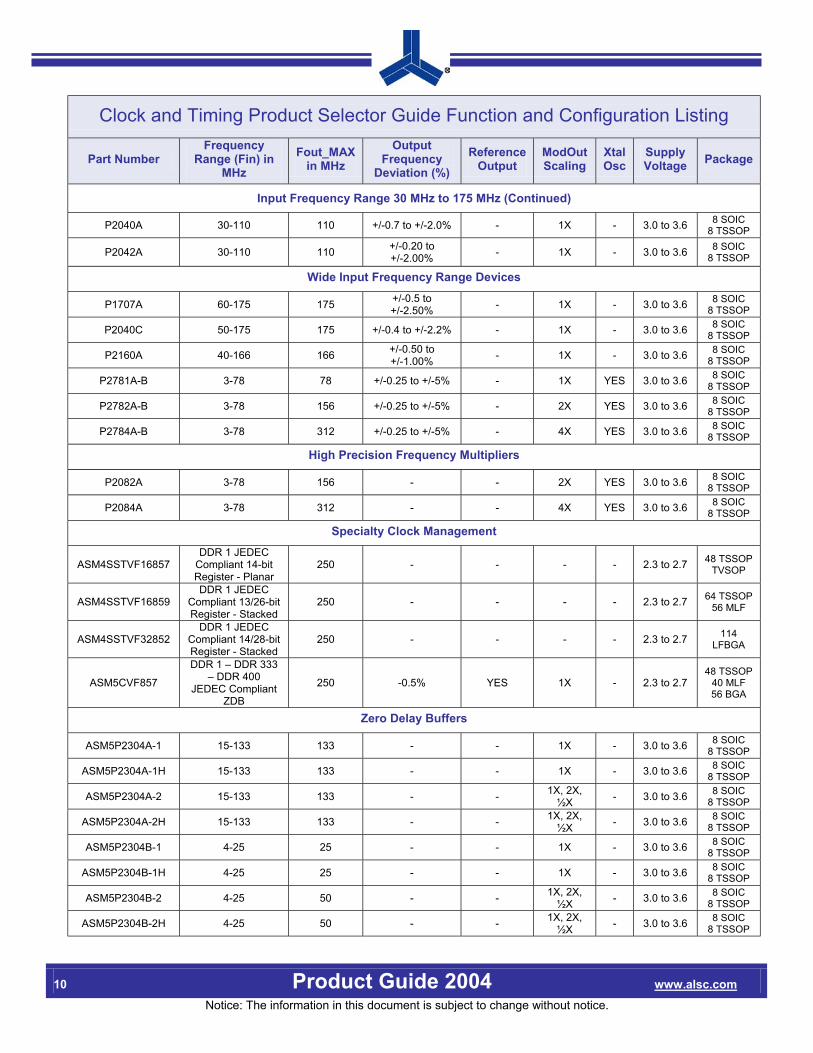
10 Product Guide 2004 www.alsc.com Notice: The information in this document is subject to change without notice.
Clock and Timing Product Selector Guide Function and Configuration Listing
Part Number Frequency
Range (Fin) in MHz
Fout_MAX in MHz
Output Frequency
Deviation (%) Reference
Output ModOut Scaling
Xtal Osc
Supply Voltage Package
Input Frequency Range 30 MHz to 175 MHz (Continued)
P2040A 30-110 110 +/-0.7 to +/-2.0% - 1X - 3.0 to 3.6 8 SOIC 8 TSSOP
P2042A 30-110 110 +/-0.20 to +/-2.00% - 1X - 3.0 to 3.6 8 SOIC
8 TSSOP
Wide Input Frequency Range Devices
P1707A 60-175 175 +/-0.5 to +/-2.50% - 1X - 3.0 to 3.6 8 SOIC
8 TSSOP
P2040C 50-175 175 +/-0.4 to +/-2.2% - 1X - 3.0 to 3.6 8 SOIC 8 TSSOP
P2160A 40-166 166 +/-0.50 to +/-1.00% - 1X - 3.0 to 3.6 8 SOIC
8 TSSOP
P2781A-B 3-78 78 +/-0.25 to +/-5% - 1X YES 3.0 to 3.6 8 SOIC 8 TSSOP
P2782A-B 3-78 156 +/-0.25 to +/-5% - 2X YES 3.0 to 3.6 8 SOIC 8 TSSOP
P2784A-B 3-78 312 +/-0.25 to +/-5% - 4X YES 3.0 to 3.6 8 SOIC 8 TSSOP
High Precision Frequency Multipliers
P2082A 3-78 156 - - 2X YES 3.0 to 3.6 8 SOIC 8 TSSOP
P2084A 3-78 312 - - 4X YES 3.0 to 3.6 8 SOIC 8 TSSOP
Specialty Clock Management
ASM4SSTVF16857 DDR 1 JEDEC
Compliant 14-bit Register - Planar
250 - - - - 2.3 to 2.7 48 TSSOP TVSOP
ASM4SSTVF16859 DDR 1 JEDEC
Compliant 13/26-bit Register - Stacked
250 - - - - 2.3 to 2.7 64 TSSOP 56 MLF
ASM4SSTVF32852 DDR 1 JEDEC
Compliant 14/28-bit Register - Stacked
250 - - - - 2.3 to 2.7 114 LFBGA
ASM5CVF857
DDR 1 – DDR 333 – DDR 400
JEDEC Compliant ZDB
250 -0.5% YES 1X - 2.3 to 2.7 48 TSSOP
40 MLF 56 BGA
Zero Delay Buffers
ASM5P2304A-1 15-133 133 - - 1X - 3.0 to 3.6 8 SOIC 8 TSSOP
ASM5P2304A-1H 15-133 133 - - 1X - 3.0 to 3.6 8 SOIC 8 TSSOP
ASM5P2304A-2 15-133 133 - - 1X, 2X, ½X - 3.0 to 3.6 8 SOIC
8 TSSOP
ASM5P2304A-2H 15-133 133 - - 1X, 2X, ½X - 3.0 to 3.6 8 SOIC
8 TSSOP
ASM5P2304B-1 4-25 25 - - 1X - 3.0 to 3.6 8 SOIC 8 TSSOP
ASM5P2304B-1H 4-25 25 - - 1X - 3.0 to 3.6 8 SOIC 8 TSSOP
ASM5P2304B-2 4-25 50 - - 1X, 2X, ½X - 3.0 to 3.6 8 SOIC
8 TSSOP
ASM5P2304B-2H 4-25 50 - - 1X, 2X, ½X - 3.0 to 3.6 8 SOIC
8 TSSOP

www.alsc.com Product Guide 2004 11 Notice: The information in this document is subject to change without notice.
Clock and Timing Product Selector Guide Function and Configuration Listing
Part Number Frequency
Range (Fin) in MHz
Fout_MAX in MHz
Output Frequency
Deviation (%) Reference
Output ModOut Scaling
Xtal Osc
Supply Voltage Package
ASM5P2305A-1 15-133 133 - - 1X - 3.0 to 3.6 8 SOIC 8 TSSOP
ASM5P2305A-1H 15-133 133 - - 1X - 3.0 to 3.6 8 SOIC 8 TSSOP
ASM5P2308A-1 15-133 133 - - 1X - 3.0 to 3.6 16 SOIC 16 TSSOP
ASM5P2308A-1H 15-133 133 - - 1X - 3.0 to 3.6 16 SOIC 16 TSSOP
ASM5P2308A-2 15-133 133 - - 1X, 2X, ½X - 3.0 to 3.6 16 SOIC
16 TSSOP
ASM5P2308A-3** 15-133 133 - - 2X, 4X - 3.0 to 3.6 16 SOIC TSSOP
ASM5P2308A-4 15-133 133 - - 2X, 2X - 3.0 to 3.6 16 SOIC 16 TSSOP
ASM5P2308A-5H 15-133 133 - - ½X, ½X - 3.0 to 3.6 16 SOIC 16 TSSOP
ASM5P2309A-1 15-133 133 - - 1X - 3.0 to 3.6 16 SOIC 16 TSSOP
ASM5P2309A-1H 15-133 133 - - 1X - 3.0 to 3.6 16 SOIC 16 TSSOP
ASM5P23S04A-1 15-133 133 - - 1X - 3.0 to 3.6 8 SOIC 8 TSSOP
ASM5P23S04A-1H 15-133 133 - - 1X - 3.0 to 3.6 8 SOIC 8 TSSOP
ASM5P23S04A-2 15-133 133 - - 1X, 2X, ½X - 3.0 to 3.6 8 SOIC
8 TSSOP
ASM5P23S04A-2H 15-133 133 - - 1X, 2X, ½X - 3.0 to 3.6 8 SOIC
8 TSSOP
ASM5P23S04A-5H 15-133 133 - - ½X, ½X - 3.0 to 3.6 8 SOIC 8 TSSOP
ASM5P23S05A-1 15-133 133 - - 1X - 3.0 to 3.6 8 SOIC 8 TSSOP
ASM5P23S05A-1H 15-133 133 - - 1X - 3.0 to 3.6 8 SOIC 8 TSSOP
ASM5P23S08A-1 15-133 133 - - 1X - 3.0 to 3.6 16 SOIC 16 TSSOP
ASM5P23S08A-1H 15-133 133 - - 1X - 3.0 to 3.6 16 SOIC 16 TSSOP
ASM5P23S08A-2 15-133 133 - - 1X, 2X, ½X - 3.0 to 3.6 16 SOIC
16 TSSOP
ASM5P23S08A-3** 15-133 133 - - 2X, 4X - 3.0 to 3.6 16 SOIC 16 TSSOP
ASM5P23S08A-4 15-133 133 - - 2X, 2X - 3.0 to 3.6 16 SOIC 16 TSSOP
ASM5P23S08A-5H 15-133 133 - - ½X, ½X - 3.0 to 3.6 16 SOIC 16 TSSOP
ASM5P23S09A-1 15-133 133 - - 1X - 3.0 to 3.6 16 SOIC 16 TSSOP
ASM5P23S09A-1H 15-133 133 - - 1X - 3.0 to 3.6 16 SOIC 16 TSSOP
** Output phase is indeterminant from INPUT REF. If needed in phase, use the –2 version.

12 Product Guide 2004 www.alsc.com Notice: The information in this document is subject to change without notice.
Zero Delay Buffers (ZDB) and Specialty Clock Management Cross Reference Guide
Alliance TI Cypress ICS IDT Pericom
ASM4SSTVF16857 SN74SSTVF16857 CY2SSTV16857 ICSSSTVF16857 IDT74SSTV16857 PI74SSTVF16857
ASM4SSTVF16859 SN74SSTVF16859 CY2SSTV16859 ICSSSTVF16859 IDT74SSTV16859 PI74SSTVF16859
ASM4SSTVF32582 SN74SSTVF32852 CY2SSTV32852 ICSSSTVF32852 IDT74SSTV32852 PI74SSTVF32852
ASM5PCVF857 CDCVF857 CY2SSTV857-32 ICS95V857 IDTCSPT857C PI6CVF857
ASM5P2304A-1 - CY2304-1 - - -
ASM5P2304A-2 - CY2304-2 - - -
ASM5P2304B-1 - CY2304-1 - - -
ASM5P2304B-2 - CY2304-2 - - -
ASM5P2305A-1 - CY2305-1 - IDT2305-1 PI6C2408-1
ASM5P2305A-1H - CY2305-H1 - IDT2305-1H PI6C2408-1H
ASM5P2308A-1 - CY2308-1 MK2308S-1 IDT2308-1 PI6C2408-1
ASM5P2308A-1H - CY2308-1H MK2308S-1H IDT2308-1H PI6C2408-1H
ASM5P2308A-2 - CY2308-2 - IDT2308-2 PI6C2408-2
ASM5P2308A-3 - CY2308-3 - IDT2308-3 PI6C2408-3
ASM5P2308A-4 - CY2308-4 - IDT2308-4 PI6C2408-4
ASM5P2308A-5H - CY2308-5H - IDT2308-5H -
ASM5P2309A-1 - CY2309 - IDT2309 -
ASM5P2309A-1H - CY2309-1H - IDT2309-1H -
ASM5P23S05A-1 - CY23S05 - IDT23S05 PI6C2405A-1
ASM5P23S05A-1H - CY23S05-1H - IDT23S05-1H PI6C2405A-1H
ASM5P23S08A-1 - CY23S08-1 - IDT23S08-1 PI6C2408-1
ASM5P23S08A-1H - CY230S8-1H - IDT23S08-1H PI6C2408-1H
ASM5P23S08A-2 - CY23S08-2 - IDT23S08-2 PI6C2408-2
ASM5P23S08A-3 - CY23S08-3 - IDT23S08-3 PI6C2408-3
ASM5P23S08A-4 - CY23S08-4 - IDT23S08-4 PI6C2408-4
ASM5P23S08A-5H - CY23S08-5H - IDT23S08-5H -
ASM5P23S09A-1H - CY23S09-1H - IDT23S09-1H PI62409-1H
ASM5P23S09A-1 - CY23S09-1 - IDT23S09 PI62409-1
Note: Alliance offers both SOIC & TSSOP, industrial or commercial temperature grades, and STD or lead-free package options for all devices listed.

www.alsc.com Product Guide 2004 13 Notice: The information in this document is subject to change without notice.
EMI Reduction Products Cross Reference Guide
Alliance Part Number
Input Frequency
(in MHz)
Frequency Selection Needed
Modulation Type
Cypress Part
Number
Output Frequency
(in MHz)
Frequency Selection Needed
Mobile Graphic
Frequency
AS80M2180 6-30 NO Down, Center W180/180i 8-28 4 ranges 27 MHz Source
ASM3P1819N 20-40 NO Down, Center CY25819 20-40 - 27 MHz Source
ASM3P2779A 20-38 NO Center - - - 27 MHz Source
ASM3P2811A 10-40 2 ranges Down, Center CY25811 10-40 3 ranges -
ASM3P2812A 10-40 2 ranges Down, Center CY25812 20-80 3 ranges -
ASM3P2814A 10-40 2 ranges Down, Center CY25814 40-160 3 ranges -
ASM3P2821B 15-27 NO Down CY25811 4-32 3 ranges -
ASM3P5821A 20-40 NO Down CY25811 4-32 3 ranges -
P1707A 60-175 NO Center SM561 54-166 10 ranges
LVDS Frequencies 65 MHz (XGA),
108 MHz (SXGA), and 162 MHz
(UXGA)
P1708C 50-110 NO Center SM560 25-108 10 ranges LVDS Frequencies
65 MHz (XGA), 108 MHz (SXGA)
P1819A-H 20-40 NO Down, Center CY25819 16-32 4 ranges 27 MHz Source
P2040C 60-175 NO Center - - -
LVDS Frequencies 65 MHz (XGA),
108 MHz (SXGA), and 162 MHz
(UXGA)
P2781A 3-78 4 ranges Center FS781 SOIC 6-82 4 ranges 25 MHz Source
P2781B 3-78 4 ranges Center FS781 TSSOP 6-82 4 ranges 27 MHz Source
P2782A 3-78 4 ranges Center FS782 SOIC 6-66 4 ranges -
P2782B 3-78 4 ranges Center FS782 TSSOP 6-66 4 ranges -
P2784A 3-78 4 ranges Center FS784 SOIC 6-32 4 ranges -
P2784B 3-78 4 ranges Center FS784 TSSOP 6-32 4 ranges -

14 Product Guide 2004 www.alsc.com Notice: The information in this document is subject to change without notice.
Power and Systems Management Products CPU Supervisor Products
Alliance Semiconductor provides cost effective, low power, Supervisor products that are an essential part of the 5V/3.3V/3V system providing active low and active high reset inputs to microprocessors, microcontrollers, ASICs, ASSPs, and digital systems. These Supervisor products initialize the systems into a known state and avoid malfunctioning of systems during power-up, power-down, power control, and brownout conditions, thus eliminating the possibility of code corruption. The CPU Supervisor Products also feature edge triggered and level triggered manual reset inputs. These enable the users to connect an external contact switch to generate a reset. This typically would be used as an alternative to operator intervention in systems that require reset. An early warning to the system controller about the impending system power failure, provided through the power fail input, enables the saving of essential system parameters. A Watch Dog Timer (WDT) is another useful feature that monitors and restarts a system processor. These are typically used as time out devices to force a system out of software “endless loop”. The reset outputs on the CPU Supervisor Products are available in Open Drain (OD) or Push Pull (PP) configurations to suit the user requirements. Various threshold voltage options are available on the supervisor devices, 4.63V, 4.38V, 4.00V, 3.08V, 2.93V, and 2.63V, which support 5%, 10%, and 20% system voltage tolerances. Reset timeout period options such as 140ms, 300 ms, and 800 ms cater to different system requirements. Dual power supply monitoring is a highly useful feature that is essential in the design of one core supply and IO supply systems. This system architecture is gaining wide acceptance. The CPU and System Supervisor Products are available in industry standard, space saving packages such as SOT-23, SOT-143, SO-8, and Micro SO in commercial and industrial temperature range. Supervisor devices are found in computers, embedded systems, portable and battery operated systems, notebook PCs, cellular phones, safety systems, automotive systems, wireless communication systems, PDAs, printers, set top boxes, intelligent systems and others.

www.alsc.com Product Guide 2004 15 Notice: The information in this document is subject to change without notice.
CPU Supervisor Product Selector Guide Specifications Features
RST Output Stage
Alliance Part Number Input Voltage (V) Min to Max Vth (V) Temp PFD WDT
Batt Back
up L H MR
OD PP
Package
CPU Supervisors with Selectable Trip-point Tolerance, Watchdog timer with POR
ASM1232LP 4.5-5.5 Vt1 T1 - X - X X L X X 8P-DIP
ASM1232LPCMA 4.5-5.5 Vt1 T1 - X - X X L X X 8-MicroSO
ASM1232LPEMA 4.5-5.5 Vt1 T2 - X - X X L X X 8-MicroSO
ASM1232LPN 4.5-5.5 Vt1 T2 - X - X X L X X 8P-DIP
ASM1232LPS 4.5-5.5 Vt1 T1 - X - X X L X X 16-SO
ASM1232LPS-2 4.5-5.5 Vt1 T1 - X - X X L X X 8-SO
ASM1232LPSN 4.5-5.5 Vt1 T2 - X - X X L X X 16-SO
ASM1232LPSN-2 4.5-5.5 Vt1 T2 - X - X X L X X 8-SO
ASM1832 1.0-5.5 Vt1 T2 - X - X X L - X 8P-DIP
ASM1832EMA 1.0-5.5 Vt1 T2 - X - X X L - X 8-MicroSO
ASM1832S 1.0-5.5 Vt1 T2 - X - X X L - X 8-SO
CPU Supervisors with POR, Edge Triggered MR
ASM161JEUS 1.1-5.5 4 T2 - - - X - ↓ X - 4L-SOT143
ASM161LEUS 1.1-5.5 4.63 T2 - - - X - ↓ X - 4L-SOT143
ASM161MEUS 1.1-5.5 4.38 T2 - - - X - ↓ X - 4L-SOT143
ASM161REUS 1.1-5.5 2.63 T2 - - - X - ↓ X - 4L-SOT143
ASM161SEUS 1.1-5.5 2.93 T2 - - - X - ↓ X - 4L-SOT143
ASM161TEUS 1.1-5.5 3.08 T2 - - - X - ↓ X - 4L-SOT143
ASM162JEUS 1.1-5.5 4 T2 - - - - - ↓ - X 4L-SOT143
ASM162LEUS 1.1-5.5 4.63 T2 - - - - - ↓ - X 4L-SOT143
ASM162MEUS 1.1-5.5 4.38 T2 - - - - - ↓ - X 4L-SOT143
ASM162REUS 1.1-5.5 2.63 T2 - - - - - ↓ - X 4L-SOT143
ASM162SEUS 1.1-5.5 2.93 T2 - - - - - ↓ - X 4L-SOT143
ASM162TEUS 1.1-5.5 3.08 T2 - - - - - ↓ - X 4L-SOT143
Legend: Vth = Threshold, PFD = Power Fail Detect, WDT = Watch Dog Timer, RST = Reset, MR = Manual Reset, OD = Open Drain, PP = Push Pull, T1 = 0°C to +70°C, T2 = -40°C to + 85°C, T3 = -40°C to +105°C, H = High, L = Low, ↓ = Edge Triggered, Vt1 = Selectable between 4.62V or 4.37V, Vt2 = Selectable between 4.63V or 4.38V, and 2.88V or 2.55V.

16 Product Guide 2004 www.alsc.com Notice: The information in this document is subject to change without notice.
CPU Supervisor Product Selector Guide Specifications Features
RST Output Stage
Alliance Part Number Input Voltage (V) Min to Max Vth (V) Temp PFD WDT
Batt Back
up L H MR
OD PP
Package
Low Power CPU Supervisors
ASM1233DZ-10 1.2-5.5 4.375 T2 - - - X - - X - 4L-SOT223
ASM1233AZ-15 1.2-5.5 2.72 T2 - - - X - - X - 4L-SOT223
ASM1233DZ-15 1.2-5.5 4.125 T2 - - - X - - X - 4L-SOT223
ASM1233DZ-5 1.2-5.5 4.625 T2 - - - X - - X - 4L-SOT223
ASM1233MS-3 1.2-5.5 2.72 T2 - - - X - - X - 8-SO
ASM1233MS-5 1.2-5.5 4.375 T2 - - - X - - X - 8-SO
ASM1233MS-55 1.2-5.5 4.625 T2 - - - X - - X - 8-SO
ASM1810R-10 1.2-5.5 4.37 T2 - - - X - - - X 3L-SOT23
ASM1810R-15 1.2-5.5 4.12 T2 - - - X - - - X 3L-SOT23
ASM1810R-5 1.2-5.5 4.62 T2 - - - X - - - X 3L-SOT23
ASM1811R-10 1.2-5.5 4.35 T2 - - - X - - X - 3L-SOT23
ASM1811R-15 1.2-5.5 4.13 T2 - - - X - - X - 3L-SOT23
ASM1811R-5 1.2-5.5 4.62 T2 - - - X - - X - 3L-SOT23
ASM1812R-10 1.2-5.5 4.35 T2 - - - - X - - X 3L-SOT23
ASM1812R-15 1.2-5.5 4.13 T2 - - - - X - - X 3L-SOT23
ASM1812R-5 1.2-5.5 4.62 T2 - - - - X - - X 3L-SOT23
ASM1815R-10 1.2-5.5 2.88 T2 - - - X - - - X 3L-SOT23
ASM1815R-20 1.2-5.5 2.55 T2 - - - X - - - X 3L-SOT23
ASM1815R-5 1.2-5.5 3.06 T2 - - - X - - - X 3L-SOT23
ASM1816R-10 1.2-5.5 2.88 T2 - - - X - - X - 3L-SOT23
ASM1816R-20 1.2-5.5 2.55 T2 - - - X - - X - 3L-SOT23
ASM1816R-5 1.2-5.5 3.06 T2 - - - X - - X - 3L-SOT23
ASM1817R-10 1.2-5.5 2.88 T2 - - - - X - - X 3L-SOT23
ASM1817R-20 1.2-5.5 2.55 T2 - - - - X - - X 3L-SOT23
Legend: Vth = Threshold, PFD = Power Fail Detect, WDT = Watch Dog Timer, RST = Reset, MR = Manual Reset, OD = Open Drain, PP = Push Pull, T1 = 0°C to +70°C, T2 = -40°C to + 85°C, T3 = -40°C to +105°C, H = High, L = Low, ↓ = Edge Triggered, Vt1 = Selectable between 4.62V or 4.37V, Vt2 = Selectable between 4.63V or 4.38V, and 2.88V or 2.55V.

www.alsc.com Product Guide 2004 17 Notice: The information in this document is subject to change without notice.
CPU Supervisor Product Selector Guide Specifications Features
RST Output Stage
Alliance Part Number Input Voltage (V) Min to Max Vth (V) Temp PFD WDT
Batt Back
up L H MR
OD PP
Package
ASM1817R-5 1.2-5.5 3.06 T2 - - - - X - - X 3L-SOT23
ASM8500-27 1.0-5.5 2.7 T2 - - - X - - X - 3L-SOT89
ASM8500-29 1.0-5.5 2.93 T2 - - - X - - X - 3L-SOT89
ASM8500-42 1.0-5.5 4.2 T2 - - - X - - X - 3L-SOT89
CPU Supervisors with Dual Supply Monitoring, Selectable Threshold
ASM1834 1.2-5.5 Vt2 T2 - - - X - L - X 8P-DIP
ASM1834A 1.2-5.5 Vt2 T2 - - - X - L X X 8P-DIP
ASM1834AEMA 1.2-5.5 Vt2 T2 - - - X - L X X 8-MicroSO
ASM1834AS 1.2-5.5 Vt2 T2 - - - X - L X X 8-SO
ASM1834D 1.2-5.5 Vt2 T2 - - - - X L X X 8P-DIP
ASM1834DEMA 1.2-5.5 Vt2 T2 - - - - X L - X 8-MicroSO ASM1834DS 1.2-5.5 Vt2 T2 - - - - X L - X 8-SO
ASM1834EMA 1.2-5.5 Vt2 T2 - - - X - L - X 8-MicroSO ASM1834S 1.2-5.5 Vt2 T2 - - - X - L - X 8-SO
CPU Supervisors with Watchdog Timer, Battery Backup, and Power Fail Detector
ASM690ACPA 1.1-5.5 4.65 T1 X X X X - - - X 8P-DIP ASM690ACSA 1.1-5.5 4.65 T1 X X X X - - - X 8-SO ASM690AEPA 1.1-5.5 4.65 T2 X X X X - - - X 8P-DIP ASM690AESA 1.1-5.5 4.65 T2 X X X X - - - X 8-SO ASM692ACPA 1.1-5.5 4.4 T1 X X X X - - - X 8P-DIP ASM692ACSA 1.1-5.5 4.4 T1 X X X X - - - X 8-SO ASM692AEPA 1.1-5.5 4.4 T2 X X X X - - - X 8P-DIP ASM692AESA 1.1-5.5 4.4 T2 X X X X - - - X 8-SO
ASM802LCPA 1.1-5.5 4.65 T1 X X X X - - - X 8P-DIP
ASM802LCSA 1.1-5.5 4.65 T1 X X X X - - - X 8-SO
ASM802LEPA 1.1-5.5 4.65 T2 X X X X - - - X 8P-DIP
ASM802LESA 1.1-5.5 4.65 T2 X X X X - - - X 8-SO
ASM802MCPA 1.1-5.5 4.4 T1 X X X X - - - X 8P-DIP
ASM802MCSA 1.1-5.5 4.4 T1 X X X X - - - X 8-SO
ASM802MEPA 1.1-5.5 4.4 T2 X X X X - - - X 8P-DIP
Legend: Vth = Threshold, PFD = Power Fail Detect, WDT = Watch Dog Timer, RST = Reset, MR = Manual Reset, OD = Open Drain, PP = Push Pull, T1 = 0°C to +70°C, T2 = -40°C to + 85°C, T3 = -40°C to +105°C, H = High, L = Low, ↓ = Edge Triggered, Vt1 = Selectable between 4.62V or 4.37V, Vt2 = Selectable between 4.63V or 4.38V, and 2.88V or 2.55V.

18 Product Guide 2004 www.alsc.com Notice: The information in this document is subject to change without notice.
CPU Supervisor Product Selector Guide Specifications Features
RST Output Stage
Alliance Part Number Input Voltage (V) Min to Max Vth (V) Temp PFD WDT
Batt Back
up L H MR
OD PP
Package
ASM802MESA 1.1-5.5 4.4 T2 X X X X - - - X 8-SO
ASM805LCPA 1.1-5.5 4.65 T1 X X X - X - - X 8P-DIP
ASM805LCSA 1.1-5.5 4.65 T1 X X X - X - - X 8-SO
ASM805LEPA 1.1-5.5 4.65 T2 X X X - X - - X 8P-DIP
ASM805LESA 1.1-5.5 4.65 T2 X X X - X - - X 8-SO
CPU Supervisors with Watchdog Timer and Power Fail Detector
ASM705CPA 1.2-5.5 4.65 T1 X X - X - L - X 8P-DIP
ASM705CSA 1.2-5.5 4.65 T1 X X - X - L - X 8-SO
ASM705CUA 1.2-5.5 4.65 T1 X X - X - L - X 8-MicroSO
ASM705EPA 1.2-5.5 4.65 T2 X X - X - L - X 8P-DIP
ASM705ESA 1.2-5.5 4.65 T2 X X - X - L - X 8-SO
ASM706CPA 1.2-5.5 4.4 T1 X X - X - L - X 8P-DIP
ASM706CSA 1.2-5.5 4.4 T1 X X - X - L - X 8-SO
ASM706CUA 1.2-5.5 4.4 T1 X X - X - L - X 8-MicroSO
ASM706EPA 1.2-5.5 4.4 T2 X X - X - L - X 8P-DIP
ASM706ESA 1.2-5.5 4.4 T2 X X - X - L - X 8-SO
ASM706JCPA 1.1-5.5 4 T1 X X - X - L - X 8P-DIP
ASM706JCSA 1.1-5.5 4 T1 X X - X - L - X 8-SO
ASM706JCUA 1.1-5.5 4 T1 X X - X - L - X 8-MicroSO
ASM706JEPA 1.2-5.5 4 T2 X X - X L - X 8P-DIP
ASM706JESA 1.2-5.5 4 T2 X X - X - L - X 8-SO
ASM706PCPA 1.1-5.5 2.63 T1 X X - X L - X 8P-DIP
ASM706PCSA 1.1-5.5 2.63 T1 X X - X L - X 8-SO
ASM706PCUA 1.1-5.5 2.63 T1 X X - X L - X 8-MicroSO
ASM706PEPA 1.2-5.5 2.63 T2 X X - X L - X 8P-DIP
ASM706PESA 1.2-5.5 2.63 T2 X X - X L - X 8-SO
ASM706RCPA 1.1-5.5 2.63 T1 X X - X - L - X 8P-DIP
ASM706RCSA 1.1-5.5 2.63 T1 X X - X - L - X 8-SO
ASM706RCUA 1.1-5.5 2.63 T1 X X - X - L - X 8-MicroSO
Legend: Vth = Threshold, PFD = Power Fail Detect, WDT = Watch Dog Timer, RST = Reset, MR = Manual Reset, OD = Open Drain, PP = Push Pull, T1 = 0°C to +70°C, T2 = -40°C to + 85°C, T3 = -40°C to +105°C, H = High, L = Low, ↓ = Edge Triggered, Vt1 = Selectable between 4.62V or 4.37V, Vt2 = Selectable between 4.63V or 4.38V, and 2.88V or 2.55V.

www.alsc.com Product Guide 2004 19 Notice: The information in this document is subject to change without notice.
CPU Supervisor Product Selector Guide Specifications Features
RST Output Stage
Alliance Part Number Input Voltage (V) Min to Max Vth (V) Temp PFD WDT
Batt Back
up L H MR
OD PP
Package
ASM706REPA 1.2-5.5 2.63 T2 X X - X - L - X 8P-DIP
ASM706RESA 1.2-5.5 2.63 T2 X X - X - L - X 8-SO
ASM706SCPA 1.1-5.5 2.93 T1 X X - X - L - X 8P-DIP
ASM706SCSA 1.1-5.5 2.93 T1 X X - X - L - X 8-SO
ASM706SCUA 1.1-5.5 2.93 T1 X X - X - L - X 8-MicroSO
ASM706SEPA 1.2-5.5 2.93 T2 X X - X - L - X 8P-DIP
ASM706SESA 1.2-5.5 2.93 T2 X X - X - L - X 8-SO
ASM706TCPA 1.1-5.5 3.08 T1 X X - X - L - X 8P-DIP
ASM706TCSA 1.1-5.5 3.08 T1 X X - X - L - X 8-SO
ASM706TCUA 1.1-5.5 3.08 T1 X X - X - L - X 8-MicroSO
ASM706TEPA 1.2-5.5 3.08 T2 X X - X - L - X 8P-DIP
ASM706TESA 1.2-5.5 3.08 T2 X X - X - L - X 8-SO
ASM813LCPA 1.1-5.5 4.65 T1 X X - - X L - X 8P-DIP
ASM813LCSA 1.1-5.5 4.65 T1 X X - - X L - X 8-SO
ASM813LCUA 1.1-5.5 4.65 T1 X X - - X L - X 8-MicroSO
ASM813LEPA 1.1-5.5 4.65 T2 X X - - X L - X 8P-DIP
ASM813LESA 1.1-5.5 4.65 T2 X X - - X L - X 8-SO
CPU Supervisors with Power Fail Detector
ASM707CPA 1.2-5.5 4.65 T1 X - - X X L - X 8P-DIP
ASM707CSA 1.2-5.5 4.65 T1 X - - X X L - X 8-SO
ASM707CUA 1.2-5.5 4.65 T1 X - - X X L - X 8-MicroSO
ASM707EPA 1.2-5.5 4.65 T2 X - - X X L - X 8P-DIP
ASM707ESA 1.2-5.5 4.65 T2 X - - X X L - X 8-SO
ASM708CPA 1.2-5.5 4.4 T1 X - - X X L - X 8P-DIP
ASM708CSA 1.2-5.5 4.4 T1 X - - X X L - X 8-SO
ASM708CUA 1.2-5.5 4.4 T1 X - - X X L - X 8-MicroSO
ASM708EPA 1.2-5.5 4.4 T2 X - - X X L - X 8P-DIP
ASM708ESA 1.2-5.5 4.4 T2 X - - X X L - X 8-SO
ASM708JCPA 1.1-5.5 4 T1 X - - X X L - X 8P-DIP
ASM708JCSA 1.1-5.5 4 T1 X - - X X L - X 8-SO
ASM708JCUA 1.1-5.5 4 T1 X - - X X L - X 8-MicroSO
ASM708JEPA 1.2-5.5 4 T2 X - - X X L - X 8P-DIP
ASM708JESA 1.2-5.5 4 T2 X - - X X L - X 8-SO
Legend: Vth = Threshold, PFD = Power Fail Detect, WDT = Watch Dog Timer, RST = Reset, MR = Manual Reset, OD = Open Drain, PP = Push Pull, T1 = 0°C to +70°C, T2 = -40°C to + 85°C, T3 = -40°C to +105°C, H = High, L = Low, ↓ = Edge Triggered, Vt1 = Selectable between 4.62V or 4.37V, Vt2 = Selectable between 4.63V or 4.38V, and 2.88V or 2.55V.

20 Product Guide 2004 www.alsc.com Notice: The information in this document is subject to change without notice.
CPU Supervisor Product Selector Guide Specifications Features
RST Output Stage
Alliance Part Number Input Voltage (V) Min to Max Vth (V) Temp PFD WDT
Batt Back
up L H MR
OD PP
Package
ASM708RCPA 1.1-5.5 2.63 T1 X - - X X L - X 8P-DIP
ASM708RCSA 1.1-5.5 2.63 T1 X - - X X L - X 8-SO
ASM708RCUA 1.1-5.5 2.63 T1 X - - X X L - X 8-MicroSO
ASM708REPA 1.2-5.5 2.63 T2 X - - X X L - X 8P-DIP
ASM708RESA 1.2-5.5 2.63 T2 X - - X X L - X 8-SO
ASM708SCPA 1.1-5.5 2.93 T1 X - - X X L - X 8P-DIP
ASM708SCSA 1.1-5.5 2.93 T1 X - - X X L - X 8-SO
ASM708SCUA 1.1-5.5 2.93 T1 X - - X X L - X 8-MicroSO
ASM708SEPA 1.2-5.5 2.93 T2 X - - X X L - X 8P-DIP
ASM708SESA 1.2-5.5 2.93 T2 X - - X X L - X 8-SO
ASM708TCPA 1.1-5.5 3.08 T1 X - - X X L - X 8P-DIP
ASM708TCSA 1.1-5.5 3.08 T1 X - - X X L - X 8-SO
ASM708TCUA 1.1-5.5 3.08 T1 X - - X X L - X 8-MicroSO
ASM708TEPA 1.2-5.5 3.08 T2 X - - X X L - X 8P-DIP
ASM708TESA 1.2-5.5 3.08 T2 X - - X X L - X 8-SO
Low Power CPU Supervisors
ASM809JEUR 1.2-5.5 4 T3 - - - X - - - X 3L-SOT23
ASM809LEUR 1.2-5.5 4.63 T3 - - - X - - - X 3L-SOT23
ASM809MEUR 1.2-5.5 4.38 T3 - - - X - - - X 3L-SOT23
ASM809REUR 1.2-5.5 2.63 T3 - - - X - - - X 3L-SOT23
ASM809SEUR 1.2-5.5 2.93 T3 - - - X - - - X 3L-SOT23
ASM809TEUR 1.2-5.5 3.08 T3 - - - X - - - X 3L-SOT23
ASM810JEUR 1.2-5.5 4 T3 - - - - X - - X 3L-SOT23
ASM810LEUR 1.2-5.5 4.63 T3 - - - - X - - X 3L-SOT23
ASM810MEUR 1.2-5.5 4.38 T3 - - - - X - - X 3L-SOT23
ASM810REUR 1.2-5.5 2.63 T3 - - - - X - - X 3L-SOT23
ASM810SEUR 1.2-5.5 2.93 T3 - - - - X - - X 3L-SOT23
ASM810TEUR 1.2-5.5 3.08 T3 - - - - X - - X 3L-SOT23
Legend: Vth = Threshold, PFD = Power Fail Detect, WDT = Watch Dog Timer, RST = Reset, MR = Manual Reset, OD = Open Drain, PP = Push Pull, T1 = 0°C to +70°C, T2 = -40°C to + 85°C, T3 = -40°C to +105°C, H = High, L = Low, ↓ = Edge Triggered, Vt1 = Selectable between 4.62V or 4.37V, Vt2 = Selectable between 4.63V or 4.38V, and 2.88V or 2.55V.

www.alsc.com Product Guide 2004 21 Notice: The information in this document is subject to change without notice.
CPU Supervisor Product Selector Guide Specifications Features
RST Output Stage
Alliance Part Number Input Voltage (V) Min to Max Vth (V) Temp PFD WDT
Batt Back
up L H MR
OD PP
Package
ASM811JEUS 1.2-5.5 4 T3 - - - X - L - X 4L-SOT143
ASM811LEUS 1.2-5.5 4.63 T3 - - - X - L - X 4L-SOT143
ASM811MEUS 1.2-5.5 4.38 T3 - - - X - L - X 4L-SOT143
ASM811REUS 1.2-5.5 2.63 T3 - - - X - L - X 4L-SOT143
ASM811SEUS 1.2-5.5 2.93 T3 - - - X - L - X 4L-SOT143
ASM811TEUS 1.2-5.5 3.08 T3 - - - X - L - X 4L-SOT143
ASM812JEUS 1.2-5.5 4 T3 - - - - X L - X 4L-SOT143
ASM812LEUS 1.2-5.5 4.63 T3 - - - - X L - X 4L-SOT143
ASM812MEUS 1.2-5.5 4.38 T3 - - - - X L - X 4L-SOT143
ASM812REUS 1.2-5.5 2.63 T3 - - - - X L - X 4L-SOT143
ASM812SEUS 1.2-5.5 2.93 T3 - - - - X L - X 4L-SOT143
ASM812TEUS 1.2-5.5 3.08 T3 - - - - X L - X 4L-SOT143
Legend: Vth = Threshold, PFD = Power Fail Detect, WDT = Watch Dog Timer, RST = Reset, MR = Manual Reset, OD = Open Drain, PP = Push Pull, T1 = 0°C to +70°C, T2 = -40°C to + 85°C, T3 = -40°C to +105°C, H = High, L = Low, ↓ = Edge Triggered, Vt1 = Selectable between 4.62V or 4.37V, Vt2 = Selectable between 4.63V or 4.38V, and 2.88V or 2.55V. All products in SOT-23 and SOT-143 package are only offered in Tape and Reel.To order parts in Tape and Reel,add “-T” to part number.

22 Product Guide 2004 www.alsc.com Notice: The information in this document is subject to change without notice.
CPU Supervisor Cross Reference Guide
Alliance Maxim/Dallas IMP Analog Devices Micrel Microchip
ASM1232LP DS1232LPS-2 IMP1232LP MIC1232N TC1232CPA
ASM1232LPCMA DS1232LPµ IMP1232LPCMA - - -
ASM1232LPEMA DS1232LPµ IMP1232LPEMA - - -
ASM1232LPN DS1232LP IMP1232LPN - MIC1232N TC1232EPA
ASM1232LPS DS1232LPS IMP1232LPS - - TC1232COE
ASM1232LPS-2 DS1232LPSN-2 IMP1232LPS-2 - MIC1232M TC1232COA
ASM1232LPSN DS1232LPS IMP1232LPSN - - TC1232EOE
ASM1232LPSN-2 DS1232LPSN-2 IMP1232LPSN-2 - MIC1232M TC1232EOA
ASM1233AZ-15 DS1233A-15 - - - -
ASM1233DZ-5 DS1233DZ-5 IMP1233DZ-5 - - -
ASM1233DZ-10 DS1233DZ-10 IMP1233DZ-10 - - -
ASM1233DZ-15 DS1233DZ-15 IMP1233DZ-15 - - -
ASM1233MS-55 DS1233MS-55 IMP1233MS-55 - - -
ASM1233MS-5 DS1233MS-5 IMP1233MS-5 - - -
ASM1233MS-3 DS1233MS-3 IMP1233MS-3 - - -
ASM161JEUS MAX6467US40 IMP161JEUS - - -
ASM161LEUS MAX6467US46 IMP161LEUS - - -
ASM161MEUS MAX6467US44 IMP161MEUS - - -
ASM161REUS MAX6467US26 IMP161REUS - - -
ASM161SEUS MAX6467US29 IMP161SEUS - - -
ASM161TEUS MAX6467US31 IMP161TEUS - - -
ASM162JEUS - IMP162JEUS - - -
ASM162LEUS - IMP162LEUS - - -
ASM162MEUS - IMP162MEUS - - -
ASM162REUS - IMP162REUS - - -
ASM162SEUS - IMP162SEUS - - -
ASM162TEUS - IMP162TEUS - - -
ASM1810R-5 DS1810R-5 IMP1810R-5 - MIC1810-5U TC1272-5
ASM1810R-10 DS1810R-10 IMP1810R-10 - MIC1810-10U TC1272-10
ASM1810R-15 DS1810R-15 IMP1810R-15 - MIC1810-15U TC1272-15
ASM1811R-5 DS1811R-5 IMP1811R-5 - - -
ASM1811R-10 DS1811R-10 IMP1811R-10 - - -
ASM1811R-15 DS1811R-15 IMP1811R-15 - - -
ASM1812R-5 DS1812R-5 IMP1812R-5 - - TC1274-5
ASM1812R-10 DS1812R-10 IMP1812R-10 - - TC1274-10
ASM1812R-15 DS1812R-15 IMP1812R-15 - - TC1274-15
ASM1815R-5 DS1815R-5 IMP1815R-5 - MIC1815-5U TC1275-5
ASM1815R-10 DS1815R-10 IMP1815R-10 - MIC1815-10U TC1275-10
ASM1815R-20 DS1815R-20 IMP1815R-20 - MIC1815-20U TC1275-20
ASM1816R-5 DS1816R-5 IMP1816R-5 - - TC1276-5
ASM1816R-10 DS1816R-10 IMP1816R-10 - - TC1276-10
ASM1816R-20 DS1816R-20 IMP1816R-20 - - TC1276-20

www.alsc.com Product Guide 2004 23 Notice: The information in this document is subject to change without notice.
CPU Supervisor Cross Reference Guide
Alliance Maxim/Dallas IMP Analog Devices Micrel Microchip
ASM1817R-5 DS1817R-5 IMP1817R-5 - - TC1277-5
ASM1817R-10 DS1817R-10 IMP1817R-10 - - TC1277-10
ASM1817R-20 DS1817R-20 IMP1817R-20 - - TC1277-20
ASM1832 DS1832 IMP1832 - MIC1832N -
ASM1832EMA DS1832UN IMP1832EMA - - -
ASM1832S DS1832S IMP1832S - MIC1832M -
ASM1834 DS1834 IMP1834 - - -
ASM1834A DS1834CMA IMP1834A - - -
ASM1834AEMA DS1834AU IMP1834AEMA - - -
ASM1834AS DS1834ASM IMP1834AS - - -
ASM1834D DS1834D IMP1834D - - -
ASM1834DEMA DS1834DU IMP1834DEMA - - -
ASM1834DS DS1834DS IMP1834DS - - -
ASM1834EMA DS1834U IMP1834EMA - - -
ASM1834S DS1834S IMP1834S - - -
ASM690ACPA MAX690ACPA IMP690ACPA ADM690AAN - -
ASM690ACSA MAX690ACSA IMP690ACSA ADM690AARN - -
ASM690AEPA MAX690AEPA IMP690AEPA ADM690AAN - -
ASM690AESA MAX690AESA IMP690AESA ADM690AARN - -
ASM692ACPA MAX692ACPA IMP692ACPA ADM692AAN - -
ASM692ACSA MAX692ACSA IMP692ACSA ADM692AARN - -
ASM692AEPA MAX692AEPA IMP692AEPA ADM692AAN - -
ASM692AESA MAX692AESA IMP692AESA ADM692AARN - -
ASM705CPA MAX705CPA IMP705CPA ADM705AN MIC705N -
ASM705CSA MAX705CSA IMP705CSA ADM705AR MIC705M -
ASM705CUA MAX705CUA IMP705CUA - - -
ASM705EPA MAX705EPA IMP705EPA ADM705AN MIC705N -
ASM705ESA MAX705ESA IMP705ESA ADM705AR MIC705M -
ASM706CPA MAX706CPA IMP706CPA ADM706AN MIC706N -
ASM706CSA MAX706CSA IMP706CSA ADM706AR MIC706M -
ASM706CUA MAX706CUA IMP706CUA - - -
ASM706EPA MAX706EPA IMP706EPA ADM706AN MIC706N -
ASM706ESA MAX706ESA IMP706ESA ADM706AR MIC706M -
ASM706JCPA MAX706JCPA IMP706JCPA - - -
ASM706JCSA MAX706JCSA IMP706JCSA - - -
ASM706JCUA MAX706JCUA IMP706JCUA - - -
ASM706JEPA MAX706JEPA IMP706JEPA - - -
ASM706JESA MAX706JESA IMP706JESA - - -
ASM706PCPA MAX706PCPA IMP706PCPA ADM706PAN MIC706PN -
ASM706PCSA MAX706PCSA IMP706PCSA ADM706PAR MIC706PM -
ASM706PCUA MAX706PCUA IMP706PCUA - - -
ASM706PEPA MAX706PEPA IMP706PEPA ADM706PAN MIC706PN -
ASM706PESA MAX706PESA IMP706PESA ADM706PAR MIC706PM -

24 Product Guide 2004 www.alsc.com Notice: The information in this document is subject to change without notice.
CPU Supervisor Cross Reference Guide
Alliance Maxim/Dallas IMP Analog Devices Micrel Microchip
ASM706RCPA MAX706RCPA IMP706RCPA ADM706RAN MIC706RN -
ASM706RCSA MAX706RCSA IMP706RCSA ADM706RAR MIC706RM -
ASM706RCUA MAX706RCUA IMP706RCUA - - -
ASM706REPA MAX706REPA IMP706REPA ADM706RAN MIC706RN -
ASM706RESA MAX706RESA IMP706RESA ADM706RAR MIC706RM -
ASM706SCPA MAX706SCPA IMP706SCPA ADM706SAN MIC706SN -
ASM706SCSA MAX706SCSA IMP706SCSA ADM706SAR MIC706SM -
ASM706SCUA MAX706SCUA IMP706SCUA - - -
ASM706SEPA MAX706SEPA IMP706SEPA ADM706SAN MIC706SN -
ASM706SESA MAX706SESA IMP706SESA ADM706SAR MIC706SM -
ASM706TCPA MAX706TCPA IMP706TCPA ADM706TAN MIC706TN -
ASM706TCSA MAX706TCSA IMP706TCSA ADM706TAR MIC706TM -
ASM706TCUA MAX706TCUA IMP706TCUA - - -
ASM706TEPA MAX706TEPA IMP706TEPA ADM706TAN MIC706TN -
ASM706TESA MAX706TESA IMP706TESA ADM706TAR MIC706TM -
ASM707CPA MAX707CPA IMP707CPA ADM707AN MIC707N -
ASM707CSA MAX707CSA IMP707CSA ADM707AR MIC707M -
ASM707CUA MAX707CUA IMP707CUA ADM707ARM - -
ASM707EPA MAX707EPA IMP707EPA ADM707AN MIC707N -
ASM707ESA MAX707ESA IMP707ESA ADM707AR MIC707M -
ASM708CPA MAX708CPA IMP708CPA ADM708AN MIC708N -
ASM708CSA MAX708CSA IMP708CSA ADM708AR MIC708M -
ASM708CUA MAX708CUA IMP708CUA ADM708ARM - -
ASM708EPA MAX708EPA IMP708EPA ADM708AN MIC708N -
ASM708ESA MAX708ESA IMP708ESA ADM708AR MIC708M -
ASM708JCPA - IMP708JCPA - - -
ASM708JCSA - IMP708JCSA - - -
ASM708JCUA - IMP708JCUA - - -
ASM708JEPA - IMP708JEPA - - -
ASM708JESA - IMP708JESA - - -
ASM708RCPA MAX708RCPA IMP708RCPA ADM708RAN MIC708RN -
ASM708RCSA MAX708RCSA IMP708RCSA ADM708RAR MIC708RM -
ASM708RCUA MAX708RCUA IMP708RCUA - - -
ASM708REPA MAX708REPA IMP708REPA ADM708RAN MIC708RN -
ASM708RESA MAX708RESA IMP708RESA ADM708RAR MIC708RM -
ASM708SCPA MAX708SCPA IMP708SCPA ADM708SAN MIC708SN -
ASM708SCSA MAX708SCSA IMP708SCSA ADM708SAR MIC708SM -
ASM708SCUA MAX708SCUA IMP708SCUA - - -
ASM708SEPA MAX708SEPA IMP708SEPA ADM708SAN MIC708SN -
ASM708SESA MAX708SESA IMP708SESA ADM708SAR MIC708SM -
ASM708TCPA MAX708TCPA IMP708TCPA ADM708TAN MIC708TN -
ASM708TCSA MAX708TCSA IMP708TCSA ADM708TAR MIC708TM -
ASM708TCUA MAX708TCUA IMP708TCUA - - -

www.alsc.com Product Guide 2004 25 Notice: The information in this document is subject to change without notice.
CPU Supervisor Cross Reference Guide
Alliance Maxim/Dallas IMP Analog Devices Micrel Microchip
ASM708TEPA MAX708TEPA IMP708TEPA ADM708TAN MIC708TN -
ASM708TESA MAX708TESA IMP708TESA ADM708TAR MIC708TM -
ASM802LCPA MAX802LCPA IMP802LCPA ADM802LAN - -
ASM802LCSA MAX802LCSA IMP802LCSA ADM802LARN - -
ASM802LEPA MAX802LEPA IMP802LEPA ADM802LAN - -
ASM802LESA MAX802LESA IMP802LESA ADM802LARN - -
ASM802MCPA MAX802MCPA IMP802MCPA ADM802MAN - -
ASM802MCSA MAX802MCSA IMP802MCSA ADM802MARN - -
ASM802MEPA MAX802MEPA IMP802MEPA ADM802MAN - -
ASM802MESA MAX802MESA IMP802MESA ADM802MARN - -
ASM805LCPA MAX805LCPA IMP805LCPA ADM805LAN - -
ASM805LCSA MAX805LCSA IMP805LCSA ADM805LARN - -
ASM805LEPA MAX805LEPA IMP805LEPA ADM805LAN - -
ASM805LESA MAX805LESA IMP805LESA ADM805LARN - -
ASM809JEUR MAX809JEUR IMP809JEUR ADM809JAR MIC809JU TCM809J
ASM809LEUR MAX809LEUR IMP809LEUR ADM809LAR MIC809LU TCM809L
ASM809MEUR MAX809MEUR IMP809MEUR ADM809MAR MIC809MU TCM809M
ASM809REUR MAX809REUR IMP809REUR ADM809RAR MIC809RU TCM809R
ASM809SEUR MAX809SEUR IMP809SEUR ADM809SAR MIC809SU TCM809S
ASM809TEUR MAX809TEUR IMP809TEUR ADM809TAR MIC809TU TCM809T
ASM810JEUR MAX810JEUR IMP810JEUR ADM810JAR MIC810JU TCM810J
ASM810LEUR MAX810LEUR IMP810LEUR ADM810LAR MIC810LU TCM810L
ASM810MEUR MAX810MEUR IMP810MEUR ADM810MAR MIC810MU TCM810M
ASM810REUR MAX810REUR IMP810REUR ADM810RAR MIC810RU TCM810R
ASM810SEUR MAX810SEUR IMP810SEUR ADM810SAR MIC810SU TCM810S
ASM810TEUR MAX810TEUR IMP810TEUR ADM810TAR MIC810TU TCM810T
ASM811JEUS MAX811JEUS IMP811JEUS ADM811JAR MIC811JU TCM81LJ
ASM811LEUS MAX811LEUS IMP811LEUS ADM811LAR MIC811 TCM811L
ASM811MEUS MAX811MEUS IMP811MEUS ADM811MAR MIC811 TCM811M
ASM811REUS MAX811REUS IMP811REUS ADM811RAR MIC811 TCM811R
ASM811SEUS MAX811SEUS IMP811SEUS ADM811SAR MIC811 TCM811S
ASM811TEUS MAX811TEUS IMP811TEUS ADM811TAR MIC811 TCM811T
ASM812JEUS MAX812JEUS IMP812JEUS ADM812JAR MIC812 TCM812J
ASM812LEUS MAX812LEUS IMP812LEUS ADM812LAR MIC812 TCM812L
ASM812MEUS MAX812MEUS IMP812MEUS ADM812MAR MIC812 TCM812M
ASM812REUS MAX812REUS IMP812REUS ADM812RAR MIC812 TCM812R
ASM812SEUS MAX812SEUS IMP812SEUS ADM812SAR MIC812 TCM812S
ASM812TEUS MAX812TEUS IMP812TEUS ADM812TAR MIC812 TCM812T
ASM813LCPA MAX813LCPA IMP813LCPA - - -
ASM813LCSA MAX813LCSA IMP813LCSA - - -
ASM813LCUA MAX813LCUA IMP813LCUA - - -
ASM813LEPA MAX813LEPA IMP813LEPA - - -
ASM813LESA MAX813LESA IMP813LESA - - -

26 Product Guide 2004 www.alsc.com Notice: The information in this document is subject to change without notice.
CPU Supervisor Cross Reference Guide
Alliance Maxim/Dallas IMP Analog Devices Micrel Microchip
ASM8500-27 - - - - -
ASM8500-29 - - - - -
ASM8500-42 - - - - -

www.alsc.com Product Guide 2004 27 Notice: The information in this document is subject to change without notice.
SYSTEM SOLUTIONS PRODUCTS
28 Product Guide 2004 www.alsc.com Notice: The information in this document is subject to change without notice.
System Solutions Products Alliance develops Connectivity and Networking ASSPs that address critical bandwidth and performance bottlenecks in legacy and emerging embedded, networking, computing and storage systems.
• The Connectivity Product Portfolio includes the most comprehensive product selection of high-speed bridges based on HyperTransport™ technology (HT) including HT-to-PCI/PCI-X bridges. These bridges work together with the HyperTransport interface on the new generation of leading embedded and discreet microprocessors from AMD, Broadcom, PMC-Sierra and Transmeta. They allow system architects to leverage the performance of these leading microprocessors while still maintaining compatibility with legacy PCI/PCI-X based systems. The Connectivity Product Portfolio also includes a series of industry standard IEEE1149.1 JTAG gateways and controllers that partition a JTAG scan chain into multiple smaller chains for easier fault diagnostics and faster Flash programming.
• The Networking Product Portfolio includes a family of networking media access controllers to address
the needs of established and emerging protocols and standards including 10 Gbps Ethernet, Resilient Packet Ring (RPR) (IEEE802.17), Generic Framing Procedure (GFP) and others. These networking controllers serve a variety of applications and vertical markets including networking, cable infrastructure, storage, compute and others.

www.alsc.com Product Guide 2004 29 Notice: The information in this document is subject to change without notice.
Connectivity
* Green package means lead free compound and substrate
HyperTransport™ Bridges Product Selector Guide SP1011 AS90L10204 AS90L10208
HT Link Specifications HT 1.01 HT 1.05 HT 1.05
HT Link Speed 200 & 400 MHz 200, 400, 600 & 800 MHz 200, 300, 400, 500, 600 & 800 MHz
HT Link Width 8-bit for sides A and B 8-bit for sides A and B (Supports 2 & 4-bit)
8-bit for sides A and B (Supports 2 & 4-bit)
PCI Bus Type PCI rev 2.2 PCI rev 2.2 PCI rev 2.2
PCI Bus Max Frequency 66 MHz 66 MHz 66 MHz
PCI-X Bus Type - PCI-X 1.0b PCI-X 1.0b
PCI-X Bus Max Frequency - 133 MHz 133 MHz
PCI/PCI-X Bus Width 64-bit 64-bit 64-bit
Configurable PCI/PCI-X bus - - YES
1 x 64-bit bus or 2 x 32-bit independent busses
SP1011 Register Compatible - - YES
Configurable as a single or dual SP1011
Core Voltage 2.5V 1.8V 1.8V
PCI/PCI-X Bus Voltage 3.3V 3.3V 3.3V
5V Tolerant PCI IO YES YES YES
GPIO - 7 per PCI/PCI-X bus 7 per PCI/PCI-X bus
PCI/PCI-X Bus Arbiter 5 external slots 5 external slots 5 external slots per PCI/PCI-X bus
Package 352 BGA 388 PBGA 388 PBGA
Package Size 31mm x 31mm 27mm x 27mm 27mm x 27mm
Lead Free or Green Package* - YES (Green) YES (Green)

30 Product Guide 2004 www.alsc.com Notice: The information in this document is subject to change without notice.
AS90L10204 HyperTransport™-to-PCI/PCI-X Bridge
Overview The AS90L10204 is a high performance
HyperTransport™-to-PCI/PCI-X bridge capable of tunneling the data between the two HT ports or transferring the data between the HT ports and the PCI/PCI-X port. It is designed for bandwidth-hungry and performance-intensive applications in computer servers, workstations, desktop PCs and embedded systems.
Each 8-bit HT port operates at frequencies of 200, 400, 600 and 800 MHz DDR for both transmit and receive directions, and sustains a total aggregate
bandwidth up to 25.6 Gbps. Each AS90L10204 HT port can be 2, 4, or 8 bits wide in both transmit and receive directions.
AS90L10204 supports one 64-bit, PCI/PCI-X1.0b port to connect to a variety of PCI/PCI-X based peripherals and add-on cards such as NICs, storage HBA and others. Up to 31 devices can be daisy-chained to build higher capacity systems with multiple PCI/PCI-X buses and HT-based peripherals.
Key Features• Two bidirectional 8-bit HyperTransport interfaces:
• Supports 200, 400, 600 and 800 MHz DDR (double data rate) for peak bandwidth of 3.2 GB/s per 8-bit bidirectional HT port
• Supports dynamic frequency reprogramming • Complies with HyperTransport 1.05 Link Interface
Specification • Tunnels between the two HyperTransport interfaces • The HT interfaces support dual-hosted chain (host
CPU on each port) with the capability to transfer data from the PCI/PCI-X bus to either host CPU
• 1 x 64 bit, up to 133 MHz PCI-X 1.0b with support for up to 66 MHz PCI 2.2
• Supports with parity and error checking features
• Built-in two-level PCI arbiter with support for up to five external devices • Can also be configured to support an external
arbiter • 3.3V PCI IO with 5V tolerant IOs • Transaction forwarding for the following commands:
• All IO and memory commands • Type 1 to Type 1 configuration commands
(downstream only) • Type 1 to Type 0 configuration commands
(downstream only) • 1.8V core, 1.2V HT IO, 3.3V PCI/PCI-X IO • JTAG port • Available in a 388-pin PBGA green package
AS90L10204 Device Block Diagram
TxPHY
RxPHY
Link Interface
Link Interface
TxFIFO
RxFIFO
Packet Generator
Rx Buffer
TxPHY
RxPHY
Link Interface
Link Interface
TxFIFO
RxFIFO
Packet Generator
Rx Buffer
PCI/PCI-X Interface
8-bit HT@ 800 M Hz
8-bit HT@ 800 M Hz
64-bit PCI/PCI-X Port1x64-bit, 66 M Hz PCI or 133 M H z PCI-X 1.0b
HT1.05 Interface HT1.05 Interface

www.alsc.com Product Guide 2004 31 Notice: The information in this document is subject to change without notice.
AS90L10208 HyperTransport™-to-PCI/PCI-X Bridge
Overview The AS90L10208 is a high performance
HyperTransport™-to-PCI/PCI-X bridge capable of transferring data between the HT host port and the other HT port or the PCI/PCI-X port. It is designed for bandwidth-hungry and performance-intensive applications in communications, networking, servers, and storage systems.
Each HT port operates at frequencies up to 800 MHz DDR for both transmit and receive directions and sustains a total aggregate bandwidth up to 25.6 Gbps
per 8-bit bidirectional HT port. Each AS90L10208 HT port can be 2, 4, or 8-bits wide in both transmit and receive directions. AS90L10208 supports one 64-bit, PCI/PCI-X1.0b port that can be configured as a single 64-bit port or a dual 32-bit ports. Up to 31 devices can be daisy-chained to build higher capacity systems with multiple PCI/PCI-X buses and HT-based peripherals. A fairness algorithm allocates bandwidth among devices, thereby eliminating starvation of bridges at the end of the chain.
Key Features • Two bidirectional 8-bit HyperTransport interfaces:
• Supports 200, 300, 400, 500, 600 and 800 MHz DDR (double data rate) for peak bandwidth of 3.2 GB/s per 8-bit bidirectional HT port
• Supports dynamic frequency reprogramming • Complies with HyperTransport 1.05 Link Interface
Specifications • No protocol-induced maximum HyperTransport link
length, which allows system designers to optimize speed vs. distance
• The HT interfaces support dual-hosted chain • One 64-bit configurable PCI/PCI-X 1.0b port:
• 1 x 64-bit, up to 66 MHz PCI 2.2 or up to 133 MHz PCI-X 1.0b
• 2 x 32-bit, up to 66 MHz PCI 2.2 or up to 133 MHz PCI-X 1.0b
• Supports daisy-chaining up to 31 devices. The bandwidth is shared among the devices using a fairness algorithm
• Built-in two-level PCI arbiter with support for up to five external devices • Can be configured to support an external arbiter
• 3.3V PCI IO with 5V tolerant IOs • Supports with parity and error checking features • Superset register compatible with the SP1011 to
leverage the same software driver • Can be configured to fully emulate a single or a dual
SP1011 devices • Transaction forwarding for the following commands:
• All IO and memory commands • Type 1 to Type 1 configuration commands
(downstream only) • Type 1 to Type 0 configuration commands
(downstream only) • 1.8V core, 1.2V HT IO, 3.3V PCI/PCI-X IO • JTAG port • Available in a 388-pin PBGA green package
AS90L10208 Device Block Diagram
TxPHY
RxPHY
Link Interface
Link Interface
TxFIFO
RxFIFO
Packet Generator
Rx Buffer
TxPHY
RxPHY
Link Interface
Link Interface
TxFIFO
RxFIFO
Packet Generator
Rx Buffer
PCI/PCI-X Interface
8-bit HT@ 800 M Hz
8-bit HT@ 800 M Hz
1x64-bit, 66 M Hz PCI or 133 M H z PCI-X 1.0b2x32-bit, 66 M Hz PCI or 133 M H z PCI-X 1.0b
HT1.05 Interface HT1.05 Interface

32 Product Guide 2004 www.alsc.com Notice: The information in this document is subject to change without notice.
* Green package means lead free compound and substrate
JTAG Controllers Product Selector Guide AS91L1001 AS91L1002 AS91L1003U AS91L1006BU
Description JTAG Test Controller JTAG Test Sequencer 3-Port JTAG Gateway 6-Port JTAG Gateway
IEEE1149.1 JTAG Primary Port 1 1 1 1
IEEE1149.1 JTAG Secondary Port 1 - 3 6
Flash Interface - YES
(Used to execute tests stored in Flash)
- -
CPU Interface YES
(Used to allow CPU to drive the tests)
- - -
Core and IO Voltage 3.3V 3.3V 3.3V 3.3V
5V Tolerant IO YES YES YES YES
Package 100-pin LQFP 100-pin FPBGA
100-pin LQFP 100-pin FPBGA
100-pin LQFP 100-pin FPBGA
100-pin LQFP 100-pin FPBGA
Package Size 18mm x 18mm (LQFP) 11mm x 11mm (FPBGA)
18mm x 18mm (LQFP) 11mm x 11mm (FPBGA)
18mm x 18mm (LQFP) 11mm x 11mm (FPBGA)
18mm x 18mm (LQFP) 11mm x 11mm (FPBGA)
Lead-Free or Green Package*
YES (Lead-free for LQFP, Green for FPBGA)
YES (Lead-free for LQFP, Green for FPBGA)
YES (Lead-free for LQFP, Green for FPBGA)
YES (Lead-free for LQFP, Green for FPBGA)

www.alsc.com Product Guide 2004 33 Notice: The information in this document is subject to change without notice.
AS91L1001 JTAG Test Controller
Overview The AS91L1001 device provides an
interface between the 60x bus on the Motorola MPC8260 processor and two totally independent IEEE1149.1 ports. It handles all the protocol for the 60x bus to write and read directly to registers within the device with no additional glue logic.
The AS91L1001 has three distinct modes of operation, namely Slave mode, Master mode, and 3rd-Party Support mode. These different modes control how data will be generated on the IEEE1149.1 buses.
Slave mode: In this mode, a transparent connection between the primary and the secondary ports is established. This mode is usually used to test a board from a system back plane.
Master mode: In this mode the primary and secondary ports are now both totally independent IEEE1149.1 JTAG bus masters, which enable concurrent operation on both of the IEEE1149.1 JTAG chains. The Master mode enables the primary IEEE1149.1 JTAG port to be used to access other PCBs through the 5-wire IEEE1149.1 interface on the back plane. The secondary IEEE1149.1 JTAG port is used to test the card that is hosting the AS91L1001.
3rd Party Support mode: In this mode, bit bang operation (serial shifting of data) can be enabled on any of the two ports. This is used to programs legacy FPGA/CPLD devices.
Key Features • Interprets between the Motorola MPC8260
processor and two IEEE1149.1 JTAG ports • Three distinct modes of operation: Slave mode,
Master mode, and 3rd Party Support mode • Supports a wide range of 3rd party tools • Pinout and feature set compatible (complete second
source) with the Firecron JTS01 device
• Available in a 100-pin lead-free LQFP package or a 100-pin FPBGA green package
• 3.3V Core and IO • 5V Tolerant IOs
AS91L1001 System Block Diagram
Primary JTAGPort
SecondaryJTAG Port
CPU Interface Port
Microprocessor
AS91L10033-Port JTAG
Gateway
Flash/Memory
DSP
ASIC/CPLD/FPGA
AS91L1001 JTAGTest Controller

34 Product Guide 2004 www.alsc.com Notice: The information in this document is subject to change without notice.
AS91L1002 JTAG Test Sequencer
Overview The AS91L1002 provides a solution to perform
boundary scan tests and IEEE1149.1 JTAG tests on a PCB board at reset time without any third party test hardware or a microprocessor.
Once enabled, the AS91L1002 executes JTAG and boundary scan tests stored in a Flash memory. The results of the tests are compared with the expected results also stored in Flash memory. Upon completion of the tests, a PASS/FAIL result is presented. The AS91L1002 enables very rapid testing of the complete PCB at reset time to provide a quick indication and a high degree of confidence in the operation of the PCB.
The AS91L1002 can be controlled using one of two different sources: a power-on reset circuit, or a front panel switch. Any one of these can cause the AS91L1002 to execute tests that have been loaded into the Flash memory.
When the tests have completed, the status of the execution is presented off chip through a status line to indicate the PASS/FAIL condition. The test results can also be written back into the Flash to enable the diagnosis of failures when a PCB is returned to the factory for debug.
Key Features • Performs IEEE1149.1 JTAG and boundary scan
tests in standalone mode without any 3rd party test hardware
• Eliminates the need for firmware development, thereby speeding up time to market
• Performs self tests in parallel on multiple PCBs in a system
• Stores tests results back into Flash memory
• Pinout and feature set compatible (complete second source) with the Firecron JTS02 device
• Available in a 100-pin LQFP lead-free package or a 100-pin FPBGA green package
• 3.3V Core and IO • 5V Tolerant IOs
AS91L1002 System Block Diagram
Test ResultIndicators AS91L1003U
3-Port JTAGGateway
Flash/Memory
DSP
ASIC/CPLD/FPGA
(Used to store test programand expected test results)
Flash
AS91L1002JTAG TestSequencer

www.alsc.com Product Guide 2004 35 Notice: The information in this document is subject to change without notice.
AS91L1003U 3-Port JTAG Gateway
Overview The AS91L1003U is a one to three-port JTAG
gateway. It partitions a simple JTAG chain into three separate chains. These separate chains can be optionally configured to operate as a single chain.
The AS91L1003U provides the capability of partitioning the PCB into multiple smaller IEEE1149.1 scan chains totally under software control. Partitioning the IEEE1149.1 chains on the PCB has several benefits, which include easier fault diagnostics capabilities as a fault on one of the IEEE1149.1 Local Scan Ports (LSPs) does not render the PCB un-testable, faster Flash programming on the PCBs and removal of IEEE1149.1 signal loading issues.
The AS91L1003U device is used to provide enhanced capabilities to the standard IEEE1149.1. It enables the IEEE1149.1 interface to be used in a true
multi-drop environment without any additional signals. This multi-drop capability enables the standard IEEE1149.1 interface to be used not just for stand alone PCB testing, but complete system testing including all PCBs within a system back plane environment.
All of the protocols required for addressing the AS91L1003U device via the multi-drop capability and the protocols for configuring which of the three IEEE1149.1 LSPs of the AS91L1003U are to be used, is handled via the 3rd party ATPG tools from vendors like Asset-Intertech and JTAG Technologies. In a multi-drop environment it is also possible to perform interconnect tests between multiple PCBs within the system, thus extending the interconnect tests to the back plane itself.
Key Features • Device multi-drop addressable via the IEEE1149.1
protocol • Support for 3 local scan chains addressable via the
IEEE1149.1 interface • Support for Pass-through mode • Support for the IEEE1149.1 USERCODE instruction • Support for Status instruction enabling non-intrusive
monitoring of the system card • Local Scan Port (LSP) enable signal provides the
ability to use non IEEE1149.1 compliant devices that require JTAG enable signal
• Provides the ability to initiate self test on a remote PCB via a standard IEEE1149.1 command
• Support for JTAG Technologies AutoWR feature • Pinout and feature set compatible (complete
second source) with the Firecron JTS03U device • Available in a 100-pin LQFP lead-free package or
a 100-pin FPBGA green package • 3.3V Core and IO • 5V Tolerant IOs
AS91L1003U System Block Diagram
JTAG
Con
nect
or
ASIC
FlashMemory
FPGA
AS91
L100
3U
StandardProduct
StandardProduct

36 Product Guide 2004 www.alsc.com Notice: The information in this document is subject to change without notice.
AS91L1006BU 6-Port JTAG Gateway
Overview The AS91L1006BU is a one to six-port
IEEE1149.1 JTAG gateway. It partitions a simple IEEE1149.1 JTAG chain into six separate chains. These separate chains can be optionally configured to operate as a single chain.
The AS91L1006BU provides the capability of partitioning the PCB into multiple smaller IEEE1149.1 JTAG scan chains that are totally under software control. Partitioning the IEEE1149.1 JTAG chains on the PCB has several benefits, including easier fault diagnostics capabilities as a fault on one of the IEEE1149.1 JTAG Local Scan Ports (LSPs) does not render the PCB untestable, faster Flash programming on the PCBs, and removal of IEEE1149.1 JTAG signal loading issues.
The AS91L1006BU is also used to provide enhanced capabilities to the standard IEEE1149.1
JTAG. It enables the IEEE1149.1 JTAG interface to be used in a true multi-drop environment without any additional signals. This multi-drop capability enables the standard IEEE1149.1 JTAG interface to be used not just for stand-alone PCB testing, but also for complete system testing including all PCBs within a system back plane environment.
All of the protocols required for addressing the AS91L1006BU device via the multi-drop capability and the protocols for configuring which of the six IEEE1149.1 LSPs on the AS91L1006BU is to be used, are handled via 3rd party ATPG tools from vendors like Asset-Intertech and JTAG Technologies. In a multi-drop environment it is also possible to perform interconnect tests between multiple PCBs within a system, thus extending the interconnect tests to the back plane itself.
Key Features • Device multi-drop addressable via the IEEE1149.1
JTAG protocol • Support for 6 local scan chains addressable via the
IEEE1149.1 JTAG interface • Support for Pass-through mode • Support for status instruction enabling non-intrusive
monitoring of the system card • Local Scan Port (LSP) enable signal provides the
ability to use non IEEE1149.1 JTAG compliant devices that require JTAG enable signal
• Provides the ability to initiate self test on a remote PCB via a standard IEEE1149.1 JTAG command
• Support for JTAG Technologies AutoWR feature, which enables faster Flash programming
• Pinout and feature set compatible (complete second source) with the Firecron JTS06BU device
• Available in a 100-pin LQFP lead-free package or a 100-pin FPBGA green package
• 3.3V Core and IO • 5V Tolerant IOs
AS91L1006BU System Block Diagram
JTAG
Con
nect
or
Microprocessor
AS91
L100
6BU
StandardProduct
StandardProduct
ASIC ASIC StandardProduct
Flash Memory
Flash Memory
CPLD
FPGA ASIC

www.alsc.com Product Guide 2004 37 Notice: The information in this document is subject to change without notice.
Networking
RPR Controllers Product Selector Guide
AS95L2101 AS95L2102 AS95L2100
Forwarding and Processing Bandwidth 5 Gbps 10 Gbps 20 Gbps
Client-Side Interface 1 SPI4.2 port 1 SPI4.2 Port 2 SPI4.2 Ports
Line-Side Interface 2 SFI-4 Ports (A and B) 2 SFI-4 Ports (A and B) 2 SFI-4 Ports (A and B)
Control Plane Interface 32-bit PCI bus or 16-bit generic CPU bus
32-bit PCI bus or 16-bit generic CPU bus
32-bit PCI bus or 16-bit generic CPU bus
Ethernet MAC 2 x 2.5G - 2 x 10G
SONET (STS) / SDH (STM) Protocol per Line-Side Port OC-12 and OC-48 OC-12 and OC-48 OC-48 and OC-192
Frame Delineation POS/HDLC, GFP and Ethernet / PacketPHY POS/HDLC and GFP POS/HDLC, GFP and
Ethernet / PacketPHY
Ring Protocols IEEE 802.17 draft 3.x
Cisco SRP v2 Others
IEEE 802.17 draft 3.x Cisco SRP v2
Others
IEEE 802.17 draft 3.x Cisco SRP v2
Others
On-chip Transit Buffer Single or dual Single or dual Single or dual
Single or Dual Card Mode YES YES YES
Packet Priority Classification High, medium and low High, medium and low High, medium and low
Package 928 HSBGA 928 HSBGA 928 HSBGA
Package Size 40mm x 40mm 40mm x 40mm 40mm x 40mm

38 Product Guide 2004 www.alsc.com Notice: The information in this document is subject to change without notice.
AS95L210x Family of Resilient Packet Ring Controllers
Overview The AS95L210x family of Resilient Packet Ring
(RPR) Controllers is especially designed to support the emerging IEEE802.17 Resilient Packet Ring (RPR) standard at various line interface speeds including OC-12, OC-48 and OC-192 for SONET, and 2.5G and 10G for Ethernet and PacketPHY.
The AS95L210x family is based on a unique patented Adaptive Compute Architecture that combines wire-speed processing power with adaptive logic. This technology provides unparalleled control over hardware and software that enable the same device to be adapted – without performance penalty – to various ring protocols such as the emerging IEEE802.17 draft 3.x, Cisco’s SRP™ and other proprietary protocols.
The RPR Controller family uniquely supports multiple physical interfaces, modes, protocols and
standards. The AS95L210x family incorporates the resilient ring Media Access Control (MAC) along with layer 1 and layer 2 functions that include: SONET framers, Ethernet MACs, POS/HDLC, GFP and WIS frame delineators. The family also integrates on-chip address matching Content Addressable Memory (CAMs), and large buffer memory for insert and high priority transit queues.
The AS95L210x family includes on-chip configuration, performance and fault-management features that support RPR requirements for Operation, Administration, Maintenance and Provisioning (OAM&P). The AS95L210x family is ideally suited for a variety of vertical markets including networking, communications, computing, cable infrastructure, servers and storage cluster systems.
AS95L210x Device Block Diagram
DDR SRAM Interface
Line-Side Port A
OC-192 FramersQuad OC-48 FramersQuad OC-12 Framers
2.5G & 10G Ethernet MAC
HDLC/GFP
Line-Side Port B
OC-192 FramersQuad OC-48 FramersQuad OC-12 Framers
2.5G & 10G Ethernet MAC
HDLC/GFP
DDR SRAM Interface
RPR MAC
Receive Queue
Transit Transmit Queues
Scheduler Adaptive ComputeEngine
Adaptive HeaderEngine
Receive QueueAdaptive HeaderEngine
PCI / CPU Management Bus
Single orDual
SPI4.2Interface
SFI-4
SFI-4
SPI4.2
Transit Transmit Queues

www.alsc.com Product Guide 2004 39 Notice: The information in this document is subject to change without notice.
Functional Description The AS95L210x family includes three devices
based on the same architecture that incorporate the same set of features. They are software compatible and differ in the bandwidth and line rate they support. The AS95L2100 has a 20 Gbps maximum bandwidth and supports OC-192, OC-48 and 10 GE line interfaces. The AS95L2102 has 10 Gbps maximum bandwidth and supports OC-48 and OC-12 line interfaces. The AS95L2101 has 5 Gbps max bandwidth and supports OC-48, OC-12 and 2.5 GE line interfaces. Each device is comprised of two major subsystems: the line-side ports and the RPR MAC.
The two line-side ports (A and B) are symmetrical and each incorporates a PHY interface, frame delineation logic, SONET framers, Ethernet MACs and multiplexing logic. They are used to connect the AS95L210x family to the rings through an external PHY device (Serdes).
The RPR MAC performs the MAC functions and incorporates two Adaptive Header Engines (AHE), each with an address-matching CAM. It also includes protection switching logic and an Adaptive Control Engine (ACE) for executing fairness algorithms and controlling dispatching regimes.
One or two client-side ports (depending on the device) are used to connect to a client FPGA or to a Network Processor (NPU). A control plane interface is used to configure and manage the operation of the AS95L210x RPR Controllers.
The AS95L210x family operates in two modes. In standard topology mode (framer mode) it operates as a dual full-duplex Ethernet MAC or as multiple SONET Framers; and in ring mode the AS95L210x family additionally has all the logic required for packet
ring processing, bandwidth management and protection switching.
Each packet received on the line-side ports is delineated, processed and reassembled in accordance with the appropriate protocol and framing convention (Ethernet, SONET, GFP, or HDLC) and passed to the AHE. The AHE performs CRC checks and discards or marks corrupt packets. In ring mode it matches the packet’s destination address with CAM entries to determine packet routing. Local traffic is stripped from the ring and the packet type is classified as data or control. Local data packets are transferred to the client-side SPI4.2 port for delivery to the application processor. Control packets, consisting of provisioning information, fairness messages, ring status, topology and others are passed to the control plane CPU or to the client-side port for processing.
The AS95L210x family supports multiple queuing options including single or dual transit buffers with up to three priority classifications (high, medium and low).
The AHE can extract information from encapsulated headers for various frame delineation protocols enabling it to adapt to a wide spectrum of industry and proprietary standards as well as to custom header processing requirements.
The AS95L210x family of RPR Controllers operates in either single-line card or dual-line card modes. In single line-card mode, a single device terminates the rings for cost efficiency. In dual-line card mode, two AS95L210x (one on each line card) terminate the rings (one for each ringlet) for redundancy.
Single-Line Card System Block Diagram
Ring 0
Ring 1
Ring 2
Ring 3
PHY
RPRController
AS95L210x
NPU
/FPG
A
Traf
fic M
anag
er
Switc
h
F
abric
ControlPlane CPU

40 Product Guide 2004 www.alsc.com Notice: The information in this document is subject to change without notice.
Software A complete Linux-based software kernel driver
and user-space API that allows for configuration and management of all line and client–side interfaces for the AS95L210x RPR Controller family is available.
The driver consists of two logical portions: the main kernel driver that manages the hardware, and the kernel “Snap-in” – referred to as Profile – that manages the ring protocol specific features. A different Profile is needed for each of the ring protocols such as IEEE802.17 Draft 3.x, Cisco’s SRP and others. The following figure illustrates the software modules. The driver also supports the two modes of operation: framer mode and ring mode.
Each Profile consists of two portions: a binary executable file that is directly downloaded to the AS95L210x family during system initialization; and a host executable that interacts with the Profile and with the main kernel driver.
The binary file portion of the Profile contains execution code for the Adaptive Control Engine
(running the fairness algorithm). Binary file generation tools and Assembler tools are included as part of the software module.
The Host kernel snap-in executable contains the software to manage the fairness algorithm (running in the Adaptive Control Engine), the topology discovery protocol, the intelligent protection switching and steering control as well as other ring control protocols such as LRTT (Loop Round Trip Time) and FDD (Fairness Differential Delay) calculations.
The AS95L210x family provides a number of on-chip configurations and fault management features that support RPR requirements for OAM&P. Equipment manufacturers use these adaptive features to provide more robust and flexible multi-service solutions.
A user-level API tester is provided to allow each driver and ring-level API to be tested. The API tester also provides an easy mechanism to bring up the AS95L210x family in ring mode or framer mode.
Software Modules
Cus
tom
er P
rovi
ded
Thre
aded
Use
r Spa
ce A
pplic
atio
n
User Space
OS
Kern
el M
ultip
lexe
r
open (..)
Configuration
Statistics
Error Handling / Recovery
HDLC Mgmt A
PI
SONE
T M
gmt A
PI
Ethernet Mgmt API
GFP M
gmt API
SPI4.2 Mgmt API
PCI/C
PU B
usC
ontro
ller
Inte
rnet
Han
dler
Kernel Space Snap-in Profile IEEE802.17 / SRP v2 / Others
Profile Management API
Topology Discovery
Intelligent ProtectionSwitching or Steering Control
Fairness Algorithm
open (..)
close (..) close (..)
read (..) read (..)
write (..) write (..)
ioctl (..) ioctl (..)
Kernel Space AS95L210x Driver
Kernel Space
RPRController
AS95L210x
RPRController
AS95L210x
PhysicalHardware
Instance Manager
Packet DMA Handler
Diagnostics / Self Test
Ring Control API

www.alsc.com Product Guide 2004 41 Notice: The information in this document is subject to change without notice.
AS95L210x Key Features • Highly integrated device with on-chip SONET
Framers (OC-12/OC-48/OC-192), Ethernet MACs (2.5G and 10G) and RPR MAC
• Supports IEEE802.17 draft 3.x, Cisco SRP v2 and others
• Adaptive compute architecture accommodates modifications and proprietary protocols without performance loss
• Supports packet ring header processing, bandwidth management and protection switching • Provides steered and wrapped protection switching
(within 50 ms) per IEEE802.17
• Supports up to 255 nodes per ring
• Up to 20 Gbps bandwidth
• Single-line card and dual-line card modes
• Terminates up to 4 rings (8 ringlets)
• SONET/SDH section/line/path processing compliant with Telcordia GR-253, ANSI T1.105, T1.416 and ITU G.751, G.783 and G.804
• Full duplex 2.5G and 10G Ethernet MAC processing compliant with IEEEP802.3ae/D5.0 • WIS (WAN Interface Sub-layer) support for 10
Gbps Ethernet Serial WAN applications
• Compliant with POS/HDLC IETF RFC 1662 and IETF RFC 2615
• SONET/SDH framers defined by IETF RFCs 2615 / 1662 and GFP framers defined by ANSI T1X1.5
• RMON counters comply with IETF RFC 2863 (802.3 MIBs)
• Supports the Generic Framing Procedure (GFP) encapsulation per ANSI T1.105.02 (SONET) and ITU-T G.709 (OTN)
• On-chip memory for high-priority transit traffic buffer and staging buffer for insert traffic
• On-chip CAM for address matching
• Interface for external SRAM for medium and low priority transit traffic
• The control plane interface can be configured either as a 32-bit PCI bus or as a generic 16-bit CPU bus
• 928-pin HSBGA package

42 Product Guide 2004 www.alsc.com Notice: The information in this document is subject to change without notice.

www.alsc.com Product Guide 2004 43 Notice: The information in this document is subject to change without notice.
MEMORY PRODUCTS

44 Product Guide 2004 www.alsc.com Notice: The information in this document is subject to change without notice.
SRAM Products Alliance offers a broad range of SRAM products, including synchronous and fast asynchronous SRAM. Synchronous SRAMs address the need for high-bandwidth data path buffers for primarily high-speed communications. Alliance offers a complete family of synchronous SRAMs, including No Turnaround Delay (NTD) and synchronous burst devices for these applications. In addition, Alliance supports the full range of 3.3V and 5V asynchronous SRAMs used with mainstream digital signal processors (DSPs) and microcontrollers.
SRAM 64K 256K 512K 1M 2M 4M 9M 18M 36M
Synchronous - - - - 128K x 18 64K x 32/36
256K x 18 128K x 32/36
512K x 18 256K x 32/36
1M x 18 512K x 32/36
1M x 32/36 2M x 18
5V Fast Asynchronous 8K x 8 32K x 8 32K x 16 128K x 8
64K x 16 - 512K x 8 256K x 16 - - -
3.3V Fast Asynchronous - 32K x 8 32K x 16 128K x 8
64K x 16 - 512K x 8 256K x 16 - - -
All SRAMs are available in industrial temperature range

www.alsc.com Product Guide 2004 45 Notice: The information in this document is subject to change without notice.
Synchronous SRAM
Alliance Semicnductor7C = CMOS SRAM
Core Voltage: 33 = 33V, and 25 = 2.5VDevice depth denoted in K bits or M bits
Device density width: x18-bits, x32-bits, x36-bitsSuffix letter denotes die revision
Clock cycle time in MHzPackages: TQ = TQFP-thin quad flat pack (100 pin), B = ball gid array
Temperature Ranges C = Commercial (0 C to 70 C) I = Industrial (-40 C to 85 C)
NTD = No turn-around delay, PFS = pipelined single-cycle deselect,PFD = Pipelined dual-cycle deselect, FT = flow through
TM
AS 7 C 256 TQ C2 5 NTD 36A -166
3.3V Synchronous SRAM
Product Selector Guide Density Org Alliance Part
Number Clk (MHz)* Packages Status** Comments
2M 64K x 36 AS7C3364FT36B 7.5 ns TQFP (100) Production 3.3V IO
64K x 32 AS7C3364FT32B 7.5 ns TQFP (100) Production 3.3V IO
128 x 18 AS7C33128FT18B 7.5 ns TQFP (100) Production 3.3V IO
64K x 36 AS7C3364PFS36B 166 TQFP (100) Production 3.3V IO
64K x 32 AS7C3364PFS32B 166 TQFP (100) Production 3.3V IO
128K x 18 AS7C33128PFS18B 166 TQFP (100) Production 3.3V IO
64K x 36 AS7C3364PFD36B 166 TQFP (100) Production 3.3V IO
64K x 32 AS7C3364PFD32B 166 TQFP (100) Production 3.3V IO
128K x 18 AS7C33128PFD18B 166 TQFP (100) Production 3.3V IO
4M 128K x 36 AS7C33128FT36B 7.5 ns TQFP (100) Production 3.3V IO
128K x 32 AS7C33128FT32B 7.5 ns TQFP (100) Production 3.3V IO
256K x 18 AS7C33256FT18B 7.5 ns TQFP (100) Production 3.3V IO
128K x 36 AS7C33128PFS36B 166 TQFP (100) Production 3.3V IO
128K x 32 AS7C33128PFS32B 166 TQFP (100) Production 3.3V IO
256K x 18 AS7C33256PFS18B 166 TQFP (100) Production 3.3V IO
128K x 36 AS7C33128PFD36B 166 TQFP (100) Production 3.3V IO
128K x 32 AS7C33128PFD32B 166 TQFP (100) Production 3.3V IO
256K x 18 AS7C33256PFD18B 166 TQFP (100) Production 3.3V IO
* Maximum speed in pipelined mode. ** S = sample date, P = estimated production date.

46 Product Guide 2004 www.alsc.com Notice: The information in this document is subject to change without notice.
Product Selector Guide Density Org Alliance Part
Number Clk (MHz)* Packages Status** Comments
9M 256K x 32 AS7C33256PFS32A 166 TQFP (100) Production 3.3V/2.5V IO
512K x 18 AS7C33512PFS18A 166 TQFP (100) Production 3.3V/2.5V IO
256K x 36 AS7C33256PFD36A 166 TQFP (100) Production 3.3V/2.5V IO
256K x 32 AS7C33256PFD32A 166 TQFP (100) Production 3.3V/2.5V IO
512K x 18 AS7C33512PFD18A 166 TQFP (100) Production 3.3V/2.5V IO
18M 512K x 36 AS7C33512FT36A 7.5 ns TQFP (100), BGA (165) Production 3.3V/2.5V IO
512K x 32 AS7C33512FT32A 7.5 ns TQFP (100), BGA (165) Production 3.3V/2.5V IO
1M x 18 AS7C331MFT18A 7.5 ns TQFP (100), BGA (165) Production 3.3V/2.5V IO
1M x 18 AS7C331MPFS18A 166 TQFP (100), BGA (165) Production 3.3V/2.5V IO
512K x 36 AS7C33512PFS36A 166 TQFP (100), BGA (165) Production 3.3V/2.5V IO
512K x 32 AS7C33512PFS32A 166 TQFP (100), BGA (165) Production 3.3V/2.5V IO
1M x 18 AS7C331MPFD18A 166 TQFP (100), BGA (165) Production 3.3V/2.5V IO
512K X 36 AS7C33512PFD36A 166 TQFP (100), BGA (165) Production 3.3V/2.5V IO
512K x 32 AS7C33512PFD32A 166 TQFP (100), BGA (165) Production 3.3V/2.5V IO
36M 1M x 36 AS7C331MFT36A 7.5 ns TQFP (100), BGA (165) Production 3.3V/2.5V IO
1M x 32 AS7C331MFT32A 7.5 ns TQFP (100), BGA (165) Production 3.3V/2.5V IO
2M X 18 AS7C332MFT18A 7.5 ns TQFP (100), BGA (165) Production 3.3V/2.5V IO
1M x 36 AS7C331MPFS36A 166, 200, 250 TQFP (100), BGA (165) Production 3.3V/2.5V IO
1M x 32 AS7C331MPFS32A 166, 200, 250 TQFP (100), BGA (165) Production 3.3V/2.5V IO
2M x 18 AS7C332MPFS18A 166, 200, 250 TQFP (100), BGA (165) Production 3.3V/2.5V IO
* Maximum speed in pipelined mode. ** S = sample date, P = estimated production date.

www.alsc.com Product Guide 2004 47 Notice: The information in this document is subject to change without notice.
2.5V Synchronous SRAM
Product Selector Guide Density Org Alliance Part
Number Clk (MHz)* Packages Status** Comments
18M 512K x 36 AS7C25512FT36A 7.5 ns TQFP (100), BGA (165) Production 3.3V/2.5V IO
512K x 32 AS7C25512FT32A 7.5 ns TQFP (100), BGA (165) Production 3.3V/2.5V IO
1M x 18 AS7C251MFT18A 7.5 ns TQFP (100), BGA (165) Production 3.3V/2.5V IO
1M x 18 AS7C251MPFD18A 250 TQFP (100), BGA (165) Production 3.3V/2.5V IO
1M x 18 AS7C251MPFS18A 250 TQFP (100), BGA (165) Production 3.3V/2.5V IO
512K x 36 AS7C25512PFS36A 250 TQFP (100), BGA (165) Production 3.3V/2.5V IO
512K x 32 AS7C25512PFS32A 250 TQFP (100), BGA (165) Production 3.3V/2.5V IO
512K x 36 AS7C25512PFD36A 250 TQFP (100), BGA (165) Production 3.3V/2.5V IO
512K x 32 AS7C25512PFD32A 250 TQFP (100), BGA (165) Production 3.3V/2.5V IO
3.3V NTD™ Synchronous SRAM (NTD is industry compatible with other ZBT™ and NT cycle products.)
Product Selector Guide Density Org Alliance Part
Number Clk (MHz)* Packages Status** Comments
2M 64K x 36 AS7C3364NTD36B 166 TQFP (100) Production 3.3V IO
64K x 32 AS7C3364NTD32B 166 TQFP (100) Production 3.3V IO
4M 128K x 36 AS7C33128NTD36B 166 TQFP (100) Production 3.3V IO
128K x 32 AS7C33128NTD32B 166 TQFP (100) Production 3.3V IO
256K x 18 AS7C33256NTD18B 166 TQFP (100) Production 3.3V IO
9M 256K x 36 AS7C33256NTD36A 166 TQFP (100) Production 3.3V/2.5V IO
256K x 32 AS7C33256NTD32A 166 TQFP (100) Production 3.3V/2.5V IO
512K x 18 AS7C33512NTD18A 166 TQFP (100) Production 3.3V/2.5V IO
18M 512K x 36 AS7C33512NTD36A 166 TQFP (100), BGA (165) Production 3.3V/2.5V IO
512K x 32 AS7C33512NTD32A 166 TQFP (100), BGA (165) Production 3.3V/2.5V IO
1 M x 18 AS7C331MNTD18A 166 TQFP (100), BGA (165) Production 3.3V/2.5V IO
36M 1M x 36 AS7C331MNTD36A 166, 200, 250 TQFP (100), BGA (165) Production 3.3V/2.5V IO
1M x 32 AS7C331MNTD32A 166, 200, 250 TQFP (100), BGA (165) Production 3.3V/2.5V IO
2M x 18 AS7C332MNTD18A 166, 200, 250 TQFP (100), BGA (165) Production 3.3V/2.5V IO
* Maximum speed in pipelined mode. ** S = sample date, P = estimated production date.

48 Product Guide 2004 www.alsc.com Notice: The information in this document is subject to change without notice.
2.5V NTD™ Synchronous SRAM (NTD is industry compatible with other ZBT™ and NT cycle products.)
Product Selector Guide Density Org Alliance Part
Number Clk (MHz)* Packages Status** Comments
18M 1M x 18 AS7C251MNTD18A 166 TQFP (100), BGA (165) Production 3.3V/2.5V IO
512K x 36 AS7C25512NTD36A 166 TQFP (100), BGA (165) Production 3.3V/2.5V IO
Synchronous Dual Port SRAM
Product Selector Guide Density Org Alliance Part
Number Clk (MHz)* Packages Status** Comments
9M 256K x 36 AS9C25256M2036L 166 PQFP (208) Samples 3.3V/2.5V IO
512K x 18 AS9C25512M2018L 166 TQFP (144) Samples 3.3V/2.5V IO
* Maximum speed in pipelined mode. ** S = sample date, P = estimated production date.

www.alsc.com Product Guide 2004 49 Notice: The information in this document is subject to change without notice.
Asynchronous SRAM
Alliance Semicnductor7C = CMOS SRAM
Voltage: Blank = 5V CMOS, 3 = 3.3V CMOSDevice number assigned by Alliance Semiconductor. Suffix letter denotes die revision.
Access time in nanoseconds
Packages: J = SOJ 300 or 400 mil, TJ = SOJ 300 mil (applies only when J is400 mil), T = TSOP 1 or 2, ST = sTSOP
AS 7 C 4098A J C3 -12
Temperature Ranges C = Commercial (0 C to 70 C) I = Industrial (-40 C to 85 C)
5V Fast Asynchronous SRAM
Product Selector Guide Density Org Alliance Part
Number Speed (ns) Packages Status** Comments
64K 8K x 8 AS7C164 10/12/15/20 SOJ (28) Production -
256K 32K x 8 AS7C256A 10/12/15/20 SOJ (28), TSOP1 (28) Production -
512K 32K x 16 AS7C513B 10/12/15/20 SOJ (44), TSOP2 (44) Production -
1M 128K x 8 AS7C1024B 10/12/15/20 SOJ (32.3 & 32.4), TSOP1(32) Production 32.3 = 300 mil,
32.4 = 400 mil
128K x 8 AS7C1025B 10/12/15/20 SOJ (32.3 & 32.4) Production CPG (Center Power & Ground)
64K x 16 AS7C1026B 10/12/15/20 SOJ (44), TSOP2 (44) Production -
4M AS7C4096 12/15/20 SOJ (36), TSOP2 (44) Production -
512K x 8
AS7C4096A 12/15/20 SOJ (36), TSOP2 (44) S=2Q ’04, P= 3Q ‘04 -
AS7C4098 12/15/20 SOJ (44), TSOP2 (44) Production -
256K x 16
AS7C4098A 12/15/20 SOJ (44), TSOP2 (44) S=2Q ’04, P= 3Q ‘04 -
** S = sample date, P = estimated production date.

50 Product Guide 2004 www.alsc.com Notice: The information in this document is subject to change without notice.
3.3V Fast Asynchronous SRAM
Product Selector Guide Density Org Alliance Part
Number Speed (ns) Packages Status** Comments
256K 32K x 8 AS7C3256A 10/12/15/20 SOJ (28), TSOP1 (28) Production -
512K 32K x 16 AS7C3513B 10/12/15/20 SOJ (44), TSOP2 (44) Production -
1M 128K x 8 AS7C31024B 12/15/20 SOJ (32.3 & 32.4), TSOP1(32) Production 32.3 = 300 mil,
32.4 = 400 mil
128K x 8 AS7C31025B 10/12/15/20 SOJ (32.3 & 32.4) Production CPG (Center Power & Ground)
64K x 16 AS7C31026B 10/12/15/20 SOJ (44), TSOP2 (44) Production -
4M 512K x 8 AS7C34096A 10/12/15/20 SOJ (36), TSOP2 (44) Production -
256K x 16 AS7C34098A 10/12/15/20 SOJ (44), TSOP2 (44) Production -
** S = sample date, P = estimated production date.

www.alsc.com Product Guide 2004 51 Notice: The information in this document is subject to change without notice.
GSI
-
GS82
032A
T
- -
GS82
032A
T
- -
GS82
0E32
AT
- - -
GS84
0F36
AT
GS84
0F36
AT
B=BG
A T=
TQFP
Sam
sung
K7B2
0182
5B
K7B2
0322
5B
K7B2
0362
5B
-
K7A2
0320
0B
K7A2
0360
0B
- - - - -
K7B4
0322
5B
K7B4
0362
5B
Q=TQ
FP
F=BG
A
Mic
ron
MT58
L128
L18F
T
MT58
L64L
32FT
MT58
L64L
36FT
MT58
L128
L18P
T
MT58
L64L
32PT
MT58
L64L
36PT
MT58
L128
L18D
T
MT58
L64L
32DT
MT58
L64L
36DT
MT55
L64L
32P1
T
MT55
L64L
36P1
T
MT58
L128
L32F
1T
MT58
L128
L36F
1T
T= 2
CE T
QFP
S= 3
CE T
QFP
ISSI
-
IS61
LF64
32A
IS61
LF64
36A
-
IS61
LP64
32A
IS61
LP64
36A
- - - - -
IS61
SF12
832
IS61
SF12
836
TQ=T
QFP
IDT -
IDT7
1V63
3S
- -
IDT7
1V63
2S
- - - - - - -
IDT7
1V35
77S
PF=T
QFP
Cyp
ress
CY7C
1324
F
CY7C
1336
F
CY7C
1344
F
CY7C
1326
F
CY7C
1329
G
CY7C
1346
G
CY7C
1223
F
- - - -
CY7C
1338
F
CY7C
1345
F
A=TQ
FP
CLK
(M
Hz)
133-
166
133-
166
133-
166
133-
166
133-
166
133-
166
133-
166
133-
166
133-
166
133-
166
133-
166
133-
166
133-
166
Volt
(V)
3.3
3.3
3.3
3.3
3.3
3.3
3.3
3.3
3.3
3.3
3.3
3.3
3.3
Org
128K
x18
64Kx
32
64Kx
36
128K
x18
64Kx
32
64Kx
36
128K
x18
64Kx
32
64Kx
36
64Kx
32
64Kx
36
128K
x32
128K
x36
Den
2M
2M
2M
2M
2M
2M
2M
2M
2M
2M
2M
4M
4M
Sync
hron
ous
SRAM
Cro
ss R
efer
ence
Gui
de
Allia
nce
AS7C
3312
8FT1
8B
AS7C
3364
FT32
B
AS7C
3364
FT36
B
AS7C
3312
8PFS
18B
AS7C
3364
PFS3
2B
AS7C
3364
PFS3
6B
AS7C
3312
8PFD
18B
AS7C
3364
PFD3
2B
AS7C
3364
PFD3
6B
AS7C
3364
NTD3
2B
AS7C
3364
NTD3
6B
AS7C
3312
8FT3
2B
AS7C
3312
8FT3
6B
Allia
nce S
emico
nduc
tor pa
ckag
e abb
revia
tions
and t
heir e
quiva
lents.
TQ
=TQF
P, B
=BGA

52 Product Guide 2004 www.alsc.com Notice: The information in this document is subject to change without notice.
GSI
GS84
0F36
AT
-
GS84
032A
T
GS84
018A
T
GS84
0E32
AT
GS84
0E18
AT
GS84
0E18
AT
-
GS84
0Z36
AT
GS84
0Z18
AT
GS88
032B
T
GS88
018B
T
GS88
0E18
BT
B=BG
A T=
TQFP
Sam
sung
K7B4
0182
5B
K7A4
0320
0B
K7A4
0360
0B
K7A4
0180
0B
K7A4
0320
1B
K7A4
0360
1B
-
K7N4
0320
1B
K7N4
0360
1B
K7N4
0180
1B
-
K7A8
0180
0B
K7A8
0180
1B
Q=TQ
FP
F=BG
A
Mic
ron
MT58
L256
L18F
1T
MT58
L128
L32P
1T
MT58
L128
L36P
1T
MT58
L256
L18P
1T
MT58
L128
L32D
1T
MT58
L128
L36D
1T
MT58
L256
L18D
1T
MT55
L128
L32P
1T
MT55
L128
L36P
1T
MT55
L256
L18P
1T
MT58
L256
L32P
T
MT58
L512
L18P
T
MT58
L512
L18D
T
T= 2
CE T
QFP
S= 3
CE T
QFP
ISSI
IS61
SF25
618
IS61
SP12
832
1S61
SP12
836
IS61
SP25
618
- - -
IS61
NP12
832
IS61
NP12
836
IS61
NP25
618
IS61
SPS2
5632
IS61
SPS5
1218
IS61
SPD5
1218
T
TQ=T
QFP
IDT
IDT7
1V35
79S
-
IDT7
1V35
76S
IDT7
1V35
78S
- - - -
IDT7
1V35
56S
IDT7
1V35
58S
-
IDT7
1B67
803S
-
PF=T
QFP
Cyp
ress
CY7C
1325
F
CY7C
1339
F
CY7C
1347
F
CY7C
1327
F
CY7C
1340
F
-
CY7C
1328
F
-
CY7C
1350
F
CY7C
1352
F
CY7C
1364
B
CY7C
1362
B
CY7C
1367
B
A=TQ
FP
CLK
(M
Hz)
133-
166
133-
166
133-
166
133-
166
133-
166
133-
166
133-
166
133-
166
133-
166
133-
166
133-
166
133-
166
133-
166
Volt
(V)
3.3
3.3
3.3
3.3
3.3
3.3
3.3
3.3
3.3
3.3
3.3
3.3
3.3
Org
256K
x18
128K
x32
128K
x36
256K
x18
128K
x32
128K
x36
256K
x18
128K
x32
128K
x36
256K
x18
256K
x32
512K
x18
512K
x18
Den
4M
4M
4M
4M
4M
4M
4M
4M
4M
4M
9M
9M
9M Sy
nchr
onou
s SR
AM C
ross
Ref
eren
ce G
uide
(Con
tinue
d)
Allia
nce
AS7C
3325
6FT1
8B
AS7C
3312
8PFS
32B
AS7C
3312
8PFS
36B
AS7C
3325
6PFS
18B
AS7C
3312
8PFD
32B
AS7C
3312
8PFD
36B
AS7C
3325
6PFD
18B
AS7C
3312
8NTD
32B
AS7C
3312
8NTD
36B
AS7C
3325
6NTD
18B
AS7C
3325
6PFS
32A
AS7C
3351
2PFS
18A
AS7C
3351
2PFD
18A
Allia
nce S
emico
nduc
tor pa
ckag
e abb
revia
tions
and t
heir e
quiva
lents.
TQ
=TQF
P, B
=BGA

www.alsc.com Product Guide 2004 53 Notice: The information in this document is subject to change without notice.
GSI
GS88
0E32
BT
GS88
0E18
BT
-
GS88
0Z36
BT
GS88
0Z18
BT
GS81
60F3
2T
GS81
60F3
6T
- - -
GS81
60F1
8T
- -
B=BG
A T=
TQFP
Sam
sung
-
K7A8
0360
1B
-
K7N8
0360
1B
K7N8
0180
1B
-
K7B1
6362
5B
- - -
K7B1
6182
5B
- -
Q=TQ
FP
F=BG
A
Mic
ron
MT58
L256
L32D
T
MT58
L256
L36D
T
MT55
L256
L32P
T
MT55
L256
L36P
T
MT55
L512
L18P
T
- - - - - - - -
T= 2
CE T
QFP
S= 3
CE T
QFP
ISSI
IS61
SPD2
5632
T
IS61
SPD2
5636
T
IS61
NP25
632
IS61
NP25
636
IS61
NP51
218
-
IS61
LF51
236A
IS61
VF10
2418
A
-
IS61
VF51
236A
IS61
LF10
2418
A
IS61
VPS1
0241
8A
-
TQ=T
QFP
IDT - - -
IDT7
1V65
603S
IDT7
1V65
803S
- -
IDT7
1T75
902S
- - - - -
PF=T
QFP
Cyp
ress
CY7C
1368
B
CY7C
1366
B
-
CY7C
1354
B
CY7C
1356
B
-
CY7C
1381
C
- -
CY7C
1381
CV25
CY7C
1383
C
CY7C
1382
CV25
-
A=TQ
FP
CLK
(M
Hz)
133-
166
133-
166
133-
166
133-
166
133-
166
133-
166
133-
166
166-
250
166-
250
166-
250
166-
250
166-
250
166-
250
Volt
(V)
3.3
3.3
3.3
3.3
3.3
3.3
3.3
2.5
2.5
2.5
3.3
2.5
2.5
Org
256K
x32
256K
x36
256K
x32
256K
x36
512K
x18
512K
x32
512K
x36
1Mx1
8
512K
x32
512K
x36
1Mx1
8
1Mx1
8
512K
x 32
Den
9M
9M
9M
9M
9M
18M
18M
18M
18M
18M
18M
18M
18M Sy
nchr
onou
s SR
AM C
ross
Ref
eren
ce G
uide
(Con
tinue
d)
Allia
nce
AS7C
3325
6PFD
32A
AS7C
3325
6PFD
36A
AS7C
3325
6NTD
32A
AS7C
3325
6NTD
36A
AS7C
3351
2NTD
18A
AS7C
3351
2FT3
2A
AS7C
3351
2FT3
6A
AS7C
251M
FT18
A
AS7C
2551
2FT3
2A
AS7C
2551
2FT3
6A
AS7C
331M
FT18
A
AS7C
251M
PFS1
8A
AS7C
2551
2PFS
32A
Allia
nce S
emico
nduc
tor pa
ckag
e abb
revia
tions
and t
heir e
quiva
lents.
TQ
=TQF
P, B
=BGA

54 Product Guide 2004 www.alsc.com Notice: The information in this document is subject to change without notice.
GSI
-
GS81
6018
T
GS81
6032
T
GS81
6036
T
-
GS81
60E3
2T
-
GS81
60E1
8T
GS81
60E3
2T
GS81
60E3
6T
- -
GS81
60Z3
6T
B=BG
A T=
TQFP
Sam
sung
-
K7A1
6180
0B
-
K7A1
6360
0B
- - -
K7A1
6180
1B
-
K7A1
6360
1B
K7N1
6184
5B
K7N1
6364
5B
K7N1
6180
1B
Q=TQ
FP
F=BG
A
Mic
ron
- - - - - - - - - - - - -
T= 2
CE T
QFP
S= 3
CE T
QFP
ISSI
IS61
VPS5
1236
A
IS61
LPS1
0241
8A
-
IS61
LPS5
1236
A
IS61
VPD1
0241
8A
-
IS61
VPD5
1236
A
IS61
LPD1
0241
8A
-
IS61
LPD5
1236
A
IS61
NVP1
0241
8
IS61
NVP5
1236
IS61
NLP1
0241
8
TQ=T
QFP
IDT - - - - - - - - - -
IDT7
1T75
802S
IDT7
1T75
062S
-
PF=T
QFP
Cyp
ress
CY7C
1380
CV25
CY7C
1382
C
-
CY7C
1380
C
CY7C
1387
CV25
-
CY7C
1386
CV25
CY7C
1387
C
-
CY7C
1386
C
CY7C
1372
CV25
CY7C
1370
CV25
CY7C
1372
C
A=TQ
FP
CLK
(M
Hz)
166-
250
166-
250
133-
166
133-
166
166-
250
166-
250
166-
250
166-
250
133-
166
133-
166
166-
250
166-
250
166-
250
Volt
(V)
2.5
3.3
3.3
3.3
2.5
2.5
2.5
3.3
3.3
3.3
2.5
2.5
3.3
Org
512K
x36
1Mx1
8
512K
x32
512K
x36
1Mx1
8
512K
x32
512K
x36
1Mx1
8
512K
x32
512K
x36
1Mx8
512K
x36
1Mx1
8
Den
18M
18M
18M
18M
18M
18M
18M
18M
18M
18M
18M
18M
18M Sy
nchr
onou
s SR
AM C
ross
Ref
eren
ce G
uide
(Con
tinue
d)
Allia
nce
AS7C
2551
2PFS
36A
AS7C
331M
PFS1
8A
AS7C
3351
2PFS
32A
AS7C
3351
2PFS
36A
AS7C
251M
PFD1
8A
AS7C
2551
2PFD
32A
AS7C
2551
2PFD
36A
AS7C
331M
PFD1
8A
AS7C
3351
2PFD
32A
AS7C
3351
2PFD
36A
AS7C
251M
NTD1
8A
AS7C
2551
2NTD
36A
AS7C
331M
NTD1
8A
Allia
nce S
emico
nduc
tor pa
ckag
e abb
revia
tions
and t
heir e
quiva
lents.
TQ
=TQF
P, B
=BGA

www.alsc.com Product Guide 2004 55 Notice: The information in this document is subject to change without notice.
GSI
-
GS81
60Z3
6T
GS83
2032
T
GS83
2036
T
GS83
2018
T
- - - -
GS83
20Z3
6T
GS83
20Z1
8T
B=BG
A T=
TQFP
Sam
sung
-
K7N1
6360
1B
-
K7A3
2360
0M
K7A3
2180
0M
-
K7B3
2362
5M
K7B3
2182
5M
-
K7N3
2360
1M
K7N3
2180
1M
Q=TQ
FP
F=BG
A
Mic
ron
- - - - - - - - - - -
T= 2
CE T
QFP
S= 3
CE T
QFP
ISSI
-
IS61
NLP5
1236
- - - - - - -
IS61
NLP1
0243
6
-
TQ=T
QFP
IDT - - - - - - - - - -
PF=T
QFP
Cyp
ress
-
CY7C
1370
C
-
CY7C
1440
V33
- -
CY7C
1441
V33
- -
CY7C
1460
V33
CY7C
1462
V33
A=TQ
FP
CLK
(M
Hz)
166-
250
133-
166
166-
250
166-
250
166-
250
166-
250
166-
250
166-
250
166-
250
166-
250
166-
250
Volt
(V)
3.3
3.3
3.3
3.3
3.3
3.3
3.3
3.3
3.3
3.3
3.3
Org
512K
x32
512K
x36
1Mx3
2
1Mx3
6
2Mx1
8
1Mx3
2
1Mx3
6
2Mx1
8
1Mx3
2
1Mx3
6
2Mx1
8
Den
18M
18M
36M
36M
36M
36M
36M
36M
36M
36M
36M Sy
nchr
onou
s SR
AM C
ross
Ref
eren
ce G
uide
(Con
tinue
d)
Allia
nce
AS7C
3351
2NTD
32A
AS7C
3351
2NTD
36A
AS7C
331M
PFS3
2A
AS7C
331M
PFS3
6A
AS7C
332M
PFS1
8A
AS7C
331M
FT32
A
AS7C
331M
FT36
A
AS7C
332M
FT18
A
AS7C
331M
NTD3
2A
AS7C
331M
NTD3
6A
AS7C
332M
NTD1
8A
Allia
nce S
emico
nduc
tor pa
ckag
e abb
revia
tions
and t
heir e
quiva
lents.
TQ
=TQF
P, B
=BGA

56 Product Guide 2004 www.alsc.com Notice: The information in this document is subject to change without notice.
Sam
sung
- - - - - - -
K6R1
008C
1D
T=TS
OP I/I
I E=
48-p
in BG
A J=
300/4
00 m
il SOJ
H=
119 B
GA
D=PD
IP
ISSI
IS1C
64B
IS61
C256
AH
IS61
LV25
6
IS61
C321
6
IS1L
V321
6L
IS61
C102
4
- -
T=TS
OP I/I
I H=
sTSO
P I
B=48
-pin
BGA
M=48
-pin
mBGA
J=
300 S
OJ
K=40
0 SOJ
N,
P or
W=P
DIP
IDT
IDT7
164L
IDT7
1256
SA
IDT7
1V25
6SA
- -
IDT1
024S
-
IDT7
1124
S
PZ=T
SOP
I PH
=TSO
P II
Y=40
0 mil S
OJ
TY=3
00 m
il SOJ
P=
PDIP
B=
48-p
in BG
A
GSI
- -
GS70
328
- - - - -
TS=T
SOP
I TP
=TSO
P II
SJ=3
00 m
il SOJ
J=
400 m
il SOJ
B=
119 B
GA
Cyp
ress
CY7C
185
CY7C
199
CY7C
1399
B
CY7C
1020
B
CY7C
1020
CV33
CY7C
109B
CY
7C10
09B
-
CY7C
1019
B
Z=TS
OP I/I
I V=
300/4
00 m
il SOJ
P=
PDIP
B=
48-p
in BG
A BA
=48-
pin m
BGA
BG=1
19 P
BGA
Spee
d (n
s)
10-2
0
10-2
0
10-2
0
10-2
0
10-2
0
10-2
0
12-2
0
10-2
0
Volt
5V
5V
3.3V
5V
3.3V
5V
3.3V
5V
Org
8Kx8
32Kx
8
32Kx
8
32x1
6
32x1
6
128K
x8
128K
x8
128K
x8
CPG
Den
64K
256K
256K
512K
512K
1M
1M
1M
Fast
Asy
nchr
onou
s SR
AM C
ross
Ref
eren
ce G
uide
Al
lianc
e
AS7C
164
AS7C
256A
AS7C
3256
A
AS7C
513B
AS7C
3513
B
AS7C
1024
B
AS7C
3102
4B
AS7C
1025
B
Allia
nce S
emico
nduc
tor pa
ckag
e abb
revia
tions
and t
heir e
quiva
lents.
T=
TSOP
I/II, T
J=30
0 mil S
OJ, J
=400
mil S
OJ, S
T=sT
SOP
I, CPG
=Cen
ter po
wer a
nd gr
ound
C=
Comm
ercia
l, I=I
ndus
trial

www.alsc.com Product Guide 2004 57 Notice: The information in this document is subject to change without notice.
Sam
sung
K6R1
008V
1D
K6R1
016C
1D
K6R1
016V
1D
K6R4
008C
1D
K6R4
008V
1D
K6R4
016C
1D
K6R4
016V
1D
T=TS
OP I/I
I E=
48-p
in BG
A J=
300/4
00 m
il SOJ
H=
119 B
GA
D=PD
IP
ISSI
IS61
LV10
24
IS61
C641
6
IS61
LV64
16
-
IS61
LV51
28AL
-
IS61
LV25
616A
L
T=TS
OP I/I
I H=
sTSO
P I
B=48
-pin
BGA
M=48
-pin
mBGA
J=
300 S
OJ
K=40
0 SOJ
N
P or
W=P
DIP
IDT
IDT7
1V12
4SA
IDT7
1016
S
IDT7
1V01
6SA
-
IDT7
1V42
4S
-
IDT7
1V41
6S
PZ=T
SOP
I PH
=TSO
P II
Y=40
0 mil S
OJ
TY=3
00 m
il SOJ
P=
PDIP
B=
48-p
in BG
A
GSI
GS71
108A
-
GS71
116A
-
GS74
108A
-
GS74
116A
TS=T
SOP
I TP
=TSO
P II
SJ=3
00 m
il SOJ
J=
400 m
il SOJ
B=
119 B
GA
Cyp
ress
CY7C
1018
CV33
CY7C
1021
B
CY7C
1021
CV33
CY7C
1049
B
CY7C
1049
CV33
CY7C
1041
B
CY7C
1041
CV33
Z=TS
OP I/I
I V=
300/4
00 m
il SOJ
P=
PDIP
B=
48-p
in BG
A BA
=48-
pin m
BGA
BG=1
19 P
BGA
Spee
d (n
s)
10-2
0
10-2
0
10-2
0
12-2
0
10-2
0
12-2
0
10-2
0
Volt
3.3V
5V
3.3V
5V
3.3V
5V
3.3V
Org
128K
x8
CPG
64Kx
16
64Kx
16
512K
x8
512K
x8
256K
x16
256K
x16
Den
1M
1M
1M
4M
4M
4M
4M
Fast
Asy
nchr
onou
s SR
AM C
ross
Ref
eren
ce G
uide
(Con
tinue
d)
Allia
nce
AS7C
3102
5B
AS7C
1026
B
AS7C
3102
6B
AS7C
4096
A
AS7C
3409
6A
AS7C
4098
A
AS7C
3409
8A
Allia
nce S
emico
nduc
tor pa
ckag
e abb
revia
tions
and t
heir e
quiva
lents.
T=
TSOP
I/II, T
J=30
0 mil S
OJ, J
=400
mil S
OJ, S
T=sT
SOP
I, CPG
=Cen
ter po
wer a
nd gr
ound
C=
Comm
ercia
l, I=I
ndus
trial

58 Product Guide 2004 www.alsc.com Notice: The information in this document is subject to change without notice.
IDT
IDT7
0T35
19S
IDT7
0T33
39S
CLK
(MH
z)
133-
166
133-
166
Volt
(V)
3.3
3.3
Org
256K
x36
512K
x18
Den
9M
9M
Sync
hron
ous
Dua
l Por
t SR
AM C
ross
Ref
eren
ce G
uide
Al
lianc
e
AS9C
2525
6M20
36L
AS9C
2551
2M20
18L
Allia
nce S
emico
nduc
tor pa
ckag
e abb
revia
tions
and t
heir e
quiva
lents.
TQ
=TQF
P, B
=BGA