Embed Size (px)
Citation preview
20 GHz Low Power QVCO and De-skew Techniques in 0.13µm Digital CMOS
Masum Hossain & Tony Chan CarusoneUniversity of Toronto
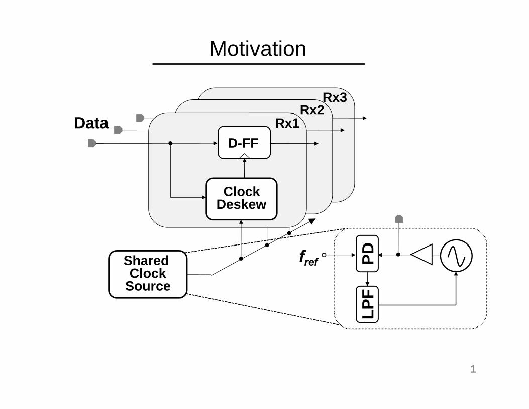
Data
Shared Clock
Source
ClockDeskew
D-FFRx3
ClockDeskew
D-FFRx2
ClockDeskew
D-FFRx1
PDLP
F
fref
Motivation
1
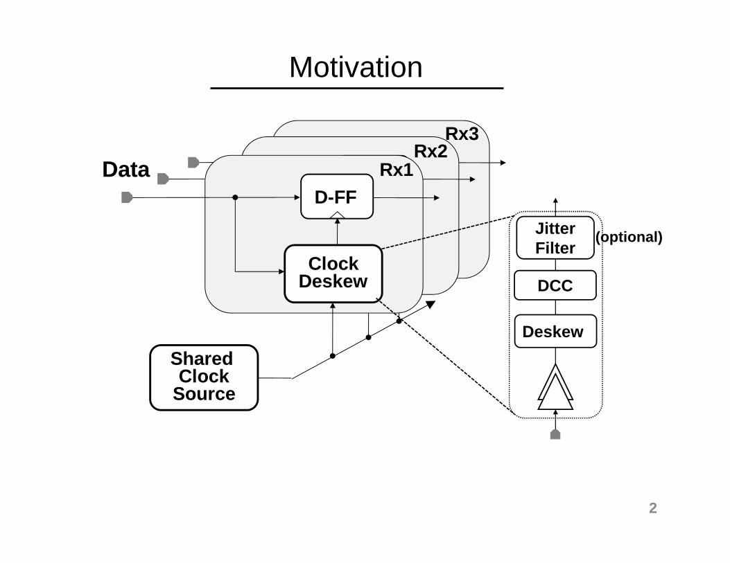
Data
Shared Clock
Source
ClockDeskew
D-FFRx3
ClockDeskew
D-FFRx2
ClockDeskew
D-FFRx1
Motivation
Deskew
JitterFilter
(optional)
DCC
2
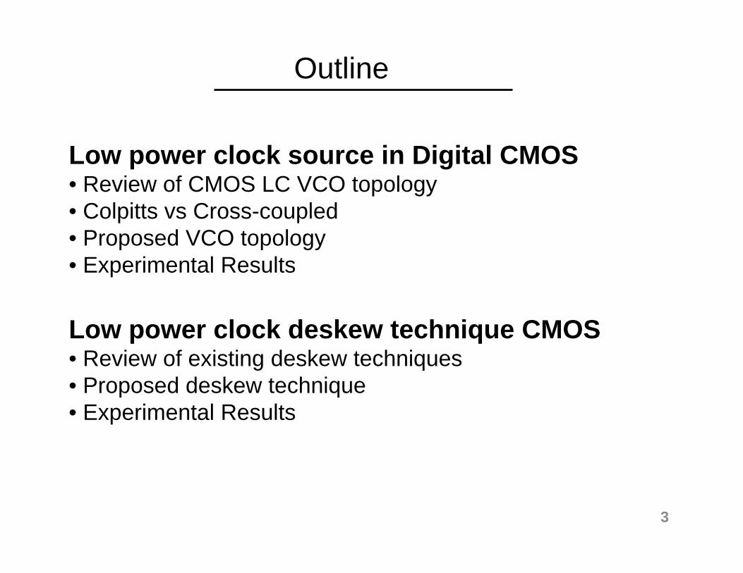
Low power clock source in Digital CMOS• Review of CMOS LC VCO topology• Colpitts vs Cross-coupled• Proposed VCO topology• Experimental Results
Low power clock deskew technique CMOS• Review of existing deskew techniques• Proposed deskew technique• Experimental Results
Outline
3
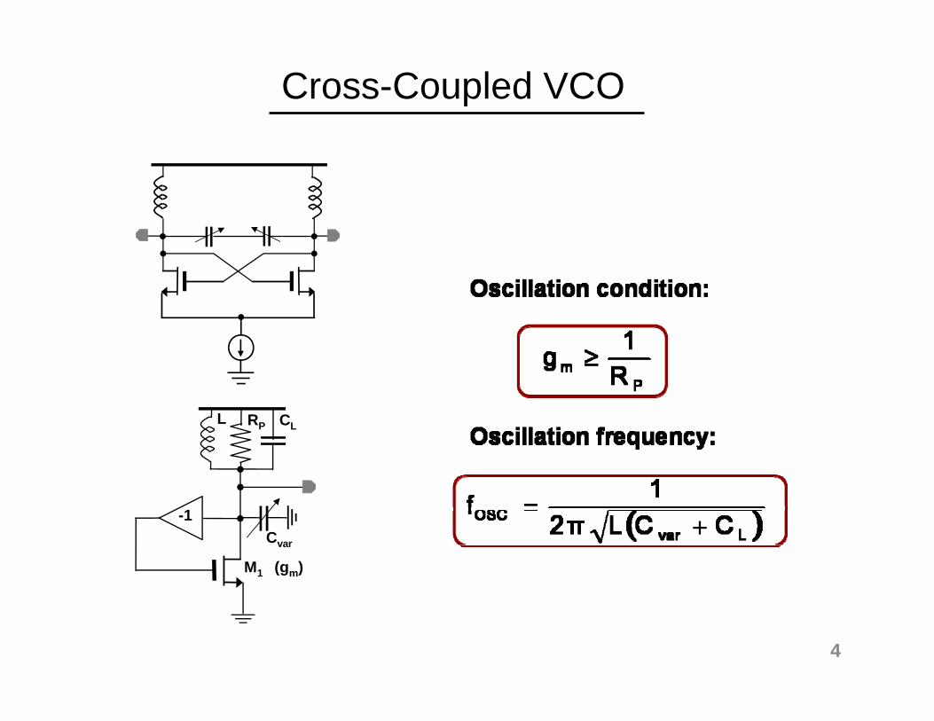
(gm)
CLRPL
M1
-1Cvar
Cross-Coupled VCO
4
RPL
C1
Cvar
CL
(gm)M1
Conventional Colpitts
RP
L
C1
M1
Cvar
RL CL
(gm)
[Nguyen’92]
Modified Colpitts
Decouples the tank from load
Colpitts VCO
5
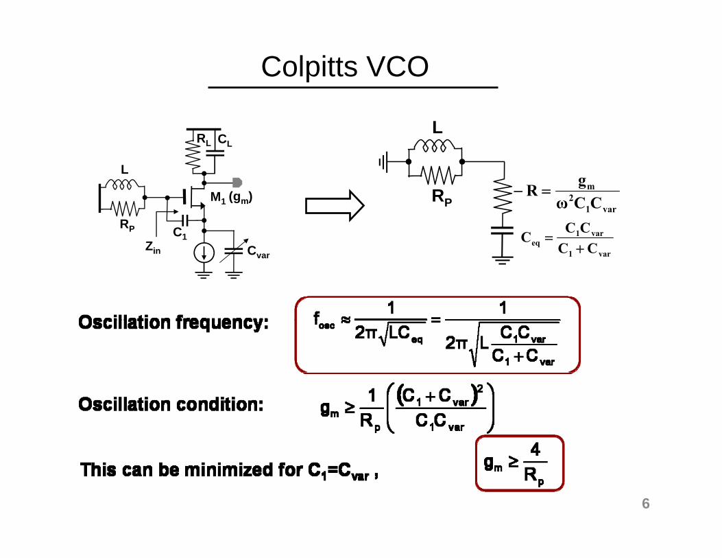
RP
L
C1
M1
Cvar
RL CL
(gm)
Zin
RP
L
var12
m
CCωgR =−
var1
var1eq CC
CCC+
=
Colpitts VCO
6
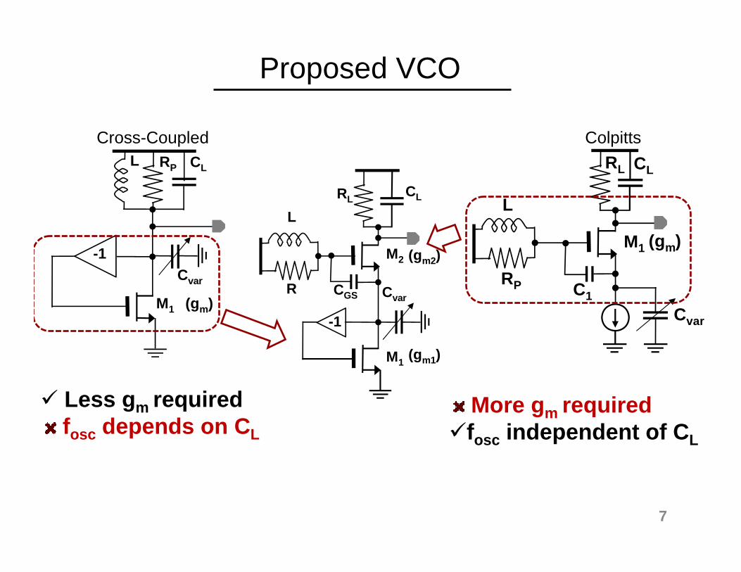
(gm)
CLRPL
M1
-1Cvar RP
L
C1
M1
Cvar
RL CL
(gm)
Less gm requiredfosc depends on CL
More gm requiredfosc independent of CL
R
CL
L
CGS
M2
M1
-1
Cvar
RL
(gm1)
(gm2)
Proposed VCO
Cross-Coupled Colpitts
7
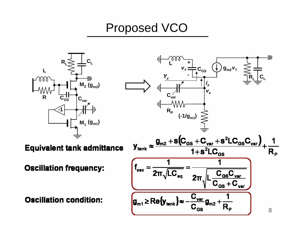
R
CL
L
CGS
M2
M1
-1
Cvar
RL
(gm1)
(gm2)Yx
RP
vx
v1
+
-ix
Cvar
(-1/gm1)
gm2v1L
CGS
RL CL
Proposed VCO
8
PR1
≥
1
var
var2−
⎟⎟⎠
⎞⎜⎜⎝
⎛
+=
CCCCLf
GS
GSosc π
( )( ) 1
var2−
+= Losc CCLf π
1
var1
var12−
⎟⎟⎠
⎞⎜⎜⎝
⎛
+=
CCCCLf osc π
PR4
≥
⎟⎟⎠
⎞⎜⎜⎝
⎛−≥ 2
var1m
GSP
gCC
R
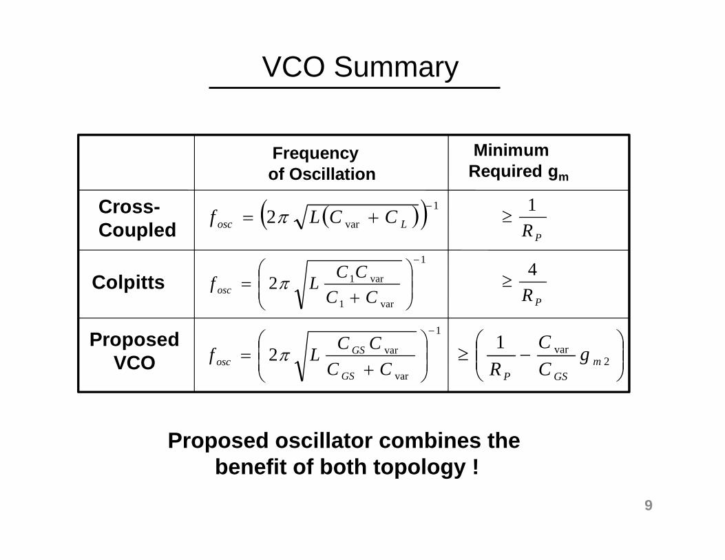
Frequencyof Oscillation
MinimumRequired gm
Cross-Coupled
Colpitts
ProposedVCO
Proposed oscillator combines the benefit of both topology !
VCO Summary
9
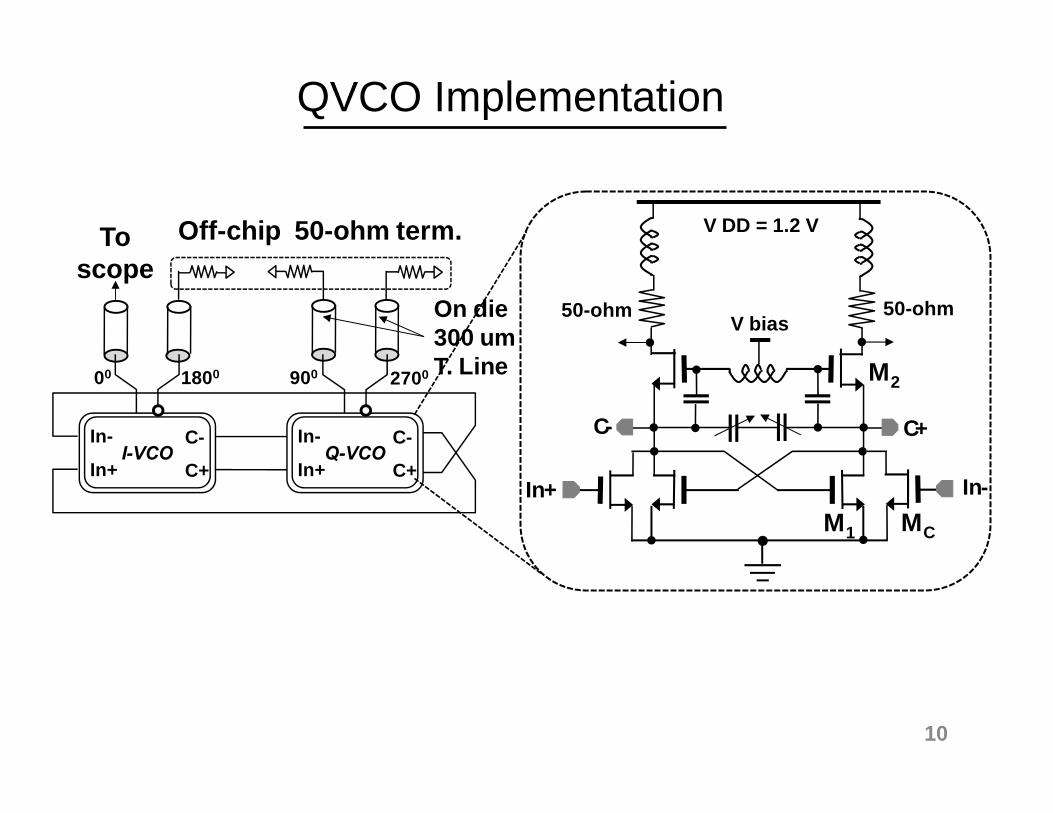
On die 300 um T. Line
To scope
I-VCOIn-
In+
C-
C+Q-VCO
In-
In+
C-
C+
00 1800 900 2700
Off-chip 50-ohm term.
In+
C+C-
M2
MCM1
In-
50-ohm 50-ohmV bias
V DD = 1.2 V
QVCO Implementation
10
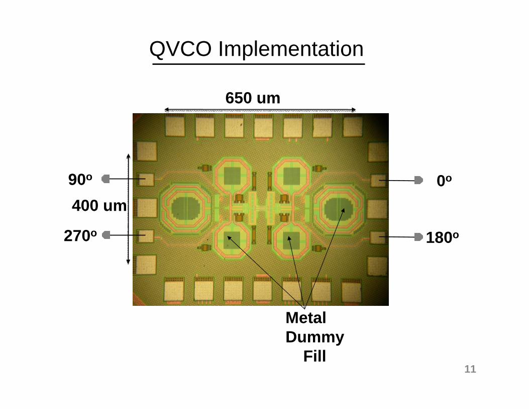
650 um
400 um
Metal Dummy
Fill
0o
180o270o
90o
QVCO Implementation
11
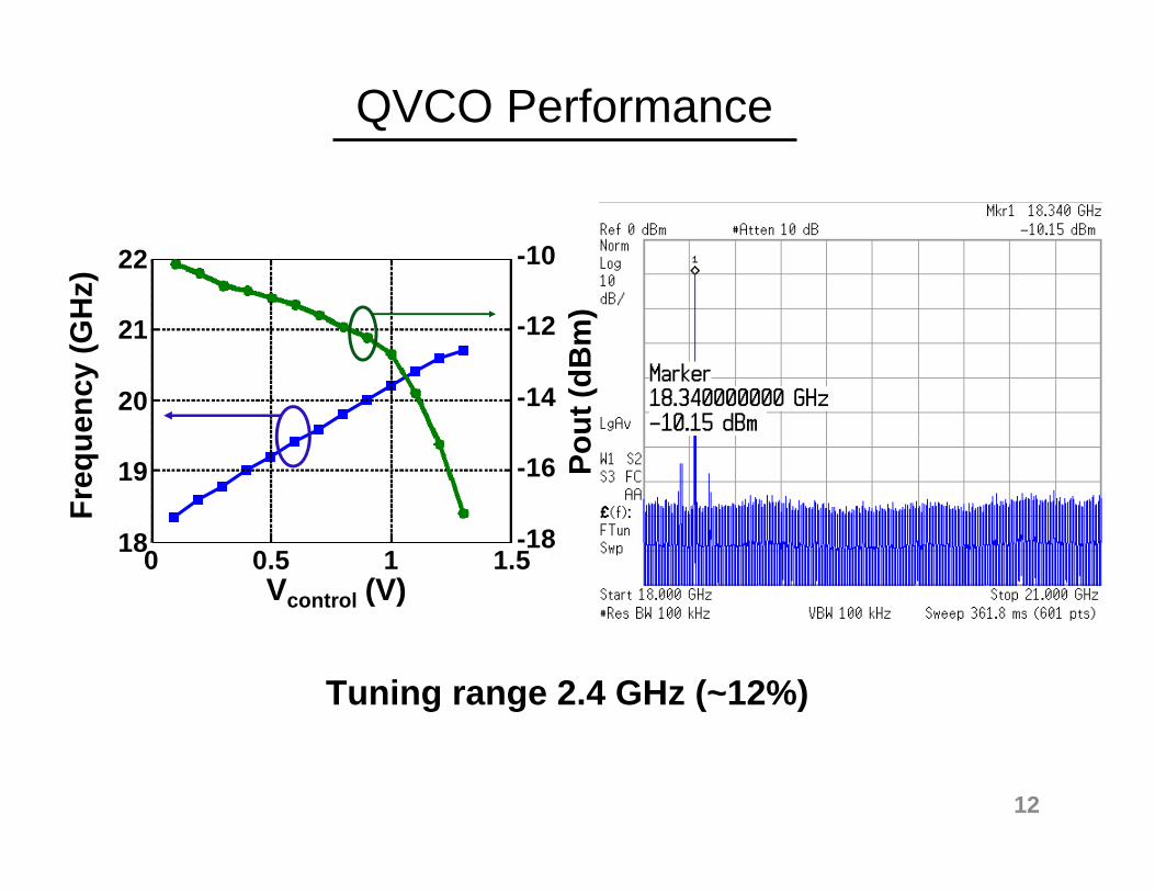
0 0.5 1 1.518
19
20
21
22
0-18
-16
-14
-12
-10
Vcontrol (V)
Freq
uenc
y (G
Hz)
Pout
(dB
m)
Tuning range 2.4 GHz (~12%)
QVCO Performance
12
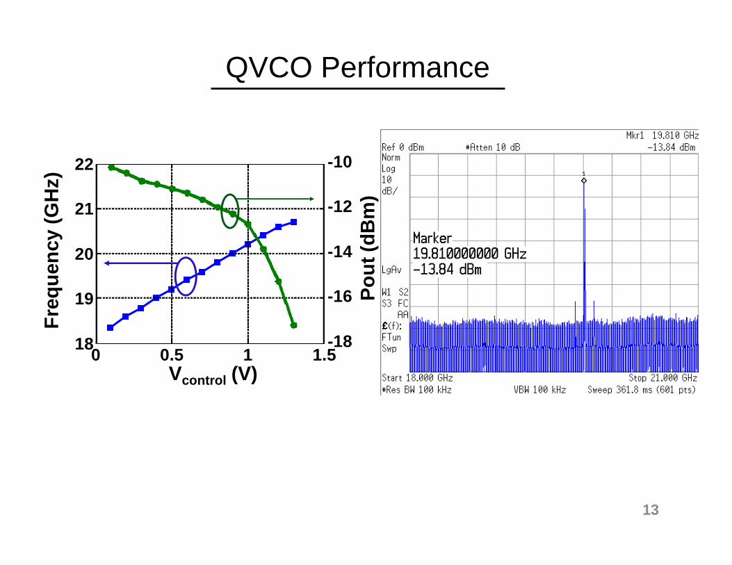
0 0.5 1 1.518
19
20
21
22
0-18
-16
-14
-12
-10
Vcontrol (V)
Freq
uenc
y (G
Hz)
Pout
(dB
m)
QVCO Performance
13
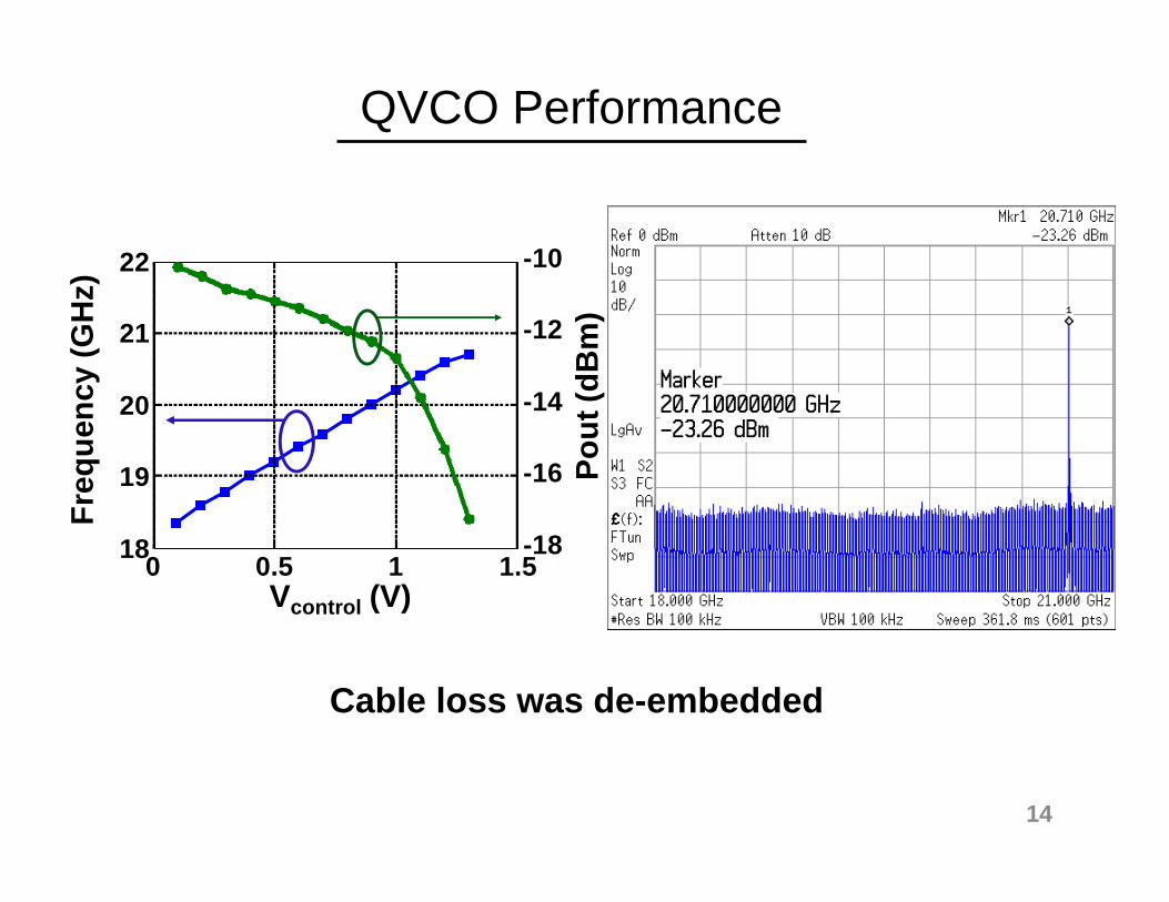
0 0.5 1 1.518
19
20
21
22
0-18
-16
-14
-12
-10
Vcontrol (V)
Freq
uenc
y (G
Hz)
Pout
(dB
m)
Cable loss was de-embedded
QVCO Performance
14
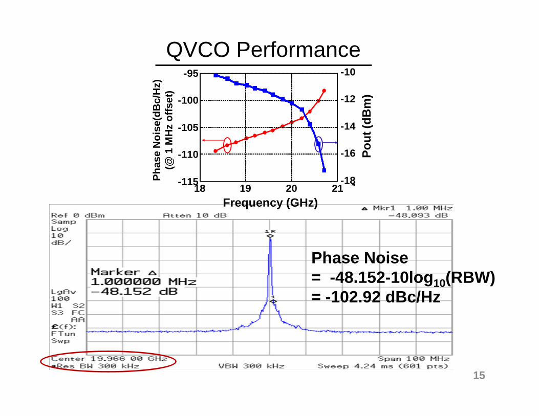
18 19 20 21-115
-110
-105
-100
-95
1-18
-16
-14
-12
-10
Phas
e N
oise
(dB
c/H
z)(@
1 M
Hz
offs
et)
Frequency (GHz)
Pout
(dB
m)
QVCO Performance
Phase Noise = -48.152-10log10(RBW) = -102.92 dBc/Hz
15
18 19 20 21-110
-105
-100
-95
Phas
e N
oise
(dB
c/H
z)(@
1 M
Hz
offs
et)
Frequency (GHz)
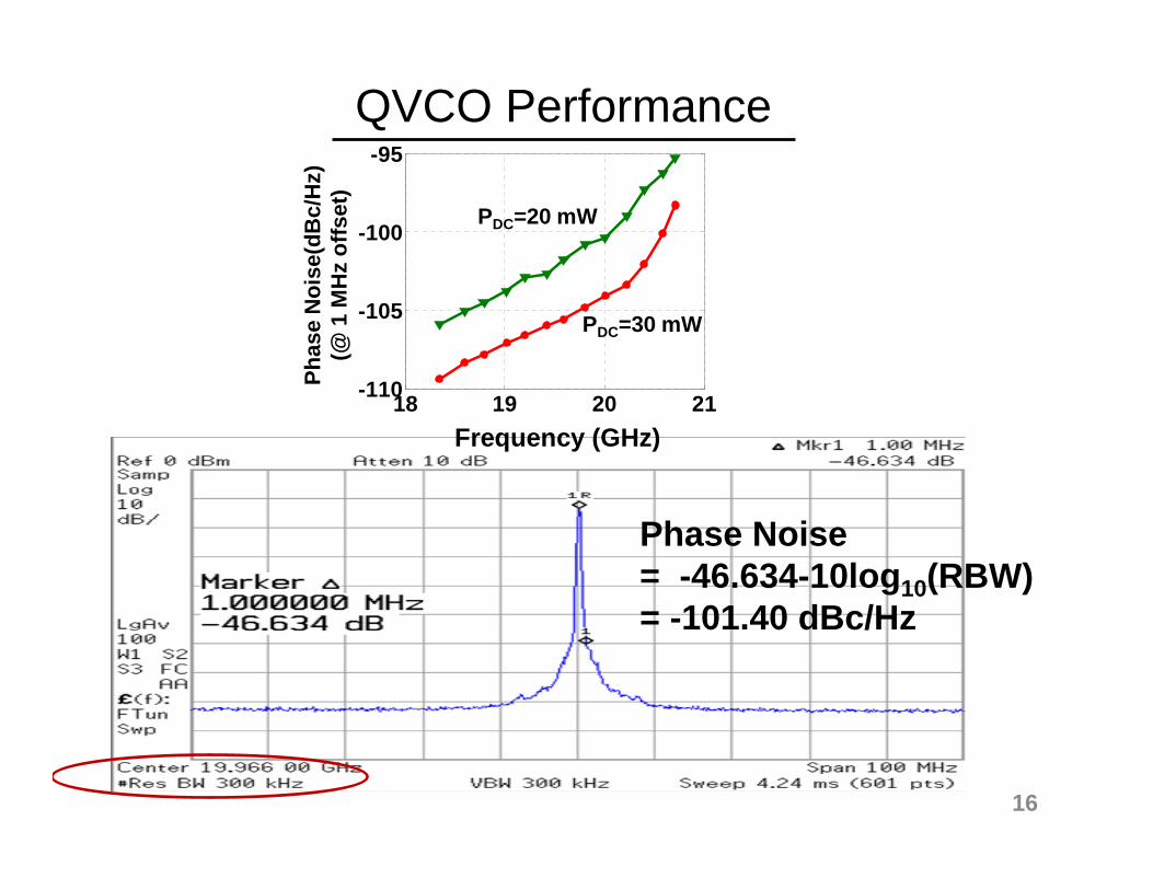
PDC=30 mW
PDC=20 mW
QVCO Performance
Phase Noise = -46.634-10log10(RBW) = -101.40 dBc/Hz
16
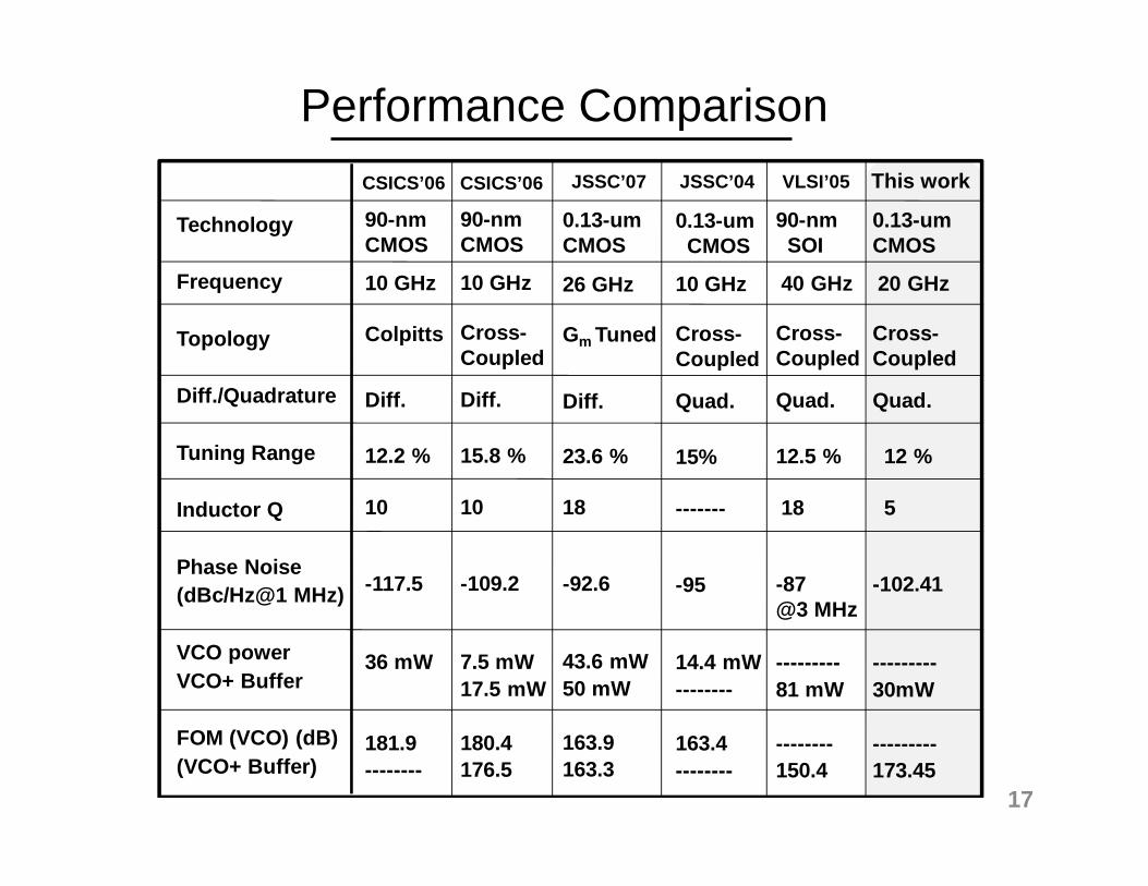
VLSI’05JSSC’07 JSSC’04
0.13-um CMOS
20 GHz
Cross-Coupled
Quad.
12 %
5
-102.41
---------30mW
---------173.45
Technology
Frequency
Topology
Diff./Quadrature
Tuning Range
Inductor Q
Phase Noise(dBc/Hz@1 MHz)
VCO powerVCO+ Buffer
FOM (VCO) (dB)(VCO+ Buffer)
90-nm CMOS
10 GHz
Colpitts
Diff.
12.2 %
10
-117.5
36 mW
181.9 --------
90-nm CMOS
10 GHz
Cross-Coupled
Diff.
15.8 %
10
-109.2
7.5 mW17.5 mW
180.4176.5
0.13-um CMOS
10 GHz
Cross-Coupled
Quad.
15%
-------
-95
14.4 mW--------
163.4--------
0.13-um CMOS
26 GHz
Gm Tuned
Diff.
23.6 %
18
-92.6
43.6 mW50 mW
163.9163.3
90-nm SOI
40 GHz
Cross-Coupled
Quad.
12.5 %
18
-87@3 MHz
---------81 mW
--------150.4
This workCSICS’06CSICS’06
Performance Comparison
17
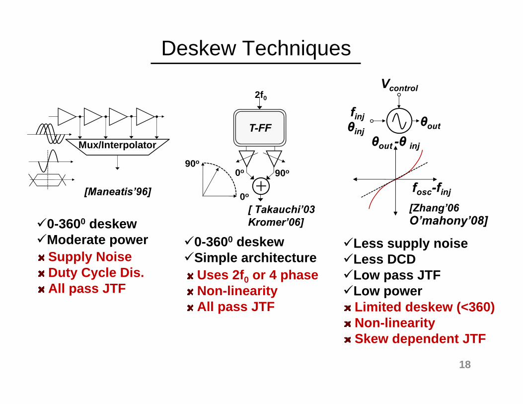
0-3600 deskewModerate powerSupply NoiseDuty Cycle Dis.All pass JTF
Mux/Interpolator
[Maneatis’96]
0-3600 deskewSimple architectureUses 2f0 or 4 phaseNon-linearityAll pass JTF
T-FF
2f0
0o 90o
0o
90o
[ Takauchi’03Kromer’06]
Less supply noiseLess DCDLow pass JTFLow powerLimited deskew (<360)Non-linearitySkew dependent JTF
finj
Vcontrol
θinjθout
θout -θ inj
fosc-finj
[Zhang’06O’mahony’08]
Deskew Techniques
18
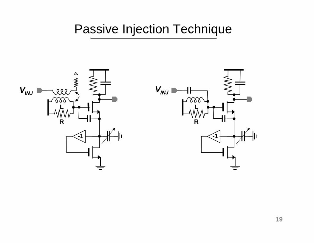
R
L
-1
VINJ
R
L
-1
VINJ
Passive Injection Technique
19
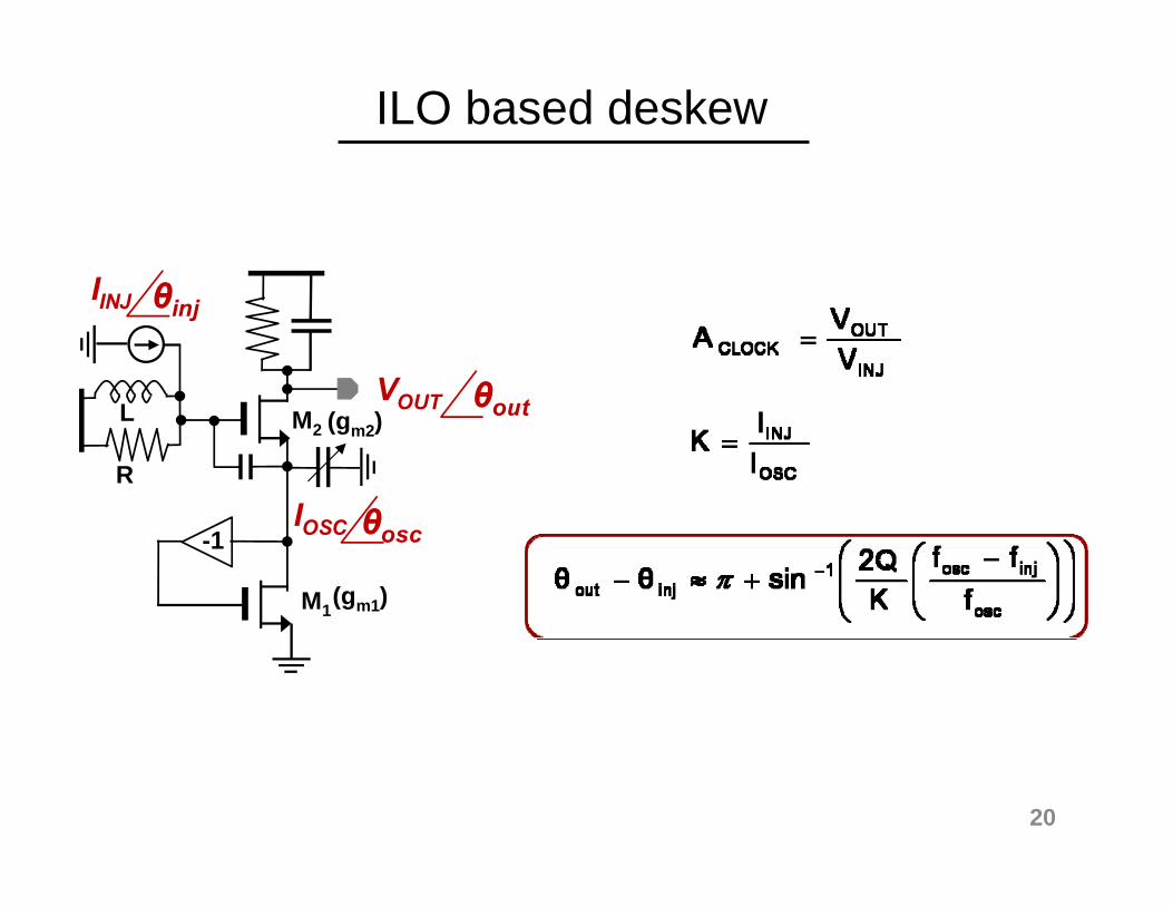
R
L M2
M1
-1
(gm1)
(gm2)VOUT θout
θinjIINJ
θoscIOSC
ILO based deskew
20
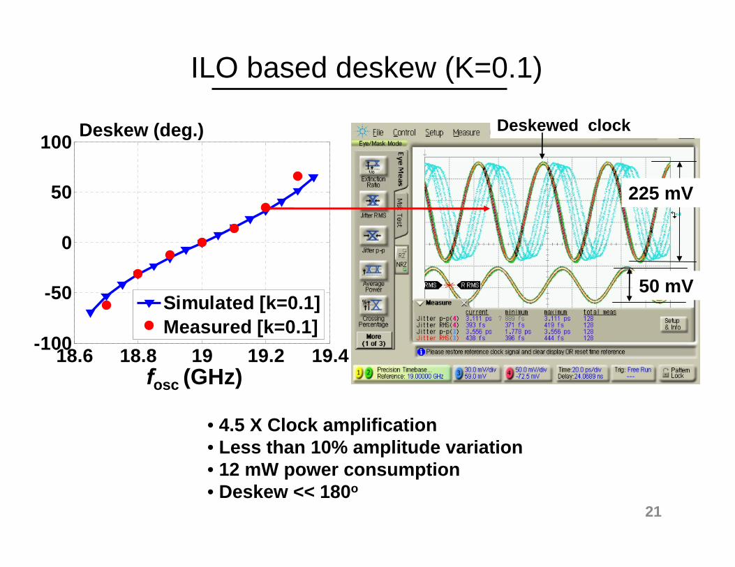
18.6 18.8 19 19.2 19.4-100
-50
0
50
100
Simulated [k=0.1]Measured [k=0.1]
fosc (GHz)
Deskew (deg.)
225 mV
50 mV
• 4.5 X Clock amplification• Less than 10% amplitude variation• 12 mW power consumption• Deskew << 180o
Deskewed clock
ILO based deskew (K=0.1)
21
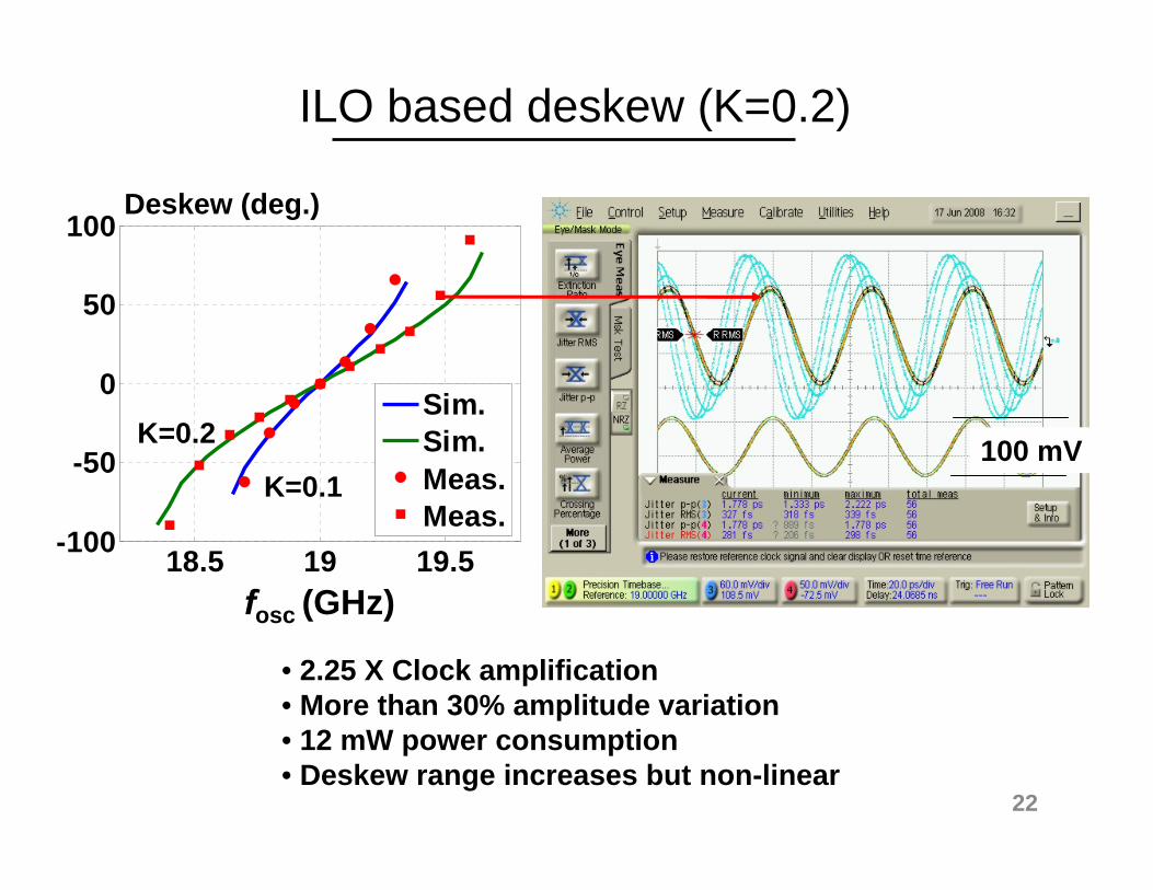
Deskew (deg.)
fosc (GHz)18.5 19 19.5-100
-50
0
50
100
Sim.Sim.Meas.Meas.
100 mVK=0.1
K=0.2
• 2.25 X Clock amplification• More than 30% amplitude variation• 12 mW power consumption• Deskew range increases but non-linear
ILO based deskew (K=0.2)
22
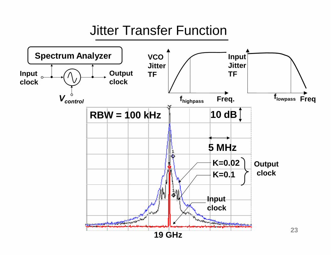
RBW = 100 kHz 10 dB
5 MHzK=0.02
19 GHz
Input clock
Vcontrol
Outputclock
Spectrum Analyzer VCO JitterTF
Freq.fhighpass
Input JitterTF
Freqflowpass
Jitter Transfer Function
Input clock
K=0.1Outputclock
23
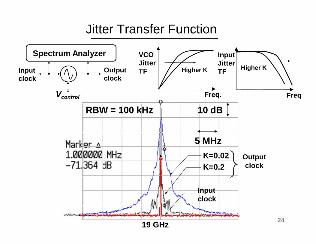
RBW = 100 kHz 10 dB
5 MHz
Input clock
K=0.02K=0.2
Outputclock
19 GHz
Input clock
Vcontrol
Outputclock
Spectrum Analyzer VCO JitterTF
Freq.
Higher K
Input JitterTF
Freq
Higher K
Jitter Transfer Function
24
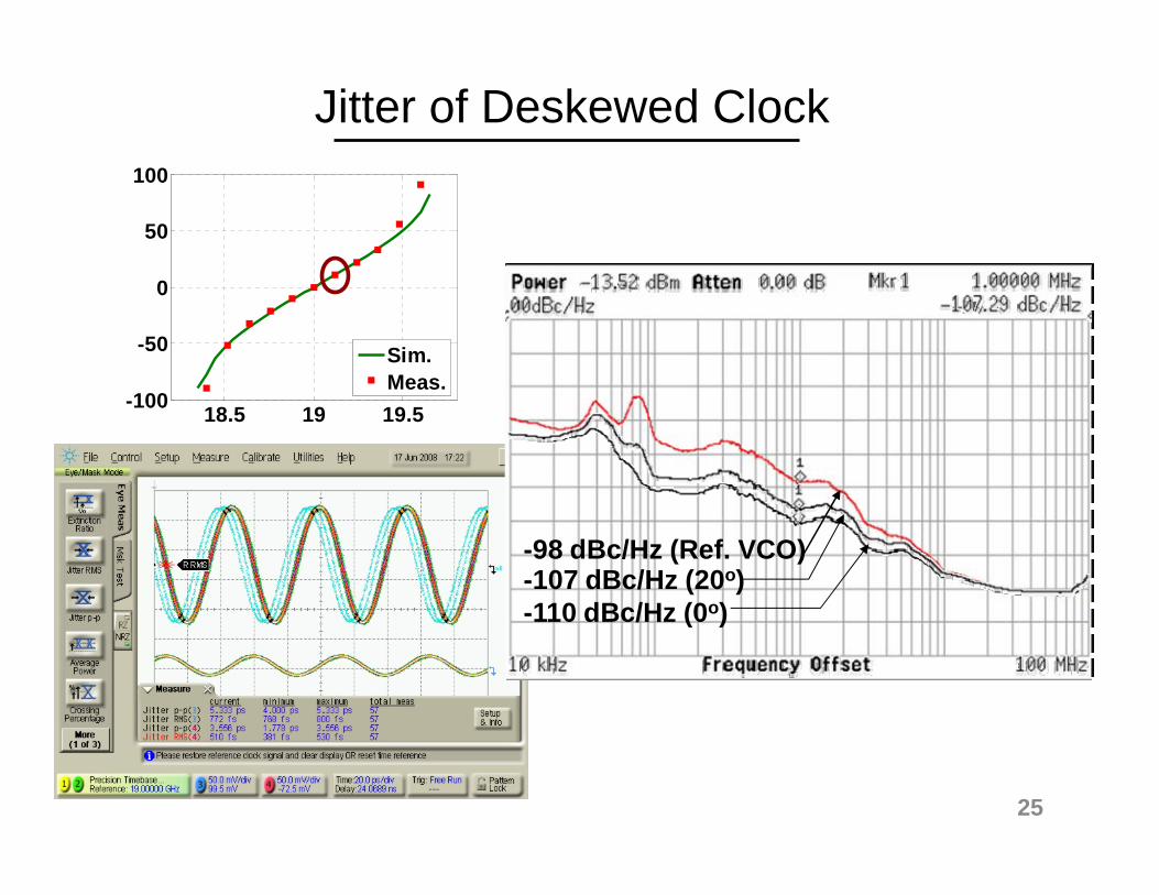
Jitter of Deskewed Clock
18.5 19 19.5-100
-50
0
50
100
Sim.Meas.
-98 dBc/Hz (Ref. VCO)-107 dBc/Hz (20o)-110 dBc/Hz (0o)
25
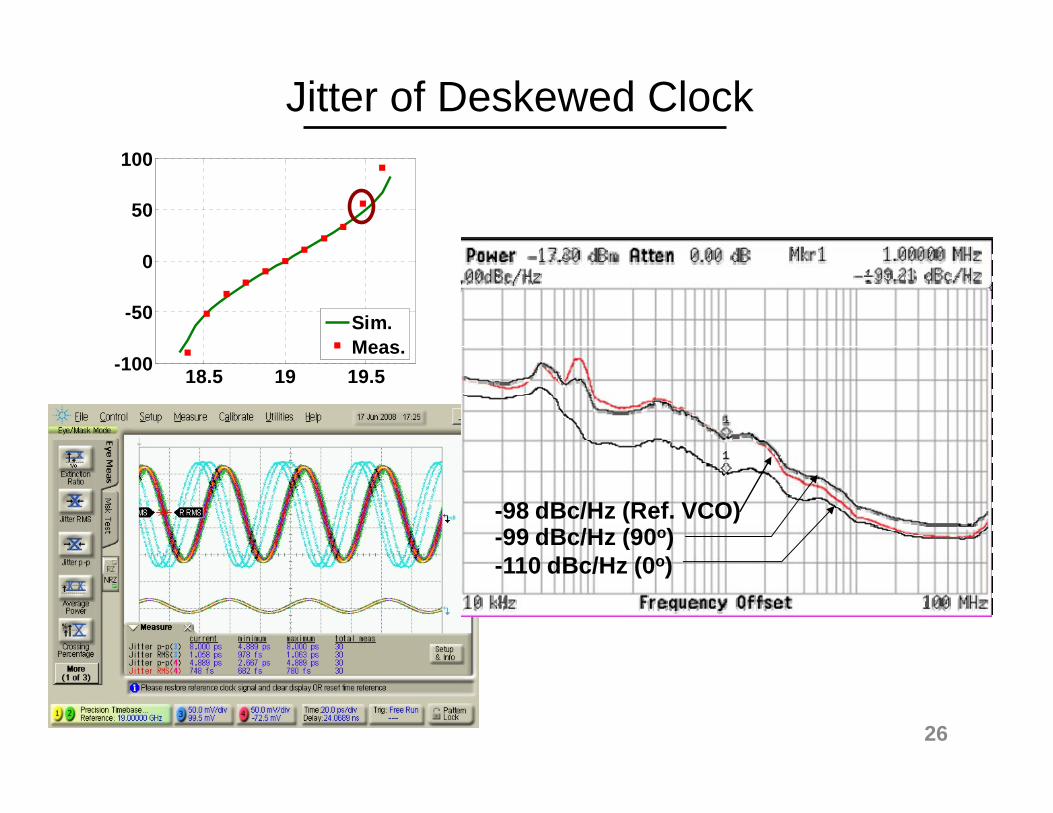
Jitter of Deskewed Clock
18.5 19 19.5-100
-50
0
50
100
Sim.Meas.
-98 dBc/Hz (Ref. VCO)-99 dBc/Hz (90o)-110 dBc/Hz (0o)
26
18.5 19 19.5-100
-50
0
50
100
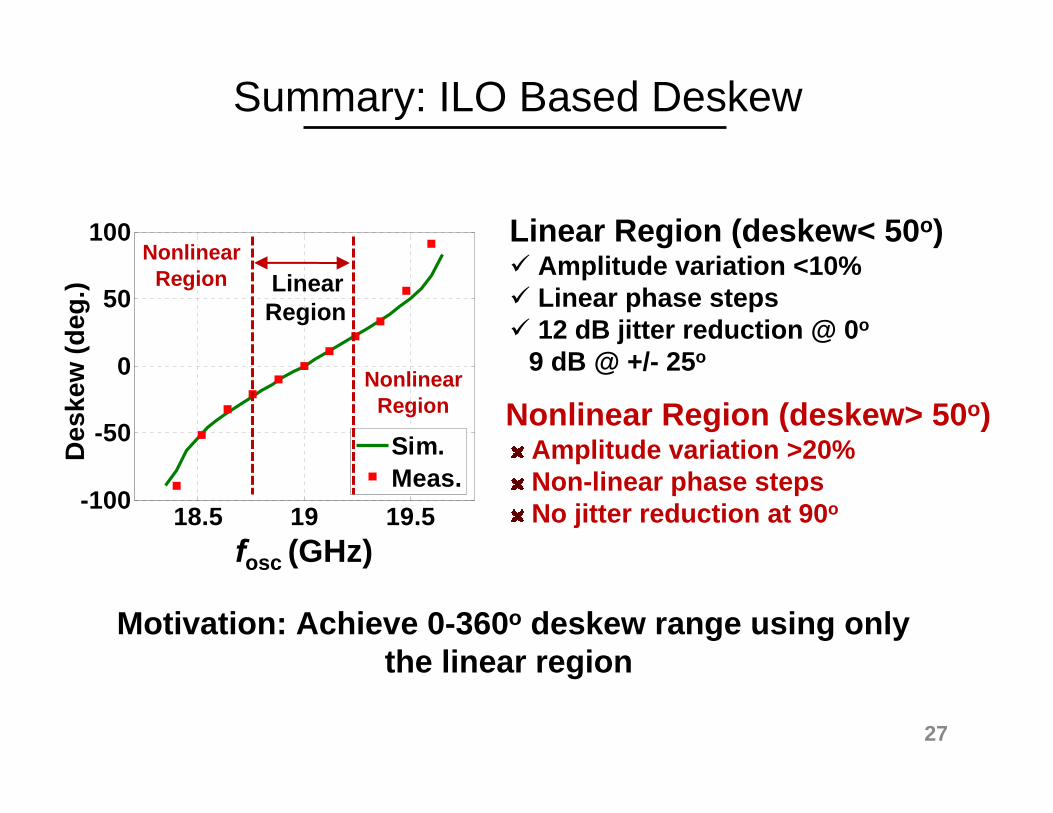
Sim.Meas.
Des
kew
(deg
.)
fosc (GHz)
Linear Region
Nonlinear Region
Nonlinear Region
Linear Region (deskew< 50o)Amplitude variation <10%Linear phase steps12 dB jitter reduction @ 0o
9 dB @ +/- 25o
Nonlinear Region (deskew> 50o)Amplitude variation >20%Non-linear phase stepsNo jitter reduction at 90o
Motivation: Achieve 0-360o deskew range using only the linear region
Summary: ILO Based Deskew
27
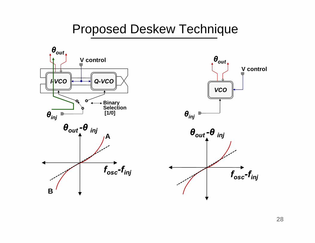
VCO
V control θout
θinj
θout -θ inj
fosc-finj
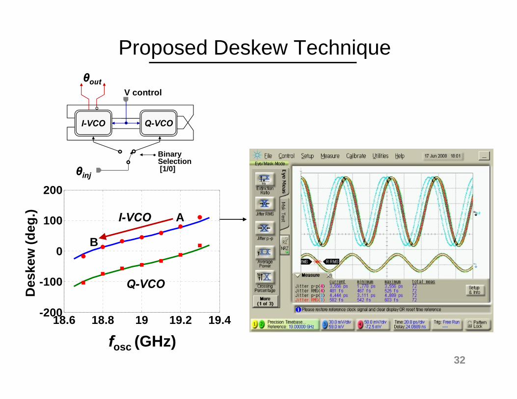
Proposed Deskew Technique
I-VCO
V control
Q-VCO
BinarySelection[1/0]
θout
θinj
θout -θ inj
fosc-finj
A
B
28
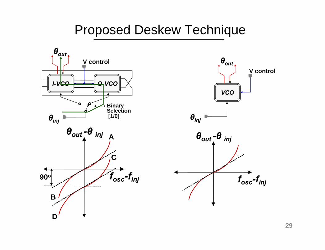
VCO
V control θout
θinj
θout -θ inj
fosc-finj
I-VCO
V control
Q-VCO
BinarySelection[1/0]
θout
θinj
θout -θ inj
fosc-finj90o
A
B
C
D
Proposed Deskew Technique
29
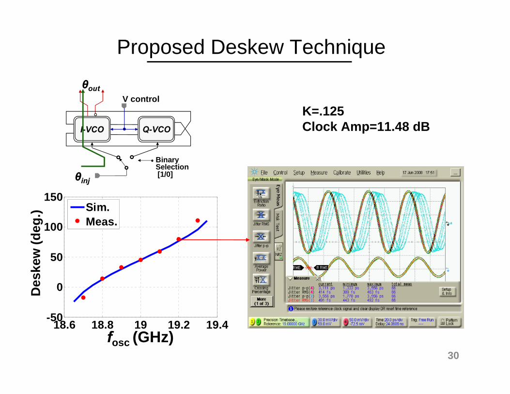
18.6 18.8 19 19.2 19.4-50
0
50
100
150Sim.Meas.
I-VCO
V control
Q-VCO
BinarySelection[1/0]
θout
θinj
fosc (GHz)
Des
kew
(deg
.)
K=.125Clock Amp=11.48 dB
Proposed Deskew Technique
30
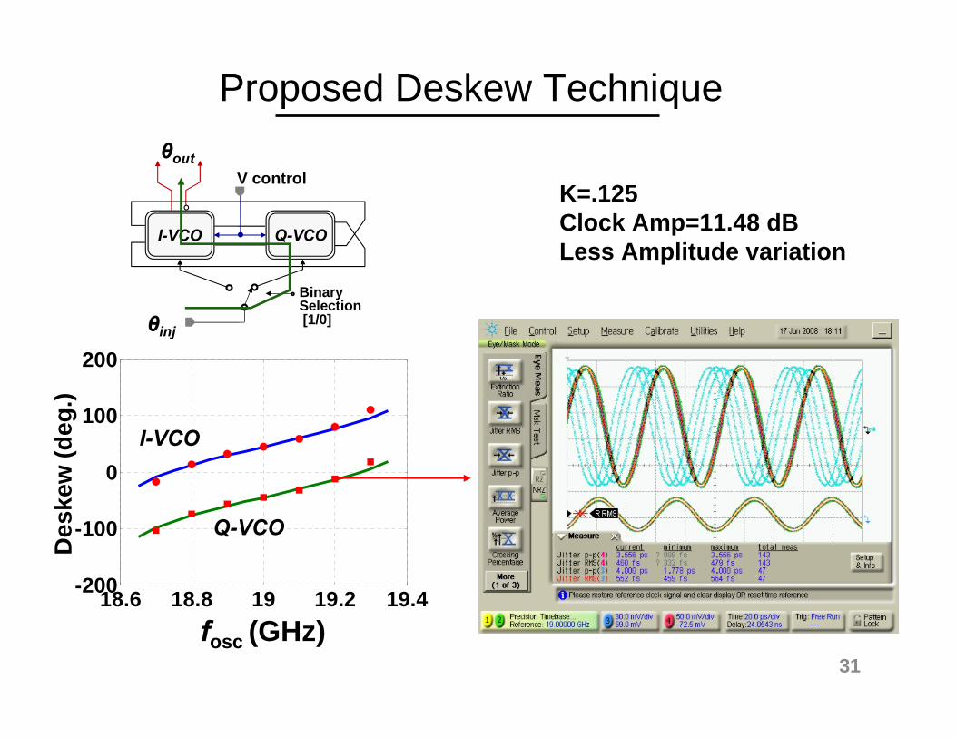
fosc (GHz)
Des
kew
(deg
.)
K=.125Clock Amp=11.48 dBLess Amplitude variation
18.6 18.8 19 19.2 19.4-200
-100
0
100
200
I-VCO
V control
Q-VCO
BinarySelection[1/0]
θout
θinj
I-VCO
Q-VCO
Proposed Deskew Technique
31
18.6 18.8 19 19.2 19.4-200
-100
0
100
200
I-VCO
V control
Q-VCO
BinarySelection[1/0]
θout
θinj
A
B
I-VCO
Q-VCODes
kew
(deg
.)
fosc (GHz)
Proposed Deskew Technique
32
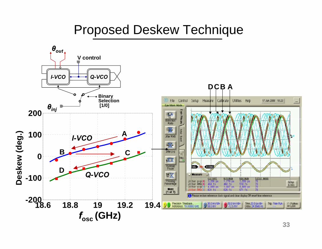
I-VCO
V control
Q-VCO
BinarySelection[1/0]
θout
θinj
AD BC
18.6 18.8 19 19.2 19.4-200
-100
0
100
200
A
B C
D
I-VCO
Q-VCO
Des
kew
(deg
.)
fosc (GHz)
Proposed Deskew Technique
33
18.6 18.8 19 19.2 19.4-200
-100
0
100
200
A
B C
D
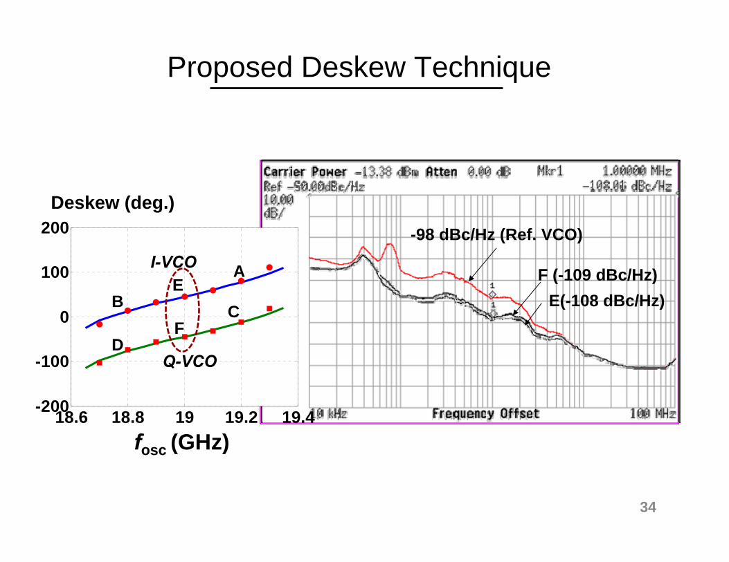
E
F
F (-109 dBc/Hz)E(-108 dBc/Hz)
-98 dBc/Hz (Ref. VCO)I-VCO
Q-VCO
Deskew (deg.)
fosc (GHz)
Proposed Deskew Technique
34
18.6 18.8 19 19.2 19.4-200
-100
0
100
200
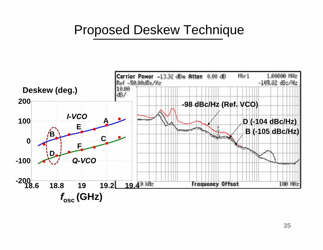
A
B C
D
E
F
I-VCO
Q-VCO
D (-104 dBc/Hz)B (-105 dBc/Hz)
-98 dBc/Hz (Ref. VCO)
fosc (GHz)
Deskew (deg.)
Proposed Deskew Technique
35
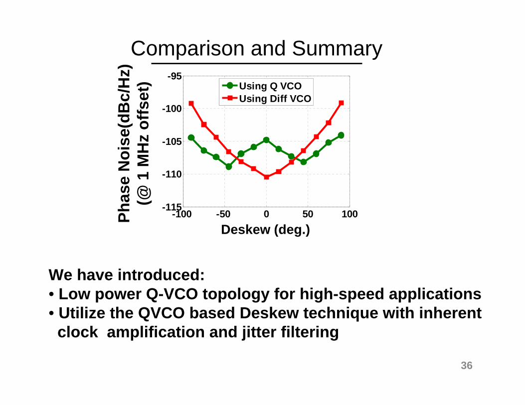
-100 -50 0 50 100-115
-110
-105
-100
-95Using Q VCOUsing Diff VCO
Phas
e N
oise
(dB
c/H
z)(@
1 M
Hz
offs
et)
Deskew (deg.)
Comparison and Summary
We have introduced: • Low power Q-VCO topology for high-speed applications• Utilize the QVCO based Deskew technique with inherent clock amplification and jitter filtering
36
Acknowledgements
•Intel Circuit Research Lab:F. O’Mahony, M. Mansuri & B. Casper for their contribution in clock deskew technique presented in this work
•Gennum Corporation:For providing design & fabrication facilities
37
39
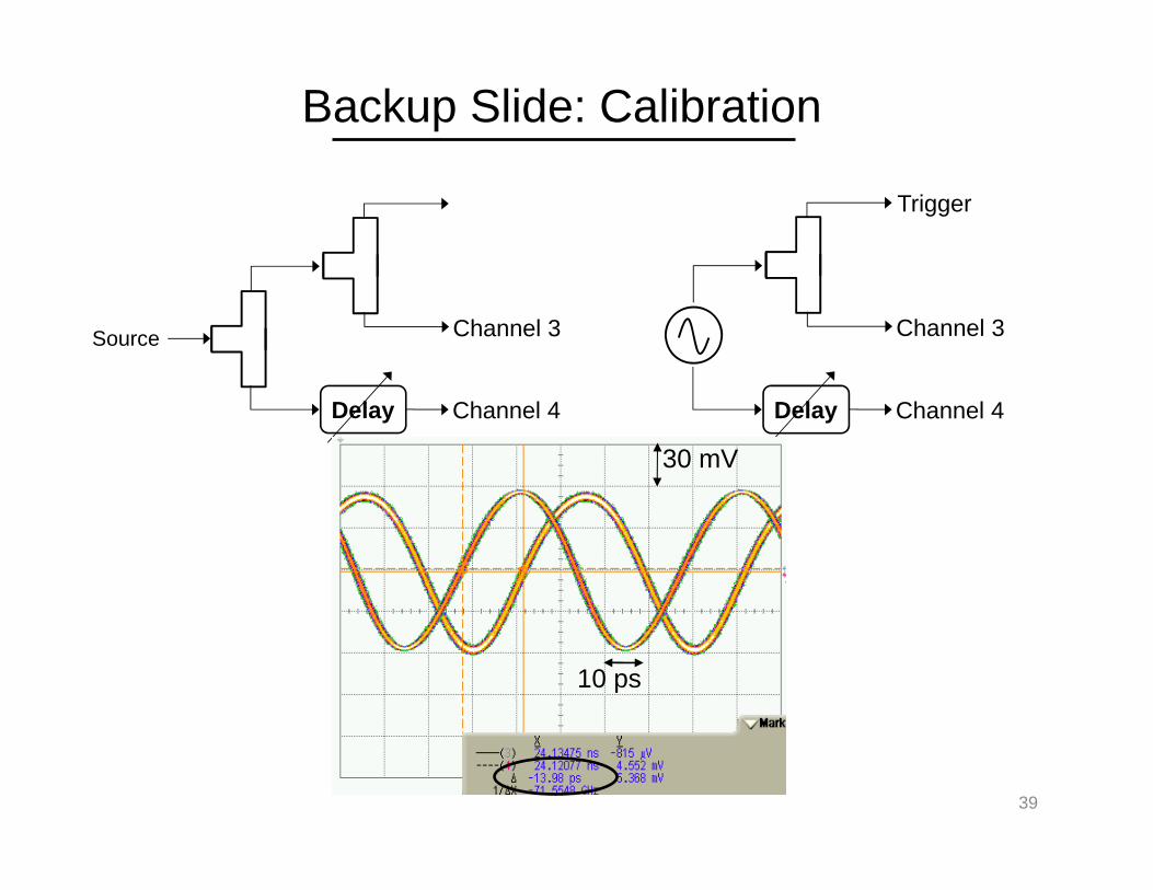
Backup Slide: Calibration
Trigger
Delay
Channel 3
Channel 4Delay
Channel 3
Channel 4
Source
10 ps
30 mV
40
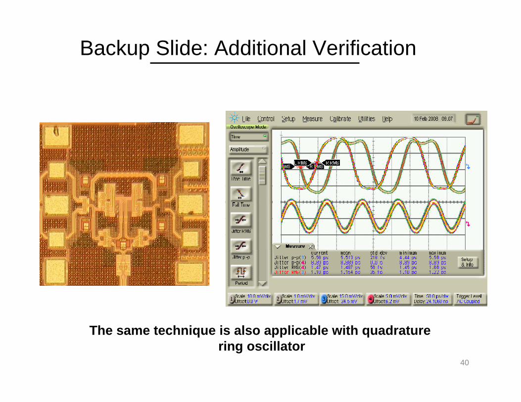
Backup Slide: Additional Verification
The same technique is also applicable with quadraturering oscillator