Embed Size (px)
Citation preview
NO
VE
MB
ER
21-
22
CanadaJapan
N A N OT E C H N O LO GY WO R K S H O P
2011

ii
1
Overview
To strengthen and celebrate the 25th anniversary of the Canada-Japan Agreement on Cooperation in Science and Technology, the Governments of Japan and Canada have proposed a bi-lateral workshop in nanotechnology. Leaders from both jurisdictions will be invited to a workshop hosted by the Waterloo Institute for Nanotechnology (WIN).
Nanotechnology is identifi ed in both countries as a priority area by the Expert Advisory Group (EAG) on Canada-Japan S&T Cooperation. Four major nanotechnology collaborations were recently identifi ed by the Embassies of Japan and Canada for their on-going execution of annual workshops, proven mobility and exchange programs, research funding and number of projects initiated. These are: (in order of MOU signing).
• National Institute for Nanotechnology (NINT) and National Institute of Advanced Industrial Science and Technology (AIST) – 2006
• NanoQuebec and Nagano Techno Foundation – 2009 • Waterloo Institute for Nanotechnology (WIN) and National
Institute for Materials Science (NIMS) – 2010 • McGill University and RIKEN – 2010
The Canada-Japan nanotechnology workshop is designed to bring Canadian and Japanese stakeholders together to highlight their success at a national and international level and for individual researcher teams to advance their collaborative projects. Scientists including Canadian Research Chairs in the fi eld of nanotechnology, government representatives and administrators from leading universities and nanotechnology organizations will be on hand to discuss the future of nanotechnology and recommend paths ahead.
By coming together we will help defi ne a nanotechnology road map for Canada and Japan cooperation that will identify future areas for research funding, commercialization and trade for our respective Governments and Embassies.
JAPAN COORDINATOR
Mr. Masahiro TakemuraGeneral Manager InternationalAff airs Offi ce PlanningDivision National Institutefor Materials Science
CANADA COORDINATOR
Mr. Alain Francq Managing Director Waterloo Institute for Nanotechnology University of Waterloo
2
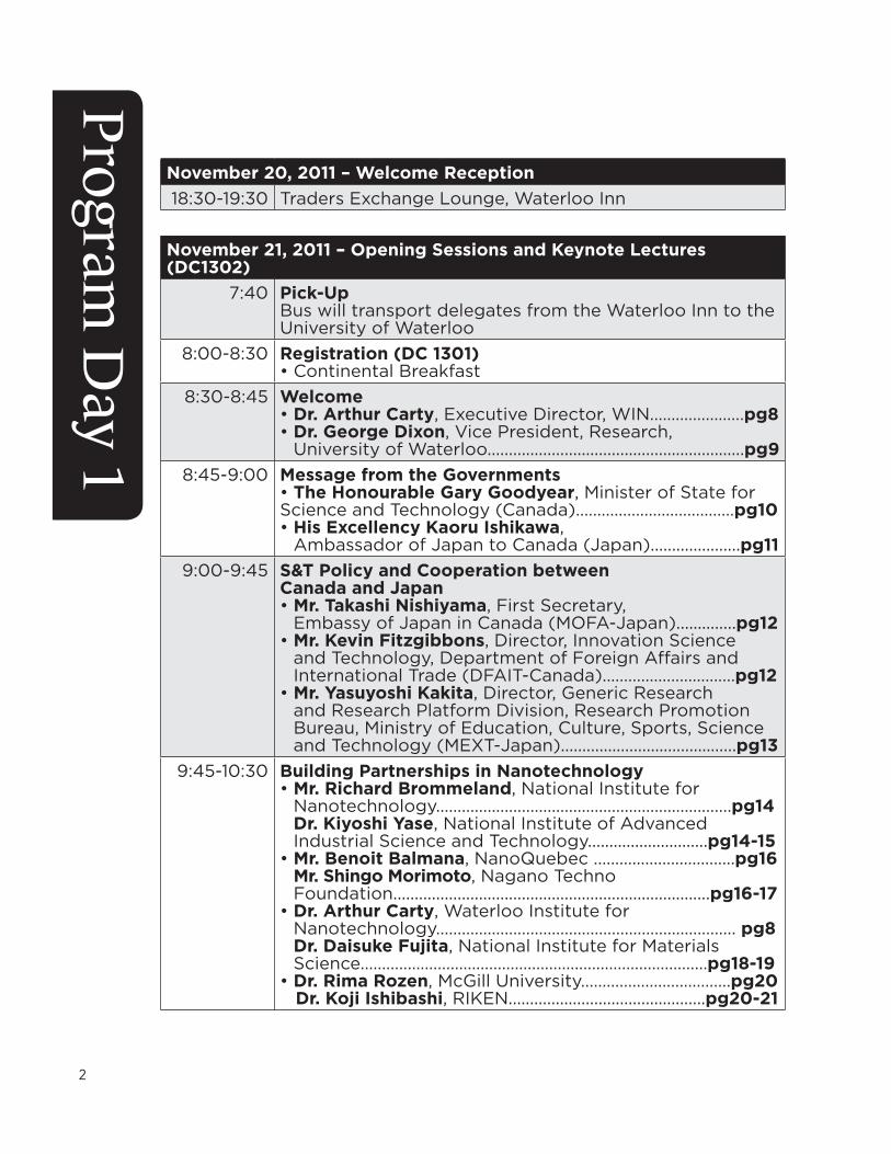
November 20, 2011 – Welcome Reception18:30-19:30 Traders Exchange Lounge, Waterloo Inn
November 21, 2011 – Opening Sessions and Keynote Lectures (DC1302)
7:40 Pick-UpBus will transport delegates from the Waterloo Inn to the University of Waterloo
8:00-8:30 Registration (DC 1301)• Continental Breakfast
8:30-8:45 Welcome• Dr. Arthur Carty, Executive Director, WIN......................pg8• Dr. George Dixon, Vice President, Research,
University of Waterloo............................................................pg98:45-9:00 Message from the Governments
• The Honourable Gary Goodyear, Minister of State for Science and Technology (Canada).....................................pg10• His Excellency Kaoru Ishikawa,
Ambassador of Japan to Canada (Japan).....................pg119:00-9:45 S&T Policy and Cooperation between
Canada and Japan• Mr. Takashi Nishiyama, First Secretary,
Embassy of Japan in Canada (MOFA-Japan)..............pg12• Mr. Kevin Fitzgibbons, Director, Innovation Science
and Technology, Department of Foreign Aff airs and International Trade (DFAIT-Canada)...............................pg12
• Mr. Yasuyoshi Kakita, Director, Generic Researchand Research Platform Division, Research Promotion Bureau, Ministry of Education, Culture, Sports, Science and Technology (MEXT-Japan).........................................pg13
9:45-10:30 Building Partnerships in Nanotechnology• Mr. Richard Brommeland, National Institute for
Nanotechnology.....................................................................pg14Dr. Kiyoshi Yase, National Institute of Advanced Industrial Science and Technology............................pg14-15
• Mr. Benoit Balmana, NanoQuebec .................................pg16Mr. Shingo Morimoto, Nagano Techno Foundation..........................................................................pg16-17
• Dr. Arthur Carty, Waterloo Institute for Nanotechnology...................................................................... pg8Dr. Daisuke Fujita, National Institute for Materials Science.................................................................................pg18-19
• Dr. Rima Rozen , McGill University...................................pg20 Dr. Koji Ishibashi, RIKEN..............................................pg20-21
Program D
ay 1

3
10:30-10:45 Break (DC 1301)10:45-11:45 Education Panel and Open Forum
Training the next generation of leaders innanoscience through international research.Chair - Dan Djukich, NanoAlberta......................................pg22• Ms. Jenny Reilly, Director, Canada-Japan Co-op
Program.....................................................................................pg22• Dr. Chris Barrett, McGill-RIKEN graduate exchange
program.....................................................................................pg23• Dr. Rudder Wu, International Center for Young
Scientists (ICYS), NIMS........................................................pg2411:45-12:00 NanoJapan 2012 Discussion
Mr.Charles-Anica Endo............................................................pg2412:00-13:00 Lunch (DC 1301)
Institution Introductions andScientifi c Talks from Delegation Leaders
13:00-13:30 Dr. Daisuke Fujita, Division Director,Advanced Key Technologies Division, NIMS..............pg18-19Mr. Masahiro Takemura, Chief Offi cer, Research and Analysis Offi ce, NIMS...............................................................pg25
13:30-14:00 Dr. Arthur Carty, Executive Director, WIN.........................pg814:00-14:30 Dr. Kiyoshi Yase, Director, Nanosystem Research
Institute, AIST........................................................................pg14-15Dr. Koichi Sakuta, Director, International Aff airsDivision, AIST.......................................................................pg26-27
14:30-15:00 Dr. Marie D’Iorio, Acting Director General, NINT..........pg2815:00-15:15 Break (DC 1301)15:15-15:45 Dr. Koji Ishibashi, Chief Scientist,
Advanced Device Laboratory, RIKEN.........................pg20-2115:45-16:15 Dr. Christopher Barrett, Associate Professor, Department
of Chemistry................................................................................pg23Dr. Zetian Mi, William Dawson Scholar, Electrical and Computer Engineering, McGill................pg28
16:15-16:30 Mr. Hiroyuki Hayashi, Director General, (NTF)..............pg2916:30-17:00 Dr. Toshihiro Hirai, Dean, Faculty of Textile
Science and Technology, Shinshu University............pg30-3117:00-17:30 Mr. Benoit Balmana, Interim Managing Director,
NanoQuebec................................................................................pg16Dr. Jerome Claverie, Director, Quebec Center for Functional Materials (CQMF), UQAM..........................pg31
17:30-18:00 Reception – University Club18:00-20:00 Dinner – University Club
4
Program D
ay 2
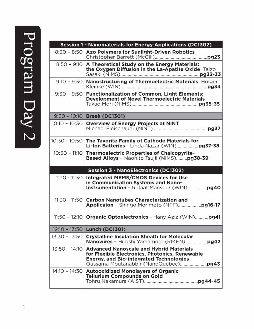
Session 1 - Nanomaterials for Energy Applications (DC1302)8:30 – 8:50 Azo Polymers for Sunlight-Driven Robotics
Christopher Barrett (McGill)...........................................pg238:50 – 9:10 A Theoretical Study on the Energy Materials:
the Oxygen Diff usion in the La-Apatite Oxide Taizo Sasaki (NIMS).................................................................pg32-33
9:10 – 9:30 Nanostructuring of Thermoelectric Materials Holger Kleinke (WIN).......................................................................pg34
9:30 – 9:50 Functionalization of Common, Light Elements; Development of Novel Thermoelectric Materials Takao Mori (NIMS).......................................................pg35-35
9:50 – 10:10 Break (DC1301)10:10 – 10:30 Overview of Energy Projects at NINT
Michael Fleischauer (NINT).............................................pg37
10:30 - 10:50 The Tavorite Family of Cathode Materials for Li-Ion Batteries - Linda Nazar (WIN)..................pg37-38
10:50 – 11:10 Thermoelectric Properties of Chalcopyrite-Based Alloys – Naohito Tsujii (NIMS).........pg38-39
Session 3 - NanoElectronics (DC1302)11:10 - 11:30 Integrated MEMS/CMOS Devices for Use
in Communication Systems and Nano-Instrumentation – Rafaat Mansour (WIN)................pg40
11:30 - 11:50 Carbon Nanotubes Characterization and Applicaion – Shingo Morimoto (NTF)...................pg16-17
11:50 – 12:10 Organic Optoelectronics - Hany Aziz (WIN)...........pg41
12:10 – 13:30 Lunch (DC1301)13:30 – 13:50 Crystalline Insulation Sheath for Molecular
Nanowires – Hiroshi Yamamoto (RIKEN)..................pg4213:50 – 14:10 Advanced Nanoscale and Hybrid Materials
for Flexible Electronics, Photonics, RenewableEnergy, and Bio-integrated Technologies Oussama Moutanabbir (NanoQuebec)......................pg43
14:10 – 14:30 Autooxidized Monolayers of OrganicTellurium Compounds on Gold Tohru Nakamura (AIST)............................................pg44-45
5
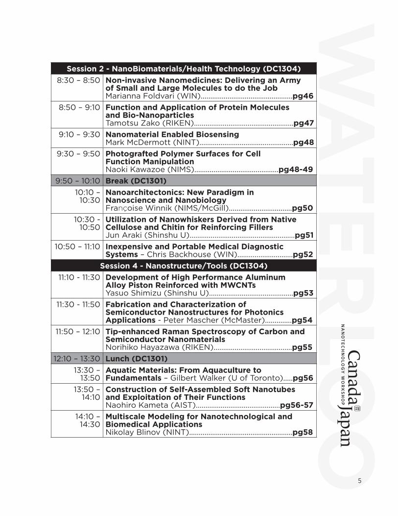
Session 2 - NanoBiomaterials/Health Technology (DC1304)8:30 – 8:50 Non-invasive Nanomedicines: Delivering an Army
of Small and Large Molecules to do the Job Marianna Foldvari (WIN)................................................pg46
8:50 – 9:10 Function and Application of Protein Moleculesand Bio-Nanoparticles Tamotsu Zako (RIKEN)....................................................pg47
9:10 – 9:30 Nanomaterial Enabled Biosensing Mark McDermott (NINT).................................................pg48
9:30 – 9:50 Photografted Polymer Surfaces for CellFunction Manipulation Naoki Kawazoe (NIMS)............................................pg48-49
9:50 – 10:10 Break (DC1301)10:10 – 10:30
Nanoarchitectonics: New Paradigm inNanoscience and Nanobiology Françoise Winnik (NIMS/McGill).................................pg50
10:30 - 10:50
Utilization of Nanowhiskers Derived from Native Cellulose and Chitin for Reinforcing Fillers Jun Araki (Shinshu U).......................................................pg51
10:50 – 11:10 Inexpensive and Portable Medical Diagnostic Systems – Chris Backhouse (WIN).............................pg52
Session 4 - Nanostructure/Tools (DC1304)11:10 - 11:30 Development of High Performance Aluminum
Alloy Piston Reinforced with MWCNTs Yasuo Shimizu (Shinshu U)............................................pg53
11:30 - 11:50 Fabrication and Characterization of Semiconductor Nanostructures for PhotonicsApplications - Peter Mascher (McMaster)..............pg54
11:50 – 12:10 Tip-enhanced Raman Spectroscopy of Carbon and Semiconductor Nanomaterials Norihiko Hayazawa (RIKEN).........................................pg55
12:10 – 13:30 Lunch (DC1301)13:30 –
13:50Aquatic Materials: From Aquaculture to Fundamentals – Gilbert Walker (U of Toronto).....pg56
13:50 – 14:10
Construction of Self-Assembled Soft Nanotubesand Exploitation of Their Functions Naohiro Kameta (AIST)............................................pg56-57
14:10 – 14:30
Multiscale Modeling for Nanotechnological and Biomedical Applications Nikolay Blinov (NINT)......................................................pg58
6
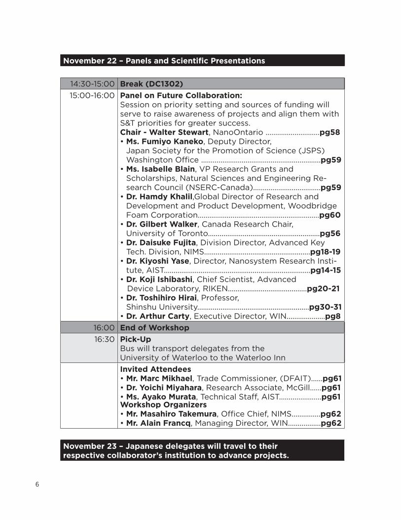
November 22 – Panels and Scientifi c Presentations
14:30-15:00 Break (DC1302)15:00-16:00 Panel on Future Collaboration:
Session on priority setting and sources of funding will serve to raise awareness of projects and align them with S&T priorities for greater success.Chair - Walter Stewart, NanoOntario ............................pg58• Ms. Fumiyo Kaneko, Deputy Director,
Japan Society for the Promotion of Science (JSPS) Washington Offi ce ..............................................................pg59
• Ms. Isabelle Blain, VP Research Grants andScholarships, Natural Sciences and Engineering Re-search Council (NSERC-Canada)...................................pg59
• Dr. Hamdy Khalil,Global Director of Research and Development and Product Development, Woodbridge Foam Corporation...............................................................pg60
• Dr. Gilbert Walker, Canada Research Chair,University of Toronto..........................................................pg56
• Dr. Daisuke Fujita, Division Director, Advanced Key Tech. Division, NIMS.......................................................pg18-19
• Dr. Kiyoshi Yase, Director, Nanosystem Research Insti-tute, AIST............................................................................pg14-15
• Dr. Koji Ishibashi, Chief Scientist, Advanced Device Laboratory, RIKEN.........................................pg20-21• Dr. Toshihiro Hirai, Professor,
Shinshu University..........................................................pg30-31• Dr. Arthur Carty, Executive Director, WIN....................pg8
16:00 End of Workshop16:30 Pick-Up
Bus will transport delegates from the University of Waterloo to the Waterloo InnInvited Attendees• Mr. Marc Mikhael, Trade Commissioner, (DFAIT)......pg61• Dr. Yoichi Miyahara, Research Associate, McGill......pg61• Ms. Ayako Murata, Technical Staff , AIST......................pg61Workshop Organizers• Mr. Masahiro Takemura, Offi ce Chief, NIMS...............pg62• Mr. Alain Francq, Managing Director, WIN.................pg62
November 23 – Japanese delegates will travel to theirrespective collaborator’s institution to advance projects.
7
NOTES:
AIST - National Institute of Advanced Industrial Science and Technology DFAIT - Department of Foreign Aff airs and International Trade Canada JSPS - Japan Society for the Promotion of Science McGill - McGill University MEXT - Ministry of Education, Culture, Sports, Science and TechnologyMOFA - Ministry of Foreign Aff airs of JapanNIMS - National Institute for Materials ScienceNINT - National Institute for Nanotechnology
NSERC - Natural Sciences and Engineering Research Council of CanadaNTF - Nagano Techno Foundation
Shinshu- Shinshu UniversityUQAM - University of Quebec at Montreal
WIN - Waterloo Institute for Nanotechnology
8
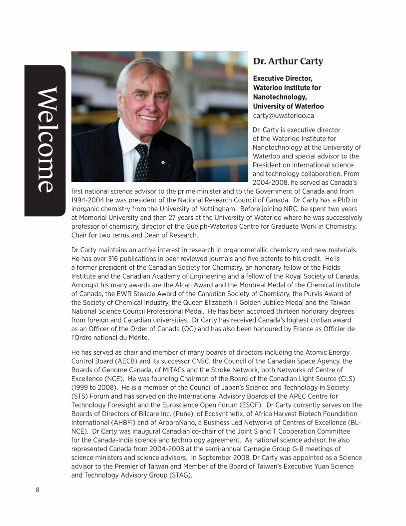
Dr. Carty is executive director of the Waterloo Institute for Nanotechnology at the University of Waterloo and special advisor to the President on international science and technology collaboration. From 2004-2008, he served as Canada’s
fi rst national science advisor to the prime minister and to the Government of Canada and from 1994-2004 he was president of the National Research Council of Canada. Dr Carty has a PhD in inorganic chemistry from the University of Nottingham. Before joining NRC, he spent two years at Memorial University and then 27 years at the University of Waterloo where he was successively professor of chemistry, director of the Guelph-Waterloo Centre for Graduate Work in Chemistry, Chair for two terms and Dean of Research.
Dr Carty maintains an active interest in research in organometallic chemistry and new materials. He has over 316 publications in peer reviewed journals and fi ve patents to his credit. He is a former president of the Canadian Society for Chemistry, an honorary fellow of the Fields Institute and the Canadian Academy of Engineering and a fellow of the Royal Society of Canada. Amongst his many awards are the Alcan Award and the Montreal Medal of the Chemical Institute of Canada, the EWR Steacie Award of the Canadian Society of Chemistry, the Purvis Award of the Society of Chemical Industry, the Queen Elizabeth II Golden Jubilee Medal and the Taiwan National Science Council Professional Medal. He has been accorded thirteen honorary degrees from foreign and Canadian universities. Dr Carty has received Canada’s highest civilian award as an Offi cer of the Order of Canada (OC) and has also been honoured by France as Offi cier de l’Ordre national du Mérite.
He has served as chair and member of many boards of directors including the Atomic Energy Control Board (AECB) and its successor CNSC, the Council of the Canadian Space Agency, the Boards of Genome Canada, of MITACs and the Stroke Network, both Networks of Centre of Excellence (NCE). He was founding Chairman of the Board of the Canadian Light Source (CLS) (1999 to 2008). He is a member of the Council of Japan’s Science and Technology in Society (STS) Forum and has served on the International Advisory Boards of the APEC Centre for Technology Foresight and the Euroscience Open Forum (ESOF). Dr Carty currently serves on the Boards of Directors of Bilcare Inc. (Pune), of Ecosynthetix, of Africa Harvest Biotech Foundation International (AHBFI) and of ArboraNano, a Business Led Networks of Centres of Excellence (BL-NCE). Dr Carty was inaugural Canadian co-chair of the Joint S and T Cooperation Committee for the Canada-India science and technology agreement. As national science advisor, he also represented Canada from 2004-2008 at the semi-annual Carnegie Group G-8 meetings of science ministers and science advisors. In September 2008, Dr Carty was appointed as a Science advisor to the Premier of Taiwan and Member of the Board of Taiwan’s Executive Yuan Science and Technology Advisory Group (STAG).
Dr. Arthur Carty
Executive Director,
Waterloo Institute for
Nanotechnology,
University of Waterloo
Welcom
e
9
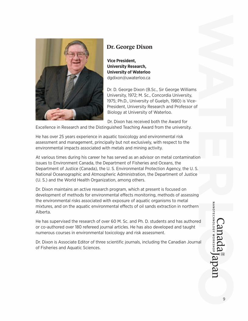
Dr. D. George Dixon (B.Sc., Sir George Williams University, 1972; M. Sc., Concordia University, 1975; Ph.D., University of Guelph, 1980) is Vice-President, University Research and Professor of Biology at University of Waterloo.
Dr. Dixon has received both the Award for Excellence in Research and the Distinguished Teaching Award from the university.
He has over 25 years experience in aquatic toxicology and environmental risk assessment and management, principally but not exclusively, with respect to the environmental impacts associated with metals and mining activity.
At various times during his career he has served as an advisor on metal contamination issues to Environment Canada, the Department of Fisheries and Oceans, the Department of Justice (Canada), the U. S. Environmental Protection Agency, the U. S. National Oceanographic and Atmospheric Administration, the Department of Justice (U. S.) and the World Health Organization, among others.
Dr. Dixon maintains an active research program, which at present is focused on development of methods for environmental eff ects monitoring, methods of assessing the environmental risks associated with exposure of aquatic organisms to metal mixtures, and on the aquatic environmental eff ects of oil sands extraction in northern Alberta.
He has supervised the research of over 60 M. Sc. and Ph. D. students and has authored or co-authored over 180 refereed journal articles. He has also developed and taught numerous courses in environmental toxicology and risk assessment.
Dr. Dixon is Associate Editor of three scientifi c journals, including the Canadian Journal of Fisheries and Aquatic Sciences.
Dr. George Dixon
Vice President,
University Research,
University of Waterloo
10
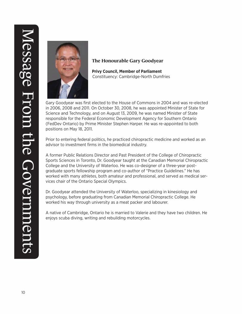
The Honourable Gary Goodyear
Privy Council, Member of Parliament
Constituency: Cambridge-North Dumfries
Gary Goodyear was fi rst elected to the House of Commons in 2004 and was re-elected in 2006, 2008 and 2011. On October 30, 2008, he was appointed Minister of State for Science and Technology, and on August 13, 2009, he was named Minister of State responsible for the Federal Economic Development Agency for Southern Ontario (FedDev Ontario) by Prime Minister Stephen Harper. He was re-appointed to both positions on May 18, 2011.
Prior to entering federal politics, he practiced chiropractic medicine and worked as an advisor to investment fi rms in the biomedical industry.
A former Public Relations Director and Past President of the College of Chiropractic Sports Sciences in Toronto, Dr. Goodyear taught at the Canadian Memorial Chiropractic College and the University of Waterloo. He was co-designer of a three-year post-graduate sports fellowship program and co-author of “Practice Guidelines.” He has worked with many athletes, both amateur and professional, and served as medical ser-vices chair of the Ontario Special Olympics.
Dr. Goodyear attended the University of Waterloo, specializing in kinesiology and psychology, before graduating from Canadian Memorial Chiropractic College. He worked his way through university as a meat packer and labourer.
A native of Cambridge, Ontario he is married to Valerie and they have two children. He enjoys scuba diving, writing and rebuilding motorcycles.
Message From
the Governm
ents
11
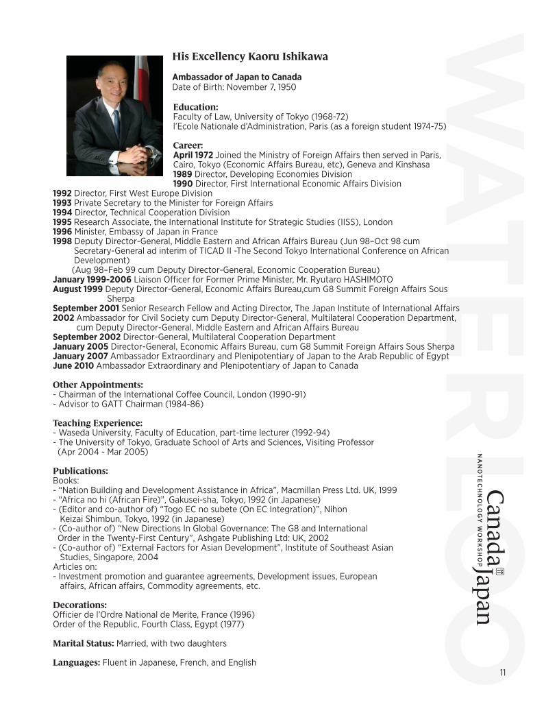
His Excellency Kaoru Ishikawa
Ambassador of Japan to Canada
Date of Birth: November 7, 1950
Education:Faculty of Law, University of Tokyo (1968-72) l’Ecole Nationale d’Administration, Paris (as a foreign student 1974-75)
Career:April 1972 Joined the Ministry of Foreign Aff airs then served in Paris, Cairo, Tokyo (Economic Aff airs Bureau, etc), Geneva and Kinshasa1989 Director, Developing Economies Division1990 Director, First International Economic Aff airs Division
1992 Director, First West Europe Division1993 Private Secretary to the Minister for Foreign Aff airs1994 Director, Technical Cooperation Division1995 Research Associate, the International Institute for Strategic Studies (IISS), London1996 Minister, Embassy of Japan in France1998 Deputy Director-General, Middle Eastern and African Aff airs Bureau (Jun 98–Oct 98 cum Secretary-General ad interim of TICAD II -The Second Tokyo International Conference on African Development) (Aug 98–Feb 99 cum Deputy Director-General, Economic Cooperation Bureau)January 1999-2006 Liaison Offi cer for Former Prime Minister, Mr. Ryutaro HASHIMOTOAugust 1999 Deputy Director-General, Economic Aff airs Bureau,cum G8 Summit Foreign Aff airs Sous SherpaSeptember 2001 Senior Research Fellow and Acting Director, The Japan Institute of International Aff airs2002 Ambassador for Civil Society cum Deputy Director-General, Multilateral Cooperation Department, cum Deputy Director-General, Middle Eastern and African Aff airs BureauSeptember 2002 Director-General, Multilateral Cooperation DepartmentJanuary 2005 Director-General, Economic Aff airs Bureau, cum G8 Summit Foreign Aff airs Sous SherpaJanuary 2007 Ambassador Extraordinary and Plenipotentiary of Japan to the Arab Republic of EgyptJune 2010 Ambassador Extraordinary and Plenipotentiary of Japan to Canada
Other Appointments:- Chairman of the International Coff ee Council, London (1990-91)- Advisor to GATT Chairman (1984-86)
Teaching Experience:- Waseda University, Faculty of Education, part-time lecturer (1992-94)- The University of Tokyo, Graduate School of Arts and Sciences, Visiting Professor (Apr 2004 - Mar 2005)
Publications:Books:- “Nation Building and Development Assistance in Africa”, Macmillan Press Ltd. UK, 1999- “Africa no hi (African Fire)”, Gakusei-sha, Tokyo, 1992 (in Japanese)- (Editor and co-author of) “Togo EC no subete (On EC Integration)”, Nihon Keizai Shimbun, Tokyo, 1992 (in Japanese)- (Co-author of) “New Directions In Global Governance: The G8 and International Order in the Twenty-First Century”, Ashgate Publishing Ltd: UK, 2002- (Co-author of) “External Factors for Asian Development”, Institute of Southeast Asian Studies, Singapore, 2004Articles on:- Investment promotion and guarantee agreements, Development issues, European aff airs, African aff airs, Commodity agreements, etc.
Decorations: Offi cier de l’Ordre National de Merite, France (1996)Order of the Republic, Fourth Class, Egypt (1977)
Marital Status: Married, with two daughters
Languages: Fluent in Japanese, French, and English
12
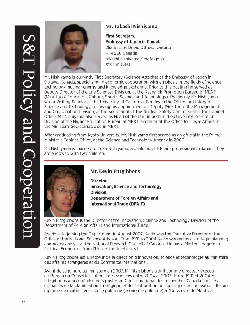
Mr. Nishiyama is currently First Secretary (Science Attaché) at the Embassy of Japan in Ottawa, Canada, specializing in economic cooperation with emphasis in the fi elds of science, technology, nuclear energy and knowledge exchange. Prior to this posting he served as Deputy Director of the Life Sciences Division, at the Research Promotion Bureau of MEXT (Ministry of Education, Culture, Sports, Science and Technology). Previously Mr. Nishiyama was a Visiting Scholar at the University of California, Berkley in the Offi ce for History of Science and Technology, following his appointment as Deputy Director of the Management and Coordination Division, at the Secretariat of the Nuclear Safety Commission in the Cabinet Offi ce. Mr. Nishiyama also served as Head of the Unit in both in the University Promotion Division of the Higher Education Bureau at MEXT, and later at the Offi ce for Legal Aff airs in the Minister’s Secretariat, also in MEXT.
After graduating from Kyoto University, Mr. Nishiyama fi rst served as an offi cial in the Prime Minister’s Cabinet Offi ce, at the Science and Technology Agency in 2000.
Mr. Nishiyama is married to Yoko Nishiyama, a qualifi ed child-care professional in Japan. They are endowed with two children.
Mr. Takashi Nishiyama
First Secretary,
Embassy of Japan in Canada
255 Sussex Drive, Ottawa, Ontario K1N 9E6 [email protected] 613-241-8451
Kevin Fitzgibbons is the Director of the Innovation, Science and Technology Division of the Department of Foreign Aff airs and International Trade.
Previous to joining the Department in August 2007, Kevin was the Executive Director of the Offi ce of the National Science Advisor. From 1991 to 2004 Kevin worked as a strategic planning and policy analyst at the National Research Council of Canada. He has a Master’s degree in Political Economics from l’Université de Montréal.
Kevin Fitzgibbons est Directeur de la direction d’innovation, science et technologie au Ministère des aff aires étrangères et du Commerce international.
Avant de se joindre au ministère en 2007, M. Fitzgibbons a agit comme directeur exécutif du Bureau du Conseiller national des sciences entre 2004 et 2007. Entre 1991 et 2004 M. Fitzgibbons a occupé plusieurs postes au Conseil national des recherches Canada dans les domaines de la planifi cation stratégique et de l’élaboration des politiques en innovation. Il a un diplôme de maitrise en science politique (économie politique) à l’Université de Montréal.
Mr. Kevin Fitzgibbons
Director,
Innovation, Science and Technology
Division,
Department of Foreign Aff airs and
International Trade (DFAIT)
S&T Policy and Cooperation

13
Mr. Yasuyoshi Kakita
Director, Generic Research and Research Plat-
form Division,
Research Promotion Bureau,
Ministry of Education, Culture, Sports,
Science and Technology (MEXT)
Government of Japan
Currier2011 -
Director, Generic Research and Research Platform Div., MEXT
2008 - 2011
Director, Planning Div., S&T Policy Bureau, MEXTCouncilor, S&T Basic Policy, Council for Science and Technology Policy (CSTP),Cabinet Offi ce(Establishment of the 4th S&T Basic Plan)
2006 - 2007
Secretary to the Minister of Science, Technology and Innovation,Cabinet Offi ce
2004 - 2005
Deputy Director, Policy Div., S&T Policy Bureau, MEXT
2001 - 2004
First Secretary (S&T), Embassy of Japan in Canada
1998 - 1999
Visiting Scholar, School of International & Public Aff airs,Columbia University
1995 - 1996
Chief, Planning Div., R&D Bureau, STA
1993 - 1995
Chief, Space Development Div., R&D Bureau, STA
1990
Offi cial, Science and Technology Agency (STA)
EducationBachelor of Engineering, Hokkaido University
S&T Policy and Cooperation

14
Mr. Richard Brommeland
Director,
Business Development & External Relations
National Institute for Nanotechnology (NINT)
Mr. Brommeland is the Director of Business Development and External Relations for Canada’s National Institute for Nanotechnology, NINT, in Edmonton. His responsibilities are to encourage collaborations which assist companies to develop or adopt nanotechnology; manage large collaborative projects; facilitate relationships with key Alberta partners and stakeholders, and with other nanotechnology R&D organizations globally; manage the NINT Innovation Center; manage intellectual property arising from NINT activities. Rick has a shared responsibility for building new ventures and strategic relationships for the Institute and for promoting its awareness in the community.
Mr. Brommeland joined NINT in 2003 following a 20 year management consulting career in the Canadian private sector, specializing in technology commercialization and new company start-ups. In the early years of his career, Rick was an engineer in the Canadian space industry, on projects ranging from rocket payload design to satellite attitude control. He later served as a new product development
engineer, and project engineer in the petroleum industry.
Dr. Kiyoshi Yase
Director,
Nanosystem research Institute (NRI),
National Institute of Advanced Industrial
Science and Technology (AIST)
Tsukuba Central 5-1, 1-1-1 Higashi, Tsukuba, Ibaraki 305-8565, JapanTEL: +81-29-861-9401, FAX: +81-29-861-6306, E-MAIL: [email protected]
Education1978-1983 B.Sc. in Polymer Science (Osaka University)1978-1980 M.Sc. in Physical and Inorganic Chemistry (Osaka University)1980-1983 D.Sc. in Crystal Chemistry (Kyoto University)Year of Dr. degree: 1986Title of the Thesis“A Study of Structure and Lattice Disordering in Molecular Thin Films by High Resolution Transmission Electron Microscopy.”
Professional ExperienceSept. 15, 1984 - July 31, 1991
Research Assistant in Faculty of Applied Biological Science, Hiroshima UniversityAug. 1, 1991 - Mar. 31, 1992
Associate Professor in Faculty of Applied Biological Science, Hiroshima UniversityApr. 1, 1992 - Dec. 31, 1992
Senior Researcher in Department of Material Engineering, Research Institute of Polymer and Textile (RIPT), Agency of Industrial Science and Technology (AIST)Jan. 1, 1993 - Mar. 31, 1994
Senior Researcher in Department of Polymer Physics, National Institute of Materials and Chemical Research (NIMC), AISTApr. 1, 1994 - Mar. 31, 1994 Laboratory Leader in Polymer Structure Lab., NIMCApr. 1, 2001 – Mar. 31, 2010
Deputy Director of Photonics Research Institute (PRI), National Institute of Advanced Industrial Science and Technology (AIST)Apr. 1, 2010 -
Director of Nanosystem Research Institute, National Institute of Advanced Industrial Science and Technology (AIST)
Building Partnerships
15
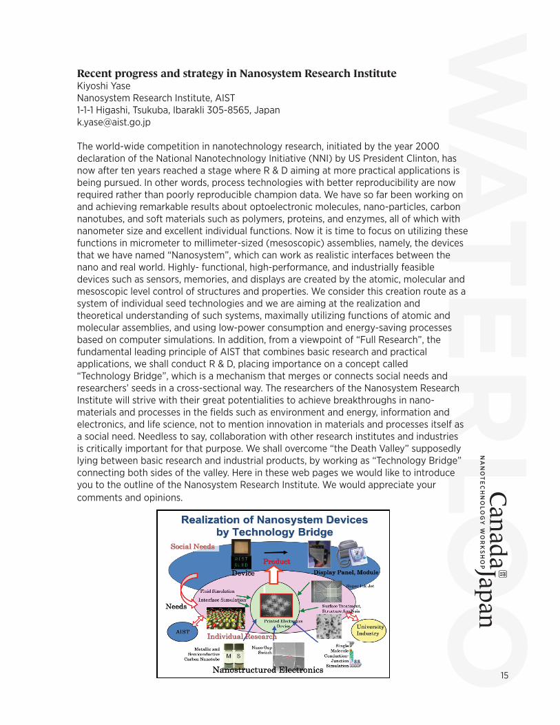
Recent progress and strategy in Nanosystem Research InstituteKiyoshi YaseNanosystem Research Institute, AIST1-1-1 Higashi, Tsukuba, Ibarakli 305-8565, [email protected]
The world-wide competition in nanotechnology research, initiated by the year 2000 declaration of the National Nanotechnology Initiative (NNI) by US President Clinton, has now after ten years reached a stage where R & D aiming at more practical applications is being pursued. In other words, process technologies with better reproducibility are now required rather than poorly reproducible champion data. We have so far been working on and achieving remarkable results about optoelectronic molecules, nano-particles, carbon nanotubes, and soft materials such as polymers, proteins, and enzymes, all of which with nanometer size and excellent individual functions. Now it is time to focus on utilizing these functions in micrometer to millimeter-sized (mesoscopic) assemblies, namely, the devices that we have named “Nanosystem”, which can work as realistic interfaces between the nano and real world. Highly- functional, high-performance, and industrially feasible devices such as sensors, memories, and displays are created by the atomic, molecular and mesoscopic level control of structures and properties. We consider this creation route as a system of individual seed technologies and we are aiming at the realization and theoretical understanding of such systems, maximally utilizing functions of atomic and molecular assemblies, and using low-power consumption and energy-saving processes based on computer simulations. In addition, from a viewpoint of “Full Research”, the fundamental leading principle of AIST that combines basic research and practical applications, we shall conduct R & D, placing importance on a concept called “Technology Bridge”, which is a mechanism that merges or connects social needs and researchers’ seeds in a cross-sectional way. The researchers of the Nanosystem Research Institute will strive with their great potentialities to achieve breakthroughs in nano-materials and processes in the fi elds such as environment and energy, information and electronics, and life science, not to mention innovation in materials and processes itself as a social need. Needless to say, collaboration with other research institutes and industries is critically important for that purpose. We shall overcome “the Death Valley” supposedly lying between basic research and industrial products, by working as “Technology Bridge” connecting both sides of the valley. Here in these web pages we would like to introduce you to the outline of the Nanosystem Research Institute. We would appreciate your comments and opinions.
16
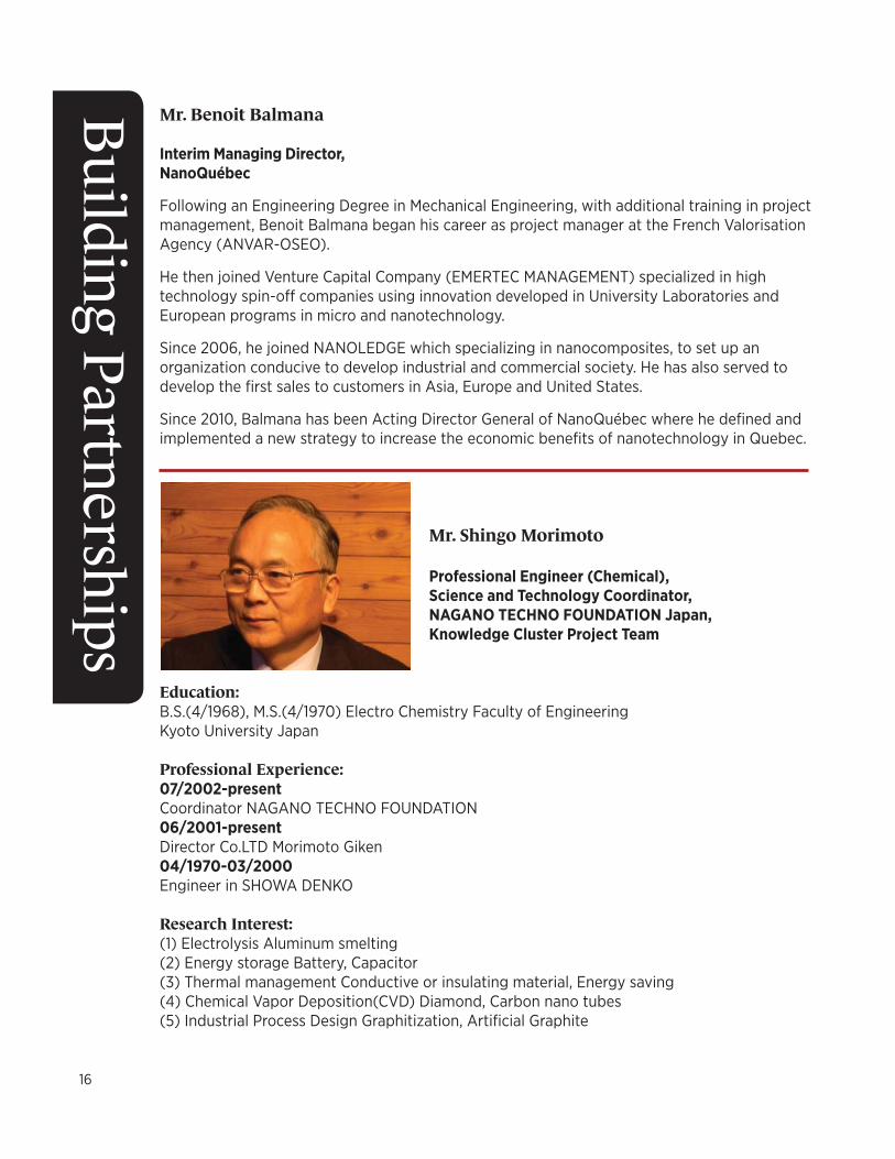
Mr. Benoit Balmana
Interim Managing Director,
NanoQuébec
Following an Engineering Degree in Mechanical Engineering, with additional training in project management, Benoit Balmana began his career as project manager at the French Valorisation Agency (ANVAR-OSEO).
He then joined Venture Capital Company (EMERTEC MANAGEMENT) specialized in high technology spin-off companies using innovation developed in University Laboratories and European programs in micro and nanotechnology.
Since 2006, he joined NANOLEDGE which specializing in nanocomposites, to set up an organization conducive to develop industrial and commercial society. He has also served to develop the fi rst sales to customers in Asia, Europe and United States.
Since 2010, Balmana has been Acting Director General of NanoQuébec where he defi ned and implemented a new strategy to increase the economic benefi ts of nanotechnology in Quebec.
Mr. Shingo Morimoto
Professional Engineer (Chemical),
Science and Technology Coordinator,
NAGANO TECHNO FOUNDATION Japan,
Knowledge Cluster Project Team
Education:B.S.(4/1968), M.S.(4/1970) Electro Chemistry Faculty of EngineeringKyoto University Japan
Professional Experience:07/2002-present
Coordinator NAGANO TECHNO FOUNDATION06/2001-present
Director Co.LTD Morimoto Giken04/1970-03/2000
Engineer in SHOWA DENKO
Research Interest:(1) Electrolysis Aluminum smelting(2) Energy storage Battery, Capacitor(3) Thermal management Conductive or insulating material, Energy saving(4) Chemical Vapor Deposition(CVD) Diamond, Carbon nano tubes(5) Industrial Process Design Graphitization, Artifi cial Graphite
Building Partnerships

17
Carbon Nanotubes Characterization and ApplicationShingo Morimoto,Nagano Techno Foundation
Carbon nanotubes were found in 1976 by Endo as extreamly thinner carbon fi bers and mass productive process of thicker nanotubes (VGCF) was developed by SHOWA DENKO. Industrial application of this material was vigorously investigated, after several years later VGCF was tested as the additives for battery. By addition them to negative electrodes, performance of LIB was extraordinarily improved. In these ten years nano materials were much interested all over the world, and carbon nanotubes are recognized as the most promising materials in nano materials because of their shape and high electro, thermal conductivities. We are pursuing to detect new and useful properties of carbn nanotubes through using newest equipment, and eveloping new applications based on new properties.
Our research
a. To observe and characterize newly developed nanocarbonsb. To develop new composites with plastics, metal, elastomers and ceramicsc. To develop newly structure controlled nanocarbon for energy devicesd. To develop new surface treating method by electro platinge. To develop newly structured nanocarbon for orthopedic surgeryf. To develop newly arranged carbon structure
18
Dr. Daisuke Fujita
Birth in 1960.12.15 (Age: 50)
Director, Advanced Key Technologies Division,
National Institute for Materials Science (NIMS)
ADDRESS: 1-2-1 Sengen, Tsukuba 305-0047, JAPANTel: +81-29-859-2741 Fax: +81-29-859-2801,E-mail: [email protected]
DIPLOMA:Graduate of the University of Tokyo (1984).Master in Materials Science (1986), the University of Tokyo.Ph.D in Materials Science (1991), the University of Tokyo.
RUN:Since 2011: Director, Advanced Key Technologies Division, NIMSSince 2011: Managing Director, Nano Characterization Unit, NIMS2010-2011: Coordinating Director, Key Nanotechnologies Field, NIMS2007-2011: Principal Investigator, WPI-Center for Materials Nanoarchitectonics, NIMS2006-2011: Managing Director, Advanced Nano Characterization Center, NIMS2004-2006: Associate Director, Extreme Field Nano Functionality Group, NIMS2001-2004: Project Leader, Active Nano-Characterization and Technology Project, Special Coordination Funds, MEXT, Japan (2001-2004)2001-2002: Leader, 6th Nanophysics Research Group, Nanomaterials Laboratory, NIMS1999-2001: Unit Leader, Extreme High Vacuum Research Station, National Research Institute for Metals (NRIM)1994-1999: Senior Research, Surface Interface Analysis Division, NRIM1991-1994: Researcher, Surface Interface Analysis Division, NRIM1986-1991: Research Associate, Institute of Industrial Science, the University of Tokyo
SPECIALITIES:Dr. Fujita’s research fi elds are nanometer-scale materials science on metals, semiconductors, superconductors, nanoclusters, and molecules in extreme environments such as low-temperature, high-magnetic fi eld and ultra-high vacuum. Novel quantum phenomena and functionality of artifi cial nanostructures observable at extreme fi elds are his research targets. Development of novel nanostructured materials such as size-controlled nanoclusters, nanowires, nanotubes is also his research interests. Major investigation tools of the researche are various scanning probe microscopes (SPM), such as scanning tunneling microscopy (STM), scanning tunneling spectroscopy (STS), STM-induced light emission (STM-LE), noncontact atomic force microscopy (NC-AFM), Kelvin Force Microscopy (KFM) and conductive AFM. Besides, various surface analysis equipments such as Low-energy Electron Diff raction (LEED), Auger Electron Spectroscopy (AES), and X-ray Photoelectron Spectroscopy (XPS) are the major analytical tools for surface nanocharacterization research.
PRIZES:2009: Ichimura Award, New Technology Development Foundation, Japan1998: Murakami Award for ‘Young Best Researcher’ of Murakami Foundation.1993: Prize for ‘Best Young Researcher of Materials Chemistry’, Japan Institute for Metals.1993: Prize for ‘Best Scientifi c Paper of Materials Chemistry’, Japan Institute of Metals..1993: Prize for ‘Best Scientifi c Paper by Young Researcher’, Surface Science Society of Japan.
PUBLICATIONS:More than 200 publications in scientifi c journals such as Nature Physics, PNAS, PRL, Nano Letters, ACS Nano, Small, Applied Physics Letters, Nanotechnology, PRB, and so on.
19
Novel Synthesis and Nanocharacterization of Graphene and h-BNDaisuke FujitaAdvanced Key Technologies Division, National Institute for Materials Science (NIMS)1-2-1 Sengen, Tsukuba 305-0047, JapanE-mail: [email protected]
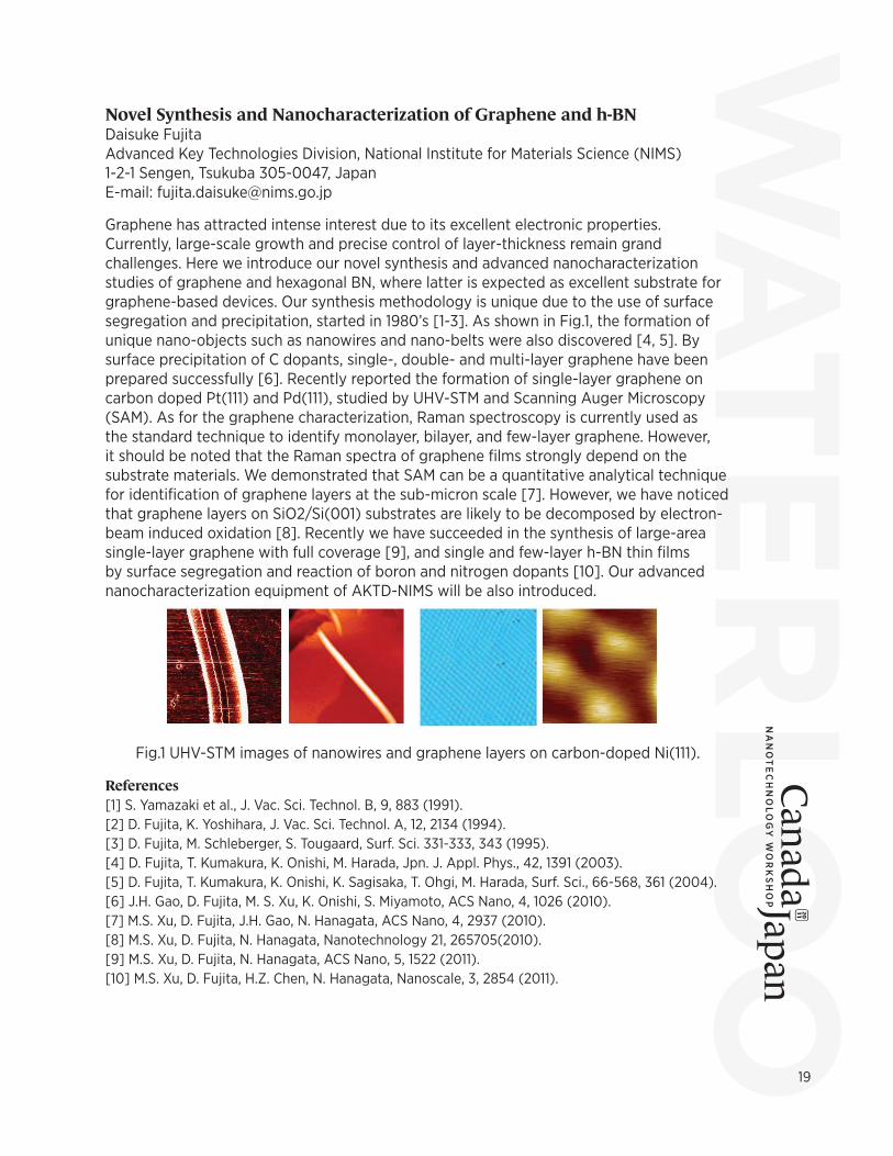
Graphene has attracted intense interest due to its excellent electronic properties. Currently, large-scale growth and precise control of layer-thickness remain grand challenges. Here we introduce our novel synthesis and advanced nanocharacterization studies of graphene and hexagonal BN, where latter is expected as excellent substrate for graphene-based devices. Our synthesis methodology is unique due to the use of surface segregation and precipitation, started in 1980’s [1-3]. As shown in Fig.1, the formation of unique nano-objects such as nanowires and nano-belts were also discovered [4, 5]. By surface precipitation of C dopants, single-, double- and multi-layer graphene have been prepared successfully [6]. Recently reported the formation of single-layer graphene on carbon doped Pt(111) and Pd(111), studied by UHV-STM and Scanning Auger Microscopy (SAM). As for the graphene characterization, Raman spectroscopy is currently used as the standard technique to identify monolayer, bilayer, and few-layer graphene. However, it should be noted that the Raman spectra of graphene fi lms strongly depend on the substrate materials. We demonstrated that SAM can be a quantitative analytical technique for identifi cation of graphene layers at the sub-micron scale [7]. However, we have noticed that graphene layers on SiO2/Si(001) substrates are likely to be decomposed by electron-beam induced oxidation [8]. Recently we have succeeded in the synthesis of large-area single-layer graphene with full coverage [9], and single and few-layer h-BN thin fi lms by surface segregation and reaction of boron and nitrogen dopants [10]. Our advanced nanocharacterization equipment of AKTD-NIMS will be also introduced.
Fig.1 UHV-STM images of nanowires and graphene layers on carbon-doped Ni(111).
References[1] S. Yamazaki et al., J. Vac. Sci. Technol. B, 9, 883 (1991).[2] D. Fujita, K. Yoshihara, J. Vac. Sci. Technol. A, 12, 2134 (1994).[3] D. Fujita, M. Schleberger, S. Tougaard, Surf. Sci. 331-333, 343 (1995).[4] D. Fujita, T. Kumakura, K. Onishi, M. Harada, Jpn. J. Appl. Phys., 42, 1391 (2003).[5] D. Fujita, T. Kumakura, K. Onishi, K. Sagisaka, T. Ohgi, M. Harada, Surf. Sci., 66-568, 361 (2004).[6] J.H. Gao, D. Fujita, M. S. Xu, K. Onishi, S. Miyamoto, ACS Nano, 4, 1026 (2010).[7] M.S. Xu, D. Fujita, J.H. Gao, N. Hanagata, ACS Nano, 4, 2937 (2010).[8] M.S. Xu, D. Fujita, N. Hanagata, Nanotechnology 21, 265705(2010).[9] M.S. Xu, D. Fujita, N. Hanagata, ACS Nano, 5, 1522 (2011).[10] M.S. Xu, D. Fujita, H.Z. Chen, N. Hanagata, Nanoscale, 3, 2854 (2011).

20
Dr. Rima Rozen
Associate Vice-Principal,
Research and International Relations,
McGill University
Dr. Rozen received her Ph.D from McGill University and pursued postdoctoral training at McGill and Yale Universities. In 1984, she became an Assistant Professor at McGill in the Departments of Human Genetics and Pediatrics, and Associate Member of the Biology Department. In 1985, Dr. Rozen established and became Director of the Molecular Genetics Diagnosis Service at the McGill-Montreal Children’s Hospital, the fi rst accredited molecular diagnosis laboratory in Quebec. She became a Fellow of the Canadian College of Medical Genetics, certifi ed in Molecular Genetics, and continued to direct the Diagnosis Service until 2002. In 1998, Dr. Rozen was appointed Professor of Human Genetics and Pediatrics. From 1999 – 2007, Dr. Rozen served as Scientifi c Director of the Montreal Children’s Hospital and Deputy Scientifi c Director of the McGill University Health Centre, until her appointment as Associate Vice-Principal (Research and International Relations) in February 2007.
Dr. Rozen’s research interests focus on the genetics of metabolic disorders and complex traits, and on genetic-nutritional interactions in disease. She has published 200 papers and supervised more than 60 graduate and undergraduate trainees. She holds 8 patents and is the scientifi c founder of a McGill spin-off company. Dr. Rozen has received several awards for her research, including the Prix Léo Parizeau from ACFAS, FRSQ chercheur-boursier, CIHR Senior Scientist award and the James McGill Professorship. Dr. Rozen has been inducted into the Canadian Academy of Health Sciences and the Royal Society of Canada
Dr. Koji Ishibashi
Advanced Device Laboratory,
RIKEN Advanced Science Institute
Koji Ishibashi was born in Kyoto, Japan in 1960. He recieved his BS and PhD in electrical engineering, Osaka Univ. in Japan in 1983 and 1988. respectively. In 1988, he joined the RIKEN institute, and has been a director of the advanced device laboratory in RIKEN since 2003. He was a visiting scientist in TU Delft in 1997-1998 and a visiting professor in Lund Univ. in 2007. He is also a professor in Tokyo Institute of Technology, Chiba Univ. and Tokyo Univ. Sci. He is a member of Japan Society of Applied Physics.
21
Carbon nanotubes and semiconductor nanowires for quantum nanodevice applicationsKoji IshibashiAdvanced Device Laboratory, RIKEN Advanced Science Institute2-1, Hirosawa, Wako, Saitama 351-0198, Japan. Email: [email protected]
Abstract:In this talk, I review research activities in my group rather than talking about specifi c topics to exchange information between Japan and Canada. In my group, we are interested in quantum nanodevices such as quantum bits (qubits) and quantum THz detectors, as well as nanofabrication in a molecular scale. To make use of quantum eff ects, the smaller structures are required, so that we use carbon nanotubes and semiconductor nanowires that are self assembly formed with an extremely small diameter. We use single-wall carbon nanotubes (SWCNTs), Si/Ge nanowires and InAs naowires, depending on the type of quantum nanodevices. In this talk, we show main experimental results on these devices listed below. Part of the works is done in collaboration with NIMS and NTT basic research lab.
1) Towards spin qubit with SWCNT and Ge quantum dots
To realize the spin qubit, we have to begin with preparing a single spin in a quantum dot (QD). To do so, there are two methods. The simplest method is to prepare absolute one electron in the dot. The other method is to realize an unpaired electron in the uppermost quantum level with many electrons in the dot. The former method is conceptually simple, but is not always easy in practice. To realize the latter condition, there are requirements among energy scales with E (level spacing) much larger than electron-electron interaction energies. We demonstrate each case with the Ge QDs and SWCNT QDs where artifi cial atom behaviours are observed.
2) Towards Andreev qubit and study of transport physics with a large spin-orbit interaction in
InAs nanowires
The InAs nanowires are known to easily make Ohmic contacts with metallic contacts. We have been studying basic properties of individual InAs nanowires with superconducting contacts (SNS), which could be a basic building block of the Andreev qubit. We will show basic transport properties of the SNS structures, which includes supercurrent modulated by gate voltage, its magnetic fi eld and temperature dependence, and microwave eff ects. These results indicate the dirty Josephson junction behaviours.
3) Quantum response of the SWCNT quantum dots
One of the unique features of the SWCNT QDs is large energy scales, associated with the artifi cial atom (QD), which fall in a teraherz (THz) range. This fact made us to explore the quantum response of the SWCNT QDs to the THz wave. In fact, we have observed the THz photon assisted tunnelling in the Coulomb blockade oscillations with frequency-dependent satellite peaks.
4) SWCNT/Molecule heterustructures for molecular scale nanostructures
Another unique feature of the SWCNT would be a possible chemical modifi cation of the nanotube ends and a surface. This makes it possible to fabricate chemically bonded SWCNT/molecule heterojunctions. As examples, we show chemically bonded individual SWCNT rings and SWCNT/molecule heterostructures to fabricate a QD. The structures are characterized by a scanning tunnelling microscope with simultaneous optical spectroscopy, such as Raman and photo-current spectroscopy and the electric fi eld modulation spectroscopy.
References[1]. S. Moriyama, T. Fuse, M. Suzuki, Y. Aoyagi, K. Ishibashi, Phys. Rev. Lett. 94, 186806 (2005)[2]. T. Nishio, T. Kozakai, S. Amaha, M. Larsson, H. Nilsson, H. Q. Xu, G. Q. Zhang, K. Tateno, H. Takayanagi and K. Ishibashi, Nanotechnology, 44, 5701 (2011)[3]. Y. Kawano, T. Fuse, S. Toyokawa, T. Uchida, K. Ishibashi, J. Appl. Phys. 103, 034307 (2008)

22
Mr. Dan Djukich
Director, NanoAlberta
Dan is presently the Director of NanoAlberta at Alberta Innovates – Technology Futures. Dan is responsible for the implementation of the industrial-focused Alberta Nanotechnology Strategy. Dan was part of the team at the Alberta Ministry of Advanced Education and Technology (AET) that formed nanoAlberta back in July 2008. Prior to that, Dan spent 5 years as the Manager of Electronics, Microsystems and Nanotechnology in the Technology Commercialization Division within AET and was the internal champion, establishing ACAMP (Alberta Centre for Advanced MNT Products) as a key element of the Alberta Nanotechnology Strategy.
Dan was previously, CoFounder and Director of Sales for ZiMARC, a former division of Alberta Research Council. Dan also has extensive industrial experience working in sales and operations with ThermicEdge, WESTAIM and LSI Logic and holds a BSc. degree from the University of Alberta
Ms. Jenny Reilly
Director, Canada-Japan Co-op Program,
The Canada-Japan Co-op Program,
The University of British Columbia
2385 East Mall, Vancouver, British ColumbiaCanada V6T1Z4Phone: 604-822-6598Fax: [email protected]
The Canada-Japan Co-op Program is a Canadian university/college based, international co-op/internship program linking engineering, science, business and arts undergraduate students from across Canada with highly committed Japanese businesses.
The Canada-Japan Co-op Program (CJCP) is a self-funded, national consortium model providing co-op opportunities in Japan to member institutions from across the country. In 2011 the program celebrates its 20 year anniversary and has placed over 800 co-op students in 4, 8 or 12-month, paid co-op work terms in Japan to date. The Program has been hosted at the University of British Columbia for the past six years and prior to that time was housed at The University of Victoria. There are currently 15 Canadian Universities/Institutes participating in the program and to date in the 2011/2012 fi scal year, 42 student placements have been secured.
Educational Panel
23
Dr. Christopher Barrett
Associate Professor,
Department of Chemistry,
Exploring Physical Polymer Chemistry and Thin Film Optics,
McGill
[email protected]/main.htm
Research AreasThe approach to research taken by the Barrett Group is to apply, for the fi rst time, the emerging fi eld of photonics to the new technique of self-assembly of multi-layer thin fi lms, built from dilute solution. This novel approach to photonic devices will concentrate on the communication between light signals, and the bulk and surface structure of the fi lms. Specifi cally, this program of research is an investigation of the optical and surface properties of thin fi lms of novel polymers. The optical and surface properties are interrelated in these materials, allowing studies both of how light can be used to gather information about surfaces and structures, and how light can be used to infl uence surface and structural properties. This will be accomplished with polymer materials which incorporate both light-absorbing photo-active groups (azobenzene chromophores), and water-soluble ionic groups (electrolytes).
Educational BackgroundB.Sc. (Queen’s University, 1992)Ph.D. (Queen’s University, 1997)NSERC Postdoctoral Fellow (MIT, 1998-1999)JSPS Visiting Professor (Tokyo Tech., 2006-2007)
LeadershipConvener of Graduate Materials Program, Faculty of ScienceDirector of Undergraduate Studies, Faculty of Science
MemberCentre for Self-Assembled Chemical StructuresMcGill Institute for Advanced MaterialsMcGill Centre for the Physics of MaterialsCanadian Institute for Neutron Scattering
Azo Polymers for Sunlight-Driven Robotics: a McGill-RIKEN Collaboration.Christopher Barrett. McGill Chemistry, RIKEN, Tokyo Tech.
Polymers based on azobenzene are mimics of the retinal photo-switch that enables vision, responding physically and mechanically to permit solar energy to be converted directly to mechanical work. Reversible changes in surface energy are also inducible as a result, for a variety of reversible surface energy switching applications via light. Irradiation with light in the solar spectrum at sun-like intensities has been shown to lead to a measurable reversible photo-expansion of these coatings, of up to a few %, allowing the materials to function as photo-mechanical switches or light energy harvesters and actuator devices. New azo polymers to optimize this eff ect were developed at McGill Chemistry, and some simple macroscopic devices were fabricated with them at RIKEN to that take mechanical advantage of this eff ect for larger scale motion driven by sunlight, such as bending, ‘walking’, rolling and other applications as ‘artifi cial muscles’. The mechanism for this eff ect will be discussed from studies using ellipsometry, light-bending of AFM cantilevers, surface plasmon resonance spectroscopy, and neutron refl ectometry.
24
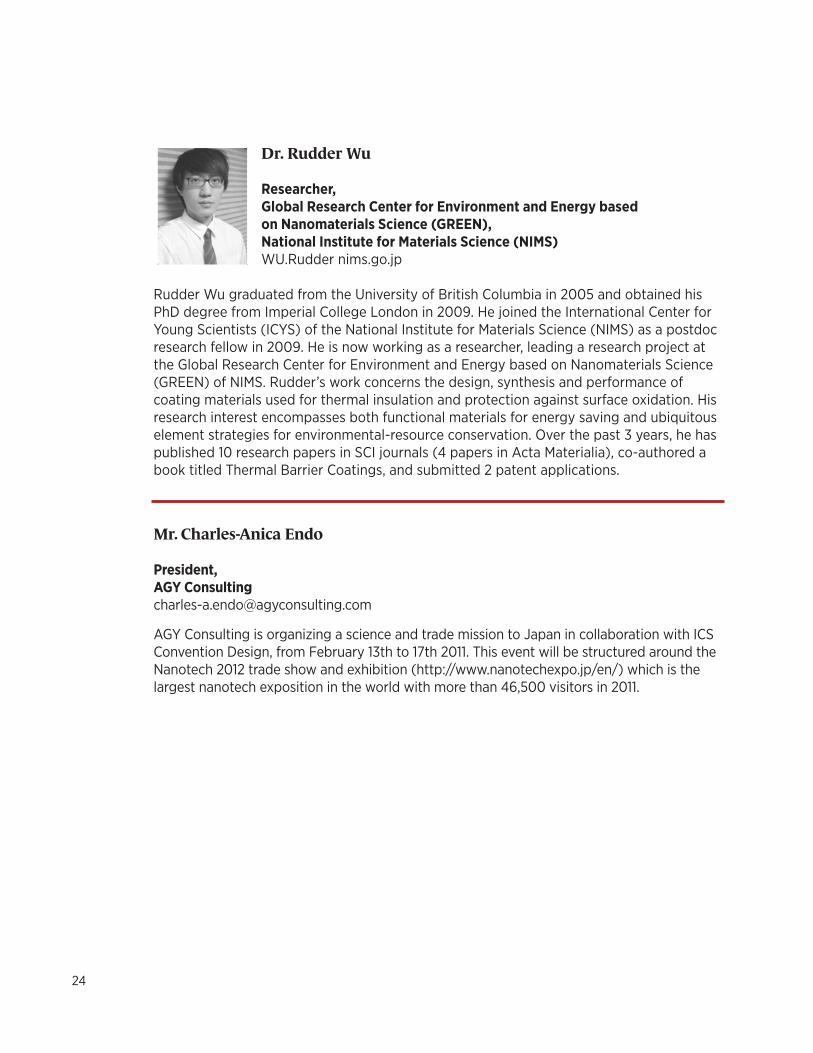
Dr. Rudder Wu
Researcher,
Global Research Center for Environment and Energy based
on Nanomaterials Science (GREEN),
National Institute for Materials Science (NIMS)
WU.Rudder nims.go.jp
Rudder Wu graduated from the University of British Columbia in 2005 and obtained his PhD degree from Imperial College London in 2009. He joined the International Center for Young Scientists (ICYS) of the National Institute for Materials Science (NIMS) as a postdoc research fellow in 2009. He is now working as a researcher, leading a research project at the Global Research Center for Environment and Energy based on Nanomaterials Science (GREEN) of NIMS. Rudder’s work concerns the design, synthesis and performance of coating materials used for thermal insulation and protection against surface oxidation. His research interest encompasses both functional materials for energy saving and ubiquitous element strategies for environmental-resource conservation. Over the past 3 years, he has published 10 research papers in SCI journals (4 papers in Acta Materialia), co-authored a book titled Thermal Barrier Coatings, and submitted 2 patent applications.
Mr. Charles-Anica Endo
President,
AGY Consulting
AGY Consulting is organizing a science and trade mission to Japan in collaboration with ICS Convention Design, from February 13th to 17th 2011. This event will be structured around the Nanotech 2012 trade show and exhibition (http://www.nanotechexpo.jp/en/) which is the largest nanotech exposition in the world with more than 46,500 visitors in 2011.
25
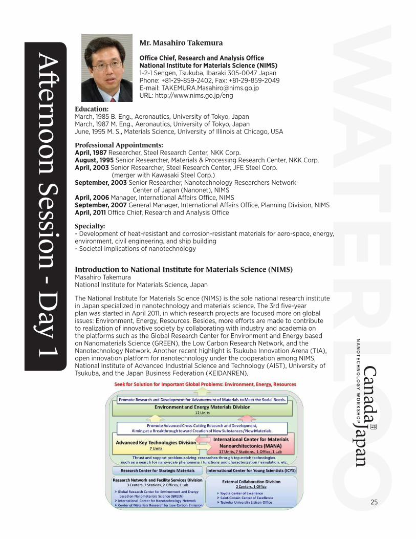
Mr. Masahiro Takemura
Offi ce Chief, Research and Analysis Offi ce
National Institute for Materials Science (NIMS)
1-2-1 Sengen, Tsukuba, Ibaraki 305-0047 JapanPhone: +81-29-859-2402, Fax: +81-29-859-2049E-mail: [email protected]: http://www.nims.go.jp/eng
Education:March, 1985 B. Eng., Aeronautics, University of Tokyo, JapanMarch, 1987 M. Eng., Aeronautics, University of Tokyo, JapanJune, 1995 M. S., Materials Science, University of Illinois at Chicago, USA
Professional Appointments:April, 1987 Researcher, Steel Research Center, NKK Corp.August, 1995 Senior Researcher, Materials & Processing Research Center, NKK Corp.April, 2003 Senior Researcher, Steel Research Center, JFE Steel Corp. (merger with Kawasaki Steel Corp.)September, 2003 Senior Researcher, Nanotechnology Researchers Network Center of Japan (Nanonet), NIMSApril, 2006 Manager, International Aff airs Offi ce, NIMSSeptember, 2007 General Manager, International Aff airs Offi ce, Planning Division, NIMSApril, 2011 Offi ce Chief, Research and Analysis Offi ce
Specialty:- Development of heat-resistant and corrosion-resistant materials for aero-space, energy, environment, civil engineering, and ship building- Societal implications of nanotechnology
Introduction to National Institute for Materials Science (NIMS)Masahiro TakemuraNational Institute for Materials Science, Japan
The National Institute for Materials Science (NIMS) is the sole national research institute in Japan specialized in nanotechnology and materials science. The 3rd fi ve-year plan was started in April 2011, in which research projects are focused more on global issues: Environment, Energy, Resources. Besides, more eff orts are made to contribute to realization of innovative society by collaborating with industry and academia on the platforms such as the Global Research Center for Environment and Energy based on Nanomaterials Science (GREEN), the Low Carbon Research Network, and the Nanotechnology Network. Another recent highlight is Tsukuba Innovation Arena (TIA), open innovation platform for nanotechnology under the cooperation among NIMS, National Institute of Advanced Industrial Science and Technology (AIST), University of Tsukuba, and the Japan Business Federation (KEIDANREN),
Aft ernoon Session - D
ay 1
26
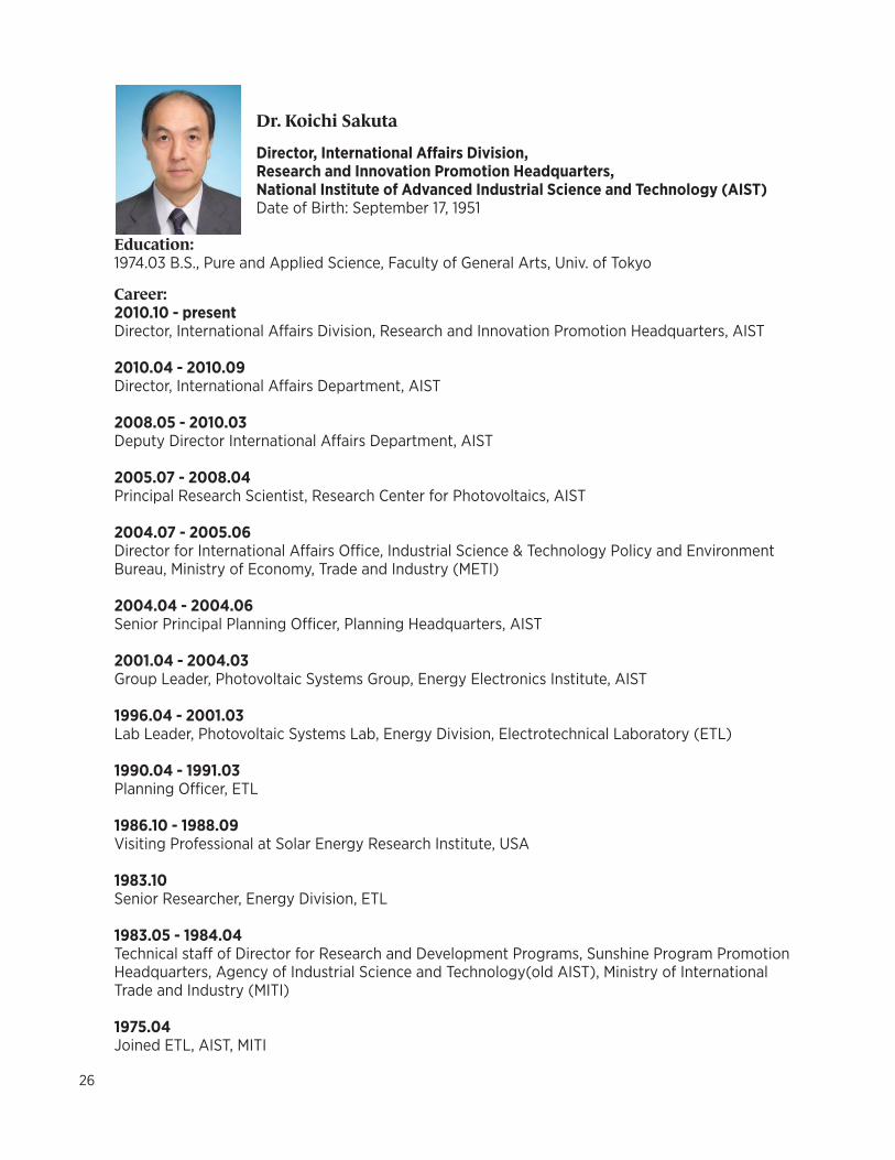
Dr. Koichi Sakuta
Director, International Aff airs Division,
Research and Innovation Promotion Headquarters,
National Institute of Advanced Industrial Science and Technology (AIST)
Date of Birth: September 17, 1951
Education:1974.03 B.S., Pure and Applied Science, Faculty of General Arts, Univ. of Tokyo
Career:2010.10 - present
Director, International Aff airs Division, Research and Innovation Promotion Headquarters, AIST
2010.04 - 2010.09
Director, International Aff airs Department, AIST
2008.05 - 2010.03
Deputy Director International Aff airs Department, AIST
2005.07 - 2008.04
Principal Research Scientist, Research Center for Photovoltaics, AIST
2004.07 - 2005.06
Director for International Aff airs Offi ce, Industrial Science & Technology Policy and Environment Bureau, Ministry of Economy, Trade and Industry (METI)
2004.04 - 2004.06
Senior Principal Planning Offi cer, Planning Headquarters, AIST
2001.04 - 2004.03
Group Leader, Photovoltaic Systems Group, Energy Electronics Institute, AIST
1996.04 - 2001.03
Lab Leader, Photovoltaic Systems Lab, Energy Division, Electrotechnical Laboratory (ETL)
1990.04 - 1991.03
Planning Offi cer, ETL
1986.10 - 1988.09
Visiting Professional at Solar Energy Research Institute, USA
1983.10
Senior Researcher, Energy Division, ETL
1983.05 - 1984.04
Technical staff of Director for Research and Development Programs, Sunshine Program Promotion Headquarters, Agency of Industrial Science and Technology(old AIST), Ministry of International Trade and Industry (MITI)
1975.04
Joined ETL, AIST, MITI
27
Overview of National Institute of Advanced Industrial Science and Technology (AIST)Koichi SakutaInternational Aff airs Division, AIST
The National Institute of Advanced Industrial Science and Technology (AIST), led by President Nomakuchi, is a public research institution funded mainly by the Japanese government. The present AIST is a rather new research organization established in 2001. However, AIST and its predecessor organizations have been contributing to society through continuous advancement in technologies and support of Japanese industries since 1882. Headquarters of AIST are located in Tsukuba and Tokyo. AIST has over 40 autonomous research units in various innovative research fi elds, and the units are located at nine research bases all over Japan. About 2400 researchers (about 2100 with tenure: about 80 from abroad) and thousands of visiting scientists, post-doctoral fellows, and students from home and abroad are working at AIST. About 700 permanent administrative personnel and many temporary staff support research works of AIST.
AIST’s research is advanced by its Research Units. They are classifi ed into three types: “Research Center” is temporary research unit which intensively conducts top-notched R&D to meet high social needs; “Research Institute” is continual and fundamental Research Unit from which novel Research Centers diverges and with which terminated Research Centers converges; “Research Laboratory” is established with swift and fl exible strategic decision and acts as a precursor to a future-Research Center. From strategic point of view, AIST continually and fl exibly reviews and reconstructs these research units.
We timely recruit excellent domestic and foreign researchers and endeavor to fi nd and to address most urged issues we face today. As the world-wide competition of innovation becomes keener, AIST’s role as a hub system of public research domain has become critically important than ever. Therefore, along with many activities promoting nation’s industrial science and technology, AIST proactively participates in “Research and Development Partnership”, aiming to accomplish its primary mission: Reinforcement of Open Innovation Hub function.
Japanese government positioned Green Innovation and Life Innovation as two important factors for progress. These two innovations are approaches for tackling urgent issues in Japanese society, such as climate change, establishing a low-carbon economy, and dealing with an aging society. To promote these innovations, AIST needs to develop open innovation. That is to say, it must respond to increasingly complex science and technology, large-scale research and development, globalization of the economic society of recent years, and promote an opportunity for a variety of members of industry, academia and government to participate actively, share the same future vision and work together with concerted eff orts.
Being one of the largest public research institutions in Japan, AIST leverages and develops its human resources in various research fi elds, advanced infrastructures in research, accumulated research fi ndings, systems for technology fusion and personnel training, and regional research bases and their networks, on the basis of social trends. Furthermore, we take a core role as an open innovation hub for industry-academia-government collaboration and cooperation with society. In other words, AIST aims to “reinforce functions of an open innovation hub” as a research and innovation promotion strategy.
28
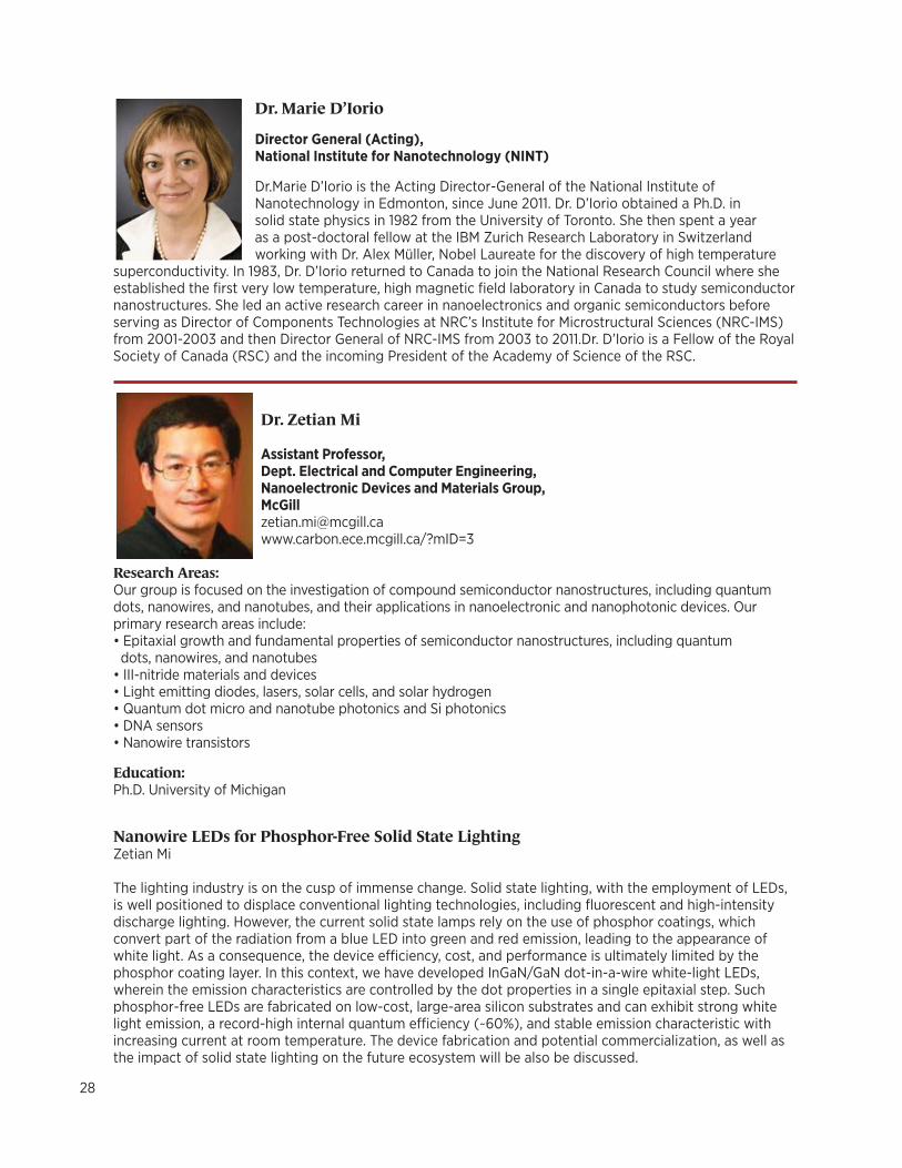
Dr. Marie D’Iorio
Director General (Acting),
National Institute for Nanotechnology (NINT)
Dr.Marie D’Iorio is the Acting Director-General of the National Institute of Nanotechnology in Edmonton, since June 2011. Dr. D’Iorio obtained a Ph.D. in solid state physics in 1982 from the University of Toronto. She then spent a year as a post-doctoral fellow at the IBM Zurich Research Laboratory in Switzerland working with Dr. Alex Müller, Nobel Laureate for the discovery of high temperature
superconductivity. In 1983, Dr. D’Iorio returned to Canada to join the National Research Council where she established the fi rst very low temperature, high magnetic fi eld laboratory in Canada to study semiconductor nanostructures. She led an active research career in nanoelectronics and organic semiconductors before serving as Director of Components Technologies at NRC’s Institute for Microstructural Sciences (NRC-IMS) from 2001-2003 and then Director General of NRC-IMS from 2003 to 2011.Dr. D’Iorio is a Fellow of the Royal Society of Canada (RSC) and the incoming President of the Academy of Science of the RSC.
Dr. Zetian Mi
Assistant Professor,
Dept. Electrical and Computer Engineering,
Nanoelectronic Devices and Materials Group,
McGill
[email protected]/?mID=3
Research Areas: Our group is focused on the investigation of compound semiconductor nanostructures, including quantum dots, nanowires, and nanotubes, and their applications in nanoelectronic and nanophotonic devices. Our primary research areas include:• Epitaxial growth and fundamental properties of semiconductor nanostructures, including quantum dots, nanowires, and nanotubes• III-nitride materials and devices• Light emitting diodes, lasers, solar cells, and solar hydrogen• Quantum dot micro and nanotube photonics and Si photonics• DNA sensors• Nanowire transistors
Education:Ph.D. University of Michigan
Nanowire LEDs for Phosphor-Free Solid State LightingZetian Mi
The lighting industry is on the cusp of immense change. Solid state lighting, with the employment of LEDs, is well positioned to displace conventional lighting technologies, including fl uorescent and high-intensity discharge lighting. However, the current solid state lamps rely on the use of phosphor coatings, which convert part of the radiation from a blue LED into green and red emission, leading to the appearance of white light. As a consequence, the device effi ciency, cost, and performance is ultimately limited by the phosphor coating layer. In this context, we have developed InGaN/GaN dot-in-a-wire white-light LEDs, wherein the emission characteristics are controlled by the dot properties in a single epitaxial step. Such phosphor-free LEDs are fabricated on low-cost, large-area silicon substrates and can exhibit strong white light emission, a record-high internal quantum effi ciency (~60%), and stable emission characteristic with increasing current at room temperature. The device fabrication and potential commercialization, as well as the impact of solid state lighting on the future ecosystem will be also be discussed.
29
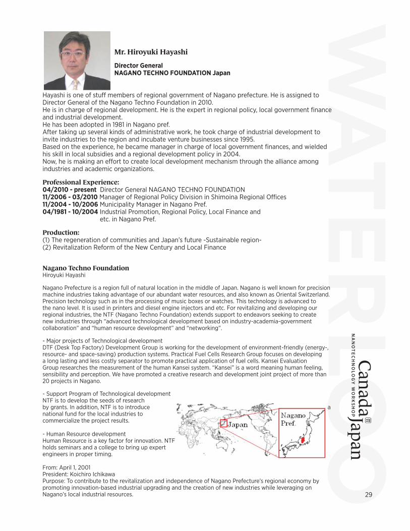
Mr. Hiroyuki Hayashi
Director General
NAGANO TECHNO FOUNDATION Japan
Hayashi is one of stuff members of regional government of Nagano prefecture. He is assigned to Director General of the Nagano Techno Foundation in 2010.He is in charge of regional development. He is the expert in regional policy, local government fi nance and industrial development.He has been adopted in 1981 in Nagano pref.After taking up several kinds of administrative work, he took charge of industrial development to invite industries to the region and incubate venture businesses since 1995.Based on the experience, he became manager in charge of local government fi nances, and wielded his skill in local subsidies and a regional development policy in 2004.Now, he is making an eff ort to create local development mechanism through the alliance among industries and academic organizations.
Professional Experience:04/2010 - present Director General NAGANO TECHNO FOUNDATION11/2006 - 03/2010 Manager of Regional Policy Division in Shimoina Regional Offi ces11/2004 - 10/2006 Municipality Manager in Nagano Pref.04/1981 - 10/2004 Industrial Promotion, Regional Policy, Local Finance and etc. in Nagano Pref.
Production:(1) The regeneration of communities and Japan’s future -Sustainable region-(2) Revitalization Reform of the New Century and Local Finance
Nagano Techno FoundationHiroyuki Hayashi
Nagano Prefecture is a region full of natural location in the middle of Japan. Nagano is well known for precision machine industries taking advantage of our abundant water resources, and also known as Oriental Switzerland. Precision technology such as in the processing of music boxes or watches. This technology is advanced to the nano level. It is used in printers and diesel engine injectors and etc. For revitalizing and developing our regional industries, the NTF (Nagano Techno Foundation) extends support to endeavors seeking to create new industries through “advanced technological development based on industry-academia-government collaboration” and “human resource development” and “networking”.
- Major projects of Technological developmentDTF (Desk Top Factory) Development Group is working for the development of environment-friendly (energy-, resource- and space-saving) production systems. Practical Fuel Cells Research Group focuses on developing a long lasting and less costly separator to promote practical application of fuel cells. Kansei Evaluation Group researches the measurement of the human Kansei system. “Kansei” is a word meaning human feeling, sensibility and perception. We have promoted a creative research and development joint project of more than 20 projects in Nagano.
- Support Program of Technological developmentNTF is to develop the seeds of research by grants. In addition, NTF is to introduce a national fund for the local industries to commercialize the project results.
- Human Resource developmentHuman Resource is a key factor for innovation. NTF holds seminars and a college to bring up expert engineers in proper timing.
From: April 1, 2001President: Koichiro IchikawaPurpose: To contribute to the revitalization and independence of Nagano Prefecture’s regional economy by promoting innovation-based industrial upgrading and the creation of new industries while leveraging on Nagano’s local industrial resources.
30
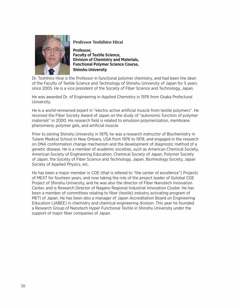
Professor Toshihiro Hirai
Professor,Faculty of Textile Science, Division of Chemistry and Materials, Functional Polymer Science Course,
Shinshu University
Dr. Toshihiro Hirai is the Professor in functional polymer chemistry, and had been the dean of the Faculty of Textile Science and Technology of Shinshu University of Japan for 5 years since 2005. He is a vice president of the Society of Fiber Science and Technology, Japan.
He was awarded Dr. of Engineering in Applied Chemistry in 1976 from Osaka Prefectural University.
He is a world-renowned expert in “electro active artifi cial muscle from textile polymers”. He received the Fiber Society Award of Japan on the study of “autonomic function of polymer materials” in 2000. His research fi eld is related to emulsion polymerization, membrane phenomena, polymer gels, and artifi cial muscle.
Prior to joining Shinshu University in 1979, he was a research instructor of Biochemistry in Tulane Medical School in New Orleans, USA from 1976 to 1978, and engaged in the research on DNA conformation change mechanism and the development of diagnostic method of a genetic disease. He is a member of academic societies, such as American Chemical Society, American Society of Engineering Education, Chemical Society of Japan, Polymer Society of Japan, the Society of Fiber Science and Technology, Japan, Biorheology Society, Japan Society of Applied Physics, etc.
He has been a major member in COE (that is refered to “the center of excellence”) Projects of MEXT for fourteen years, and now taking the role of the project leader of Golobal COE Project of Shinshu University, and he was also the director of Fiber Nanotech Innovation Center, and is Research Director of Nagano Regional Industrial Innovation Cluster. He has been a member of committees relating to fi ber (textile) industry activating program of METI of Japan. He has been also a manager of Japan Accreditation Board on Engineering Education (JABEE) in chemistry and chemical engineering division. This year he founded a Research Group of Nanotech Hyper Functional Textile in Shinshu University under the support of major fi ber companies of Japan.
31
Shinshu UniversityToshihiro Hirai
Shinshu University was established in 1949 as a national university, and became a National University Corporation on the 1st April, 2004.
Professor Morinobu Endo, Faculty of Engineering, has established the bulk synthesis of carbon nanofi bers. We has launched the ICST with a target of becoming the world-class core education and research institute of “CARBON” by combining widespread education and research resources in Shinshu University. We conduct world-class leading-edge research on carbon nanotechnology at our Carbon Science Research Center.
Faculty of Textile Science is only one in Japan. The Global Center of Excellence Program (COE) culminated in the establishment of the International Center of Excellence for Frontier Fiber-Textile science in 2007. We are educating international research specialists in cutting edge technology. We are also working on several large government projects to promote interdisciplinary cutting edge research, such as Nanotech High Function Fiber, support and assistance for young researchers through the International Young Researchers Empowerment Center and the Second Generation Intellectual Cluster program.
President: YAMASAWA KiyohitoFaculties: Arts, Education, Economics, Science, Engineering, Agriculture, Textile Science and Technology , School of MedicineFacilities for Research and Education: Shinshu Univ. International Center (SUIC), Institute of Mountain Science (IMS), Institute of Carbon Science and Technology, Cooperative Research Center, Satellite Venture Business Laboratory, Innovation Research and Support Center, Collaborative Innovation Center for Nanotech FIBER, International Young Researchers Empowerment Center, Shinshu Univ. Industrial Liaison Offi ce (SILO) and etc.Number of Staff (2010): 2,368 Academic Staff 1,150, Administrative Staff 1,218Number of Students(2010): Faculties 9,364 (Engineering2,160, Textile Science and Technology 1,270)Number of Degrees Conferred in 2009: Master’s Program 692, Doctor’s program 99, Professional Degree Course 26The International Partnership agreement Between Universities: 50 Universities (China16, Korea8, Poland3, Vietnam3, Thailand2, Indonesia2, United States3, United Kingdom1, France2, Australia2, India1, Mongolia1, Germany2, Belgium1, Russia2, Morocco1)The International Partnership agreement Between Faculties: 35 Universities (Korea9, Thailand4, Germany3, China2, United States2, United Kingdom2, Italy2, Bangladesh1, Mongolia1, Switzerland1, Taiwan1, India1, Nepal1, Australia1, Austria1, Canada3)
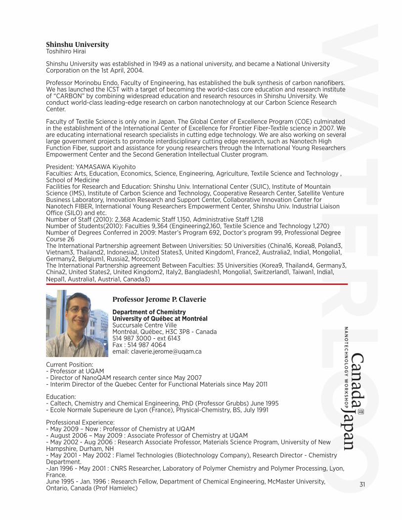
Professor Jerome P. Claverie
Department of Chemistry University of Québec at MontréalSuccursale Centre VilleMontréal, Québec, H3C 3P8 - Canada514 987 3000 - ext 6143Fax : 514 987 4064email: [email protected]
Current Position:- Professor at UQAM - Director of NanoQAM research center since May 2007- Interim Director of the Quebec Center for Functional Materials since May 2011
Education:- Caltech, Chemistry and Chemical Engineering, PhD (Professor Grubbs) June 1995- Ecole Normale Superieure de Lyon (France), Physical-Chemistry, BS, July 1991
Professional Experience:- May 2009 – Now : Professor of Chemistry at UQAM- August 2006 – May 2009 : Associate Professor of Chemistry at UQAM- May 2002 - Aug 2006 : Research Associate Professor, Materials Science Program, University of New Hampshire, Durham, NH- May 2001 - May 2002 : Flamel Technologies (Biotechnology Company), Research Director - Chemistry Department. -Jan 1996 - May 2001 : CNRS Researcher, Laboratory of Polymer Chemistry and Polymer Processing, Lyon, France. June 1995 - Jan. 1996 : Research Fellow, Department of Chemical Engineering, McMaster University, Ontario, Canada (Prof Hamielec)
32
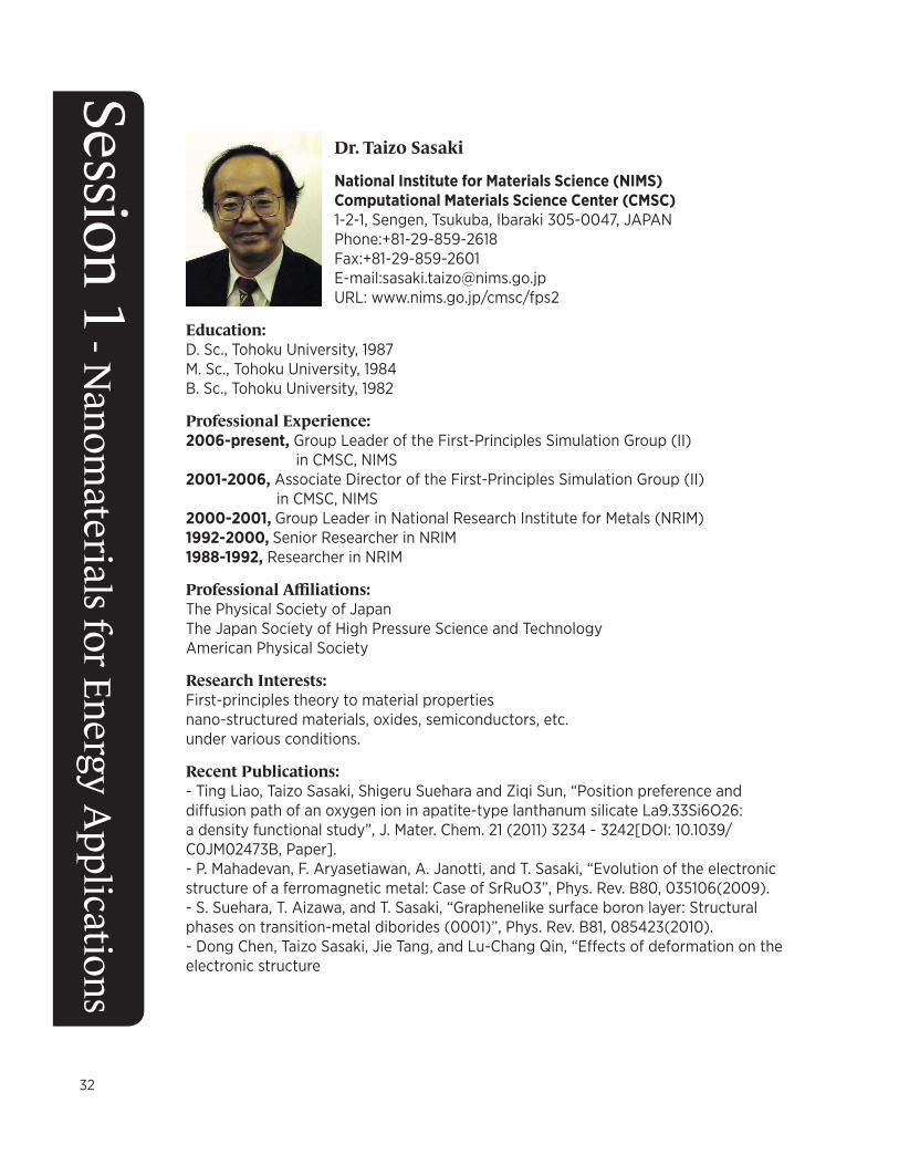
Dr. Taizo Sasaki
National Institute for Materials Science (NIMS)
Computational Materials Science Center (CMSC)
1-2-1, Sengen, Tsukuba, Ibaraki 305-0047, JAPANPhone:+81-29-859-2618Fax:+81-29-859-2601E-mail:[email protected]: www.nims.go.jp/cmsc/fps2
Education:D. Sc., Tohoku University, 1987M. Sc., Tohoku University, 1984B. Sc., Tohoku University, 1982
Professional Experience:2006-present, Group Leader of the First-Principles Simulation Group (II) in CMSC, NIMS2001-2006, Associate Director of the First-Principles Simulation Group (II) in CMSC, NIMS2000-2001, Group Leader in National Research Institute for Metals (NRIM)1992-2000, Senior Researcher in NRIM1988-1992, Researcher in NRIM
Professional Affi liations:The Physical Society of JapanThe Japan Society of High Pressure Science and TechnologyAmerican Physical Society
Research Interests:First-principles theory to material propertiesnano-structured materials, oxides, semiconductors, etc.under various conditions.
Recent Publications:- Ting Liao, Taizo Sasaki, Shigeru Suehara and Ziqi Sun, “Position preference and diff usion path of an oxygen ion in apatite-type lanthanum silicate La9.33Si6O26: a density functional study”, J. Mater. Chem. 21 (2011) 3234 - 3242[DOI: 10.1039/C0JM02473B, Paper].- P. Mahadevan, F. Aryasetiawan, A. Janotti, and T. Sasaki, “Evolution of the electronic structure of a ferromagnetic metal: Case of SrRuO3”, Phys. Rev. B80, 035106(2009).- S. Suehara, T. Aizawa, and T. Sasaki, “Graphenelike surface boron layer: Structural phases on transition-metal diborides (0001)”, Phys. Rev. B81, 085423(2010).- Dong Chen, Taizo Sasaki, Jie Tang, and Lu-Chang Qin, “Eff ects of deformation on the electronic structure
Session 1 - N
anomaterials for Energy A
pplications

33
A Theoretical Study on the Energy Materials: the Oxygen Diff usion in the La-Apatite OxideTaizo Sasaki1,Ting Liao1, Shigeru Suehara1, and Ziqi Sun21Computational Materials Science Center, NIMS,and 3WPI Intrnational Center for Materials Nanoarchitectonics, NIMS
The fuel cell is an energy devise which realizes highly-effi cient energy production. One of the major issues of the fuel cell is the operating temperature. While the solid oxide fuel cell (SOFC) is adequate for the high temperature operation achieving the very high effi ciency, oxides which can be operated in the middle temperature range (<1000C) are also desired to avoid the heat damage.
The lanthanum-silicate apatite is an ionic conductor showing the oxygen migration, and is one of the candidates to the mid.-temperature SOFC electrolyte. In spite of its high performance in the conduction property, the mechanism of the oxygen transport has not been established well yet. We have studied the behavior of the defects in La9.33Si6O26 with the fi rst-principles theory within the density-functional theory. Previous experimental studies suggested that interstitial oxygen diff uses, not oxygen vacancy. The results have shown that the excess oxygen ion forms the split interstitial pair with the original oxygen ion as the stable geometry. The migration search ended in the results (1) that the barrier height was in the observed range with the interstitialcy mechanism (Fig. 1), and (2) that the La vacancy plays an essential role in the barrier height by making the potential energy profi le bumpy. The analyses have provided the key characteristics which determine the diff usion performance.
This research was partly supported by Grant-in-Aid for Scientifi c Research (C) (No. 22560663) from Japan Society for the Promotion of Science.
Figure 1. Calculated trace of the oxygen interstitial. The interstitial oxygen diff uses by the interstitialcy mechanism, i.e. pushing out the another oxygen and r eplacing it.
34
Dr. Holger Kleinke
Professor,
Canada Research Chair,
Department of Chemistry,
Waterloo Institute for Nanotechnology,
University of Waterloo
Professor Kleinke holds a Canada Research Chair in Solid State Chemistry, and is investigating thermoelectric materials since joining the University of Waterloo in January 2000. Professor Kleinke’s international recognition is refl ected in several invited presentations at international thermoelectric conferences and numerous invitations to Canadian and international chemistry conferences. He serves as Editor for Journal of Alloys and Compounds, and is a member of the editorial boards of Chemistry of Materials and of Journal of Solid State Chemistry. Professor Kleinke received the Premier’s Research Excellence Award in 2000, and the Ontario Distinguished Researcher Award in 2002.
Nanostructuring of Thermoelectric MaterialsHolger Kleinke
With the depletion of natural resources, the exploration of the alternative energy resources is becoming more and more imperative for sustainable development. Thermoelectric materials are attracting extensive interest because of their potential of converting temperature gradients into electricity. This technology is anticipated to be used to gain electricity from the nowadays abundant waste heat, e.g. in manufacturing industries as well as in automotives, where it was shown to yield signifi cant gas economy improvements.
The use of this energy conversion today is still impeded by its low conversion effi ciency; therefore, we attempt to develop more effi cient thermoelectric materials, e.g. via incorporation of nanodomains and/or using diff erent consolidation methods. With this contribution, we present our ongoing eff orts into a class of ternary and higher antimonide-tellurides, one of the leading high temperature thermoelectrics.

35
Dr. Takao Mori
b. July 1966
Group Leader
National Institute for Materials Science (NIMS)
Namiki 1-1, Tsukuba 305-0044, Japan
Email: [email protected]: +81-29-860-4323, Fax: +81-29-851-6280
Education:1996 University of Tokyo, Faculty of Science, Dept. of Physics, PhD
Experience:2011~ Group Leader, WPI Materials Nanoarchitechtonics Center (MANA)2010~ Research Manager, Center of Materials Research for Low Carbon Emission (CMRLC)2010~ Visiting Professor, Hiroshima University2009 Affi liated Fellow, National Institute of Science and Technology Policy (NISTEP)2008 MANA Researcher, National Institute for Materials Science (NIMS)2008 Visiting Professor, Institute for Materials Research (IMR), Tohoku University2006 Guest Scientist, Max Planck Institute for Chemical Physics of Solids (MPI-CPfS)2001 PRESTO Researcher, Japan Science and Technology Agency (JST)2001 Researcher, National Institute for Materials Science (NIMS)1998 Researcher, National Institute for Research in Inorganic Materials (NIRIM)1996 JSPS PD Research Fellow, University of Tokyo, Faculty of Engineering, Dept. of Applied Physics
Research fi elds: Thermoelectrics, Magnetism, Solid State Physics, Inorganic Materials Science, Material Synthesis
Awards:May 19, 2000 Minister of Science and Technology Agency AwardMarch 22, 2006
Advanced Materials Laboratory Research AwardApril 1, 2008 NIMS Presidential AwardMay 21, 2010 Tohoku University IMR, Outstanding Collaborative Research Award
36
Functionalization of common, light elements; Development of novel thermoelectric materialsTakao [email protected] Institute for Materials Science (NIMS), MANAVisiting Professor, Hiroshima University
Approximately two thirds of all primary energy (fossil fuels, etc.) being consumed in the world, sadly turns out to be unutilized, with much of the waste being in the form of heat. The useful and direct energy conversion of waste heat to electricity is a large incentive to fi nd viable thermoelectric materials. One need exists to develop materials which can function at mid to high temperature. To this end, covalent compounds have an inherent advantage due to their strong atomic bonding.
The XIII~XV group elements (C, B, Si, Al, Sn, etc.) have been known to form covalent compounds with particular network-like structures, i.e. clusters, 2D atomic nets, cage-like structures in which the structural order plays a large role in the physical properties. Carbon is a good example which has been extensively studied for materials such as fullerenes and graphite-related materials (GICs, graphene), etc. However, a rich vein of materials science potential remains to be tapped in the non-carbon materials also.
For example, boron has one less electron than carbon and thus is electron defi cient when forming atomic networks, but this causes it to have a special affi nity with metal elements. Inserted metal atoms supply outer shell electrons to the boron network framework to stabilize and form novel structures, while d or f electron shells can supply interesting properties such as magnetism and also enable tuning of the electronic properties.
It is also advantageous to try to develop the functionalities of these compounds, since they are mainly comprised of relatively abundant elements, which is an increasingly important feature in the world today.
I will especially focus on emerging strategies to develop the functionalities of these covalent compounds, such as:
1. Novel methods of control of the atomic network structure which has been found to lead to dramatic new physical properties [1], eg., discovery of the long awaited n-type counterpart to boron carbide, which is one of the few thermoelectric materials ever commercialized [2].
2. Novel and easy methods of control of the morphology of materials [3].
3. Built-in novel functionalities of the atomic network such as thermal conductivity control. Borides are strongly covalent network materials with low thermal conductivity, which is anomalous considering its neighbors in the periodic table like diamond and beryllium. This contains the keys to novel thermal conductivity control mechanisms on the atomic level which we are trying to develop [4]. Such as: A. crystal complexity, B. “rattling” not limited to cage structures, C. “Symmetry mismatch eff ect”, D. disorder, E. particular features of the structure, like atomic dumbbells.
References1. T. Mori, in Handbook on the Physics and Chemistry of Rare Earths, Vol. 38, ed. K. A. Gschneidner Jr., J.-C. Bunzli, and V. Pecharsky (North-Holland, Amsterdam, 2008) p. 105-173.2. T. Mori, et al., Dalton Transactions, 39, 1027 (2010). Hot Article3. T. Mori et al., J. Solid State Chem., 179, 2908 (2006).4. T. Mori, in: Thermoelectrics and Its Energy Harvesting, ed. D. M. Rowe, (Taylor and Francis, London), in press (2011).
37
Dr. Michael Fleischauer
Research Offi cer,
Enegineered Materials for Energy,
NRC-National Institute for Nanotechnology (NINT)
Mike Fleischauer was raised in Fergus, Ontario. He completed Physics degrees at the University of Guelph (B.Sc.) and Dalhousie University (M.Sc., Ph.D.) before holding a NSERC / Alberta Ingenuity / Killam PDF at the University of Alberta. Mike is now an Associate Research Offi cer in the Engineered Materials for Energy group at the National Research Council – National Institute for Nanotechnology. His research areas span a wide range of energy conversion and storage technologies including nanostructured thin fi lms for organic photovoltaics, fuel cell catalysts, and rechargeable and primary batteries, with a focus on automated / high throughput methods.
Overview of Energy Projects at NINTMichael Fleischauer
This talk describes our recent advances in organic photovoltaic device and fuel cell catalyst support performance, focusing on nanostructured thin fi lm electrodes. Rechargeable battery electrode characterization is also discussed.
Dr. Linda Nazar
Professor Linda F. Nazar, Senior Canada Research Chair in Solid State Materials
Department of Chemistry & Department of Physics
Waterloo Institute for Nanotechnology, University of Waterloo
Waterloo Ontario Canada [email protected]
Professor Linda Nazar is a faculty member of the Department of Chemistry at the University of Waterloo, and is cross appointed to the Department of Electrical Engineering. Prof. Nazar, holder of a Tier 1 Canada Research Chair in Solid State Materials since 2004, has focused her research on developing new materials for energy storage and conversion for the past 15 years. She has published well over 100 papers, review articles and patents in the fi eld, which are cited on average over 125 times each year.
Prof. Nazar’s research focuses on developing new materials that can store and deliver energy at a high rate. In light of the growing challenges we face this century that include declining oil production, and the realization that we live in a carbon constrained world, alternative energy solutions to petrol must be sought. Prof. Nazar’s work encompasses hydrogen storage and fuel cell catalyst materials, but her focus is on energy storage materials for rechargeable batteries. New-generation electrode materials could enable their implementation in plug-in hybrid electric vehicles. They are also absolutely vital as reservoirs (ie load-levellers) for intermittent energy sources such as solar and wind power. Although lithium-ion batteries are the state-of-the-art rechargeable power source which has achieved outstanding technological success for portable electronics, if such large-scale systems are to be realized then fundamental innovation in materials is essential.
Her program encompasses complex material synthesis, physical/structural characterization, electrochemical testing and electrode design. Promising new directions particularly lie in nanomaterials. They off er the possibility of moving into the realm of high-capacity systems that operate on the basis of intimate contact of the redox active components. The research employs a range of physical chemistry techniques, including ex-situ and in-situ studies involving X-ray/neutron diff raction, Raman microprobe and NMR spectroscopies, combined with fundamental electrochemical studies used to examine the underlying processes in solids.
38
The Tavorite Family of Cathode Materials for Li-Ion Batteries Linda Nazar
Signifi cant advances in the energy density and rate capability of Li-ion batteries have been witnessed in the past decade, with a wealth of new materials driving the research forward.
Lithium metal phosphates saw their major development start with olivine LiFePO4 in 1997. The fact that it has become a commercially viable electrode material despite its essentially electronically insulating nature has continued to drive new directions amongst researchers in this area. The combination of developing nanostructured materials, along with variation in composition and structure has resulted in numerous new related materials that may vie with LiFePO4 for future prominence. These include another polyanionic family of materials with the tavorite structure. They contain fl uorine as a network modifi er, and are exemplifi ed by fl uorophosphates LiMPO4F, where [PO4]3- tetrahedra are connected with MO4F2 octahedra to form spacious channels highly conducive to 3D Li-ion mobility. We have also shown that the isostructural fl uorosulfate tavorite LiFeSO4F, that exhibits higher electrode potential, can be synthesized using cost eff ective solvothermal methods to produce materials that demonstrate excellent electrochemical properties. Ion mobility in these tavorite frameworks is strongly governed by subtle factors that relate to the depth of the “thermodynamic well” of the mobile ion, and lattice strain on ion extraction. Activation energies were determined for numerous ion migration paths through the complex structures. They show that that LiFeSO4F is a 3D lithium-ion conductor with an activation energy of <0.4 eV for long-range mobility, much less than that of LiFePO4.
Dr. Naohito Tsujii
Senior Researcher, Neutron Scattering Group,
National Institute for Materials Science
1-2-1 Sengen, Tsukuba, Ibaraki 305-0047, JapanE-mail: [email protected]: +81-29-859-2817 Fax: +81-29-859-2801URL: www.nims.go.jp/nsg/tsujii/index.html
Career InformationMarch 1994: Bachelor Degree, Kyoto Univ., JapanMarch 1996: Master Degree (Chemistry), Graduate School of Science, Kyoto Univ., JapanMarch 1999: Ph. D (Chemistry), Graduate School of Science, Kyoto Univ., JapanApril 1998-March 1999: Research Fellowship for Young Scientists, Japan Society for the Promotion of ScienceApril 1999: National Research Institute for Metals, Tsukuba, JapanApril 2001 to present: National Institute for Materials Science, Tsukuba, JapanAug. 2008 - Aug. 2009: University of California, Davis, Visiting researcher (Dr. S.M. Kauzlarich Laboratory)
Research FieldsCrystal growth of inorganic compounds, magnetism of intermetallics, thermoelectric materials.
Selected publication list1. ‘Phase stability and chemical composition dependence of the thermoelectric properties of the type-I clathrate Ba8AlxSi46-x’, N. Tsujii, J. H. Roudebush, A. Zevalkink, C.A. Cox, G. J. Snyder, S. M. Kauzlarich., J. Solid State Chem. 184 (2011) 1293.2. ‘Phase stability and superconducting properties of AlB2-type YbGaxSi2-x’, N. Tsujii et al., Chem. Mater. 22 (2010) 4690.3. ‘The semiconductor to metal transition in FeSi1-xGex probed by high resolution x-ray absorption spectroscopy’, N. Tsujii et al.,Physica B 403 (2008) 922.4. ‘Observation of Energy Gap in FeGa3’, N. Tsujii et al., J. Phys. Soc. Japan 77 (2008) 024705.5. ‘Substitution eff ect on the two-dimensional triangular-lattice system CuCrS2’, N. Tsujii and H. Kitazawa. J. Phys.: Condens. Matter 19 (2007) 145245.6. ‘Photoluminescence of Yb3+ doped CuInS2 single crystals prepared by In-fl ux and chemical vapor transport methods’, N. Tsujii et al., J. Alloys and Compounds 408 (2006) 791-795.7. ‘Universality in Heavy Fermion Systems with General Degeneracy’, N. Tsujii, H. Kontani, K. Yoshimura. Phys. Rev. Lett. 94 (2005) 057201.
39
Thermoelectric Properties of Chalcopyrite-based alloysN. Tsujii*, T. Mori1), H. Mamiya and Y. IsodaNational Institute for Materials Science, 1-2-1 Sengen, Tsukuba 305-0047, Japan,1) MANA, National Institute for Materials Science, 1-1 Namiki, Tsukuba 305-0044, Japan.*[email protected]
Thermoelectric materials are believed to play an important role in the technology of the energy conservation. The thermoelectric performance is described by the dimensionless fi gure-of-merit, ZT = S2T/, where T, S, , and represent temperature, Seebeck coeffi cient, electrical resistivity, and thermal conductivity, respectively. Since the 1990s, a lot of works have been done to fi nd new thermoelectric materials, leading to some materials that have a ZT close to or higher than 1. Most of them achieve high ZT because of low thermal conductivity due to the introduction of defect or disorder, and nano structure. While suppressing the thermal conductivity is a very promising way to increase ZT, it is still essential to enhance the power factor S2/ when it comes to generating power from the waste heat. In addition, materials with low cost, low toxicity, and light weight will be advantageous for the commercial and mobile use.
Our goal is: (1) to fi nd promising inorganic compounds with high thermoelectric properties, and : (2) to develop them to actual thermoelectric materials. For (1), we have focused on the chalcopyrite, CuFeS2, intending to utilize the magnetic interaction as a possible source for the large electron mass and the high Seebeck coeffi cient. We synthesized polycrystalline samples of Cu1-xFe1+xS2, and measured the thermoelectric properties. For x = 0 (CuFeS), the sample showed semiconducting behavior. Resistivity then drops dramatically when x is varied to x = 0.05 and 0.1. Meanwhile, the Seebeck coeffi cients showed relatively large value of -150 to -200 V/K for x = 0.05 - 0.1 samples around room temperature. As a result, CuFeS2 based alloy can be a good thermoelectric material. For (2), we would like to suggest possible research strategies to reduce the thermal conductivity of the materials based on our nano-characterization equipments.
40
Dr. Raafat R. Mansour
Professor,
Canada Research Chair,
Micro and Nano Integrated RF Systems,
Electrical and Computer Engineering Department,
Waterloo Institute for Nanotechnology,
University of Waterloo
Professor Raafat Mansour is a Professor of Electrical &Computer Engineering at the University of Waterloo and holds a Tier 1 Canada Research Chair in Micro and Nano Integrated RF systems. He is the Founding Director of the Center for Integrated RF Engineering at the University of Waterloo. Professor Mansour currently leads a research group consisting of 20 Ph.D, M.Sc graduate students and Post doctoral fellows at the University of Waterloo. Prior to joining the University of Waterloo in January 2000, Dr. Mansour was with COM DEV Cambridge, Ontario, over the period 1986-1999,where he held various technical and management positions in COM DEV’s Corporate R&D Department.
Throughout his industrial and academic career, Dr. Mansour has been able to successfully apply theoretical solutions to practical problems to address issues of key interest to the RF and microwave engineering community. Dr. Mansour holds 31 US and Canadian patents to his credit (27 awarded and 4 pending). He has been a pioneer in employing emerging materials to build novel RF devices with unprecedented performance. Dr. Mansour has more than 200 publications. He is a co-author a 20-chapter Wiley book Published in July 2007 and has contributed 4 chapters to other two books. He has received several Best Paper Awards and outstanding research performance awards from both COM DEV and the University of Waterloo.
Dr. Mansour is a Fellow of the IEEE, a Fellow of the Engineering Institute of Canada (EIC) and a Fellow of the Canadian Academy of Engineering (CAE).
Integrated MEMS/CMOS Devices for Use in Communication Systems and Nano-Instrumentation Raafat R. Mansour
This talk introduces a new class of devices and instrumentations that leverage the myriad economic benefi ts of having integrated systems with both electrical and mechanical functionality on a single-chip. This is enabled by a novel CMOS post-processing technique developed at the University of Waterloo to create MEMS devices within CMOS chips. For the fi rst time, we integrate actuation, sensing and control electronics on a single CMOS-chip. This unique chip-scaled technology platform enables the development of highly advanced devices for a wide range of applications including communication, biomedical and nano-instrumentations. The talk addresses:
• RF MEMS Research Activities at the University of Waterloo• MEMS/CMOS Integration• Chip-Scale Nano Instrumentations including (AFM on chip &TEM Nano-manipulator on a chip) • Microelectrodes for Neural Stimulation and Recording
Session 3 - N
anoElectronics
41
Dr. Hany Aziz
Professor,
NSERC-DALSA Industrial Research Chair,
Organic Electronics,
Waterloo Institute for Nanotechnology,
University of Waterloo
Professor Hany Aziz is renowned for his ground breaking work on studying degradation phenomena in OLEDs, and many of his publications on the subject are considered among the seminal contributions in the fi eld; several of the publications exceeding the 100 citations milestone.
As an Industrial Research Chair in Organic Electronics, Professor Aziz is working to enable extra slim fl at TVs with superior image quality; fl exible screens for computers, cell phones, and navigation systems that can be rolled or folded; cheap solar cells that can successfully compete with fossil fuel on economic basis; and low cost disposable consumer electronics.
Professor Aziz obtained a Ph.D. in Materials Science and Engineering from McMaster University in 1999. Then he worked as a Research Scientist at Xerox Research Centre of Canada for 8 years, where he was involved in conducting and leading research in organic light emitting devices (OLEDs) and photoreceptor imaging devices. In 2007, Professor Aziz joined the University of Waterloo as an Associate Professor in the Department of Electrical & Computer Engineering where he holds the NSERC-DALSA Industrial Research Chair in Organic Light Emitting Devices for Flexible Displays.
Organic Electronics: A general overview & highlights from our activities in the fi eld Hany Aziz
Organic electronics have attracted enormous interest, by academia and industry alike, in the last 20 years. The interest has been motivated by the promise that organic materials off er easier (and hence cheaper) fabrication, mechanical fl exibility and superior performance. Organic optoelectronic devices, both light-emitting (e.g. OLEDs) and light-collecting (e.g. detectors and photovoltaics), have been the central thrust in this fi eld. Understanding and controlling the interplay between molecules, photons and electrons, is key to advancing these emerging technologies. In this seminar, I will give a general overview on the fi eld, and highlight some of our research activities in these areas.
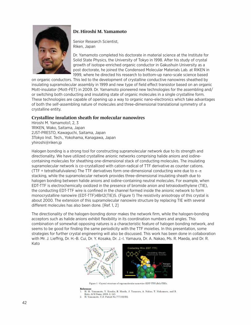
42
Dr. Hiroshi M. Yamamoto
Senior Research Scientist,Riken, Japan
Dr. Yamamoto completed his doctorate in material science at the Institute for Solid State Physics, the University of Tokyo in 1998. After his study of crystal growth of isotope-enriched organic conductor in Gakushuin University as a post doctorate, he joined the Condensed Molecular Materials Lab. at RIKEN in 1999, where he directed his research to bottom-up nano-scale science based
on organic conductors. This led to the development of crystalline conductive nanowires sheathed by insulating supramolecular assembly in 1999 and new type of fi eld eff ect transistor based on an organic Mott-insulator (Mott-FET) in 2009. Dr. Yamamoto pioneered new technologies for the assembling and/or switching both conducting and insulating state of organic molecules in a single crystalline form. These technologies are capable of opening up a way to organic nano-electronics which take advantages of both the self-assembling nature of molecules and three-dimensional translational symmetry of a crystalline entity.
Crystalline insulation sheath for molecular nanowiresHiroshi M. Yamamoto1, 2, 31RIKEN, Wako, Saitama, Japan2JST-PRESTO, Kawaguchi, Saitama, Japan3Tokyo Inst. Tech., Yokohama, Kanagawa, [email protected]
Halogen bonding is a strong tool for constructing supramolecular network due to its strength and directionality. We have utilized crystalline anionic networks comprising halide anions and iodine-containing molecules for sheathing one-dimensional stack of conducting molecules. The insulating supramolecular network is co-crystallized with cation-radical of TTF derivative as counter cations. (TTF = tetrathiafulvalene) The TTF derivatives form one-dimensional conducting wire due to stacking, while the supramolecular network provides three-dimensional insulating sheath due to halogen bonding between halide anions and iodine-containing neutral molecules. For example, when EDT-TTF is electrochemically oxidized in the presence of bromide anion and tetraiodoethylene (TIE), the conducting EDT-TTF wire is confi ned in the channel formed inside the anionic network to form monocrystalline nanowire (EDT-TTF)4BrI2(TIE)5. (Figure 1) The resistivity anisotropy of this crystal is about 2000. The extension of this supramolecular nanowire structure by replacing TIE with several diff erent molecules has also been done. [Ref. 1, 2]
The directionality of the halogen-bonding donor makes the network fi rm, while the halogen-bonding acceptors such as halide anions exhibit fl exibility in its coordination numbers and angles. This combination of somewhat opposing natures is a characteristic feature of halogen bonding network, and seems to be good for fi nding the same periodicity with the TTF moieties. In this presentation, some strategies for further crystal engineering will also be discussed. This work has been done in collaboration with Mr. J. Lieff rig, Dr. H.-B. Cui, Dr. Y. Kosaka, Dr. J.-I. Yamaura, Dr. A. Nakao, Ms. R. Maeda, and Dr. R. Kato
43
Dr. Oussama Moutanabbir
Professor,
Department of Engineering Physics,
Ecole Polytechnique de Montreal
Advanced Nanoscale and Hybrid Materials for Flexible Electronics, Photonics, Renewable Energy, and Bio-integrated Technologies.Dr. Oussama Moutanabbir, Dr. Norihiko Hayazawa
Our major focus is to develop novel semiconductor nanoscale and heterogeneous structures with controllable physical properties. We are in a unique position to establish innovative nanofabrication and integration methods to expand the capabilities of important semiconductors with the aim to enable integrative and fl exible systems with actual or potential impact on nanoelectronics, photonics, optoelectronics, carbon-free energy conversion, and bio-integrated technologies. A variety of novel complex and nanostructured materials will be implemented through this research thereby generating versatile building blocks for scalable, high-performance, and multifunctional nanodevices. Besides the technological importance, the availability of these materials will also provide a rich playground to investigate structural, mechanical, electrical, thermoelectric, electronic, and optical properties of diff erent semiconductors on the nano- and quantum scales.
These activities will be performed in close collaboration with RIKEN and will also involve the interaction with research groups and scientists from Keio University, AIST, and Mitsubishi Heavy Industries Ltd., with whom Prof. Moutanabbir has already signed independent agreements for collaboration in nanoscience and nanotechnology. The state-of-the-art nanofabrication facilities newly deployed at Ecole Polytechnique will be employed to establish innovative nanoscale and hybrid materials and devices. The basic properties and the performance of these nanomaterials and devices will be investigated using advanced nanoscale probes at RIKEN. This includes the use of one of the best laser-based probes in the world to study structural properties of materials and devices and test their stability [1]. This unique infrastructure will provide us with opportunities to explore a number of subtle but important phenomena such as phonon and heat transport on the nanoscale, which are critical for various applications in thermoelectrics and nanoelectronics to name a few.
Broader Impacts:
The proposed collaboration will off er our future students the opportunity to undertake worldclass, multidisciplinary research, to use approaches and experimental equipment that have never been mated heretofore, and to interact with researchers and engineers with diverse backgrounds.
This will help them gain a diversifi ed training and enrich their interpersonal skills, which are highly needed in an increasingly global and multicultural scientifi c research. We are also committed to create through this research close collaborations with research groups in Canada and abroad as well as with local and national industries. Progress in science on the nanoscale is crucial to ensure global competitiveness of the Canadian industry, which is in an excellent position to benefi t from trained highly qualifi ed personnel and locally generated intellectual properties.
44
Dr. Tohru Nakamura
(birth day: Jul/19/1965)
24-1, 1-Chome, Kami-Kashiwada, Ushiku-city,
Ibaraki-prefecture, zip-code 300-1232 JAPAN.
Tel, fax:+81-298-72-8121
e-mail: [email protected]
ExperienceNational Institute of Advanced Industrial Science and Technology (AIST)1-1-1 Higashi, Tsukuba-city, Ibaraki-prefecture, zip-code 305-8565 JAPANScientifi c studies, Research and DevelopmentPermanent Researcher, Dr, Research Team Leader: 2001-present
Agency of Industrial Science and Technology, Ministry of International Trade and Industry1-1-1 Higashi, Tsukuba-city, Ibaraki-prefecture, zip-code 305-8565 JAPANScientifi c studies, Research and Development Researcher, Dr: 1995-2000
Cranfi eld University, Cranfi eld, Bedfordshire, MK43 0AL, UKCollaboration with a Laboratory in Cranfi eld UniversityVisiting Researcher (supported by Science and Technology Agency, the Ministry of Education, Culture, Sports, Science and Technology): 2000-2001
EducationKyoto University (Organic Synthesis lab, Department of Chemistry, Faculty of Science)Okiwake, Kita-Shirakawa, Sakyoku, Kyoto, zip-code 606-8224 JAPANScientifi c StudiesDoctor of Chemistry, 1995Master of Chemistry, 1992
Additional InformationLanguage: Japanese, EnglishLicense: teacher’s certifi cate (chemistry), chemical materials, sanitary engineering
45
Autooxidized Monolayers of Organic Tellurium Compounds on GoldTohru NakamuraNanosystem Research Institute, AIST1-1-1 Higashi, Tsukuba, Ibarakli 305-8565, [email protected]
Tellurium (Te) is a semi-metal element located at the border between typical and metallic elements in the chalcogen group of the periodic table, so it shows intricate features, which lead to verifi ed reactivity and peculiarity in chemistry and material science of tellurium compounds. Fundamental studies and practical applications upon specifi c fi lms using the Te features have been developed considering their relation to giga- or tera-disk storage and IR detector component. Organic tellurium fi lms also revealed the specifi c characteristics and diversifi cation on metal surfaces such as silver and gold [1-7], where oxidized phenomena were observed presumably due to low fi rst ionization energy of tellurium - precious metal bonding systems.
The understanding of the interplay between substrate- anchoring group interactions and intermolecular interactions in organic monolayers plays a key role in exploring the fundamental research of surface science and developing industrial products. Many types of organic molecules with anchoring groups have been used to develop organic monolayers that are physically and chemically stable. Various anchoring groups using heteroatoms such as silicon (Si) and chalcogen (O, S, Se, Te) have been amply studied to obtain appropriate binders to solid surfaces.
Among them, ditelluride has been mainly using as an anchoring group of organic tellurium. It is particularly important that the properties of nanoelectronic interconnect between organic molecules and the metallic or semiconductive interfaces are controlled as a conductor or an insulator for the fabrication of molecular electronics. For example, interfaces with resistive and dielectric properties are crucial to fabricate nanodevices such as thin fi lm transistors. Chalcogenide groups are the simplest as junctions because chalcogens are able to directly connect the organic moiety and the inorganic surfaces with two covalent bonds. Along this line, we started to study previously unknown fi lms of heavy chalcogenide analogues with a view to tuning the electrical properties of organic molecular devices because heavy chalcogens (Se, Te) possess diff erent characters as compared with lighter chalcogens (O, S). It was found that dialkyl ditellurides adsorb on Au(111) surfaces by wet deposition to form highly resistive autooxidized monolayers (AMs) under air. The theoretical calculations suggested eff ective conducting properties of telluride systems. However, obtained conductivities of Te systems under ambient conditions are diff erent from that of the calculations.
We select ditellurides such as dibutyl and dioctyl ditelluride (R2Te2: R = Bu (n-C4H9), Oc (n-C8H17)) to form thin fi lms because tellurol, which is a thiol analogue, is generally unstable under ambient conditions. Dialkyl (Bu and Oc) disulfi des and diselenides were prepared as a control to compare with the ditellurides so that the contact resistances on the same alkyl group are similar in the conductivity measurements. Conductive AFM (c-AFM) measurements were performed by using a modifi ed SPA 300HV of Seiko Instruments Inc. under the vacuum conditions to reduce the eff ect of water molecules. We report here that the adsorption states and properties of organic tellurium fi lms including ditelluride form intriguing oxidized fi lms on the gold surfaces.
[References]
[1] Tohru Nakamura et al, Langmuir, 16, 4213-16 (2000). [2] Tohru Nakamura et al, Journal of Am. Chem. Soc., 124, 12642-43 (2002). [3] Tohru Nakamura et al, Langmuir, 21, 3344-53 (2005). [4] Tohru Nakamura et al, Langmuir, 21, 5026-33 (2005). [5] Joo, Sang-Woo, Journal of Raman Spectroscopy,37, 1244-47 (2006). [6] Tobias Weidner et al, Journal of Physical Chemistry C, 111, 11627-35 (2007). [7] Oana Bumbu et al, Inorganic Chemistry, 46, 11457-60 (2007).
46
Dr. Marianna FoldvariProfessor, Canada Research Chair,Bionanotechnology and Nanomedicine,Waterloo Institute for Nanotechnology,University of Waterloo [email protected]
Dr. Marianna Foldvari is the Canada Research Chair in Bionanotechnology and Nanomedicine. She is also a Professor of Pharmaceutical Sciences and served as the Associate Director, Research and Graduate Studies in the past 4 years, at the University of Waterloo’s School of Pharmacy. Dr. Foldvari’s expertise is in pharmaceutics, dosage form and drug delivery system design, nanotechnology, non-viral delivery methods, vaccine development, and computational modeling. She has over 20 years of experience as an academic researcher and in research and development in the pharmaceutical industry through technology transfer activities. Her research program is focusing on non-invasive drug delivery, gene therapy and pharmaceutical development of nano-enabled products. Dr Foldvari’s research is supported by grants from Canadian Institutes of Health Research (CIHR), Canada Foundation for Innovation (CFI) and Natural Sciences and Engineering Research Council of Canada (NSERC). Dr Foldvari is a member of the American Association for the Advancement of Science, American Association of Pharmaceutical Scientists, American Society for Gene and Cell Therapy and the Controlled Release Society. She currently serves as Associate Editor of Nanomedicine: Nanotechnology, Biology and Medicine and perform editorial activity for the Journal of Nanomedicine and Biotherapeutic Discovery, Current Patents in Nanomedicine, Journal of Bionanoscience, Current Drug Delivery, and International Journal of Pharmaceutical Compounding. Dr Foldvari served as a grant reviewer on CIHR, NSERC, CFI and NIH panels and the Bill and Melinda Gates Foundation Global Health Initiatives review board. Dr Foldvari is one of the Founding Directors of the American Society for Nanomedicine (ASNM) and the International Society of Nanomedicine (ISNM). She served as Board Member for Genome Prairie and was a Member of the Advisory Committee to the Prime Minister on Science and Technology and a Founder of the Canadian Society of Pharmaceutical Sciences (CSPS). She has received the YWCA Women of Distinction Award and the Sabex Award of Innovation. She is a frequently invited speaker at national and international conferences on gene and protein delivery systems and nanomedicine development and applications. Dr. Foldvari has authored more than 100 papers and 70 conference presentations and is the inventor on 18 patents. She founded two spin-off companies, PharmaDerm Laboratories Ltd. and DDS Research Inc., which focus on nanomedicine product development to commercialize technologies that she and her research team have developed. The Biphasix™ Technology (PharmaDerm/Helix BioPharma) Phase II/III investigational new drug (“IND”) application was submitted to the United States Food and Drug Administration (FDA) for Topical Interferon Alpha-2b for treatment of patients with low grade squamous intraepithelial lesions for the prevention of cervical cancer.
Non-invasive nanomedicines: Delivering an Army of Small and Large Molecules to do the JobMarianna Foldvari
The development and availability of eff ective drug delivery systems is becoming increasingly important for small molecules as well as for macromolecules such as proteins and DNA. Novel delivery systems have already had a major impact on drug therapies and patient wellbeing. For example, oral controlled-release systems, injectable sustained-release depots, polymeric brain implants, inhaler devices, liposomes, and quick-dissolve tablets were developed to provide patients with reliable and effi cient drug therapies. This presentation will focus on some recent protein and nucleic acid delivery systems, including their potential and limitations. In particular, the design and development of biphasic vesicles, gemini nanoparticles and carbon nanotubes as protein and DNA delivery systems will be presented. Biphasic vesicles (Biphasix™) represent a platform drug encapsulation technology suitable for delivering small drug molecules, proteins and vaccines. The Biphasix™ technology is a novel microscopic delivery system that could replace needles in the administration of proteins and genes, the pharmaceutical drugs of the future. Such large molecules generally can only be administered by painful injections and may not attain full therapeutic potential because they degrade before reaching the disease site. The fi rst application of the BiphasixTM is a topical interferon preparation currently in Phase II clinical trials for the treatment of ano-genital human papilloma virus (HPV) infections.Gemini nanoparticles (dicationic surfactant-based nanoparticles) as non-viral carriers have the advantage of having, generally, low toxicity/immunogenicity, as well as no limitation with regard to the size of DNA that can be delivered. Characterization of the structural and physicochemical properties of these dicationic lipid-based DNA complexes by small-angle x-ray scattering (SAXS), zeta potential and particle size analysis indicate correlation between polymorphic fl exibility of the nanoparticles and cellular transfection effi ciency. Carbon nanotubes (CNTs) have many potential applications as pharmaceutical excipients. Their unusual properties, in particular their extreme length-to-diameter ratio, propensity for chemical functionalization and potential biocompatibility, make CNTs promising candidates as delivery vehicles for biologically active molecules, as targets for biophysical treatments and as templates for tissue growth and regeneration. Because CNTs are hollow, they also have the potential to transport drugs by nanofl uidic delivery. Applications of CNTs as drug excipients for small molecules as well as for protein- and gene-based pharmaceuticals are of particular interest, given their propensity to interact with charged macromolecules such as amino acids and nucleic acids. The successful development of novel drug delivery technologies will provide improved drug and gene therapies through better targeting and localization of drugs at disease sites, off er new options to use drug molecules that could not be delivered before and provide alternative routes for delivery.
Session 2 - N
anoBiomaterials/H
ealth Technology

47
Dr. Tamotsu Zako, PhD
PhD, Senior Research Scientist,Bioengineering Laboratory,RIKEN
Tamotsu Zako is Senior Research Scientist at Bioengineering laboratory, RIKEN institute, Japan. Dr. Zako studied Chemistry and Biotechnology at The University of Tokyo, and received his PhD in 2001. He studied Biophysics and Biochemistry at Waseda University and Tokyo University of
Agriculture and Technology as a postdoctoral fellow. He was a recipient of Research Fellowship for Young Scientist from the Japan Society for the Promotion of Science (JSPS). His main research interests include the investigation of the functions of nano-biomolecular systems such as proteins and the application of biomolecule-conjugated nanoparticles.
Function and application of protein molecules and bio-nanoparticlesTamotsu Zako and Mizuo Maeda
The principal purpose of our team is to explore new nano bio-functional molecular systems on the basis of analytical chemistry, biophysics, biochemistry and molecular biology. In this talk, I’d like to introduce some of our recent studies.
Chemistry and engineering of molecular chaperone protein
Molecular chaperone proteins play important roles in the cells to help protein folding. We have intensively studied bio-function of molecular chaperone Prefoldin. Prefoldin captures a protein-folding intermediate and transfers it to another chaperone called chaperonin for correct folding1-3. Besides this function, we found that Prefoldin could cause formation of toxic oligomeric assembly of amyloid-beta peptide, suggesting a possible new role in Alzheimer’s Diseases4, 5. We have also recently demonstrated that Prefoldin has novel bio-functions such as photocyclodimerization of 2-anthracenecarboxylic acid6 and Size-selective recognition of gold nanoparticles7.
Chemistry and engineering of formation of protein nano-size structure
A number of proteins and peptides have been found to aggregate into nano-size fi brils or oligomer structures that cause various diseases. We have found that thin and fl exible insulin fi laments were formed in a presence of a reducing agent, Tris (2-carboxyethyl) phosphine hydrochloride (TCEP). This novel fi lament showed much lower cell toxicity than intact insulin fi brils8. We will also introduce our recent attempt to examine their inner structures using novel luminescent-conjugate polythiophene (LCP) molecules.
Development of NIR nanophosphors for bio-imaging
Near infrared (NIR) light in the wavelength region between 800 and 2000 nm is very useful for bio-imaging due to minimal optical loss. We have developed rare earth ion-doped yttrium oxide nanoparticles that can be used for bioimaging using NIR region9, 10. This phosphor will be a powerful tool for imaging target molecule inside tissues.
Development of novel metamaterials using DNA self-organization
We are investigating the fabrication technique of the nano-scale metal structures that will be applied for creating visible light metamaterials in collaboration with Nano-functional photonics team in RIKEN Institute. The method of DNA- templated cyclic gold nanoparticles assembly using self- organized hybridization process has been developed11.
References: 1 J. Biol. Chem., 279, 31788-95 (2004), 2 J. Mol. Biol., 399, 628-36 (2010), 3 J. Mol. Biol., 364, 110-20 (2006) 4 FEBS J., 277, 1348-58 (2010) 5 FEBS J., 275, 5982-93 (2008), 6 Photochem.& Photobiol. Sci., 9, 655-60 (2010) 7 Chem. Phys. Lett., 501, 108-12 (2010), 8 Biophys. J., 96, 3331-40 (2009), 9 J. Nanomaterials, 2010, 491471 (2010), 10 Biochem. Biophys. Res. Commun., 381, 54-8 (2009), 11 Chem. Commun., 46, 6132-4 (2010)
48
Dr. Mark T. McDermott
Principal Investigator,Devices and Sensors/Genomic Health Initiative,National Institute for Nanotechnology (NINT)
Dr. McDermott received his B. Sc. (Cum Laude) in Chemistry from the University of Pittsburgh at Johnstown and Ph. D. in Analytical Chemistry from The Ohio State University under Professor R. McCreery. He was a postdoctoral fellow at Iowa State University under Professor M. Porter. He is now an Associate Professor of Chemistry at the University of Alberta and a Principal Investigator at NINT. He is currently Associate Chair of Graduate Studies in the Department if Chemistry and is the Chair of the Analytical Chemistry Division of the Canadian Society for Chemistry. His research interests include biosensing, molecular electronics, “green” nanomaterials and interfacial chemistry.
Nanomaterial enabled biosensingMark T. McDermott
The motivation of much of the biosensor development worldwide is the promise of diagnostic devices that produce a rapid and sensitive response and have multiplex capabilities. Nanofabrication and nanomaterials are playing an increasing large role in the development of such sensors. Eff orts at the National Institute for Nanotechnology (NINT) has resulted in several new optical/spectroscopic biosensor platforms including Encoded nano- and micro-particles, label-free multiplex sensing, NEMS/MEMS devices and cross reactive sensor arrays. NINT scientists have also developed specifi c technologies such as non-fouling surface chemistry, spotting devices, nanoporous materials, nanosctuctured fi lms, phage capture technology and high throughput screening on encoded microspheres. This presentation will provide a brief overview of nanomaterial enabled biosensor developments at NINT.
Dr. Naoki Kawazoe
Senior Researcher,Tissue Regeneration Materials Unit, International Center for Materials Nanoarchitectonics (MANA), National Institute for Materials Science (NIMS)kawazoe.naoki nims.go.jp
Dr. Naoki Kawazoe is a senior researcher at Tissue Regeneration Materials Unit, International Center for Materials Nanoarchitectonics (MANA), National Institute for Materials Science (NIMS) in Japan.
He received his Ph.D from the Department of Material Chemistry at Kyoto University in March 1999. Then, he became a teaching associate in the Department of Biological Science and Technology, The University of Tokushima. In April, 2000, he moved to Nara Institute of Science and Technology (NAIST) as a teaching associate and stayed there for two and half years. He worked as a postdoctoral researcher at National Institute of Advanced Industrial Science and Technology (AIST) and at Toray Industries collaborating with Prof. Tomoji Kawai’s laboratory in Osaka University. And he moved to NIMS in April, 2006 and has been working at Dr. Guoping Chen’s group since then.
His current area of interest is polymeric biomaterials for cell function manipulation developed by techniques such as surface modifi cation and micropatterning.
49
Photograft ed Polymer Surfaces for Cell Function ManipulationNaoki Kawazoe, Hongxu Lu, and Guoping Chen
Tissue Regeneration Materials Unit, International Center for Materials Nanoarchitectonics (MANA), National Institute for Materials Science (NIMS)
The surface properties of biomaterials, including chemical composition, nano- or microstructured morphology, wettability, and electrostatic property, are crusial for manipulation of cell functions such as adhesion, proliferation and diff erentiation. Here, we describe the eff ects of surfaces grafted with diff erent chargeable polymers on stem cell functions by culturing human mesenchymal stem cells (MSCs) on surfaces grafted or micropatterned with cationic polyallylamine (PAAm), anionic poly(acrylic acid) (PAAc), and neutral poly(ethylene glycol) (PEG) and poly(vinyl alcohol) (PVA).
Photoreactive PAAm, PAAc and PEG were chemically synthesized by introducing photoreactive azidophenyl groups in the polymers. The photoreactive polymers were grafted onto polystyrene cell culture plates by UV irradiation. MSCs were cultured in the polymer-grafted plates to investigate the eff ect of PAAm, PAAc and PEG on cell functions. The PAAm-grafted surface supported cell adhesion, proliferation, and chondrogenic and osteogenic diff erentiation. The PAAc-grafted and non-grafted polystyrene surfaces promoted cell adhesion, proliferation and osteogenic diff erentiation, but not chondrogenic diff erentiation. The PEG-grafted surface did not support cell adhesion, but promoted chondrogenic diff erentiation.
Furthermore, the photoreactive PAAm, PAAc and PVA were micropatterned on polystyrene cell culture plates by UV photolithography using a photomask. A striped micropattern of each polymer with a width of 200 m was formed on the polystyrene plate. The micropatterned surfaces were used for culture of MSCs to investigate their eff ects on the adipogenic diff erentiation of MSCs. The MSCs adhered to and proliferated evenly on the PAAm- and PAAc-patterned surfaces, while the cells formed a stripe micropattern on the PVA-micropatterned surface because the PVA-grafted strip regions did not support cell adhesion. After being cultured in adipogenic diff erentiation induction medium, the cells were stained with Oil Red-O to examine adipogenic diff erentiation. Positively stained cells were distributed evenly on the PAAm- and PAAc-patterned surfaces, while they showed a micropattern on the PVA-micropatterned surface. The MSCs cultured on the PAAm, PAAc, and polystyrene surfaces expressed adipogenesis gene markers. The PAAm, and PAAc, and polystyrene surfaces supported the adipogenesis of MSCs while the PVA-surface did not.
These results indicate that the adhesion, proliferation, and diff erentiation of MSCs were able to be manipulated by diff erent chargeable polymer-grafted surfaces.
50
Dr. Françoise M. Winnik
Faculty of Pharmacy and Department of Chemistry,
University of Montreal,
WPI International Center for Materials Nanoarchitectonics (MANA),
National Institute for Materials Science (NIMS)
Françoise Winnik was born and educated in France where she earned a Diplome d’Ingénieur chimiste of the Ecole Nationale Supérieure de Chimie de Mulhouse. She obtained her PhD in organic chemistry and photochemistry. After post-doctoral studies in medical genetics, she worked for 12 years as a research scientist in the Xerox Research Center of Canada. She joined McMaster University (Hamilton, ON) in 1993 as an Associate Professor in Chemistry and Physics. Since 2000, she holds a joint position as professor in the Faculty of Pharmacy and the Department of Chemistry of the Université de Montréal. Since 2011, she is a Principal investigator in the WPI Centre for Materials Nanoarchitectonics of the National Institute for Materials Science, Tsukuba, Japan. Her expertise encompasses the chemistry of water soluble, amphiphilic, synthetic and natural polymers, their self-assembly in water and their applications in nanomedicine and as delivery vehicles. Her group has pioneered the applications of microcalorimetry, such as pressure perturbation calorimetry (PPC), and fl uorescence techniques to study aqueous polymer solutions and of fi eld fl ow chromatography to analyze soft and metallic nanoparticles. Her collaborative studies with D. Maysinger (Pharmacology, McGill) have led to important contribution towards the understanding of the toxicity of nanoparticles. She is Executive Editor of Langmuir, the ACS journal of surface and colloid science
Nanoarchitectonics: New Paradigm in Nanoscience and NanobiologyFrançoise M. Winnik
The term nanoarchitectonics was coined in 2000 to describe a new conceptual approach to create new functions on the nanoscale level by arranging defi ned structural units in an intended pattern. This methodology relies on several tools, including controlled self-organization, chemical manipulation, fi eld-induced transformations, and theoretical modeling.
This concept can also be applied in nanomedicine, and nanobiology. For example, Nakanishi et al. reported photoactivatable glass/gold surfaces whereon adsorption/desorption of cell-repellent proteins or polymers is switched on in response to photocleavage of a 2-nitrobenzyl ester.1 A similar approach is also useful in stem cell-based therapy, an emerging innovative strategy for the treatment of a variety of diseases states. The success of this approach depends critically on the availability of substrates that can enhance the in vitro amplifi cation and diff erentiation of progenitor cells. Tanguay et al. recently demonstrated that phosphorylcholine-modifi ed chitosan (CH-PC) fi lms act as an eff ective and selective support matrix for endothelial progenitor cells (EPCs).2 Cell micro patterning allows one to monitor the migration and diff erentiation of EPCs on spatially regulated substrate surfaces, and as such it is a critical tool to unravel the mechanisms controlling the cell-cell and cell-substrate interactions, leading to the establishment of viable methods for harvesting cells for clinical studies.
Other examples will be presented, including results from researchers in Japan (MANA)3 and in Canada (Université de Montréal),2 as seen from the perspective of a Professor in a Canadian University who is also a Principal Investigator of MANA.
References1. J. Nakanishi et al., Supramol. Chem., 22, 396 (2010); S. Kaneko et al., Phys. Chem. Chem. Phys. 13, 4051 (2011).2. K. Tardif et al. Biomaterials, 32, 5046 (2011).3. P. Techawanitchai et al, Sci Technol. Adv. Mat. 12 044609 (2011); T. Atsushi et al., Nanomedicine, 5 1089 (2010)
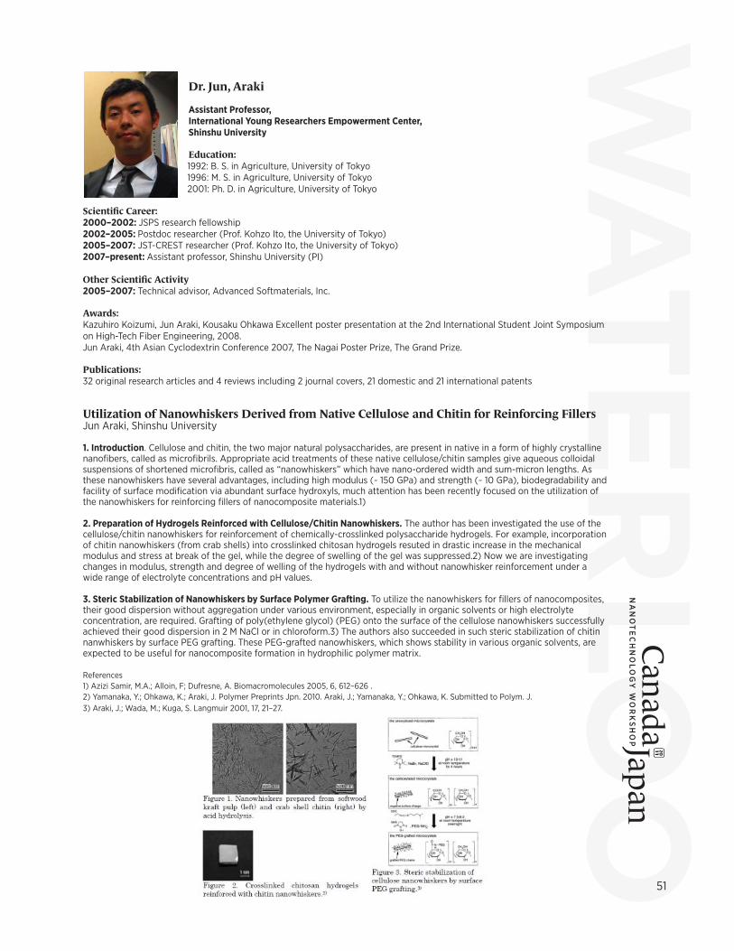
51
Dr. Jun, Araki
Assistant Professor,
International Young Researchers Empowerment Center,
Shinshu University
Education:1992: B. S. in Agriculture, University of Tokyo1996: M. S. in Agriculture, University of Tokyo2001: Ph. D. in Agriculture, University of Tokyo
Scientifi c Career:2000–2002: JSPS research fellowship2002–2005: Postdoc researcher (Prof. Kohzo Ito, the University of Tokyo)2005–2007: JST-CREST researcher (Prof. Kohzo Ito, the University of Tokyo)2007–present: Assistant professor, Shinshu University (PI)
Other Scientifi c Activity2005–2007: Technical advisor, Advanced Softmaterials, Inc.
Awards:Kazuhiro Koizumi, Jun Araki, Kousaku Ohkawa Excellent poster presentation at the 2nd International Student Joint Symposium on High-Tech Fiber Engineering, 2008.Jun Araki, 4th Asian Cyclodextrin Conference 2007, The Nagai Poster Prize, The Grand Prize.
Publications:32 original research articles and 4 reviews including 2 journal covers, 21 domestic and 21 international patents
Utilization of Nanowhiskers Derived from Native Cellulose and Chitin for Reinforcing FillersJun Araki, Shinshu University
1. Introduction. Cellulose and chitin, the two major natural polysaccharides, are present in native in a form of highly crystalline nanofi bers, called as microfi brils. Appropriate acid treatments of these native cellulose/chitin samples give aqueous colloidal suspensions of shortened microfi bris, called as “nanowhiskers” which have nano-ordered width and sum-micron lengths. As these nanowhiskers have several advantages, including high modulus (~ 150 GPa) and strength (~ 10 GPa), biodegradability and facility of surface modifi cation via abundant surface hydroxyls, much attention has been recently focused on the utilization of the nanowhiskers for reinforcing fi llers of nanocomposite materials.1)
2. Preparation of Hydrogels Reinforced with Cellulose/Chitin Nanowhiskers. The author has been investigated the use of the cellulose/chitin nanowhiskers for reinforcement of chemically-crosslinked polysaccharide hydrogels. For example, incorporation of chitin nanowhiskers (from crab shells) into crosslinked chitosan hydrogels resuted in drastic increase in the mechanical modulus and stress at break of the gel, while the degree of swelling of the gel was suppressed.2) Now we are investigating changes in modulus, strength and degree of welling of the hydrogels with and without nanowhisker reinforcement under a wide range of electrolyte concentrations and pH values.
3. Steric Stabilization of Nanowhiskers by Surface Polymer Grafting. To utilize the nanowhiskers for fi llers of nanocomposites, their good dispersion without aggregation under various environment, especially in organic solvents or high electrolyte concentration, are required. Grafting of poly(ethylene glycol) (PEG) onto the surface of the cellulose nanowhiskers successfully achieved their good dispersion in 2 M NaCl or in chloroform.3) The authors also succeeded in such steric stabilization of chitin nanwhiskers by surface PEG grafting. These PEG-grafted nanowhiskers, which shows stability in various organic solvents, are expected to be useful for nanocomposite formation in hydrophilic polymer matrix.
References1) Azizi Samir, M.A.; Alloin, F; Dufresne, A. Biomacromolecules 2005, 6, 612–626 .2) Yamanaka, Y.; Ohkawa, K.; Araki, J. Polymer Preprints Jpn. 2010. Araki, J.; Yamanaka, Y.; Ohkawa, K. Submitted to Polym. J.3) Araki, J.; Wada, M.; Kuga, S. Langmuir 2001, 17, 21–27.
52
Dr. Chris Backhouse
Professor,
Electrical and Computer Engineering,
Waterloo Institute for Nanotechnology,
University of Waterloo
Professor C. Backhouse (ECE) has extensive academic and industrial experience in the use of micro and nanofabrication technologies for the implementation and integration of nanobiotechnologies and quantum devices. The application area of his work ranges from healthcare and environmental monitoring to superconducting devices. He received his B.Sc. in Physics at the University of Alberta (Canada), followed by an M.Sc. (Radio Astronomy), and Ph.D. (Electrical Engineering) at the University of British Columbia (Canada). In industry, he led research teams in developing genetic analysis instrumentation based on microfl uidics, and medical imaging equipment based on high (Nb) and low (YBCO) temperature superconducting quantum devices. He was on faculty at the University of Alberta from 1999-2011 where he remains an Adjunct Professor. In July 2011, he joined the U. of Waterloo (ECE). In academia, his work has led to approximately 80 journal publications (>700 citations, H factor - 16). In 2009, a research team he led was awarded provincial (APEGGA) and national (Engineers Canada) engineering awards. Much of the research in his lab, the Applied Miniaturisation Laboratory (AML), is directed to making important technologies more accessible through miniaturisation and integration. Nowhere is this more important than in applying nanobiotechnologies where his lab seeks to integrate miniaturised optics, electronics, fl uidics and thermal systems to produce complete genetic diagnostics (from raw sample to fi nal result) in compact and inexpensive systems.
His research interests are; Quantum and nanoscale devices, Microsystem integrations of nanotechnologies, Controlling self-assembly at the molecular level, Lab on chip technologies and integrations for aff ordable healthcare, CMOS integration of LOC technologies
Inexpensive and Portable Medical Diagnostic SystemsChris Backhouse
The Lab on Chip (LOC) community worldwide has developed a tremendous range of technologies for the microuidics-based implementation of molecular biology procedures. However, although the LOC technologies are powerful, the complexity of the infrastructure required to support LOC operation has hindered the widespread adoption of LOC methods in life science applications. The work of the Backhouse lab is directed towards the development of inexpensive systems that enable implementations of a wide range of nanbiotechnological processes, both for medical diagnostics and for the exploration of nanoscale and self-assembly technologies.
Our laboratory has developed a range of LOC systems based on approaches that are suitable for low-cost, high-volume manufacture (i.e. scalable). As shown here (top right), we recently reported on a sample in, answer out system that can perform a medical diagnostic in approximately 1 hour. A Because of the scalability and modularity of our approach we have managed, on an ongoing basis, to halve our system cost each 6 months, ($600 in the above system). This system performed genetic amplifi cation via PCR followed by electrophoretic analysis using the microuidic chip shown here (middle right). This approach is highly reconfi gurable; for instance a variant of this system has been used (bottom right) for real-time PCR and melt curve analysis.
This same infrastructure and its applications to medical diagnostics provides an ideal platform for the exploration of self-assembly methods such as heteroduplex analysis. These methods provide interesting (and rapid ways) of analyzing DNA as well as allowing the formation of self-assembled structures under automated conditions. This talk will present the recent LOC work of the Backhouse lab with an emphasis on the development of extremely inexpensive (e.g. $100 to $1000) diagnostic systems and their application in the near-term for medical diagnostics and, in the longer term, an exploration of nanobiotechnologies.aKaigala et al., Analyst (2010) 135 1606-1617
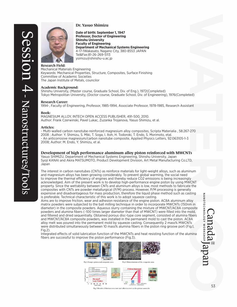
53
Dr. Yasuo Shimizu
Date of birth: September 1, 1947Professor, Doctor of EngineeringShinshu UniversityFaculty of EngineeringDepartment of Mechanical Systems Engineering4-17-1Wakasato, Nagano City, 380-8553 JAPANTel&Fax:[email protected]
Research Field:Mechanical Materials EngineeringKeywords: Mechanical Properties, Structure, Composites, Surface FinishingCommittee of Academic SocietiesThe Japan Institute of Metals, councilor
Academic Background:Shinshu University, (Master course, Graduate School, Div. of Eng.), 1972(Completed)Tokyo Metropolitan University, (Doctor course, Graduate School, Div. of Engineering), 1976(Completed)
Research Career:1994-, Faculty of Engineering, Professor, 1985-1994, Associate Professor, 1978-1985, Research Assistant
Book:MAGNESIUM ALLOY, INTECH OPEN ACCESS PUBLISHER, 491-500, 2010.Author: Frank Czerwinski, Pavel Lukac, Zuzanka Trojanova, Yasuo Shimizu, et al.
Articles:- Multi-walled carbon nanotube-reinforced magnesium alloy composites, Scripta Materialia , 58:267-270 2008 ; Author: Y. Shimizu, S. Miki, T. Soga, I. Itoh, H. Todoroki, T. Endo, S. Morimoto, etal.- An anticorrosive magnesium/carbon nanotube composite, Applied Physics Letters, 92:063105-1-3 2008; Author: M. Endo, Y. Shimizu, et al.
Development of high performance aluminum alloy piston reinforced with MWCNTsYasuo SHIMIZU, Department of Mechanical Systems Engineering, Shinshu University, JapanSyoji KANAI and Akira MATSUMOTO, Product Development Division, Art Metal Manufacturing Co.LTD, Japan
The interest in carbon nanotubes (CNTs) as reinforce materials for light-weight alloys, such as aluminum and magnesium alloys has been growing considerably. To prevent global warming, the social need to improve the thermal effi ciency of engines and thereby reduce CO2 emissions is being increasingly acknowledged. Aim of the present work is to develop high-performance engine piston by using MWCNT property. Since the wettability between CNTs and aluminum alloys is low, most methods to fabricate the composites with CNTs are powder metallurgical (P/M) process. However, P/M processing is generally expensive and disadvantageous for mass production, therefore the liquid phase method such as casting is preferable. Technical characteristic of this work is to adopt squeeze casting.Aims are to improve friction, wear and adhesion resistance of the engine piston. AC8A aluminum alloy matrix powders were subjected to the ball milling technique in order to incorporate MWCNTs (150nm in diameter) in the composite powders. Aqueous slurry containing the mixture of MWCNT/AC8A composite powders and alumina fi bers (~100 times larger diameter than that of MWCNT) were fi lled into the mold, and fi ltered and dried sequentially. Obtained porous disc-type core segment, consisted of alumina fi bers and MWCNT/AC8A composite powders, was installed in the permanent mold to cast the piston. AC8A alloy melt was poured into the permanent mold by squeeze casting. Consequently 2 mass% MWCNTs were distributed simultaneously between 10 mass% alumina fi bers in the piston ring groove port (Fig.1, Fig.2).Integrated eff ects of solid lubrication function of the MWCNTs and heat resisting function of the alumina fi bers are successful to improve the piston performance (Fig.3).
Session 4 - N
anostructures/Tools
54
Dr. Peter Mascher
William Sinclair Chair,
Optoelectronics,
McMaster University
Peter Mascher obtained a PhD in Engineering Physics in 1984 from the Graz University of Technology (TUG) in Austria and spent about four years as a post-doctoral fellow and research associate at the University of Winnipeg. He joined McMaster University in 1989 in a position initially funded by the Ontario Centre for Materials Research. He is a professional engineer and a professor in the Department of Engineering Physics, was Chair of the Department from 1995 to 2001, and since 2003 serves as the Associate Dean (Research and External Relations) of the Faculty of Engineering, with responsibilities for coordinating major research initiatives and collaborations of the Faculty. He also holds the William Sinclair Chair in Optoelectronics that was created by William Sinclair, one of the co-founders of JDS-Fitel, now part of JDS-Uniphase.
Dr. Mascher leads active research groups involved in the fabrication and characterization of thin fi lms for optoelectronic applications, the development and application of silicon-based nanostructures, and the characterization of defects in solids by positron annihilation spectroscopy. His research work is funded by the Natural Sciences and Engineering Research Council of Canada (NSERC), the Canada Foundation of Innovation (CFI), and several federal and provincial Centres of Excellence, as well as industry. He has supervised more than 40 Ph.D. and master’s degree students, has authored or coauthored more than 200 publications in refereed journals and conference proceedings, and has presented many invited lectures at international conferences and workshops. He is a member of the Steering Committee of the bi-annual Canadian Semiconductor Technology Conference (CSTC) and was the Conference Chair for the 14th CSTC and the 4th International Forum on Nano and Giga Challenges in Electronics, Photonics and Renewable Energy held jointly at McMaster University in Hamilton in August 2009. In 2006, he co-chaired the 14th International Conference on Positron Annihilation, also held at McMaster. As a member of the executive body of the Dielectric Sciences and Technology Division of the Electrochemical Society, Dr. Mascher has led and organized several international symposia on the Science and Technology of Dielectrics for Active and Passive Devices and on Nanocrystal Embedded Dielectrics for Electronic and Photonic Devices and most recently, an international symposium on Nanoscale Luminescent Materials.
From 2003 to 2007 Dr. Mascher served as the Program Director of the Ontario Photonics Consortium, and he currently is a member of the Board of Management of the Ontario Photonics Industry Network (OPIN), the Centre of Photonics of Ontario Centres of Excellence (OCE), and Nano-Ontario. In 2009, he led a successful $6M multi-university CFI New Initiatives Fund application to transform the McMaster Research Reactor into one of the world’s brightest positron sources for materials and fundamental research.
Fabrication and Characterization of Semiconductor Nanostructures for Photonics ApplicationsPeter Mascher
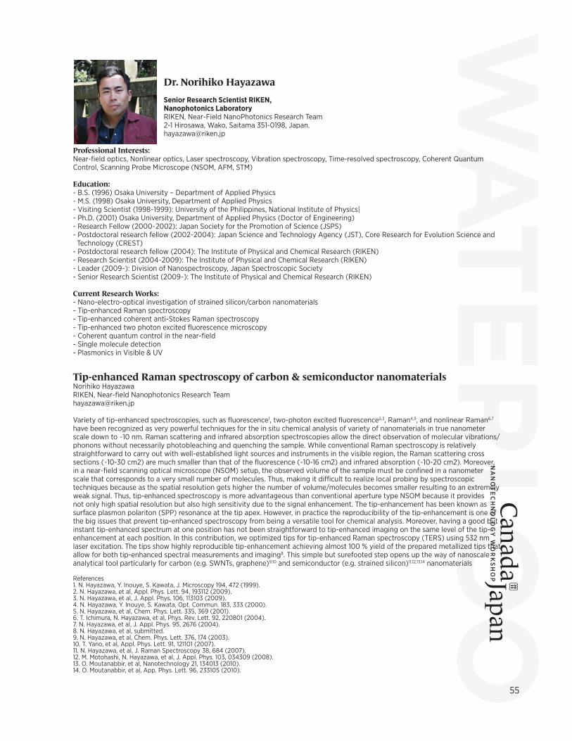
55
Dr. Norihiko HayazawaSenior Research Scientist RIKEN,
Nanophotonics Laboratory
RIKEN, Near-Field NanoPhotonics Research Team 2-1 Hirosawa, Wako, Saitama 351-0198, [email protected]
Professional Interests:Near-fi eld optics, Nonlinear optics, Laser spectroscopy, Vibration spectroscopy, Time-resolved spectroscopy, Coherent Quantum Control, Scanning Probe Microscope (NSOM, AFM, STM)
Education:- B.S. (1996) Osaka University – Department of Applied Physics- M.S. (1998) Osaka University, Department of Applied Physics- Visiting Scientist (1998~1999): University of the Philippines, National Institute of Physics|- Ph.D. (2001) Osaka University, Department of Applied Physics (Doctor of Engineering)- Research Fellow (2000~2002): Japan Society for the Promotion of Science (JSPS)- Postdoctoral research fellow (2002~2004): Japan Science and Technology Agency (JST), Core Research for Evolution Science and Technology (CREST)- Postdoctoral research fellow (2004): The Institute of Physical and Chemical Research (RIKEN)- Research Scientist (2004~2009): The Institute of Physical and Chemical Research (RIKEN)- Leader (2009~): Division of Nanospectroscopy, Japan Spectroscopic Society- Senior Research Scientist (2009~): The Institute of Physical and Chemical Research (RIKEN)
Current Research Works:- Nano-electro-optical investigation of strained silicon/carbon nanomaterials- Tip-enhanced Raman spectroscopy- Tip-enhanced coherent anti-Stokes Raman spectroscopy- Tip-enhanced two photon excited fl uorescence microscopy- Coherent quantum control in the near-fi eld- Single molecule detection- Plasmonics in Visible & UV
Tip-enhanced Raman spectroscopy of carbon & semiconductor nanomaterialsNorihiko HayazawaRIKEN, Near-fi eld Nanophotonics Research [email protected]
Variety of tip-enhanced spectroscopies, such as fl uorescence1, two-photon excited fl uorescence2,3, Raman4,5, and nonlinear Raman6,7 have been recognized as very powerful techniques for the in situ chemical analysis of variety of nanomaterials in true nanometer scale down to ~10 nm. Raman scattering and infrared absorption spectroscopies allow the direct observation of molecular vibrations/phonons without necessarily photobleaching and quenching the sample. While conventional Raman spectroscopy is relatively straightforward to carry out with well-established light sources and instruments in the visible region, the Raman scattering cross sections (~10-30 cm2) are much smaller than that of the fl uorescence (~10-16 cm2) and infrared absorption (~10-20 cm2). Moreover, in a near-fi eld scanning optical microscope (NSOM) setup, the observed volume of the sample must be confi ned in a nanometer scale that corresponds to a very small number of molecules. Thus, making it diffi cult to realize local probing by spectroscopic techniques because as the spatial resolution gets higher the number of volume/molecules becomes smaller resulting to an extremely weak signal. Thus, tip-enhanced spectroscopy is more advantageous than conventional aperture type NSOM because it provides not only high spatial resolution but also high sensitivity due to the signal enhancement. The tip-enhancement has been known as surface plasmon polariton (SPP) resonance at the tip apex. However, in practice the reproducibility of the tip-enhancement is one of the big issues that prevent tip-enhanced spectroscopy from being a versatile tool for chemical analysis. Moreover, having a good but instant tip-enhanced spectrum at one position has not been straightforward to tip-enhanced imaging on the same level of the tip-enhancement at each position. In this contribution, we optimized tips for tip-enhanced Raman spectroscopy (TERS) using 532 nm laser excitation. The tips show highly reproducible tip-enhancement achieving almost 100 % yield of the prepared metallized tips that allow for both tip-enhanced spectral measurements and imaging8. This simple but surefooted step opens up the way of nanoscale analytical tool particularly for carbon (e.g. SWNTs, graphene)9,10 and semiconductor (e.g. strained silicon)11,12,13,14 nanomaterials
References1. N. Hayazawa, Y. Inouye, S. Kawata, J. Microscopy 194, 472 (1999).2. N. Hayazawa, et al, Appl. Phys. Lett. 94, 193112 (2009).3. N. Hayazawa, et al, J. Appl. Phys. 106, 113103 (2009).4. N. Hayazawa, Y. Inouye, S. Kawata, Opt. Commun. 183, 333 (2000).5. N. Hayazawa, et al, Chem. Phys. Lett. 335, 369 (2001).6. T. Ichimura, N. Hayazawa, et al, Phys. Rev. Lett. 92, 220801 (2004).7. N. Hayazawa, et al, J. Appl. Phys. 95, 2676 (2004).8. N. Hayazawa, et al, submitted.9. N. Hayazawa, et al, Chem. Phys. Lett. 376, 174 (2003).10. T. Yano, et al, Appl. Phys. Lett. 91, 121101 (2007).11. N. Hayazawa, et al, J. Raman Spectroscopy 38, 684 (2007).12. M. Motohashi, N. Hayazawa, et al, J. Appl. Phys. 103, 034309 (2008).13. O. Moutanabbir, et al, Nanotechnology 21, 134013 (2010).14. O. Moutanabbir, et al, App. Phys. Lett. 96, 233105 (2010).
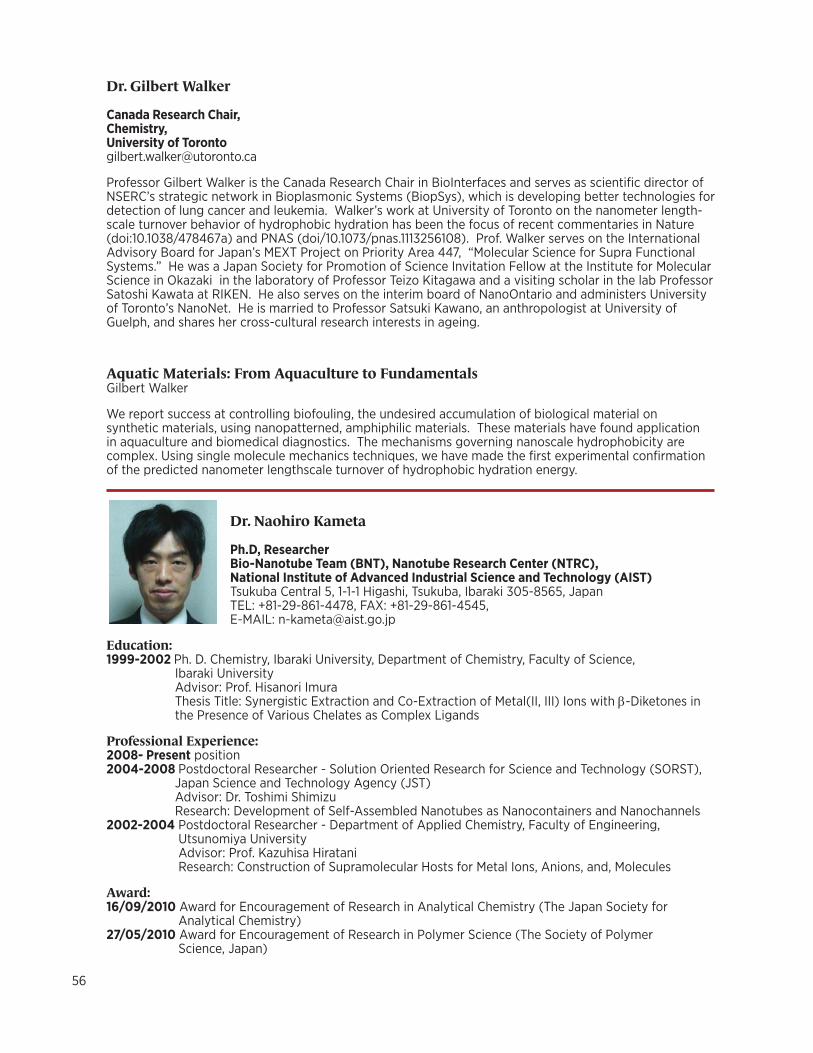
56
Dr. Gilbert Walker
Canada Research Chair,Chemistry,University of [email protected]
Professor Gilbert Walker is the Canada Research Chair in BioInterfaces and serves as scientifi c director of NSERC’s strategic network in Bioplasmonic Systems (BiopSys), which is developing better technologies for detection of lung cancer and leukemia. Walker’s work at University of Toronto on the nanometer length-scale turnover behavior of hydrophobic hydration has been the focus of recent commentaries in Nature (doi:10.1038/478467a) and PNAS (doi/10.1073/pnas.1113256108). Prof. Walker serves on the International Advisory Board for Japan’s MEXT Project on Priority Area 447, “Molecular Science for Supra Functional Systems.” He was a Japan Society for Promotion of Science Invitation Fellow at the Institute for Molecular Science in Okazaki in the laboratory of Professor Teizo Kitagawa and a visiting scholar in the lab Professor Satoshi Kawata at RIKEN. He also serves on the interim board of NanoOntario and administers University of Toronto’s NanoNet. He is married to Professor Satsuki Kawano, an anthropologist at University of Guelph, and shares her cross-cultural research interests in ageing.
Aquatic Materials: From Aquaculture to FundamentalsGilbert Walker
We report success at controlling biofouling, the undesired accumulation of biological material on synthetic materials, using nanopatterned, amphiphilic materials. These materials have found application in aquaculture and biomedical diagnostics. The mechanisms governing nanoscale hydrophobicity are complex. Using single molecule mechanics techniques, we have made the fi rst experimental confi rmation of the predicted nanometer lengthscale turnover of hydrophobic hydration energy.
Dr. Naohiro Kameta
Ph.D, ResearcherBio-Nanotube Team (BNT), Nanotube Research Center (NTRC), National Institute of Advanced Industrial Science and Technology (AIST)Tsukuba Central 5, 1-1-1 Higashi, Tsukuba, Ibaraki 305-8565, JapanTEL: +81-29-861-4478, FAX: +81-29-861-4545, E-MAIL: [email protected]
Education:1999-2002 Ph. D. Chemistry, Ibaraki University, Department of Chemistry, Faculty of Science, Ibaraki University Advisor: Prof. Hisanori Imura Thesis Title: Synergistic Extraction and Co-Extraction of Metal(II, III) Ions with -Diketones in the Presence of Various Chelates as Complex Ligands
Professional Experience:2008- Present position2004-2008 Postdoctoral Researcher - Solution Oriented Research for Science and Technology (SORST), Japan Science and Technology Agency (JST) Advisor: Dr. Toshimi Shimizu Research: Development of Self-Assembled Nanotubes as Nanocontainers and Nanochannels2002-2004 Postdoctoral Researcher - Department of Applied Chemistry, Faculty of Engineering, Utsunomiya University Advisor: Prof. Kazuhisa Hiratani Research: Construction of Supramolecular Hosts for Metal Ions, Anions, and, Molecules
Award:16/09/2010 Award for Encouragement of Research in Analytical Chemistry (The Japan Society for Analytical Chemistry)27/05/2010 Award for Encouragement of Research in Polymer Science (The Society of Polymer Science, Japan)

57
Construction of Self-Assembled Soft Nanotubes and Exploitation of Their FunctionsNaohiro Kameta (Ph.D, Researcher)Nanotube Research Center (NTRC), National Institute of Advanced Industrial Science and Technology (AIST)[email protected]
Bottom-up nanotechnology based on supramolecular and biomimetic chemistry enabled us to produce tubular nanoarchitectures. We have already reported that well-designed synthetic glyoco- and peptide-lipids self-assembled in water to form tubular structures (abbreviated as nanotubes hereafter) having hydrophilic channels with 5-100 nm inner diameters.1 The nanotubes consist of bilayer membranes, and have same inner and outer surfaces covered with hydrophilic headgroups of the lipids. If we can functionalize each surface of the nanotubes, the functionalized nanotubes should have some advantages, especially for encapsulation and release of guests. Herein, we describe construction of nanotubes with functionalized surfaces and controlled diameters, and exploitation of their functions related to the hydrophilic channel. Wedge-shaped amphiphiles having diff erent sized headgroups at both ends self-assembled in water to form nanotubes with precisely controlled inner diameters.2,3 Molecular packing analysis showed that the obtained nanotubes consist of monolayer membrane, and have diff erent inner and outer surfaces covered with each headgroups. The nanotubes were able to encapsulate hydrophilic biomacromolecules and nanoparticles in the channel and fi x hydrophobic low-weight molecules including drugs within the membrane wall.4,5 On the other hand, the capsulated guests were controllably released by outer stimuli such as pH, temperature, and light.6,7 Selective introduction of sensing probe into the nanotube inner surface enabled us to directly detect dynamic behavior of proteins in the nanotube channel.8,9 The diff usion constants of proteins were remarkably smaller than those of free proteins in bulk solutions. Such confi ned proteins in the nanotube channel had high resistance to denaturants and high temperatures.10,11 Namely, the nanotubes were able to stabilize proteins under chemically and thermally unfavorable conditions. Furthermore, the nanotubes acted as an artifi cial chaperon, and strongly assisted the refolding of denatured proteins in the channel.12 Thus, soft nanomaterials based on the nanotube should be widely applicable to biological and medical fi elds.
References [1] N. Kameta et al., Soft Matter (Review article) 7, 4539 (2011). [2] N. Kameta et al., Chem. Lett. 36, 896 (2007). [3] N. Kameta et al., Langmuir 23, 4634 (2007). [4] N. Kameta et al., Adv. Mater. 17, 2732 (2005). [5] N. Kameta et al., Soft Matter 7, 85 (2011). [6] N. Kameta et al., Soft Matter 4, 1681 (2008). [7] N. Kameta et al., Chem. Eur. J. 17, 5251 (2011). [8] N. Kameta et al., Chem. Mater. 19, 3553 (2007). [9] N. Kameta et al., Small 4, 561 (2008). [10] N. Kameta et al., Chem. Mater. 21, 5892 (2009). [11] N. Kameta et al., Chem. Eur. J. 16, 4217 (2010). [12] N. Kameta et al., in preparation.
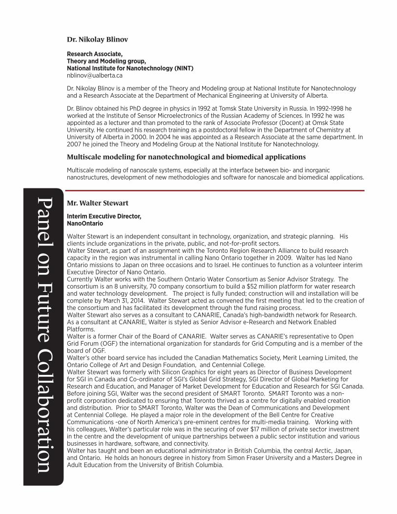
58
Dr. Nikolay Blinov
Research Associate,
Theory and Modeling group,
National Institute for Nanotechnology (NINT)
Dr. Nikolay Blinov is a member of the Theory and Modeling group at National Institute for Nanotechnology and a Research Associate at the Department of Mechanical Engineering at University of Alberta.
Dr. Blinov obtained his PhD degree in physics in 1992 at Tomsk State University in Russia. In 1992-1998 he worked at the Institute of Sensor Microelectronics of the Russian Academy of Sciences. In 1992 he was appointed as a lecturer and than promoted to the rank of Associate Professor (Docent) at Omsk State University. He continued his research training as a postdoctoral fellow in the Department of Chemistry at University of Alberta in 2000. In 2004 he was appointed as a Research Associate at the same department. In 2007 he joined the Theory and Modeling Group at the National Institute for Nanotechnology.
Multiscale modeling for nanotechnological and biomedical applications
Multiscale modeling of nanoscale systems, especially at the interface between bio- and inorganic nanostructures, development of new methodologies and software for nanoscale and biomedical applications.
Mr. Walter Stewart
Interim Executive Director,
NanoOntario
Walter Stewart is an independent consultant in technology, organization, and strategic planning. His clients include organizations in the private, public, and not-for-profi t sectors. Walter Stewart, as part of an assignment with the Toronto Region Research Alliance to build research capacity in the region was instrumental in calling Nano Ontario together in 2009. Walter has led Nano Ontario missions to Japan on three occasions and to Israel. He continues to function as a volunteer interim Executive Director of Nano Ontario. Currently Walter works with the Southern Ontario Water Consortium as Senior Advisor Strategy. The consortium is an 8 university, 70 company consortium to build a $52 million platform for water research and water technology development. The project is fully funded; construction will and installation will be complete by March 31, 2014. Walter Stewart acted as convened the fi rst meeting that led to the creation of the consortium and has facilitated its development through the fund raising process.Walter Stewart also serves as a consultant to CANARIE, Canada’s high-bandwidth network for Research. As a consultant at CANARIE, Walter is styled as Senior Advisor e-Research and Network Enabled Platforms.Walter is a former Chair of the Board of CANARIE. Walter serves as CANARIE’s representative to Open Grid Forum (OGF) the international organization for standards for Grid Computing and is a member of the board of OGF. Walter’s other board service has included the Canadian Mathematics Society, Merit Learning Limited, the Ontario College of Art and Design Foundation, and Centennial College.Walter Stewart was formerly with Silicon Graphics for eight years as Director of Business Development for SGI in Canada and Co-ordinator of SGI’s Global Grid Strategy, SGI Director of Global Marketing for Research and Education, and Manager of Market Development for Education and Research for SGI Canada. Before joining SGI, Walter was the second president of SMART Toronto. SMART Toronto was a non-profi t corporation dedicated to ensuring that Toronto thrived as a centre for digitally enabled creation and distribution. Prior to SMART Toronto, Walter was the Dean of Communications and Development at Centennial College. He played a major role in the development of the Bell Centre for Creative Communications -one of North America’s pre-eminent centres for multi-media training. Working with his colleagues, Walter’s particular role was in the securing of over $17 million of private sector investment in the centre and the development of unique partnerships between a public sector institution and various businesses in hardware, software, and connectivity.Walter has taught and been an educational administrator in British Columbia, the central Arctic, Japan, and Ontario. He holds an honours degree in history from Simon Fraser University and a Masters Degree in Adult Education from the University of British Columbia.
Panel on Future Collaboration
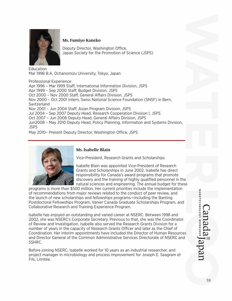
59
Ms. Fumiyo Kaneko
Deputy Director, Washington Offi ce,Japan Society for the Promotion of Science (JSPS)
EducationMar 1996 B.A. Ochanomizu University, Tokyo, Japan
Professional ExperienceApr 1996 – Mar 1999 Staff , International Information Division, JSPSApr 1999 – Sep 2000 Staff , Budget Division, JSPSOct 2000 – Nov 2000 Staff , General Aff airs Division, JSPSNov 2000 – Oct 2001 Intern, Swiss National Science Foundation (SNSF) in Bern, SwitzerlandNov 2001 – Jun 2004 Staff , Asian Program Division, JSPSJul 2004 – Sep 2007 Deputy Head, Research Cooperation Division I, JSPSOct 2007 – Jun 2008 Deputy Head, General Aff airs Division, JSPSJun2008 – May 2010 Deputy Head, Policy Planning, Information and Systems Division, JSPSMay 2010– Present Deputy Director, Washington Offi ce, JSPS
Ms. Isabelle Blain
Vice-President, Research Grants and Scholarships
Isabelle Blain was appointed Vice-President of Research Grants and Scholarships in June 2002. Isabelle has direct responsibility for Canada’s award programs that promote discovery and the training of highly qualifi ed personnel in the natural sciences and engineering. The annual budget for these
programs is more than $500 million. Her current priorities include the implementation of recommendations from major reviews related to the conduct of peer review, and the launch of new scholarships and fellowships programs—including the Banting Postdoctoral Fellowships Program, Vanier Canada Graduate Scholarships Program, and Collaborative Research and Training Experience Program.
Isabelle has enjoyed an outstanding and varied career at NSERC. Between 1998 and 2002, she was NSERC’s Corporate Secretary. Previous to that, she was the Coordinator of Review and Investigation. Isabelle also served the Research Grants Division for a number of years in the capacity of Research Grants Offi cer and later as the Chief of Coordination. Her interim appointments have included the Director of Human Resources and Director General of the Common Administrative Services Directorate of NSERC and SSHRC.
Before joining NSERC, Isabelle worked for 10 years as an industrial researcher, and project manager in microbiology and process improvement for Joseph E. Seagram et Fils, Limitée.
60
Dr. Hamdy Khalil
Global Technical Director for Research and Product Development,
Woodbridge Foam Corporation, The Woodbridge Group
Dr. Hamdy Khalil pioneered the introduction and commercialization of renewable materials into the polyurethane chemistry used in the interior automotive parts manufacturing which is now the benchmark for the industry.
Prior to his present position at Woodbridge Foam Corporation - a major manufacturer of fl exible moulded polyurethane foam for the global automotive industry- Hamdy held positions at Labatt’s in the pharmaceutical Division, for PolySar Corporation as analytical laboratory supervisor and as Senior Technical Manager for BFGoodrich.
He introduced and published groundbreaking chemistries in:- Reformatsky Reaction to Synthesize Vitamin A Analogues- Wittig Reaction in the Synthesis of Polyene- Phase transfer catalysis for the synthesis of hitherto known Sulfur and Oxygen Heterocyclic fi ve and six member Compounds useful in Pheromones and Pharmaceuticals
He has coauthored patents in:- Polyurethane Structural Sealants for Automotive Windshield Fastening- High Impact Polystyrene Light Stability- Latex Anti-Microbial Growth Additives- Bio-Polyol in Automotive Parts Manufacturing
Hamdy sits on the scientifi c advisory committee of FPInnovations and on the NRC steering committee for Bio-products development. His fi rst passion is the mentoring and the customized development of young scientists and technical personnel.
Dr. Khalil holds a BSc with majors in chemistry and physics from the University of Alexandria in Egypt, MSc in Nutritional Biochemistry from Cairo University Egypt and a PhD from Windsor University.
61
Mr. Marc Mikhael
Trade Commissioner, Innovation, Science and Technology Division, Department of Foreign Aff airs and International Trade
Marc Mikhael is the trade commissioner responsible for bilateral science and technology cooperation with China at the Innovation, Science and Technology Division of the Department of Foreign Aff airs and International Trade (DFAIT).
Prior to joining the Innovation, Science and Technology Division, Marc served as a vice consul at the Consulate General of Canada in Shanghai. Marc holds a Bachelor of Applied Science in Computer Engineering from the University of Ottawa.
Dr. Yoichi Miyahara
Research Associate, Department of Physics,NanoScience and Scanning Probe Microscopy Group,[email protected]/SPM/index.html
Research Areas:• Nanoelectronics• Quantum dot devices• Magnetic quantum cellular automata• Molecular electronics• Electronic transport through single-molecule• Nanomechanics• Nano/Atomic scale indentation • Scanning probe microscopy instrumentation• Electric force microscopy• Frequency modulation mode atomic force microscopy• Cantilever dynamics
Education:Dr. Eng., Waseda UniversityM. Eng., Waseda UniversityB. Eng., Waseda University
Ms. Ayako Murata
Technical Staff , International Contracts Team (MOU),International Cooperation Offi ce, International Aff airs Division,Research and Innovation Promotion Headquarters,National Institute of Advanced Industrial Science and Technology (AIST)
Education:September 1999 – May 2004 BA in Communication Studies, University of Nevada, RenoApril 1998 – March 1999 Nevada-California International Consortium of Universities & Colleges in Japan (NIC)
Work Experience:October 2010 - Present Technical Staff , International Contracts Team (MOU), International Cooperation Offi ce, International Aff airs Division, Research and Innovation Promotion Headquarters, AIST Tsukuba, Ibaraki, JapanApril 2008 – September 2010Technical Staff , International Contracts Team (Joint Research), International Relations Offi ce, International Aff airs Department, AIST Tsukuba, Ibaraki, JapanSeptember 2005 – March 2008Secretary, Asia-Pacifi c Legal Metrology Forum (APLMF), National Metrology Institute of Japan (NMIJ), AIST Tsukuba, Ibaraki, Japan
Awards:April 2011 AIST President Award, Contribution to enhancing the procedural effi ciency in international joint research contractingOctober 2008 APLMF Service Award, Contribution to the APLMF activities as the SecretaryJanuary 2008 NMIJ Service Award, Contribution to the APLMF training courses in legal metrology
Invited Attendees
62
Mr. Masahiro Takemura
Offi ce Chief, Research and Analysis Offi ceNational Institute for Materials Science (NIMS)1-2-1 Sengen, Tsukuba, Ibaraki 305-0047 JapanPhone: +81-29-859-2402, Fax: +81-29-859-2049E-mail: [email protected]: http://www.nims.go.jp/eng
Education:March, 1985 B. Eng., Aeronautics, University of Tokyo, JapanMarch, 1987 M. Eng., Aeronautics, University of Tokyo, JapanJune, 1995 M. S., Materials Science, University of Illinois at Chicago, USA
Professional Appointments:April, 1987 Researcher, Steel Research Center, NKK Corp.August, 1995 Senior Researcher, Materials & Processing Research Center, NKK Corp.April, 2003 Senior Researcher, Steel Research Center, JFE Steel Corp. (merger with Kawasaki Steel Corp.)September, 2003 Senior Researcher, Nanotechnology Researchers Network Center of Japan (Nanonet), NIMSApril, 2006 Manager, International Aff airs Offi ce, NIMSSeptember, 2007 General Manager, International Aff airs Offi ce, Planning Division, NIMSApril, 2011 Offi ce Chief, Research and Analysis Offi ce
Mr. Alain FrancqManaging Director,Waterloo Institute for Nanotechnology,University of [email protected]
As Managing Director of the Waterloo Institute for Nanotechnology, Mr Francq is accountable for the day-to-day business operations of the Institute and for developing industry, academic and government partnerships in Nanotechnology research. Together, with the Executive Director, the Managing Director is responsible for:
Defi ning and advancing the overall goals of WIN with its members, directors and the advisory boards.
Fostering meaningful interactions with prospective industry, academic and government partners and stewarding existing collaborations.
• Raising the profi le of the Institute and it’s researchers by planning and implementing a wide range of marketing and communications initiatives.
• Managing large infrastructure and operating research projects, including proposal development, budgeting, fi nancial and technical reporting.
• Managing administrative and supervisory functions, including human resources, fi nance and space management.
Alain Francq worked as a University lecturer and he is currently Vice-Chair of the International Business Management (IBM) program advisory committee at Conestoga College, Ontario, Canada. Prior to joining the University of Waterloo, he worked in Canada’s science and technology sector for several spin-off companies that have commercialized Intellectual Property from the University of Waterloo. Mr Francq holds an Honors Bachelor of Science (BSc.) degree from the University of Waterloo (UW) and a Masters of Business Administration (MBA) degree from Wilfrid Laurier University in International Business and Commercialization of Science and Technology.
The University of Waterloo has profound existing strengths in nanotechnology. The campus is home to world-class researchers, fl agship research facilities ($160 million dollar, 284 000 square foot Quantum-Nano Centre), and Canada’s largest nanotechnology undergraduate engineering program with over 450 students. The Waterloo Institute for Nanotechnology is comprised of 60 faculty members, 17 Research Chairs from 9 departments who perform research in Nano-Materials, Nano-Electronics, Nano-Devices and Nano-Biosystems. Mr Francq was the co-lead organizer of NanoForum Canada (2006), the Ontario-India Nanotechnology Workshop (2006), the Canada-India Nanotechnology workshop (2008), and the Canada-Japan Nanotechnology Workshop (2011).
Workshop O
rganizers
63
64
www.nano.uwaterloo.ca/Japan-Canada-Nanotechnology-Workshop