Embed Size (px)
Citation preview
APPLICATION OF COMPUTERS TO CIRCUIT DESIGN FOR UNIVAC LARC
Gilbert Kaskey Associate Division Director. Systems Design and Application
Remington Rand Univac Philadelphia. Pennsylvania
Noah S. Prywes Consultant to Remington Rand Univac
Assistant Professor. Moore School. University of Pennsylvania Philadelphia. Pennsylvania
Herman Lukoff Chief Engineer. Remington Rand Univac
Philadelphia. Pennsylvania
The design of circuits for computers has become in recent years a complex undertaking. The problem is two-fold. On one hand optimization of cost and speed is the prime objective. On the other hand. complexity is increased through factors such as component charact~ristics and life expectancy. manufacturing techniques. and the suppression of noise in very large systems. The complexity makes the use of computers as an aid to design almost imperative; this was the case in the desi.gn of circuits for Univac Larc.
Several applications of computers in circuit design are reported here and demonstrated by case histories for Univac Larc. The paper consists of two parts. In Part I. a general description of the problems and solutions is given. References to available reports or publications are given where a more detailed description can be found. The problem areas can be divided into three categories: evaluation of components and life test; design of circuits; protection against noise. Part II consists of a detailed description of the statistical techniques used in the circuit design.
Part I
A. Evaluation of Components and Life Tests
Evaluation of Components. The components evaluated included transistors. diodes. ferractors. ferrite cores. resistors. capacitors. etc. As an example. the evaluation of Philco surface barrier transistors will be reported here. This transistor was selected during the first half of 1956 after a study of many other candidates in respect to rise time. storage time. gain. current level at optimum performance and cost. The evaluation program required the testing of a large number of transistors to determine such parameters as beta. rise time. storage time. and breakdown voltage. These values were measured initially and at various times throughout life test.
In the attempt to mechanize the test data analysis. a complete library of Univac statistical routines has been developed. These statistical routines analyzed and evaluated the available data. The statistical analysis of empirical data is greatly simplified if the variate under analy-
sis is normally distributed. Since this is rarely the case in practice. the distributions were transformed to ones that have Gaussian properties.
Close cooperation with manufacturers was maintained to insure that the transistors received were the best that could be produced in the manufacturing process used. Experimental designs were made to aid in the determination of the effect of various changes in production techniques. e.g •• resistivity and etching time. on the several transistor parameters. A UNIVAC@ routine was then used to perform the analysis of variance necessary for the identification of the statistically significant variables. The results. a joint effort between the manufacturer and user. helped establish production control procedures which virtually insured that component lots would
meet the required specification. 5
Evaluation of Life Test. Because of the long life expectancy of transistors it was difficult to ascertain failure characteristics by life test in a reasonable time period. In other words. it was not possible to detect significant degradation of transistor parameters over thou~ands of hours of life test. Since it was nevertheless extremely important to be able to make a prediction as to the life expectancy of the transistor. an attempt was made to run accelerated life tests at elevated temperatures. under severe humidity conditions and under vibration. with the purpose of producing gradual deterioration in a reasonable time. It was hoped that the correlation of such results with deterioration under normal usage conditions would result in a reasonably accurate prediction of life expectancy. The tests under elevated temperature conditions were the only ones that proved useful in this respect.
Transistors were placed on test at 550 c. 650 c. 750 c, 85°c. and lOOoc. The transistors involved were first tested for homogeneity by a study of the distribution of breakdown vOltage and ~. These parameters also appeared to be the major cause of transistor failure in the circuits and therefore are the subject of the investigation. By studying the behavior of these homogeneous sets over time, we hoped to obtain as estimate of transistor behavior at 250c.
185 4.3
From the collection of the Computer History Museum (www.computerhistory.org)

186 4.3
To illustrate the statistical methods used, the determination of transistor life using degradation of breakdown voltage as a criterion will be discussed. The circuit design indicated that the breakdown voltage degradation to 3 volts implied a transistor failure. Theoretical studies had suggested the dependence of the breakdown voltage on temperature and time as follows:
vv: = A - Be -a/2Tv't (1) p
where Vp is the breakdown voltage, T is the absolute temperature and t is the age of the transistor in hours.
A least-squares fit was then made to the data, using fixed values of T, to determine the "best" values for A, B, and a. The results of this analysis are given in Table I.
Table 1. Punch-Through Voltage Accelerated Life Test
Group No.
Temperature (oc)
Least-Squares Equation (t in hours)
10 11 12 13
55 65 75 85
10.6 - 0.0002t 9.57 - 0.0004t
11.9 - 0.0028t 10.9 - 0.0058t
Because of the assumed exponential relationship, the least-squares straight line was obtained for the logarithm of the slope as a function of reciprocal temperature. The equation thus obtained was
m = -1.3 x 10¹⁵e-(14278/T) (2)
where m is a slope of the linear least-square equation and T is the corresponding absolute temperature as shown in figure 1-1.
This equation was used to estimate the slope at 250c. and the value was found to be approxi-
-5 . mately 2 x 10 volts per ho~r. The results of a fit by eye made prior to the regression analysis made on the Univac System indicated an average life of 211,000 hours as indicated in figure 1-2.
In addition to the prediction of accelerated life tests, life tests under conditions similar to operatinG conditions were conducted. Improved predictions were only possible as more data became available.
B. Circuit Design
Mechanization of the various steps involved in circuit design for Univac Larc has served as the basis for research whose objective is the complete mechanization of design and fault diagnosis of transistor circuits. Research has been in progress since the initial design phase of
LARC attempting to mechanize all steps previously performed manually. Our objective has been to completely automate the design steps required in going from proposed circuit schematic configurations to the development of an optimized circuit. The process will consist primarily of computer programs using a detailed mathematical model. There are two advantages to such a process:
1) More efficient circuit optimization in terms of the predetermined functionals. that is, cost. by utilizing the speed of computers.
2) The generation of component specifications which computer programs correlate with the capabilities of the designed circuit.
Circuit design and optimization start with given circuit schematic configurations and a performance requirement. In the case of computer circuits, the latter can be stated. for initance. in terms of fan in (number of logical inputs), logical operation, fan out (number of circuits to which the output is connected), and the delay per circuit. The objectives of the design are to single out one of several suggested circuit configurations and determine component parameters so that cost is minimized.
The process can be roughly divided into three steps:
1) Generation of d-c circuit equations. 2) D-c circuit design. 3) Optimization of the Circuit for Reduced Dela~
Generation of d-c circuit equations. A code was devised for transferring the circuit information in a schematic diagram into the computer. This code is completely reversible; that is, the original circuit diagram can be derived uniquely from the computer code.
The nodes of the circuit are assigned a number mlm2. Each branch is uniquely determined by its endpoints (that is, the branch with nodes mlm2 and nln2 as endpoints is called branch
mlm2nln2PlP2). An additional set of numbers PlP2 is necessary to differentiate two or more branches which have common endpoint notes. After listing a number which identifies a branch, the components of the particular branch are listed. When this has been done for all branches. the circuit has been completely described. Each component is associated with a letter of the alphabet (for example, resister R. emitter E, battery B, and diode D). In the format used each letter is followed by a tWO-digit number to differentiate components which are of the same type.
The component closest to node mlm2 is listed immediately after the description of the branch mlm2nln2PIP2' followed in order by the remaining
From the collection of the Computer History Museum (www.computerhistory.org)

components in the branch; thus, the component next to node n n is the last in the series. As an ex-ample, th~ 10ll0Wing is the format for the circuit shown in figure 1-3.
00 01 00 04 00 04 01 02 01 04 02 03 02 04 03 04 03 04
00 ROI 000 00 DOO GOO 01 ROO BOO 00 500 000 00 R02 BOI 00 QOO 000 00 EOO 000 00 R03 B02 00 GOI 000
This method of recording the information for & given circuit configuration gives a unique representation so that each component and its location is specifically described.
The two basic methods available for the generation of the circuit equations (that is, the loop and the nodal-branch techniques) have been considered. The loop method has the advantage of yielding fewer equations, since not all of the possible variables are included. If the,additional variables are eliminated from the nodal-branch equations, the reduced set is identical with the set derived by using the loop method.
The nOdal-branch derivation has a single advantage which is extremely important from the standpoint of a computer solution: the equations are derived very systematically. Thus the process of mechanization, which will result in a set of redundant equations, is easily implemented. On the other hand, when using the loop equation method, there are frequently too many loops to allow extracting those which make up the system of redundant equations.
It was decided, therefore, to concentrate on the more systematic nodal-branch method, and then eliminate any irrelevant variables.
If there are n nodes in the circuit, n-l independent nodal equations can be generated. (It can be shown that if the n-th equation is generated, the result can be derived from the other n-l equations.) Referring to the circuit in figure 1-3, the n-l equations generated are:
1010 + 1040 .. 1041 • 0
-1010 ' + 1120 .. 1140 = 0
-1120 + 1230 + 1240 = 0
-1230 + 1340 + 1341 = 0
The branch equations represent the total voltage drop across each branch. For the sample circuit in figure 1-3 the equations are as follows:
V4 - VI = VR02 + VBOI
V3 - V2 VQo
V4 - '2 VE
V4 - V3 VR03 + VB02
These four nodal and nine branch equations. then, represent a complete set of redundant equations which fully describe the system.
The current-voltage relation of diodes and transistors is nonlinear. In order to simplify computation, these nonlinear curves have been approximated and replaced by linear segments in the regions of operation which are of interest. Thus. whenever the voltage-current relationship of a diode is considered. the following condition is employed:
where VD and ID are the voltages and current respectively through the diode. (See figure 1-4.) The constants DO and RD are unknown quantities to be determined in the calculations. In effect. a variable (Vo). which changes with input condi-
tions. has been replaced by two quantities (DO.RD) which remain constant through varied input conditions.
In a similar manner the following substitutions can be made for the transistor currents:
where SO' RS' Kl and K2 are constants determining the two straight line approximations; IS and 10 are the currents through 5 (base) and Q (collector) respectively; and Vs and VQ are the voltage drops
across the base and collector. (See figure 1-4.)
As in the case of the diode. unknown quantities (VS' VQ)' which change with input conditions. are replaced by quantities (Kl • K2• SO, RS) which remain constant through varied input conditions.
187 4.3
From the collection of the Computer History Museum (www.computerhistory.org)
188 4.3
D-c circuit design. In the case of UNIVAC LARC the optimization of cost consisted mainly of reducing the required Beta of transistors used. There are two criteria for calculating the required Beta: Worst case design, statistical design.
In the case of worst case design, the parameters (such as resistances, supply voltages, etc.) are multiplied by a factor which represents the maximum tolerances allowed so that the Beta of the transistor involved becomes minimum.
In statistical circuit design, Monte Carlo or analytical6,7, methods are used to obtain a distribution of the required Beta of the transistors as a function of the distributions of the circuit parameters (resistances. supply voltages, etc.)
Optimization of the Circuit for Reduced Delay. Examination of the above circuit equations shows that the number of unknown variables exceed the number of equations. Therefore there is no unique solution. Generally delay decreases with increase in Beta, although the delay would depend on many other parameters as well. The purpose of the optimization is then to determine a unique circuit having the lowest Beta requirement such that the maximum delay allowed in the circuit specifications is not exceeded.
The transient behavior of the circuit can be determined experimentally, analytically, or through statistical studies.
In the experimental transient study the unknowns in the circuit equations are divided into so-called dependent variables and independent variables. The number of the dependent variables is equal to the number of equations. The determination of optimum values for the independent variables inplies unique solution of the circuit equation which represents the optimized circuit. The problem then is to vary the independent variables and determine experimentally the values corresponding to minimum delay. This can be an iterative process where one of the independent variables is varied while the others are kept con-stant. 8 Figure 1-5 illustrates such an experiment where R3 is varied for a transistor Beta of 9 and the on-base current equals 1.15 DB. The 'optimum value of R3 is found to be approxiDBtely 750 ohms.
A large number of circuits have to be computed in the process of optimization using circuit equations modified for worst case design. These circuit equations are found to be nonlinear. Solution of the system of equations by computer is of significant advantage over DBnual computation, especially when the system of equations is nonlinear.
The theoretical relationship between circuit delay and the several circuit parameters has been found to be extremely unreliable for prediction purposes and therefore abandoned.
The third approach involves the statistical determination of the relationship between the circuit parameters and the circuit delay. Specifically, the determination of the regression of circuit delay on the transistor parameters has been e~tablished. This method is the key to the circuit design procedure used and therefore it is described in considerable detail in Part II of this paper.
A functional relationship, developed statistically, serves two closely related purposes. It is not only necessary for any work in statistical circuit design but offers the following advantages:
1) Changes in production control, which, experience indicates, occur frequently, may improve the parameters of the selected transistors in some respects and degrade them in others. Also, with the rapid developments in transistor production, newer, better and less expensive transistors become available. A correlation between transistor parameters and circuit performances allows the transistor manufacturer the freedom of changing production controls to improve one parameter at the expense of others so that transistors improve in yield and cost. Also a freedom is maintained to purchase transistors from many sources.
2) The circuit that has been designed for a particular specification may be useful in other applications in which a less expensive transistor would satisfy a functional specification calling, for example, for slower speed or less gain. The regression of circuu performance on the several component parameters allows such a change to be made without additional design or experimental check.
C. Reduction of Noise and Delay in Backboard Wiring
The transmission delay increases with the lengths of the wire and distributed capacitances representing connectors, wires, etc. The noise pick up (that is, voltages and currents induced in a wire by pulses in other wires in its proximity) increases with the lengths of the wires but decreases with the total distributed capacitance on the wire. The assignment of elements on the backboard is made to reduce delay and noise pick up. In Univac Larc, the logical designer decided where groups of circuit elements were to be placed on the backboard, based on his familiarity with general information flow path among organs of the computer. The circuit elements were then assigned t? ~pecific printed circuit packages. Preliminary wIrIng procedures were then run on Univac I to determine whether bad cases, representing wires exceeding length or capacitance, existed. This was done on the basis of wire length calculation between terminals, and calculation of total capacitance represented by connectors and wire lengths. When bad cases existed, the logical elements were moved (by decision of the logical designer) in an attempt to reduce and/or eliminate the bad case
From the collection of the Computer History Museum (www.computerhistory.org)

conditions. 9 lterations of this procedure, partly manual and partly automatic, are continued until wire lengths and capacitances are reduced to a tolerable level.
Research on computer placement of circuit elements on the backboard has continued after completion of the layout of Larc-Univac. A suitable algorithm has since been developed for performance of this task. lO The algorithm is capable of minimizing the longest wires on the backboard or the total length of all wires combined.
Part II
The engineer who has as his assignment the design of a transistor circuit to perform according to a predetermined functional specification has a choice of two courses in designing the circuit and specifying the transistor.
One approach, in general use, is to determine by measurements the worst parameters of a selected type of transistor, to employ these parameters as the limiting criteria in a worst-case design, and to ch~ose the other components in the circuit to optimize speed or gain, for example, in a nonrigorous way.
In the second approach, discussed in this paper, the engineer designs a circuit for a typical transistor which performs to the given functional specification. The other circuit components are selected to optimize the operation with this transistor. The dependence of the functional operation of the circuit (for instance, its gain or delay) upon the parameters of the transistor is determined over a wide range of variations of these parameters through statistical studies. Transistor parameters are then determined for each range corresponding to the functional specifications.
Information on the dependence or correlation of parameters is valuable to both the transistor manufacturer and the circuit designer. One transistor parameter can be improved at the expense of another so that the transistor improves in production yield, cost, ete., without harmful effect on the operation of the circuit. A change in production control, rather than being harmful, can be helpful. Various types of transistors are candidates for use in the circuit without additional deSign or experimental work, and the same circuit can be used to satisfy a number of specifications, changing only the type of transistor. The circuit deSigner can use the same information for statis-
4 tical circuit desig~ as opposed to the worst case deSign, thus effecting additional savings.
The subject approach will be illustrated by a case history of a circuit design. To relate a given circuit specification to the transistor parameters involved, a considerable amount of computation is necessary, which has been carried out on a UNIVAC I data-processing system.
A. Description of the Circuit
The functional specifications of the circuit to be deSigned were as follows:
Driving circuit: Flip-flop whose output voltage has exponential rise time to 70% in 40 ~s.
Input voltage: Pulse from -2.9v to -o.3v
Input current: Pulse from 0 ma to 4.5 rna.
Output voltage: Pulse from -2.9 to Ov.
Output current: Pulse from 0 ma to 52.0 mao
Maximum output capacitance: 1000 ~~f.
Maximum load: 32 standard circuits.
Delay: High-speed range Medium-speed range Low-s peed ra nge
Minimum 22 IDJ.I.s 33 Il\J.s 44 ~s
Maximum 165 m~ 205m~ 245 m~
The circuit configuration chosen is shown in figure 2-1. Delay is measured from the beginning of the clock pulse driving the flip-flop to the beginning of the output of the leading circuits. The delay-measuring circuit is shown in figure 2-2.
Since the minimum delay is not critical in this configuration, design effort continued with the input and loading for maximum dela~as shown in figure 2-3. Measurements were made when the transistor was turning off, since maximum delay occurs at that time. A typical transistor was selected to give a delay in the medium range. The values of the other components in the circuit that would minimize delay were then determined experimentally. The Surface Barrier Transistor (SBT) in the circuit (figure 2-1) has a relatively small effect on the delay of the entire circuit; therefore, the determination of worst parameters for the SBT was feasible. This paper will deal with the regression of the parameter of the second transistor and on the performance of the circuit as a whole.
Like the choice of the circuit configuration (figure 2-1), final determination of the values of components other than transistors was based upon other experimental work not relevant to the work discussed here.
B. Parameters of the Transistors
Four parameters and circuit delays were measured for each of 360 transistors. The six parameters normally specified by the manufacturer are Breakdown voltage, Leakage current, Current gain (~), Rise time (T), Storage time (S), and Peak base-to-emitter voltage (V). The first two, which affect mainly the dc operation of the circuit, have no significant effect on circuit delay. The remaining four parameters, assumed a priori to affect circuit delay significantly, were measured in each transistor. Current gain (~) was measured at
189 4.3
From the collection of the Computer History Museum (www.computerhistory.org)

190 4.3
a constant collector current of approximately 100 milliamperes and a collector voltage of -0.6. Because of dc considerations, gain must exceed 30 under these conditions. The circuits shown in figures 2-4, 2-5, and 2-6 were used to measure T, V, and S, respectively. Total circuit delay (6) was assumed to be a function of V, ~, T, and S. In addition, 6 was measured for each transistor, with output loading which corresponds to maximum delay (figure 2-3).
The transistors tested were in three groups: 236 transistors of type GT762 (taken from two production runs), 99 transistors of type CK762, and 25 transistors of type TA1830.
No theoretical relationship among the measured parameters was assumed. Each measurement was performed twice. Transistors whose values did not check within the accuracy limits of the measuring device, were eliminated from further consideration but the number of these was negligible.
C. Statistical Studies
Interdependence studies between the parameters and delay values were undertaken first. The tools of regression'analysis l were used to ascertain whether, in general, circuit delay can be predicted from known parameters of a transistor. The second step was the establishing of a functional relationship between circuit delay and the several known parameters. This function formed the basis for the successful determination of transistor parameters for the delay ranges.
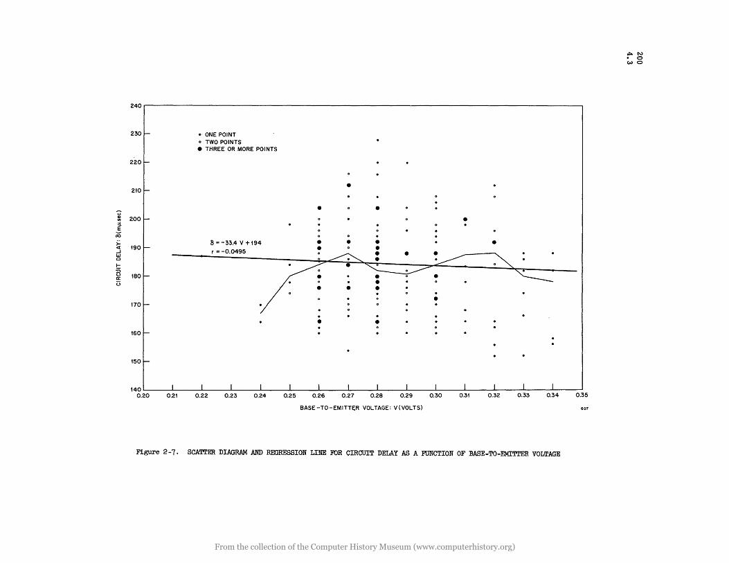
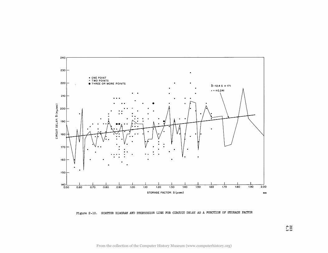
Studies in Regression Analysis. To investigate whether there is any direct relationship between circuit delay (6) and any of the four transistor parameters listed, the measured value of circuit delay for 236 transistors, assuming these to be a representative sample of the population of all GT762 transistors, was plotted against each of the parameters. It was assumed that the regression of 6 on each of the parameters V, ~, T, and S is linear. The scatter diagrams of 6 versus each of the transistor parameters and fitting of linear regression equations are given in figures 2-7 thru 2-10. The mean 8 values are connected in a line of best fit, shown as a light line; the line of regression, shown as a heavy line, is defined as the linear function of the form y = mx + b, which fits the means of arrays best, in the least squares sense. The fitted linear regression equations are given below:
8 = -33.4V + 194 6 -0.08l2~ + 197 6 = 0.577T + 146.5 6 = 12.45 + 171
By using t tests2, it was found that the regression between 8 and V is not statistically significant but the regressions of 6 on the other parameters are highly significant, i.~., at the 1% level. There is a definite indirect relationship, then, among ~, T, Bnd S. The indirect relation-
ships are obtained by using the last three of the above equations. Though the estimated coefficient of regression between 6 and V is greater than the corresponding coefficient between 6 and any other parameter, it is not statistically significant since the estimated variance of this coefficient is very high. Further investigation made to determine whether any direct relationship between the parameters V, ~, T and S existed, indicated a strong direct relationship between both V and T and also between T and ~.
Delay as a Function of Sixteen Expressions. A UNIVAC program was used to find the linear fit and regression coefficients be.tween 6 and the following 16 parameter expressions:
I I 21 2 V, ~, T, S, 1 ~, T ~,T ~,T/~, v/~,
VT, TS, S/~, T2, 1/~2, lis, VS
It was assumed that the coefficients of regression between 6 and other parameter expressions were not significant. The program revealed highest posi-tive regression between 6 and terms T, T2, T2/~, VT. S/~, and TS. These six parameter combinations were chosen for a function with linear constants as follows:
6· KIT + K2T2 + K3VT + K4T2/~
+ KsS/~ + K6TS + K7
(1)
A second program was subsequently written to apply the least-squares fit criterion to the 234 sets of transistor data for the given equation. The normalized equations (seven equations, seven unknowns) of the fit were solved by the Crout Method3• A third program was developed to test the curve fit; that is, to compare the calculated 6 with the observed and to determine the individual term contributions. These programs revealed that the KsS/~and ~ TS terms contributed little to the value and could be dropped, thus simplifying the function to the following:
6 = KIT + K2T2 + K3VT + K4T2/~ + K7' (2)
where Kl - 1.666, K2 = 0.001, K3 = -2.717,
K4 = -0.175, and K7 = 129.135
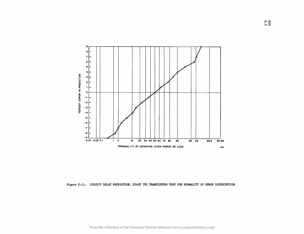
A relatively simple evaluation of the normality of the distribution of errors based on this regression equation is indicated in figure 2-11. The cumulative dis,tribution of errors would appear perfectly linear in the representation of a normally distributed population.
Discussion of Accuracy of Prediction Using the Function. A lot of 99 \ype GT762 transistors from a later shipment was measured to determine the applicability of the derived functions. equations 0) and (2). The distribution of errors between the equation prediction (2) and the observed
From the collection of the Computer History Museum (www.computerhistory.org)
values of delay appeared normal, with a mean of 8%. A change in the constant term or inclusion of dependence on S would correct the function as applied to this particular group and shift the mean to zero.
D. Range Deter.iaation
Since the circuit under design specifies use in one of three delay ranges, rather than a specific delay, a method for classifying transistors into the three ranges according to known parameters would serve the purpose. The method capitalizes on the relationship established in the search for a predictive function.
The 236 units first investigated were plotted on a T-ordinate, ~-abscissa graph, and labeled with their observed a values. Arbitrary 6 ranges were found to separate themselves fairly well into various regions of the plot; rough borders were sketched between regions following the best range separations. These T (~) curves descended exponentially at low ~ values, and leveled off horizontally as ~ increased, suggesting the functional relationship:
-K~ T = Kl + K2e (4)
The a-labeled points were separated into the three designated groups: 0-155 ~s, 156-195 m~s, and 196-234 m~s; and the two borders were added. A program was devised to fit the border ~, T data to the suggested functional expression, yielding the constants Kl , K2, K3 for each curve. The
smooth exponential decay curves were drawn in to separate the data. The results, for the first lot of 234 type GT762 transistors, are described as follows:
1) In the high range (196 < 5 < 235), eight units out of 52 occurred which did not belong. Their values were 180, 180, 186, 192, 192, 192, 192, 194 m~. Thus there were only two outside of the tolerance criterion, ± 10 m~. This tolerance was selected arbitrarily by adding the measurement tolerances of T and 5, each ± 5 m~s.
2) In the medium range (156 S a S 195) nine units out of 179 occurred which did not belong. One unit was below (152), and eight units were above (196, 196, 196, 198, 198, 198, 200, 200). None of these was outside the ~ 10 m~ tolerance region.
3) The low range (a s 155) contained only two units, both of which were correctly placed.
4) The two border equations are as follows:
T = 30.97 + 60.58e-o·0157P at 5 = 155
T = 62.18 + 112.41e-o,OI66~ at 5 = 195
(5)
~)
The results suggest a very accurate separation. The lowest region, where there was insufficient data available, was checked on another set of transistors. The results are discussed below.
Figure 2-12 is a graph that can be used to sort transistors by ~ and T measurements. Once the measurements for each transistor are made, the ~-T point on the graph establishes the delay range of the unit.
Discussion of Accuracy of Prediction Using Ranges Determined. With the method just indicated, using the transistor delay-range chart with the originally derived borders (figure 2-12), the new lot of 99 type GT762 transistors was plotted. There were 28 transistors in the high range (196 ~ 0 ~ 235).
In the medium range (156 ~ 0 ~ 195), 69 units occurred, of which 11 did not belong. Nevertheless, of these 11, ten units were acceptable under the tolerance limits, indicating only one misplaced.
In the low delay range (6 ~ 155), only two transistors occurred, both of which were correctly placed.
A linear shift in the borders of the a ranges wobld take care of the errors of misplacement. These results are strongly indicative that new lots of the transistor have some property changes that can affect our application, unless additional parameters such as storage time (S) are considered.
An excellent prediction for the TA1830 data was achieved by the transistor delay-range chart (figure 2-12). Of the 25 units tested, 22 fell within the predicted range and 3 were borderline. The borderline cases were so close that, within tolerance limits, they could be placed in the correct categories.
In contrast to the broad range of delay values in the original 236 type GT762 transistors, these RCA TAI830 units were mostly confined to the lowest delay range.
Acknowledgements
The authors gratefully acknowledge the assistance of the many groups and departments of Remington Rand Univac who contributed to the success of this paper. Special acknowledgement is given to P. Krishnaiah and P. Steinberg.
References
lEzekiel, Mordecai. Methods of Correlation Analysis. 2nd ed. New York: Wiley, 1941.
2Johnson, P. Research Chap. V.
3nildebrand, Analysis. p. 429.
o. Statistical Methods in Prentice Hall, Inc., 1944.
F. B. Introduction to Numerical McGraw Hill, 1956.
191 4.3
From the collection of the Computer History Museum (www.computerhistory.org)

192 4.3
4Gray, Harry J., Jr. An Application of Piecewise Approximations to Reliability and Statistical Design and Proceedings of IRE. July, 1959.
~emington Rand Univac, Division of Sperry Rand Corporation. Statistical Techniques in Transistor Evaluation Final Report. Dept. of the Navy, Bureau of Ships NObs 72382. Applied Math Department: Remington Rand Univac, Philadelphia, Pa. April, 1959.
6Senner, A. H., and Meredith, B. Designing Reliability into Electronic Circuits. Proc. Nat'l Electronics Conf. Vol. 10, pp 137-145. Oct. 1954.
7Gray, H. J., Jr. An Application of Piecewise Approximations to Reliability and Statistical Design. Proc. of the IRE Vol. 47, No.7, pp. 1226-1231. July, 1957.
8Remington Rand Univac, Division of Sperry Rand Corporation. Univac Larc Highspeed Circuitry Case History in Circuit Optimization. Prywes, N. S., Lukoff, N., and Schwartz, J. Remington Rand Univac, Philadelphia, Pa.
9Remington Rand Univac, Division of Sperry Rand Corporation. The Univac Prepared Engineering Document Program. Williams, T. Remington Rand Univac, Philadelphia, Pa.
l~emington Rand Univac, Division of Sperry Rand Corporation. The Backboard Wiring Problem: A Placement Algorithm. Steinberg, L. Remington Rand Univac, Philadelphia, Pa.
From the collection of the Computer History Museum (www.computerhistory.org)

w ::: to-« (!) IJJ z
v ~ )(
IJJ 0-0 ...J (f)
64 ~--------------------------------------------------------~
56
--~--ACTUAL
THEORETICAL , ,
48 , I I ,
40 , , , ,
I , 32 , ,
P J
24
15 25 35 45 55 65 75 85
TEMPERATURE (OC) 701
Figure 1-1. PUNCH-THROUGH VOLTAGE SLOPE PREDICTION
193 4.3
From the collection of the Computer History Museum (www.computerhistory.org)

12
II
10
9
II)
>u 8 m u> ~ 7 0 >
~ 6 x <!) ::> 0 5 0:: X l-X 0 4 z ::> Q.
3
2
85°C Vp =10.6-58xl0-4 t
25°C Vp =1O.6-0.36xl0-4 t ---- - - ---- --.'-1.TL T2~',';~~ ~~~~~E
"
65°C Vp =10.6-4xl0-4 t
75°C Vp =10.6-28xl0- 4 t
..........
"-
" "
o ~'------------------~ __________ ~ ______ ~~ ______ -L~ __________ ~ ________ -L __ ~ ____ ~ __ ~ ______ ~
100 400 1000 2000 4000 10,000 20,000 40,000 100,000
TIME (IN HOURS) 700-Rl
Figure 1-2. PUNCH-THROUGH VOLTAGE ACCELERATED LIFE TEST
,j:::.. I-' (0
W,j:::..
From the collection of the Computer History Museum (www.computerhistory.org)

INPUT TEST POINT
" D
BASE CONNECTIONS
\ R/
NODE 1
R2
TP
+
""....-----...--...., ./ ...... OUTPUT
,/ TRANSISTOR ...... " TEST / COLLECTOR "
/ CONNECTION \ POINT /
/ NODE3~ I \ \
I I , \ \ \
\ EMITTER I \." CONNECTION /
'- ./ .............. _./
........... _--
/ /
/
\ \ I I I
"-NODE 4
Figure 1-3. SAMPLE CIRCUIT FOR FAULT DIAGNOSIS
-Q
RS -ON
-'--~------------~IS
G
+
4402
a. Diode b. Transistor Base c. Transistor Collector
Figure 1-u. VOLTAGE-CURRENT CHARACTZRISTICS OF A DIODE)
A1~ BASE AND COLLECTOR OF A TRANSISTOR
4103
195 4.3
From the collection of the Computer History Museum (www.computerhistory.org)

196 4.3
0 3:'U .... CI) en cn::t. cnE 0-D:cn u .... <X-
=> ~u ....J~ lLIU 0
80~---------------------------------------------,
75 I-
70 I-
65 I-
~~
0 0
TRANS I STOR /3 = 9 BASE CURRENT 18 = 1.15mo
I I
0.4 0.8
OPTIMUM
1.2
-L Xl03 R3
1.6 I
2.0
Figure 1-5. DELAY AS A FUNCTION OF THE 1/R3
2.4
5634-Rl
From the collection of the Computer History Museum (www.computerhistory.org)

+t2
+0.75
Figure 2-1. SCHEMATIC DIAGRAM OF CIRCUIT
FF +
CLOCK PULSE
MEASURED DELAY
Figure 2 -2. DELAY MEASUREMENT
LOADING CIRCUIT
617
618
197 4.3
From the collection of the Computer History Museum (www.computerhistory.org)

198 4.3
r--i\----I I rV-I I I I
FASTL-J' ________________ ~_+~ ~--~ FF
~L~PC~~~~~;_ -- - --\J I UN DER TEST I I FF I I I I CLOCK I
PULSE
L ______ -~ ~----------8mox.----------~
31 LOADING CIRCUITS
Figure 2-3. INPUT AND LOADING FOR MAXIMUM DELAY
-4.1
MERCURY - RELAY PULSE ~--~~~-+~
GENERATOR
a. Circuit
I- 5fLsec -I
lL...--1t ___ ----I1 b. Input Voltage
O-----~========~~~~~~~-
_4.1---..:::31;.;.;~9::.;'lf~4~-------------------~ ~r:~ c. Output Waveform
620
Figure 2 -4. MEASUREMENT OF RISE TIME
619
From the collection of the Computer History Museum (www.computerhistory.org)

50mJLsec TC r----., MERCURY-RELAY~ : 100Q I Q
PULSE Wv I "NY ._ .. -GENERATOR I I I \.
I 50JLJLf -r- I I -L.. I L ___ ~...J
a. Circuit
I .. _I
-4.1
I' 5~ .. c ., • I b. Input Voltage
\ T c. Output of RC Circuit
d. Bose -to- Emitter Waveform
Figure 2-5. MEASUREMENT OF PEAK BASE VOLTAGE
Vc ~-8V
-v
a. Circuit
Vc ~Ts=E b. Output Voltage
+3V----~--~ __ --__ -
o L
-12V -....,""'--+----__ _
C. Input Voltage at A 622
621
Figure 2 -6. MEASUREMENT OF STORAGE TIME
~~ • (0 (.to) (0
From the collection of the Computer History Museum (www.computerhistory.org)
u Q) In ::l E
ro >-<{ ...I w 0
I-
~ 0: U
240
230 l- e· ONE POINT o TWO POINTS • THREE OR MORE POINTS
220
• 210
• • 200 •
'90~ 8 = -33.4 V + '94 • • • • • r = -0.0495
180
170 I / · • • I
160
150
140 0.20 0.21 0.22 0.23 0.24 0.25 0.26 0.27 0.28 0.29 0.30 0.31 0.32 0.33 0.34
BASE-TO-EMITTE;R VOLTAGE: V(VOLTS)
Figure 2-7. SCATTER DIAGRAM AND ROORESSION LINE FOR CIRCUIT DELAY AS A FUNCTION OF BASE-TO-EMITTER VOLTAGE
0.35
607
~ N
• e we
From the collection of the Computer History Museum (www.computerhistory.org)

'0 Ql
~ E
(.0
;>.: « ....J lLJ 0
l-S (,) a:: (,)
240
230
220
210
200
190
180
170
160
150
• ONE POINT o TWO POINTS
. . 8 = -0.0812 f3 + 197 r = -0.393
140 I !
50 70 90 110 130 150 170 190 210 230 250 270 290 310 330 350
BETA:f3 608
Figure 2 -8. SCATTER DIAGRAM AND REGRESSION LINE FOR CIRCUIT DELAY AS A FUNCTION OF BETA
~N
• 0 w· ......
From the collection of the Computer History Museum (www.computerhistory.org)

240
230
220~ 210
'0 Q)
i 200
5 c:o >-« 190 ...J w 0
I-:; u 180 0: U
170
160
150
• ONE POINT o TWO POINTS • THREE OR MORE POINTS
..
8 = 0.577 T + 146.5 r = 0.7895
140~1 ______ L-____ -L ______ L-____ -L ______ L-____ -L ______ L-____ -L ______ L-____ -L ______ L-____ -L ______ L-____ -L ____ ~
o 10 20 30 40 50 60 70 80 90 100 110 120 130 140 150
TRANSISTOR DELAY: T (mJLsec) 609
Figure 2-9. SCATTER DIAGRAM AND REGRESSION LINE FOR CIRCUIT DELAY AS A FUNCTION OF TRANSISTOR DELAY
.l::>.~ o
eN ~
From the collection of the Computer History Museum (www.computerhistory.org)
240
230
220
210
U Q)
1 200
.5 ro
>-190 <{
....J lLJ 0
!:: ::J u 180 0::
u
170
160
150
140 0.50
• ONE POINT o TWO POINTS • THREE OR MORE POINTS
8=12.45+171
0.90 1.00 1.10 1.20 1.30 1.40 1.50 1.60 1.70 1.80 1.90
STORAGE FACTOR: S (j-Lsec)
Figure 2-10. SCATTER DIAGRAM AND REGRESSION LINE FOR CIRCUIT DELAY AS A FUNCTION OF STORAGE FACTOR
2.00
606
~N • 0 ww
From the collection of the Computer History Museum (www.computerhistory.org)
9
8
7
I-- I l-
6
5
4 z 52 3 I-(,)
0 2 lIJ 0:: Cl.
~ 0 0:: 0 0:: -t 0:: lIJ
I- -2 z lIJ -3 (,) 0:: lIJ Cl. -4
-5
-6
-7
-8
I-- l) I-- / I--
V I-
'- V - V
./ -- // - v/ --- v -
I
l-
I- /1) (
-9 -O.Ot 0.050.t 2 to 20 30 40 50 60 70 80 90 98 ' 99 99.9 99.99
PROBABILITY OF OBTAINING GIVEN ER,ROR OR LESS 610
Figure 2-11. CIRCUIT DELAY PREDICTION, 234GT 762 TRANSISTORS TEST FOR NORMALITY OF ERROR DISTRIBUTION
tIl-N • 0 Wtll-
From the collection of the Computer History Museum (www.computerhistory.org)

U Q)
'" :t.. E j::'
w ::E ~ w en ii: a:: 0 I-en en z « a:: I-
120
flO
100 \ "l.
90
80
70
~ CD --"'\.
~ CIRCU IT DELAY RANGE:
196-235mJLsec
~ r-,... t::::L --r...- r---a...--
60
50
40
~h ® --
~ ~
CIRCUIT DELAY RANGE: 156-195mJLsec
h "-
~ 1"1-IL---,
30 0 --
CIRCUIT DELAY RANGE: 0-155mJLsec
I I o 50 70 90 110 130 150 170 190 210 230
f3 (CURRENT GAIN)
Figure 2-]2. CIRCUIT DELAY RANGES
250 270 290 310 330 350
605-R'
~N • 0 w C11
From the collection of the Computer History Museum (www.computerhistory.org)

From the collection of the Computer History Museum (www.computerhistory.org)