Embed Size (px)
Citation preview
CMU ECE347 – Fall 2002 Lec.12 - 1
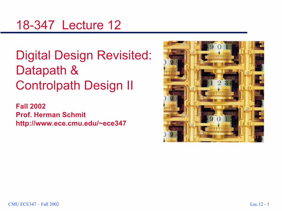
18-347 Lecture 12
Digital Design Revisited: Datapath & Controlpath Design IIFall 2002Prof. Herman Schmithttp://www.ece.cmu.edu/~ece347
CMU ECE347 – Fall 2002 Lec.12 - 2
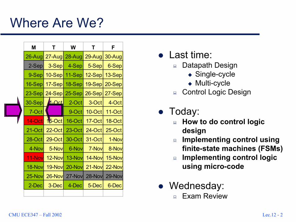
Where Are We?
M T W T F26-Aug 27-Aug 28-Aug 29-Aug 30-Aug
2-Sep 3-Sep 4-Sep 5-Sep 6-Sep
9-Sep 10-Sep 11-Sep 12-Sep 13-Sep
16-Sep 17-Sep 18-Sep 19-Sep 20-Sep
23-Sep 24-Sep 25-Sep 26-Sep 27-Sep
30-Sep 1-Oct 2-Oct 3-Oct 4-Oct
7-Oct 8-Oct 9-Oct 10-Oct 11-Oct
14-Oct 15-Oct 16-Oct 17-Oct 18-Oct
21-Oct 22-Oct 23-Oct 24-Oct 25-Oct
28-Oct 29-Oct 30-Oct 31-Oct 1-Nov
4-Nov 5-Nov 6-Nov 7-Nov 8-Nov
11-Nov 12-Nov 13-Nov 14-Nov 15-Nov
18-Nov 19-Nov 20-Nov 21-Nov 22-Nov
25-Nov 26-Nov 27-Nov 28-Nov 29-Nov
2-Dec 3-Dec 4-Dec 5-Dec 6-Dec
Last time: Datapath Design
Single-cycleMulti-cycle
Control Logic Design
Today:How to do control logic designImplementing control using finite-state machines (FSMs)Implementing control logic using micro-code
Wednesday:Exam Review

CMU ECE347 – Fall 2002 Lec.12 - 3
Today’s Menu
Datapath - some examplesHow datapaths appear in real chipsWhy is it difficult to design them
Control logicHow control logic appears in real chips
Implementing control logic using finite-state machines (FSMs)Mealy vs. Moore FSMs – revisited
Implementing control logic using micro-code
Logic synthesis!
CMU ECE347 – Fall 2002 Lec.12 - 4
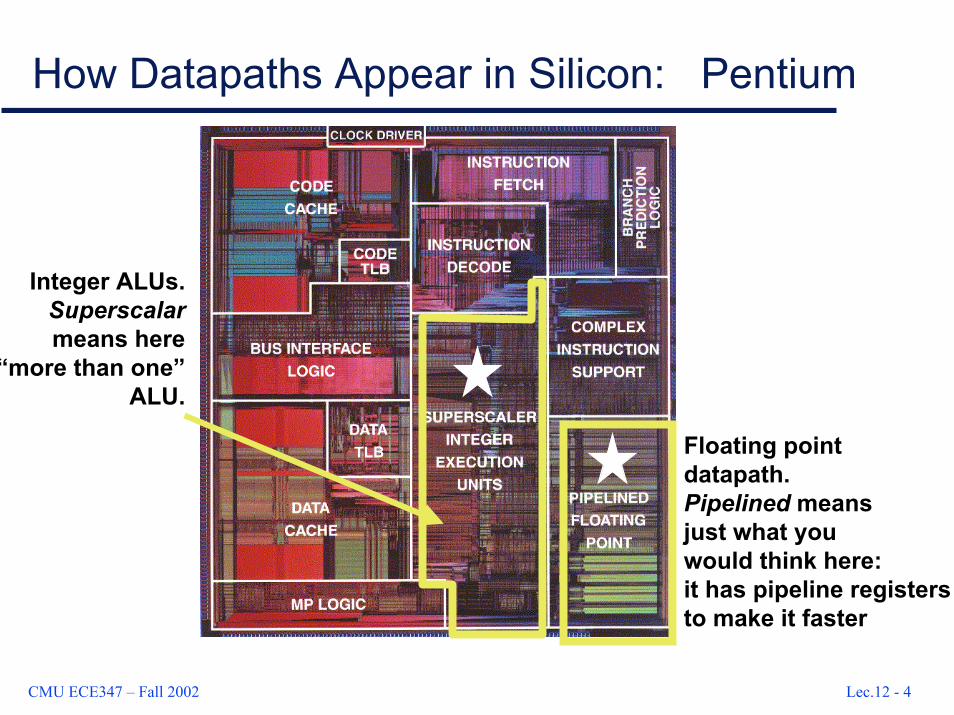
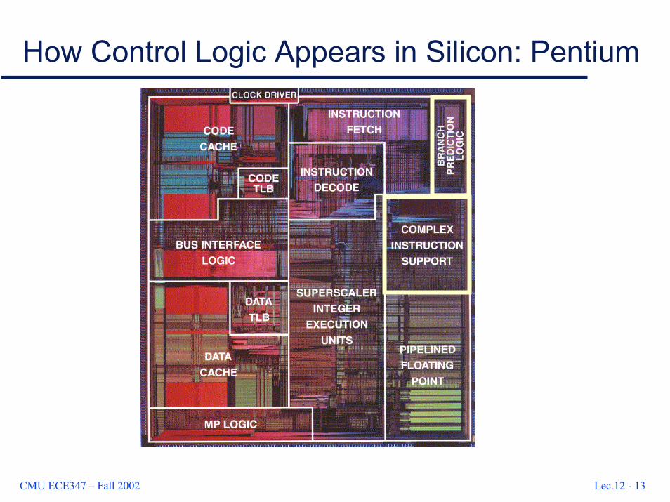
How Datapaths Appear in Silicon: Pentium
Integer ALUs.Superscalarmeans here
“more than one”ALU.
Floating pointdatapath.Pipelined meansjust what youwould think here:it has pipeline registersto make it faster
CMU ECE347 – Fall 2002 Lec.12 - 5
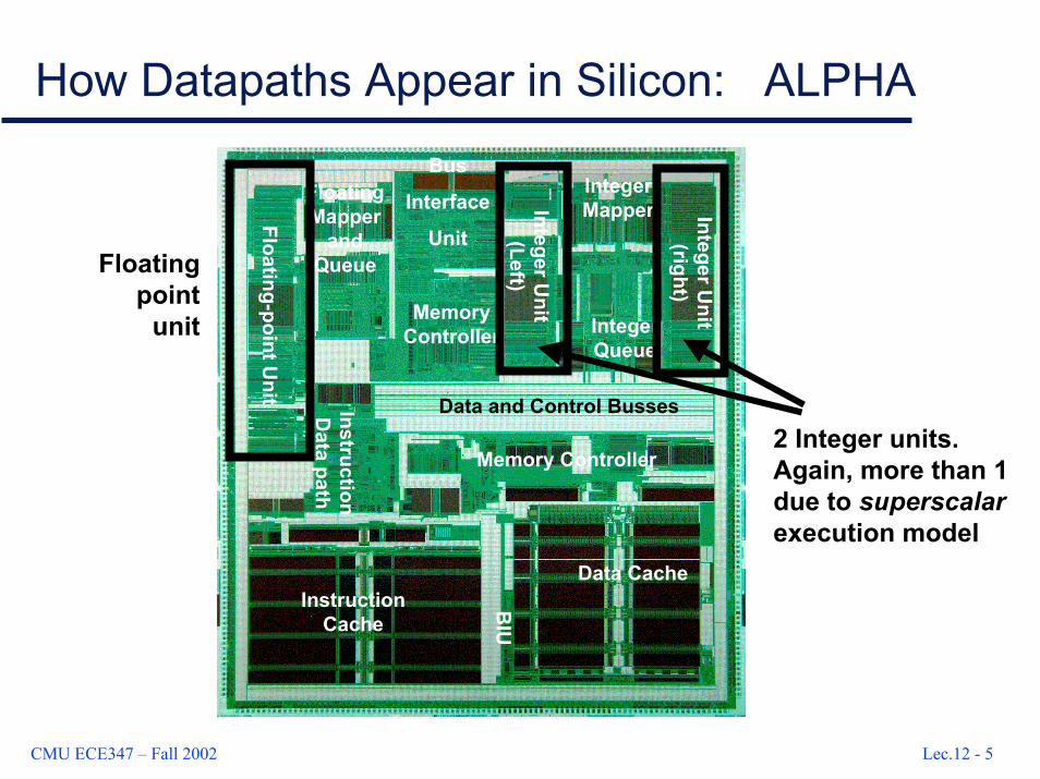
How Datapaths Appear in Silicon: ALPHA
Instruction Cache
Data Cache
Data and Control Busses
Integer Mapper
Integer Queue
Integer Unit
(right)
Integer Unit
(Left)
Memory Controller
Bus
Interface
Unit
Floating-point Unit
Floating Mapper
and Queue
Memory Controller
Instruction D
ata path
BIU
2 Integer units.Again, more than 1due to superscalarexecution model
Floatingpoint
unit
CMU ECE347 – Fall 2002 Lec.12 - 6
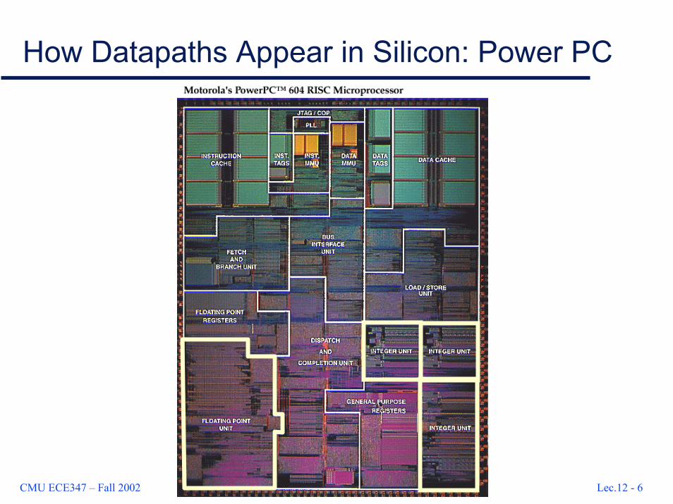
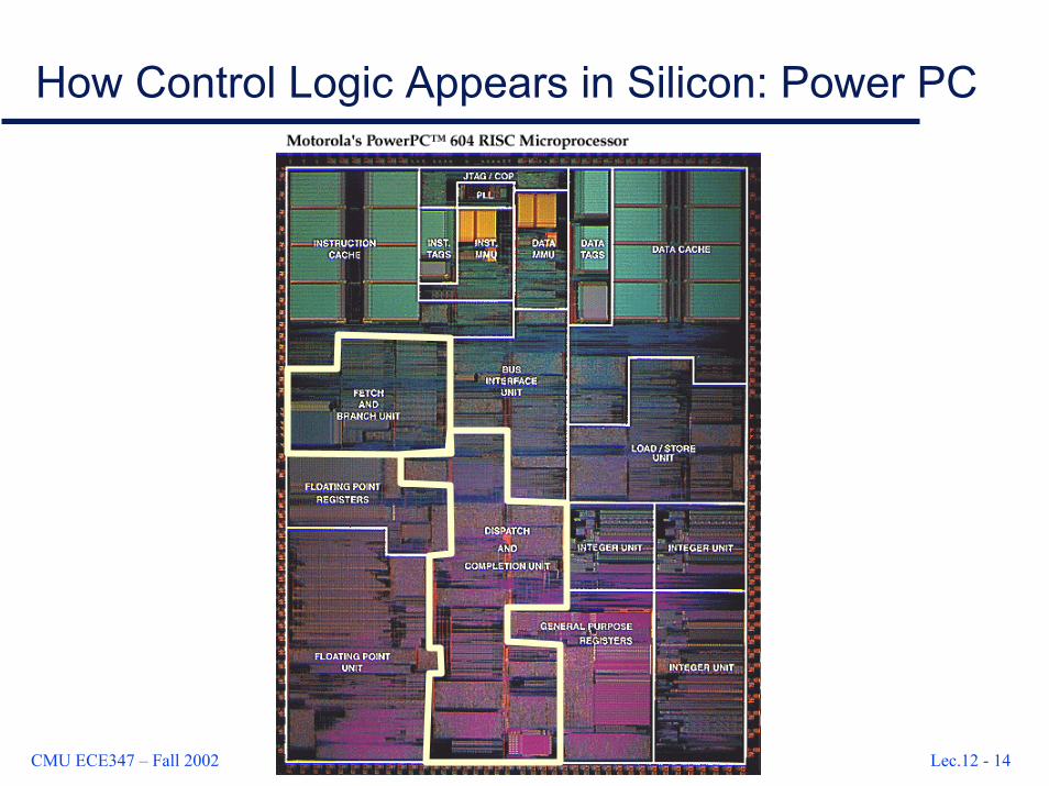
How Datapaths Appear in Silicon: Power PC
CMU ECE347 – Fall 2002 Lec.12 - 7
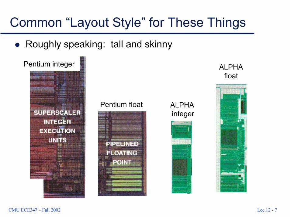
Common “Layout Style” for These ThingsRoughly speaking: tall and skinny
Pentium integer ALPHAfloat
Pentium float ALPHAinteger
CMU ECE347 – Fall 2002 Lec.12 - 8
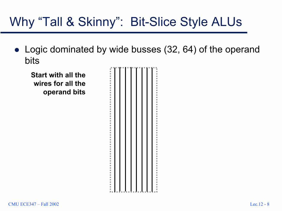
Why “Tall & Skinny”: Bit-Slice Style ALUs
Logic dominated by wide busses (32, 64) of the operand bits
Start with all thewires for all the
operand bits
CMU ECE347 – Fall 2002 Lec.12 - 9
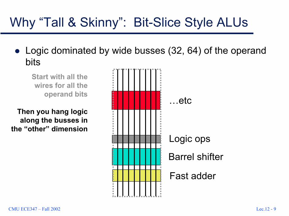
Why “Tall & Skinny”: Bit-Slice Style ALUs
Logic dominated by wide busses (32, 64) of the operand bits
Start with all thewires for all the
operand bits
Then you hang logicalong the busses in
the “other” dimension
…etc
Logic ops
Barrel shifter
Fast adder
CMU ECE347 – Fall 2002 Lec.12 - 10
Why “Tall & Skinny”: Bit-Slice Style ALUs
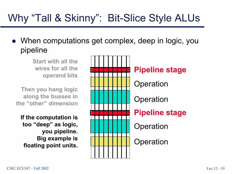
When computations get complex, deep in logic, you pipeline
Start with all thewires for all the
operand bits
Then you hang logicalong the busses in
the “other” dimension
If the computation istoo “deep” as logic,
you pipeline.Big example is
floating point units.
Pipeline stage
Operation
Operation
Pipeline stage
Operation
Operation
CMU ECE347 – Fall 2002 Lec.12 - 11
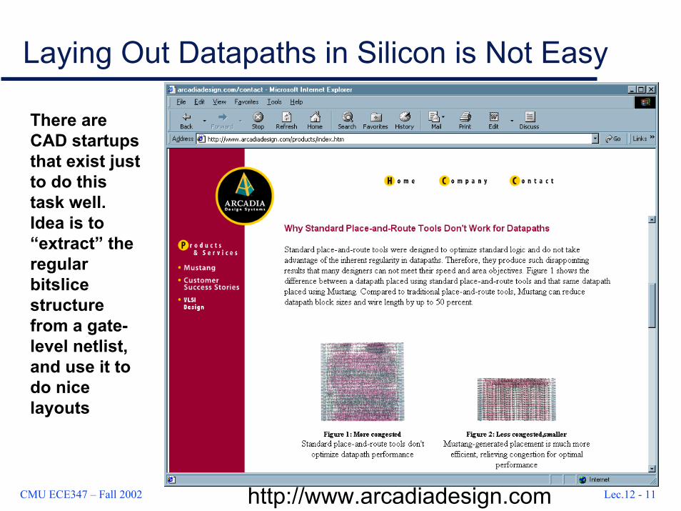
Laying Out Datapaths in Silicon is Not Easy
http://www.arcadiadesign.com
There areCAD startups that exist just to do this task well. Idea is to “extract” the regular bitslice structure from a gate-level netlist, and use it to do nice layouts
CMU ECE347 – Fall 2002 Lec.12 - 12
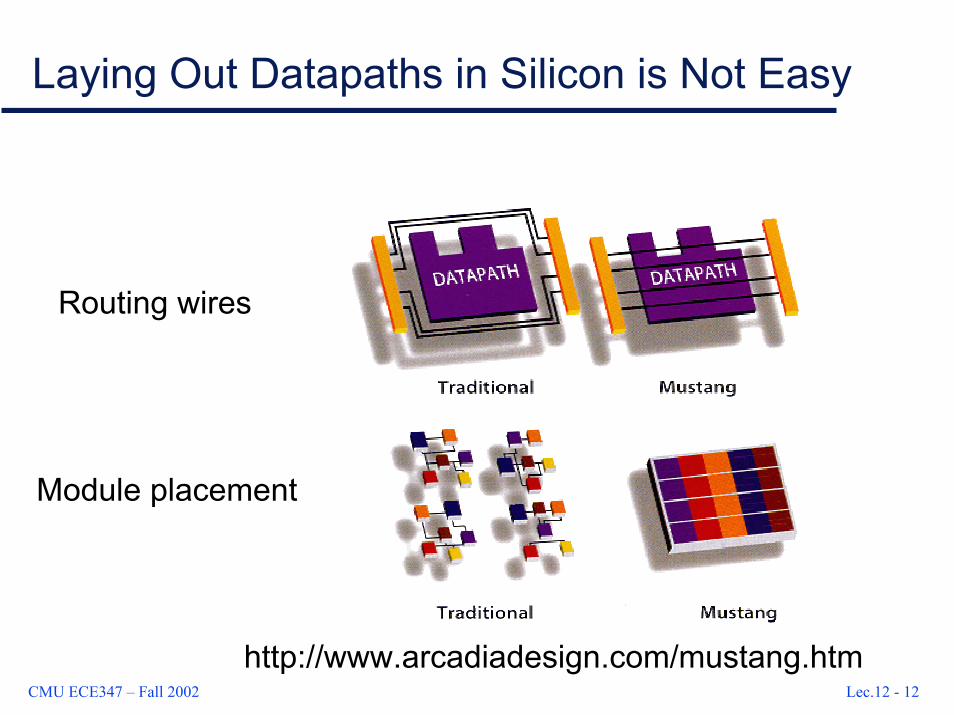
Laying Out Datapaths in Silicon is Not Easy
Routing wires
Module placement
http://www.arcadiadesign.com/mustang.htm
CMU ECE347 – Fall 2002 Lec.12 - 13
How Control Logic Appears in Silicon: Pentium
CMU ECE347 – Fall 2002 Lec.12 - 14
How Control Logic Appears in Silicon: Power PC
CMU ECE347 – Fall 2002 Lec.12 - 15
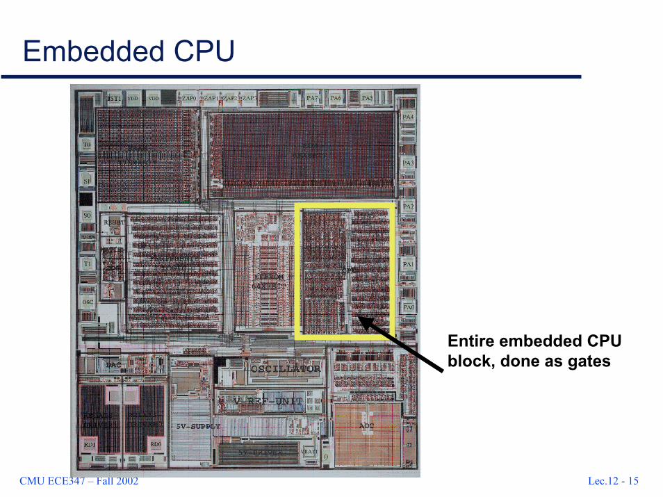
Embedded CPU
Entire embedded CPUblock, done as gates
CMU ECE347 – Fall 2002 Lec.12 - 16
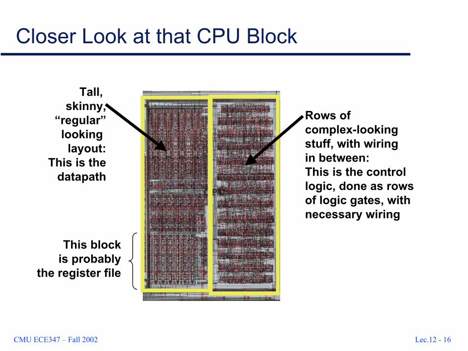
Closer Look at that CPU Block
Tall, skinny,
“regular”looking
layout:This is the
datapath
Rows ofcomplex-lookingstuff, with wiringin between:This is the controllogic, done as rowsof logic gates, withnecessary wiring
This blockis probably
the register file
CMU ECE347 – Fall 2002 Lec.12 - 17
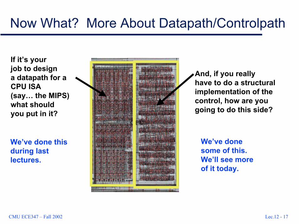
Now What? More About Datapath/Controlpath
If it’s yourjob to designa datapath for a CPU ISA(say… the MIPS)what shouldyou put in it?
And, if you reallyhave to do a structuralimplementation of thecontrol, how are yougoing to do this side?
We’ve done some of this. We’ll see more of it today.
We’ve done this during last lectures.
CMU ECE347 – Fall 2002 Lec.12 - 18
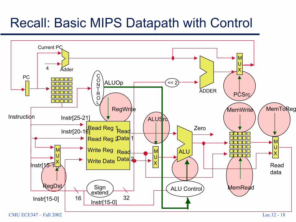
Recall: Basic MIPS Datapath with Control
Read Reg 1
Read Reg 2
Write Reg
Write Data
ReadData 1
ReadData 2
RegWrite
ALU
Instruction
Signextend
16 32
Read data
MUX
MUX
Instr[25-21]
Instr[20-16]
Instr[15-11]
Instr[15-0] Instr[15-0]
ALU Control
ALUSrc
PCSrc
MemToReg
MemRead
MUX
RegDst
PCAdder4
Current PC
ADDER<< 2
MUX
MemWrite
CONTROL
ALUOp
Zero
CMU ECE347 – Fall 2002 Lec.12 - 19
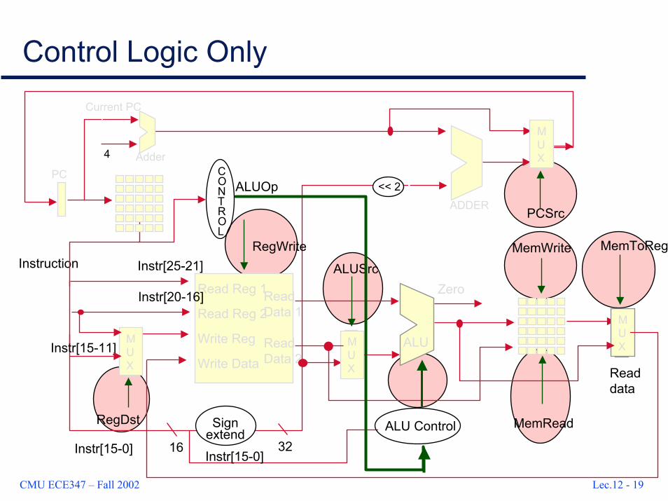
Control Logic Only
Read Reg 1
Read Reg 2
Write Reg
Write Data
ReadData 1
ReadData 2
RegWrite
ALU
Instruction
Signextend
16 32
Read data
MUX
MUX
Instr[25-21]
Instr[20-16]
Instr[15-11]
Instr[15-0] Instr[15-0]
ALU Control
ALUSrc
PCSrc
MemToReg
MemRead
MUX
RegDst
PCAdder4
Current PC
ADDER<< 2
MUX
MemWrite
CONTROL
ALUOp
Zero
CMU ECE347 – Fall 2002 Lec.12 - 20
Control Logic Implementation
How do we generate control signals?Basic logic synthesis stuff
Take the opcode, function bitsProduce control signals for all MUXes, registers, memory modules, ALUs, adders, etc.
We have seen how we generate control signals for the ALU operations
Single cycle Implementation:Assumes everything happens during a single clock cycleInput: instructionOutput: one wide “word” of control
Multi-cycle implementation:Control signals have to be enabled/disabled on a per-cycle basisJust using combinational logic for generating control signals won’t work
CMU ECE347 – Fall 2002 Lec.12 - 21
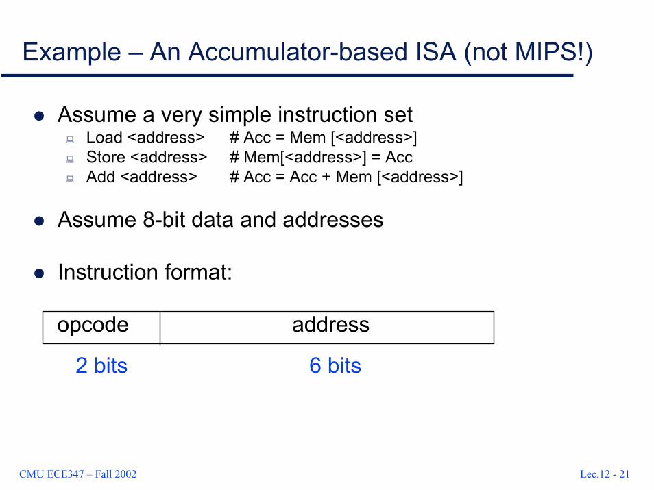
Example – An Accumulator-based ISA (not MIPS!)
Assume a very simple instruction setLoad <address> # Acc = Mem [<address>]Store <address> # Mem[<address>] = AccAdd <address> # Acc = Acc + Mem [<address>]
Assume 8-bit data and addresses
Instruction format:
opcode address
2 bits 6 bits
CMU ECE347 – Fall 2002 Lec.12 - 22
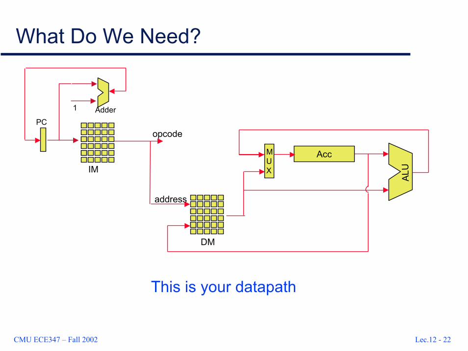
What Do We Need?
PCAdder1
IM
ALU
AccMUX
DM
address
opcode
This is your datapath
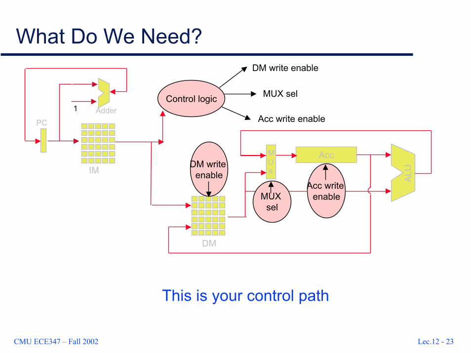
CMU ECE347 – Fall 2002 Lec.12 - 23
What Do We Need?
PCAdder1
IM
DM
ALU
AccMUX
Acc write enableMUX
sel
DM write enable
Control logic
DM write enable
MUX sel
Acc write enable
This is your control path
CMU ECE347 – Fall 2002 Lec.12 - 24
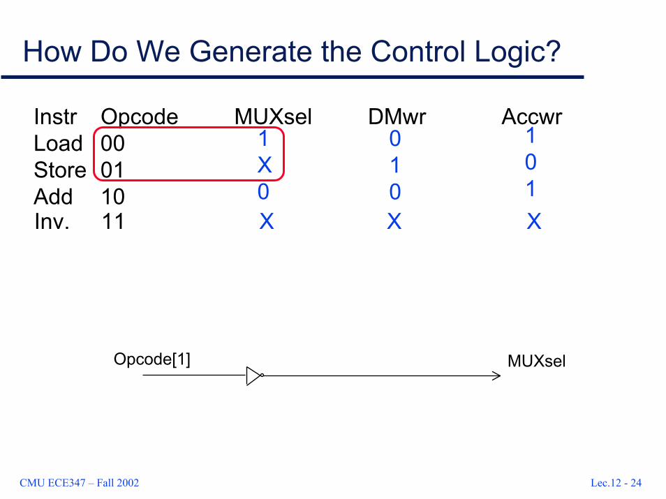
How Do We Generate the Control Logic?
Instr Opcode MUXsel DMwr AccwrLoad 00Store 01Add 10
1X0
010
101
Inv. 11 X X X
MUXselOpcode[1]
CMU ECE347 – Fall 2002 Lec.12 - 25
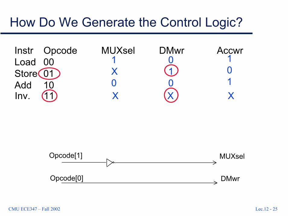
How Do We Generate the Control Logic?
Instr Opcode MUXsel DMwr AccwrLoad 00Store 01Add 10
1X0
010
101
Inv. 11 X X X
MUXselOpcode[1]
Opcode[0] DMwr
CMU ECE347 – Fall 2002 Lec.12 - 26
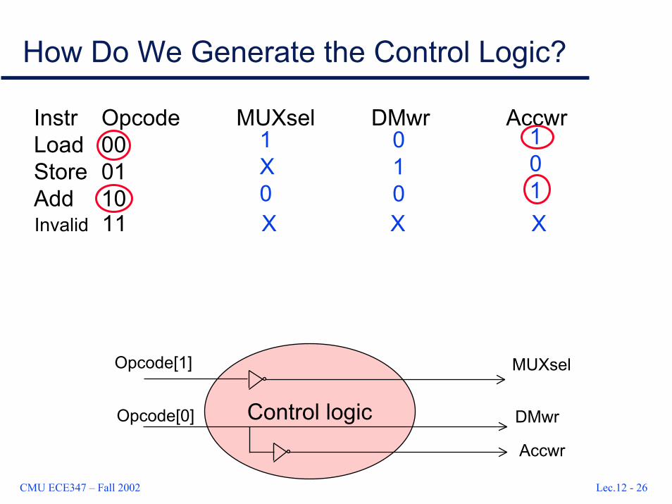
How Do We Generate the Control Logic?
Control logic
Instr Opcode MUXsel DMwr AccwrLoad 00Store 01Add 10
1X0
010
101
Invalid 11 X X X
MUXselOpcode[1]
Opcode[0] DMwr
Accwr
CMU ECE347 – Fall 2002 Lec.12 - 27
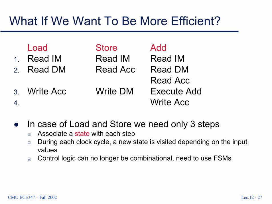
What If We Want To Be More Efficient?
Load Store Add1. Read IM Read IM Read IM2. Read DM Read Acc Read DM
Read Acc3. Write Acc Write DM Execute Add4. Write Acc
In case of Load and Store we need only 3 stepsAssociate a state with each stepDuring each clock cycle, a new state is visited depending on the input valuesControl logic can no longer be combinational, need to use FSMs
CMU ECE347 – Fall 2002 Lec.12 - 28
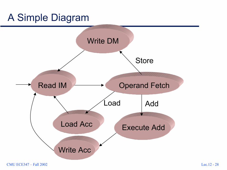
A Simple Diagram
Operand Fetch
Load Acc
Load Add
Write Acc
Execute Add
Read IM
Write DM
Store
CMU ECE347 – Fall 2002 Lec.12 - 29
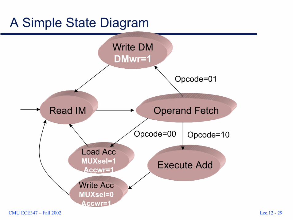
A Simple State Diagram
Operand Fetch
Load AccMUXsel=1Accwr=1
Opcode=00 Opcode=10
Write AccMUXsel=0Accwr=1
Execute Add
Read IM
Write DMDMwr=1
Opcode=01

CMU ECE347 – Fall 2002 Lec.12 - 30
What Kind of FSM is This?
CMU ECE347 – Fall 2002 Lec.12 - 31
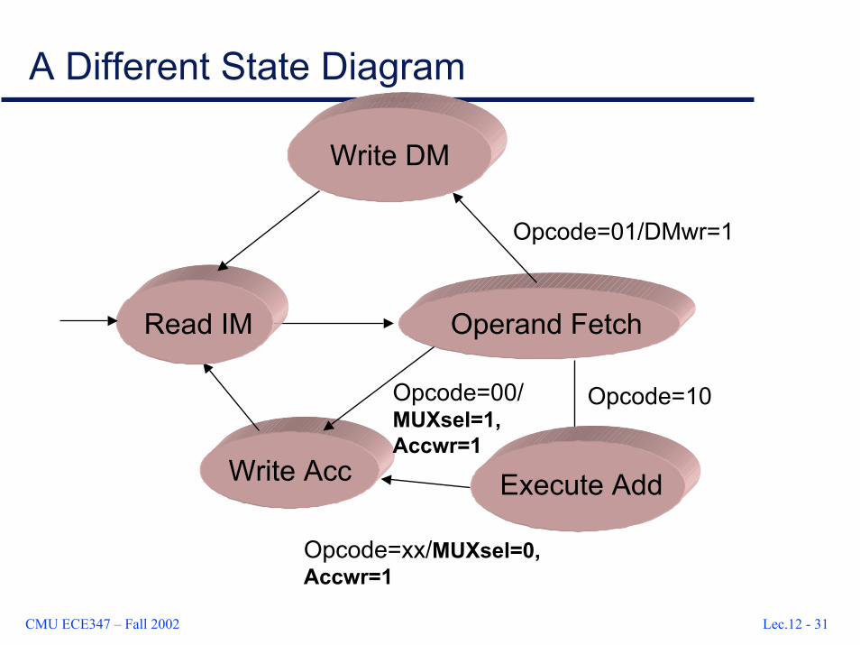
A Different State Diagram
Operand Fetch
Write Acc
Opcode=00/MUXsel=1,Accwr=1
Read IM
Write DM
Opcode=01/DMwr=1
Opcode=10
Execute Add
Opcode=xx/MUXsel=0,Accwr=1
CMU ECE347 – Fall 2002 Lec.12 - 32
What Kind of FSM is This?
CMU ECE347 – Fall 2002 Lec.12 - 33
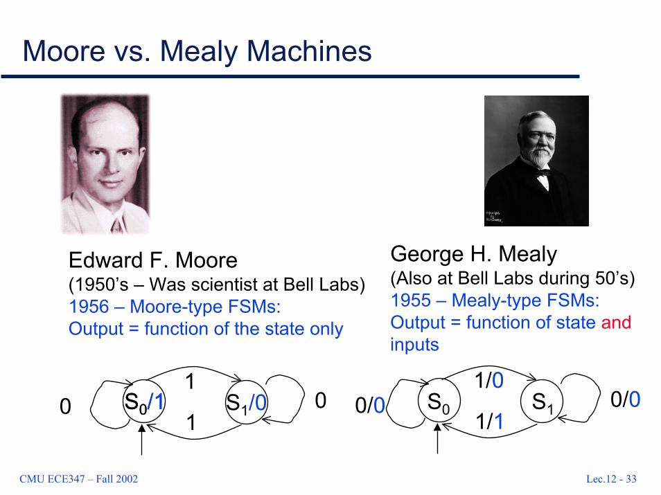
Moore vs. Mealy Machines
George H. Mealy(Also at Bell Labs during 50’s)1955 – Mealy-type FSMs:Output = function of state andinputs
1/0
1/10/0 0/0S0 S1
??Edward F. Moore(1950’s – Was scientist at Bell Labs)1956 – Moore-type FSMs:Output = function of the state only
1
10 0S0/1 S1/0S0/1
CMU ECE347 – Fall 2002 Lec.12 - 34
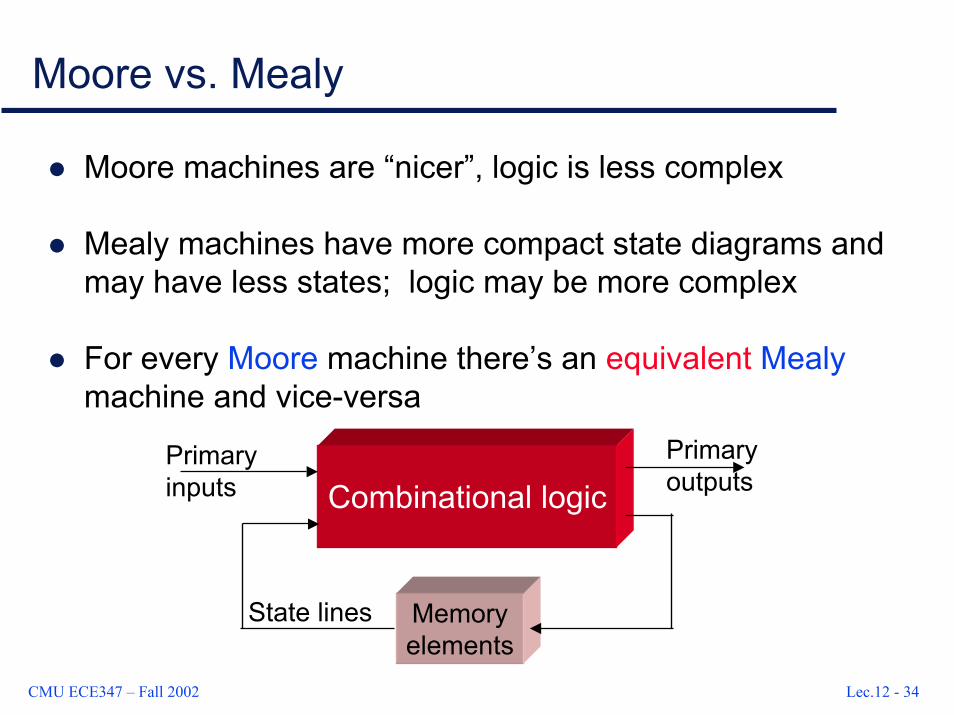
Moore vs. Mealy
Moore machines are “nicer”, logic is less complex
Mealy machines have more compact state diagrams and may have less states; logic may be more complex
For every Moore machine there’s an equivalent Mealymachine and vice-versa
Combinational logic
Memoryelements
State lines
Primaryinputs
Primaryoutputs

CMU ECE347 – Fall 2002 Lec.12 - 35
Microcode: Another Approach
Another way to implement a Mealy machine:
N: Inputs
X: Outputs
S: State Bits
Storage:
X + S (bits/word)
2N+S (words)
Inputs
ROM
Outputs
CMU ECE347 – Fall 2002 Lec.12 - 36
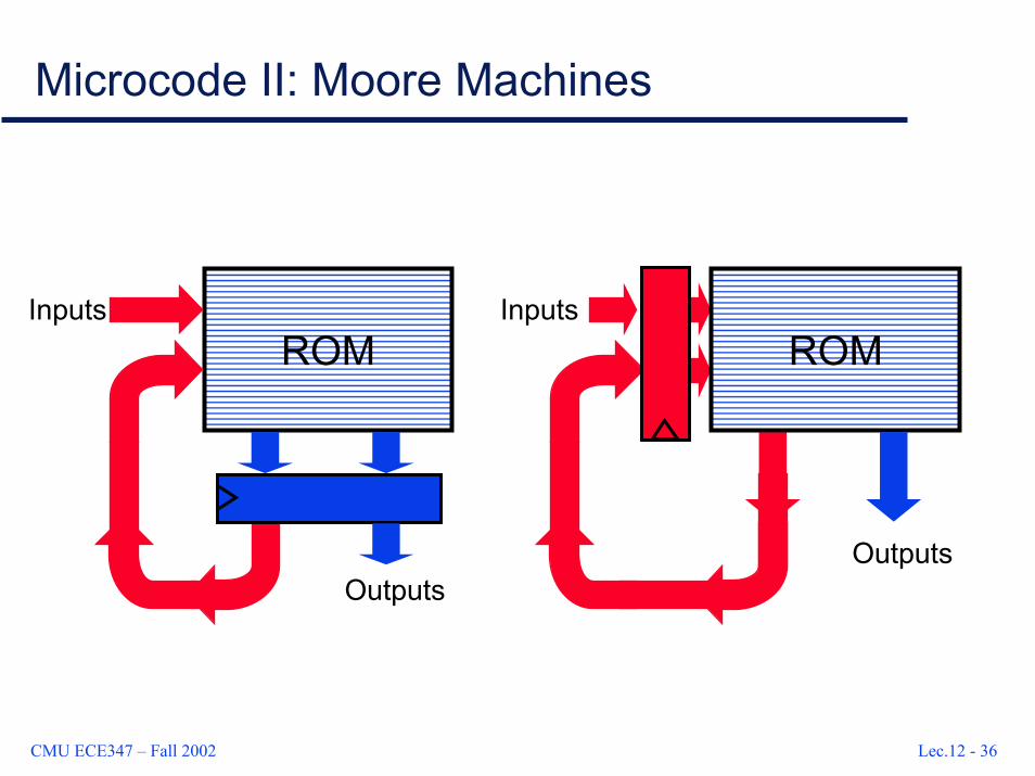
Microcode II: Moore Machines
ROMInputs
Outputs
InputsROM
Outputs
CMU ECE347 – Fall 2002 Lec.12 - 37
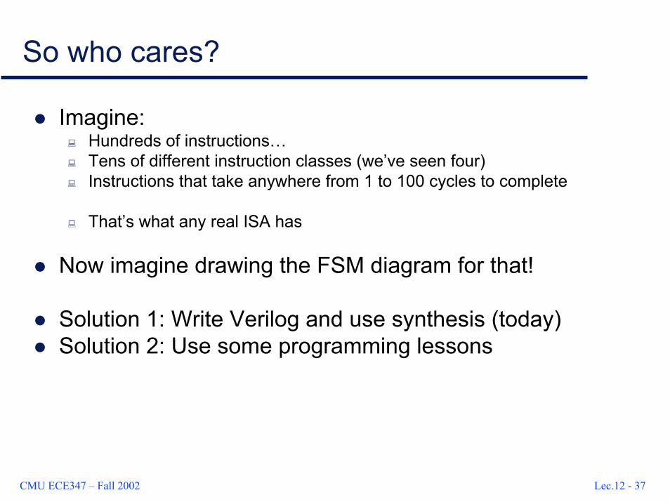
So who cares?
Imagine:Hundreds of instructions…Tens of different instruction classes (we’ve seen four)Instructions that take anywhere from 1 to 100 cycles to complete
That’s what any real ISA has
Now imagine drawing the FSM diagram for that!
Solution 1: Write Verilog and use synthesis (today)Solution 2: Use some programming lessons

CMU ECE347 – Fall 2002 Lec.12 - 38
FSM structureClass 1:
…
Class 2:
……
Class N:
…
Fetch Decode
First cycles are the sameNo reconvergence after decodeLimited Branching
CMU ECE347 – Fall 2002 Lec.12 - 39
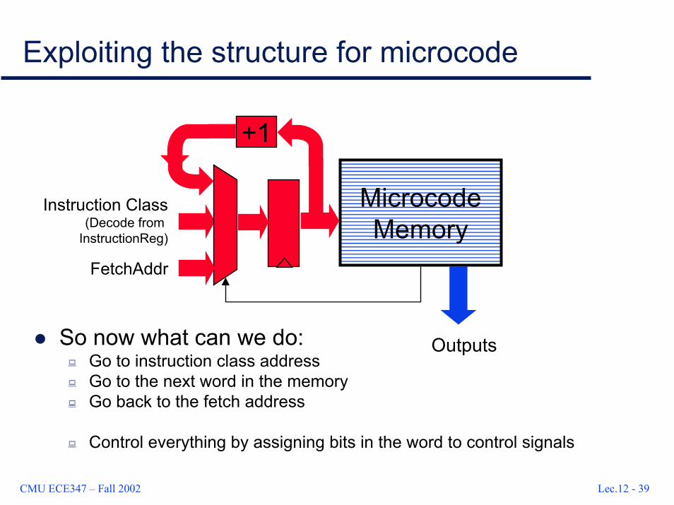
Exploiting the structure for microcode
MicrocodeMemory
Instruction Class(Decode from
InstructionReg)
+1
FetchAddr
So now what can we do:Go to instruction class addressGo to the next word in the memoryGo back to the fetch address
Control everything by assigning bits in the word to control signals
Outputs
CMU ECE347 – Fall 2002 Lec.12 - 40
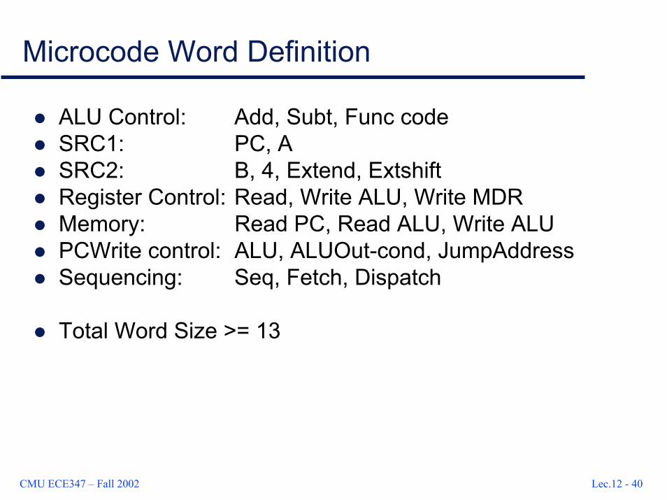
Microcode Word Definition
ALU Control: Add, Subt, Func codeSRC1: PC, ASRC2: B, 4, Extend, ExtshiftRegister Control: Read, Write ALU, Write MDRMemory: Read PC, Read ALU, Write ALUPCWrite control: ALU, ALUOut-cond, JumpAddressSequencing: Seq, Fetch, Dispatch
Total Word Size >= 13
CMU ECE347 – Fall 2002 Lec.12 - 41
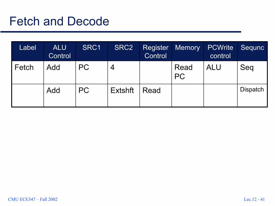
Fetch and Decode
DispatchReadExtshftPC Add
SeqALURead PC
4PCAddFetch
SequncPCWrite control
MemoryRegister Control
SRC2SRC1ALUControl
Label
CMU ECE347 – Fall 2002 Lec.12 - 42
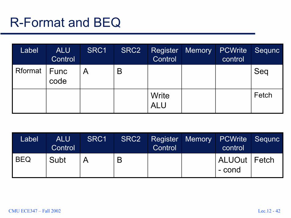
R-Format and BEQ
FetchWrite ALU
SeqBAFunc code
Rformat
SequncPCWrite control
MemoryRegister Control
SRC2SRC1ALUControl
Label
FetchALUOut- cond
BASubtBEQ
SequncPCWrite control
MemoryRegister Control
SRC2SRC1ALUControl
Label
CMU ECE347 – Fall 2002 Lec.12 - 43
Why is this nice?
Reduce complexity of control designOnly way to do it before synthesis toolsOnly way to encode Complex Instruction Sets
Allows bug fixes, optimizations after real hardware
Now how do people do this today?How will we do it for the last stage of the project?
SynthesisSpecify Style for:
RegistersLatchesCombinational LogicFinite State Machines
CMU ECE347 – Fall 2002 Lec.12 - 44
Summary
DatapathUsually regularThe instruction set determines the datapath modules neededMake sure you have all needed modules (e.g., ALUs for doing arithmetic-logic operations, registers to store intermediate results, etc.)
ControlpathNot as regularFor multi-cycle machines, has to be implemented as sequential circuitsMoore vs. Mealy – Moore are easier/nicer to implement, Mealy may have less states, but more complex logicMicrocode – Easier for human design, fixable after fabricationsSynthesis – Specifying Registers, Logic, FSMs
CMU ECE347 – Fall 2002 Lec.12 - 45
Appendix – Moore vs. Mealy FSM
Moore machine: Assume the following encoding
Read IM 000Operand Fetch 001Execute Add 100Load Acc 011Write Acc 010Write DM 101Invalid 11X
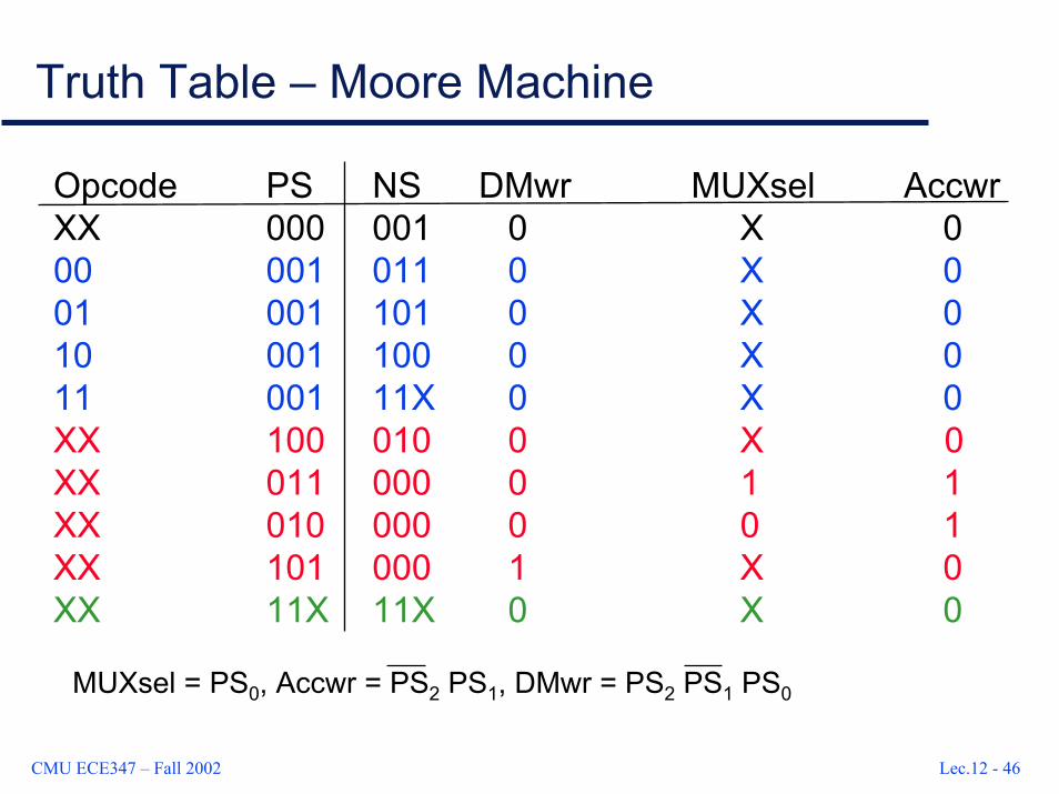
CMU ECE347 – Fall 2002 Lec.12 - 46
Truth Table – Moore Machine
Opcode PS NS DMwr MUXsel AccwrXX 000 001 0 X 000 001 011 0 X 001 001 101 0 X 010 001 100 0 X 011 001 11X 0 X 0XX 100 010 0 X 0XX 011 000 0 1 1XX 010 000 0 0 1XX 101 000 1 X 0XX 11X 11X 0 X 0
MUXsel = PS0, Accwr = PS2 PS1, DMwr = PS2 PS1 PS0
CMU ECE347 – Fall 2002 Lec.12 - 47
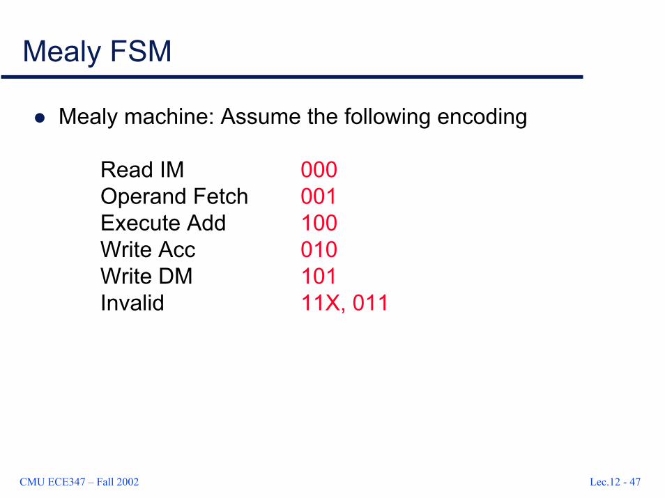
Mealy FSM
Mealy machine: Assume the following encoding
Read IM 000Operand Fetch 001Execute Add 100Write Acc 010Write DM 101Invalid 11X, 011

CMU ECE347 – Fall 2002 Lec.12 - 48
Truth Table – Mealy Machine
Opcode PS NS DMwr MUXsel AccwrXX 000 001 0 X 000 001 010 0 1 101 001 101 1 X 010 001 100 0 X 011 001 11X 0 X 0XX 100 010 0 0 1XX 010 000 0 X 0XX 101 000 0 X 0XX 011 11X 0 X 0XX 11X 11X 0 X 0
MUXsel = PS2 PS1, Accwr = Opcode1 Opcode0 PS2 PS1 PS0 + PS2 PS1 PS0 , DMwr = Opcode1 Opcode0 PS2 PS1 PS0