Embed Size (px)
DESCRIPTION
dfsdf
Citation preview

International Journal of Advances in Engineering & Technology, Sept 2012.
©IJAET ISSN: 2231-1963
156 Vol. 4, Issue 2, pp. 156-166
DESIGN AND LAYOUT OF A ROBUST LOW-POWER SELF-
TIMED SRAM AT 180NM
HaripalKochhar1, Subodh Kansal
2 and Sharmelee Thangjam
3
1 University Institute of Engineering & Technology, Panjab University, Chandigarh, India
2Institute of Engineering & Technology, Bhaddal, Ropar, Punjab, India
3 Asst. Prof., University Institute of Engineering & Technology,
Panjab University, Chandigarh, India
ABSTRACT
SRAM design is very crucial since it takes a large fraction of total power and die area in high-performance
processors. The performance of embedded memory and its peripheral circuits can adversely affect the speed
and power of the overall system. This paper explores the design of SRAM focusing on optimizing delay,
reducing power and layout area. A full-custom layout is drawn to achieve minimum area and power. The key to
low power operation of the design is self-timed architecture, multi stage decodingand full custom layout. The
robustness of this design is verified by analysing the memory at wide PVT range. This memory is verified at a
temperature range of -40ºC to 125ºC.A 1024x16 SRAM is designed at UMC 180 nm technology. The post-layout
behavior of this SRAM is analyzed at different PVT conditions. The dynamic power achieved is 19.74uW at
1MHz frequency at TT_1v_25C. The leakage current of single 6T bit-cell is 4.02pA at TT_1v_25C. The leakage
power is 53.57nW at TT_1v_25C. The access time obtained is 5ns at TT_1v_25C.
KEYWORDS: Low power SRAM, Self-timed, PVT conditions, Full-custom layout, 180nm
I. INTRODUCTION
Low-power SRAM has become more important due to the high demands on the handheld devices. The
active power of the SRAM is mainly consumed in bit lines and data lines because the SRAM charges
and discharges the high capacitive bit lines and data lines in read and write cycles[1]. As the bit width
of SRAM becomes larger for high-performance applications, the power consumption in bit lines and
data lines continues to increase.
Therefore, power dissipation has become an important consideration both due to the increased
integration and operating speeds, as well as due to the explosive growth of battery operated appliances.
Considerable attention has been paid to the low-power and high-performance design.
To reduce the power consumption the first technique is to reduce the active duty cycle of the memory
operation using self-timed architecture. An internal clock pulse with reduced Ton(On time) is generated
which controls all the memory operation. Second technique of power reduction is to use multi-stage
row and column decoding which reduces the power consumption as well as it also improves the timing
characteristics of memory.The behavior of an SRAM differs considerably under different
operatingconditions i.e. PVT conditions. This paper explorers the behavior of SRAM at different PVT
conditions. The range of PVT conditions is:
Temperature : -40ºC – 85ºC
Process Corner : SS, TT, FF
Voltage : 0.9V – 1.98V
International Journal of Advances in Engineering & Technology, Sept 2012.
©IJAET ISSN: 2231-1963
157 Vol. 4, Issue 2, pp. 156-166
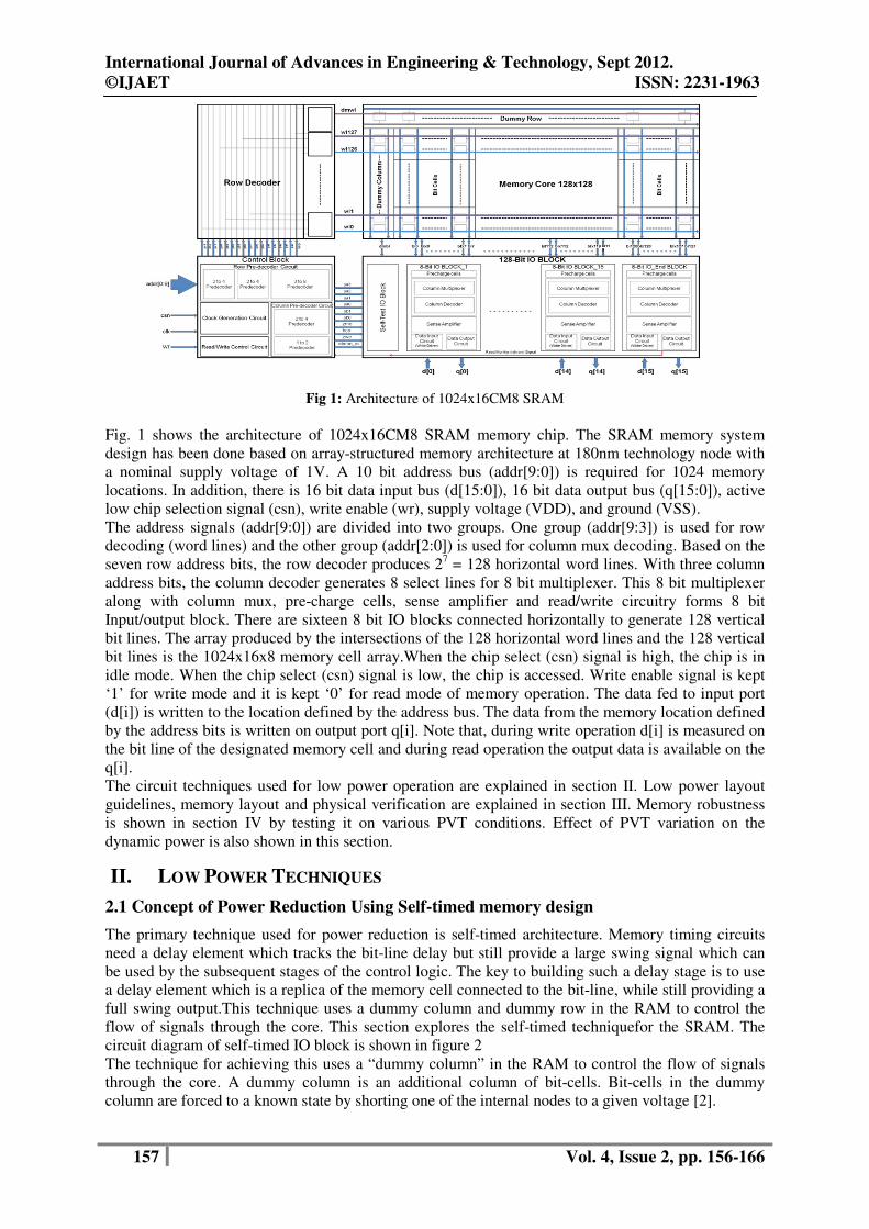
Fig 1: Architecture of 1024x16CM8 SRAM
Fig. 1 shows the architecture of 1024x16CM8 SRAM memory chip. The SRAM memory system
design has been done based on array-structured memory architecture at 180nm technology node with
a nominal supply voltage of 1V. A 10 bit address bus (addr[9:0]) is required for 1024 memory
locations. In addition, there is 16 bit data input bus (d[15:0]), 16 bit data output bus (q[15:0]), active
low chip selection signal (csn), write enable (wr), supply voltage (VDD), and ground (VSS).
The address signals (addr[9:0]) are divided into two groups. One group (addr[9:3]) is used for row
decoding (word lines) and the other group (addr[2:0]) is used for column mux decoding. Based on the
seven row address bits, the row decoder produces 27 = 128 horizontal word lines. With three column
address bits, the column decoder generates 8 select lines for 8 bit multiplexer. This 8 bit multiplexer
along with column mux, pre-charge cells, sense amplifier and read/write circuitry forms 8 bit
Input/output block. There are sixteen 8 bit IO blocks connected horizontally to generate 128 vertical
bit lines. The array produced by the intersections of the 128 horizontal word lines and the 128 vertical
bit lines is the 1024x16x8 memory cell array.When the chip select (csn) signal is high, the chip is in
idle mode. When the chip select (csn) signal is low, the chip is accessed. Write enable signal is kept
‘1’ for write mode and it is kept ‘0’ for read mode of memory operation. The data fed to input port
(d[i]) is written to the location defined by the address bus. The data from the memory location defined
by the address bits is written on output port q[i]. Note that, during write operation d[i] is measured on
the bit line of the designated memory cell and during read operation the output data is available on the
q[i].
The circuit techniques used for low power operation are explained in section II. Low power layout
guidelines, memory layout and physical verification are explained in section III. Memory robustness
is shown in section IV by testing it on various PVT conditions. Effect of PVT variation on the
dynamic power is also shown in this section.
II. LOW POWER TECHNIQUES
2.1 Concept of Power Reduction Using Self-timed memory design
The primary technique used for power reduction is self-timed architecture. Memory timing circuits
need a delay element which tracks the bit-line delay but still provide a large swing signal which can
be used by the subsequent stages of the control logic. The key to building such a delay stage is to use
a delay element which is a replica of the memory cell connected to the bit-line, while still providing a
full swing output.This technique uses a dummy column and dummy row in the RAM to control the
flow of signals through the core. This section explores the self-timed techniquefor the SRAM. The
circuit diagram of self-timed IO block is shown in figure 2
The technique for achieving this uses a “dummy column” in the RAM to control the flow of signals
through the core. A dummy column is an additional column of bit-cells. Bit-cells in the dummy
column are forced to a known state by shorting one of the internal nodes to a given voltage [2].

International Journal of Advances in Engineering & Technology, Sept 2012.
©IJAET
158
When hcp is low the dummy bit
line dmbl is connected to one input of the NAND gate G1 followed by an inverter I1. The other input
of the G1 is connected to memory enable s
will have a high echo (reset) signal. If a rising edge of the hcp occurs, the dmbl will get discharged
through the dummy row and we will have a low echo signal. This low echo signal resets the flip
circuit in control block and kills the corresponding word
2.2 Concept of Power Reduction Using Multi
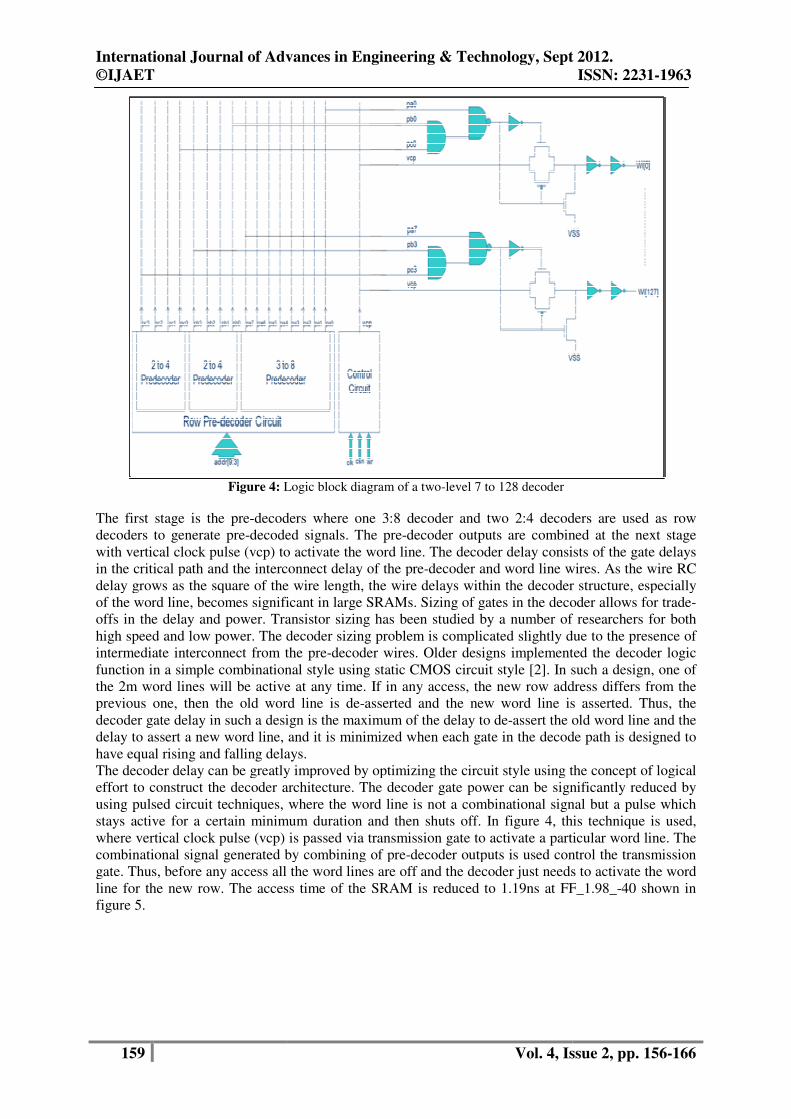
The performance (power and speed) of static CMOS decoder is based on its architecture, the number
of transistors, fan-in and the loading on the address buffer. The input buffer drive the interconnect
capacitance of address lines and also the input capacitance of the NAND gates. By using the two stage
decoder architecture the number on transistor, fan
reduced [1].As a result both speed and power are optimized. The logical diagram of a two
128 decoder is shown in Figure 4
Figure
International Journal of Advances in Engineering & Technology, Sept 2012.
Vol. 4, Issue 2, pp.
Figure 2: Self Time I/O Block
When hcp is low the dummy bit-line dmbl is charged through power supply (VDD). The dummy bit
line dmbl is connected to one input of the NAND gate G1 followed by an inverter I1. The other input
of the G1 is connected to memory enable signal which is high when the chip is selected. Hence we
will have a high echo (reset) signal. If a rising edge of the hcp occurs, the dmbl will get discharged
and we will have a low echo signal. This low echo signal resets the flip
circuit in control block and kills the corresponding word-line which is shown in fig
Concept of Power Reduction Using Multi- Stage Decoding
The performance (power and speed) of static CMOS decoder is based on its architecture, the number
in and the loading on the address buffer. The input buffer drive the interconnect
capacitance of address lines and also the input capacitance of the NAND gates. By using the two stage
decoder architecture the number on transistor, fan-in and the loading on the address input buffer is
As a result both speed and power are optimized. The logical diagram of a two
4.
Figure 3: Simulation of self-time operation
International Journal of Advances in Engineering & Technology, Sept 2012.
ISSN: 2231-1963
Vol. 4, Issue 2, pp. 156-166
power supply (VDD). The dummy bit-
line dmbl is connected to one input of the NAND gate G1 followed by an inverter I1. The other input
ignal which is high when the chip is selected. Hence we
will have a high echo (reset) signal. If a rising edge of the hcp occurs, the dmbl will get discharged
and we will have a low echo signal. This low echo signal resets the flip-flop
s shown in fig. 3.
The performance (power and speed) of static CMOS decoder is based on its architecture, the number
in and the loading on the address buffer. The input buffer drive the interconnect
capacitance of address lines and also the input capacitance of the NAND gates. By using the two stage
address input buffer is
As a result both speed and power are optimized. The logical diagram of a two-level 7 to
International Journal of Advances in Engineering & Technology, Sept 2012.
©IJAET
159
Figure 4: Logic block diagram of a two
The first stage is the pre-decoder
decoders to generate pre-decoded signals.
with vertical clock pulse (vcp) to activate the word line. The decoder delay consists of the gate delays
in the critical path and the interconnect delay of the pre
delay grows as the square of the wire length, t
of the word line, becomes significant in large SRAMs. Sizing of gates
offs in the delay and power. Transistor sizing has been studied by a number of researchers for bot
high speed and low power. The decoder sizing problem is complicated slightly due to the presence of
intermediate interconnect from the pre
function in a simple combinational style using static CM
the 2m word lines will be active at any time. If in any access, the new row address differs from the
previous one, then the old word line is de
decoder gate delay in such a design is the maximum of the delay to de
delay to assert a new word line, and it is minimized when each gate in the decode path is designed to
have equal rising and falling delays.
The decoder delay can be greatly improved by optimizing the circuit style us
effort to construct the decoder architecture
using pulsed circuit techniques, where the word line is not a combinational
stays active for a certain minimum duration and then shuts o
where vertical clock pulse (vcp) is passed via transmission gate to activate a particular word line. The
combinational signal generated by combining of pre
gate. Thus, before any access all the word lines are off and the decoder just needs to activate the word
line for the new row. The access time of the SRAM is reduced to 1.19ns at FF
figure 5.
International Journal of Advances in Engineering & Technology, Sept 2012.
Vol. 4, Issue 2, pp.
Logic block diagram of a two-level 7 to 128 decoder
decoders where one 3:8 decoder and two 2:4 decoders are used as row
decoded signals. The pre-decoder outputs are combined at the next stage
with vertical clock pulse (vcp) to activate the word line. The decoder delay consists of the gate delays
in the critical path and the interconnect delay of the pre-decoder and word line wires. As the wire RC
delay grows as the square of the wire length, the wire delays within the decoder structure, especially
of the word line, becomes significant in large SRAMs. Sizing of gates in the decoder allows for trade
offs in the delay and power. Transistor sizing has been studied by a number of researchers for bot
high speed and low power. The decoder sizing problem is complicated slightly due to the presence of
intermediate interconnect from the pre-decoder wires. Older designs implemented the decode
function in a simple combinational style using static CMOS circuit style [2]. In such a design, one of
the 2m word lines will be active at any time. If in any access, the new row address differs from the
previous one, then the old word line is de-asserted and the new word line is asserted. Thus, the
e delay in such a design is the maximum of the delay to de-assert the old word line and the
delay to assert a new word line, and it is minimized when each gate in the decode path is designed to
ual rising and falling delays.
greatly improved by optimizing the circuit style using the concept of logical
the decoder architecture. The decoder gate power can be significantly reduced by
using pulsed circuit techniques, where the word line is not a combinational signal but a pulse which
stays active for a certain minimum duration and then shuts off. In figure 4, this technique is used,
where vertical clock pulse (vcp) is passed via transmission gate to activate a particular word line. The
rated by combining of pre-decoder outputs is used control the transmission
gate. Thus, before any access all the word lines are off and the decoder just needs to activate the word
The access time of the SRAM is reduced to 1.19ns at FF
International Journal of Advances in Engineering & Technology, Sept 2012.
ISSN: 2231-1963
Vol. 4, Issue 2, pp. 156-166
one 3:8 decoder and two 2:4 decoders are used as row
s are combined at the next stage
with vertical clock pulse (vcp) to activate the word line. The decoder delay consists of the gate delays
decoder and word line wires. As the wire RC
he wire delays within the decoder structure, especially
in the decoder allows for trade-
offs in the delay and power. Transistor sizing has been studied by a number of researchers for both
high speed and low power. The decoder sizing problem is complicated slightly due to the presence of
wires. Older designs implemented the decoder logic
. In such a design, one of
the 2m word lines will be active at any time. If in any access, the new row address differs from the
asserted and the new word line is asserted. Thus, the
assert the old word line and the
delay to assert a new word line, and it is minimized when each gate in the decode path is designed to
ing the concept of logical
can be significantly reduced by
signal but a pulse which
this technique is used,
where vertical clock pulse (vcp) is passed via transmission gate to activate a particular word line. The
decoder outputs is used control the transmission
gate. Thus, before any access all the word lines are off and the decoder just needs to activate the word
The access time of the SRAM is reduced to 1.19ns at FF_1.98_-40 shown in

International Journal of Advances in Engineering & Technology, Sept 2012.
©IJAET
160
III. DESIGN GUIDELINES
When beginning a cell layout, identify critical speed paths. These paths should be prioritized when
designing the layout. Critical paths should follow
• Run signals in metal.
• Use poly only when necessary (as poly introducesa
• Do not jump signals in diffusion.
• Analog circuits, such as sense amplifiers, need to have matched layout in critical areas.
• Do not place contacts across the width of power bus metal line. Doing so reduces the
effective width on the bus. Calculate the effective metal line width by subtracting the
Width of contacts placed in the paths.
• Generally, any metal line adjacent to a wide bus should h
to avoid lithography problems. Also, signal lines running a long distance should have greater
than minimum width to reduce series resistance
• All cells should be DRC and LVS clean (except for recommended rules) before they a
called complete
• To reduce edge capacitance on the output node, divide wide gates into an even number of
legs with the output node to the inside and power to the outside. Each leg should be kept
short in order to minimize series gate resistance
• The supply connections from IO ring or supply pad to the core must be wide
• Metal width for routing should not be less than the width of the pin given in one core macro
and filler connect cell in IO ring. If metal width for connections can be increased, it is an
added advantage
Layout is a physical representation of a schematic. A set of geometric constraints or rules for a
particular manufacturing process has to be followed for the physical mask layout generation.
Geometries are determined by the electrical
the associated manufacturing process. The
International Journal of Advances in Engineering & Technology, Sept 2012.
Vol. 4, Issue 2, pp.
Figure 5: Access time simulation
UIDELINES FOR LOW POWER LAYOUT
When beginning a cell layout, identify critical speed paths. These paths should be prioritized when
designing the layout. Critical paths should follow these rules [5][15]:
necessary (as poly introducesa lot of resistance).
Do not jump signals in diffusion.
Analog circuits, such as sense amplifiers, need to have matched layout in critical areas.
contacts across the width of power bus metal line. Doing so reduces the
effective width on the bus. Calculate the effective metal line width by subtracting the
Width of contacts placed in the paths.
Generally, any metal line adjacent to a wide bus should have greater than minimum spacing
to avoid lithography problems. Also, signal lines running a long distance should have greater
than minimum width to reduce series resistance
All cells should be DRC and LVS clean (except for recommended rules) before they a
To reduce edge capacitance on the output node, divide wide gates into an even number of
legs with the output node to the inside and power to the outside. Each leg should be kept
short in order to minimize series gate resistance
y connections from IO ring or supply pad to the core must be wide
Metal width for routing should not be less than the width of the pin given in one core macro
and filler connect cell in IO ring. If metal width for connections can be increased, it is an
Layout is a physical representation of a schematic. A set of geometric constraints or rules for a
particular manufacturing process has to be followed for the physical mask layout generation.
Geometries are determined by the electrical properties of the devices and design rules pertaining to
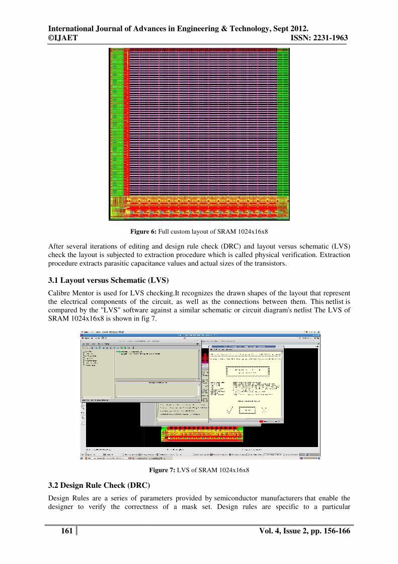
the associated manufacturing process. The full custom layout of SRAM 1024x16x8 is shown in fig
International Journal of Advances in Engineering & Technology, Sept 2012.
ISSN: 2231-1963
Vol. 4, Issue 2, pp. 156-166
When beginning a cell layout, identify critical speed paths. These paths should be prioritized when
Analog circuits, such as sense amplifiers, need to have matched layout in critical areas.
contacts across the width of power bus metal line. Doing so reduces the
effective width on the bus. Calculate the effective metal line width by subtracting the
ave greater than minimum spacing
to avoid lithography problems. Also, signal lines running a long distance should have greater
All cells should be DRC and LVS clean (except for recommended rules) before they are
To reduce edge capacitance on the output node, divide wide gates into an even number of
legs with the output node to the inside and power to the outside. Each leg should be kept
y connections from IO ring or supply pad to the core must be wide
Metal width for routing should not be less than the width of the pin given in one core macro
and filler connect cell in IO ring. If metal width for connections can be increased, it is an
Layout is a physical representation of a schematic. A set of geometric constraints or rules for a
particular manufacturing process has to be followed for the physical mask layout generation.
properties of the devices and design rules pertaining to
1024x16x8 is shown in fig 6.
International Journal of Advances in Engineering & Technology, Sept 2012.
©IJAET
161
Figure
After several iterations of editing and design rule check (DRC) and layout versus schematic (LVS)
check the layout is subjected to extraction procedure which is called physical verification. Extraction
procedure extracts parasitic capacitance values and ac
3.1 Layout versus Schematic (LVS)
Calibre Mentor is used for LVS checking
the electrical components of the circuit, as well as the connections between them. This
compared by the "LVS" software against a similar schematic or circuit diagram's
SRAM 1024x16x8 is shown in fig
3.2 Design Rule Check (DRC)
Design Rules are a series of parameters provided by
designer to verify the correctness of a mask set. Design rules are specific to a particular
International Journal of Advances in Engineering & Technology, Sept 2012.
Vol. 4, Issue 2, pp.
Figure 6: Full custom layout of SRAM 1024x16x8
After several iterations of editing and design rule check (DRC) and layout versus schematic (LVS)
check the layout is subjected to extraction procedure which is called physical verification. Extraction
procedure extracts parasitic capacitance values and actual sizes of the transistors.
Schematic (LVS)
LVS checking.It recognizes the drawn shapes of the layout that represent
the electrical components of the circuit, as well as the connections between them. This
compared by the "LVS" software against a similar schematic or circuit diagram's
own in fig 7.
Figure 7: LVS of SRAM 1024x16x8
(DRC)
Design Rules are a series of parameters provided by semiconductor manufacturers
designer to verify the correctness of a mask set. Design rules are specific to a particular
International Journal of Advances in Engineering & Technology, Sept 2012.
ISSN: 2231-1963
Vol. 4, Issue 2, pp. 156-166
After several iterations of editing and design rule check (DRC) and layout versus schematic (LVS)
check the layout is subjected to extraction procedure which is called physical verification. Extraction
tual sizes of the transistors.
recognizes the drawn shapes of the layout that represent
the electrical components of the circuit, as well as the connections between them. This netlist is
compared by the "LVS" software against a similar schematic or circuit diagram's netlist The LVS of
semiconductor manufacturers that enable the
designer to verify the correctness of a mask set. Design rules are specific to a particular
International Journal of Advances in Engineering & Technology, Sept 2012.
©IJAET
162
semiconductor manufacturing process.
checks and introduction checks are not removed.
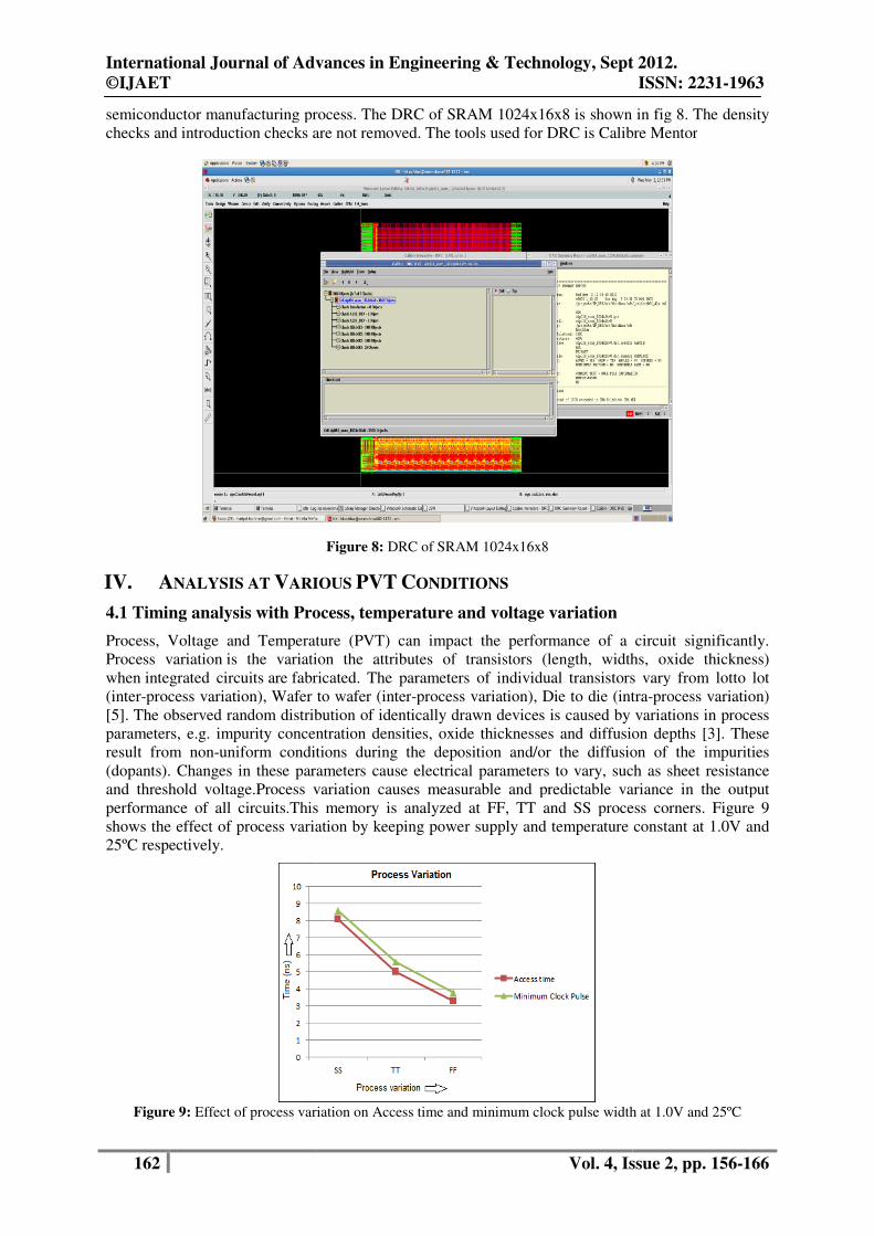
IV. ANALYSIS AT VARIOUS
4.1 Timing analysis with Process, temperature and voltage variation
Process, Voltage and Temperature (PVT) can impact the performance of a circuit significantly.
Process variation is the variation the attributes of transistors (length, widths, oxide thickness)
when integrated circuits are fabricated.
(inter-process variation), Wafer to wafer (inter
[5]. The observed random distribution of identically drawn devices is caused by variations in process
parameters, e.g. impurity concentration densities, oxide thicknesses and diffusion
result from non-uniform conditions during the deposition
(dopants). Changes in these parameters cause electrical parameters to vary, such as sheet resistance
and threshold voltage.Process variation causes measurable and predictable variance in the output
performance of all circuits.This memory is analyzed at FF, TT and SS process
shows the effect of process variation by keeping
25ºC respectively.
Figure 9: Effect of process variation on Access time and minimum clock pulse width at 1.0V and 25ºC
International Journal of Advances in Engineering & Technology, Sept 2012.
Vol. 4, Issue 2, pp.
semiconductor manufacturing process. The DRC of SRAM 1024x16x8 is shown in fig
checks and introduction checks are not removed. The tools used for DRC is Calibre Mentor
Figure 8: DRC of SRAM 1024x16x8
ARIOUS PVT CONDITIONS
Timing analysis with Process, temperature and voltage variation
Process, Voltage and Temperature (PVT) can impact the performance of a circuit significantly.
is the variation the attributes of transistors (length, widths, oxide thickness)
fabricated. The parameters of individual transistors vary from l
process variation), Wafer to wafer (inter-process variation), Die to die (intra
The observed random distribution of identically drawn devices is caused by variations in process
parameters, e.g. impurity concentration densities, oxide thicknesses and diffusion
uniform conditions during the deposition and/or the diffusion of the impurities
(dopants). Changes in these parameters cause electrical parameters to vary, such as sheet resistance
Process variation causes measurable and predictable variance in the output
This memory is analyzed at FF, TT and SS process
s variation by keeping power supply and temperature
Effect of process variation on Access time and minimum clock pulse width at 1.0V and 25ºC
International Journal of Advances in Engineering & Technology, Sept 2012.
ISSN: 2231-1963
Vol. 4, Issue 2, pp. 156-166
own in fig 8. The density
The tools used for DRC is Calibre Mentor
Process, Voltage and Temperature (PVT) can impact the performance of a circuit significantly.
is the variation the attributes of transistors (length, widths, oxide thickness)
vidual transistors vary from lotto lot
process variation), Die to die (intra-process variation)
The observed random distribution of identically drawn devices is caused by variations in process
parameters, e.g. impurity concentration densities, oxide thicknesses and diffusion depths [3]. These
and/or the diffusion of the impurities
(dopants). Changes in these parameters cause electrical parameters to vary, such as sheet resistance
Process variation causes measurable and predictable variance in the output
This memory is analyzed at FF, TT and SS process corners. Figure 9
constant at 1.0V and
Effect of process variation on Access time and minimum clock pulse width at 1.0V and 25ºC

International Journal of Advances in Engineering & Technology, Sept 2012.
©IJAET
163
Temperature is second parameter which has significant effect on the performance of a circuit.
Generally, the access time decreases
variation with process SS and Supply
Figure 10: Effect of temperature variation on Access time and minimum clock pulse width
Figure 11: Effect of supply voltage
The third parameter affecting the results is power supply voltage. Generally, the timing parameter
results are improved with increasing supply voltage but the power consumption of memory increases
with increase in supply voltage.
process and temperature constant at FF
4.2. Power analysis with Process, temperature and voltage variation
The Dynamic power analysis with respect to Proces
power is calculated at 1 MHz frequency.
International Journal of Advances in Engineering & Technology, Sept 2012.
Vol. 4, Issue 2, pp.
Temperature is second parameter which has significant effect on the performance of a circuit.
decreaseswith the increase in temperature. The effect of temperature
variation with process SS and Supply voltage 1.0 is shown in Figure 10.
Effect of temperature variation on Access time and minimum clock pulse width
supply voltage variation on Access time and minimum clock pulse width
The third parameter affecting the results is power supply voltage. Generally, the timing parameter
with increasing supply voltage but the power consumption of memory increases
with increase in supply voltage. The effect of supply voltage on timing parameters by keeping the
process and temperature constant at FF and -40C respectively is shown in Figure
. Power analysis with Process, temperature and voltage variation
The Dynamic power analysis with respect to Process variation is shown in figure
power is calculated at 1 MHz frequency. Dynamic power is least at SS and maximum at FF.
International Journal of Advances in Engineering & Technology, Sept 2012.
ISSN: 2231-1963
Vol. 4, Issue 2, pp. 156-166
Temperature is second parameter which has significant effect on the performance of a circuit.
in temperature. The effect of temperature
Effect of temperature variation on Access time and minimum clock pulse width at 1.0V_SS
variation on Access time and minimum clock pulse width at FF_ -40ºC
The third parameter affecting the results is power supply voltage. Generally, the timing parameter
with increasing supply voltage but the power consumption of memory increases
The effect of supply voltage on timing parameters by keeping the
shown in Figure 11.
s variation is shown in figure 12. The Dynamic
Dynamic power is least at SS and maximum at FF.

International Journal of Advances in Engineering & Technology, Sept 2012.
©IJAET
164
Figure 12: Dynamic Power analysis with different process corners
The Dynamic power analysis at 1MHz frequency
figure 13. As the temperature increases, the dynamic power
is analyzed for a wide temperature range from
The dynamic power is directly proportional to supply voltage i.e. it increases with increase in supply
voltage. Dynamic power analysis with respect to vol
Dynamic power is calculated at 1 MHz frequency.
Figure 13: Dynamic Power analysis with temperature variation at SS and 1.0V
Figure 14: Dynamic Power analysis with supply voltage variation at
International Journal of Advances in Engineering & Technology, Sept 2012.
Vol. 4, Issue 2, pp.
Dynamic Power analysis with different process corners at 25ºC and 1.0V
at 1MHz frequency with respect to temperature variation is shown in
. As the temperature increases, the dynamic power also increases. In this paper the memory
is analyzed for a wide temperature range from -40ºC to 85ºC. The
The dynamic power is directly proportional to supply voltage i.e. it increases with increase in supply
Dynamic power analysis with respect to voltage variation is shown in figure
Dynamic power is calculated at 1 MHz frequency.
Dynamic Power analysis with temperature variation at SS and 1.0V
Dynamic Power analysis with supply voltage variation at FF and -40ºC
International Journal of Advances in Engineering & Technology, Sept 2012.
ISSN: 2231-1963
Vol. 4, Issue 2, pp. 156-166
1.0V @ 1MHz
e variation is shown in
In this paper the memory
The dynamic power is directly proportional to supply voltage i.e. it increases with increase in supply
e variation is shown in figure 14. The
Dynamic Power analysis with temperature variation at SS and 1.0V @ 1MHz
40ºC @ 1MHz

International Journal of Advances in Engineering & Technology, Sept 2012.
©IJAET ISSN: 2231-1963
165 Vol. 4, Issue 2, pp. 156-166
V. SIMULATION RESULT
The total area of memory is 0.15mm2. The dynamic power achieved is 19.74uW at 1MHz frequency
at TT_1v_25C. The leakage current of single 6T bit-cell is 4.02pA at TT_1v_25C. The leakage power
is 53.57nW at TT_1v_25C. The access time obtained is 5ns at TT_1v_25C.
TABLE 2–Access time and cycle for various PVT conditions
Timing Definition
(ns) SS_0.9_-40 SS_1.40_85 TT_1.0_25 FF_1.98_-40
Cycle Time 16.3280 3.9063 5.4945 1.3456
Access Time 14.5338 3.5549 5.0254 1.1977
TABLE 3– Comparison with related work
Parameters This work Ref [13] Ref [14]
Size 16Kb 8Kb 1Kb
Technology 180nm 180nm 180nm
Access Time 1.1ns 1.2ns 0.5n
Dynamic power 19.7uW/MHz 41.04uW/MHz 16.4uW/MHz
Leakage power 53.57nW 26.24uW 8.2nW
Area 0.15mm2 1.0mm
2 ----
VI. CONCLUSION
A low power 16k-b SRAM has been designed using self-timed architecture, multi-stage decoding and
a full-custom layout. The work is carried out at 180nm technology. The robustness of this work is
verified by analysing this memory on a wide PVT range. The work done shoes the dependence of
power on different PVT conditions. This work has improved power as well as timing parameters by
using these techniques. A comparative analysis of this design has been done with some previous work
done showing its excellence.
TABLE 4-Feature of this SRAM
Technology 0.18um
Supply Voltage 0.9V-1.98V
Temperature -40ºC - 85ºC
Organization 16kb (1024x16cm8)
Area 0.15mm2
ACKNOWLEDGEMENTS
The authors would like to thank Mr. Syed Murtuza Hasnain, Mr. Nishant Kumar Singh who helped
during various parts of this project.
REFERENCE
[1]Martin margala, “Low- Power SRAM Circuit Design”,Department of Electrical and Computer Engineering,
University of Alberta, IEEE, 1999.
[2] David A Hodges, Horace G Jackson, Resve A Saleh “Analysis and Design of Digital Integrated Circuits”
McGraw-Hill.
[3] Tegze P.Haraszti, “CMOS memory circuits", Kluwer cademic Publishers”, 2000
[4] S. S. Rathod, Member, IEEE, S. Dasgupta, Member, IEEE and A. K. Saxena, Senior Member IEEE
“Investigation of Stack as a Low Power Design Technique for 6-T SRAM Cell” 2009 IEEE
[5] R.Jacob Baker “CMOS Circuit Design and Simulation” IEEE Series On Microelectronic Systems. WILEY
[6] S. Solanki, F. Frustaci, P. Corsonello “A Low-Leakage Single-Ended 6T SRAM Cell” Third International
Conference on Emerging Trends in Engineering and Technology,2010 IEEE

International Journal of Advances in Engineering & Technology, Sept 2012.
©IJAET ISSN: 2231-1963
166 Vol. 4, Issue 2, pp. 156-166
[7] Keejong Kim, Hamid Mahmoodi, Kaushik Roy” A Low-Power SRAM Using Bit-Line Charge-Recycling”
IEEE Journal Of Solid-State Circuit ,February 2008
[8] K.Dhanumjaya, Dr.MN.Giri Prasad, Dr.K.Padmaraju,Dr.M.Raja Reddy, “ Design of Low Power SRAM in
45 nm CMOS Technology” international Journal of Engineering Research and Applications (IJERA) ISSN:
2248-9622
[9] Byung-Do Yang, “A Low-Power SRAM Using Bit-Line Charge-Recycling for Read and Write Operations”
IEEE Journal Of Solid-State Circuits, 2010
[10] K. W. Mai et al., “Low-power SRAM design using half-swing pulse-mode techniques,” IEEE J. Solid-State
Circuits, vol. 33, no. 11, pp. 1659–1671, Nov. 1998.
[11] K. Kanda, H. Sadaaki, and T. Sakurai, “90% write power-saving SRAM using sense-amplifying memory
cell,” IEEE J. Solid-State Circuits, vol. 39, no. 6, pp. 927–933, Jun. 2004.
[12] B.-D. Yang and L.-S. Kim, “A low-power SRAM using hierachical bit line and local sense amplifiers,”
IEEE J. Solid-State Circuits, vol. 40, no. 6, pp. 1366–1376, Jun. 2005.
[13] Sreerama Reddy G M and P Chandrasekhara Reddy, “Design and Implementation of 8K-bits Low Power
SRAM in 180nm Technology,” IMECS, vol. II, March. 2009.
[14]Tadayoshi Enomoto and Yuki Higuchi, “A Low-leakage Current Power 180-nm CMOS SRAM,” IEEE,
2008
[15] Sreerama Reddy G M and P Chandrasekhara Reddy, “Design and VLSI Implementation of 8 Mb Low
Power SRAM in 90nm,” EJSR, vol.26 No.2,pp.305-314. 2009.
AUTHORS Haripal Kochhar, a M.Tech scholar at the Panjab University Chandigarh, India. He is
working as Design Engineer at RF Silicon Tech. Pvt. Ltd., Delhi, India. He has received his
B.Tech. in Electronics and Communication Engineering from Punjab Technical University,
Jalandhar (Pb.) in the year of 2010. His main research interest is in low power memory
design.
Subodh Kansalis working as Design Engineer at RF Silicon Tech. Pvt. Ltd., Delhi, India. He
has received his B.Tech. in Electronics and Communication Engineering from Institute of
Engineering & Technology, Bhaddal,Ropar (Pb.) affiliated to Punjab Technical University,
Jalandhar (Pb.) in the year of 2011. His main research interest is in low power and high
speed memory design.
Sharmelee Thangjam, a P.hd scholar from Panjab University, Chandigarh, India.Sheis
working as Assistant Professor, Panjab University Chandigarh, India. She has received her
M.E. from Thapar University, Patiala, Punjab and B.E. from University of Madras in year
2002 and 2000 respectively. Her main research interest is in Signal Processing, VLSI design.