Embed Size (px)
Citation preview
17.5 GHz to 24 GHz, GaAs, MMIC, I/Q Downconverter
Data Sheet ADMV1012
Rev. A Document Feedback Information furnished by Analog Devices is believed to be accurate and reliable. However, no responsibility is assumed by Analog Devices for its use, nor for any infringements of patents or other rights of third parties that may result from its use. Specifications subject to change without notice. No license is granted by implication or otherwise under any patent or patent rights of Analog Devices. Trademarks and registered trademarks are the property of their respective owners.
One Technology Way, P.O. Box 9106, Norwood, MA 02062-9106, U.S.A. Tel: 781.329.4700 ©2017–2018 Analog Devices, Inc. All rights reserved. Technical Support www.analog.com
FEATURES RF input frequency range: 17.5 GHz to 24 GHz IF output frequency range: 2.5 GHz to 3.5 GHz LO input frequency range: 7 GHz to 13.5 GHz Conversion gain (with hybrid): 15 dB typical SSB noise figure: 2.5 dB typical Input IP3: 3 dBm typical Input P1dB: −5 dBm typical 25 dB of image rejection Single-ended, 50 Ω RF and LO input ports Exposed pad, 4.9 mm × 4.9 mm, 32-terminal LCC
APPLICATIONS Point to point microwave radios Radars and electronic warfare systems Instrumentation, automatic test equipment (ATE) Satellite communications
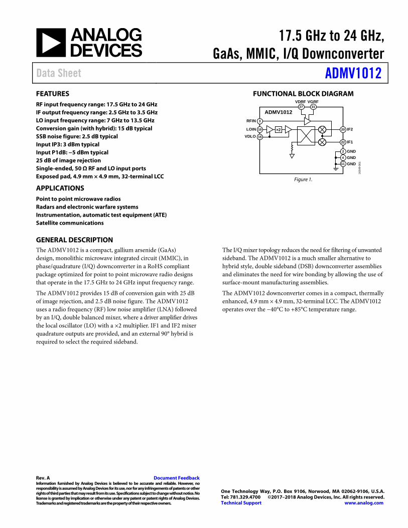
FUNCTIONAL BLOCK DIAGRAM
31
2010
3
1522
27
×2 IF2LOIN
RFIN
VDRF VGRF
VDLOIF1
ADMV1012
1634
9-00
1
2
4
GNDGND
11 GND
Figure 1.
GENERAL DESCRIPTION The ADMV1012 is a compact, gallium arsenide (GaAs) design, monolithic microwave integrated circuit (MMIC), in phase/quadrature (I/Q) downconverter in a RoHS compliant package optimized for point to point microwave radio designs that operate in the 17.5 GHz to 24 GHz input frequency range.
The ADMV1012 provides 15 dB of conversion gain with 25 dB of image rejection, and 2.5 dB noise figure. The ADMV1012 uses a radio frequency (RF) low noise amplifier (LNA) followed by an I/Q, double balanced mixer, where a driver amplifier drives the local oscillator (LO) with a ×2 multiplier. IF1 and IF2 mixer quadrature outputs are provided, and an external 90° hybrid is required to select the required sideband.
The I/Q mixer topology reduces the need for filtering of unwanted sideband. The ADMV1012 is a much smaller alternative to hybrid style, double sideband (DSB) downconverter assemblies and eliminates the need for wire bonding by allowing the use of surface-mount manufacturing assemblies.
The ADMV1012 downconverter comes in a compact, thermally enhanced, 4.9 mm × 4.9 mm, 32-terminal LCC. The ADMV1012 operates over the −40°C to +85°C temperature range.
ADMV1012 Data Sheet
Rev. A | Page 2 of 19
TABLE OF CONTENTS Features .............................................................................................. 1
Applications ....................................................................................... 1
Functional Block Diagram .............................................................. 1
General Description ......................................................................... 1
Revision History ............................................................................... 2
Specifications ..................................................................................... 3
Absolute Maximum Ratings ............................................................ 4
Thermal Resistance ...................................................................... 4
ESD Caution .................................................................................. 4
Pin Configuration and Function Descriptions ............................. 5
Typical Performance Characteristics ............................................. 6
Upper Sideband (Low-Side LO) ................................................. 6
Lower Sideband (High-Side LO) ................................................ 8
IF Bandwidth .............................................................................. 10
Leakage Performance ................................................................. 11
Return Loss Performance .......................................................... 12
Spurious Performance ............................................................... 13
M × N Spurious Performance for LO = 0 dBm ...................... 13
Theory of Operation ...................................................................... 14
LO Driver Amplifier .................................................................. 14
Mixer ............................................................................................ 14
LNA .............................................................................................. 14
Applications Information .............................................................. 15
Typical Application Circuit ....................................................... 15
Evaluation Board Information ................................................. 16
Bill of Materials ........................................................................... 18
Outline Dimensions ....................................................................... 19
Ordering Guide .......................................................................... 19
REVISION HISTORY 2/2018—Rev. 0 to Rev. A Changes to Features Section, General Description Section, and Figure 1 .............................................................................................. 1 Changes to Table 1 ............................................................................ 3 Changes to Table 2 ............................................................................ 4 Added Thermal Resistance Section and Table 3; Renumbered Sequentially ....................................................................................... 4 Changes to Figure 2 and Table 4 ..................................................... 5 Changes to Figure 3 and Figure 6 ................................................... 6 Changes to Figure 12 ........................................................................ 7 Changes to Figure 24, Figure 25, and Figure 26 ......................... 10 Changes to Figure 27 through Figure 30 ..................................... 11
Changed M × N Spurious Performance for LO = 4 dBm Section to M × N Spurious Performance for LO = 0 dBm Section ....... 13 Changes to M × N Spurious Performance for LO = 0 dBm Section .............................................................................................. 13 Changes to LO Driver Amplifier Section .................................... 14 Changes to Applications Information Section and Figure 34 ........ 15 Changes to Power-On Sequence Section .................................... 16 Changes to Figure 37 ...................................................................... 17 Changes to Table 6 .......................................................................... 18 Changes to Ordering Guide .......................................................... 19
10/2017—Revision 0: Initial Version
Data Sheet ADMV1012
Rev. A | Page 3 of 19
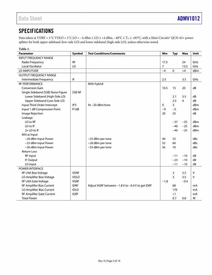
SPECIFICATIONS Data taken at VDRF = 3 V, VDLO = 3 V, LO = −4 dBm ≤ LO ≤ +4 dBm, −40°C ≤ TA ≤ +85°C, with a Mini-Circuits® QCN-45+ power splitter for both upper sideband (low-side LO) and lower sideband (high-side LO), unless otherwise noted.
Table 1. Parameter Symbol Test Conditions/Comments Min Typ Max Unit INPUT FREQUENCY RANGE
Radio Frequency RF 17.5 24 GHz Local Oscillator LO 7 13.5 GHz
LO AMPLITUDE −4 0 +4 dBm OUTPUT FREQUENCY RANGE
Intermediate Frequency IF 2.5 3.5 GHz RF PERFORMANCE With hybrid
Conversion Gain 10.5 15 20 dB Single Sideband (SSB) Noise Figure SSB NF
Lower Sideband (High-Side LO) 2.1 3.5 dB Upper Sideband (Low-Side LO) 2.5 4 dB
Input Third-Order Intercept IP3 At −20 dBm/tone 0 3 dBm Input 1 dB Compression Point P1dB −9 −5 dBm Image Rejection 20 25 dB Leakage
LO to RF −37 −25 dBm LO to IF −40 −25 dBm 2× LO to IF −40 −25 dBm
IM3 at Input −20 dBm Input Power −23 dBm per tone 46 52 dBc −25 dBm Input Power −28 dBm per tone 52 60 dBc −30 dBm Input Power −33 dBm per tone 56 70 dBc
Return Loss RF Input −11 −10 dB IF Output −23 −10 dB LO Input −11 −10 dB
POWER INTERFACE RF LNA Bias Voltage VDRF 3 3.5 V LO Amplifier Bias Voltage VDLO 3 3.5 V RF LNA Gate Voltage VGRF −1.8 −0.4 RF Amplifier Bias Current IDRF Adjust VGRF between −1.8 V to −0.4 V to get IDRF 68 mA LO Amplifier Bias Current IDLO 170 mA RF Amplifier Gate Current IGRF <1 mA Total Power 0.7 0.8 W

ADMV1012 Data Sheet
Rev. A | Page 4 of 19
ABSOLUTE MAXIMUM RATINGS Table 2. Parameter Rating Supply Voltage
VDLO 4 V VGRF 0 V VDRF − VGRF1 6 V
Input Power RF 15 dBm LO 15 dBm
Maximum Junction Temperature 175°C Maximum Power Dissipation 2 W Lifetime at Maximum Junction Temperature (TJ) >1 million hours Operating Temperature Range −40°C to +85°C Storage Temperature Range −65°C to +150°C Lead Temperature (Soldering 60 sec) 260°C Moisture Sensitivity Level (MSL) Rating MSL3 Electrostatic Discharge (ESD) Sensitivity
Human Body Model (HBM) 750 V Field Induced Charged Device Model
(FICDM) 500 V
1 The maximum VDRF voltage and the minimum VGRF voltage is determined by this difference. If a maximum VDRF voltage of +4 V is required, then the minimum VGRF voltage is −2 V.
Stresses at or above those listed under Absolute Maximum Ratings may cause permanent damage to the product. This is a stress rating only; functional operation of the product at these or any other conditions above those indicated in the operational section of this specification is not implied. Operation beyond the maximum operating conditions for extended periods may affect product reliability.
THERMAL RESISTANCE Thermal performance is directly linked to printed circuit board (PCB) design and operating environment. Careful attention to PCB thermal design is required.
θJA is thermal resistance, junction to ambient (°C/W), and θJC is thermal resistance, junction to case (°C/W).
Table 3. Thermal Resistance Package Type θJA
1 θJC Unit E-32-1 33.4 34 °C/W 1 See JEDEC standard JESD51-2 for additional information on optimizing the
thermal impedance (PCB with 3 × 3 vias).
ESD CAUTION
Data Sheet ADMV1012
Rev. A | Page 5 of 19
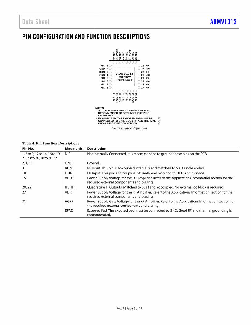
PIN CONFIGURATION AND FUNCTION DESCRIPTIONS
24 NIC23 NIC22 IF121 NIC20 IF219 NIC18 NIC17 NIC
12345678
NICGNDRFINGNDNICNICNICNIC
9 10 11 12 13 14 15 16
NIC
LOIN
GN
DN
ICN
ICN
ICVD
LO NIC
32 31 30 29 28 27 26 25
NIC
VGR
FN
ICN
ICN
ICVD
RF
NIC
NIC
ADMV1012TOP VIEW
(Not to Scale)
1634
9-00
2
NOTES1. NIC = NOT INTERNALLY CONNECTED. IT IS RECOMMENDED TO GROUND THESE PINS ON THE PCB.2. EXPOSED PAD. THE EXPOSED PAD MUST BE CONNECTED TO GND. GOOD RF AND THERMAL GROUNDING IS RECOMMENDED.
Figure 2. Pin Configuration
Table 4. Pin Function Descriptions Pin No. Mnemonic Description 1, 5 to 9, 12 to 14, 16 to 19, 21, 23 to 26, 28 to 30, 32
NIC Not Internally Connected. It is recommended to ground these pins on the PCB.
2, 4, 11 GND Ground. 3 RFIN RF Input. This pin is ac-coupled internally and matched to 50 Ω single ended. 10 LOIN LO Input. This pin is ac-coupled internally and matched to 50 Ω single ended. 15 VDLO Power Supply Voltage for the LO Amplifier. Refer to the Applications Information section for the
required external components and biasing. 20, 22 IF2, IF1 Quadrature IF Outputs. Matched to 50 Ω and ac coupled. No external dc block is required. 27 VDRF Power Supply Voltage for the RF Amplifier. Refer to the Applications Information section for the
required external components and biasing. 31 VGRF Power Supply Gate Voltage for the RF Amplifier. Refer to the Applications Information section for
the required external components and biasing. EPAD Exposed Pad. The exposed pad must be connected to GND. Good RF and thermal grounding is
recommended.
ADMV1012 Data Sheet
Rev. A | Page 6 of 19
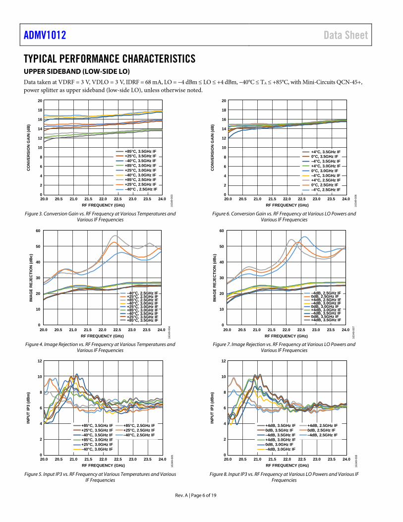
TYPICAL PERFORMANCE CHARACTERISTICS UPPER SIDEBAND (LOW-SIDE LO) Data taken at VDRF = 3 V, VDLO = 3 V, IDRF = 68 mA, LO = −4 dBm ≤ LO ≤ +4 dBm, −40°C ≤ TA ≤ +85°C, with Mini-Circuits QCN-45+, power splitter as upper sideband (low-side LO), unless otherwise noted.
20
0
2
4
6
8
10
12
14
16
18
20.0 20.5 21.0 21.5 22.0 22.5 23.0 23.5 24.0
CO
NVE
RSI
ON
GA
IN (d
B)
RF FREQUENCY (GHz)
+85°C, 3.5GHz IF+25°C, 3.5GHz IF–40°C, 3.5GHz IF+85°C, 3.0GHz IF+25°C, 3.0GHz IF–40°C, 3.0GHz IF+85°C, 2.5GHz IF+25°C, 2.5GHz IF–40°C , 2.5GHz IF
1634
9-00
3
Figure 3. Conversion Gain vs. RF Frequency at Various Temperatures and
Various IF Frequencies
0
10
20
30
40
50
60
20.0 20.5 21.0 21.5 22.0 22.5 23.0 23.5 24.0
IMA
GE
REJ
ECTI
ON
(dB
c)
RF FREQUENCY (GHz)
–40°C, 2.5GHz IF+25°C, 2.5GHz IF+85°C, 2.5GHz IF–40°C, 3.0GHz IF+25°C, 3.0GHz IF+85°C, 3.0GHz IF–40°C, 3.5GHz IF+25°C, 3.5GHz IF+85°C, 3.5GHz IF
1634
9-00
4
Figure 4. Image Rejection vs. RF Frequency at Various Temperatures and
Various IF Frequencies
12
0
2
4
6
8
10
20.0 20.5 21.0 21.5 22.0 22.5 23.0 23.5 24.0
INPU
T IP
3 (d
Bm
)
RF FREQUENCY (GHz)
+85°C, 3.5GHz IF+25°C, 3.5GHz IF–40°C, 3.5GHz IF+85°C, 3.0GHz IF+25°C, 3.0GHz IF–40°C, 3.0GHz IF
+85°C, 2.5GHz IF+25°C, 2.5GHz IF–40°C, 2.5GHz IF
1634
9-00
5
Figure 5. Input IP3 vs. RF Frequency at Various Temperatures and Various
IF Frequencies
20
18
0
2
4
6
8
10
12
14
16
20.0 20.5 21.0 21.5 22.0 22.5 23.0 23.5 24.0
CO
NVE
RSI
ON
GA
IN (d
B)
RF FREQUENCY (GHz)
+4°C, 3.5GHz IF0°C, 3.5GHz IF–4°C, 3.5GHz IF+4°C, 3.0GHz IF0°C, 3.0GHz IF–4°C, 3.0GHz IF+4°C, 2.5GHz IF0°C, 2.5GHz IF–4°C, 2.5GHz IF
1634
9-00
6
Figure 6. Conversion Gain vs. RF Frequency at Various LO Powers and
Various IF Frequencies
0
10
20
30
40
50
60
20.0 20.5 21.0 21.5 22.0 22.5 23.0 23.5 24.0
IMA
GE
REJ
ECTI
ON
( dB
c)
RF FREQUENCY (GHz) 1634
9-00
7
–4dB, 2.5GHz IF0dB, 2.5GHz IF+4dB, 2.5GHz IF–4dB, 3.0GHz IF0dB, 3.0GHz IF+4dB, 3.0GHz IF–4dB, 3.5GHz IF0dB, 3.5GHz IF+4dB, 3.5GHz IF
Figure 7. Image Rejection vs. RF Frequency at Various LO Powers and
Various IF Frequencies
12
0
2
4
6
8
10
20.0 20.5 21.0 21.5 22.0 22.5 23.0 23.5 24.0
INPU
T IP
3 (d
Bm
)
RF FREQUENCY (GHz)
+4dB, 3.5GHz IF0dB, 3.5GHz IF–4dB, 3.5GHz IF+4dB, 3.0GHz IF0dB, 3.0GHz IF–4dB, 3.0GHz IF
+4dB, 2.5GHz IF0dB, 2.5GHz IF–4dB, 2.5GHz IF
1634
9-00
8
Figure 8. Input IP3 vs. RF Frequency at Various LO Powers and Various IF
Frequencies
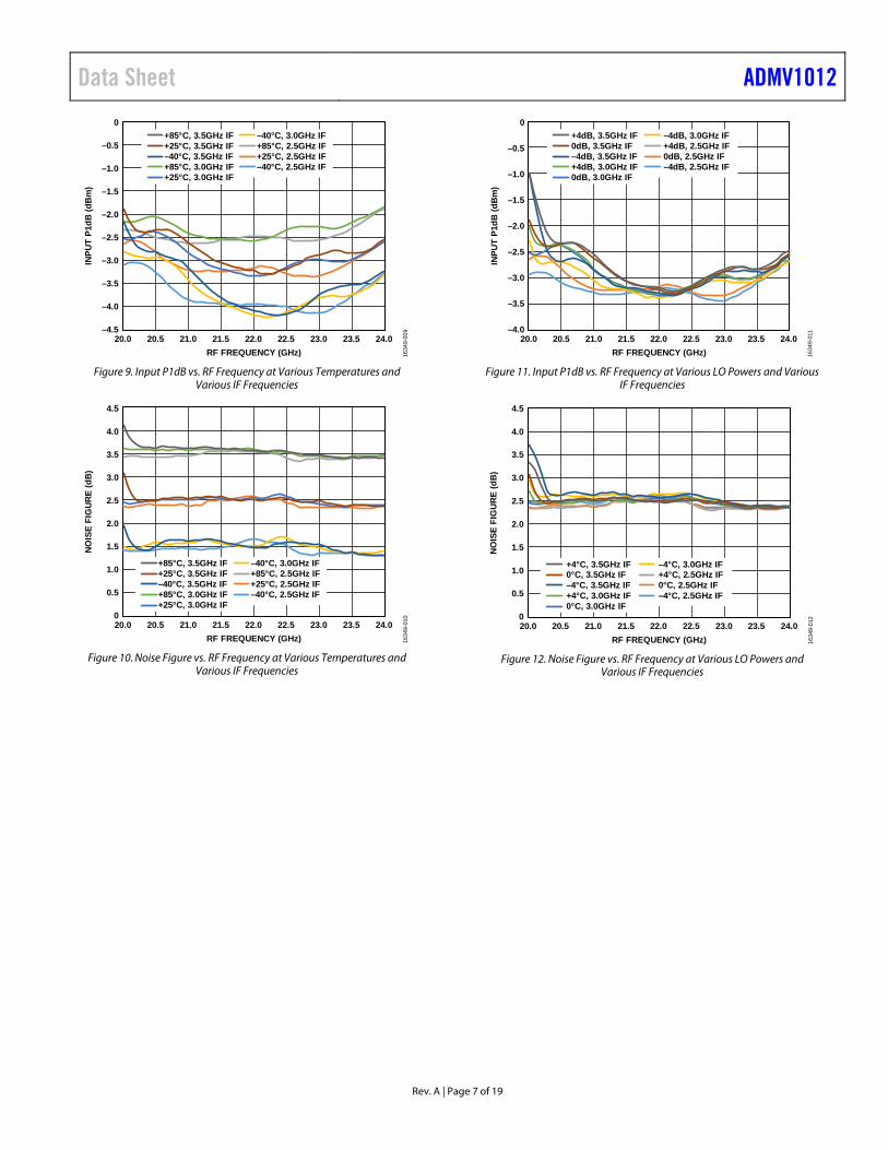
Data Sheet ADMV1012
Rev. A | Page 7 of 19
0
–4.5
–1.0
–0.5
–2.0
–1.5
–3.0
–2.5
–4.0
–3.5
20.0 20.5 21.0 21.5 22.0 22.5 23.0 23.5 24.0
INPU
T P1
dB (d
Bm
)
RF FREQUENCY (GHz)
+85°C, 3.5GHz IF+25°C, 3.5GHz IF–40°C, 3.5GHz IF+85°C, 3.0GHz IF+25°C, 3.0GHz IF
–40°C, 3.0GHz IF+85°C, 2.5GHz IF+25°C, 2.5GHz IF–40°C, 2.5GHz IF
1634
9-00
9
Figure 9. Input P1dB vs. RF Frequency at Various Temperatures and
Various IF Frequencies
4.5
0
0.5
1.0
1.5
2.0
2.5
3.0
3.5
4.0
20.0 20.5 21.0 21.5 22.0 22.5 23.0 23.5 24.0
NO
ISE
FIG
UR
E (d
B)
RF FREQUENCY (GHz)
+85°C, 3.5GHz IF+25°C, 3.5GHz IF–40°C, 3.5GHz IF+85°C, 3.0GHz IF+25°C, 3.0GHz IF
–40°C, 3.0GHz IF+85°C, 2.5GHz IF+25°C, 2.5GHz IF–40°C, 2.5GHz IF
1634
9-01
0
Figure 10. Noise Figure vs. RF Frequency at Various Temperatures and
Various IF Frequencies
0
–4.0
–1.0
–0.5
–2.0
–1.5
–3.0
–2.5
–3.5
20.0 20.5 21.0 21.5 22.0 22.5 23.0 23.5 24.0
INPU
T P1
dB (d
Bm
)
RF FREQUENCY (GHz)
+4dB, 3.5GHz IF0dB, 3.5GHz IF–4dB, 3.5GHz IF+4dB, 3.0GHz IF0dB, 3.0GHz IF
–4dB, 3.0GHz IF+4dB, 2.5GHz IF0dB, 2.5GHz IF–4dB, 2.5GHz IF
1634
9-01
1
Figure 11. Input P1dB vs. RF Frequency at Various LO Powers and Various
IF Frequencies
4.5
4.0
0
0.5
1.0
1.5
2.0
2.5
3.0
3.5
20.0 20.5 21.0 21.5 22.0 22.5 23.0 23.5 24.0
NO
ISE
FIG
UR
E (d
B)
RF FREQUENCY (GHz)
+4°C, 3.5GHz IF0°C, 3.5GHz IF–4°C, 3.5GHz IF+4°C, 3.0GHz IF0°C, 3.0GHz IF
–4°C, 3.0GHz IF+4°C, 2.5GHz IF0°C, 2.5GHz IF–4°C, 2.5GHz IF
1634
9-01
2
Figure 12. Noise Figure vs. RF Frequency at Various LO Powers and
Various IF Frequencies
ADMV1012 Data Sheet
Rev. A | Page 8 of 19
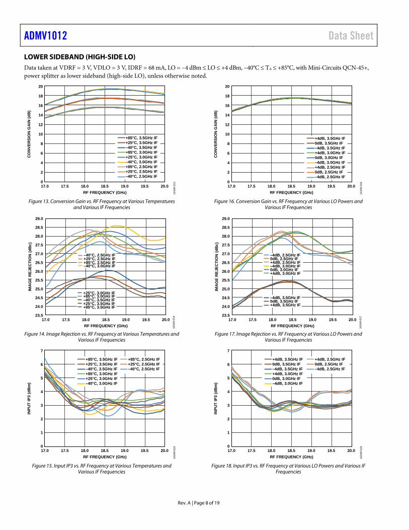
LOWER SIDEBAND (HIGH-SIDE LO) Data taken at VDRF = 3 V, VDLO = 3 V, IDRF = 68 mA, LO = −4 dBm ≤ LO ≤ +4 dBm, −40°C ≤ TA ≤ +85°C, with Mini-Circuits QCN-45+, power splitter as lower sideband (high-side LO), unless otherwise noted.
20
0
2
4
6
8
10
12
14
16
18
17.0 17.5 18.0 18.5 19.0 19.5 20.0
CO
NVE
RSI
ON
GA
IN (d
B)
RF FREQUENCY (GHz)
+85°C, 3.5GHz IF+25°C, 3.5GHz IF–40°C, 3.5GHz IF+85°C, 3.0GHz IF+25°C, 3.0GHz IF–40°C, 3.0GHz IF+85°C, 2.5GHz IF+25°C, 2.5GHz IF–40°C, 2.5GHz IF
1634
9-01
3
Figure 13. Conversion Gain vs. RF Frequency at Various Temperatures
and Various IF Frequencies
23.5
24.0
24.5
25.0
25.5
26.0
26.5
27.0
27.5
28.0
28.5
29.0
17.0 17.5 18.0 18.5 19.0 19.5 20.0
IMA
GE
REJ
ECTI
ON
(dB
c)
RF FREQUENCY (GHz)
–40°C, 2.5GHz IF+25°C, 2.5GHz IF+85°C, 2.5GHz IF–40°C, 3.0GHz IF
+25°C, 3.0GHz IF+85°C, 3.0GHz IF–40°C, 3.5GHz IF+25°C, 3.5GHz IF+85°C, 3.5GHz IF
1634
9-01
4
Figure 14. Image Rejection vs. RF Frequency at Various Temperatures and
Various IF Frequencies
7
0
1
2
3
4
5
6
17.0 17.5 18.0 18.5 19.0 19.5 20.0
INPU
T IP
3 (d
Bm
)
RF FREQUENCY (GHz)
+85°C, 3.5GHz IF+25°C, 3.5GHz IF–40°C, 3.5GHz IF+85°C, 3.0GHz IF+25°C, 3.0GHz IF–40°C, 3.0GHz IF
+85°C, 2.5GHz IF+25°C, 2.5GHz IF–40°C, 2.5GHz IF
1634
9-01
5
Figure 15. Input IP3 vs. RF Frequency at Various Temperatures and
Various IF Frequencies
20
0
2
4
6
8
10
12
14
16
18
17.0 17.5 18.0 18.5 19.0 19.5 20.0
CO
NVE
RSI
ON
GA
IN (d
B)
RF FREQUENCY (GHz)
+4dB, 3.5GHz IF0dB, 3.5GHz IF–4dB, 3.5GHz IF+4dB, 3.0GHz IF0dB, 3.0GHz IF–4dB, 3.0GHz IF+4dB, 2.5GHz IF0dB, 2.5GHz IF–4dB, 2.5GHz IF
1634
9-01
6
Figure 16. Conversion Gain vs. RF Frequency at Various LO Powers and
Various IF Frequencies
23.5
24.0
24.5
25.0
25.5
26.0
26.5
27.0
27.5
28.0
28.5
29.0
17.0 17.5 18.0 18.5 19.0 19.5 20.0
IMA
GE
REJ
ECTI
ON
(dB
c)
RF FREQUENCY (GHz) 1634
9-01
7
–4dB, 2.5GHz IF0dB, 2.5GHz IF+4dB, 2.5GHz IF–4dB, 3.0GHz IF0dB, 3.0GHz IF+4dB, 3.0GHz IF
–4dB, 3.5GHz IF0dB, 3.5GHz IF+4dB, 3.5GHz IF
Figure 17. Image Rejection vs. RF Frequency at Various LO Powers and
Various IF Frequencies
7
0
1
2
3
4
5
6
17.0 17.5 18.0 18.5 19.0 19.5 20.0
INPU
T IP
3 (d
Bm
)
RF FREQUENCY (GHz)
+4dB, 3.5GHz IF0dB, 3.5GHz IF–4dB, 3.5GHz IF+4dB, 3.0GHz IF0dB, 3.0GHz IF–4dB, 3.0GHz IF
+4dB, 2.5GHz IF0dB, 2.5GHz IF–4dB, 2.5GHz IF
1634
9-01
8
Figure 18. Input IP3 vs. RF Frequency at Various LO Powers and Various IF
Frequencies
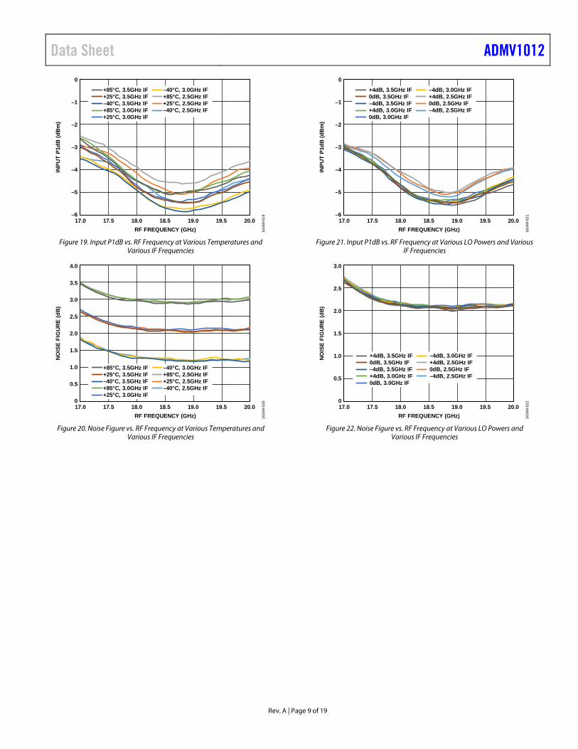
Data Sheet ADMV1012
Rev. A | Page 9 of 19
0
–6
–5
–4
–3
–2
–1
17.0 17.5 18.0 18.5 19.0 19.5 20.0
INPU
T P1
dB (d
Bm
)
RF FREQUENCY (GHz)
+85°C, 3.5GHz IF+25°C, 3.5GHz IF–40°C, 3.5GHz IF+85°C, 3.0GHz IF+25°C, 3.0GHz IF
–40°C, 3.0GHz IF+85°C, 2.5GHz IF+25°C, 2.5GHz IF–40°C, 2.5GHz IF
1634
9-01
9
Figure 19. Input P1dB vs. RF Frequency at Various Temperatures and
Various IF Frequencies
4.0
0
0.5
1.0
1.5
2.0
2.5
3.0
3.5
17.0 17.5 18.0 18.5 19.0 19.5 20.0
NO
ISE
FIG
UR
E (d
B)
RF FREQUENCY (GHz)
+85°C, 3.5GHz IF+25°C, 3.5GHz IF–40°C, 3.5GHz IF+85°C, 3.0GHz IF+25°C, 3.0GHz IF
–40°C, 3.0GHz IF+85°C, 2.5GHz IF+25°C, 2.5GHz IF–40°C, 2.5GHz IF
1634
9-02
0
Figure 20. Noise Figure vs. RF Frequency at Various Temperatures and
Various IF Frequencies
0
–6
–5
–4
–3
–2
–1
17.0 17.5 18.0 18.5 19.0 19.5 20.0
INPU
T P1
dB (d
Bm
)
RF FREQUENCY (GHz)
+4dB, 3.5GHz IF0dB, 3.5GHz IF–4dB, 3.5GHz IF+4dB, 3.0GHz IF0dB, 3.0GHz IF
–4dB, 3.0GHz IF+4dB, 2.5GHz IF0dB, 2.5GHz IF–4dB, 2.5GHz IF
1634
9-02
1
Figure 21. Input P1dB vs. RF Frequency at Various LO Powers and Various
IF Frequencies
3.0
0
0.5
1.0
1.5
2.0
2.5
17.0 17.5 18.0 18.5 19.0 19.5 20.0
NO
ISE
FIG
UR
E (d
B)
RF FREQUENCY (GHz)
+4dB, 3.5GHz IF0dB, 3.5GHz IF–4dB, 3.5GHz IF+4dB, 3.0GHz IF0dB, 3.0GHz IF
–4dB, 3.0GHz IF+4dB, 2.5GHz IF0dB, 2.5GHz IF–4dB, 2.5GHz IF
1634
9-02
2
Figure 22. Noise Figure vs. RF Frequency at Various LO Powers and
Various IF Frequencies

ADMV1012 Data Sheet
Rev. A | Page 10 of 19
IF BANDWIDTH Data taken at VDRF = 3 V, VDLO = 3 V, IDRF = 68 mA, LO = −4 dBm ≤ LO ≤ +4 dBm at 10 GHz, −40°C ≤ TA ≤ +85°C, with Mini-Circuits QCN-45+, power splitter, unless otherwise noted.
25
0
5
15
10
20
2.0 2.2 2.4 2.6 2.8 3.0 3.2 3.63.4 3.8 4.0
CO
NVE
RSI
ON
GA
IN (d
B)
IF FREQUENCY (GHz)
+85°C, UPPER+25°C, UPPER–40°C, UPPER+85°C, LOWER+25°C, LOWER–40°C, LOWER
1634
9-02
3
Figure 23. Conversion Gain vs. IF Frequency at Various Temperatures and
Sidebands
10
0
2
6
4
8
9
1
5
3
7
2.0 2.2 2.4 2.6 2.8 3.0 3.2 3.63.4 3.8 4.0
INPU
T IP
3 (d
Bm
)
IF FREQUENCY (GHz)
+85°C, UPPER+25°C, UPPER–40°C, UPPER+85°C, LOWER+25°C, LOWER–40°C, LOWER
1634
9-02
5
Figure 24. Input IP3 vs. IF Frequency at Various Temperatures and
Sidebands
25
20
0
15
10
5
2.0 2.2 2.4 2.6 2.8 3.0 3.2 3.63.4 3.8 4.0
CO
NVE
RSI
ON
GA
IN (d
B)
IF FREQUENCY (GHz)
+4dBm, UPPER0dBm, UPPER–4dBm, UPPER+4dBm, LOWER0dBm, LOWER–4dBm, LOWER
1634
9-02
6
Figure 25. Conversion Gain vs. IF Frequency at Various LO Powers and
Sidebands
10
9
0
2
6
4
8
1
5
3
7
2.0 2.2 2.4 2.6 2.8 3.0 3.2 3.63.4 3.8 4.0
INPU
T IP
3 (d
Bm
)
IF FREQUENCY (GHz)
+4dBm, UPPER0dBm, UPPER–4dBm, UPPER+4dBm, LOWER0dBm, LOWER–4dBm, LOWER
1634
9-02
8
Figure 26. Input IP3 vs. IF Frequency at Various LO Powers and Sidebands
Data Sheet ADMV1012
Rev. A | Page 11 of 19
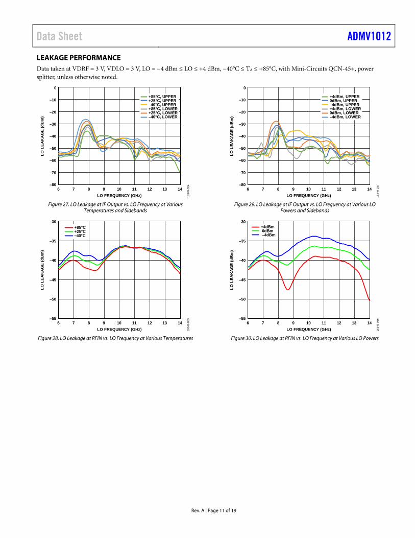
LEAKAGE PERFORMANCE Data taken at VDRF = 3 V, VDLO = 3 V, LO = −4 dBm ≤ LO ≤ +4 dBm, −40°C ≤ TA ≤ +85°C, with Mini-Circuits QCN-45+, power splitter, unless otherwise noted.
0
–80
–60
–40
–20
–70
–50
–30
–10
6 7 8 9 10 11 12 13 14
LO L
EAK
AG
E (d
Bm
)
LO FREQUENCY (GHz)
+85°C, UPPER+25°C, UPPER–40°C, UPPER+85°C, LOWER+25°C, LOWER–40°C, LOWER
1634
9-03
4
Figure 27. LO Leakage at IF Output vs. LO Frequency at Various
Temperatures and Sidebands
–30
–55
–50
–45
–40
–35
6 7 8 9 10 11 12 13 14
LO L
EAK
AG
E (d
Bm
)
LO FREQUENCY (GHz)
+85°C+25°C–40°C
1634
9-03
3
Figure 28. LO Leakage at RFIN vs. LO Frequency at Various Temperatures
0
–80
–60
–40
–20
–70
–50
–30
–10
6 7 8 9 10 11 12 13 14
LO L
EAK
AG
E (d
Bm
)
LO FREQUENCY (GHz)
+4dBm, UPPER0dBm, UPPER–4dBm, UPPER+4dBm, LOWER0dBm, LOWER–4dBm, LOWER
1634
9-03
7
Figure 29. LO Leakage at IF Output vs. LO Frequency at Various LO
Powers and Sidebands
–30
–55
–50
–45
–40
–35
6 7 8 9 10 11 12 13 14
LO L
EAK
AG
E (d
Bm
)
LO FREQUENCY (GHz)
+4dBm 0dBm –4dBm
1634
9-03
6
Figure 30. LO Leakage at RFIN vs. LO Frequency at Various LO Powers
ADMV1012 Data Sheet
Rev. A | Page 12 of 19
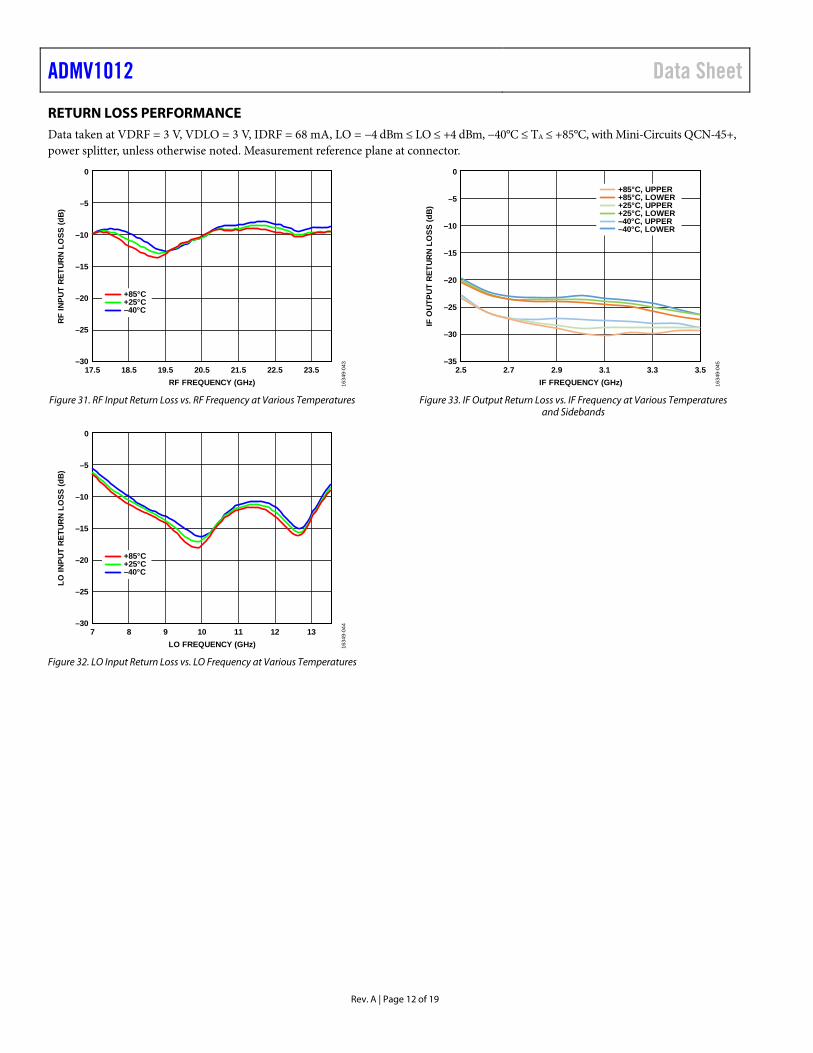
RETURN LOSS PERFORMANCE Data taken at VDRF = 3 V, VDLO = 3 V, IDRF = 68 mA, LO = −4 dBm ≤ LO ≤ +4 dBm, −40°C ≤ TA ≤ +85°C, with Mini-Circuits QCN-45+, power splitter, unless otherwise noted. Measurement reference plane at connector.
0
–30
–25
–20
–15
–10
–5
17.5 18.5 19.5 20.5 21.5 22.5 23.5
RF
INPU
T R
ETU
RN
LO
SS (d
B)
RF FREQUENCY (GHz)
+85°C+25°C–40°C
1634
9-04
3
Figure 31. RF Input Return Loss vs. RF Frequency at Various Temperatures
0
–30
–25
–20
–15
–10
–5
7 8 9 10 11 12 13
LO IN
PUT
RET
UR
N L
OSS
(dB
)
LO FREQUENCY (GHz)
+85°C+25°C–40°C
1634
9-04
4
Figure 32. LO Input Return Loss vs. LO Frequency at Various Temperatures
0
–35
–30
–25
–20
–15
–10
–5
2.5 2.7 2.9 3.1 3.3 3.5
IF O
UTP
UT
RET
UR
N L
OSS
(dB
)
IF FREQUENCY (GHz)
+85°C, UPPER+85°C, LOWER+25°C, UPPER+25°C, LOWER–40°C, UPPER–40°C, LOWER
1634
9-04
5
Figure 33. IF Output Return Loss vs. IF Frequency at Various Temperatures
and Sidebands
Data Sheet ADMV1012
Rev. A | Page 13 of 19
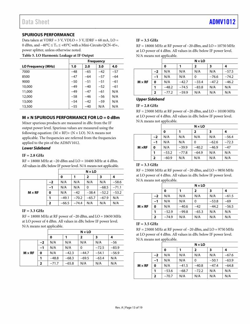
SPURIOUS PERFORMANCE Data taken at VDRF = 3 V, VDLO = 3 V, IDRF = 68 mA, LO = 0 dBm, and −40°C ≤ TA ≤ +85°C with a Mini-Circuits QCN-45+, power splitter, unless otherwise noted. Table 5. LO Harmonic Leakage at IF Output Frequency LO Frequency (MHz) 1.0 2.0 3.0 4.0 7000 −48 −65 −42 −57 8500 −47 −64 −57 −64 9000 −50 −51 −51 −61 10,000 −49 −40 −52 −61 11,000 −49 −47 −61 N/A 12,000 −58 −46 −56 N/A 13,000 −54 −42 −59 N/A 13,500 −55 −40 N/A N/A
M × N SPURIOUS PERFORMANCE FOR LO = 0 dBm Mixer spurious products are measured in dBc from the IF output power level. Spurious values are measured using the following equation: (M × RF)+ (N × LO). N/A means not applicable. The frequencies are referred from the frequencies applied to the pin of the ADMV1012. Lower Sideband
IF = 2.8 GHz RF = 18000 MHz at −20 dBm and LO = 10400 MHz at 4 dBm. All values in dBc below IF power level. N/A means not applicable. N × LO 0 1 2 3 4
M × RF
−2 N/A N/A N/A N/A −58.6
−1 N/A N/A 0 −68.5 −71.1
0 N/A −42 −38.4 −52.2 −53.2
1 −49.1 −70.2 −65.7 −67.9 N/A
2 −66.5 −74.4 N/A N/A N/A
IF = 3.3 GHz RF = 18000 MHz at RF power of −20 dBm, and LO = 10650 MHz at LO power of 4 dBm. All values in dBc below IF power level. N/A means not applicable. N × LO 0 1 2 3 4
M × RF
−2 N/A N/A N/A N/A −56
−1 N/A N/A 0 −72.5 −83.9
0 N/A −42.3 −44.7 −54.1 −56.9
1 −48.8 −68.3 −69.5 −63.4 N/A
2 −71.7 −65.8 N/A N/A N/A
IF = 3.5 GHz RF = 18000 MHz at RF power of −20 dBm, and LO = 10750 MHz at LO power of 4 dBm. All values in dBc below IF power level. N/A means not applicable. N × LO 0 1 2 3 4
M × RF
−2 N/A N/A N/A N/A −57.5
−1 N/A N/A 0 −76.6 −74.2
0 N/A −42.7 −33.4 −47.2 −46.2
1 −48.2 −74.5 −83.8 N/A N/A
2 −77.2 −59.9 N/A N/A N/A
Upper Sideband
IF = 2.8 GHz RF = 23000 MHz at RF power of −20 dBm, and LO = 10100 MHz at LO power of 4 dBm. All values in dBc below IF power level. N/A means not applicable. N × LO 0 1 2 3 4
M ×RF
−2 N/A N/A N/A N/A −56.4
−1 N/A N/A 0 −62.6 −72.3
0 N/A −39.9 −40.2 −46.9 −47
1 −53.2 −77.8 −64.9 N/A N/A
2 −60.9 N/A N/A N/A N/A
IF = 3.3 GHz RF = 23000 MHz at RF power of −20 dBm, and LO = 9850 MHz at LO power of 4 dBm. All values in dBc below IF power level. N/A means not applicable. N × LO 0 1 2 3 4
M × RF
−2 N/A N/A N/A N/A −61.5
−1 N/A N/A 0 −53.8 −69
0 N/A −40.6 −42 −44.2 −56.5
1 −52.9 −99.8 −65.3 N/A N/A
2 −74.9 N/A N/A N/A N/A
IF = 3.5 GHz RF = 23000 MHz at RF power of −20 dBm, and LO = 9750 MHz at LO power of 4 dBm. All values in dBc below IF power level. N/A means not applicable. N × LO 0 1 2 3 4
M × RF
−2 N/A N/A N/A N/A −67.6
−1 N/A N/A 0 −50.1 −63.9
0 N/A −41.5 −40.8 −47.4 −64.8
1 −53.6 −68.7 −72.2 N/A N/A
2 −70.7 N/A N/A N/A N/A

ADMV1012 Data Sheet
Rev. A | Page 14 of 19
THEORY OF OPERATION The ADMV1012 is a compact GaAs, MMIC, double sideband (DSB) downconverter in a RoHS compliant package optimized for both upper sideband and lower sideband point to point microwave radio applications operating in the 17.5 GHz to 24 GHz input frequency range. The ADMV1012 supports LO input frequencies of 7 GHz to 13.5 GHz and IF output frequencies of 2.5 GHz to 3.5 GHz.
The ADMV1012 uses a RF LNA followed by an I/Q double balanced mixer, where a driver amplifier drives the LO (see Figure 1). This combination of design, process, and packaging technology allows the functions of these subsystems to be integrated into a single die, using mature packaging and interconnection technologies to provide a high performance, low cost design with excellent electrical, mechanical, and thermal properties. In addition, the need for external components is minimized, optimizing cost and size.
LO DRIVER AMPLIFIER The LO driver amplifier takes a single LO input and doubles the frequency and amplifies it to the desired LO signal level for the mixer to operate optimally. The LO driver amplifier is self biased, and it requires only a single dc bias voltage (VDLO), which draws approximately 170 mA at 3 V under the LO drive. The LO amplitude range of −4 dBm to +4 dBm makes it compatible with the Analog Devices, Inc., wideband synthesizer portfolio without the need for an external LO driver amplifier.
MIXER The mixer is an I/Q double balanced mixer, and this mixer topology reduces the need for filtering unwanted sideband. An external 90° hybrid is required to select the upper sideband of operation. The ADMV1012 has been optimized to work with the Mini-Circuits QCN-45+ RF 90° hybrid.
LNA The LNA requires a single dc bias voltage (VDRF) and a single dc gate bias (VGRF) to operate. Starting at −1.8 V at the gate supply (VGRF), the LNA is biased at +3 V (VDRF). Then, the gate bias (VGRF) is varied until the desired LNA bias current (IDRF) is achieved. The desired LNA bias current is 68 mA at 3 V under small signal conditions.
The typical application circuit (see Figure 34) shows the necessary external components on the bias lines to eliminate any undesired stability problems for the RF amplifier and the LO amplifier.
The ADMV1012 is a much smaller alternative to hybrid style image reject converter assemblies, and it eliminates the need for wire bonding by allowing the use of surface-mount manufacturing assemblies.
The ADMV1012 downconverter comes in a compact, thermally enhanced, 4.9 mm × 4.9 mm, 32-terminal ceramic leadless chip carrier (LCC) package. The ADMV1012 operates over the −40°C to +85°C temperature range.

Data Sheet ADMV1012
Rev. A | Page 15 of 19
APPLICATIONS INFORMATION The evaluation board and typical application circuit are optimized for low-side LO (upper sideband) performance with the Mini-Circuit QCN-45+ RF 90° hybrid. Because the I/Q mixers are double balanced, the ADMV1012 can support IF frequencies from 3.5 GHz to low frequency.
TYPICAL APPLICATION CIRCUIT The typical applications circuit is shown in Figure 34. The application circuit shown has been replicated for the evaluation board circuit.
1634
9-04
9
ADMV1012AEZ
25-146-1000-92
25-146-1000-92
25-146-1000-92
25-146-1000-92
5019
5019 5019
1µF
100pF
0.01µF
100pF
QCN-45+
0.01µF
1µF
100pF
0.01µF
1µF
0Ω
0Ω
DUT
VDLO
VDRFVGRF
R4IF_OUTPUT_LSB
C9
C3
LO_INPUT
X1
C7
C10
C5
C13
C12
C11
R1IF_OUTPUT_USB
RF_INPUT
C8
LO_INPUT
RF_INPUT
VDLO
31
1427
15
3
PAD
32 30 29 28 26 25
2423
21
191817
1613129
8765
1
10
22
20
11
4
2
1
11
4 3 2
4 3 2
4 3 2
4 3 2 1
1
1 6
4
2 5
3
1
1
AGND
AGND
AGND
AGND
AGND
AGND
AGND
PORT_1
PORT_2
GND50Ω _TERM
GND
SUM_PORT
AGNDAGND AGND
AGND
PAD
NIC
VGR
FN
ICN
ICN
ICVD
RF
NIC
NIC
NICNICIF1
NICIF2
NICNICNIC
NIC
VDLO
NIC
NIC
NIC
GN
DLO
INN
IC
NICNICNICNICGNDRFINGNDNIC
Figure 34. Typical Application Circuit
ADMV1012 Data Sheet
Rev. A | Page 16 of 19
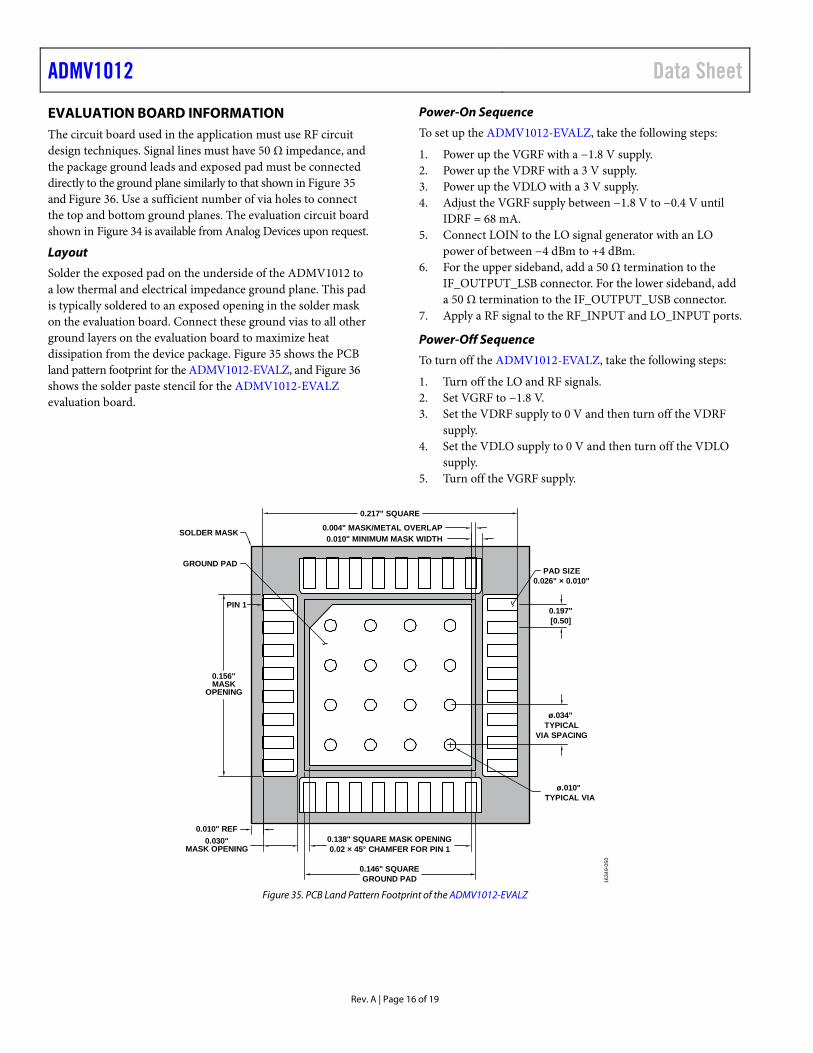
EVALUATION BOARD INFORMATION The circuit board used in the application must use RF circuit design techniques. Signal lines must have 50 Ω impedance, and the package ground leads and exposed pad must be connected directly to the ground plane similarly to that shown in Figure 35 and Figure 36. Use a sufficient number of via holes to connect the top and bottom ground planes. The evaluation circuit board shown in Figure 34 is available from Analog Devices upon request.
Layout
Solder the exposed pad on the underside of the ADMV1012 to a low thermal and electrical impedance ground plane. This pad is typically soldered to an exposed opening in the solder mask on the evaluation board. Connect these ground vias to all other ground layers on the evaluation board to maximize heat dissipation from the device package. Figure 35 shows the PCB land pattern footprint for the ADMV1012-EVALZ, and Figure 36 shows the solder paste stencil for the ADMV1012-EVALZ evaluation board.
Power-On Sequence
To set up the ADMV1012-EVALZ, take the following steps:
1. Power up the VGRF with a −1.8 V supply. 2. Power up the VDRF with a 3 V supply. 3. Power up the VDLO with a 3 V supply. 4. Adjust the VGRF supply between −1.8 V to −0.4 V until
IDRF = 68 mA. 5. Connect LOIN to the LO signal generator with an LO
power of between −4 dBm to +4 dBm. 6. For the upper sideband, add a 50 Ω termination to the
IF_OUTPUT_LSB connector. For the lower sideband, add a 50 Ω termination to the IF_OUTPUT_USB connector.
7. Apply a RF signal to the RF_INPUT and LO_INPUT ports.
Power-Off Sequence
To turn off the ADMV1012-EVALZ, take the following steps:
1. Turn off the LO and RF signals. 2. Set VGRF to −1.8 V. 3. Set the VDRF supply to 0 V and then turn off the VDRF
supply. 4. Set the VDLO supply to 0 V and then turn off the VDLO
supply. 5. Turn off the VGRF supply.
0.138" SQUARE MASK OPENING0.02 × 45° CHAMFER FOR PIN 1
0.197"[0.50]
PAD SIZE0.026" × 0.010"
0.217" SQUARE
0.004" MASK/METAL OVERLAP0.010" MINIMUM MASK WIDTH
0.010" REF0.030"
MASK OPENING
0.156"MASK
OPENING
PIN 1
GROUND PAD
SOLDER MASK
0.146" SQUAREGROUND PAD
ø.010"TYPICAL VIA
ø.034"TYPICAL
VIA SPACING
1634
9-05
0
Figure 35. PCB Land Pattern Footprint of the ADMV1012-EVALZ

Data Sheet ADMV1012
Rev. A | Page 17 of 19
0.219SQUARE
0.017
0.017
0.027TYP
0.010TYP
0.0197TYP
R0.0040 TYP132 PLCS
0.132SQUARE
1634
9-05
1
Figure 36. Solder Paste Stencil of the ADMV1012-EVALZ
1634
9-05
2
NOTES1. NOT ALL COMPONENTS OR BIAS LINES ARE USED ON THE EVALUATION BOARD.
Figure 37. ADMV1012-EVALZ Evaluation Board Top Layer

ADMV1012 Data Sheet
Rev. A | Page 18 of 19
BILL OF MATERIALS
Table 6. Qty. Component Description Manufacturer/Part No. 1 Evaluation board PCB Analog Devices, Supplied/042365 4 C5, C7, C12 100 pF, high temperature, multilayer
ceramic capacitors, NP0, 0402 TDK/C1005NP01H101J050BA
4 C8, C10, C11 0.01 µF ceramic capacitors, X7R, 0402 Murata Manufacturing/GRM155R71E103KA01D 4 C3, C9, C13 1 µF ceramic capacitors, X5R, 0603 Murata Manufacturing/GRM188R61E105KA12D 7 GND, VDLO, VDRF, VGRF CONN-PCB test points, compact mini,
CNKEY5019 Keystone Electronics Corporation/5019.00
4 LO_INPUT, RF_INPUT, IF_OUTPUT_LSB, IF_OUTPUT_USB
CONN-PCB, SMA K_SRI-NS, CNSMAL460W295H156
SRI CONNECTOR GAGE/25-146-1000-92
2 R1, R4 0 Ω resistor chips, SMD, JMPR, 0402 Panasonic/ERJ-2GE0R00X 1 X1 XFMR, power splitter/combiner,
2500 MHz to 4500 MHz, TSML126W63H42
Mini-Circuits/QCN-45+
1 Device under test (DUT) 17.5 GHz to 24 GHz, GaAs, MMIC, I/Q downconverter
Analog Devices Supplied/ADMV1012AEZ
1 Heatsink Heatsink Analog Devices Supplied/104365
Data Sheet ADMV1012
Rev. A | Page 19 of 19
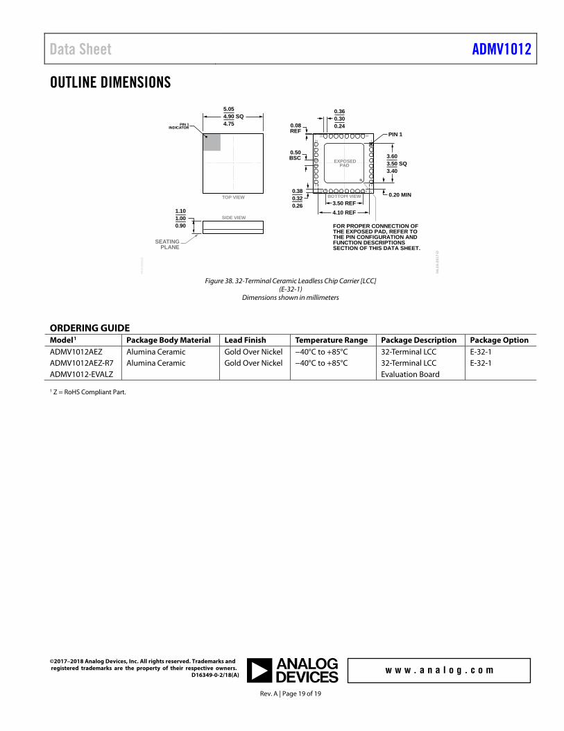
OUTLINE DIMENSIONS
16
0.50BSC
3.50 REF0.20 MINBOTTOM VIEWTOP VIEW
SIDE VIEW
1
32
9
17
2425
8
FOR PROPER CONNECTION OFTHE EXPOSED PAD, REFER TOTHE PIN CONFIGURATION ANDFUNCTION DESCRIPTIONSSECTION OF THIS DATA SHEET.
04-2
4-20
17-D
0.360.300.24
EXPOSEDPAD
PKG
-004
843
PIN 1INDICATOR
5.054.90 SQ4.75
4.10 REF1.101.000.90
0.380.320.26
3.603.50 SQ3.40
PIN 10.08REF
SEATINGPLANE
Figure 38. 32-Terminal Ceramic Leadless Chip Carrier [LCC]
(E-32-1) Dimensions shown in millimeters
ORDERING GUIDE Model1 Package Body Material Lead Finish Temperature Range Package Description Package Option ADMV1012AEZ Alumina Ceramic Gold Over Nickel −40°C to +85°C 32-Terminal LCC E-32-1 ADMV1012AEZ-R7 Alumina Ceramic Gold Over Nickel −40°C to +85°C 32-Terminal LCC E-32-1 ADMV1012-EVALZ Evaluation Board 1 Z = RoHS Compliant Part.
©2017–2018 Analog Devices, Inc. All rights reserved. Trademarks and registered trademarks are the property of their respective owners. D16349-0-2/18(A)


![30.0-36.0 GHz GaAs MMIC Power Amplifier - MACOM · Page 4 of 8 S-Parameters (On-Wafer1) 30.0-36.0 GHz GaAs MMIC Power Amplifier P1017-BD Note [1] S-Parameters – Measurements are](https://img.pdfslide.us/doc/110x75/5e77abe896af705b671d3692/300-360-ghz-gaas-mmic-power-amplifier-macom-page-4-of-8-s-parameters-on-wafer1.jpg)