Embed Size (px)
Citation preview
Instruction Manual
1705A
Spectrum Monitor (SN B040000 and Above)
070-8222-08
Warning
The servicing instructions are for use by qualifiedpersonnel only. To avoid personal injury, do notperform any servicing unless you are qualified todo so. Refer to all safety summaries prior toperforming service.
www.tektronix.com
Test Equipment Depot - 800.517.8431 - 99 Washington Street Melrose, MA 02176 - FAX 781.665.0780 - TestEquipmentDepot.com
1705A Spectrum Monitor i
Table of Contents
General Safety Summary ix. . . . . . . . . . . . . . . . . . . . . . . . . . . . . . . . . . . . . . . . . . . . . .
Service Safety Summary xi. . . . . . . . . . . . . . . . . . . . . . . . . . . . . . . . . . . . . . . . . . . . . .
Preface xiii. . . . . . . . . . . . . . . . . . . . . . . . . . . . . . . . . . . . . . . . . . . . . . . . . . . . . . . . . . . . .Contacting Tektronix xv
Introduction
Section 1 Introduction 1--1. . . . . . . . . . . . . . . . . . . . . . . . . . . . . . . . . . . . . . . . . . . . . . . .Typical Configurations 1--1. . . . . . . . . . . . . . . . . . . . . . . . . . . . . . . . . . . . . . . . . . . . . . . . . . .Options 1--2. . . . . . . . . . . . . . . . . . . . . . . . . . . . . . . . . . . . . . . . . . . . . . . . . . . . . . . . . . . . . . .Accessories 1--2. . . . . . . . . . . . . . . . . . . . . . . . . . . . . . . . . . . . . . . . . . . . . . . . . . . . . . . . . . . .
Standard Accessories 1--2. . . . . . . . . . . . . . . . . . . . . . . . . . . . . . . . . . . . . . . . . . . . . . . . .Optional Accessories 1--3. . . . . . . . . . . . . . . . . . . . . . . . . . . . . . . . . . . . . . . . . . . . . . . . .
Safety Information 1--3. . . . . . . . . . . . . . . . . . . . . . . . . . . . . . . . . . . . . . . . . . . . . . . . . . . . . .ELECTRICAL SPECIFICATION 1--4. . . . . . . . . . . . . . . . . . . . . . . . . . . . . . . . . . . . . . . . . .APPLICATIONS 1--9. . . . . . . . . . . . . . . . . . . . . . . . . . . . . . . . . . . . . . . . . . . . . . . . . . . . . . . .
Locating Satellites 1--9. . . . . . . . . . . . . . . . . . . . . . . . . . . . . . . . . . . . . . . . . . . . . . . . . . .Satellite Footprints 1--10. . . . . . . . . . . . . . . . . . . . . . . . . . . . . . . . . . . . . . . . . . . . . . . . . . .
Using the 1705A for Satellite Communication 1--11. . . . . . . . . . . . . . . . . . . . . . . . . . . . . . . .L--Band Input Signals 1--12. . . . . . . . . . . . . . . . . . . . . . . . . . . . . . . . . . . . . . . . . . . . . . . . . . . .Zeroing in on a Satellite 1--13. . . . . . . . . . . . . . . . . . . . . . . . . . . . . . . . . . . . . . . . . . . . . . . . . .
Locating the Satellite 1--13. . . . . . . . . . . . . . . . . . . . . . . . . . . . . . . . . . . . . . . . . . . . . . . . .Identifying the Satellite 1--13. . . . . . . . . . . . . . . . . . . . . . . . . . . . . . . . . . . . . . . . . . . . . . .Finding The Correct Transponder 1--15. . . . . . . . . . . . . . . . . . . . . . . . . . . . . . . . . . . . . . .Optimize Signal Strength 1--15. . . . . . . . . . . . . . . . . . . . . . . . . . . . . . . . . . . . . . . . . . . . . .Looking at Exciters with the 70 MHz Input 1--16. . . . . . . . . . . . . . . . . . . . . . . . . . . . . . .
Miscellaneous Uses for the 1705A 1--17. . . . . . . . . . . . . . . . . . . . . . . . . . . . . . . . . . . . . . . . . .
Operating Instructions
Section 2 Operating Instructions 2--1. . . . . . . . . . . . . . . . . . . . . . . . . . . . . . . . . . . . . . .Front-panel Controls and Indicators 2--1. . . . . . . . . . . . . . . . . . . . . . . . . . . . . . . . . . . . . . . . .
FILTER 2--1. . . . . . . . . . . . . . . . . . . . . . . . . . . . . . . . . . . . . . . . . . . . . . . . . . . . . . . . . . . .INPUT 2--1. . . . . . . . . . . . . . . . . . . . . . . . . . . . . . . . . . . . . . . . . . . . . . . . . . . . . . . . . . . .SWEEP 2--2. . . . . . . . . . . . . . . . . . . . . . . . . . . . . . . . . . . . . . . . . . . . . . . . . . . . . . . . . . . .DISPLAY 2--3. . . . . . . . . . . . . . . . . . . . . . . . . . . . . . . . . . . . . . . . . . . . . . . . . . . . . . . . . .POSITION 2--4. . . . . . . . . . . . . . . . . . . . . . . . . . . . . . . . . . . . . . . . . . . . . . . . . . . . . . . . .POWER 2--4. . . . . . . . . . . . . . . . . . . . . . . . . . . . . . . . . . . . . . . . . . . . . . . . . . . . . . . . . . .
Rear--Panel Connectors 2--4. . . . . . . . . . . . . . . . . . . . . . . . . . . . . . . . . . . . . . . . . . . . . . . . . . .INPUTS 2--4. . . . . . . . . . . . . . . . . . . . . . . . . . . . . . . . . . . . . . . . . . . . . . . . . . . . . . . . . . .POWER 2--5. . . . . . . . . . . . . . . . . . . . . . . . . . . . . . . . . . . . . . . . . . . . . . . . . . . . . . . . . . .
Powering--up 2--6. . . . . . . . . . . . . . . . . . . . . . . . . . . . . . . . . . . . . . . . . . . . . . . . . . . . . . . . . . .Measurement Graticule 2--7. . . . . . . . . . . . . . . . . . . . . . . . . . . . . . . . . . . . . . . . . . . . . . . . . . .
Table of Contents
ii 1705A Spectrum Monitor
Vertical Scales 2--7. . . . . . . . . . . . . . . . . . . . . . . . . . . . . . . . . . . . . . . . . . . . . . . . . . . . . .Horizontal Scales 2--9. . . . . . . . . . . . . . . . . . . . . . . . . . . . . . . . . . . . . . . . . . . . . . . . . . . .
Center Frequency Readout 2--11. . . . . . . . . . . . . . . . . . . . . . . . . . . . . . . . . . . . . . . . . . . . . . . .Customizing Frequency Readout 2--14. . . . . . . . . . . . . . . . . . . . . . . . . . . . . . . . . . . . . . . . . . .
Turning On or Off Readout 2--14. . . . . . . . . . . . . . . . . . . . . . . . . . . . . . . . . . . . . . . . . . . .Changing Readout Position 2--14. . . . . . . . . . . . . . . . . . . . . . . . . . . . . . . . . . . . . . . . . . . .Changing Readout Frequency 2--15. . . . . . . . . . . . . . . . . . . . . . . . . . . . . . . . . . . . . . . . . .Test Mode 2--17. . . . . . . . . . . . . . . . . . . . . . . . . . . . . . . . . . . . . . . . . . . . . . . . . . . . . . . . . .
Locating Ku--Band Satellites 2--17. . . . . . . . . . . . . . . . . . . . . . . . . . . . . . . . . . . . . . . . . . . . . .Basic Operating Procedure 2--17. . . . . . . . . . . . . . . . . . . . . . . . . . . . . . . . . . . . . . . . . . . .
Installation
Section 3 Installation 3--1. . . . . . . . . . . . . . . . . . . . . . . . . . . . . . . . . . . . . . . . . . . . . . . . .Packaging 3--1. . . . . . . . . . . . . . . . . . . . . . . . . . . . . . . . . . . . . . . . . . . . . . . . . . . . . . . . . .
Electrical Installation 3--1. . . . . . . . . . . . . . . . . . . . . . . . . . . . . . . . . . . . . . . . . . . . . . . . . . . .Power Source 3--1. . . . . . . . . . . . . . . . . . . . . . . . . . . . . . . . . . . . . . . . . . . . . . . . . . . . . . .Mains Frequency and Voltage Ranges 3--1. . . . . . . . . . . . . . . . . . . . . . . . . . . . . . . . . . . .+18 Volts For Block Down Converter 3--1. . . . . . . . . . . . . . . . . . . . . . . . . . . . . . . . . . . .Operating Options 3--2. . . . . . . . . . . . . . . . . . . . . . . . . . . . . . . . . . . . . . . . . . . . . . . . . . .
Mechanical Installation 3--2. . . . . . . . . . . . . . . . . . . . . . . . . . . . . . . . . . . . . . . . . . . . . . . . . . .Cabinet Options 3--2. . . . . . . . . . . . . . . . . . . . . . . . . . . . . . . . . . . . . . . . . . . . . . . . . . . . .Cabinetizing 3--4. . . . . . . . . . . . . . . . . . . . . . . . . . . . . . . . . . . . . . . . . . . . . . . . . . . . . . . .Rack Adapter 3--5. . . . . . . . . . . . . . . . . . . . . . . . . . . . . . . . . . . . . . . . . . . . . . . . . . . . . . .Custom Installation 3--8. . . . . . . . . . . . . . . . . . . . . . . . . . . . . . . . . . . . . . . . . . . . . . . . . .
Theory of Operation
Section 4 Theory of Operation 4--1. . . . . . . . . . . . . . . . . . . . . . . . . . . . . . . . . . . . . . . . .Overview 4--1. . . . . . . . . . . . . . . . . . . . . . . . . . . . . . . . . . . . . . . . . . . . . . . . . . . . . . . . . . . . . .Block Diagram 4--1. . . . . . . . . . . . . . . . . . . . . . . . . . . . . . . . . . . . . . . . . . . . . . . . . . . . . . . . .
RF Input Circuits (Diagram 1) 4--1. . . . . . . . . . . . . . . . . . . . . . . . . . . . . . . . . . . . . . . . . .IF Amplifier Circuits (Diagram 2) 4--2. . . . . . . . . . . . . . . . . . . . . . . . . . . . . . . . . . . . . . .Sweep Generator Circuits (Diagram 3) 4--2. . . . . . . . . . . . . . . . . . . . . . . . . . . . . . . . . . .Deflection Amplifiers (Diagram 4) 4--3. . . . . . . . . . . . . . . . . . . . . . . . . . . . . . . . . . . . . .Microprocessor (Diagram 5) 4--3. . . . . . . . . . . . . . . . . . . . . . . . . . . . . . . . . . . . . . . . . . .Front Panel (Diagram 6) 4--3. . . . . . . . . . . . . . . . . . . . . . . . . . . . . . . . . . . . . . . . . . . . . .Low Voltage Power Supply (Diagram 7) 4--3. . . . . . . . . . . . . . . . . . . . . . . . . . . . . . . . . .High Voltage (Diagram 8) 4--4. . . . . . . . . . . . . . . . . . . . . . . . . . . . . . . . . . . . . . . . . . . . .
RF InputDiagram 1 4--4. . . . . . . . . . . . . . . . . . . . . . . . . . . . . . . . . . . . . . . . . . . . . . . . . .
L--Band Input 4--4. . . . . . . . . . . . . . . . . . . . . . . . . . . . . . . . . . . . . . . . . . . . . . . . . . . . . . .70 MHz Input 4--4. . . . . . . . . . . . . . . . . . . . . . . . . . . . . . . . . . . . . . . . . . . . . . . . . . . . . . .70 MHz Local Oscillator 4--5. . . . . . . . . . . . . . . . . . . . . . . . . . . . . . . . . . . . . . . . . . . . . .
IF AmplifierDiagram 2 4--5. . . . . . . . . . . . . . . . . . . . . . . . . . . . . . . . . . . . . . . . . . . . . . . . . .
2nd Local Oscillator 4--5. . . . . . . . . . . . . . . . . . . . . . . . . . . . . . . . . . . . . . . . . . . . . . . . . .Input Filter, Mixer, and IF Amplifier 4--6. . . . . . . . . . . . . . . . . . . . . . . . . . . . . . . . . . . . .Resolution Filter and Log Detector 4--6. . . . . . . . . . . . . . . . . . . . . . . . . . . . . . . . . . . . . .
Sweep GeneratorDiagram 3 4--7. . . . . . . . . . . . . . . . . . . . . . . . . . . . . . . . . . . . . . . . . . . . . . . . . .
Table of Contents
1705A Spectrum Monitor iii
Ramp Generator 4--7. . . . . . . . . . . . . . . . . . . . . . . . . . . . . . . . . . . . . . . . . . . . . . . . . . . . .Gain Control (SPAN/DIV) 4--7. . . . . . . . . . . . . . . . . . . . . . . . . . . . . . . . . . . . . . . . . . . . .Sweep Shapers 4--7. . . . . . . . . . . . . . . . . . . . . . . . . . . . . . . . . . . . . . . . . . . . . . . . . . . . . .Bright--Up Generator 4--8. . . . . . . . . . . . . . . . . . . . . . . . . . . . . . . . . . . . . . . . . . . . . . . . .Z--Axis Control 4--9. . . . . . . . . . . . . . . . . . . . . . . . . . . . . . . . . . . . . . . . . . . . . . . . . . . . .
Deflection AmplifiersDiagram 4 4--9. . . . . . . . . . . . . . . . . . . . . . . . . . . . . . . . . . . . . . . . . . . . . . . . . .
Buffers 4--9. . . . . . . . . . . . . . . . . . . . . . . . . . . . . . . . . . . . . . . . . . . . . . . . . . . . . . . . . . . .Vertical Deflection Amplifier 4--10. . . . . . . . . . . . . . . . . . . . . . . . . . . . . . . . . . . . . . . . . .Horizontal Deflection Amplifier 4--10. . . . . . . . . . . . . . . . . . . . . . . . . . . . . . . . . . . . . . . .
MicroprocessorDiagram 5 4--11. . . . . . . . . . . . . . . . . . . . . . . . . . . . . . . . . . . . . . . . . . . . . . . . . .
Microprocessor 4--11. . . . . . . . . . . . . . . . . . . . . . . . . . . . . . . . . . . . . . . . . . . . . . . . . . . . . .Readout 4--12. . . . . . . . . . . . . . . . . . . . . . . . . . . . . . . . . . . . . . . . . . . . . . . . . . . . . . . . . . .Trace Rotate 4--12. . . . . . . . . . . . . . . . . . . . . . . . . . . . . . . . . . . . . . . . . . . . . . . . . . . . . . . .Graticule Lights 4--12. . . . . . . . . . . . . . . . . . . . . . . . . . . . . . . . . . . . . . . . . . . . . . . . . . . . .
Front PanelDiagram 6 4--12. . . . . . . . . . . . . . . . . . . . . . . . . . . . . . . . . . . . . . . . . . . . . . . . . .
Indicators, Controls, and Switches 4--12. . . . . . . . . . . . . . . . . . . . . . . . . . . . . . . . . . . . . .+18 Volt Supply 4--13. . . . . . . . . . . . . . . . . . . . . . . . . . . . . . . . . . . . . . . . . . . . . . . . . . . . .
Low Voltage Power SupplyDiagram 7 4--14. . . . . . . . . . . . . . . . . . . . . . . . . . . . . . . . . . . . . . . . . . . . . . . . . .
Line Rectifier and Filter 4--15. . . . . . . . . . . . . . . . . . . . . . . . . . . . . . . . . . . . . . . . . . . . . .Pulse Width Modulator 4--15. . . . . . . . . . . . . . . . . . . . . . . . . . . . . . . . . . . . . . . . . . . . . . .Output Filters 4--16. . . . . . . . . . . . . . . . . . . . . . . . . . . . . . . . . . . . . . . . . . . . . . . . . . . . . . .Error Amplifier 4--16. . . . . . . . . . . . . . . . . . . . . . . . . . . . . . . . . . . . . . . . . . . . . . . . . . . . .Feedback Transformer Driver and Peak Detector 4--16. . . . . . . . . . . . . . . . . . . . . . . . . . .Output Under-Voltage Shutdown 4--16. . . . . . . . . . . . . . . . . . . . . . . . . . . . . . . . . . . . . . . .
High Voltage Power SupplyDiagram 8 4--17. . . . . . . . . . . . . . . . . . . . . . . . . . . . . . . . . . . . . . . . . . . . . . . . . .
HV Osc and Error Amp 4--17. . . . . . . . . . . . . . . . . . . . . . . . . . . . . . . . . . . . . . . . . . . . . . .Power Supply Outputs 4--18. . . . . . . . . . . . . . . . . . . . . . . . . . . . . . . . . . . . . . . . . . . . . . . .Focus Amplifier 4--18. . . . . . . . . . . . . . . . . . . . . . . . . . . . . . . . . . . . . . . . . . . . . . . . . . . . .Grid Drive Circuit 4--18. . . . . . . . . . . . . . . . . . . . . . . . . . . . . . . . . . . . . . . . . . . . . . . . . . .Z-Axis Amplifier 4--18. . . . . . . . . . . . . . . . . . . . . . . . . . . . . . . . . . . . . . . . . . . . . . . . . . . .
Checks and Adjustments
Section 5 Checks And Adjustments 5--1. . . . . . . . . . . . . . . . . . . . . . . . . . . . . . . . . . . . .Recommended Equipment List 5--1. . . . . . . . . . . . . . . . . . . . . . . . . . . . . . . . . . . . . . . . . . . . .
Electrical Instruments 5--1. . . . . . . . . . . . . . . . . . . . . . . . . . . . . . . . . . . . . . . . . . . . . . . .Auxiliary Equipment 5--2. . . . . . . . . . . . . . . . . . . . . . . . . . . . . . . . . . . . . . . . . . . . . . . . .
Performance Check 5--3. . . . . . . . . . . . . . . . . . . . . . . . . . . . . . . . . . . . . . . . . . . . . . . . . . . . . .Short-Form Procedure 5--3. . . . . . . . . . . . . . . . . . . . . . . . . . . . . . . . . . . . . . . . . . . . . . . .Long Form Procedure 5--5. . . . . . . . . . . . . . . . . . . . . . . . . . . . . . . . . . . . . . . . . . . . . . . .
Adjustment Procedure 5--17. . . . . . . . . . . . . . . . . . . . . . . . . . . . . . . . . . . . . . . . . . . . . . . . . . . .
Table of Contents
iv 1705A Spectrum Monitor
Short--Form Procedure 5--17. . . . . . . . . . . . . . . . . . . . . . . . . . . . . . . . . . . . . . . . . . . . . . . .Long Form Procedure 5--18. . . . . . . . . . . . . . . . . . . . . . . . . . . . . . . . . . . . . . . . . . . . . . . .
Maintenance 6- - 1. . . . . . . . . . . . . . . . . . . . . . . . . . . . . . . . . . . . . . . . . .
Section 6 Maintenance 6--1. . . . . . . . . . . . . . . . . . . . . . . . . . . . . . . . . . . . . . . . . . . . . . . .PREVENTIVE MAINTENANCE 6--1. . . . . . . . . . . . . . . . . . . . . . . . . . . . . . . . . . . . . . . . . .
Cleaning 6--1. . . . . . . . . . . . . . . . . . . . . . . . . . . . . . . . . . . . . . . . . . . . . . . . . . . . . . . . . . .Visual Inspection 6--2. . . . . . . . . . . . . . . . . . . . . . . . . . . . . . . . . . . . . . . . . . . . . . . . . . . .Static--Sensitive Components 6--2. . . . . . . . . . . . . . . . . . . . . . . . . . . . . . . . . . . . . . . . . .Performance Checks and Readjustments 6--3. . . . . . . . . . . . . . . . . . . . . . . . . . . . . . . . . .
TROUBLESHOOTING 6--3. . . . . . . . . . . . . . . . . . . . . . . . . . . . . . . . . . . . . . . . . . . . . . . . . .Diagnostic Routines 6--4. . . . . . . . . . . . . . . . . . . . . . . . . . . . . . . . . . . . . . . . . . . . . . . . . . . . .
Memory Test 6--5. . . . . . . . . . . . . . . . . . . . . . . . . . . . . . . . . . . . . . . . . . . . . . . . . . . . . . .DAC Test 6--7. . . . . . . . . . . . . . . . . . . . . . . . . . . . . . . . . . . . . . . . . . . . . . . . . . . . . . . . . .LED and Key Tests 6--8. . . . . . . . . . . . . . . . . . . . . . . . . . . . . . . . . . . . . . . . . . . . . . . . . .
Troubleshooting Aids 6--8. . . . . . . . . . . . . . . . . . . . . . . . . . . . . . . . . . . . . . . . . . . . . . . . . . . .Foldout Pages 6--8. . . . . . . . . . . . . . . . . . . . . . . . . . . . . . . . . . . . . . . . . . . . . . . . . . . . . . .Parts Lists 6--9. . . . . . . . . . . . . . . . . . . . . . . . . . . . . . . . . . . . . . . . . . . . . . . . . . . . . . . . . .Major Assembly Interconnection 6--10. . . . . . . . . . . . . . . . . . . . . . . . . . . . . . . . . . . . . . . .General Troubleshooting Techniques 6--10. . . . . . . . . . . . . . . . . . . . . . . . . . . . . . . . . . . .
Power Supply Troubleshooting Procedure 6--12. . . . . . . . . . . . . . . . . . . . . . . . . . . . . . . . . . . .Introduction 6--12. . . . . . . . . . . . . . . . . . . . . . . . . . . . . . . . . . . . . . . . . . . . . . . . . . . . . . . .Low Volts Supply 6--13. . . . . . . . . . . . . . . . . . . . . . . . . . . . . . . . . . . . . . . . . . . . . . . . . . . .High Volts Supply 6--15. . . . . . . . . . . . . . . . . . . . . . . . . . . . . . . . . . . . . . . . . . . . . . . . . . .
CORRECTIVE MAINTENANCE 6--18. . . . . . . . . . . . . . . . . . . . . . . . . . . . . . . . . . . . . . . . . .Obtaining Replacement Parts 6--18. . . . . . . . . . . . . . . . . . . . . . . . . . . . . . . . . . . . . . . . . . . . . .
Test Selected Components 6--18. . . . . . . . . . . . . . . . . . . . . . . . . . . . . . . . . . . . . . . . . . . . .Mechanical Disassembly/Assembly 6--19. . . . . . . . . . . . . . . . . . . . . . . . . . . . . . . . . . . . . . . . .
Bezel Removal 6--19. . . . . . . . . . . . . . . . . . . . . . . . . . . . . . . . . . . . . . . . . . . . . . . . . . . . . .Graticule Light Removal and Replacement 6--20. . . . . . . . . . . . . . . . . . . . . . . . . . . . . . .Removal of the CRT 6--21. . . . . . . . . . . . . . . . . . . . . . . . . . . . . . . . . . . . . . . . . . . . . . . . .Replacing the CRT 6--21. . . . . . . . . . . . . . . . . . . . . . . . . . . . . . . . . . . . . . . . . . . . . . . . . . .Removal of the Rear Panel 6--22. . . . . . . . . . . . . . . . . . . . . . . . . . . . . . . . . . . . . . . . . . . .Removal of Front--Panel Assembly 6--22. . . . . . . . . . . . . . . . . . . . . . . . . . . . . . . . . . . . . .Removing the L--Band Tuner 6--23. . . . . . . . . . . . . . . . . . . . . . . . . . . . . . . . . . . . . . . . . .Removing the 70 MHz Tuner 6--24. . . . . . . . . . . . . . . . . . . . . . . . . . . . . . . . . . . . . . . . . .Removal and Replacement of the Main Board 6--24. . . . . . . . . . . . . . . . . . . . . . . . . . . . .Removal and Replacement of the Power Supply Board 6--25. . . . . . . . . . . . . . . . . . . . . .Removing the LNB Power Supply Board 6--26. . . . . . . . . . . . . . . . . . . . . . . . . . . . . . . . .
REPACKAGING 6--27. . . . . . . . . . . . . . . . . . . . . . . . . . . . . . . . . . . . . . . . . . . . . . . . . . . . . . . .
Options
Section 7 Options 7--1. . . . . . . . . . . . . . . . . . . . . . . . . . . . . . . . . . . . . . . . . . . . . . . . . . . .Options 7--1. . . . . . . . . . . . . . . . . . . . . . . . . . . . . . . . . . . . . . . . . . . . . . . . . . . . . . . . . . . . . . .Field Upgrade Kits 7--1. . . . . . . . . . . . . . . . . . . . . . . . . . . . . . . . . . . . . . . . . . . . . . . . . . . . . .ORDERING 7--2. . . . . . . . . . . . . . . . . . . . . . . . . . . . . . . . . . . . . . . . . . . . . . . . . . . . . . . . . . .
Table of Contents
1705A Spectrum Monitor v
Replaceable Electrical Parts
Section 8 Replaceable Electrical Parts 8--1. . . . . . . . . . . . . . . . . . . . . . . . . . . . . . . . . . .Parts Ordering Information 8--1. . . . . . . . . . . . . . . . . . . . . . . . . . . . . . . . . . . . . . . . . . . . . . . .Using the Replaceable Electrical Parts List 8--1. . . . . . . . . . . . . . . . . . . . . . . . . . . . . . . . . . .
Cross Index--Mfr. Code Number to Manufacturer 8--1. . . . . . . . . . . . . . . . . . . . . . . . . . .Abbreviations 8--1. . . . . . . . . . . . . . . . . . . . . . . . . . . . . . . . . . . . . . . . . . . . . . . . . . . . . . .List of Assemblies 8--1. . . . . . . . . . . . . . . . . . . . . . . . . . . . . . . . . . . . . . . . . . . . . . . . . . .
Column Descriptions 8--2. . . . . . . . . . . . . . . . . . . . . . . . . . . . . . . . . . . . . . . . . . . . . . . . . . . . .Component No. (Column 1) 8--2. . . . . . . . . . . . . . . . . . . . . . . . . . . . . . . . . . . . . . . . .
Tektronix Part No. (Column 2) 8--2. . . . . . . . . . . . . . . . . . . . . . . . . . . . . . . . . . . . . . . . .Serial/Assembly No. (Column 3 and 4) 8--2. . . . . . . . . . . . . . . . . . . . . . . . . . . . . . . . . . .Name and Description (Column 5) 8--2. . . . . . . . . . . . . . . . . . . . . . . . . . . . . . . . . . . . . .
Mfr. Code (Column 6) 8--2. . . . . . . . . . . . . . . . . . . . . . . . . . . . . . . . . . . . . . . .Mfr. Part No. (Column 7) 8--2. . . . . . . . . . . . . . . . . . . . . . . . . . . . . . . . . . . . . . . . . . . . . .
Diagrams/Circuit Board Illustrations
Replaceable Mechanical Parts
Section 10 Replaceable Mechanical Parts 10--1. . . . . . . . . . . . . . . . . . . . . . . . . . . . . . . .Parts Ordering Information 10--1. . . . . . . . . . . . . . . . . . . . . . . . . . . . . . . . . . . . . . . . . . . . . . . .Using the Replaceable Mechanical Parts List 10--1. . . . . . . . . . . . . . . . . . . . . . . . . . . . . . . . .
Table of Contents
vi 1705A Spectrum Monitor
List of Figures
Figure 1-1: 1705A used to locate satellites and determine maximum signal level 1--2. . . . . . . . .
Figure 1-2: Relationship of a communications satellite to earth 1--9. . . . . . . . . . . . . . . . . . . . . . .
Figure 1-3: Angle A (the difference at a specific latitude between the angle to the sunand the angle to a satellite) 1--10. . . . . . . . . . . . . . . . . . . . . . . . . . . . . . . . . . . . . . . . .
Figure 1-4: Sample longitudinal map of the Ku-Band satellites 1--11. . . . . . . . . . . . . . . . . . . . . . .
Figure 1-5: The western spot beam footprint for one Ku-Band satellite 1--12. . . . . . . . . . . . . . . . .
Figure 1-6: A computer representation of the 1705A display showing the 12.198 GHzhorizontally polarized telemetry beacon on the SATCOM K2 satellite 1--14. . . . . . . .
Figure 1-7: Transponder assignments for a typical Ku--Band, 16--transponder satellitethat employs alternate polarization 1--15. . . . . . . . . . . . . . . . . . . . . . . . . . . . . . . . . . . .
Figure 1-8: Simulation of a 1705A FULL SPAN/DIV display 1--16. . . . . . . . . . . . . . . . . . . . . . .
Figure 1-9: Up link Video Exciter, Up converter, and High Power Amplifier (HPA) showinghow to hook up a 1705A Spectrum Monitor to look at the Video Exciter output 1--17
Figure 1-10: 1705A hooked up to look at either the output of the Video Exciter (70 MHz)or the Receiver Input (L-Band) 1--18. . . . . . . . . . . . . . . . . . . . . . . . . . . . . . . . . . . . . . .
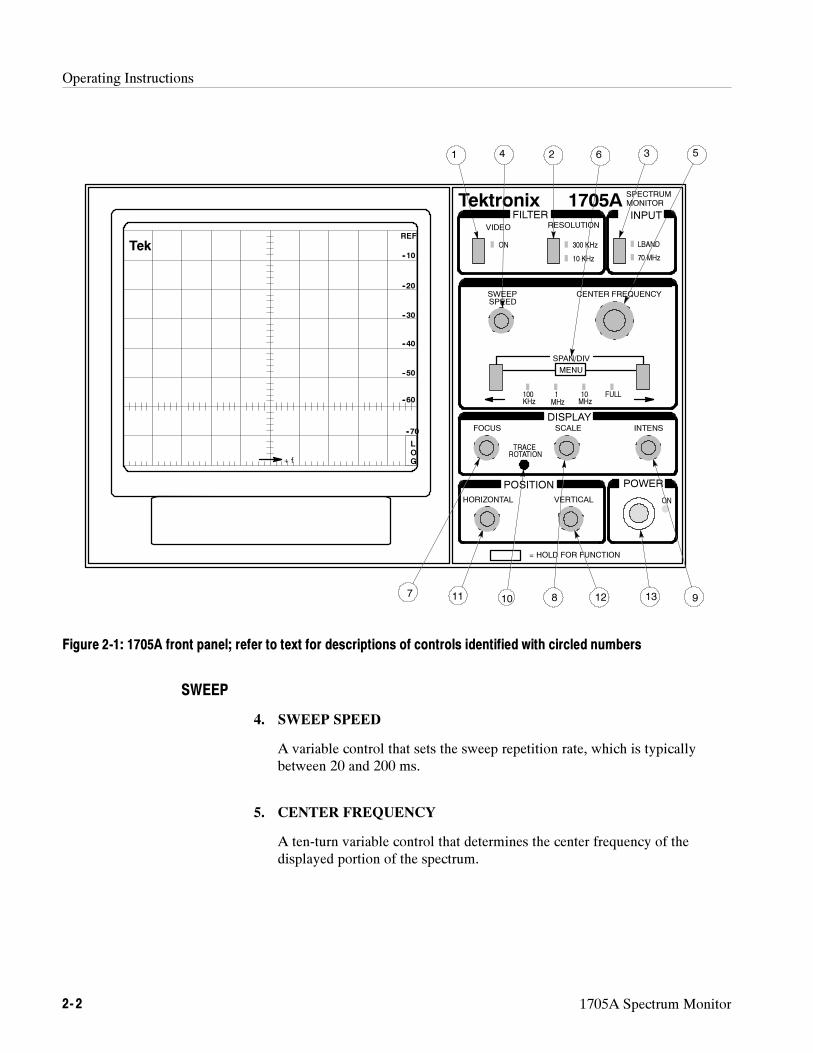
Figure 2-1: 1705A front panel 2--2. . . . . . . . . . . . . . . . . . . . . . . . . . . . . . . . . . . . . . . . . . . . . . . . .
Figure 2-2: 1705A rear panel controls and connectors 2--5. . . . . . . . . . . . . . . . . . . . . . . . . . . . . .
Figure 2-3: 1705A display when powered up in L-BAND and FULL SPAN 2--6. . . . . . . . . . . . .
Figure 2-4: 1705A graticule scale 2--7. . . . . . . . . . . . . . . . . . . . . . . . . . . . . . . . . . . . . . . . . . . . . .
Figure 2-5: Relationship of sweep to graticule showing minimum and maximum frequencies 2--10
Figure 2-6: Frequency relationship to horizontal graticule scale 2--11. . . . . . . . . . . . . . . . . . . . . . .
Figure 2-7: Center frequency cursor and readout for the L-Band with FULL SPAN/DIV 2--12. . .
Figure 2-8: 1705A CRT with the SCALE turned down 2--13. . . . . . . . . . . . . . . . . . . . . . . . . . . . .
Figure 2-9: The setting of the HORIZONTAL POSITION control can displace the locationof the displayed center frequency 2--13. . . . . . . . . . . . . . . . . . . . . . . . . . . . . . . . . . . . .
Figure 2-10: Using the 1705A menus 2--15. . . . . . . . . . . . . . . . . . . . . . . . . . . . . . . . . . . . . . . . . . .
Figure 2-11: An example of the readout displayed while satellite frequency is being set 2--16. . . .
Figure 3-1: L-BAND INPUT connector and controls 3--2. . . . . . . . . . . . . . . . . . . . . . . . . . . . . . .
Figure 3-2: Dimensions of the 1700F00 plain cabinet 3--3. . . . . . . . . . . . . . . . . . . . . . . . . . . . . . .
Figure 3-3: 1700F02 portable cabinet dimensions 3--4. . . . . . . . . . . . . . . . . . . . . . . . . . . . . . . . . .
Figure 3-4: Cabinet securing screws 3--5. . . . . . . . . . . . . . . . . . . . . . . . . . . . . . . . . . . . . . . . . . . .
Figure 3-5: The WFM7F05 side-by-side rack adapter 3--5. . . . . . . . . . . . . . . . . . . . . . . . . . . . . . .
Figure 3-6: A WFM7F05 with a blank front panel (1700F06) 3--6. . . . . . . . . . . . . . . . . . . . . . . .
Figure 3-7: WFM7F05 rack mount cabinet with a 1700F06 utility drawer 3--7. . . . . . . . . . . . . . .
Table of Contents
1705A Spectrum Monitor vii
Figure 3-8: Considerations for custom installation of an instrument 3--8. . . . . . . . . . . . . . . . . . . .
Figure 4-1: 1705A L--Band comb display showing the areas each of the six sweep shapervariable resistors adjust 4--8. . . . . . . . . . . . . . . . . . . . . . . . . . . . . . . . . . . . . . . . . . . . .
Figure 4-2: Output duty cycle of the pulse width modulator used in the +18 V Power Supply 4--13
Figure 4-3: Pinout of the CRT Socket 4--19. . . . . . . . . . . . . . . . . . . . . . . . . . . . . . . . . . . . . . . . . . .
Figure 5-1: Initial equipment connections 5--6. . . . . . . . . . . . . . . . . . . . . . . . . . . . . . . . . . . . . . . .
Figure 5-2: Check time mark graticule alignment 5--8. . . . . . . . . . . . . . . . . . . . . . . . . . . . . . . . . .
Figure 5-3: Output of the SG503 connected directly to the 1705A 70 MHz INPUT 5--9. . . . . . .
Figure 5-4: Equipment connections for L--Band checkout 5--12. . . . . . . . . . . . . . . . . . . . . . . . . . .
Figure 5-5: Aligning L--Band time markers with the graticule lines 5--13. . . . . . . . . . . . . . . . . . . .
Figure 5-6: Using the UHF Signal Generator to check L--Band Span/Division, Readout, Gain,and Flatness 5--14. . . . . . . . . . . . . . . . . . . . . . . . . . . . . . . . . . . . . . . . . . . . . . . . . . . . .
Figure 5-7: Adjustment locations 5--19. . . . . . . . . . . . . . . . . . . . . . . . . . . . . . . . . . . . . . . . . . . . . . .
Figure 5-8: DAC check waveforms used to check Focus, Astigmatism, Geometry, and settingof the Trace Rotation 5--20. . . . . . . . . . . . . . . . . . . . . . . . . . . . . . . . . . . . . . . . . . . . . .
Figure 5-9: Location of the shorting strap used when adjusting sweep length 5--21. . . . . . . . . . . .
Figure 6-1: Using the 1705A menus 6--4. . . . . . . . . . . . . . . . . . . . . . . . . . . . . . . . . . . . . . . . . . . .
Figure 6-2: 1705A Test menu, displayed when Test is the Main menu selection 6--5. . . . . . . . . .
Figure 6-3: 1705A CRT display when the NOVRAM Test has been successfully completed 6--6
Figure 6-4: 1705A power up error message 6--7. . . . . . . . . . . . . . . . . . . . . . . . . . . . . . . . . . . . . . .
Figure 6-5: DAC check waveform 6--8. . . . . . . . . . . . . . . . . . . . . . . . . . . . . . . . . . . . . . . . . . . . .
Figure 6-6: Circuit board assembly locations 6--9. . . . . . . . . . . . . . . . . . . . . . . . . . . . . . . . . . . . .
Figure 6-7: Multiple pin connectors used in the 1705A Spectrum Monitor 6--11. . . . . . . . . . . . . .
Figure 6-8: Bezel securing screws 6--20. . . . . . . . . . . . . . . . . . . . . . . . . . . . . . . . . . . . . . . . . . . . . .
Figure 6-9: Screws securing the rear panel 6--22. . . . . . . . . . . . . . . . . . . . . . . . . . . . . . . . . . . . . . .
Figure 6-10: Screws securing the front panel board (A2) in place 6--23. . . . . . . . . . . . . . . . . . . . .
Figure 6-11: Screws holding the Main board (A3) and the Tuners (A5 and A6) in place 6--24. . . .
Figure 6-12: Removing the Power Supply board 6--26. . . . . . . . . . . . . . . . . . . . . . . . . . . . . . . . . . .
Figure 6-13: Mounting screws for the LNB Power Supply circuit board, A4 6--26. . . . . . . . . . . . .
Figure 6-14: Repackaging a 1705A instrument 6--27. . . . . . . . . . . . . . . . . . . . . . . . . . . . . . . . . . . .
Table of Contents
viii 1705A Spectrum Monitor
List of Tables
Table 1--1: Spectrum Display 1--4. . . . . . . . . . . . . . . . . . . . . . . . . . . . . . . . . . . . . . . . . . . . . . . . .
Table 1--2: CRT Display 1--5. . . . . . . . . . . . . . . . . . . . . . . . . . . . . . . . . . . . . . . . . . . . . . . . . . . . .
Table 1--3: Power Source 1--5. . . . . . . . . . . . . . . . . . . . . . . . . . . . . . . . . . . . . . . . . . . . . . . . . . . .
Table 1--4: Environmental Characteristics 1--6. . . . . . . . . . . . . . . . . . . . . . . . . . . . . . . . . . . . . . .
Table 1--5: Physical Characteristics 1--6. . . . . . . . . . . . . . . . . . . . . . . . . . . . . . . . . . . . . . . . . . . .
Table 1--6: Certifications and Compliances 1--6. . . . . . . . . . . . . . . . . . . . . . . . . . . . . . . . . . . . . .
Table 2--1: dB Reference 2--8. . . . . . . . . . . . . . . . . . . . . . . . . . . . . . . . . . . . . . . . . . . . . . . . . . . . .
Table 2--2: dBm to mv Conversion 2--9. . . . . . . . . . . . . . . . . . . . . . . . . . . . . . . . . . . . . . . . . . . .
Table 2--3: Azimuth / Elevation Table for 21 CONUS Cities 2--18. . . . . . . . . . . . . . . . . . . . . . . .
Table 3--1: Internal Jumper Selection 3--2. . . . . . . . . . . . . . . . . . . . . . . . . . . . . . . . . . . . . . . . . . .
Table 5--1: Preliminary Control Settings 5--6. . . . . . . . . . . . . . . . . . . . . . . . . . . . . . . . . . . . . . . . .
Table 5--2: Preliminary Control Settings 5--18. . . . . . . . . . . . . . . . . . . . . . . . . . . . . . . . . . . . . . . . .
Table 6--1: Static Susceptibility 6--2. . . . . . . . . . . . . . . . . . . . . . . . . . . . . . . . . . . . . . . . . . . . . . . .
Table 6--2: Power Supply Fault Symptoms 6--12. . . . . . . . . . . . . . . . . . . . . . . . . . . . . . . . . . . . . .
Table 6--3: Low Volts Supply Voltages 6--13. . . . . . . . . . . . . . . . . . . . . . . . . . . . . . . . . . . . . . . . .
Table 6--4: Control Circuit Test Points 6--15. . . . . . . . . . . . . . . . . . . . . . . . . . . . . . . . . . . . . . . . . .
Table 6--5: High Volts Supply Fault Symptoms 6--16. . . . . . . . . . . . . . . . . . . . . . . . . . . . . . . . . . .
Table 6--6: High Voltage Oscillator Test Points 6--17. . . . . . . . . . . . . . . . . . . . . . . . . . . . . . . . . . .
Table 6--7: Test Selectable Components 6--19. . . . . . . . . . . . . . . . . . . . . . . . . . . . . . . . . . . . . . . . .
Table 7--1: Power Cord Options 7--1. . . . . . . . . . . . . . . . . . . . . . . . . . . . . . . . . . . . . . . . . . . . . . .

1705A Spectrum Monitor ix
General Safety Summary
Review the following safety precautions to avoid injury and prevent damage tothis product or any products connected to it. To avoid potential hazards, use thisproduct only as specified.
Only qualified personnel should perform service procedures.
While using this product, you may need to access other parts of the system. Readthe General Safety Summary in other system manuals for warnings and cautionsrelated to operating the system.
Use Proper Power Cord. Use only the power cord specified for this product andcertified for the country of use.
Connect and Disconnect Properly. Do not connect or disconnect probes or testleads while they are connected to a voltage source.
Ground the Product. This product is grounded through the grounding conductorof the power cord. To avoid electric shock, the grounding conductor must beconnected to earth ground. Before making connections to the input or outputterminals of the product, ensure that the product is properly grounded.
Observe All Terminal Ratings. To avoid fire or shock hazard, observe all ratingsand markings on the product. Consult the product manual for further ratingsinformation before making connections to the product.
Connect the ground lead of the probe to earth ground only.
Do not apply a potential to any terminal, including the common terminal, thatexceeds the maximum rating of that terminal.
Do Not Operate Without Covers. Do not operate this product with covers or panelsremoved.
Use Proper Fuse. Use only the fuse type and rating specified for this product.
Avoid Exposed Circuitry. Do not touch exposed connections and componentswhen power is present.
Wear Eye Protection.Wear eye protection if exposure to high-intensity rays orlaser radiation exists.
Do Not Operate With Suspected Failures. If you suspect there is damage to thisproduct, have it inspected by qualified service personnel.
Do Not Operate in Wet/Damp Conditions.
Do Not Operate in an Explosive Atmosphere.
Keep Product Surfaces Clean and Dry.
To Avoid Fire orPersonal Injury
General Safety Summary
x 1705A Spectrum Monitor
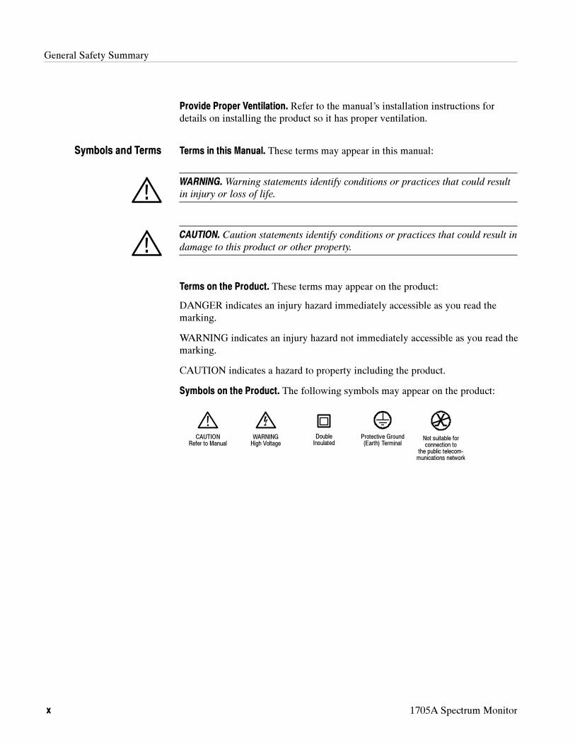
Provide Proper Ventilation. Refer to the manual’s installation instructions fordetails on installing the product so it has proper ventilation.
Terms in this Manual. These terms may appear in this manual:
WARNING.Warning statements identify conditions or practices that could result
in injury or loss of life.
CAUTION. Caution statements identify conditions or practices that could result in
damage to this product or other property.
Terms on the Product. These terms may appear on the product:
DANGER indicates an injury hazard immediately accessible as you read themarking.
WARNING indicates an injury hazard not immediately accessible as you read themarking.
CAUTION indicates a hazard to property including the product.
Symbols on the Product. The following symbols may appear on the product:
CAUTIONRefer to Manual
WARNINGHigh Voltage
DoubleInsulated
Protective Ground(Earth) Terminal
Not suitable forconnection to
the public telecom-munications network
Symbols and Terms

1705A Spectrum Monitor xi
Service Safety Summary
Only qualified personnel should perform service procedures. Read this ServiceSafety Summary and the General Safety Summary before performing any serviceprocedures.
Do Not Service Alone. Do not perform internal service or adjustments of thisproduct unless another person capable of rendering first aid and resuscitation ispresent.
Disconnect Power. To avoid electric shock, switch off the instrument power, thendisconnect the power cord from the mains power.
Use Caution When Servicing the CRT. To avoid electric shock or injury, useextreme caution when handling the CRT. Only qualified personnel familiar withCRT servicing procedures and precautions should remove or install the CRT.
CRTs retain hazardous voltages for long periods of time after power is turned off.Before attempting any servicing, discharge the CRT by shorting the anode tochassis ground. When discharging the CRT, connect the discharge path to groundand then the anode. Rough handling may cause the CRT to implode. Do not nickor scratch the glass or subject it to undue pressure when removing or installing it.When handling the CRT, wear safety goggles and heavy gloves for protection.
Use Care When Servicing With Power On. Dangerous voltages or currents mayexist in this product. Disconnect power, remove battery (if applicable), anddisconnect test leads before removing protective panels, soldering, or replacingcomponents.
To avoid electric shock, do not touch exposed connections.
X-Radiation. To avoid x-radiation exposure, do not modify or otherwise alter thehigh-voltage circuitry or the CRT enclosure. X-ray emissions generated withinthis product have been sufficiently shielded.

Service Safety Summary
xii 1705A Spectrum Monitor
1705A Spectrum Monitor xiii
Preface
The information in this manual is intended for instrument operators and servicetechnicians. Operators are assumed to befamiliar with basic television terms andmeasurements. Qualified service technicians are also assumed to be familiar withtelevision terms and measurements, and have moderate experience with analogand logic circuits.
The manual is divided into two parts: Operator’s Information and ServiceInformation. The Operator’s Information is useful to both operators and servicetechnicians. The Service Information is intended only for qualified servicetechnicians.
Section 1, Introduction, includes a general description of the instrument followedby the Specifications. The Specifications include references to the correspond-ing Performance check steps.
Section 2, Operating Instructions, familiarizes the user with the front-- andrear--panel controls, connectors, and indicators; includes an operator’s check-outprocedure; and includes other operator familiarization information.
Section 3, Installation, includes electrical and mechanical installation informa-tion. The electrical installation information includes adjustments and operationalchanges available with the instrument. The mechanical installation informationincludes rackmounting, custom installation, and portable use.
Section 4, Theory of Operation, provides an over-all block diagram description and
detailed circuit descriptions. Read the block diagram description for an overview of the
instrument. The detailed circuit descriptions should be used with the block diagram and
schematic diagrams in the foldout pages for specific information about individual
circuits.
Section 5, Checks and Adjustments, includes the Performance Check Procedure and the
Adjustment Procedure. The Performance Check Procedure is used to verify that the
instrument’s performance is within its specifications, and the Adjustment Procedure is
used to adjust the instrument to meet its specifications. The procedures are preceded by
a list of recommended test equipment. Each procedure has a short form listing of the
individual steps.
Section 6, Maintenance, includes preventive, troubleshooting, and correctiveinformation.
Section 1, Introduction
Section 2, OperatingInstructions
Section 3, Installation
Section 4, Theory ofOperation
Section 5, Checks andAdjustments
Section 6, Maintenance
Preface
xiv 1705A Spectrum Monitor
Section 7, Options, documents instrument options. The information in thissection summarizes the options. Additional details are included in appro-priateplaces throughout the manual.
Section 8, Replaceable Electrical Parts, includes order information and partnumbers for all replaceable electrical parts.
Section 9, Diagrams, contains servicing illustra-tions. These include adjustmentlocations, circuit board part locations, a block diagram, and schematic diagrams.Parts locating tables are included that cross--reference the circuit board illustra-tions to the schematic diagrams.
Section 10, Replaceable Mechanical Parts, includes ordering information andpart numbers for all replaceable mechanical parts. This parts list is referenced toan exploded view mechanical drawing. Also included are lists of accessories andoptional accessories.
Section 7, Options
Section 8, ReplaceableElectrical Parts
Section 9, Diagrams
Section 10, ReplaceableMechanical Parts
Preface
1705A Spectrum Monitor xv
Contacting Tektronix
Phone 1-800-833-9200*
Address Tektronix, Inc.Department or name (if known)14200 SW Karl Braun DriveP.O. Box 500Beaverton, OR 97077USA
Web site www.tektronix.com
Sales support 1-800-833-9200, select option 1*
Service support 1-800-833-9200, select option 2*
Technical support Email: [email protected]
1-800-833-9200, select option 3*
6:00 a.m. -- 5:00 p.m. Pacific time
* This phone number is toll free in North America. After office hours, please leave avoice mail message.Outside North America, contact a Tektronix sales office or distributor; see theTektronix web site for a list of offices.

Preface
xvi 1705A Spectrum Monitor

Introduction

1705A Spectrum Monitor 1- 1
Section 1Introduction
The TEKTRONIX 1705A Spectrum Monitor is an 8½” wide by 5¼” highspecial purpose spectrum analyzer. It weighs approximately 8½ pounds and ispowered from an ac source. The crt occupies approximately two-thirds of thefront-panel area, with the control panel taking up the remainder of the space.Operation is controlled by a microprocessor that polls the front-panel switches.Front-panel switches are of the momentary touch type with lighted functionalindicators. In addition to polling the front panel, the microprocessor providesthe characters for an alphanumeric crt readout.
The signal is displayed on a bright crt. It is of the mesh type, for bettergeometry, and uses an internal graticule to reduce parallax. Variable graticulescale illumination provides even lighting over the usable graticule area toimprove measurement accuracy and the quality of display photographs.
The 1705A Spectrum Monitor is a swept front-end superheterodyne-typespectrum analyzer with two inputs; L--Band to accommodate Low-NoiseAmplifier/Block Down Converter (LNB) outputs, and 70 MHz for use withVideo Exciters. The L--Band input (950 to 1800 MHz) is through an F-typeconnector, while the 70 MHz input is through a standard bnc connector. TheL--BAND INPUT connector is the output for the selectable 18 V supply that isthe Block Down Converter auxiliary power.
Typical Configurations
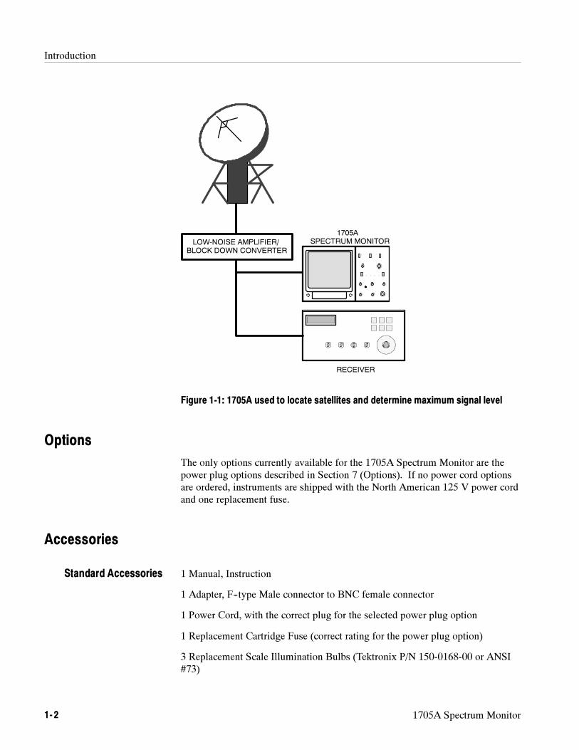
The TEKTRONIX 1705A Spectrum Monitor is designed primarily for use inlocating satellites and monitoring their signals. It is designed so that it can berack mounted, in a dual-width rack adapter, along with a half-rack waveformmonitor, such as a TEKTRONIX 1740-Series Waveform/Vector Monitor.However, it can be used as a portable instrument. It is intended to be connectedto the rf feed with a directional connector. See Figure 1-1. It is capable ofproviding the dc power required to run an LNB. The auxiliary LNB power isturned on or off by a rear-panel slide switch. An indicator on the rear panellights when the +18 V supply is operating normally.
Introduction
1- 2 1705A Spectrum Monitor
LOW-NOISE AMPLIFIER/BLOCK DOWN CONVERTER
1705ASPECTRUM MONITOR
RECEIVER
Figure 1-1: 1705A used to locate satellites and determine maximum signal level
Options
The only options currently available for the 1705A Spectrum Monitor are thepower plug options described in Section 7 (Options). If no power cord optionsare ordered, instruments are shipped with the North American 125 V power cordand one replacement fuse.
Accessories
1 Manual, Instruction
1 Adapter, F--type Male connector to BNC female connector
1 Power Cord, with the correct plug for the selected power plug option
1 Replacement Cartridge Fuse (correct rating for the power plug option)
3 Replacement Scale Illumination Bulbs (Tektronix P/N 150-0168-00 or ANSI#73)
Standard Accessories
Introduction
1705A Spectrum Monitor 1- 3
Camera, C9 (Option 20)
Viewing Hood (016-0475-00)
Front Panel Cover (200-3897-01)
1700F00, Plain Cabinet (painted silver grey)
1700F02, Portable Cabinet (painted silver grey with handle, feet, and frontcover)
1700F05, Side-by-Side Rack Adapter
1700F06, Blank Half-Rack Width Panel
1700F07, Utility Drawer
Safety Information
The 1705A Spectrum Monitor is intended to operate from an ac power sourcethat will not apply more than 250 V rms between the supply conductors orbetween either supply conductor and ground. A protective ground connection,by way of the grounding conductor, is essential for safe operation.
The instrument was tested for compliance in a cabinet. To ensure continuedcompliance, the instrument will need to be enclosed in a cabinet that is equiva-lent to those listed as Optional Accessories for the 1705A. A drawing of the1700F00 plain cabinet is contained in the Installation Instructions (Section 3).
Optional Accessories
Introduction
1- 4 1705A Spectrum Monitor
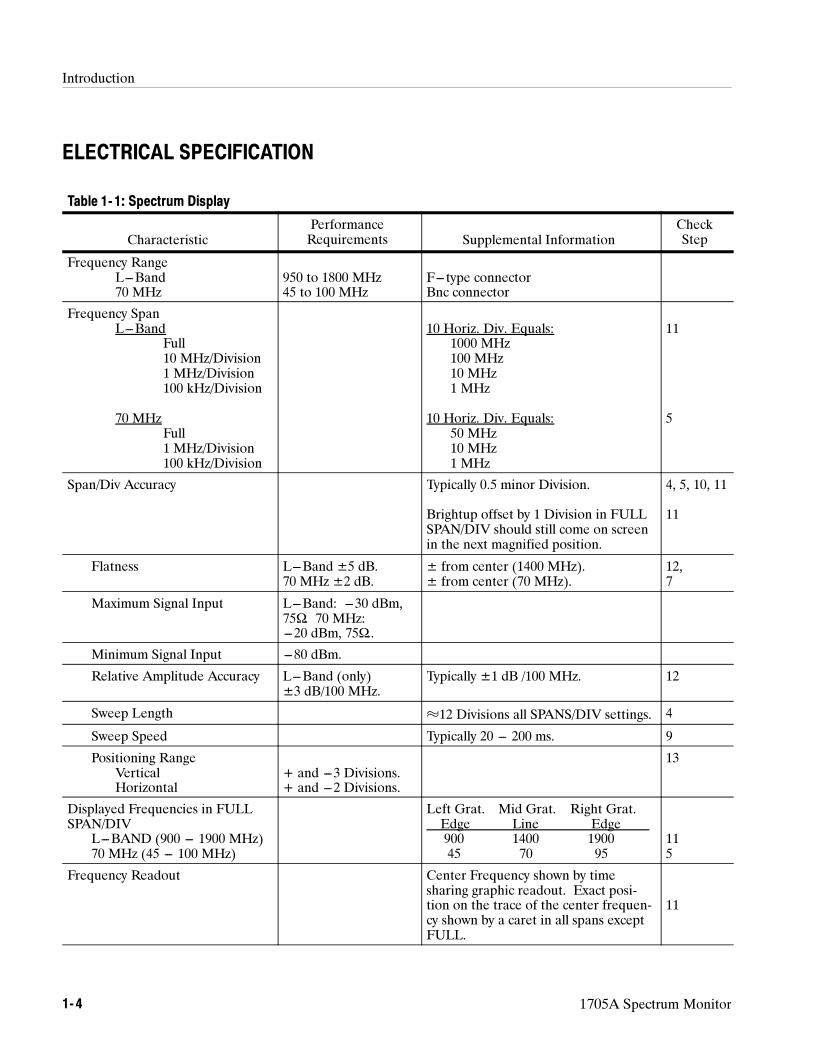
ELECTRICAL SPECIFICATION
Table 1- 1: Spectrum Display
CharacteristicPerformanceRequirements Supplemental Information
CheckStep
Frequency RangeL---Band70 MHz
950 to 1800 MHz45 to 100 MHz
F---type connectorBnc connector
Frequency SpanL---Band
Full10 MHz/Division1 MHz/Division100 kHz/Division
70 MHzFull1 MHz/Division100 kHz/Division
10 Horiz. Div. Equals:1000 MHz100 MHz10 MHz1 MHz
10 Horiz. Div. Equals:50 MHz10 MHz1 MHz
11
5
Span/Div Accuracy Typically 0.5 minor Division.
Brightup offset by 1 Division in FULLSPAN/DIV should still come on screenin the next magnified position.
4, 5, 10, 11
11
Flatness L---Band ±5 dB.70 MHz ±2 dB.
± from center (1400 MHz).± from center (70 MHz).
12,7
Maximum Signal Input L---Band: ---30 dBm,75Ω. 70 MHz:---20 dBm, 75Ω..
Minimum Signal Input ---80 dBm.
Relative Amplitude Accuracy L---Band (only)±3 dB/100 MHz.
Typically ±1 dB /100 MHz. 12
Sweep Length ¶12 Divisions all SPANS/DIV settings. 4
Sweep Speed Typically 20 --- 200 ms. 9
Positioning RangeVerticalHorizontal
+ and ---3 Divisions.+ and ---2 Divisions.
13
Displayed Frequencies in FULLSPAN/DIV
L---BAND (900 --- 1900 MHz)70 MHz (45 --- 100 MHz)
Left Grat. Mid Grat. Right Grat.Edge Line Edge900 1400 190045 70 95
115
Frequency Readout Center Frequency shown by timesharing graphic readout. Exact posi-tion on the trace of the center frequen-cy shown by a caret in all spans exceptFULL.
11
Introduction
1705A Spectrum Monitor 1- 5
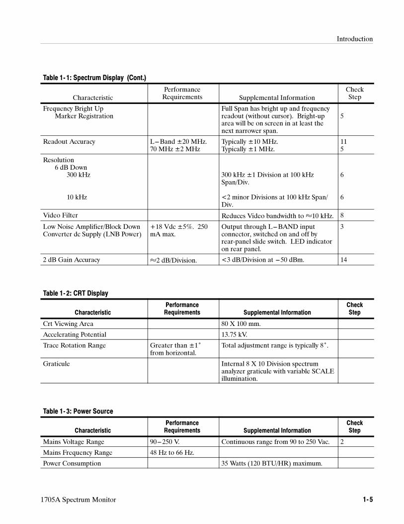
Table 1- 1: Spectrum Display (Cont.)
CharacteristicCheckStepSupplemental Information
PerformanceRequirements
Frequency Bright UpMarker Registration
Full Span has bright up and frequencyreadout (without cursor). Bright-uparea will be on screen in at least thenext narrower span.
5
Readout Accuracy L---Band ±20 MHz.70 MHz ±2 MHz
Typically ±10 MHz.Typically ±1 MHz.
115
Resolution6 dB Down
300 kHz
10 kHz
300 kHz ±1 Division at 100 kHzSpan/Div.
<2 minor Divisions at 100 kHz Span/Div.
6
6
Video Filter Reduces Video bandwidth to ¶10 kHz. 8
Low Noise Amplifier/Block DownConverter dc Supply (LNB Power)
+18 Vdc ±5%. 250mA max.
Output through L---BAND inputconnector, switched on and off byrear-panel slide switch. LED indicatoron rear panel.
3
2 dB Gain Accuracy ¶2 dB/Division. <3 dB/Division at ---50 dBm. 14
Table 1- 2: CRT Display
CharacteristicPerformanceRequirements Supplemental Information
CheckStep
Crt Viewing Area 80 X 100 mm.
Accelerating Potential 13.75 kV.
Trace Rotation Range Greater than ±1˚from horizontal.
Total adjustment range is typically 8˚.
Graticule Internal 8 X 10 Division spectrumanalyzer graticule with variable SCALEillumination.
Table 1- 3: Power Source
CharacteristicPerformanceRequirements Supplemental Information
CheckStep
Mains Voltage Range 90---250 V. Continuous range from 90 to 250 Vac. 2
Mains Frequency Range 48 Hz to 66 Hz.
Power Consumption 35 Watts (120 BTU/HR) maximum.
Introduction
1- 6 1705A Spectrum Monitor
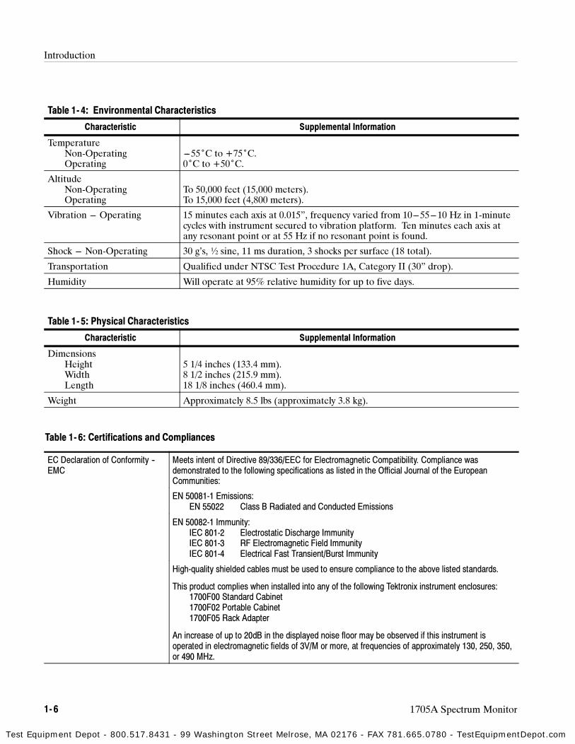
Table 1- 4: Environmental Characteristics
Characteristic Supplemental Information
TemperatureNon-OperatingOperating
---55˚C to +75˚C.0˚C to +50˚C.
AltitudeNon-OperatingOperating
To 50,000 feet (15,000 meters).To 15,000 feet (4,800 meters).
Vibration --- Operating 15 minutes each axis at 0.015”, frequency varied from 10---55---10 Hz in 1-minutecycles with instrument secured to vibration platform. Ten minutes each axis atany resonant point or at 55 Hz if no resonant point is found.
Shock --- Non-Operating 30 g’s, ½ sine, 11 ms duration, 3 shocks per surface (18 total).
Transportation Qualified under NTSC Test Procedure 1A, Category II (30” drop).
Humidity Will operate at 95% relative humidity for up to five days.
Table 1- 5: Physical Characteristics
Characteristic Supplemental Information
DimensionsHeightWidthLength
5 1/4 inches (133.4 mm).8 1/2 inches (215.9 mm).18 1/8 inches (460.4 mm).
Weight Approximately 8.5 lbs (approximately 3.8 kg).
Table 1- 6: Certifications and Compliances
EC Declaration of Conformity --EMC
Meets intent of Directive 89/336/EEC for Electromagnetic Compatibility. Compliance wasdemonstrated to the following specifications as listed in the Official Journal of the EuropeanCommunities:
EN 50081-1 Emissions:EN 55022 Class B Radiated and Conducted Emissions
EN 50082-1 Immunity:IEC 801-2 Electrostatic Discharge ImmunityIEC 801-3 RF Electromagnetic Field ImmunityIEC 801-4 Electrical Fast Transient/Burst Immunity
High-quality shielded cables must be used to ensure compliance to the above listed standards.
This product complies when installed into any of the following Tektronix instrument enclosures:1700F00 Standard Cabinet1700F02 Portable Cabinet1700F05 Rack Adapter
An increase of up to 20dB in the displayed noise floor may be observed if this instrument isoperated in electromagnetic fields of 3V/M or more, at frequencies of approximately 130, 250, 350,or 490 MHz.
Test Equipment Depot - 800.517.8431 - 99 Washington Street Melrose, MA 02176 - FAX 781.665.0780 - TestEquipmentDepot.com
Introduction
1705A Spectrum Monitor 1- 7
Table 1- 6: Certifications and Compliances (cont.)
FCC Compliance Emissions comply with FCC Code of Federal Regulations 47, Part 15, Subpart B, Class A Limits
Installation (Overvoltage)Category
Terminals on this product may have different installation (overvoltage) category designations. Theinstallation categories are:
CAT III Distribution-level mains (usually permanently connected). Equipment at this level istypically in a fixed industrial location.
CAT II Local-level mains (wall sockets). Equipment at this level includes appliances, portabletools, and similar products. Equipment is usually cord-connected.
CAT I Secondary (signal level) or battery operated circuits of electronic equipment.
Pollution Degree A measure of the contaminates that could occur in the environment around and within a product.Typically the internal environment inside a product is considered to be the same as the external.Products should be used only in the environment for which they are rated.
Pollution Degree 1 No pollution or only dry, nonconductive pollution occurs. Products inthis category are generally encapsulated, hermetically sealed, orlocated in clean rooms.
Pollution Degree 2 Normally only dry, nonconductive pollution occurs. Occasionally atemporary conductivity that is caused by condensation must beexpected. This location is a typical office/home environment.Temporary condensation occurs only when the product is out ofservice.
Pollution Degree 3 Conductive pollution, or dry, nonconductive pollution that becomesconductive due to condensation. These are sheltered locations whereneither temperature nor humidity is controlled. The area is protectedfrom direct sunshine, rain, or direct wind.
Pollution Degree 4 Pollution that generates persistent conductivity through conductivedust, rain, or snow. Typical outdoor locations.
Safety Standards
U.S. Nationally RecognizedTesting Laboratory Listing
UL1244 Standard for electrical and electronic measuring and test equipment.
Canadian Certification CAN/CSA C22.2 No. 231 CSA safety requirements for electrical and electronic measuring andtest equipment.
European Union Compliance Low Voltage Directive 73/23/EEC, amended by 93/69/EEC
EN 61010-1 Safety requirements for electrical equipment for measurement,control, and laboratory use.
Additional Compliance IEC61010-1 Safety requirements for electrical equipment for measurement,control, and laboratory use.
Introduction
1- 8 1705A Spectrum Monitor
Table 1- 6: Certifications and Compliances (cont.)
Safety Certification Compliance
Temperature, operating +5 to +40 C
Altitude (maximum operating) 2000 meters
Equipment Type Test and measuring
Safety Class Class 1 (as defined in IEC 1010-1, Annex H) -- grounded product
Overvoltage Category Overvoltage Category II (as defined in IEC 1010-1, Annex J)
Pollution Degree Pollution Degree 2 (as defined in IEC 1010-1). Note: Rated for indoor use only.
Introduction
1705A Spectrum Monitor 1- 9
APPLICATIONS
The principal application for the TEKTRONIX 1705A Spectrum Monitor is toprovide a convenient method to locate and identify Ku-Band satellites, find thecorrect transponder and check on its availability, and optimize antenna position-ing and polarization. The remainder of this section provides basic satellitecommunications application data. Specific operating instructions are located inSection 2, Operating Instructions.
The communications satellites that the television industry is interested in lie in aband directly over the earth’s equator, at a distance of approximately 35,900 km(or about 3.7 times the earth’s diameter). Traveling at approximately11,000 km/h the satellite completes one full orbit in 23 hours, 56 minutes,4.9 seconds, which is referred to as a sidereal day. When a satellite completesone orbit in a sidereal day it is geographically stationary (geostationary) to apoint on the earth’s surface. Without being geostationary, using a satellite wouldbe extremely complicated and the calculations required to determine when theywere in the usable window, and how long they would stay there would, in mostcases, require a computer.
At 35,900 km distance the earth subtends an angle of 18˚, which providescoverage of approximately 40% of the earth’s surface. See Figure 1-2. Fortypercent (40%) of the earth’s surface corresponds to an area stretching from 70˚North latitude to 70˚ South latitude. For rough assumptions, a satellite, ingeostationary orbit over the equator, could cover latitudes from the Arctic circle(66˚ 30’ N) to the Antarctic circle (66˚ 30’ S). However it should be noted thateven though the satellite is capable of covering 40% of the earth’s surface theactual coverage will be less in most cases because of the antenna design andavailable transmitter power.
9,675 km35,900 km
18°
70° N
70° S
Figure 1-2: Relationship of a communications satellite to earth
Determining the exact angle from the horizon to a satellite (other than at theequator) requires a knowledge of trigonometry, because of the relatively close
Locating Satellites
Introduction
1- 10 1705A Spectrum Monitor
orbit of the satellite. If the orbit of an equatorial orbiting satellite were roughlyequal to the distance from earth to the sun, ordinary latitude could be used todetermine the elevation of the antenna, which is, of necessity, very finelyfocused. However since there is a disparity this angle is somewhat less than thelatitude for the earth station. See Figure 1-3. Simple logic readily points outthat as the latitude increases the angle from horizon to the satellite decreases. Anexample of this would be that at 45˚ North or South latitude the angle above thehorizon is about 40˚ for a satellite at the earth station’s longitude. Figure 1-3illustrates why it is not possible to pinpoint a satellite with ordinary navigation.
A
EARTH
SATELLITE
SUN
00°(EQUATOR)
45° N
Figure 1-3: Angle A (the difference at a specific latitude between the angle to thesun and the angle to a satellite) is the reason ordinary navigation techniquescannot be used to find a satellite
Figure 1-4 confirms that the angle from the prime meridian to a satellite will beconsiderably different than the angle from a North American or European earthstation to the same satellite. It should also be noted that the elevation alsodecreases for a satellite the further east or west from the earth station’s longitude.
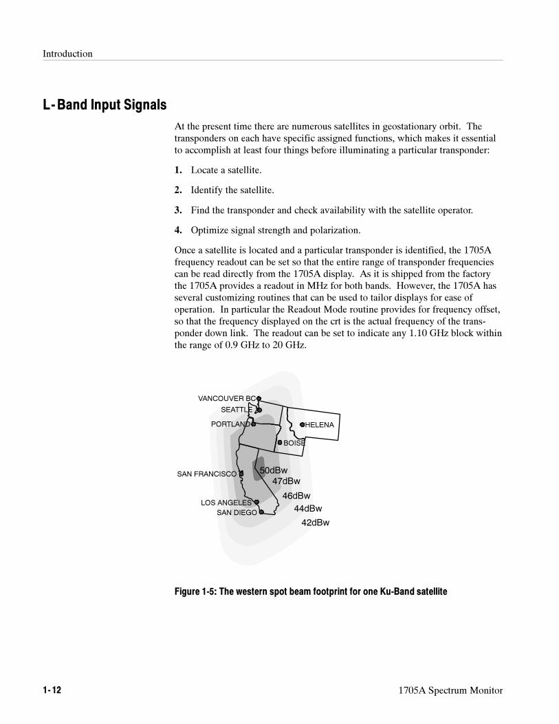
Even though a satellite, in theory, can communicate with 40% of the earth’ssurface from its location, in most cases it will not. The antenna systems onboardthe satellites are usually designed to cover a specific area. These areas arereferred to as hemispheres, zones, and spots. A hemispherical beam is designedto cover roughly 40% of the earth’s surface, for example, the western hemi-sphere. A zonal beam covers a specific area, for example, the ContinentalUnited States, which is usually referred to as the CONUS beam. A spot beam isexactly what it implies, concentrating on a smaller geographical area, such as thewestern United States. With each of these beams there are areas where the signalstrength is greater. Figure 1-5 shows a propagation map for the western spotbeam for one Ku--Band satellite.
Satellite Footprints
Introduction
1705A Spectrum Monitor 1- 11
NEW YORK CITY CHICAGOLOS ANGELES
HONOLULU
ANCHORAGE
GREENWICH
ENGLAND
NORTH
POLE
PRIME MERIDIAN
000°
INTERNATIONAL DATELINE
180°
45°W
45°E
90°E
135°E
135°W
SPACENET 2
69°
RCA K2
81°
RCA K1
85°
SBS 3
97°
GSTAR A2
103° GSTAR A1
105° ANIK B
109°
ANIK C2
112.5°
SPACENET 1
120°
MORELOS 1
113.5°
MORELOS 2
116.5°
SBS 5
122°
ASC 1
128°
ARCTIC
CIRCLE
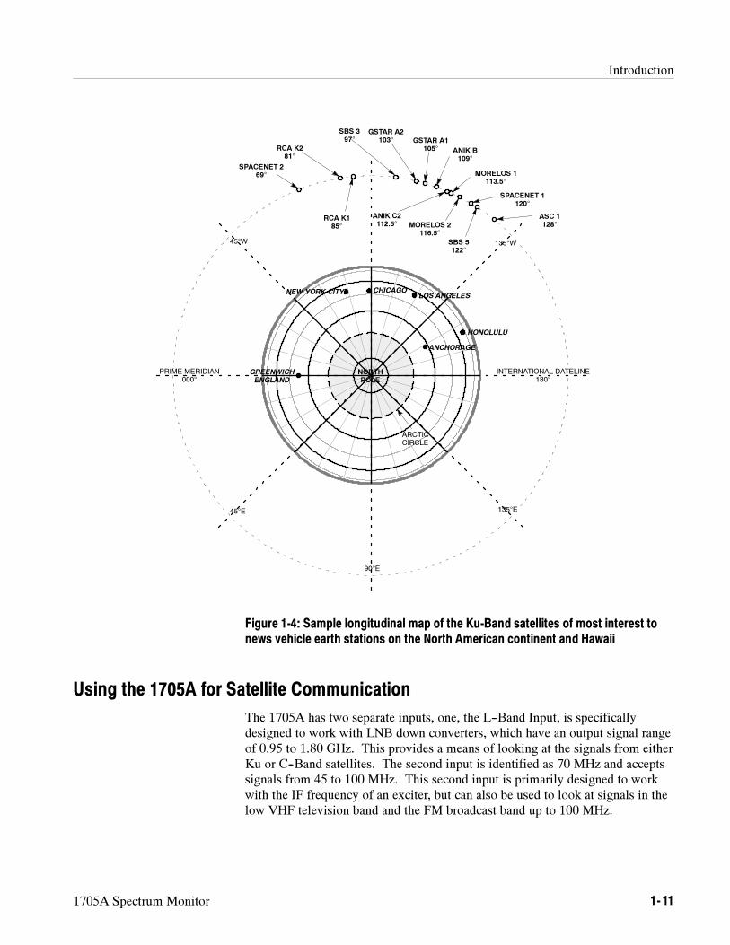
Figure 1-4: Sample longitudinal map of the Ku-Band satellites of most interest tonews vehicle earth stations on the North American continent and Hawaii
Using the 1705A for Satellite Communication
The 1705A has two separate inputs, one, the L--Band Input, is specificallydesigned to work with LNB down converters, which have an output signal rangeof 0.95 to 1.80 GHz. This provides a means of looking at the signals from eitherKu or C--Band satellites. The second input is identified as 70 MHz and acceptssignals from 45 to 100 MHz. This second input is primarily designed to workwith the IF frequency of an exciter, but can also be used to look at signals in thelow VHF television band and the FM broadcast band up to 100 MHz.
Introduction
1- 12 1705A Spectrum Monitor
L-Band Input Signals
At the present time there are numerous satellites in geostationary orbit. Thetransponders on each have specific assigned functions, which makes it essentialto accomplish at least four things before illuminating a particular transponder:
1. Locate a satellite.
2. Identify the satellite.
3. Find the transponder and check availability with the satellite operator.
4. Optimize signal strength and polarization.
Once a satellite is located and a particular transponder is identified, the 1705Afrequency readout can be set so that the entire range of transponder frequenciescan be read directly from the 1705A display. As it is shipped from the factorythe 1705A provides a readout in MHz for both bands. However, the 1705A hasseveral customizing routines that can be used to tailor displays for ease ofoperation. In particular the Readout Mode routine provides for frequency offset,so that the frequency displayed on the crt is the actual frequency of the trans-ponder down link. The readout can be set to indicate any 1.10 GHz block withinthe range of 0.9 GHz to 20 GHz.
HELENA
BOISE
VANCOUVER BC
SEATTLE
PORTLAND
SAN FRANCISCO
LOS ANGELES
SAN DIEGO
50dBw
47dBw
46dBw
44dBw
42dBw
Figure 1-5: The western spot beam footprint for one Ku-Band satellite
Introduction
1705A Spectrum Monitor 1- 13
Zeroing in on a Satellite
In almost all cases a set procedure for Locating, Identifying, Finding (transpond-ers), and Optimizing will be followed. The 1705A Spectrum Monitor is a toolthat greatly simplifies the individual steps so the correct satellite transponder canbe accessed in the minimum time.
In most cases the elevation (angle above the horizon) and the true azimuth(direction east or west to the satellite) of the antenna will be the same as it wasfor the previous access of the same satellite. This angle can be found in one oftwo ways, calculation or approximation from previous accesses; however, nomatter how the satellite is located the signal path will need to be optimized. Inmost cases the approximate location of the satellite is known from previoustransactions and only identification of transponders and signal strength remain tobe dealt with.
Each of the satellites has one or more singular characteristics. In many cases thesingular characteristics can be easily identified on the spectrum monitor, whichcan save valuable setup time. These characteristics can take the form oftelemetry beacons, transponder polarization schemes, or blocks of non-videosignals that stand out. And in a few cases, the easiest method of identificationmay be the fact that the satellite is near another satellite that is readily identifi-able.
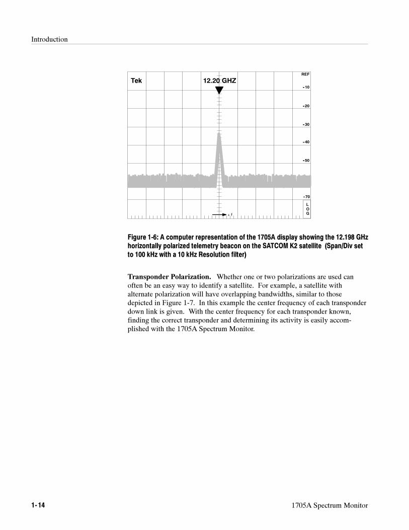
Telemetry Beacons. Satellites have special tracking or telemetry beacons thatare easily recognizable on the spectrum monitor. Not only do these assist inidentifying the satellite, but they provide an accurate way to set the frequencyoffset to correspond with actual satellite frequencies. Figure 1-6 shows a typicalKu--Band satellite telemetry beacon. Note that the 1705A readout frequency canbe offset to read the down link frequency in GHz. Similar beacons can be foundon some C--Band satellites also.
Locating the Satellite
Identifying the Satellite
Introduction
1- 14 1705A Spectrum Monitor
Tek
REF
--10
--20
--30
--40
--50
--60
--70
L
O
G+ f
12.20 GHZ
Figure 1-6: A computer representation of the 1705A display showing the 12.198 GHzhorizontally polarized telemetry beacon on the SATCOM K2 satellite (Span/Div setto 100 kHz with a 10 kHz Resolution filter)
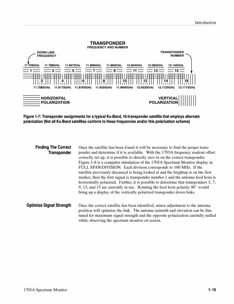
Transponder Polarization. Whether one or two polarizations are used canoften be an easy way to identify a satellite. For example, a satellite withalternate polarization will have overlapping bandwidths, similar to thosedepicted in Figure 1-7. In this example the center frequency of each transponderdown link is given. With the center frequency for each transponder known,finding the correct transponder and determining its activity is easily accom-plished with the 1705A Spectrum Monitor.
Introduction
1705A Spectrum Monitor 1- 15
11.729GHz 11.788GHz 11.847GHz 11.906GHz 11.965GHz 12.024GHz 12.083GHz 12.142GHz
11.7585GHz 11.8175GHz 11.8765GHz 11.9355GHz 11.9945GHz 12.0535GHz 12.1125GHz 12.1715GHz
1
2
3
4
5
6
7
8
9
10
11
12
13
14
15
16
HORIZONTAL
POLARIZATION
VERTICAL
POLARIZATION
DOWN LINK
FREQUENCY
TRANSPONDER
NUMBER
FREQUENCY AND NUMBER
TRANSPONDER
Figure 1-7: Transponder assignments for a typical Ku-Band, 16-transponder satellite that employs alternatepolarization (Not all Ku-Band satellites conform to these frequencies and/or this polarization scheme)
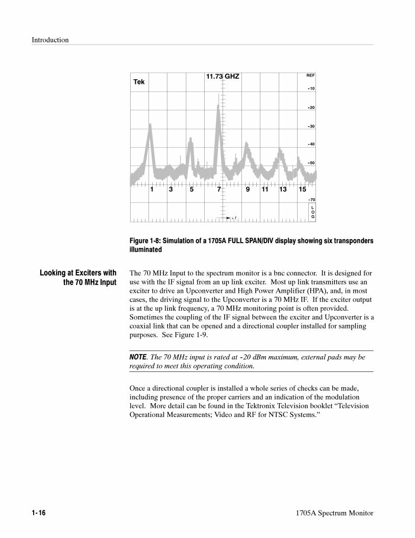
Once the satellite has been found it will be necessary to find the proper trans-ponder and determine if it is available. With the 1705A frequency readout offsetcorrectly set up, it is possible to directly zero in on the correct transponder.Figure 1-8 is a computer simulation of the 1705A Spectrum Monitor display inFULL SPAN/DIVISION. Each division corresponds to 100 MHz. If thesatellite previously discussed is being looked at and the brightup is on the firstmarker, then the first signal is transponder number 1 and the antenna feed horn ishorizontally polarized. Further, it is possible to determine that transponders 5, 7,9, 13, and 15 are currently in use. Rotating the feed horn polarity 90˚ wouldbring up a display of the vertically polarized transponder down links.
Once the correct satellite has been identified, minor adjustment to the antennaposition will optimize the link. The antenna azimuth and elevation can be finetuned for maximum signal strength and the opposite polarization carefully nulledwhile observing the spectrum monitor crt screen.
Finding The CorrectTransponder
Optimize Signal Strength
Introduction
1- 16 1705A Spectrum Monitor
Tek
REF
--10
--20
--30
--40
--50
--60
--70
L
O
G+ f
11.73 GHZ
1 3 5 7 9 11 13 15
Figure 1-8: Simulation of a 1705A FULL SPAN/DIV display showing six transpondersilluminated
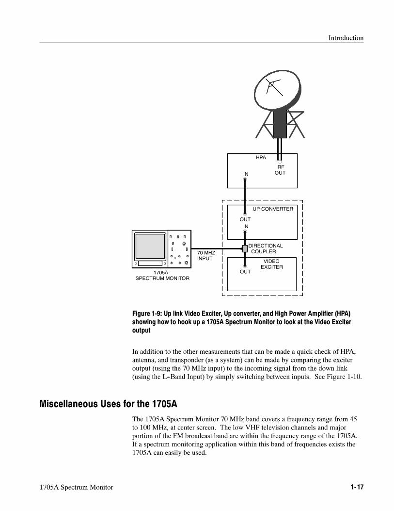
The 70 MHz Input to the spectrum monitor is a bnc connector. It is designed foruse with the IF signal from an up link exciter. Most up link transmitters use anexciter to drive an Upconverter and High Power Amplifier (HPA), and, in mostcases, the driving signal to the Upconverter is a 70 MHz IF. If the exciter outputis at the up link frequency, a 70 MHz monitoring point is often provided.Sometimes the coupling of the IF signal between the exciter and Upconverter is acoaxial link that can be opened and a directional coupler installed for samplingpurposes. See Figure 1-9.
NOTE. The 70 MHz input is rated at --20 dBm maximum, external pads may be
required to meet this operating condition.
Once a directional coupler is installed a whole series of checks can be made,including presence of the proper carriers and an indication of the modulationlevel. More detail can be found in the Tektronix Television booklet “TelevisionOperational Measurements; Video and RF for NTSC Systems.”
Looking at Exciters withthe 70 MHz Input
Introduction
1705A Spectrum Monitor 1- 17
1705ASPECTRUM MONITOR
IN
RFOUT
HPA
OUT
IN
UP CONVERTER
OUT
VIDEOEXCITER
70 MHZINPUT
DIRECTIONALCOUPLER
Figure 1-9: Up link Video Exciter, Up converter, and High Power Amplifier (HPA)showing how to hook up a 1705A Spectrum Monitor to look at the Video Exciteroutput
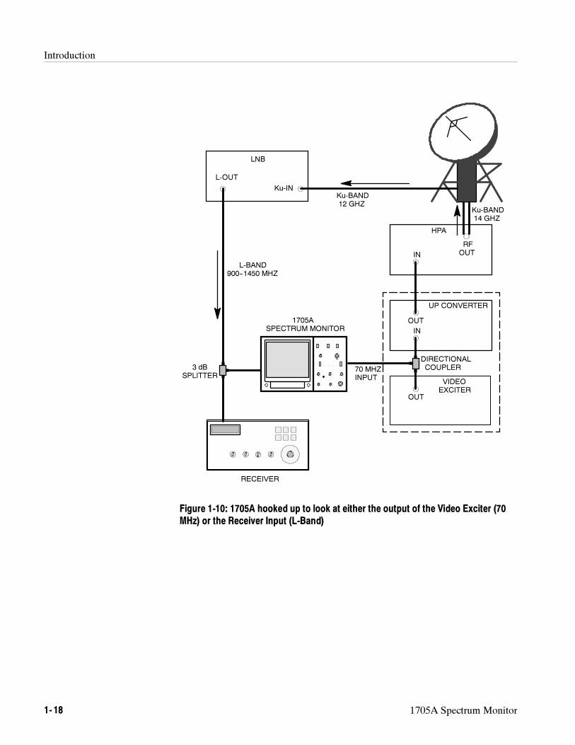
In addition to the other measurements that can be made a quick check of HPA,antenna, and transponder (as a system) can be made by comparing the exciteroutput (using the 70 MHz input) to the incoming signal from the down link(using the L--Band Input) by simply switching between inputs. See Figure 1-10.
Miscellaneous Uses for the 1705A
The 1705A Spectrum Monitor 70 MHz band covers a frequency range from 45to 100 MHz, at center screen. The low VHF television channels and majorportion of the FM broadcast band are within the frequency range of the 1705A.If a spectrum monitoring application within this band of frequencies exists the1705A can easily be used.
Introduction
1- 18 1705A Spectrum Monitor
1705ASPECTRUM MONITOR
IN
RFOUT
HPA
OUT
IN
UP CONVERTER
OUT
VIDEOEXCITER
70 MHZINPUT
DIRECTIONALCOUPLER
RECEIVER
LNB
L-OUT
Ku-IN
Ku-BAND14 GHZ
Ku-BAND12 GHZ
3 dBSPLITTER
L-BAND900--1450 MHZ
Figure 1-10: 1705A hooked up to look at either the output of the Video Exciter (70MHz) or the Receiver Input (L-Band)

Operating Instructions

1705A Spectrum Monitor 2- 1
Section 2Operating Instructions
These instructions provide information about the front-panel controls andindicators, rear-panel connectors and switch, powering-up, and the measurementgraticule and alphanumeric readout.
Front-panel Controls and Indicators
The front--panel controls and indicators consist of momentary contact push-but-ton switches, with backlit switch selections, and variable controls. For front-panel control and indicator locations, see Figure 2-1. There are also functionsthat are accessed by holding the switch down for approximately 1 second. Thesefunctions are identified by a blue box surrounding the front--panel label.
1. VIDEO
Turns on or off the Video Filter, which reduces the post detection bandwidth(video), to reduce the high-frequency components for display noiseaveraging. A front-panel LED indicator lights when the Video Filter is on.Holding the Video switch activates the High Gain mode. An on-screenreadout indicates 2 dB/Div. To exit this mode, hold the switch again, and theon-screen readout returns to 10 dB/Div. Gain selection will not affect themomentary touch VIDEO On/Off selection.
2. RESOLUTION
Selects the 2nd IF bandwidth. Toggles between 10 kHz and 300 kHz asindicated by the front-panel indicator.
3. INPUT
L--BAND or 70 MHz —A push-button switch to select either the L--BAND(900 to 2000 MHz) or the 70 MHz (45 to 100 MHz) input for display.Indicator lights show which input is displayed.
FILTER
INPUT
Operating Instructions
2- 2 1705A Spectrum Monitor
TektronixINPUT
DISPLAY
1705A
VIDEO
ON
SPECTRUM
MONITOR
POSITION
= HOLD FOR FUNCTION
FOCUS SCALE INTENS
ON 300 KHz
10 KHz
LBAND
70 MHz
POWER
1 2 34 56
78 91011 12 13
HORIZONTAL VERTICAL
RESOLUTION
FILTER
SWEEPSPEED
CENTER FREQUENCY
TRACEROTATION
100KHz
1
MHz MHz10 FULL
MENU
SPAN/DIV
TekREF
--10
--20
--30
--40
--50
--60
--70
L
O
G+ f
Figure 2-1: 1705A front panel; refer to text for descriptions of controls identified with circled numbers
4. SWEEP SPEED
A variable control that sets the sweep repetition rate, which is typicallybetween 20 and 200 ms.
5. CENTER FREQUENCY
A ten-turn variable control that determines the center frequency of thedisplayed portion of the spectrum.
SWEEP
Operating Instructions
1705A Spectrum Monitor 2- 3
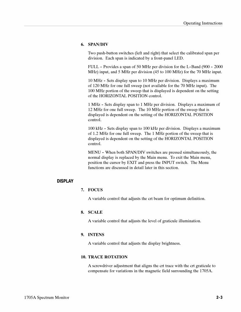
6. SPAN/DIV
Two push-button switches (left and right) that select the calibrated span perdivision. Each span is indicated by a front-panel LED.
FULL -- Provides a span of 50 MHz per division for the L--Band (900 -- 2000MHz) input, and 5 MHz per division (45 to 100 MHz) for the 70 MHz input.
10 MHz -- Sets display span to 10 MHz per division. Displays a maximumof 120 MHz for one full sweep (not available for the 70 MHz input). The100 MHz portion of the sweep that is displayed is dependent on the settingof the HORIZONTAL POSITION control.
1 MHz -- Sets display span to 1 MHz per division. Displays a maximum of12 MHz for one full sweep. The 10 MHz portion of the sweep that isdisplayed is dependent on the setting of the HORIZONTAL POSITIONcontrol.
100 kHz -- Sets display span to 100 kHz per division. Displays a maximumof 1.2 MHz for one full sweep. The 1 MHz portion of the sweep that isdisplayed is dependent on the setting of the HORIZONTAL POSITIONcontrol.
MENU -- When both SPAN/DIV switches are pressed simultaneously, thenormal display is replaced by the Main menu. To exit the Main menu,position the cursor by EXIT and press the INPUT switch. The Menufunctions are discussed in detail later in this section.
7. FOCUS
A variable control that adjusts the crt beam for optimum definition.
8. SCALE
A variable control that adjusts the level of graticule illumination.
9. INTENS
A variable control that adjusts the display brightness.
10. TRACE ROTATION
A screwdriver adjustment that aligns the crt trace with the crt graticule tocompensate for variations in the magnetic field surrounding the 1705A.
DISPLAY
Operating Instructions
2- 4 1705A Spectrum Monitor
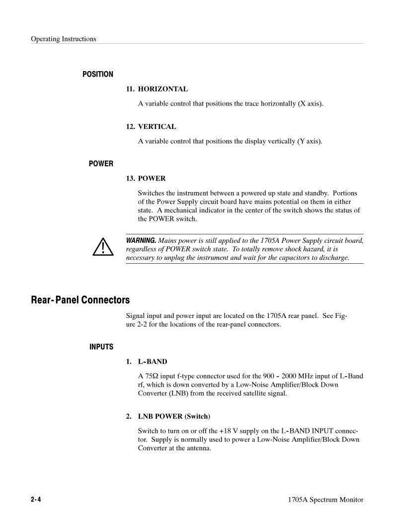
11. HORIZONTAL
A variable control that positions the trace horizontally (X axis).
12. VERTICAL
A variable control that positions the display vertically (Y axis).
13. POWER
Switches the instrument between a powered up state and standby. Portionsof the Power Supply circuit board have mains potential on them in eitherstate. A mechanical indicator in the center of the switch shows the status ofthe POWER switch.
WARNING.Mains power is still applied to the 1705A Power Supply circuit board,
regardless of POWER switch state. To totally remove shock hazard, it is
necessary to unplug the instrument and wait for the capacitors to discharge.
Rear-Panel Connectors
Signal input and power input are located on the 1705A rear panel. See Fig-ure 2-2 for the locations of the rear-panel connectors.
1. L--BAND
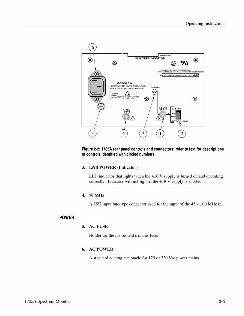
A 75Ω input f-type connector used for the 900 -- 2000 MHz input of L--Bandrf, which is down converted by a Low-Noise Amplifier/Block DownConverter (LNB) from the received satellite signal.
2. LNB POWER (Switch)
Switch to turn on or off the +18 V supply on the L--BAND INPUT connec-tor. Supply is normally used to power a Low-Noise Amplifier/Block DownConverter at the antenna.
POSITION
POWER
INPUTS
Operating Instructions
1705A Spectrum Monitor 2- 5
70 MHz
SPECTRUMMONITOR
333--3990--01
INPUT
BESCHLEUNIGUNGSSPANNUNG KLEINERALS20kV
DIE IN DIESEM GERATENTSTEHENDERONTGENSTRAHLUNG IST AUSREICHENDABGESCHIRMT
1 234
6
5
WARNINGTO AVOID ELECTRICAL SHOCK, THE POWERCORD PROTECTIVEGROUNDING CONDUCTORMUST BECONNECTEDTO EARTH GROUND.
0.7AMAX50/60Hz
90-250VREPLACE FUSEONLYWITH250V 2A F TYPE
L BANDINPUT
!
LNB POW-
ER
ON
!
LNB POW-
ER
OFF
+18 VDC@ 250 mA
ON
Figure 2-2: 1705A rear panel controls and connectors; refer to text for descriptionsof controls identified with circled numbers
3. LNB POWER (Indicator)
LED indicator that lights when the +18 V supply is turned on and operatingcorrectly. Indicator will not light if the +18 V supply is shorted.
4. 70 MHz
A 75Ω input bnc-type connector used for the input of the 45 -- 100 MHz rf.
5. AC FUSE
Holder for the instrument’s mains fuse.
6. AC POWER
A standard ac plug receptacle for 120 or 220 Vac power mains.
POWER
Operating Instructions
2- 6 1705A Spectrum Monitor
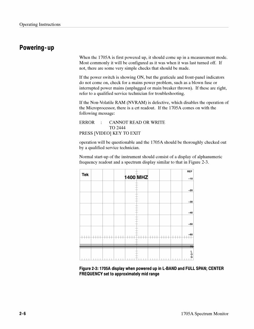
Powering-up
When the 1705A is first powered up, it should come up in a measurement mode.Most commonly it will be configured as it was when it was last turned off. Ifnot, there are some very simple checks that should be made.
If the power switch is showing ON, but the graticule and front-panel indicatorsdo not come on, check for a mains power problem, such as a blown fuse orinterrupted power mains (unplugged or main breaker thrown). If these are right,refer to a qualified service technician for troubleshooting.
If the Non-Volatile RAM (NVRAM) is defective, which disables the operation ofthe Microprocessor, there is a crt readout. If the 1705A comes on with thefollowing message:
ERROR : CANNOT READ OR WRITETO 2444
PRESS [VIDEO] KEY TO EXIT
operation will be questionable and the 1705A should be thoroughly checked outby a qualified service technician.
Normal start-up of the instrument should consist of a display of alphanumericfrequency readout and a spectrum display similar to that in Figure 2-3.
TekREF
--10
--20
--30
--40
--50
--60
--70
L
O
G
1400 MHZ
Figure 2-3: 1705A display when powered up in L-BAND and FULL SPAN; CENTERFREQUENCY set to approximately mid range
Operating Instructions
1705A Spectrum Monitor 2- 7
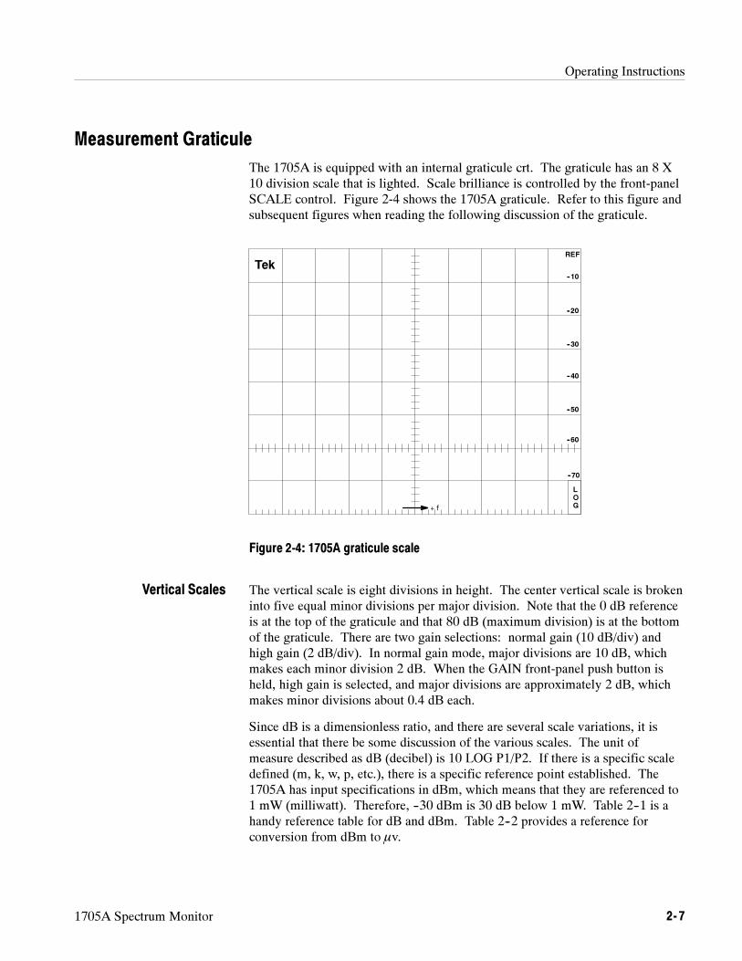
Measurement Graticule
The 1705A is equipped with an internal graticule crt. The graticule has an 8 X10 division scale that is lighted. Scale brilliance is controlled by the front-panelSCALE control. Figure 2-4 shows the 1705A graticule. Refer to this figure andsubsequent figures when reading the following discussion of the graticule.
Tek
REF
--10
--20
--30
--40
--50
--60
--70
L
O
G+ f
Figure 2-4: 1705A graticule scale
The vertical scale is eight divisions in height. The center vertical scale is brokeninto five equal minor divisions per major division. Note that the 0 dB referenceis at the top of the graticule and that 80 dB (maximum division) is at the bottomof the graticule. There are two gain selections: normal gain (10 dB/div) andhigh gain (2 dB/div). In normal gain mode, major divisions are 10 dB, whichmakes each minor division 2 dB. When the GAIN front-panel push button isheld, high gain is selected, and major divisions are approximately 2 dB, whichmakes minor divisions about 0.4 dB each.
Since dB is a dimensionless ratio, and there are several scale variations, it isessential that there be some discussion of the various scales. The unit ofmeasure described as dB (decibel) is 10 LOG P1/P2. If there is a specific scaledefined (m, k, w, p, etc.), there is a specific reference point established. The1705A has input specifications in dBm, which means that they are referenced to1 mW (milliwatt). Therefore, --30 dBm is 30 dB below 1 mW. Table 2--1 is ahandy reference table for dB and dBm. Table 2--2 provides a reference forconversion from dBm to v.
Vertical Scales
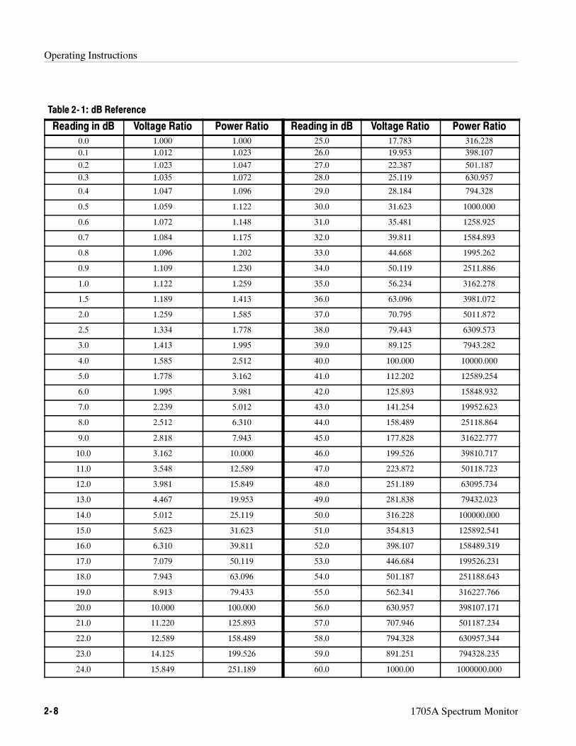
Operating Instructions
2- 8 1705A Spectrum Monitor
Table 2- 1: dB Reference
Reading in dB Voltage Ratio Power Ratio Reading in dB Voltage Ratio Power Ratio
0.0 1.000 1.000 25.0 17.783 316.228
0.1 1.012 1.023 26.0 19.953 398.107
0.2 1.023 1.047 27.0 22.387 501.187
0.3 1.035 1.072 28.0 25.119 630.957
0.4 1.047 1.096 29.0 28.184 794.328
0.5 1.059 1.122 30.0 31.623 1000.000
0.6 1.072 1.148 31.0 35.481 1258.925
0.7 1.084 1.175 32.0 39.811 1584.893
0.8 1.096 1.202 33.0 44.668 1995.262
0.9 1.109 1.230 34.0 50.119 2511.886
1.0 1.122 1.259 35.0 56.234 3162.278
1.5 1.189 1.413 36.0 63.096 3981.072
2.0 1.259 1.585 37.0 70.795 5011.872
2.5 1.334 1.778 38.0 79.443 6309.573
3.0 1.413 1.995 39.0 89.125 7943.282
4.0 1.585 2.512 40.0 100.000 10000.000
5.0 1.778 3.162 41.0 112.202 12589.254
6.0 1.995 3.981 42.0 125.893 15848.932
7.0 2.239 5.012 43.0 141.254 19952.623
8.0 2.512 6.310 44.0 158.489 25118.864
9.0 2.818 7.943 45.0 177.828 31622.777
10.0 3.162 10.000 46.0 199.526 39810.717
11.0 3.548 12.589 47.0 223.872 50118.723
12.0 3.981 15.849 48.0 251.189 63095.734
13.0 4.467 19.953 49.0 281.838 79432.023
14.0 5.012 25.119 50.0 316.228 100000.000
15.0 5.623 31.623 51.0 354.813 125892.541
16.0 6.310 39.811 52.0 398.107 158489.319
17.0 7.079 50.119 53.0 446.684 199526.231
18.0 7.943 63.096 54.0 501.187 251188.643
19.0 8.913 79.433 55.0 562.341 316227.766
20.0 10.000 100.000 56.0 630.957 398107.171
21.0 11.220 125.893 57.0 707.946 501187.234
22.0 12.589 158.489 58.0 794.328 630957.344
23.0 14.125 199.526 59.0 891.251 794328.235
24.0 15.849 251.189 60.0 1000.00 1000000.000
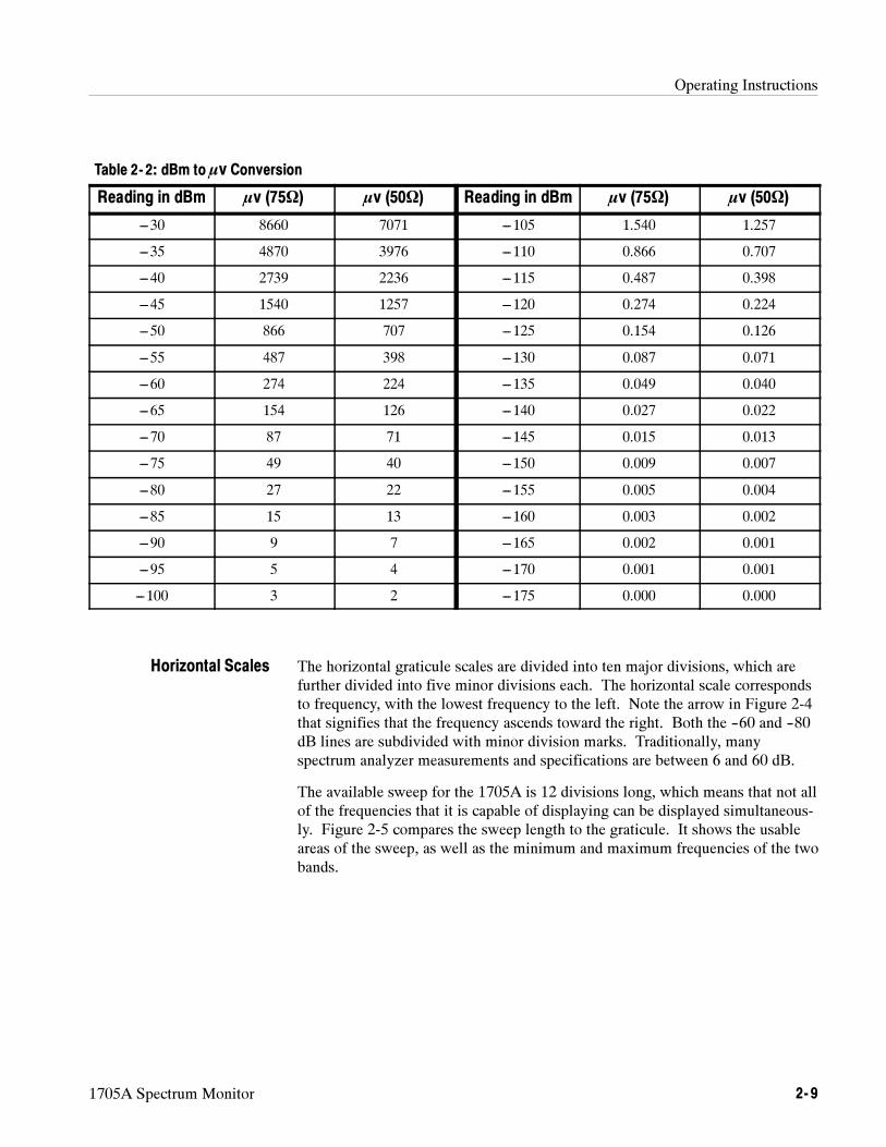
Operating Instructions
1705A Spectrum Monitor 2- 9
Table 2- 2: dBm to v Conversion
Reading in dBm v (75Ω) v (50Ω) Reading in dBm v (75Ω) v (50Ω)
---30 8660 7071 ---105 1.540 1.257
---35 4870 3976 ---110 0.866 0.707
---40 2739 2236 ---115 0.487 0.398
---45 1540 1257 ---120 0.274 0.224
---50 866 707 ---125 0.154 0.126
---55 487 398 ---130 0.087 0.071
---60 274 224 ---135 0.049 0.040
---65 154 126 ---140 0.027 0.022
---70 87 71 ---145 0.015 0.013
---75 49 40 ---150 0.009 0.007
---80 27 22 ---155 0.005 0.004
---85 15 13 ---160 0.003 0.002
---90 9 7 ---165 0.002 0.001
---95 5 4 ---170 0.001 0.001
---100 3 2 ---175 0.000 0.000
The horizontal graticule scales are divided into ten major divisions, which arefurther divided into five minor divisions each. The horizontal scale correspondsto frequency, with the lowest frequency to the left. Note the arrow in Figure 2-4that signifies that the frequency ascends toward the right. Both the --60 and --80dB lines are subdivided with minor division marks. Traditionally, manyspectrum analyzer measurements and specifications are between 6 and 60 dB.
The available sweep for the 1705A is 12 divisions long, which means that not allof the frequencies that it is capable of displaying can be displayed simultaneous-ly. Figure 2-5 compares the sweep length to the graticule. It shows the usableareas of the sweep, as well as the minimum and maximum frequencies of the twobands.
Horizontal Scales
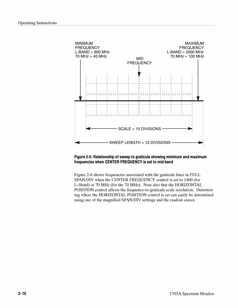
Operating Instructions
2- 10 1705A Spectrum Monitor
SCALE = 10 DIVISIONS
SWEEP LENGTH = 12 DIVISIONS
MINIMUM
FREQUENCY
L-BAND = 900 MHz
70 MHz = 45 MHzMID
FREQUENCY
MAXIMUM
FREQUENCY
L-BAND = 2000 MHz
70 MHz = 100 MHz
Figure 2-5: Relationship of sweep to graticule showing minimum and maximumfrequencies when CENTER FREQUENCY is set to mid band
Figure 2-6 shows frequencies associated with the graticule lines in FULLSPAN/DIV when the CENTER FREQUENCY control is set to 1400 (forL--Band) or 70 MHz (for the 70 MHz). Note also that the HORIZONTALPOSITION control affects the frequency-to-graticule scale resolution. Determin-ing where the HORIZONTAL POSITION control is set can easily be determinedusing one of the magnified SPAN/DIV settings and the readout cursor.
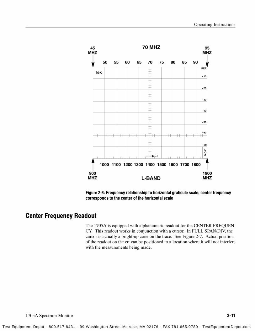
Operating Instructions
1705A Spectrum Monitor 2- 11
Tek
REF
--10
--20
--30
--40
--50
--60
--70
L
O
G+ f
45
MHZ
95
MHZ
1900
MHZ
900
MHZ
50 55 60 65 70 75 80 85 90
1000 1100 1200 1300 1400 1500 1600 1700 1800
70 MHZ
L-BAND
Figure 2-6: Frequency relationship to horizontal graticule scale; center frequencycorresponds to the center of the horizontal scale
Center Frequency Readout
The 1705A is equipped with alphanumeric readout for the CENTER FREQUEN-CY. This readout works in conjunction with a cursor. In FULL SPAN/DIV, thecursor is actually a bright-up zone on the trace. See Figure 2-7. Actual positionof the readout on the crt can be positioned to a location where it will not interferewith the measurements being made.
Test Equipment Depot - 800.517.8431 - 99 Washington Street Melrose, MA 02176 - FAX 781.665.0780 - TestEquipmentDepot.com
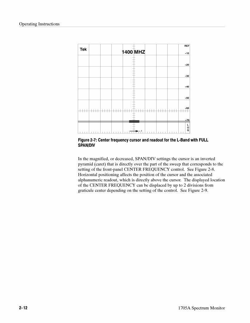
Operating Instructions
2- 12 1705A Spectrum Monitor
1400 MHZTek
REF
--10
--20
--30
--40
--50
--60
--70
L
O
G+ f
Figure 2-7: Center frequency cursor and readout for the L-Band with FULLSPAN/DIV
In the magnified, or decreased, SPAN/DIV settings the cursor is an invertedpyramid (caret) that is directly over the part of the sweep that corresponds to thesetting of the front-panel CENTER FREQUENCY control. See Figure 2-8.Horizontal positioning affects the position of the cursor and the associatedalphanumeric readout, which is directly above the cursor. The displayed locationof the CENTER FREQUENCY can be displaced by up to 2 divisions fromgraticule center depending on the setting of the control. See Figure 2-9.
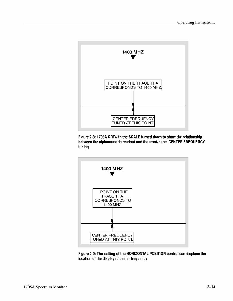
Operating Instructions
1705A Spectrum Monitor 2- 13
1400 MHZ
POINT ON THE TRACE THAT
CORRESPONDS TO 1400 MHZ.
CENTER FREQUENCY
TUNED AT THIS POINT.
Figure 2-8: 1705A CRTwith the SCALE turned down to show the relationshipbetween the alphanumeric readout and the front-panel CENTER FREQUENCYtuning
1400 MHZ
POINT ON THE
TRACE THAT
CORRESPONDS TO
1400 MHZ.
CENTER FREQUENCY
TUNED AT THIS POINT.
Figure 2-9: The setting of the HORIZONTAL POSITION control can displace thelocation of the displayed center frequency
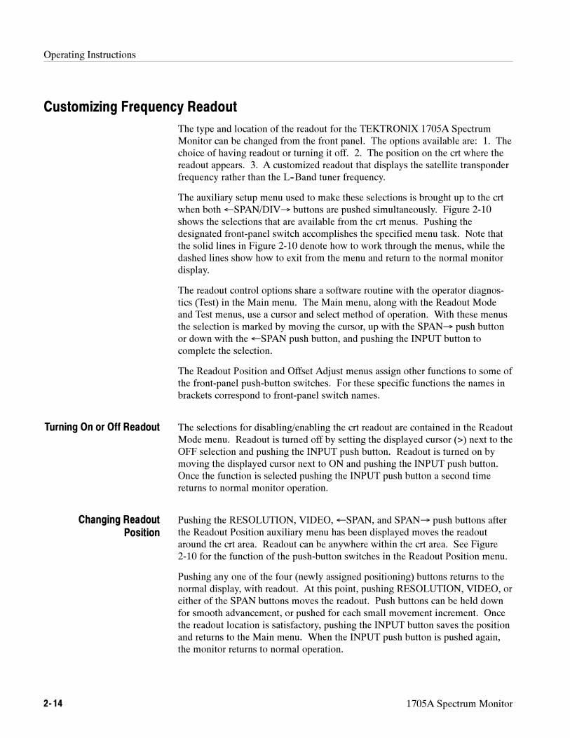
Operating Instructions
2- 14 1705A Spectrum Monitor
Customizing Frequency Readout
The type and location of the readout for the TEKTRONIX 1705A SpectrumMonitor can be changed from the front panel. The options available are: 1. Thechoice of having readout or turning it off. 2. The position on the crt where thereadout appears. 3. A customized readout that displays the satellite transponderfrequency rather than the L--Band tuner frequency.
The auxiliary setup menu used to make these selections is brought up to the crtwhen both ←SPAN/DIV→ buttons are pushed simultaneously. Figure 2-10shows the selections that are available from the crt menus. Pushing thedesignated front-panel switch accomplishes the specified menu task. Note thatthe solid lines in Figure 2-10 denote how to work through the menus, while thedashed lines show how to exit from the menu and return to the normal monitordisplay.
The readout control options share a software routine with the operator diagnos-tics (Test) in the Main menu. The Main menu, along with the Readout Modeand Test menus, use a cursor and select method of operation. With these menusthe selection is marked by moving the cursor, up with the SPAN→ push buttonor down with the←SPAN push button, and pushing the INPUT button tocomplete the selection.
The Readout Position and Offset Adjust menus assign other functions to some ofthe front-panel push-button switches. For these specific functions the names inbrackets correspond to front-panel switch names.
The selections for disabling/enabling the crt readout are contained in the ReadoutMode menu. Readout is turned off by setting the displayed cursor (>) next to theOFF selection and pushing the INPUT push button. Readout is turned on bymoving the displayed cursor next to ON and pushing the INPUT push button.Once the function is selected pushing the INPUT push button a second timereturns to normal monitor operation.
Pushing the RESOLUTION, VIDEO, ←SPAN, and SPAN→ push buttons afterthe Readout Position auxiliary menu has been displayed moves the readoutaround the crt area. Readout can be anywhere within the crt area. See Figure2-10 for the function of the push-button switches in the Readout Position menu.
Pushing any one of the four (newly assigned positioning) buttons returns to thenormal display, with readout. At this point, pushing RESOLUTION, VIDEO, oreither of the SPAN buttons moves the readout. Push buttons can be held downfor smooth advancement, or pushed for each small movement increment. Oncethe readout location is satisfactory, pushing the INPUT button saves the positionand returns to the Main menu. When the INPUT push button is pushed again,the monitor returns to normal operation.
Turning On or Off Readout
Changing ReadoutPosition
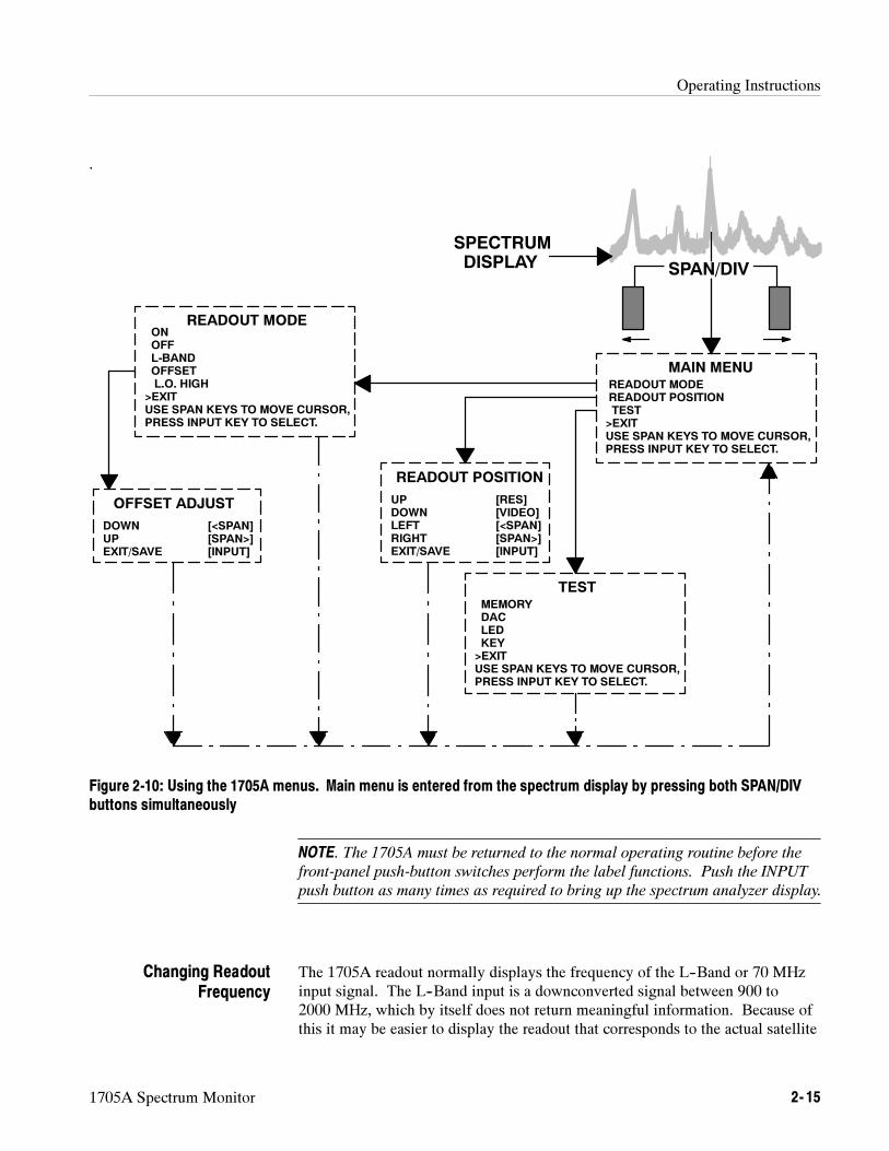
Operating Instructions
1705A Spectrum Monitor 2- 15
.
SPECTRUM
DISPLAY
READOUT MODEONOFFL-BANDOFFSETL.O. HIGH
>EXITUSE SPAN KEYS TO MOVE CURSOR,PRESS INPUT KEY TO SELECT.
MAIN MENU
READOUT MODEREADOUT POSITIONTEST
>EXITUSE SPAN KEYS TO MOVE CURSOR,PRESS INPUT KEY TO SELECT.
READOUT POSITION
OFFSET ADJUST
TEST
MEMORYDACLEDKEY
>EXITUSE SPAN KEYS TO MOVE CURSOR,PRESS INPUT KEY TO SELECT.
DOWNUPEXIT/SAVE
[<SPAN][SPAN>][INPUT]
UPDOWNLEFTRIGHTEXIT/SAVE
[RES][VIDEO][<SPAN][SPAN>][INPUT]
SPAN/DIV
Figure 2-10: Using the 1705A menus. Main menu is entered from the spectrum display by pressing both SPAN/DIVbuttons simultaneously
NOTE. The 1705A must be returned to the normal operating routine before the
front-panel push-button switches perform the label functions. Push the INPUT
push button as many times as required to bring up the spectrum analyzer display.
The 1705A readout normally displays the frequency of the L--Band or 70 MHzinput signal. The L--Band input is a downconverted signal between 900 to2000 MHz, which by itself does not return meaningful information. Because ofthis it may be easier to display the readout that corresponds to the actual satellite
Changing ReadoutFrequency
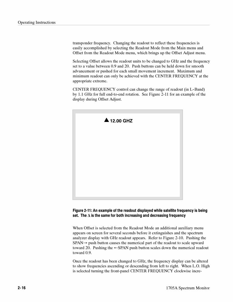
Operating Instructions
2- 16 1705A Spectrum Monitor
transponder frequency. Changing the readout to reflect these frequencies iseasily accomplished by selecting the Readout Mode from the Main menu andOffset from the Readout Mode menu, which brings up the Offset Adjust menu.
Selecting Offset allows the readout units to be changed to GHz and the frequencyset to a value between 0.9 and 20. Push buttons can be held down for smoothadvancement or pushed for each small movement increment. Maximum andminimum readout can only be achieved with the CENTER FREQUENCY at theappropriate extreme.
CENTER FREQUENCY control can change the range of readout (in L--Band)by 1.1 GHz for full end-to-end rotation. See Figure 2-11 for an example of thedisplay during Offset Adjust.
12.00 GHZ
Figure 2-11: An example of the readout displayed while satellite frequency is beingset. The ∆ is the same for both increasing and decreasing frequency
When Offset is selected from the Readout Mode an additional auxiliary menuappears on screen for several seconds before it extinguishes and the spectrumanalyzer display with GHz readout appears. Refer to Figure 2-10. Pushing theSPAN→ push button causes the numerical part of the readout to scale upwardtoward 20. Pushing the←SPAN push button scales down the numerical readouttoward 0.9.
Once the readout has been changed to GHz, the frequency display can be alteredto show frequencies ascending or descending from left to right. When L.O. Highis selected turning the front-panel CENTER FREQUENCY clockwise incre-
Operating Instructions
1705A Spectrum Monitor 2- 17
ments the frequency readout (low to high) and moves the brightened portion ofthe sweep from left to right. When L.O. Low is selected the readout decrements(high to low) and the brightened portion of the sweep moves from left to right,with clockwise rotation of the CENTER FREQUENCY.
When L--Band is selected from the Readout Mode menu, the Main menu returnsand the readout is scaled in MHz. Changes of frequency readout are shown inascending order when the front-panel CENTER FREQUENCY control is rotatedclockwise.
Once the satellite frequency and L.O. have been set, pushing the INPUT pushbutton saves the display and returns the Main menu. Pushing the INPUT pushbutton again returns to normal monitor operation.
NOTE. The 1705A must be returned to the normal operating routine before the
front-panel push-button switches perform the label functions. Push the INPUT
push-button as many times as required to bring up the spectrum analyzer
display.
The series of tests that can be made are documented in Section 6, Maintenance,under the sub-section heading of “General Troubleshooting Techniques.”
Locating Ku-Band Satellites
The TEKTRONIX 1705A Spectrum Monitor is specifically designed to help thetelevision news vehicle operator quickly and properly address a satellite. Eventhough the 1705A will be most often used for Ku--Band transmissions, it can beused with any satellite system that can be downconverted to its L--Band inputfrequencies.
The following operating procedure is typical and can be adjusted to fit particularvehicle and operator preferences.
1. The expected true azimuth and elevation to the satellite from a specificlocation should be determined by calculation or reference to Table 2--3 forpopular news satellites. Table 2--3 lists 21 Continental United States(CONUS) cities; the cities in the table are spotted around the country andcan help to approximate (the location of a satellite) from any area of the 48contiguous states.
Test Mode
Basic OperatingProcedure
Operating Instructions
2- 18 1705A Spectrum Monitor
2. Stabilize the vehicle in a location where there will be a clear path betweenthe antenna and the satellite. The vehicle should be reasonably level tofacilitate antenna and polarization adjustment.
3. Point the antenna in the expected direction of the satellite. Note thatcompass readings may not be accurate in the presence of vehicles orstructures. Several readings, at nearby locations, should be taken todetermine any unusual effects. Appropriate correction for magnetic variationmust be made when a magnetic compass is used. The locating tablesindicate true north.
4. If the antenna azimuth and elevation are remotely adjusted, the TEKTRO-NIX 1705A may be permanently connected to the splitter feeding theL--Band downlink signal from the outdoor Low Noise Block Converter(LNB) to the indoor receiver. If the antenna is to be adjusted manually, aportable ac or battery-powered 1705A may be connected directly to the LNBat the antenna, in which case the spectrum monitor can be used to power theLNB.
Table 2- 3: Azimuth / Elevation Table for 21 CONUS Cities
CITY
SATCOM K2 G--STAR II SBS--3
CITYAZ EL AZ EL AZ EL
Atlanta 175˚ 50˚ 214˚ 45˚ 199˚ 49˚
Boston 195˚ 40˚ 225˚ 31˚ 214˚ 36˚
Chicago 170˚ 41˚ 205˚ 38˚ 190˚ 41˚
Dallas /Ft. Worth 150˚ 47˚ 192˚ 53˚ 172˚ 51˚
Denver 145˚ 38˚ 180˚ 44˚ 165˚ 43˚
Detroit 177˚ 44˚ 212˚ 38˚ 198˚ 42˚
Houston 153˚ 52˚ 199˚ 53˚ 180˚ 55˚
Las Vegas 131˚ 35˚ 163˚ 47˚ 148˚ 43˚
Los Angeles 127˚ 34˚ 158˚ 48˚ 143˚ 43˚
Miami 180˚ 61˚ 227˚ 49˚ 211˚ 55˚
Minneapolis/St Paul 164˚ 37˚ 198˚ 37˚ 184˚ 38˚
Nashville 170˚ 48˚ 209˚ 44˚ 193˚ 47˚
New Orleans 162˚ 54˚ 208˚ 51˚ 190˚ 55˚
New York 191˚ 42˚ 223˚ 33˚ 211˚ 38˚
Philadelphia 189˚ 43˚ 222˚ 34˚ 210˚ 39˚
Phoenix 132˚ 39˚ 168˚ 51˚ 150˚ 47˚
Operating Instructions
1705A Spectrum Monitor 2- 19
Table 2- 3: Azimuth / Elevation Table for 21 CONUS Cities (Cont.)
Salt Lake City 137˚ 34˚ 169˚ 42˚ 155˚ 39˚
San Francisco 125˚ 28˚ 154˚ 42˚ 140˚ 38˚
Seattle 131˚ 22˚ 158˚ 32˚ 146˚ 29˚
St. Louis 166˚ 44˚ 204˚ 42˚ 188˚ 45˚
Washington DC 186˚ 45˚ 221˚ 36˚ 216˚ 38˚
5. If the antenna is pointed close to a satellite, one or both polarizations of thefull satellite will appear on the screen because the 1705A Spectrum Monitoris a much more sensitive indicator than a receiver and picture monitor.Initially, there is no need to be concerned with antenna polarization or whichsatellite channels may be active.
6. If no satellite signal is observed, or the incorrect satellite is identified, sweepthe antenna azimuth carefully around the expected satellite direction. If nosatellite is found, return the azimuth to the expected direction and increase(or decrease) the elevation by about one degree and resweep the azimuth.
7. When a satellite signal has been observed on the 1705A display, it may beidentified by the nature of the signals on the satellite. For example, widebandwidth NBC television signals with multiple audio and data carriers onmany transponders will identify Satcom K--2. Other satellites will havesimilar identifying characteristics. If the incorrect satellite has been selected,repoint the antenna to locate the desired satellite. Once any satellite is foundand identified, a reference point is established and nearby satellites may belocated by moving the antenna carefully in the proper direction.
8. Optimize the antenna by carefully adjusting azimuth and elevation whileobserving the signal strength on the 1705A Spectrum Monitor. At this timeone or both satellite polarizations will be observed, but the received signalmay not be a viewable picture for a picture monitor.
9. The polarization must be adjusted in a transmit/receive system by rotatingthe antenna feed to minimize the undesired, cross polarized signal.
WARNING. This adjustment requires a spectrum monitor and should not be
attempted using a receiver and picture monitor alone. Any mis-adjustment will
put the transmit signal on the wrong satellite transponder and create interfer-
ence with another user. Furthur access to the satellite may be denied!
As the antenna feed is rotated, observe that there will be a sharp null ofsignals on one polarization or the other. Rotate the feed carefully to null thesignals of the polarization that will not be used. Most news vehicle feed
Operating Instructions
2- 20 1705A Spectrum Monitor
systems are single polarization receive to avoid the possibility of nulling thewrong polarization. If the antenna is set up to receive more than onepolarization, be sure that the feed polarization being observed is associatedwith the transponder that will be used for the transmission.
10. Before transmitting, the satellite operator will need to be contacted. Theoperator will want a transmit signal to be brought up to verify correcttransponder, signal polarization, and to determine the correct operatingpower. If the antenna and transmitting system are correctly adjusted, thischeck will only take seconds. This check may be permitted earlier in theday, if time is available and the antenna or transmitter setting are not to bechanged.
11. During transmit, the 1705A may be used to verify the presence of video,audio, and any communications signals at the 70 MHz output of the VideoExciter. This signal may be permanently connected to the 1705A, along withthe L--Band receive connection, to allow front-panel selection. With eitherinput, narrower spans may be selected to permit observing discrete signals.
12. Be sure that there is an agreed upon “good night” for the transmission. Thecarrier will not be watching your program content, and must know clearlywhen you are finished with the satellite. Unless there is a specific agree-ment, the carrier will expect a telephone call to know you are clear, and youwill be charged.

The following servicing instructions are for use only by qualified personnel. Toavoid injury, do not perform any servicing other than that stated in the operating
instructions unless you are qualified to do so. Refer to all safety summaries beforeperforming any service.
WARNING


Installation

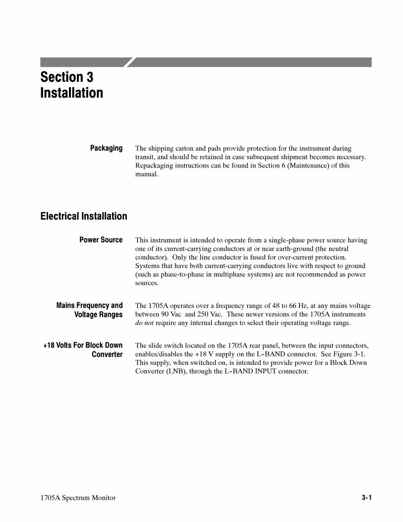
1705A Spectrum Monitor 3- 1
Section 3Installation
The shipping carton and pads provide protection for the instrument duringtransit, and should be retained in case subsequent shipment becomes necessary.Repackaging instructions can be found in Section 6 (Maintenance) of thismanual.
Electrical Installation
This instrument is intended to operate from a single-phase power source havingone of its current-carrying conductors at or near earth-ground (the neutralconductor). Only the line conductor is fused for over-current protection.Systems that have both current-carrying conductors live with respect to ground(such as phase-to-phase in multiphase systems) are not recommended as powersources.
The 1705A operates over a frequency range of 48 to 66 Hz, at any mains voltagebetween 90 Vac and 250 Vac. These newer versions of the 1705A instrumentsdo not require any internal changes to select their operating voltage range.
The slide switch located on the 1705A rear panel, between the input connectors,enables/disables the +18 V supply on the L--BAND connector. See Figure 3-1.This supply, when switched on, is intended to provide power for a Block DownConverter (LNB), through the L--BAND INPUT connector.
Packaging
Power Source
Mains Frequency andVoltage Ranges
+18 Volts For Block DownConverter
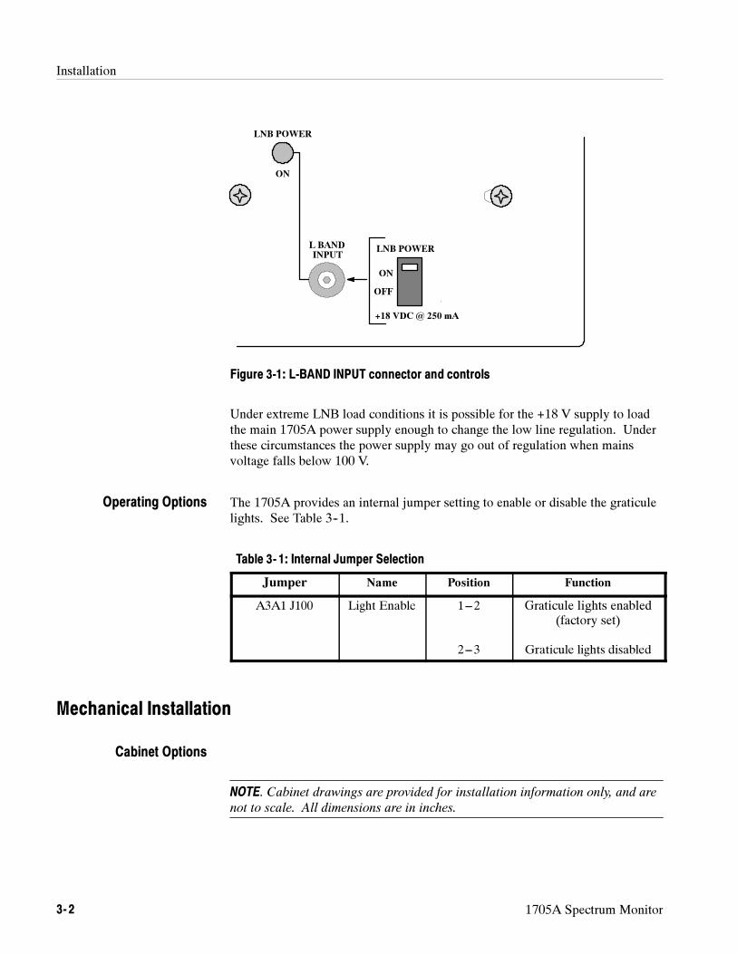
Installation
3- 2 1705A Spectrum Monitor
L BANDINPUT
LNB POWER
ON
LNB POWER
OFF
+18 VDC@ 250 mA
ON
Figure 3-1: L-BAND INPUT connector and controls
Under extreme LNB load conditions it is possible for the +18 V supply to loadthe main 1705A power supply enough to change the low line regulation. Underthese circumstances the power supply may go out of regulation when mainsvoltage falls below 100 V.
The 1705A provides an internal jumper setting to enable or disable the graticulelights. See Table 3--1.
Table 3- 1: Internal Jumper Selection
Jumper Name Position Function
A3A1 J100 Light Enable 1---2
2---3
Graticule lights enabled(factory set)
Graticule lights disabled
Mechanical Installation
NOTE. Cabinet drawings are provided for installation information only, and are
not to scale. All dimensions are in inches.
Operating Options
Cabinet Options
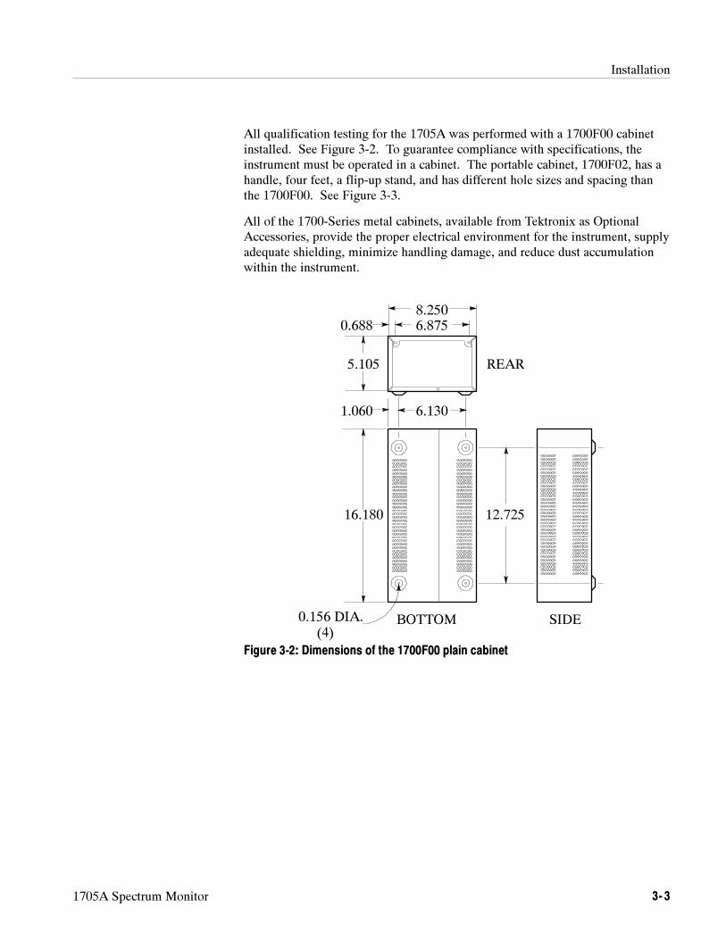
Installation
1705A Spectrum Monitor 3- 3
All qualification testing for the 1705A was performed with a 1700F00 cabinetinstalled. See Figure 3-2. To guarantee compliance with specifications, theinstrument must be operated in a cabinet. The portable cabinet, 1700F02, has ahandle, four feet, a flip-up stand, and has different hole sizes and spacing thanthe 1700F00. See Figure 3-3.
All of the 1700-Series metal cabinets, available from Tektronix as OptionalAccessories, provide the proper electrical environment for the instrument, supplyadequate shielding, minimize handling damage, and reduce dust accumulationwithin the instrument.
REAR
6.130
BOTTOM SIDE
12.725
8.2506.8750.688
1.060
16.180
5.105
0.156 DIA.(4)
Figure 3-2: Dimensions of the 1700F00 plain cabinet
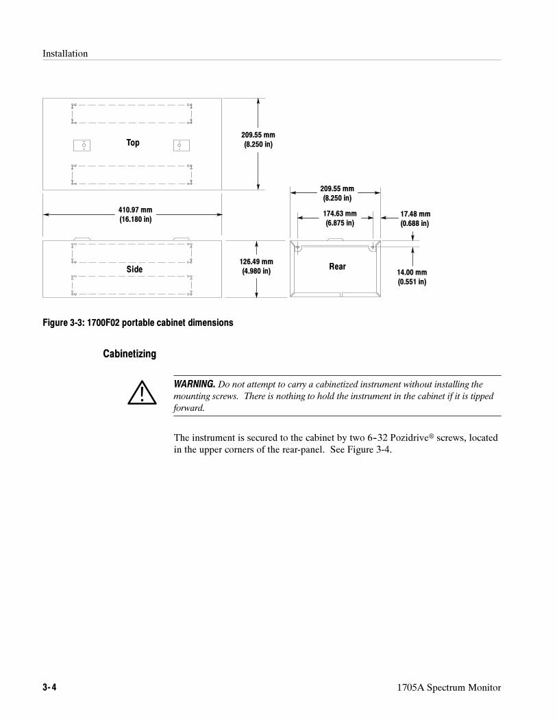
Installation
3- 4 1705A Spectrum Monitor
Top
410.97 mm(16.180 in)
126.49 mm(4.980 in)
Rear
209.55 mm(8.250 in)
174.63 mm(6.875 in)
17.48 mm(0.688 in)
14.00 mm(0.551 in)
Side
209.55 mm(8.250 in)
Figure 3-3: 1700F02 portable cabinet dimensions
WARNING. Do not attempt to carry a cabinetized instrument without installing the
mounting screws. There is nothing to hold the instrument in the cabinet if it is tipped
forward.
The instrument is secured to the cabinet by two 6--32 Pozidrive screws, locatedin the upper corners of the rear-panel. See Figure 3-4.
Cabinetizing
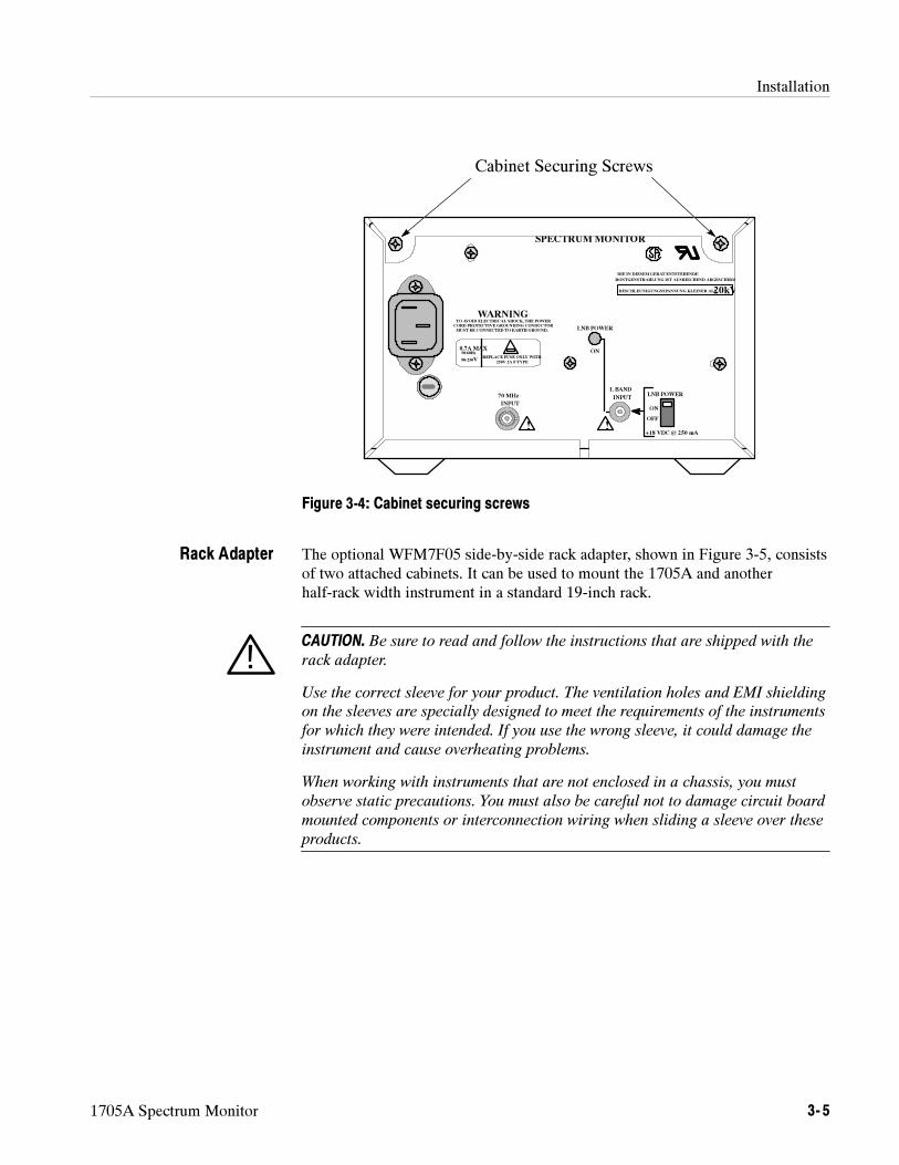
Installation
1705A Spectrum Monitor 3- 5
LNB POWER
70 MHz
SPECTRUMMONITOR
333--3990--01
INPUT
BESCHLEUNIGUNGSSPANNUNGKLEINER ALS20kV
DIE IN DIESEMGERAT ENTSTEHENDE
RONTGENSTRAHLUNG IST AUSREICHEND ABGESCHIRMT
WARNINGTOAVOID ELECTRICAL SHOCK, THE POWER
CORD PROTECTIVE GROUNDINGCONDUCTORMUST BE CONNECTED TOEARTHGROUND.
0.7AMAX50/60Hz
90-250VREPLACE FUSE ONLY WITH
250V 2A F TYPE
L BAND
INPUT
!
ON
!
LNB POWER
OFF
+18 VDC@ 250 mA
ON
Cabinet Securing Screws
Figure 3-4: Cabinet securing screws
The optional WFM7F05 side-by-side rack adapter, shown in Figure 3-5, consistsof two attached cabinets. It can be used to mount the 1705A and anotherhalf-rack width instrument in a standard 19-inch rack.
CAUTION. Be sure to read and follow the instructions that are shipped with the
rack adapter.
Use the correct sleeve for your product. The ventilation holes and EMI shielding
on the sleeves are specially designed to meet the requirements of the instruments
for which they were intended. If you use the wrong sleeve, it could damage the
instrument and cause overheating problems.
When working with instruments that are not enclosed in a chassis, you must
observe static precautions. You must also be careful not to damage circuit board
mounted components or interconnection wiring when sliding a sleeve over these
products.
Rack Adapter
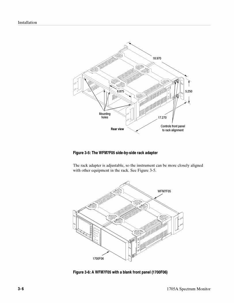
Installation
3- 6 1705A Spectrum Monitor
18.970
5.250
17.270
Controls front panelto rack alignmentRear view
6.875
Mountingholes
Figure 3-5: The WFM7F05 side-by-side rack adapter
The rack adapter is adjustable, so the instrument can be more closely alignedwith other equipment in the rack. See Figure 3-5.
WFM7F05
1700F06
Figure 3-6: A WFM7F05 with a blank front panel (1700F06)
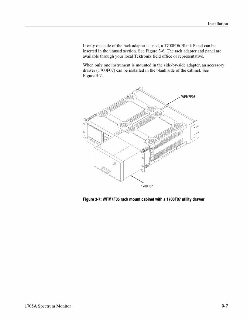
Installation
1705A Spectrum Monitor 3- 7
If only one side of the rack adapter is used, a 1700F06 Blank Panel can beinserted in the unused section. See Figure 3-6. The rack adapter and panel areavailable through your local Tektronix field office or representative.
When only one instrument is mounted in the side-by-side adapter, an accessorydrawer (1700F07) can be installed in the blank side of the cabinet. SeeFigure 3-7.
1700F07
WFM7F05
Figure 3-7: WFM7F05 rack mount cabinet with a 1700F07 utility drawer
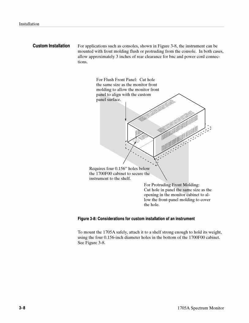
Installation
3- 8 1705A Spectrum Monitor
For applications such as consoles, shown in Figure 3-8, the instrument can bemounted with front molding flush or protruding from the console. In both cases,allow approximately 3 inches of rear clearance for bnc and power cord connec-tions.
Requires four 0.156” holes belowthe 1700F00 cabinet to secure theinstrument to the shelf.
For Flush Front Panel: Cut holethe same size as the monitor frontmolding to allow the monitor frontpanel to align with the custompanel surface.
For Protruding Front Molding:Cut hole in panel the same size as theopening in the monitor cabinet to al-low the front-panel molding to coverthe hole.
Figure 3-8: Considerations for custom installation of an instrument
To mount the 1705A safely, attach it to a shelf strong enough to hold its weight,using the four 0.156-inch diameter holes in the bottom of the 1700F00 cabinet.See Figure 3-8.
Custom Installation

Theory of Operation

1705A Spectrum Monitor 4- 1
Section 4Theory of Operation
The material in this section is subdivided into a general description (which issupported by the main block diagram) and detailed circuit descriptions that usethe schematic diagrams as illustrations. A thorough understanding of theinstrument starts with knowing how the major circuit blocks fit together,followed by an understanding of the individual circuit’s functions. Thesediscussions of the 1705A Spectrum Monitor begin with a brief, fundamentaloverview, then proceed on to the block diagram, and then into individual circuitdescriptions.
Overview
The 1705A Spectrum Monitor is a specialized spectrum analyzer, designed toassist in locating satellites, and to help optimize communication with thesatellite. It is capable of displaying the spectral plot of signals in the L--Band(900 -- 1750 MHz), and the 45 -- 100 MHz range on the crt. An alphanumericfrequency readout displays the frequency at the center of the intensified zone, inFULL SPAN/DIV, on the crt. In the magnified SPAN/DIV ranges, the frequencyreadout is the approximate frequency under the readout marker.
Front-panel mode switching is accomplished by push-button switches whosestatus is constantly polled by a microprocessor. In turn, the microprocessorcontrols switching functions and circuit gains so that the instrument can be usedto locate or monitor a specific set of frequencies.
The Low Voltage Power Supply is a high-efficiency switching type. The HighVoltage Power Supply provides 13 kV acceleration potential.
Block Diagram
The 1705A has two separate signal inputs, L--Band (Sweep range 900 --2000 MHz, calibrated range 900 -- 1750 MHz) and 70 MHz (45 -- 100 MHz).Selection of the frequency band to be displayed is accomplished by pushing afront-panel, momentary, push-button switch, which is monitored and acted uponby the microprocessor. When one input is selected, the other has its supplyvoltage interrupted.
The L--Band Tuner is self contained and consists of an RF Amplifier, VoltageControlled Oscillator, and a mixer stage. The gain, at the 1st IF frequency of489.9 MHz, is ¶10 dB. Both RF and IF gain can be adjusted. Its VCO is
RF Input Circuits(Diagram 1)
Theory of Operation
4- 2 1705A Spectrum Monitor
driven with a pre-corrected sweep ramp. Pre-correction is required to make upfor the inherent VCO nonlinearity.
A +18 V supply is connected to the L--BAND input connector so that it can beused to power a Block Down Converter (usually at the antenna). The supply canbe switched on and off by a recessed slide switch on the rear panel. The voltageis generated on a separate circuit board that is mounted inside the 1705A rearpanel.
The L--Band Tuner output passes through a 1st IF filter which contains a notch at590 MHz to eliminate a spurious mixing product. It is then mixed with an L.O.of 359.4 MHz to produce a 2nd IF output at 130.5 MHz. This output isamplified by an 8 dB gain MMIC and is combined with the 70 MHz tuneroutput.
The 70 MHz input consists of a 7-pole, 120 MHz, bandwidth low-pass filter; aVCO (which, like the L--Band VCO, is driven by a pre-corrected sweep ramp); amixer; and a 20 dB amplifier. The 70 MHz input circuits also output a 136 MHz1st IF with a gain of 0 dB ±3 dB.
The 136 MHz 2nd IF is converted a third time to produce a 3rd IF frequency of10.7 MHz. The crystal-controlled Local Oscillator operates at 119.8 MHz toprovide the 10.7 conversion. The oscillator’s output is tripled to 359.4 MHz toprovide the 130.5 MHz conversion for the L--Band Tuner output. A three-sec-tion helical resonator is used for the 130.5 MHz IF filter.
An additional band-pass crystal filter, centered at 10.7 kHz, with a 10 kHzbandwidth, can be added by front-panel selection, to provide narrow resolution.The 300 kHz bandwidth filter is always in the circuit regardless of the front-pa-nel RESOLUTION selection. Maximum bandwidth of the 1705A is 300 kHz.
The resolution filters drive a FSK receiver IC. Only the meter output of this ICis used to provide a voltage proportional to the log of the input power. Thisdrives a selectable video filter and the Vertical Deflection Amplifier.
The output of the Ramp Generator drives the Horizontal Deflection Amplifier(Diagram 4), Gain Control (SPAN/DIV), and the Marker Generator. The RampGenerator free runs with its repetition rate controlled by the front-panel SWEEPSPEED control. The amplitude of the ramp remains constant.
The Gain Control, which provides the ramp that is eventually used to drive theVCOs, consists of an operational amplifier with selectable input resistances. Theresistance selected is dependent upon the SPAN/DIV setting selected from thefront panel. The output ramp from the Gain Control circuit drives the SweepShapers.
The CENTER FREQUENCY control provides an offset to the sweep ramps inall SPAN/DIV settings except FULL. In the FULL SPAN/DIV setting, a
IF Amplifier Circuits(Diagram 2)
Sweep Generator Circuits(Diagram 3)
Test Equipment Depot - 800.517.8431 - 99 Washington Street Melrose, MA 02176 - FAX 781.665.0780 - TestEquipmentDepot.com
Theory of Operation
1705A Spectrum Monitor 4- 3
bright-up signal, centered around the center frequency, is generated for theZ--Axis Control circuit by the Marker Generator.
The Z--Axis Control circuit provides the driving signal for the Z--Axis Amplifier(Diagram 8). Included in these unblanking signals are the sweep unblanking,readout unblanking, and the intensified marker. This circuit controls bothdisplay and readout intensity and adding the intensified marker in FULLSPAN/DIV.
The output signal from the Log Detector (Diagram 2) is buffered and switched inand out, for time sharing with the readout signal, prior to driving the VerticalOutput Amplifier. The output amplifier normalizes gain and matches the crtdeflection plate input impedance.
The ramp signal from the Sweep Generator (Diagram 3) is buffered, inverted,and has its gain set prior to being used to drive the Horizontal Output Amplifier.Like the Vertical Output Amplifier, the readout signal is time shared with activesignal. The horizontal amplifier has approximately three times the gain of thevertical amplifier to meet the crt gain requirements.
The microprocessor, along with the EPROM that contains the measurement anddiagnostic routines, is the controlling element of the 1705A. A Non-VolatileRandom Access Memory (NVRAM) provides a method to store the currentfront-panel switch settings, at power down, so that the 1705A can come back upwith the last front-panel setup.
CENTER FREQUENCY readout data is converted to digital data by anAnalog-to-Digital Converter and then input into the microprocessor. Readoutdata and the Readout Enable (/RO--EN) are output from the microprocessor. Thereadout data is converted back to an analog signal by the Digital-to-AnalogConverter.
All of the switching and external control for the 1705A is shown on thisdiagram. Control voltages are limited to 11.8 V or less. All switching is done inconjunction with the microprocessor (Diagram 5). Indicator lights, that arecontrolled by the microprocessor, are also included on this diagram.
The +18 V supply that is designed to drive an external Block Down Converter isalso shown on this schematic. The On/Off switch for the +18 V supply islocated on the 1705A rear panel.
The Low Voltage Power Supply converts the mains ac line voltage to 4 dc outputvoltages (--15 V, +5 V, +15 V, and +40 V). The +40 V is used to power theVertical Deflection Amplifier (Diagram 4). The + and --15 V supplies are post
Deflection Amplifiers(Diagram 4)
Microprocessor(Diagram 5)
Front Panel (Diagram 6)
Low Voltage Power Supply(Diagram 7)
Theory of Operation
4- 4 1705A Spectrum Monitor
regulated to become the + and --11.8 V supplies on the Main circuit board(regulator circuits are on Diagram 4).
The Power Supply schematic also contains the 11.8 V Post Regulators, whoseoutputs are used by most of the circuits on the Main circuit board. The PostRegulators do not appear on the block diagram.
The unblanking signal from the Z--Axis Control drives the Z--Axis Amplifier.The Focus Amplifier, controlled by the front-panel control, provides a voltage tothe crt focus ring. The crt is of the Post Acceleration type, which requires arelatively high potential difference between the cathode and post anode. Theboost in 2nd anode voltage is provided by an encapsulated 4X Multiplier.
The High Voltage supply also provides the +100 V, required by the HorizontalDeflection Amplifier (Diagram 4), to drive the crt horizontal deflection plates.
RF InputDiagram 1
This diagram has both RF inputs for the Spectrum Monitor. The L--Band and70 MHz inputs are both off-board subassemblies. The 70 MHz input consists ofdiscrete components on a small circuit board that is totally shielded. TheL--Band Tuner is also self contained, totally shielded, and contains no user-ser-viceable parts.
The L--Band signal (900 -- 1750 MHz) is input directly to a tuner subassemblythat contains the Tuned RF Amplifier, mixer, and Voltage Controlled Oscillator(VCO) required to produce the first Intermediate Frequency (IF) of 489.9 MHz.The 489.9 MHz 1st IF signal is cabled to the Main board.
The tuner subassembly is powered by the +11.8 volts, which is controlled by theInput Switching. (The +11.8 V to the L--Band Tuner is disabled when the70 MHz input is selected.) In addition, the Block Down Converter +18 V supply(from Diagram 5) is fed to the tuner for output on its F-type connector. Arecessed, rear-panel slide switch connects the +18 V supply to the L--Band Tuner.A pre-corrected ramp (from Diagram 3) to drive the VCO is also supplied to thetuner subassembly.
The /LBAND control line, from the microprocessor, is low when the L--Band isselected. When /LBAND goes high (indicating that the 70 MHz input has beenselected) Q31 turns on and Q30 turns off, causing Q32 to turn off and disconnectthe +11.8 V from the tuner.
The input to the 70 MHz tuner has a 75Ω, 10 dB pad, which allows it to acceptsignals up to --20 dBm. The 70 MHz signal (45 -- 100 MHz) is preconditioned
High Voltage (Diagram 8)
L- Band Input
70 MHz Input
Theory of Operation
1705A Spectrum Monitor 4- 5
by a 7-pole, 120 MHz, low-pass filter that rejects out-of-band frequencies. TheMixer, U190, with input frequencies of 45 -- 100 MHz, and the Local Oscillatoroperating at [Fi + 130 MHz] provide a 130 MHz 1st IF. The signal output fromthe Mixer is terminated by a 75Ω, 3 dB pad made up of R291, R292, and R293.The IF signal is ac coupled into the amplifier, U296, with a gain of 20 dB.R396, R391, and R392 form a 6 dB pad that outputs the 136 MHz 1st IF signalthat approximates the L--Band output level for inputs 10 dB higher.
L393, L391, L389, C292, and C290 form a low-pass filter that is peaked at the1st IF frequency (136 MHz) and approximately 20 dB down at the LocalOscillator frequency. Harmonics of the Local Oscillator frequency are at least30 dB down.
The Local Oscillator (LO) is a Voltage Controlled Oscillator (VCO) whoseoutput frequency range is 175 MHz to 230 MHz. The oscillator is a differentialpair (pins 7--8 and 5--11) contained in U283. The oscillator employs positivefeedback through L284 to the base tank circuit (L280 and C281). CR280 is avaractor whose capacitance is determined by the instantaneous level of thepre-corrected ramp from the Sweep Generator (Diagram 3). The center tap ofT187 is the LO output providing an amplitude of approximately +7 dBm.
Q20 and Q21 form a switching circuit that turns off the VCO when the L--Bandinput is selected. When /LBAND goes low, Q21 is shut off, causing Q20 tounsaturate and disconnect the --11.8 V from the VCO.
The 70 MHz tuner assembly (A5) is contained in a rigidly mounted shield.Control signals and the --11.8 V supply are brought into this shielded tunerthrough feedthrough capacitors.
IF AmplifierDiagram 2
This diagram shows the L--Band and 70 MHz inputs to the various conversionstages. It also shows the Local Oscillator/Tripler circuitry, Mixers, Amplifiers,IF filters, and Log Detector output.
Both Local Oscillator (LO) signals are derived from a single crystal, whoseoperating frequency is 119.8 MHz. The crystal is a 5th overtone type in a Butleroscillator configuration using Q13. Q11 buffers the oscillator and drives a 3 dBisolation pad on the LO input of Double Balanced Mixer (DBM) U25. Q12 is acascode stage driving a tank circuit at the 3rd harmonic (359.4 MHz). The tankcircuit is tapped down to drive a three-section helical resonator, FL1, tuned to359.4 MHz. The output from FL1 is coupled into DBM U28.
70 MHz Local Oscillator
2nd Local Oscillator
Theory of Operation
4- 6 1705A Spectrum Monitor
DBM U28 is driven by the L--Band Tuner output at 489.9 MHz through aLPF/Notch filter consisting of L11, L12, and series resonant circuit C69 andW13. W13 is a shorted length of 50Ω coax forming a high-Q inductor. Thisprovides a narrow notch at 590 MHz to eliminate a spurious output from theL--Band Tuner.
The output from DBM U28 drives U31 which provides about 8 dB gain tocompensate for the mixer loss and optimize the system dynamic range. Thissignal is then combined with the 70 MHz tuner output with 3 dB combiner T1.
The band-pass filter, FL2, is a three-section helical resonator with about 8 MHzbandwidth.
U25 is a double balanced mixer that converts the 130.5 MHz 2nd IF frequency tothe 10.7 MHz 3rd IF frequency. The LO frequency (119.8 MHz) is below the2nd IF frequency by the 3rd IF frequency. J6 is a test jumper that can be lifted toevaluate prior circuitry or to insert a signal at the 3rd IF frequency to trouble-shoot the circuits that follow.
The 2nd IF Amplifier, U22, has a gain of 20 dB. U22 requires a 6 V Vcc; VR3and R136 are used to derive the voltage from the +11.8 V supply. C31 and C32are decoupling capacitors. The output signal level is --20 dBm maximum. J5 isanother test jumper that can be used to access prior circuits or insert a signal atthe 2nd IF frequency.
The 10.7 MHz 2nd IF signal passes through the 300 kHz Resolution filter or acombination of the 10 kHz and the 300 kHz Resolution filters. The switching offilters is accomplished by a combination of a control signal (/10KHZ) from themicroprocessor (Diagram 5) and a switching network consisting of U23D, E, andF, Q9, and Q10, and switching diodes (CR22, 23, 25, 26, 27, 28, 29, and 30).When the control line is low, the signal path is through the 10 kHz filter. The300 kHz filter is always in the circuit. Q10, CR22, and CR30 turn on to enablethe 10 kHz filter; Q9, CR23, and CR28 turn off to switch out the bypass line.When the control line goes high, Q10 turns off to turn off CR22 and CR30; Q9,CR23, and CR28 turn on to shunt the 10 kHz filter and provide 300 kHzresolution. R175, the 300 kHz Gain adjustment, is set to match the loss of the10 kHz filter. J10 is another test jumper provided to access prior circuits orinsert a signal directly into the Log Detector.
The input to the Log Detector, U32, is amplified by U29 and pre-shaped by FL3and FL4, a 300 kHz Resolution filter, and then ac coupled to U32. When the10 kHz filter is selected, the signal is filtered by the 10 kHz filter and thenapplied to the Log Detector. The output current from the Log Detector isprocessed by Q24 and Q25 to the 15 kHz low-pass filter at U27 pin 3 (Dia-gram 4). The filter output then drives the Vertical Deflection Amplifier.
Input Filter, Mixer, and IFAmplifier
Resolution Filter and LogDetector
Theory of Operation
1705A Spectrum Monitor 4- 7
Sweep GeneratorDiagram 3
This schematic contains the free--running Ramp Generator, Switchable GainControl (SPAN/DIV), Sweep Shapers, Marker Generator, and the Z--Axis(Brightness) control.
U24 is the Ramp Generator; U24B is configured as an integrator and U24A isused as a comparator. C40 is the integration capacitor and is charged by currentfrom the front-panel SWEEP SPEED control. The ramp integrates in thepositive direction from --2 volts to +2 volts. At +2 V the output of U24A trips tothe positive power supply voltage (+5 V) and causes C40 to ramp down throughCR24 and R151. The value of R151 determines the amount of time required todischarge C40 (retrace time). The power supply for U24 is +5 and --11.8 volts.The output swing of U24A is nearly to these supply values. The RampGenerator output, through R142, drives Q6 through U23B in the Z--Axis controlto provide retrace blanking. CR21 limits the output swing in the negativedirection to --0.7 volts.
The Ramp Generator output (U24B, pin 7) drives the Horizontal DeflectionAmplifier and the Gain Control (SPAN/DIV) switching, U20. Each switch inU20 selects a different value of Ri for operational amplifier U18A. The gain ismaximum at FULL (50 MHz per division) and minimum at 100 kHz perdivision. The output of U18A is a negative-going ramp that drives the SweepShapers.
U16B and C form the Sweep Shaper that drives the L--BAND VCO; U16A andD drive the 70 MHz VCO. The Sweep Shapers pre-distort the VCO drivingramps to compensate for the inherent nonlinearity of the VCO. The shapers haveadjustable break points so that gain at each can be individually adjusted. The70 MHz shaper has four adjustments, R48, R49, R55, R56; and the L--BANDshaper has six adjustments, R35, R51, R58, R75, R81, and R82. Figure 4-1shows the area of control for the various adjustments on the 1705A L--Banddisplay, when a comb signal is applied.
Ramp Generator
Gain Control (SPAN/DIV)
Sweep Shapers
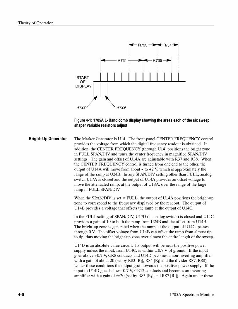
Theory of Operation
4- 8 1705A Spectrum Monitor
STARTOF
DISPLAY
R727 R729
R737R733
R731 R735
Figure 4-1: 1705A L-Band comb display showing the areas each of the six sweepshaper variable resistors adjust
The Marker Generator is U14. The front-panel CENTER FREQUENCY controlprovides the voltage from which the digital frequency readout is obtained. Inaddition, the CENTER FREQUENCY (through U14) positions the bright zonein FULL SPAN/DIV and tunes the center frequency in magnified SPAN/DIVsettings. The gain and offset of U14A are adjustable with R37 and R38. Whenthe CENTER FREQUENCY control is turned from one end to the other, theoutput of U14A will move from about -- to +2 V, which is approximately therange of the ramp at U24B. In any SPAN/DIV setting other than FULL, analogswitch U17A is closed and the output of U14A provides an offset voltage tomove the attenuated ramp, at the output of U18A, over the range of the largeramp in FULL SPAN/DIV
When the SPAN/DIV is set at FULL, the output of U14A positions the bright-upzone to correspond to the frequency displayed by the readout. The output ofU14B provides a voltage that offsets the ramp at the output of U14C.
In the FULL setting of SPAN/DIV, U17D (an analog switch) is closed and U14Cprovides a gain of 10 to both the ramp from U24B and the offset from U14B.The bright-up zone is generated when the ramp, at the output of U14C, passesthrough 0 V. The offset voltage from U14B can offset the ramp from almost tipto tip, thus moving the bright-up zone over almost the entire length of the sweep.
U14D is an absolute value circuit. Its output will be near the positive powersupply unless the input, from U14C, is within ±0.7 V of ground. If the inputgoes above +0.7 V, CR8 conducts and U14D becomes a non-inverting amplifierwith a gain of about 20 (set by R83 [Rf], R84 [Ri] and the divider R87, R88).Under these conditions the output goes towards the positive power supply. If theinput to U14D goes below --0.7 V, CR12 conducts and becomes an invertingamplifier with a gain of¶20 (set by R83 [Rf] and R87 [Ri]). Again under these
Bright- Up Generator
Theory of Operation
1705A Spectrum Monitor 4- 9
conditions the output goes toward the positive supply. If the input is between +and --0.7 V, neither diode conducts and the amplifier has no input and, conse-quently, an output of 0 V. When the output of U14D is near 0 V, a pulse thatproduces the crt bright zone is generated by the Z--Axis Control circuit.
The Z--Axis Control circuit is comprised of a transistor array, U13, and discretetransistors Q4 and Q5. The output is the common collector line of the threedifferential amplifiers (Q5, and pins 5 and 8 of U13). The output line drives thesumming junction of the Z--Axis Amplifier on Diagram 8. The front-panelINTENSITY control drives the current source (pins 12, 13, and 14 of U13). Allof the current from this transistor can be directed to the Z--Axis Amplifier,through the differential amplifiers or shunted away if Q6 is turned on. Q6 is onduring sweep retrace, to blank the crt, and during crt readout time, when/RO--EN is active (low). With Q6 off, the current from the source is splitbetween R54 and R79. The current through R54 is the collector current on pin 5.The current through R79 will appear as collector current on pin 8 if its base(pin 9) is low, which occurs at marker time. The result is that when theinstrument is in FULL SPAN, the trace is brightened for the marker. In anyother SPAN/DIV setting, the trace is of uniform brightness when the output ofU14D is near 0 V, a pulse that produces the crt bright zone is generated by theZ--Axis Control circuit.
The readout intensity is controlled separately by Q4 and Q5. If the RO--BLANKcontrol line is active (low), Q4 is turned off and Q5 is turned on. When Q5 ison, the current through R89 and R91 is sent to the Z--Axis Amplifier. When thecontrol line goes high, Q4 turns on and the emitter current from the readoutintensity control is directed into the +5 volt supply instead of into the Z--AxisAmplifier.
Deflection AmplifiersDiagram 4
Circuitry on this schematic normalizes gains, and drives the crt deflection plates.
The vertical signal from the Log Detector is buffered by U27. U27 drives theVertical Output Amplifier, whose input can be filtered to reduce the effects ofnoise. The Video Filter is a 15 kHz, 3-pole, low-pass filter whose output isswitched in by U30A. The enable, for U30A, is the /VFILTER signal from themicroprocessor (Diagram 5).
U27 is a switchable gain amplifier. When high gain (2 dB/Div) is selected withthe front-panel push button, the signal at pin 12 of the microprocessor (U2) goeshigh, and the switch in U21C grounds R135 through pins 3 and 4. Thisincreases the gain of U27 by approximately a factor of five. U21A alsoswitches, connecting pins 13 and 14, putting a portion of the Vertical Position
Z- Axis Control
Buffers
Theory of Operation
4- 10 1705A Spectrum Monitor
control into the summing junction of U27 (pin 2). The Vertical Position controlis attenuated by resistors R152 and R140 (2 dB POS RANGE). This positionsthe video signal at pin 6 of U27, providing greater positioning range while inHigh Gain mode.
The horizontal ramp signal from the Sweep Generator (Diagram 3) is approxi-mately 4 V in amplitude. Typical sweep length is 12 divisions. The variableresistor, R168, is one-half of the input resistance (Ri) for U26B, an invertingoperational amplifier. The amplifier feedback resistance (Rf) consists of R180and R177. Reducing the Rf of the operational amplifier while holding Ri
constant reduces the gain, and in this case the sweep length. Strapping acrossW11 and W12 provides a convenient method of shortening the sweep to adjustthe Horizontal Gain (R168) against the 10 divisions of the crt graticule. Whenthe strap is removed the sweep length increases to 12 divisions.
Switches U30B and C are are enabled by the Readout Enable (/RO--EN) from themicroprocessor (Diagram 5). When enabled, the input to the DeflectionAmplifier is the X-- (horizontal) and Y--Axis (vertical) components of the crtalphanumeric readout. The readout signal components are from the microproces-sor through a Digital-to-Analog Converter (DAC) (Diagram 5). The verticalpositioning signal, from the front-panel VERTICAL POSITION control, isapplied to the readout in order to common mode out positioning effect when thetrace is repositioned.
The vertical output signal, or the Y--Axis readout, drives the base of Q26, oneside of a differential input amplifier. The other side, Q28, is driven by thepositioning voltage from the front-panel VERTICAL POSITION control. Thesignal from the collectors of Q26 and Q28 drive Q27 and Q29, common baseamplifier stages. The gain of the Vertical Deflection Amplifier is approximately7. The gain normalized output voltage, to drive the crt deflection plates, isdeveloped across R229 and R230, the load resistors. Q22 and Q23 are atemperature-compensated current source from the --11.8 volt supply.
Sweep ramp or X--Axis readout drives the base of Q17, one side of a differentialinput amplifier. The other side, Q16, is driven by the positioning voltage fromthe front-panel HORIZONTAL POSITION control (Diagram 5). The signalfrom the collectors of Q17 and Q16 drive Q14 and Q15, common base amplifierstages. The gain of the Horizontal Deflection Amplifier is approximately 20.The gain normalized output voltage, to drive the crt deflection plates, isdeveloped across load resistors R178 and R179. Q18 and Q19 are a temperature-compensated current source from the --11.8 volt supply.
Vertical DeflectionAmplifier
Horizontal DeflectionAmplifier
Theory of Operation
1705A Spectrum Monitor 4- 11
MicroprocessorDiagram 5
The 1705A is a microprocessor-controlled instrument. Circuitry on Diagram 5shows the microprocessor, the front-panel LED drive, the crt readout drive, thegraticule light circuit, and the trace rotation circuit.
The processor (U2) is an 8-bit, 3-port microprocessor running at 12 MHz. U8 isthe lower order address de-multiplexer for the Program PROM U9. U9 is a 64KUV Erasable CMOS PROM. R5 is the bus termination assuring TTL levels (0=0 V, 1 = 5 V). Output enable for the PROM is the PSEN output from themicroprocessor (U2, pin 29). The lower-order addresses from the processor(AD0 -- AD7), which are de-multiplexed by U8, are from Port 0; the higher-orderaddresses (AD8 -- AD12) are from Port 2. The higher-order addresses are notmultiplexed.
Port 1 is a multifunction input/output port. Lines 0 through 4 are used to poll thefront-panel push-button switches (momentary ground closures) to set up themeasurement program. Line 6 outputs the clock (U2, pin 7) that is used by theReadout DAC and the NVRAM (Non-Volatile Random Access Memory).Line 5 is the data transfer (U2, pin 6) for the NVRAM, U4. The Readout Enable(/RO--EN) that turns on the crt readout is output through Line 7 (U2, pin 8). TheCenter Frequency Readout data from U1, the readout ADC, is input throughLine 5 also (U2, pin 6).
U1 is an A-to-D Converter (ADC), with successive approximation register. It isused to convert the analog voltage level from the front--panel CENTERFREQUENCY control to a digital signal for the microprocessor and the ReadoutDigital-to-Analog Converter (DAC). R4 is the calibration adjustment to ensurecorrect readout.
U4 is the NVRAM that stores the instrument condition when power is turned offor lost, to ensure that the instrument will come back up in the correct operatingcondition. The power down detection circuit consists of a comparator, U11, anda +5 volt regulator, U3. U3 input voltage is from the +15 volt supply. C5charges up high enough to allow U3 to continue to power U11 so that it can storeneeded data during the power-down sequence. U11 monitors the +5 volt supplyon pin 2. Pin 3 is set to approximately 2.5 volts and has a large capacitor, C13,to provide a slow decay. Under normal conditions, pin 2 is slightly higher thanpin 3, keeping the output (pin 7) high. When instrument power starts to godown, pin 2 goes below pin 3, which forces the output (pin 7) low to enable the/STO input to U4. When /STO goes low, the current conditions, as input fromthe microprocessor D-Out output, are stored in the U4 Non-Volatile RAM.
Microprocessor
Theory of Operation
4- 12 1705A Spectrum Monitor
U6 is an 8-bit D-type data latch that drives all the front-panel LEDs and most ofthe internal control lines. Chip select for U6 is /WR (U2, pin 16) inverted (U7C)and ANDed with Address 14 (U2, pin 27) by U7A.
U10 is a dual 8-bit DAC (Digital-to-Analog Converter) that generates thehorizontal and vertical readout signals. The analog current outputs of U10 arepins 2 and 20, which are converted to voltage by U12 A and B. Chip select is/WR (U2, pin 16) which is inverted (U7C) and ANDed with Address 7 in U7D.Line A0 from U8, pin 19, is the DAC A select (low enable). U5 provides a--5 volt analog voltage reference for U10.
Trace rotation compensates for changes in the magnetic field surrounding the1705A. Q1 and Q2 are emitter followers that provide the Trace Rotation currentto a coil around the crt, inside the shield. The voltage on the emitter of either Q1or Q2 will develop a current through R19 to drive the coil. Current amplitudeand polarity are controlled by the front-panel TRACE ROTATION screwdriveradjustment.
Q3 and Q100 provide a current source for the graticule lights. Base voltage,which controls the amount of current flowing in the light circuit, is set by thefront-panel SCALE control. Jumper J100 on the Graticule Light board allowsthe graticule lights to be disabled.
Front PanelDiagram 6
The front-panel schematic shows all of the operational controls for the instru-ment, including potentiometers, momentary push-button switches, and indicatorLEDs. All the push buttons are polled by the microprocessor, and the LEDs aredriven by output ports from the microprocessor. Also included on this diagramis the +18 volt Block Down Converter (BDC) power supply.
The front-panel LED indicators are returned to a current source (+5 V). When anLED is lighted, there is a complete circuit from the Light Driver (Diagram 5)through the LED to the +5 V supply. The five function switches (front-panelpush buttons) are simple ground closures that are read by the microprocessor todetermine the operating mode.
The eight front-panel controls determine voltages (in a range between --11.8 Vand +11.8 V) depending on circuit requirements. Each control works with aspecific circuit on another diagram.
Readout
Trace Rotate
Graticule Lights
Indicators, Controls, andSwitches
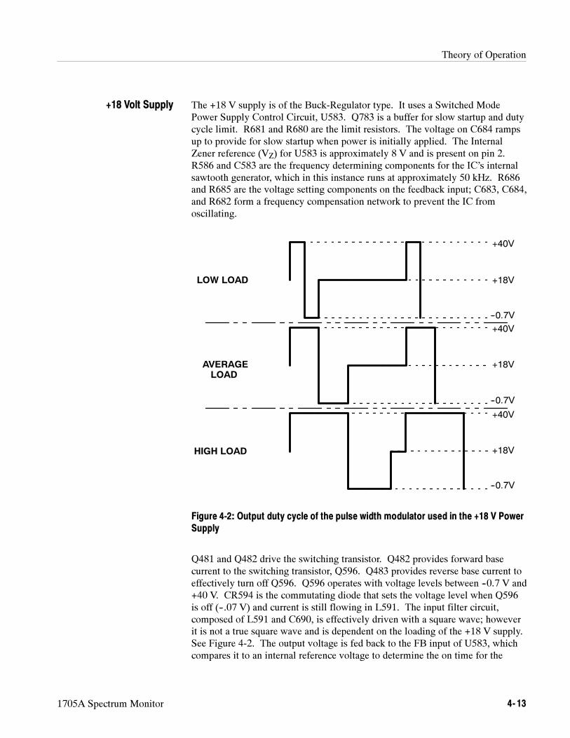
Theory of Operation
1705A Spectrum Monitor 4- 13
The +18 V supply is of the Buck-Regulator type. It uses a Switched ModePower Supply Control Circuit, U583. Q783 is a buffer for slow startup and dutycycle limit. R681 and R680 are the limit resistors. The voltage on C684 rampsup to provide for slow startup when power is initially applied. The InternalZener reference (VZ) for U583 is approximately 8 V and is present on pin 2.R586 and C583 are the frequency determining components for the IC’s internalsawtooth generator, which in this instance runs at approximately 50 kHz. R686and R685 are the voltage setting components on the feedback input; C683, C684,and R682 form a frequency compensation network to prevent the IC fromoscillating.
+40V
+40V
+40V
+18V
+18V
+18V
--0.7V
--0.7V
--0.7V
LOW LOAD
AVERAGELOAD
HIGH LOAD
Figure 4-2: Output duty cycle of the pulse width modulator used in the +18 V PowerSupply
Q481 and Q482 drive the switching transistor. Q482 provides forward basecurrent to the switching transistor, Q596. Q483 provides reverse base current toeffectively turn off Q596. Q596 operates with voltage levels between --0.7 V and+40 V. CR594 is the commutating diode that sets the voltage level when Q596is off (--.07 V) and current is still flowing in L591. The input filter circuit,composed of L591 and C690, is effectively driven with a square wave; howeverit is not a true square wave and is dependent on the loading of the +18 V supply.See Figure 4-2. The output voltage is fed back to the FB input of U583, whichcompares it to an internal reference voltage to determine the on time for the
+18 Volt Supply
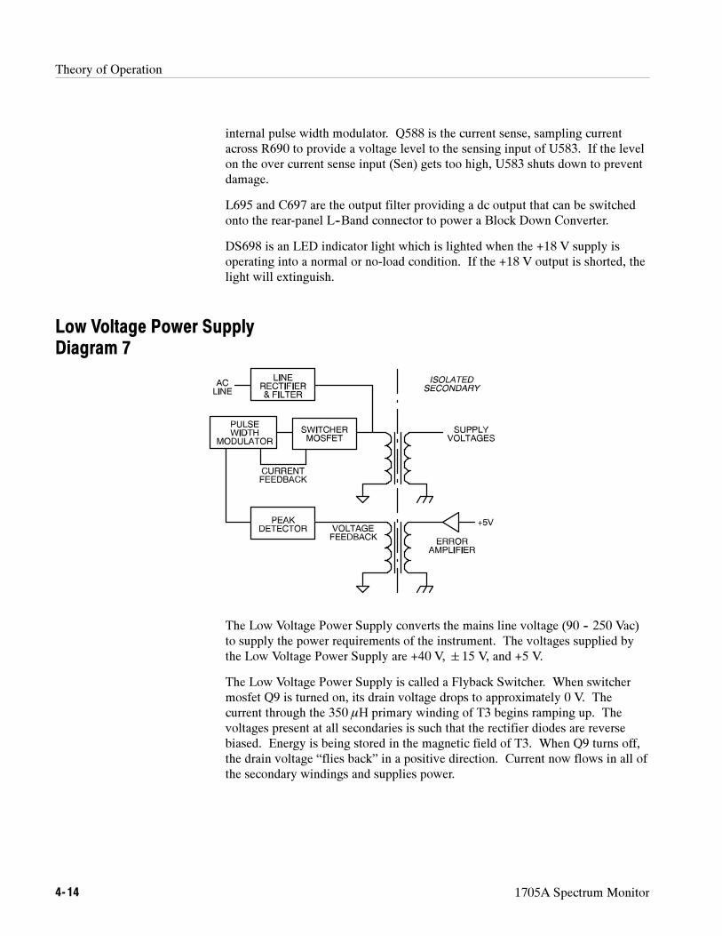
Theory of Operation
4- 14 1705A Spectrum Monitor
internal pulse width modulator. Q588 is the current sense, sampling currentacross R690 to provide a voltage level to the sensing input of U583. If the levelon the over current sense input (Sen) gets too high, U583 shuts down to preventdamage.
L695 and C697 are the output filter providing a dc output that can be switchedonto the rear-panel L--Band connector to power a Block Down Converter.
DS698 is an LED indicator light which is lighted when the +18 V supply isoperating into a normal or no-load condition. If the +18 V output is shorted, thelight will extinguish.
Low Voltage Power SupplyDiagram 7
The Low Voltage Power Supply converts the mains line voltage (90 -- 250 Vac)to supply the power requirements of the instrument. The voltages supplied bythe Low Voltage Power Supply are +40 V, 15 V, and +5 V.
The Low Voltage Power Supply is called a Flyback Switcher. When switchermosfet Q9 is turned on, its drain voltage drops to approximately 0 V. Thecurrent through the 350 H primary winding of T3 begins ramping up. Thevoltages present at all secondaries is such that the rectifier diodes are reversebiased. Energy is being stored in the magnetic field of T3. When Q9 turns off,the drain voltage “flies back” in a positive direction. Current now flows in all ofthe secondary windings and supplies power.
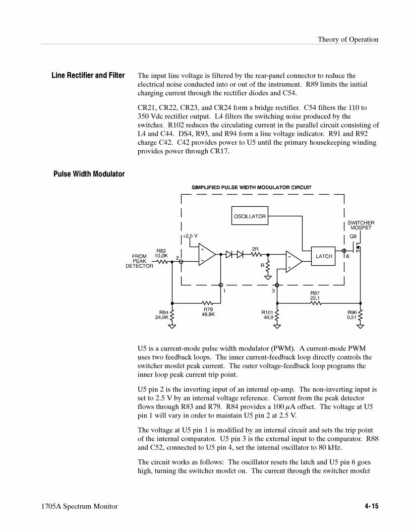
Theory of Operation
1705A Spectrum Monitor 4- 15
The input line voltage is filtered by the rear-panel connector to reduce theelectrical noise conducted into or out of the instrument. R89 limits the initialcharging current through the rectifier diodes and C54.
CR21, CR22, CR23, and CR24 form a bridge rectifier. C54 filters the 110 to350 Vdc rectifier output. L4 filters the switching noise produced by theswitcher. R102 reduces the circulating current in the parallel circuit consisting ofL4 and C44. DS4, R93, and R94 form a line voltage indicator. R91 and R92charge C42. C42 provides power to U5 until the primary housekeeping windingprovides power through CR17.
U5 is a current-mode pulse width modulator (PWM). A current-mode PWMuses two feedback loops. The inner current-feedback loop directly controls theswitcher mosfet peak current. The outer voltage-feedback loop programs theinner loop peak current trip point.
U5 pin 2 is the inverting input of an internal op-amp. The non-inverting input isset to 2.5 V by an internal voltage reference. Current from the peak detectorflows through R83 and R79. R84 provides a 100 A offset. The voltage at U5pin 1 will vary in order to maintain U5 pin 2 at 2.5 V.
The voltage at U5 pin 1 is modified by an internal circuit and sets the trip pointof the internal comparator. U5 pin 3 is the external input to the comparator. R88and C52, connected to U5 pin 4, set the internal oscillator to 80 kHz.
The circuit works as follows: The oscillator resets the latch and U5 pin 6 goeshigh, turning the switcher mosfet on. The current through the switcher mosfet
Line Rectifier and Filter
Pulse Width Modulator
Theory of Operation
4- 16 1705A Spectrum Monitor
increases, causing the voltage across R96 to increase. This voltage is divided byR87 and R101, and is applied to the comparator (pin 3). When the voltage at U5pin 3 reaches the comparator trip point, the latch toggles and the switcher mosfetis turned off. This process is repeated at an 80 kHz rate.
C58 increases the PWM noise immunity by rolling off the internal op-ampfrequency response. R82 holds the switcher mosfet off as the circuit is poweringup. R81 slows the turn-on of the switcher mosfet while CR27 speeds up the turnoff.
The three output windings supply four output voltages. Each output is rectifiedby a single diode and filtered by an LC pi filter.
The Error Amplifier regulates the +5 V output by feeding an error signal to thePulse Width Modulator. VR1 is a 2.5 V shunt regulator containing an op-ampand a voltage reference. The +5 V is divided by R69 and R70 to provide 2.5 Vto VR1, with fine adjustment provided by R99. C40 and R71 determine the gainand frequency response of VR1. VR4 controls overshoot of the +5 V at powerup. R98 and CR26 provide a minimum operating current for VR1. R68decouples C39 from VR1. Overvoltage protection for the +5V supply isprovided by a crowbar circuit formed by Q11, VR3, R13, and R14.
The 80 kHz sawtooth waveform at U3 pin 3 trips comparator U3. U3 pin 1 thenfeeds a trigger pulse to one-shot U4. U4 pin 13 outputs a 300 nS pulse to the130 mA current source consisting of Q7 and Q8. When Q8 turns on, T2 pin 2 ispulled down until CR15 (Error Amplifier) is forward biased. The negative-goingpulse at T2 pin 2 is peak detected by CR16 and C46. The dc voltage present atthe anode of CR16 feeds the pulse width modulator and the Output Under-Volt-age Shutdown circuit. CR29 resets T2 between pulses.
If the +5 V is below 4.9 V, the Error Amplifier will cause the Peak Detectoroutput to go below 2.9 V. The output of comparator U3B will pull low and shutdown pulse width modulator U5. C47 and R96 delay the operation of U3B longenough for the power supply to power up. If the +5 V does not reach 4.9 Vwithin 50 ms of power up, U3B will shut down the switcher. The power supplywill then cycle on and off every couple of seconds.
Output Filters
Error Amplifier
Feedback TransformerDriver and Peak Detector
Output Under-VoltageShutdown
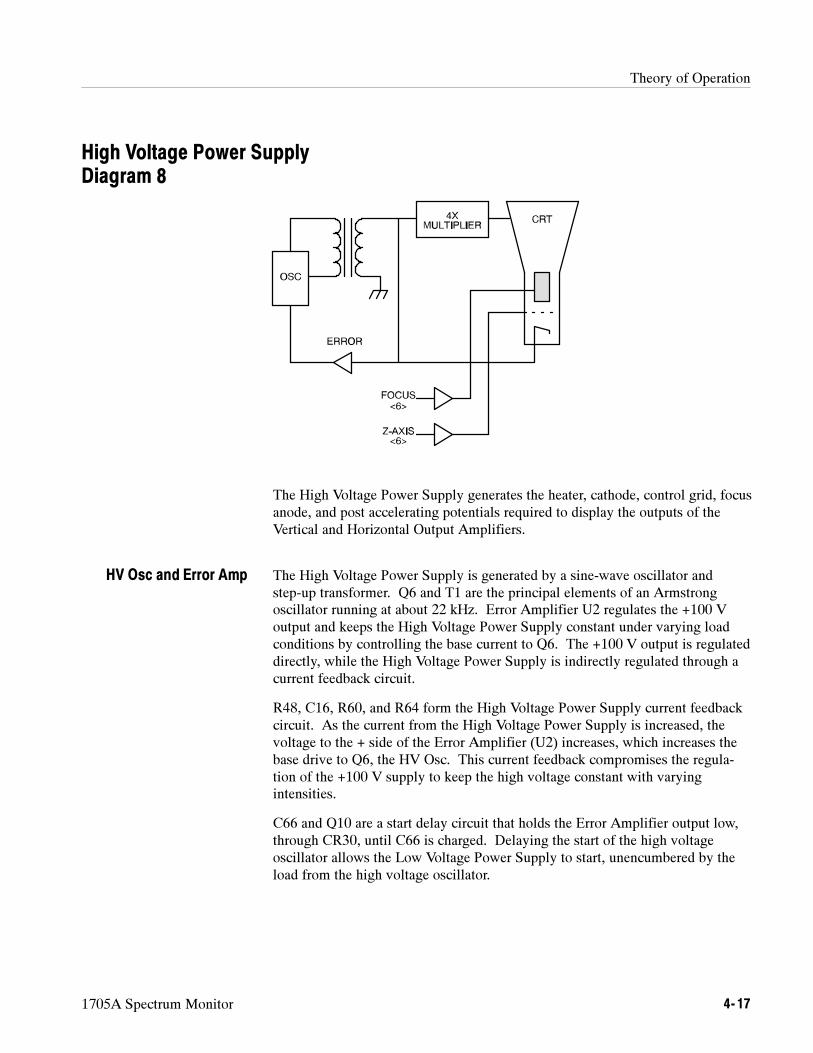
Theory of Operation
1705A Spectrum Monitor 4- 17
High Voltage Power SupplyDiagram 8
The High Voltage Power Supply generates the heater, cathode, control grid, focusanode, and post accelerating potentials required to display the outputs of theVertical and Horizontal Output Amplifiers.
The High Voltage Power Supply is generated by a sine-wave oscillator andstep-up transformer. Q6 and T1 are the principal elements of an Armstrongoscillator running at about 22 kHz. Error Amplifier U2 regulates the +100 Voutput and keeps the High Voltage Power Supply constant under varying loadconditions by controlling the base current to Q6. The +100 V output is regulateddirectly, while the High Voltage Power Supply is indirectly regulated through acurrent feedback circuit.
R48, C16, R60, and R64 form the High Voltage Power Supply current feedbackcircuit. As the current from the High Voltage Power Supply is increased, thevoltage to the + side of the Error Amplifier (U2) increases, which increases thebase drive to Q6, the HV Osc. This current feedback compromises the regula-tion of the +100 V supply to keep the high voltage constant with varyingintensities.
C66 and Q10 are a start delay circuit that holds the Error Amplifier output low,through CR30, until C66 is charged. Delaying the start of the high voltageoscillator allows the Low Voltage Power Supply to start, unencumbered by theload from the high voltage oscillator.
HV Osc and Error Amp
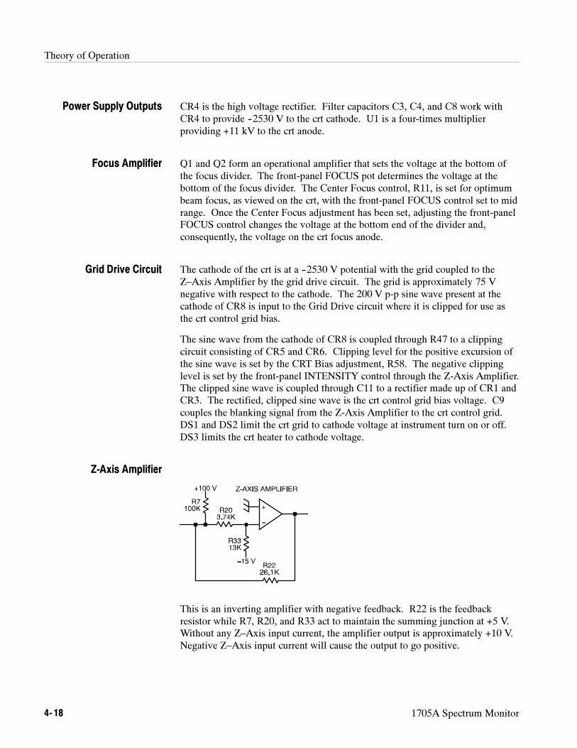
Theory of Operation
4- 18 1705A Spectrum Monitor
CR4 is the high voltage rectifier. Filter capacitors C3, C4, and C8 work withCR4 to provide --2530 V to the crt cathode. U1 is a four-times multiplierproviding +11 kV to the crt anode.
Q1 and Q2 form an operational amplifier that sets the voltage at the bottom ofthe focus divider. The front-panel FOCUS pot determines the voltage at thebottom of the focus divider. The Center Focus control, R11, is set for optimumbeam focus, as viewed on the crt, with the front-panel FOCUS control set to midrange. Once the Center Focus adjustment has been set, adjusting the front-panelFOCUS control changes the voltage at the bottom end of the divider and,consequently, the voltage on the crt focus anode.
The cathode of the crt is at a --2530 V potential with the grid coupled to theZ–Axis Amplifier by the grid drive circuit. The grid is approximately 75 Vnegative with respect to the cathode. The 200 V p-p sine wave present at thecathode of CR8 is input to the Grid Drive circuit where it is clipped for use asthe crt control grid bias.
The sine wave from the cathode of CR8 is coupled through R47 to a clippingcircuit consisting of CR5 and CR6. Clipping level for the positive excursion ofthe sine wave is set by the CRT Bias adjustment, R58. The negative clippinglevel is set by the front-panel INTENSITY control through the Z-Axis Amplifier.The clipped sine wave is coupled through C11 to a rectifier made up of CR1 andCR3. The rectified, clipped sine wave is the crt control grid bias voltage. C9couples the blanking signal from the Z-Axis Amplifier to the crt control grid.DS1 and DS2 limit the crt grid to cathode voltage at instrument turn on or off.DS3 limits the crt heater to cathode voltage.
This is an inverting amplifier with negative feedback. R22 is the feedbackresistor while R7, R20, and R33 act to maintain the summing junction at +5 V.Without any Z–Axis input current, the amplifier output is approximately +10 V.Negative Z–Axis input current will cause the output to go positive.
Power Supply Outputs
Focus Amplifier
Grid Drive Circuit
Z-Axis Amplifier
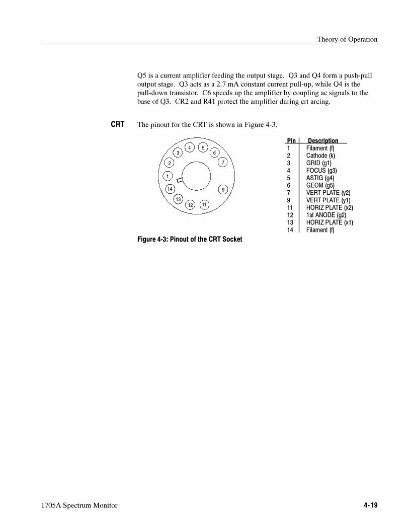
Theory of Operation
1705A Spectrum Monitor 4- 19
Q5 is a current amplifier feeding the output stage. Q3 and Q4 form a push-pulloutput stage. Q3 acts as a 2.7 mA constant current pull-up, while Q4 is thepull-down transistor. C6 speeds up the amplifier by coupling ac signals to thebase of Q3. CR2 and R41 protect the amplifier during crt arcing.
The pinout for the CRT is shown in Figure 4-3.
Pin Description1 Filament (f)2 Cathode (k)3 GRID (g1)4 FOCUS (g3)5 ASTIG (g4)6 GEOM (g5)7 VERT PLATE (y2)9 VERT PLATE (y1)11 HORIZ PLATE (x2)12 1st ANODE (g2)13 HORIZ PLATE (x1)14 Filament (f)
14
13
12 11
9
7
6
54
3
2
1
Figure 4-3: Pinout of the CRT Socket
CRT

Theory of Operation
4- 20 1705A Spectrum Monitor

Checks and Adjustments

1705A Spectrum Monitor 5- 1
Section 5Checks And Adjustments
This section consists of two separate procedures. The first, a PerformanceCheck, is used to determine compliance with the Performance Requirements inthe Specification. The second is the Adjustment Procedure, that provides theinstructions on how to adjust the instrument and return it to operation within thespecification.
In both procedures, front- and rear-panel controls and connectors, on theinstrument under test, are fully capitalized (e.g., 300 kHz RESOLUTION).Control and connector names on test equipment and internal controls andadjustments for the instrument under test are initial capitalized (e.g., Time/Div,Geometry, etc.).
Limits, tolerances, and waveforms given in this section are guides to adjustmentsand checks. They are not instrument specifications, except when listed in thePerformance Requirement column of the Specification Tables in Section 1 of thismanual.
Recommended Equipment List
The following equipment and accessory items are required to do the PerformanceCheck and/or Adjustment Procedures. Broad specifications are followed by apiece of equipment that meets these specifications; in most cases, the recom-mended instrument was used in preparing the procedures that follow.
1. Test Oscilloscope
Vertical Amplifier:
30 MHz Bandwidth, 1 mV Sensitivity.
Time Base:
10 ns/Division to 5 ms/Division sweep speeds, triggering to 5 MHz.
For example: a TEKTRONIX 7603 Oscilloscope with a 7A18 Dual-TraceAmplifier and a 7B53A Dual Time Base, or a TEKTRONIX 11403AOscilloscope with a 11A34V Video Amplifier and an 11T5H Video Trigger.Also a 10X probe, P6106 (Tektronix Part No. 010-6106-03).
Electrical Instruments
Checks and Adjustments
5- 2 1705A Spectrum Monitor
2. Leveled Sine Wave Generator, at least 250 kHz to 95 MHz.
For example: A TEKTRONIX SG503 Leveled Sine Wave Generatorinstalled in a TEKTRONIX TM500 Series Power Module.
3. Voltmeter
Range, 0 to greater than 100 Vdc; accuracy, ±0.1%.
For example: A TEKTRONIX DM501A in a TM500 Series Power Module.
4. Power Module for powering and housing TEKTRONIX DM501A,DC503A, FG503, 067-0916-00, and 015-0408-00.
For example: A TEKTRONIX TM506 Power Module.
5. UHF Signal Generator
A frequency range of at least 900 to 1800 MHz, with an amplitude of--20 dBm, or more, and flatness within 3 dB over the frequency range.Accurate step attenuator calibrated in dB (0 to --60).
For example: A TEKTRONIX TR502 Tracking Generator and associatedequipment, a Wavetek Model 3520, or a Hewlett Packard 8614A SignalGenerator with 8496A Attenuator/110 dB.
6. Variable Autotransformer
For example: General Radio Metered Auto Transformer W10MT3W. If220 volt operation must be checked, a conversion transformer or appropriate220 volt autotransformer is needed.
7. Comb Generator
For example: Tektronix Part No. 015-1054-00.
8. 50Ω Coaxial Cable
Two required.
For example: Tektronix Part No. 012-0057-01.
9. Bnc Male-to-bnc Male Adapter
For example: Tektronix Part No. 103-0029-00.
10. F-Type Male-to-bnc Female Adapter
For example: Tektronix Part No. 103-0158-00.
Auxiliary Equipment

Checks and Adjustments
1705A Spectrum Monitor 5- 3
11. SMA Male-to-bnc Female Adapter
Two required (supplied with the Tektronix Comb Generator).
For example: Tektronix Part No. 015-1018-00.
12. SMB Female-to-bnc Female Adapter
For example: Coaxial Components Corporation Part No. 2525-4.
Performance Check
The Short-Form Procedure is intended for those who are familiar with thecomplete Performance Check procedure. Step numbers and sub-step designa-tions correlate directly to the steps in the Performance Check Procedure; thismakes it possible to use the Short-Form Procedure as a table of contents.
1. Preliminary Setup
a. Connect autotransformer.
b. Connect markers from Comb Generator.
2. Check Power Supply Operation
d. CHECK -- for stable operation over the prescribed voltage range.
3. Check LNB Power Supply
c. CHECK -- that the rear-panel, red indicator lamp is lighted and that theDVM reads +18 V ±0.9 V.
e. CHECK -- that the red indicator lamp extinguishes and then comes backon when the short is removed.
4. Check 70 MHz Linearity
c. CHECK -- for 10 frequency markers from beginning to end of sweep.
d. CHECK -- that each marker is within one minor Division of a majorgraticule Division.
5. Check 70 MHz SPAN/DIV and Readout
d. CHECK -- for one mark every 5 major Divisions, ±1 major Division.
k. CHECK -- that readout reads 45, ±1 count.
m. CHECK -- that the marker is on screen.
Short-Form Procedure
Checks and Adjustments
5- 4 1705A Spectrum Monitor
6. Check Resolution Filter
b. CHECK -- that the marker width 0.6 Divisions down from the top is3 Divisions, ±1 Division.
e. CHECK -- that the marker width 0.6 Divisions down from the top of thesignal is ≤2 minor Divisions.
f. CHECK -- that the 10 kHz marker amplitude matches the highest pointof the 300 kHz marker amplitude within 1 minor Division.
7. Check 70 MHz Gain and Flatness
e. CHECK -- for a marker amplitude change of 2 Divisions, ±2 minorDivisions when switching the leveled sine wave generator AmplitudeMultiplier between .01 and 0.1 (a 20 dB change).
i. CHECK -- that the tip of the marker is on the crt center line, ±1 minorDivision (vertically).
8. Check Video Filter
d. CHECK -- that the baseline noise amplitude drops approximately 50%when the VIDEO FILTER is ON.
9. Check Sweep Speed
b. CHECK -- for a solid trace with almost no flicker.
d. CHECK -- for approximately 3 to 4 sweeps per second.
Alternate Method
e. CHECK -- for a ramp duration of 20 ms ±10 ms.
h. CHECK -- for a ramp duration of 200 ms ±100 ms.
10. Check L--Band Linearity
e. CHECK -- for 10 frequency markers.
f. CHECK -- that each marker is within 1 minor Division of a majorgraticule line.
11. Check L--Band SPAN/DIV and Readout
d. CHECK -- for 1 marker every 5 Divisions, ±1 Division.
i. CHECK -- for 1 marker every 5 Divisions, ±1 Division.
o. CHECK -- that the marker is intensified.
q. CHECK -- that the marker is on screen.
Checks and Adjustments
1705A Spectrum Monitor 5- 5
s. CHECK -- that the readout still reads 1000, ±10.
u. CHECK -- that the marker is on screen.
v. CHECK -- that the readout still reads 1000, ±10.
x. CHECK -- that the marker is on screen.
12. Check L--Band Gain and Flatness
e. CHECK -- that the marker is on the same crt center line (vertically),±0.5 Division.
g. CHECK -- that the marker is on the same crt line (vertically), ±0.5Division.
j. CHECK -- that the marker tip is on the --10 reference line, ±0.5Division. Note: Make sure that the baseline is on the --70 graticulereference line.
13. Check Positioning Range
b. CHECK -- that the tip can be positioned 2 Divisions left and right ofcenter.
e. CHECK -- that the marker tip can be positioned 3 Divisions down fromits present position.
f. CHECK -- that the baseline can be positioned to the --30 graticule line.
14. Check 2 dB/Div Gain
g. CHECK -- for more than 1 Division of amplitude change.
h. CHECK -- that the noise floor can be positioned on screen.
1. Preliminary Setup
a. Connect the 1705A ac power cord to the variable autotransformer. Turnpower on and set the autotransformer to the local nominal mains voltage(110 V or 220 V). Allow 15 minutes for warm-up time before continu-ing.
b. Set up the 1705A as shown in Table 5--1.
Long Form Procedure
Test Equipment Depot - 800.517.8431 - 99 Washington Street Melrose, MA 02176 - FAX 781.665.0780 - TestEquipmentDepot.com
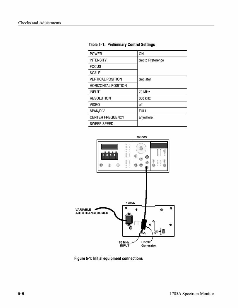
Checks and Adjustments
5- 6 1705A Spectrum Monitor
Table 5- 1: Preliminary Control Settings
POWER ON
INTENSITY Set to Preference
FOCUS
SCALE
VERTICAL POSITION Set later
HORIZONTAL POSITION
INPUT 70 MHz
RESOLUTION 300 kHz
VIDEO off
SPAN/DIV FULL
CENTER FREQUENCY anywhere
SWEEP SPEED
y
! !
SG503
CombGenerator
VARIABLEAUTOTRANSFORMER
70 MHzINPUT
1705A
Figure 5-1: Initial equipment connections
Checks and Adjustments
1705A Spectrum Monitor 5- 7
c. Connect the leveled sine wave generator output to the comb generator.Connect the comb generator output to the 1705A rear-panel 70 MHzINPUT. See Figure 5-1.
2. Check Power Supply Operation
REQUIREMENT — Check ac input range, 90 -- 250 V.
a. Set the leveled sine wave generator Frequency to 5.0 MHz, theAmplitude Multiplier to X1, and the Amplitude to 4.0 (+16 dBm).
b. Adjust the controls for a usable display.
c. Vary the autotransformer from low-line to high-line voltage (90 - 132 Vfor 110 V, or 180 - 250 V for 220 V operation).
d. CHECK -- for stable operation over the prescribed voltage range. (Note:If the LNB POWER is on and in use, the requirement is derated to 100 --132 V or 200 -- 250 V.)
e. Return the autotransformer to the local nominal mains voltage.
3. Check LNB Power Supply
REQUIREMENT — +18 Vdc ±5%.
a. Connect DVM leads between the center conductor of the L--BANDINPUT connector and ground.
b. Turn on the LNB POWER switch.
c. CHECK -- that the rear-panel, LNB POWER LED is ON, and that theDVM reads +18 V ±0.9 V.
d. Temporarily (approximately 2 seconds) short the L--BAND INPUTconnector center conductor to ground.
e. CHECK -- that the red indicator lamp extinguishes and then comes backon when the short is removed.
f. Turn LNB POWER off.
CAUTION. The LNB POWER switch MUST be turned off for the rest of this
procedure to prevent damage to the generators used in later steps.
4. Check 70 MHz Linearity
REQUIREMENT — One marker per Division ±1 minor Division.
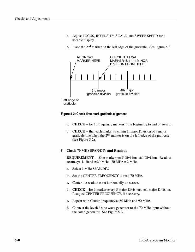
Checks and Adjustments
5- 8 1705A Spectrum Monitor
a. Adjust FOCUS, INTENSITY, SCALE, and SWEEP SPEED for auseable display.
b. Place the 2nd marker on the left edge of the graticule. See Figure 5-2.
ALIGN 2ndMARKER HERE
CHECK THAT 3rdMARKER IS +/-- 1 MINORDIVISION FROM HERE
Left edge ofgraticule
3rd majorgraticule division
4th majorgraticule division
Figure 5-2: Check time mark graticule alignment
c. CHECK -- for 10 frequency markers from beginning to end of sweep.
d. CHECK -- that each marker is within 1 minor Division of a majorgraticule line when the 2nd marker is on the left edge of the graticule(see Figure 5-2).
5. Check 70 MHz SPAN/DIV and Readout
REQUIREMENT — One marker per 5 Divisions ±1 Division. Readoutaccuracy: L--Band ±20 MHz. 70 MHz ±2 MHz.
a. Select 1 MHz SPAN/DIV.
b. Set the CENTER FREQUENCY to read 70 MHz.
c. Center the readout caret horizontally on screen.
d. CHECK -- for 1 marker every 5 major Divisions, ±1 major Division.Readjust CENTER FREQUENCY, if necessary.
e. Repeat with Center Frequency at 50 MHz and 90 MHz.
f. Connect the leveled sine wave generator to the 70 MHz input withoutthe comb generator. See Figure 5-3.
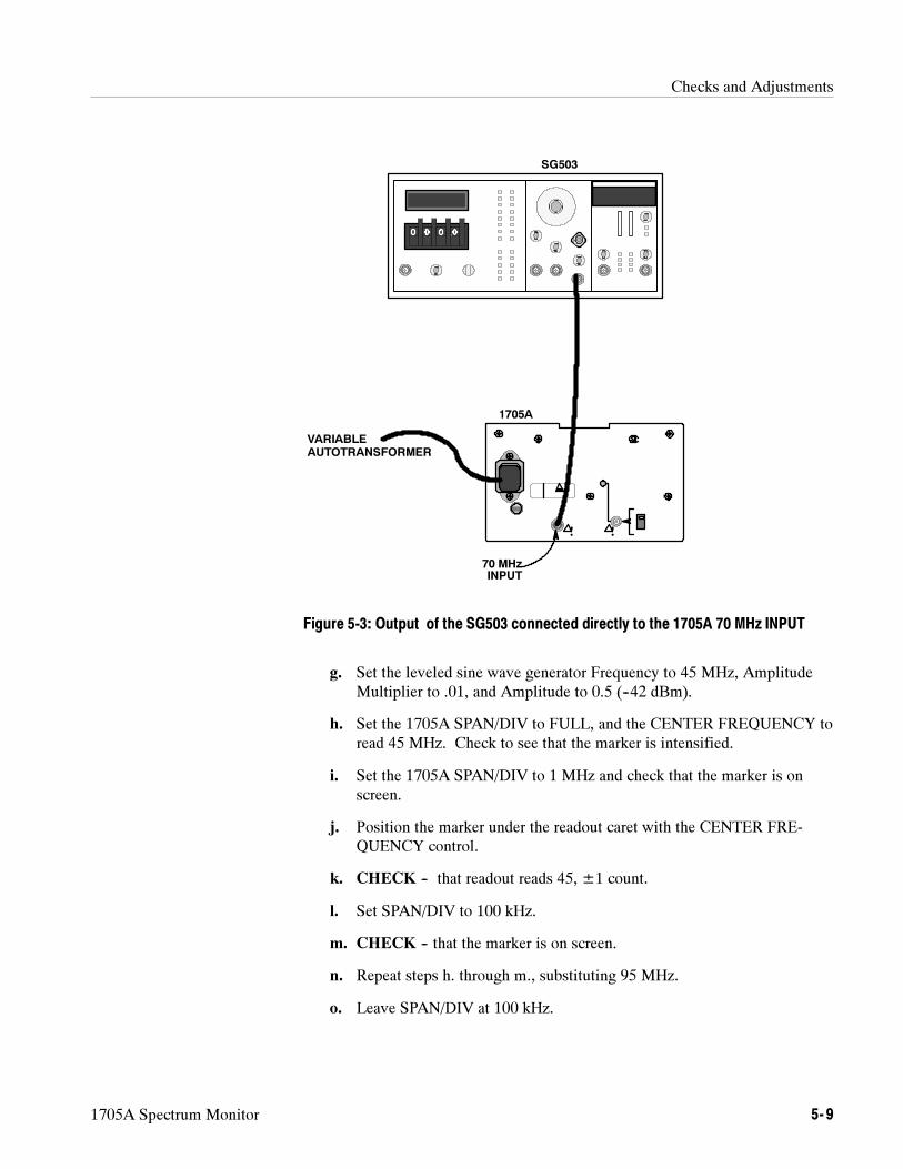
Checks and Adjustments
1705A Spectrum Monitor 5- 9
! !
SG503
VARIABLEAUTOTRANSFORMER
70 MHzINPUT
1705A
Figure 5-3: Output of the SG503 connected directly to the 1705A 70 MHz INPUT
g. Set the leveled sine wave generator Frequency to 45 MHz, AmplitudeMultiplier to .01, and Amplitude to 0.5 (--42 dBm).
h. Set the 1705A SPAN/DIV to FULL, and the CENTER FREQUENCY toread 45 MHz. Check to see that the marker is intensified.
i. Set the 1705A SPAN/DIV to 1 MHz and check that the marker is onscreen.
j. Position the marker under the readout caret with the CENTER FRE-QUENCY control.
k. CHECK -- that readout reads 45, ±1 count.
l. Set SPAN/DIV to 100 kHz.
m. CHECK -- that the marker is on screen.
n. Repeat steps h. through m., substituting 95 MHz.
o. Leave SPAN/DIV at 100 kHz.
Checks and Adjustments
5- 10 1705A Spectrum Monitor
6. Check Resolution Filter
REQUIREMENT -- 300 kHz Filter Resolution 200 -- 400 kHz. 10 kHzFilter Resolution 20 kHz or less. Filter through gain matches ±2 dB.
a. Adjust the leveled sine wave generator Amplitude for a 5 Division signalamplitude.
b. CHECK -- that the marker width 0.6 Divisions down from the top of thesignal is 3 Divisions, ±1 Division.
c. Change resolution to 10 kHz.
d. Set SWEEP SPEED fully counterclockwise.
e. CHECK -- that the marker width 0.6 Divisions down from the top of thesignal is ≤2 minor Divisions.
f. CHECK -- that the 10 kHz marker amplitude matches the highest pointof the 300 kHz marker amplitude within 1 minor Division, whenswitching between 300 KHZ and 10 KHZ RESOLUTION.
7. Check 70 MHz Gain and Flatness
REQUIREMENT -- Incremental Amplitude Accuracy ±4 dB/70 MHz.Flatness ±1 minor Division from 70 MHz to either 50 or 90 MHz.
a. Set SPAN/DIV to FULL.
b. Set RESOLUTION to 300 kHz.
c. Set SWEEP SPEED fully clockwise.
d. Set the leveled sine wave generator Frequency to 70 MHz, the Ampli-tude Multiplier to X1, and the Amplitude to 0.5 (--2 dBm).
e. CHECK -- for a marker amplitude change of 2 Divisions, ±2 minorDivisions when switching the leveled sine wave generator AmplitudeMultiplier between 0.01 and 0.1 (a 20 dB change).
f. Set the leveled sine wave generator Amplitude Multiplier to 0.01 andAmplitude to 0.5 (--42 dBm).
g. Position the tip of the marker to exact crt center with the HORIZONTALand VERTICAL POSITION controls.
h. Set the leveled sine wave generator Frequency to 50 MHz.
i. CHECK -- that the tip of the marker is on the crt center line, ±1 minorDivision (vertically).
j. Set the leveled sine wave generator Frequency to 90 MHz.
Checks and Adjustments
1705A Spectrum Monitor 5- 11
k. CHECK -- that the marker tip is on the crt center line±1 minorDivision (vertically).
8. Check Video Filter
REQUIREMENT -- Video Filter reduces noise by approximately 50%.
a. Be sure that the VIDEO FILTER is OFF.
b. Position the baseline on screen with the VERTICAL POSITION control.
c. Switch between VIDEO FILTER ON and OFF.
d. CHECK -- that the baseline noise amplitude drops approximately 50%when the VIDEO FILTER is ON.
9. Check Sweep Speed
REQUIREMENT -- Typically 20 -- 200 ms.
a. Verify that SPAN/DIV is set to FULL and that SWEEP SPEED is setfully clockwise.
b. CHECK -- for a solid trace with almost no flicker.
c. Set SWEEP SPEED fully counterclockwise.
d. CHECK -- for about 3 to 4 sweeps per second.
e. Return SWEEP SPEED fully clockwise.
Alternate Method
a. Connect the oscilloscope 10X probe to W2.
b. Set the oscilloscope timebase to 5 ms/Div.
c. Set the oscilloscope vertical to 2 Volts/Div.
d. Set SWEEP SPEED fully clockwise.
e. CHECK -- for a ramp duration of 20 ms ±10 ms.
f. Set SWEEP SPEED fully counterclockwise.
g. Set the oscilloscope timebase to 50 ms/Div.
h. CHECK -- for a ramp duration of 200 ms ±100 ms.
i. Remove probe. Return SWEEP SPEED fully clockwise.
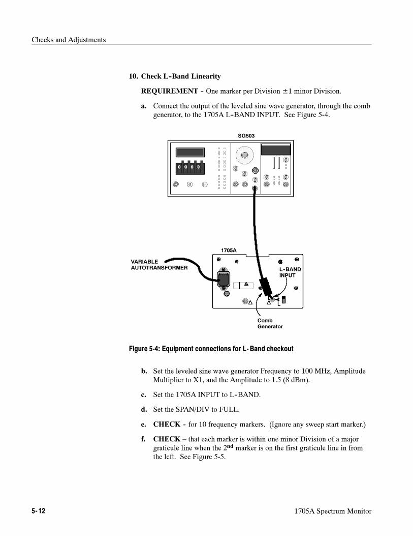
Checks and Adjustments
5- 12 1705A Spectrum Monitor
10. Check L--Band Linearity
REQUIREMENT -- One marker per Division ±1 minor Division.
a. Connect the output of the leveled sine wave generator, through the combgenerator, to the 1705A L--BAND INPUT. See Figure 5-4.
SG503
CombGenerator
VARIABLEAUTOTRANSFORMER L--BAND
INPUT
1705A
Figure 5-4: Equipment connections for L-Band checkout
b. Set the leveled sine wave generator Frequency to 100 MHz, AmplitudeMultiplier to X1, and the Amplitude to 1.5 (8 dBm).
c. Set the 1705A INPUT to L--BAND.
d. Set the SPAN/DIV to FULL.
e. CHECK -- for 10 frequency markers. (Ignore any sweep start marker.)
f. CHECK – that each marker is within one minor Division of a majorgraticule line when the 2nd marker is on the first graticule line in fromthe left. See Figure 5-5.
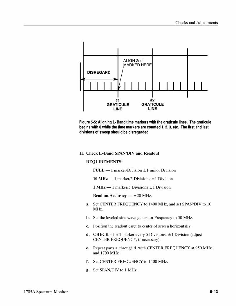
Checks and Adjustments
1705A Spectrum Monitor 5- 13
ALIGN 2ndMARKER HERE
DISREGARD
#1GRATICULE
LINE
#2GRATICULE
LINE
Figure 5-5: Aligning L-Band time markers with the graticule lines. The graticulebegins with 0 while the time markers are counted 1, 2, 3, etc. The first and lastdivisions of sweep should be disregarded
11. Check L--Band SPAN/DIV and Readout
REQUIREMENTS:
FULL — 1 marker/Division ±1 minor Division
10 MHz— 1 marker/5 Divisions ±1 Division
1 MHz— 1 marker/5 Divisions ±1 Division
Readout Accuracy — ±20 MHz.
a. Set CENTER FREQUENCY to 1400 MHz, and set SPAN/DIV to 10MHz.
b. Set the leveled sine wave generator Frequency to 50 MHz.
c. Position the readout caret to center of screen horizontally.
d. CHECK -- for 1 marker every 5 Divisions, ±1 Division (adjustCENTER FREQUENCY, if necessary).
e. Repeat parts a. through d. with CENTER FREQUENCY at 950 MHzand 1700 MHz.
f. Set CENTER FREQUENCY to 1400 MHz.
g. Set SPAN/DIV to 1 MHz.
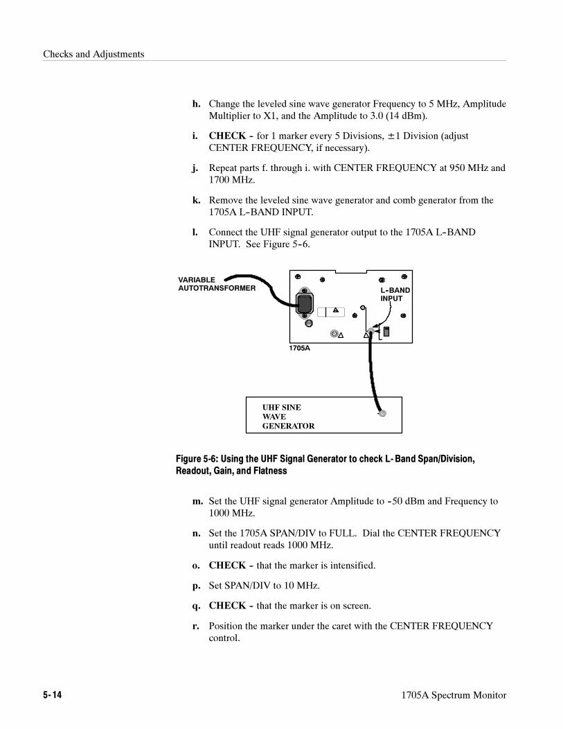
Checks and Adjustments
5- 14 1705A Spectrum Monitor
h. Change the leveled sine wave generator Frequency to 5 MHz, AmplitudeMultiplier to X1, and the Amplitude to 3.0 (14 dBm).
i. CHECK -- for 1 marker every 5 Divisions, ±1 Division (adjustCENTER FREQUENCY, if necessary).
j. Repeat parts f. through i. with CENTER FREQUENCY at 950 MHz and1700 MHz.
k. Remove the leveled sine wave generator and comb generator from the1705A L--BAND INPUT.
l. Connect the UHF signal generator output to the 1705A L--BANDINPUT. See Figure 5--6.
VARIABLEAUTOTRANSFORMER L--BAND
INPUT
UHF SINE
WAVE
GENERATOR
1705A
Figure 5-6: Using the UHF Signal Generator to check L-Band Span/Division,Readout, Gain, and Flatness
m. Set the UHF signal generator Amplitude to --50 dBm and Frequency to1000 MHz.
n. Set the 1705A SPAN/DIV to FULL. Dial the CENTER FREQUENCYuntil readout reads 1000 MHz.
o. CHECK -- that the marker is intensified.
p. Set SPAN/DIV to 10 MHz.
q. CHECK -- that the marker is on screen.
r. Position the marker under the caret with the CENTER FREQUENCYcontrol.
Checks and Adjustments
1705A Spectrum Monitor 5- 15
s. CHECK -- that the readout still reads 1000, ±10.
t. Set SPAN/DIV to 1 MHz.
u. CHECK -- that the marker is on screen. Position the marker under thecaret with the CENTER FREQUENCY control.
v. CHECK -- that the readout still reads 1000, ±10.
w. Set SPAN/DIV to 100 kHz.
x. CHECK -- that the marker is on screen.
y. Repeat steps m. through x., substituting 1700 MHz.
12. Check L--Band Gain and Flatness
REQUIREMENT -- Flatness: ±5 dB (± from center (1400 MHz)).Relative Amplitude Accuracy ±3 dB/100 MHz. (Typically ±1 dB/100MHz.)
a. Set SPAN/DIV to FULL.
b. Set the 1705A SWEEP SPEED fully counterclockwise.
c. Set the UHF signal generator Frequency to 1400 MHz and Amplitude to--30 dBm. Position the tip of the marker to the --10 graticule referenceline (vertical scale).
d. Change the UHF signal generator Frequency to 950 MHz.
e. CHECK -- that the marker is on the same crt center line (vertically),±0.5 Division.
f. Change the UHF signal generator Frequency to 1700 MHz.
g. CHECK -- that the marker is on the same crt line (vertically), ±0.5Division.
h. Set the UHF signal generator Frequency to 1400 MHz.
i. Position tip of marker to crt center.
j. CHECK -- that the marker tip is on the --10 graticule reference line,±0.5 Division. Note: Make sure that the baseline is on the --70graticule reference line.
13. Check Positioning Range
REQUIREMENT -- Vertical: + and --3 Divisions, Horizontal: + and --2Divisions.
Checks and Adjustments
5- 16 1705A Spectrum Monitor
a. Set the UHF signal generator Frequency to 1400 MHz, and Amplitude to--60 dBm.
b. CHECK -- that the tip can be positioned 2 Divisions left and right ofcenter.
c. Set the UHF signal generator Amplitude to --30 dBm.
d. Position baseline on the --60 graticule reference line.
e. CHECK -- that the marker tip can be positioned 3 Divisions down fromits present position.
f. CHECK -- that the baseline can be positioned to the --30 graticule line.
14. Check 2 dB/DIV Gain
REQUIREMENT -- Greater than 1 Division of amplitude change whilechanging from --50 dBm to --53 dBm.
a. Set the UHF signal generator Frequency to 1400 MHz, and Amplitude to--50 dBm.
b. Hold the VIDEO push button until 2 dB/Div appears on the crt readout.
c. Use the CENTER FREQUENCY control to locate the 1400 MHzmarker.
d. Select 100 kHz SPAN/DIV. Using CENTER FREQUENCY andVERTICAL controls, check that the marker tip can be positioned onscreen.
e. Return to FULL SPAN.
f. Turn the 1705A SWEEP SPEED control fully counterclockwise.
g. CHECK -- for more than 1 Division of amplitude change whileswitching the frequency generator between --50 dBm and --53 dBm.
h. CHECK -- that the noise floor can be positioned on screen.
i. Hold the VIDEO push button down again to exit the 2 dB/Div mode.
End of the Performance Check Procedure
Checks and Adjustments
1705A Spectrum Monitor 5- 17
Adjustment Procedure
The Adjustment Procedure covers only adjustments. Checks, other than thosethat must be made to ensure a step is completed, are in the Performance CheckProcedure.
There are actually two Adjustment Procedures, the short-form version isprovided for those familiar with the adjustments, while the longer (moredetailed) procedure is provided for those who need it.
Allow 20 minutes of warm-up time, at normal room temperature (approximately25° C) before making any adjustments to the instrument.
The Short-Form Adjustment Procedure has the adjustment steps in the sameorder as the longer form of the procedure, so the Short-Form Procedure can beused as an index for the Long Form. Circuit numbers for parts adjusted in thestep are also included with the step title.
A1 POWER SUPPLY BOARD
1. Adjust +5 V (R99)
2. Adjust CRT Bias (R58)
3. Adjust Geometry (R45), Center Focus (R11) and Astigmatism (R49)
4. Adjust Trace Rotation
A3 MAIN BOARD
5. Adjust On-Board Regulated Power Supplies (R99, --11.8V; R111, +11.8V)
6. Adjust Horizontal Gain (R168)
7. Adjust Readout Position (R27, Horizontal; R29, Vertical)
8. Adjust 360/119.8 MHz L.O. (C55, C69, L4, FL1, and FL2)
9. Adjust Ramp Size (R113)
10. Adjust 70 MHz Band Linearity (R55, R49, R56, R48, and R57)
11. Adjust 10 kHz Filter (C52, C62, C64, and R175)
12. Adjust L-Band Linearity (R35, R51, R58, R75, R81, and R82)
13. Adjust Readout Range (R4)
14. Adjust Span/Div Magnification Registration (R27)
Short- Form Procedure
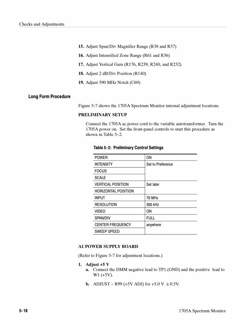
Checks and Adjustments
5- 18 1705A Spectrum Monitor
15. Adjust Span/Div Magnifier Range (R38 and R37)
16. Adjust Intensified Zone Range (R61 and R36)
17. Adjust Vertical Gain (R176, R239, R240, and R232)
18. Adjust 2 dB/Div Position (R140)
19. Adjust 590 MHz Notch (C69)
Figure 5-7 shows the 1705A Spectrum Monitor internal adjustment locations.
PRELIMINARY SETUP
Connect the 1705A ac power cord to the variable autotransformer. Turn the1705A power on. Set the front-panel controls to start this procedure asshown in Table 5--2.
Table 5- 2: Preliminary Control Settings
POWER ON
INTENSITY Set to Preference
FOCUS
SCALE
VERTICAL POSITION Set later
HORIZONTAL POSITION
INPUT 70 MHz
RESOLUTION 300 kHz
VIDEO ON
SPAN/DIV FULL
CENTER FREQUENCY anywhere
SWEEP SPEED
y
A1 POWER SUPPLY BOARD
(Refer to Figure 5-7 for adjustment locations.)
1. Adjust +5 Va. Connect the DMM negative lead to TP1 (GND) and the positive lead to
W1 (+5V).
b. ADJUST -- R99 (+5V ADJ) for +5.0 V 0.5V.
Long Form Procedure
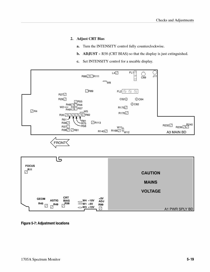
Checks and Adjustments
1705A Spectrum Monitor 5- 19
2. Adjust CRT Bias
a. Turn the INTENSITY control fully counterclockwise.
b. ADJUST -- R58 (CRT BIAS) so that the display is just extinguished.
c. Set INTENSITY control for a useable display.
CAUTION
MAINS
VOLTAGE
A1 PWR SPLY BD
R11
R45 R49 R58 W1 +5V
CRTBIASASTIG
GEOM
FOCUS
W4 --15V
W3 +15V
A3 MAIN BD
FRONT
R99 R111
L4 FL1
C69J11
FL2
C52 C64
C62
R175
R176
R232R239
R240
W12
W11
R168R140
R113
R89
W8
R27
R29R55
R56
R57W5
W2R48
R49R4
R36
R37
R38 R61
R35 R82
R51
R58R75R81
+5VADJ
R99
Figure 5-7: Adjustment locations
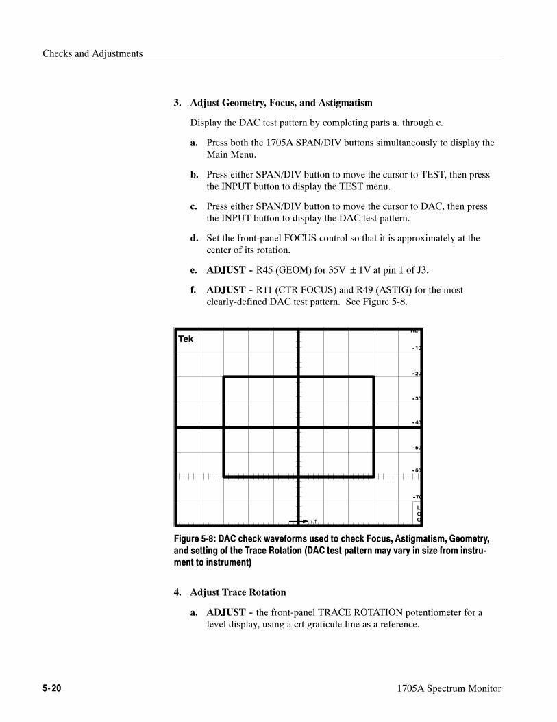
Checks and Adjustments
5- 20 1705A Spectrum Monitor
3. Adjust Geometry, Focus, and Astigmatism
Display the DAC test pattern by completing parts a. through c.
a. Press both the 1705A SPAN/DIV buttons simultaneously to display theMain Menu.
b. Press either SPAN/DIV button to move the cursor to TEST, then pressthe INPUT button to display the TEST menu.
c. Press either SPAN/DIV button to move the cursor to DAC, then pressthe INPUT button to display the DAC test pattern.
d. Set the front-panel FOCUS control so that it is approximately at thecenter of its rotation.
e. ADJUST -- R45 (GEOM) for 35V 1V at pin 1 of J3.
f. ADJUST -- R11 (CTR FOCUS) and R49 (ASTIG) for the mostclearly-defined DAC test pattern. See Figure 5-8.
TekREF
--10
--20
--30
--40
--50
--60
--70
L
O
G+ f
Figure 5-8: DAC check waveforms used to check Focus, Astigmatism, Geometry,and setting of the Trace Rotation (DAC test pattern may vary in size from instru-ment to instrument)
4. Adjust Trace Rotation
a. ADJUST -- the front-panel TRACE ROTATION potentiometer for alevel display, using a crt graticule line as a reference.
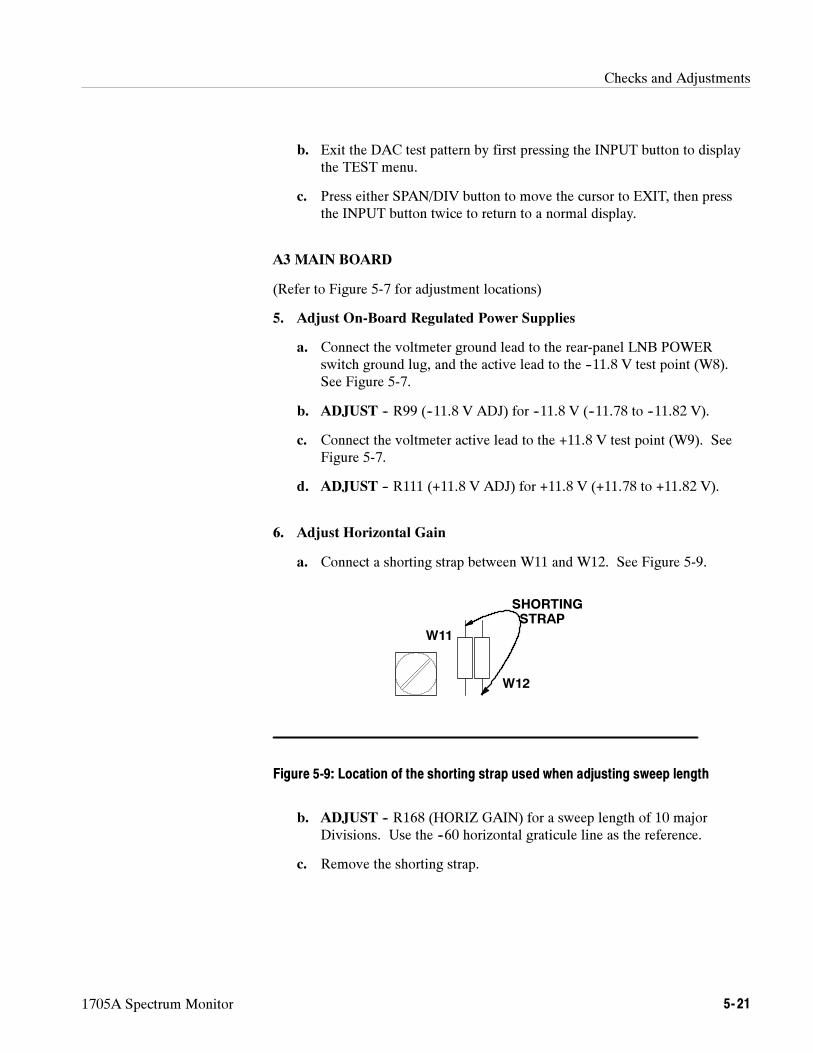
Checks and Adjustments
1705A Spectrum Monitor 5- 21
b. Exit the DAC test pattern by first pressing the INPUT button to displaythe TEST menu.
c. Press either SPAN/DIV button to move the cursor to EXIT, then pressthe INPUT button twice to return to a normal display.
A3 MAIN BOARD
(Refer to Figure 5-7 for adjustment locations)
5. Adjust On-Board Regulated Power Supplies
a. Connect the voltmeter ground lead to the rear-panel LNB POWERswitch ground lug, and the active lead to the --11.8 V test point (W8).See Figure 5-7.
b. ADJUST -- R99 (--11.8 V ADJ) for --11.8 V (--11.78 to --11.82 V).
c. Connect the voltmeter active lead to the +11.8 V test point (W9). SeeFigure 5-7.
d. ADJUST -- R111 (+11.8 V ADJ) for +11.8 V (+11.78 to +11.82 V).
6. Adjust Horizontal Gain
a. Connect a shorting strap between W11 and W12. See Figure 5-9.
W11
W12
SHORTINGSTRAP
Figure 5-9: Location of the shorting strap used when adjusting sweep length
b. ADJUST -- R168 (HORIZ GAIN) for a sweep length of 10 majorDivisions. Use the --60 horizontal graticule line as the reference.
c. Remove the shorting strap.
Checks and Adjustments
5- 22 1705A Spectrum Monitor
7. Adjust Readout Position
Display the DAC test pattern by completing parts a. through c.
a. Press both the 1705A SPAN/DIV buttons simultaneously to display theMain Menu.
b. Press either SPAN/DIV button to move the cursor to TEST, then pressthe INPUT button to display the TEST menu.
c. Press either SPAN/DIV button to move the cursor to DAC, then pressthe INPUT button to display the DAC test pattern.
d. ADJUST -- R27 and R29 (HORIZ and VERT POSN READOUT) for adisplay crossing at the crt center.
e. Exit the DAC test pattern by first pressing the INPUT button to displaythe TEST menu.
f. Press either SPAN/DIV button to move the cursor to EXIT, then pressthe INPUT button twice to return to a normal display.
8. Adjust 360/119.8 MHz L.O.
NOTE. Use an insulated tool for the following adjustments.
a. Adjust the VERTICAL POSITION control so that the crt trace is on the--70 graticule reference line.
b. Connect the signal generator to J11 (480 MHz IF Input). Set the outputFrequency for 489.7 MHz and the Amplitude to --40 dBm.
c. Select 300 kHz RESOLUTION.
d. Set C55 to full mesh, C69 to 1/8 mesh, and L4 to the top of the coil(three slug threads visible).
e. ADJUST -- FL1 for maximum signal (three screws beginning at theoutside adjustment screw). If no signal is present, adjust L4 down a fewturns and then adjust FL1.
f. ADJUST -- C55 for maximum signal. (C55 should peak at about 1/8 to1/2 mesh.)
g. ADJUST -- FL1, center and inside screws (do not readjust the outsidescrew), for maximum signal. (Less than one turn should be required.)
h. ADJUST -- FL2 for maximum signal (three screws beginning at the backscrew).
Checks and Adjustments
1705A Spectrum Monitor 5- 23
i. Repeat part i. using 2 dB/Div if necessary.
j. ADJUST -- C69 for maximum signal.
k. ADJUST -- L4 for maximum signal. (The slug may be removed if L4provides no benefit.)
l. Repeat this step as necessary until the signal amplitude is 37 to 43 dBabove the noise floor.
9. Adjust Ramp Size
a. On the 1705A select 70 MHz INPUT, turn the CENTER FREQUENCYknob fully counterclockwise, and set the SPAN/DIV to 1 MHz.
b. Set the DVM to AC Volts.
c. Connect the ground lead to chassis ground and the active lead to W5.See Figure 5-7.
d. Note reading on the DVM (should be¶0.4 volts).
e. Connect the DVM to W2. See Figure 5-7.
f. Set the 1705A SPAN/DIV to FULL.
g. ADJUST -- R113 (FULL GAIN) to match the reading from part d.
10. Adjust 70 MHz Band Linearity
a. Set SWEEP SPEED fully clockwise, SPAN/DIV to 1 MHz, and adjustthe HORIZONTAL POSITION to place the caret on the center graticule.
b. Set the SPAN/DIV to FULL.
c. Connect the signal generator output to the 1705A 70 MHz INPUT.
d. Set the signal generator Frequency to 45 MHz, and the Amplitude to--25 dBm.
e. ADJUST -- R55 to place the signal on the extreme left graticule.
NOTE. Ramp start amplitude (step 9) should be verified after R55 and 70 MHz
linearity are completed and the 70 MHz tuner cover is on. All of these adjust-
ments interact and ramp start amplitude is critical for proper linearity.
f. Connect the signal generator output to the 1705A 70 MHz INPUTthrough the comb generator.
Checks and Adjustments
5- 24 1705A Spectrum Monitor
g. Set the signal generator Frequency to 5.0 MHz, and the Amplitude to+10 dBm.
h. Position the first marker at the extreme left graticule.
i. ADJUST -- R49, R56, R48, then adjust R57 to position one marker permajor Division over the 10 major graticule Divisions, ±1 minorDivision. (All these adjustments affect dc level of ramp start in 70 MHztuner.)
11. Adjust 10 kHz Filter
a. Remove the comb generator and reconnect the cable from the signalgenerator to the 1705A 70 MHz INPUT.
b. Set the signal generator Frequency to 70 MHz, and the Amplitude to --25dBm.
c. On the 1705A set SPAN/DIV to 100 kHz, adjust CENTER FREQUEN-CY to position the marker onto the screen, and set RESOLUTION to 10kHz.
d. ADJUST -- C52, C62, and C64 for a tall, symmetrical signal (¶6Divisions).
e. Set RESOLUTION to 300 kHz, and turn SWEEP SPEED fullycounterclockwise.
f. ADJUST -- R175 to match the signal amplitude of the highest point ofthe 300 kHz filtered marker with the tip of the 10 kHz filtered markerwhile switching between 10 kHz and 300 kHz RESOLUTION.
12. Adjust L--Band Linearity
a. Set INPUT to L--BAND and SPAN/DIV to 10 MHz. Adjust theHORIZONTAL POSITION control to center the caret, and then setSPAN/DIV to FULL.
b. Connect the signal generator output to the L--BAND INPUT.
c. Set the signal generator Frequency to 900 MHz, and Amplitude to --30dBm.
d. ADJUST -- R35 to position the signal on the extreme left graticule.
e. Connect the signal generator output to the L--BAND INPUT through thecomb generator.
f. Set the signal generator Frequency to 100 MHz, and Amplitude to +10dBm.
Checks and Adjustments
1705A Spectrum Monitor 5- 25
g. ADJUST -- R51, R58, R75, R81, and R82 for a linear display with eachmarker on a graticule mark, ±1 minor Division.
h. Readjust R35 to place first marker on the extreme left graticule.
NOTE. Readjustment of R35 may cause a change in linearity.
13. Adjust Readout Range
a. Turn CENTER FREQUENCY fully counterclockwise.
b. ADJUST -- R4 (Readout Cal) so the frequency readout displays900 MHz.
14. Adjust Span/Div Magnification Registration
a. Set SPAN/DIV to 1 MHz.
b. Turn the CENTER FREQUENCY control to position any marker underthe readout caret.
c. Set SPAN/DIV to 10 MHz.
d. ADJUST -- R27 (Horiz Posn Readout) to position the caret directly overthe marker.
e. Set SPAN/DIV to 1 MHz. Marker should be under caret ±1 minorDivision.
f. Adjust the HORIZONTAL POSITION control to place the caret at thecenter of the screen.
g. If R27 requires adjustment, check step 10 parts a. through e. (R55), andcheck step 12 parts a. through d. (R35).
15. Adjust Span/Div Magnifier Range
a. Set SPAN/DIV to 10 MHz.
b. Use the HORIZONTAL POSITION control to position the caret to thecenter screen graticule line.
c. Turn the CENTER FREQUENCY control fully clockwise (the readoutshould display 2000 MHz±50 MHz).
d. Set the signal generator Frequency to 1800 MHz, and Amplitude to --30dBm.
Checks and Adjustments
5- 26 1705A Spectrum Monitor
e. Turn the CENTER FREQUENCY control counterclockwise until thefrequency readout display is 1800 MHz.
f. ADJUST -- R38 (Offset) to position the 1800 MHz marker directlyunder the caret.
g. Set the signal generator Frequency to 1000 MHz.
h. Turn the CENTER FREQUENCY control to display 1000 MHz.
i. ADJUST -- R37 (Offset Gain) to position the 1000 MHz marker directlyunder the caret.
j. Repeat this step until the markers at 1800 and 1000 MHz are properlypositioned.
16. Adjust Intensified Zone Range
a. Set the SPAN/DIV to FULL.
b. Set the signal generator Frequency to 1400 MHz, and Amplitude to --30dBm.
c. Adjust the CENTER FREQUENCY control so the readout displays 1400MHz.
d. ADJUST -- R61 to center the intensified zone on the 1400 MHz marker.
e. Set the leveled sine wave generator Frequency to 1000 MHz.
f. Turn the CENTER FREQUENCY control counterclockwise to 1000MHz.
g. ADJUST -- R36 to center the intensified zone on the 900 MHz marker.
h. Repeat this step until the intensified zone is centered on appropriatemarkers.
17. Adjust Vertical Gain
a. Set the 1705A SWEEP SPEED fully counterclockwise.
b. Set the signal generator Frequency to 1400 MHz, and Amplitude to--30 dBm.
c. ADJUST -- R176 for a three-Division shift (±0.25 major Divisions)when switching the input level between --30 and --60 dBm.
d. Set VERTICAL POSITION to place the noise floor one major Divisionup from the bottom graticule line.
Checks and Adjustments
1705A Spectrum Monitor 5- 27
e. ADJUST -- R239 (IF AGC) for maximum signal amplitude.
f. ADJUST -- R240 (RF AGC) so the signal is one major Division (±0.5major Divisions) down from the top graticule line.
g. ADJUST -- R232 to its midpoint.
18. Adjust 2 dB/Div Position
a. Disconnect the signal from the L--BAND INPUT.
b. Turn VERTICAL POSITION fully clockwise.
c. Hold the VIDEO push button down until 2 dB/Div appears on the crtreadout.
d. ADJUST -- R140 to position the noise floor to center screen.
e. Hold the VIDEO push button down again to exit the 2 dB/Div mode.
19. Adjust 590 MHz Notch
a. Select L--BAND INPUT and set the SPAN/DIV to 10 MHz.
b. Connect the signal generator to the L--BAND INPUT.
c. Set the signal generator Frequency to 1200 MHz, and Amplitude to--20 dBm.
d. Use the HORIZONTAL POSITION control to place the 1200 MHzsignal at the extreme left graticule mark. A small spur should be visiblenear the extreme right graticule mark. Note: R240, RF AGC, may beadjusted to ease visibility of the spur. Be sure to reset R240 (step 17part f.).
e. ADJUST -- C69 carefully until spur is minimized. Note: Whileadjusting C69, note the 1200 MHz amplitude. The spur should beminimized without reducing the 1200 MHz spike by more than 2 dB.
End of Adjustment Procedure

Checks and Adjustments
5- 28 1705A Spectrum Monitor

Maintenance

Test Equipment Depot - 800.517.8431 - 99 Washington Street Melrose, MA 02176 - FAX 781.665.0780 - TestEquipmentDepot.com
1705A Spectrum Monitor 6- 1
Section 6Maintenance
This section contains instructions for preventive maintenance, diagnostics,general troubleshooting, and corrective maintenance. If the instrument does notfunction properly, troubleshooting and corrective measures should be takenimmediately to circumvent additional problems.
PREVENTIVE MAINTENANCE
Preventive maintenance consists of cleaning, visual inspection, performancechecking, and, if needed, readjustment. The preventive maintenance scheduleestablished for the instrument should be based on the environment in which it isoperated and the amount of use. Under average conditions, scheduled preventivemaintenance should be performed every 2000 hours of operation.
CAUTION. A 2% RMA flux content solder is recommended for making repairs in
this instrument. Cleaning of rosin residue is not recommended. Most cleaning
solvents tend to reactivate the rosin and spread it under components where it
may cause corrosion under humid conditions. The rosin residue, if left alone,
does not exhibit these corrosive properties.
The instrument should be cleaned often enough to prevent dust or dirt fromaccumulating. Dirt acts as a thermal insulating blanket that prevents effectiveheat dissipation, and can provide high-resistance electrical leakage paths betweenconductors or components in a humid environment.
Exterior. Clean the dust from the outside of the instrument by wiping with asoft cloth or small brush. A brush is especially useful to remove dust fromaround the selector buttons, knobs, and connectors. Hardened dirt may beremoved with a cloth dampened in water that contains a mild detergent.Abrasive cleaners should not be used.
Crt. Clean the crt protective shield, light filter, and crt face with a soft, lint-freecloth dampened in denatured alcohol.
Interior. Clean the interior of the instrument by loosening the accumulated dustwith a dry, soft brush. Once the dirt is loosened remove it with low--pressure air(high-velocity air can damage some parts). Hardened dirt or grease may beremoved with a cotton-tipped applicator dampened with a solution of mild
Cleaning
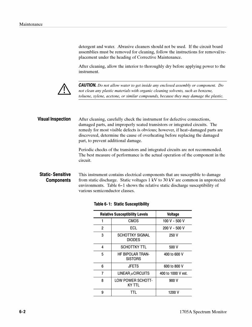
Maintenance
6- 2 1705A Spectrum Monitor
detergent and water. Abrasive cleaners should not be used. If the circuit boardassemblies must be removed for cleaning, follow the instructions for removal/re-placement under the heading of Corrective Maintenance.
After cleaning, allow the interior to thoroughly dry before applying power to theinstrument.
CAUTION. Do not allow water to get inside any enclosed assembly or component. Do
not clean any plastic materials with organic cleaning solvents, such as benzene,
toluene, xylene, acetone, or similar compounds, because they may damage the plastic.
After cleaning, carefully check the instrument for defective connections,damaged parts, and improperly seated transistors or integrated circuits. Theremedy for most visible defects is obvious; however, if heat--damaged parts arediscovered, determine the cause of overheating before replacing the damagedpart, to prevent additional damage.
Periodic checks of the transistors and integrated circuits are not recommended.The best measure of performance is the actual operation of the component in thecircuit.
This instrument contains electrical components that are susceptible to damagefrom static discharge. Static voltages 1 kV to 30 kV are common in unprotectedenvironments. Table 6--1 shows the relative static discharge susceptibility ofvarious semiconductor classes.
Table 6- 1: Static Susceptibility
Relative Susceptibility Levels Voltage
1 CMOS 100 V -- 500 V
2 ECL 200 V -- 500 V
3 SCHOTTKY SIGNALDIODES
250 V
4 SCHOTTKY TTL 500 V
5 HF BIPOLAR TRAN-SISTORS
400 to 600 V
6 JFETS 600 to 800 V
7 LINEAR CIRCUITS 400 to 1000 V est.
8 LOW POWER SCHOTT-KY TTL
900 V
9 TTL 1200 V
Visual Inspection
Static- SensitiveComponents
Maintenance
1705A Spectrum Monitor 6- 3
Observe the following precautions to avoid damage:
1. Minimize handling of static-sensitive components.
2. Transport and store static-sensitive components or assemblies in theiroriginal containers, on a metal rail, or on conductive foam. Label anypackage that contains static-sensitive components or assemblies.
3. Discharge the static voltage from your body, by wearing a wrist groundingstrap, while handling these components. Servicing static-sensitive assem-blies or components should be done only at a static-free work station byqualified personnel.
4. Nothing capable of generating or holding a static charge should be allowedon the work station surface.
5. Keep the component leads shorted together whenever possible.
6. Pick up the components by the body, never by the leads.
7. Do not slide the components over any surface.
8. Avoid handling components in areas that have a floor or work surfacecovering capable of generating a static charge.
9. Use a soldering iron that is connected to earth ground.
10. Use only special antistatic, suction, or wick-type desoldering tools.
Instrument performance should be checked after each 2000 hours of operation, orevery 12 months, if used intermittently. This will help to ensure maximumperformance and assist in locating defects that may not be apparent duringregular operation. The Performance Check Procedure and the AdjustmentProcedure are in Section 5.
TROUBLESHOOTING
The 1705A is equipped with a microprocessor and, as with all of the newTektronix monitors, it is capable of some power-up and off-line diagnostics. Athorough understanding of the information available in the diagnostic routineswill assist in isolating problems and speed repairs.
Performance Checks andReadjustments
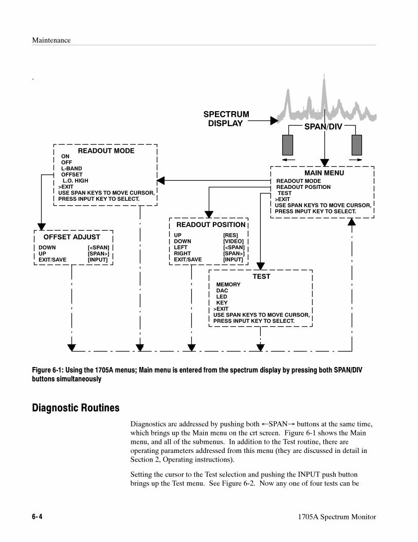
Maintenance
6- 4 1705A Spectrum Monitor
.
SPECTRUM
DISPLAY
READOUT MODEONOFFL-BANDOFFSETL.O. HIGH
>EXITUSE SPAN KEYS TO MOVE CURSOR,PRESS INPUT KEY TO SELECT.
MAIN MENUREADOUT MODEREADOUT POSITIONTEST
>EXITUSE SPAN KEYS TO MOVE CURSOR,PRESS INPUT KEY TO SELECT.
READOUT POSITION
OFFSET ADJUST
TESTMEMORYDACLEDKEY
>EXITUSE SPAN KEYS TO MOVE CURSOR,PRESS INPUT KEY TO SELECT.
DOWNUPEXIT/SAVE
[<SPAN][SPAN>][INPUT]
UPDOWNLEFTRIGHTEXIT/SAVE
[RES][VIDEO][<SPAN][SPAN>][INPUT]
SPAN/DIV
Figure 6-1: Using the 1705A menus; Main menu is entered from the spectrum display by pressing both SPAN/DIVbuttons simultaneously
Diagnostic Routines
Diagnostics are addressed by pushing both ←SPAN→ buttons at the same time,which brings up the Main menu on the crt screen. Figure 6-1 shows the Mainmenu, and all of the submenus. In addition to the Test routine, there areoperating parameters addressed from this menu (they are discussed in detail inSection 2, Operating instructions).
Setting the cursor to the Test selection and pushing the INPUT push buttonbrings up the Test menu. See Figure 6-2. Now any one of four tests can be
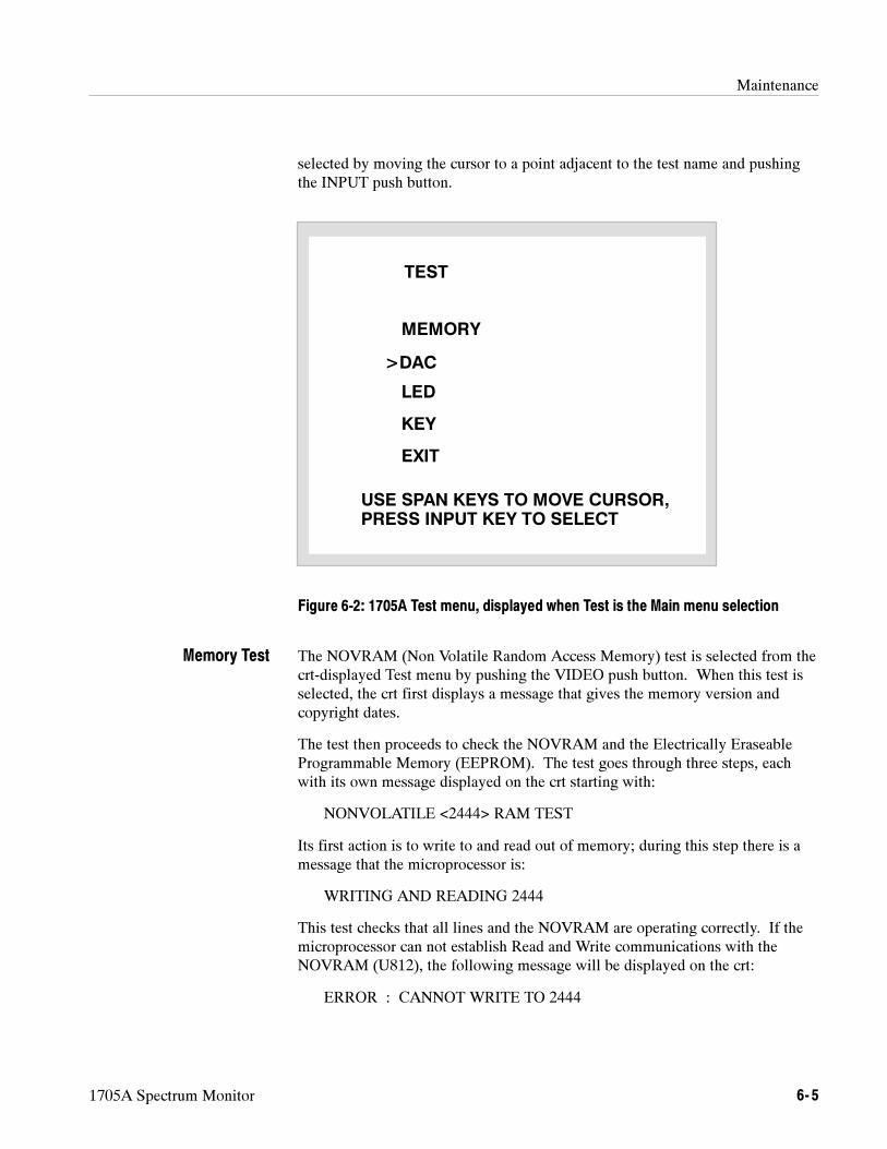
Maintenance
1705A Spectrum Monitor 6- 5
selected by moving the cursor to a point adjacent to the test name and pushingthe INPUT push button.
USE SPAN KEYS TO MOVE CURSOR,PRESS INPUT KEY TO SELECT
TEST
MEMORY
>DAC
LED
KEY
EXIT
Figure 6-2: 1705A Test menu, displayed when Test is the Main menu selection
The NOVRAM (Non Volatile Random Access Memory) test is selected from thecrt-displayed Test menu by pushing the VIDEO push button. When this test isselected, the crt first displays a message that gives the memory version andcopyright dates.
The test then proceeds to check the NOVRAM and the Electrically EraseableProgrammable Memory (EEPROM). The test goes through three steps, eachwith its own message displayed on the crt starting with:
NONVOLATILE <2444> RAM TEST
Its first action is to write to and read out of memory; during this step there is amessage that the microprocessor is:
WRITING AND READING 2444
This test checks that all lines and the NOVRAM are operating correctly. If themicroprocessor can not establish Read and Write communications with theNOVRAM (U812), the following message will be displayed on the crt:
ERROR : CANNOT WRITE TO 2444
Memory Test
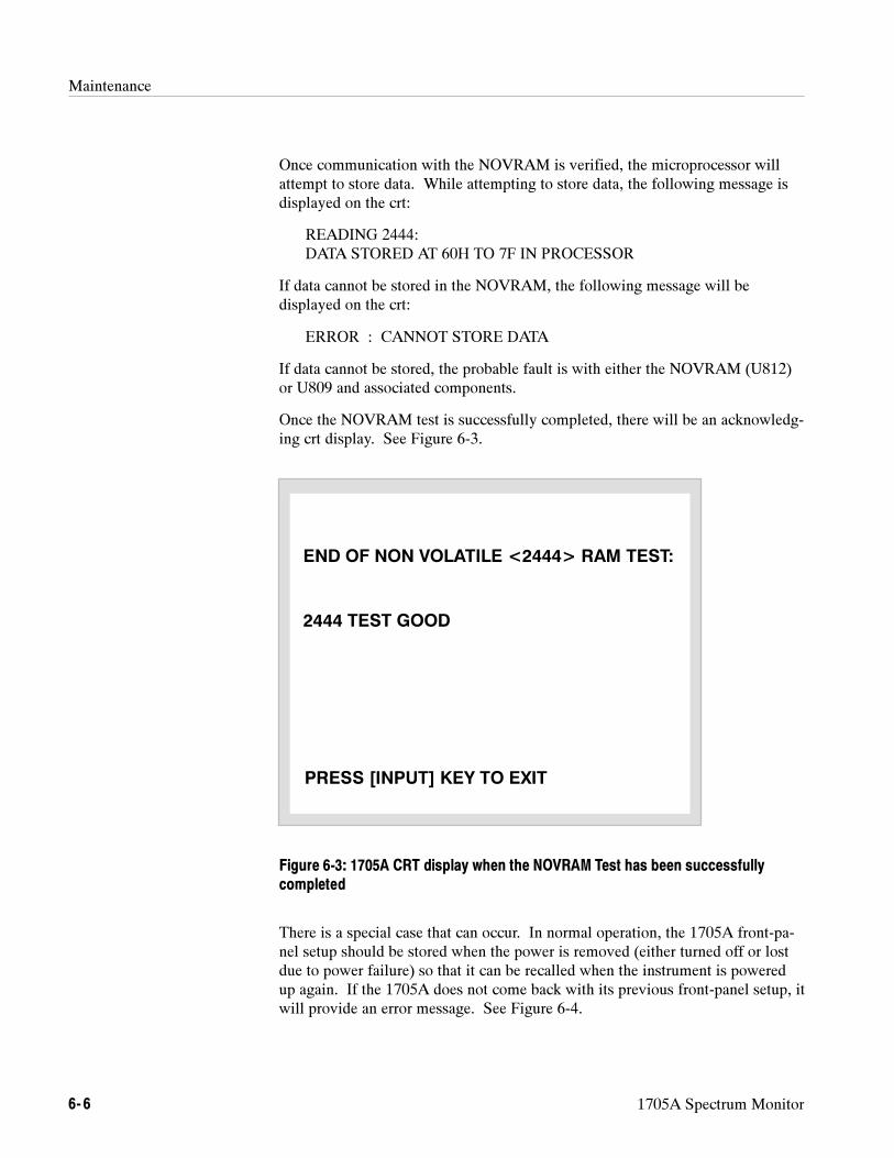
Maintenance
6- 6 1705A Spectrum Monitor
Once communication with the NOVRAM is verified, the microprocessor willattempt to store data. While attempting to store data, the following message isdisplayed on the crt:
READING 2444:DATA STORED AT 60H TO 7F IN PROCESSOR
If data cannot be stored in the NOVRAM, the following message will bedisplayed on the crt:
ERROR : CANNOT STORE DATA
If data cannot be stored, the probable fault is with either the NOVRAM (U812)or U809 and associated components.
Once the NOVRAM test is successfully completed, there will be an acknowledg-ing crt display. See Figure 6-3.
END OF NON VOLATILE <2444> RAM TEST:
2444 TEST GOOD
PRESS [INPUT] KEY TO EXIT
Figure 6-3: 1705A CRT display when the NOVRAM Test has been successfullycompleted
There is a special case that can occur. In normal operation, the 1705A front-pa-nel setup should be stored when the power is removed (either turned off or lostdue to power failure) so that it can be recalled when the instrument is poweredup again. If the 1705A does not come back with its previous front-panel setup, itwill provide an error message. See Figure 6-4.
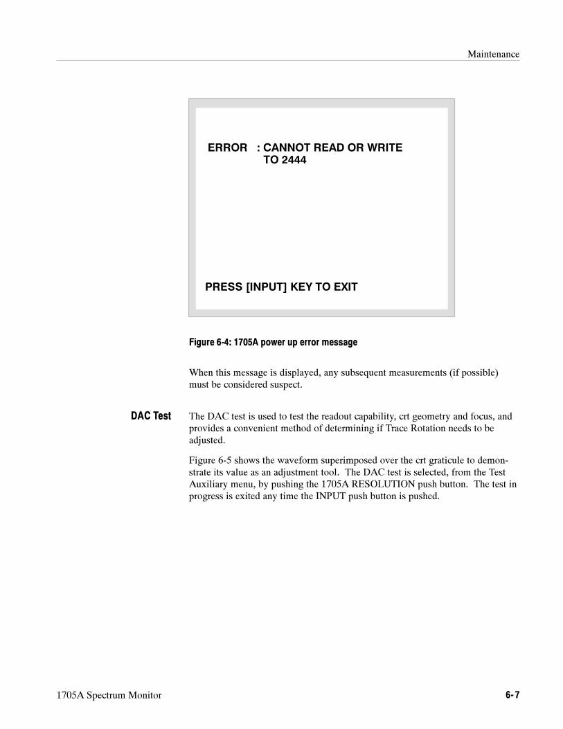
Maintenance
1705A Spectrum Monitor 6- 7
PRESS [INPUT] KEY TO EXIT
ERROR : CANNOT READ OR WRITETO 2444
Figure 6-4: 1705A power up error message
When this message is displayed, any subsequent measurements (if possible)must be considered suspect.
The DAC test is used to test the readout capability, crt geometry and focus, andprovides a convenient method of determining if Trace Rotation needs to beadjusted.
Figure 6-5 shows the waveform superimposed over the crt graticule to demon-strate its value as an adjustment tool. The DAC test is selected, from the TestAuxiliary menu, by pushing the 1705A RESOLUTION push button. The test inprogress is exited any time the INPUT push button is pushed.
DAC Test
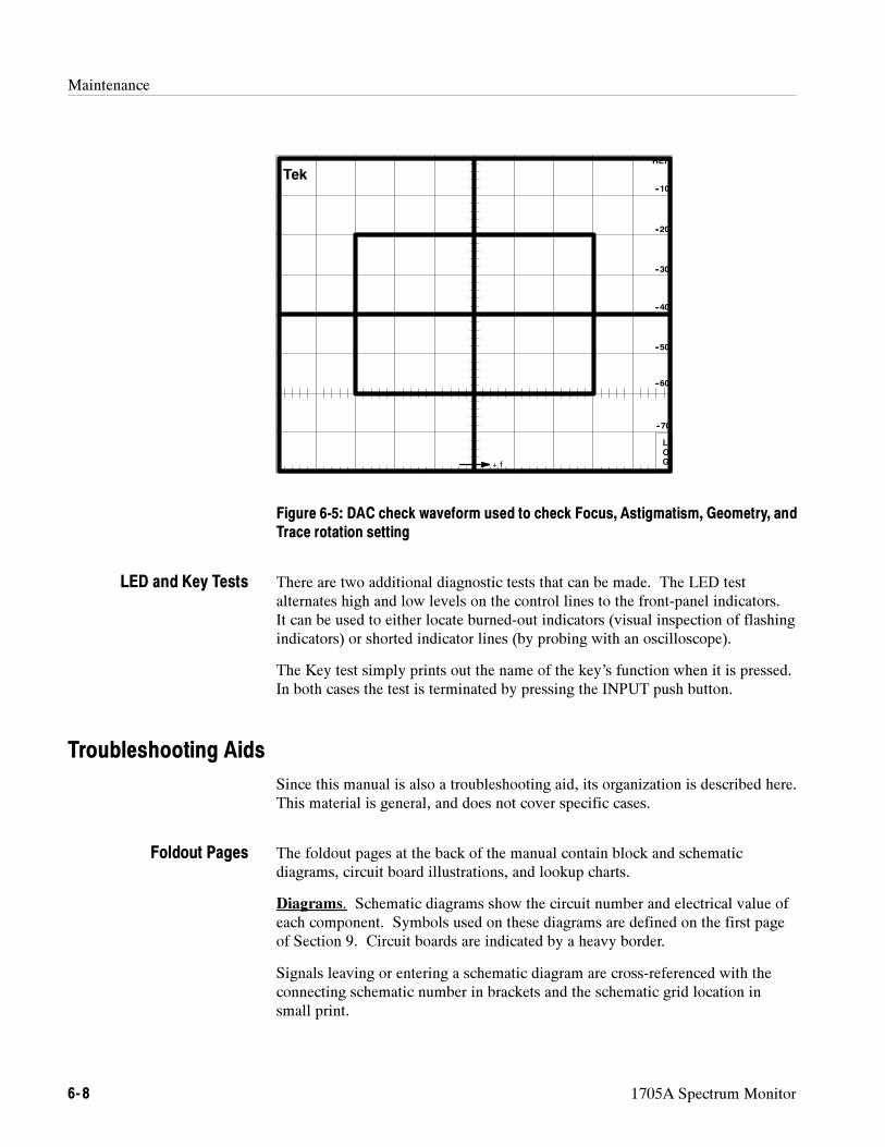
Maintenance
6- 8 1705A Spectrum Monitor
TekREF
--10
--20
--30
--40
--50
--60
--70
L
O
G+ f
Figure 6-5: DAC check waveform used to check Focus, Astigmatism, Geometry, andTrace rotation setting
There are two additional diagnostic tests that can be made. The LED testalternates high and low levels on the control lines to the front-panel indicators.It can be used to either locate burned-out indicators (visual inspection of flashingindicators) or shorted indicator lines (by probing with an oscilloscope).
The Key test simply prints out the name of the key’s function when it is pressed.In both cases the test is terminated by pressing the INPUT push button.
Troubleshooting Aids
Since this manual is also a troubleshooting aid, its organization is described here.This material is general, and does not cover specific cases.
The foldout pages at the back of the manual contain block and schematicdiagrams, circuit board illustrations, and lookup charts.
Diagrams. Schematic diagrams show the circuit number and electrical value ofeach component. Symbols used on these diagrams are defined on the first pageof Section 9. Circuit boards are indicated by a heavy border.
Signals leaving or entering a schematic diagram are cross-referenced with theconnecting schematic number in brackets and the schematic grid location insmall print.
LED and Key Tests
Foldout Pages
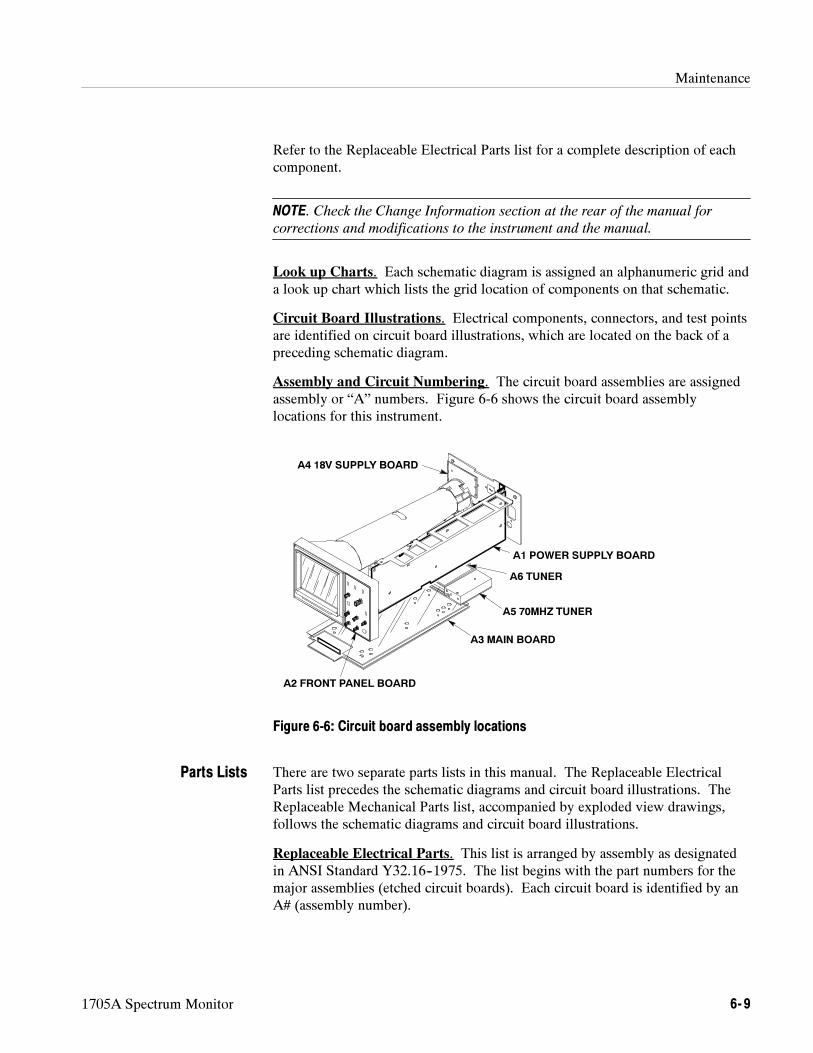
Maintenance
1705A Spectrum Monitor 6- 9
Refer to the Replaceable Electrical Parts list for a complete description of eachcomponent.
NOTE. Check the Change Information section at the rear of the manual for
corrections and modifications to the instrument and the manual.
Look up Charts. Each schematic diagram is assigned an alphanumeric grid anda look up chart which lists the grid location of components on that schematic.
Circuit Board Illustrations. Electrical components, connectors, and test pointsare identified on circuit board illustrations, which are located on the back of apreceding schematic diagram.
Assembly and Circuit Numbering. The circuit board assemblies are assignedassembly or “A” numbers. Figure 6-6 shows the circuit board assemblylocations for this instrument.
A2 FRONT PANEL BOARD
A3 MAIN BOARD
A1 POWER SUPPLY BOARD
A4 18V SUPPLY BOARD
A5 70MHZ TUNER
A6 TUNER
Figure 6-6: Circuit board assembly locations
There are two separate parts lists in this manual. The Replaceable ElectricalParts list precedes the schematic diagrams and circuit board illustrations. TheReplaceable Mechanical Parts list, accompanied by exploded view drawings,follows the schematic diagrams and circuit board illustrations.
Replaceable Electrical Parts. This list is arranged by assembly as designatedin ANSI Standard Y32.16--1975. The list begins with the part numbers for themajor assemblies (etched circuit boards). Each circuit board is identified by anA# (assembly number).
Parts Lists

Maintenance
6- 10 1705A Spectrum Monitor
The circuit numbers of the individual components in the parts list is made up bycombining the assembly number with the individual circuit number. EXAM-PLE: R117 on Assembly (circuit board) A3 is listed in the ReplaceableElectrical Parts list as A3R117.
NOTE. Always consult the parts list and “Change Information” for part numbers
and descriptions before ordering replacement parts. Some parts may have been
replaced in an individual instrument.
Replaceable Mechanical Parts. Parts listed in the Replaceable MechanicalParts list are assigned index numbers which correspond to circled numbers onthe exploded view drawing(s).
Accessories List. Standard accessories are illustrated in the exploded viewdrawing. Part numbers of standard and optional accessories are given at the endof the Replaceable Mechanical Parts list.
Signals and power supply voltages are passed through the instrument with asystem of interconnecting cables. The connector holders on these cables havenumbers that identify terminal connectors; numerals are used from 2 up. Atriangular key symbol is used to identify pin 1 on the circuit board and theconnector to assist in aligning the connector with correct square pins. Figure 6-7shows the numbering scheme (and the triangular marking) on the connector andthe marking on the etched circuit board.
A pin replacement kit including necessary tools, instructions, and replacementpins is available from Tektronix, Inc. Contact a Tektronix field office orrepresentative for assistance in ordering this kit.
Connectors with Center Polarizers. These polarizers serve as a key for propermating with the connector on the circuit board. Pin 1 is also marked with atriangular symbol on both connectors.
The following procedure is designed to assist in isolating problems, which inturn expedites repairs and minimizes down time.
1. Ensure that the malfunction exists in the instrument. This is done by makingsure that the instrument is operating as intended by Tektronix (see OperatingInstructions in Section 2).
2. Determine the nature of the problem. Attempt to make the determination ofwhether the instrument is out of calibration or if there has been a componentfailure. Once the type of failure has been determined, proceed on to identifythe functional area most likely at fault.
Major AssemblyInterconnection
General TroubleshootingTechniques
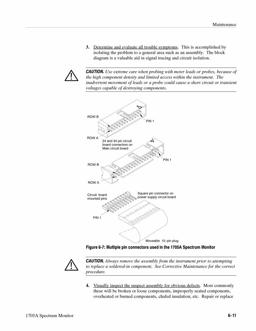
Maintenance
1705A Spectrum Monitor 6- 11
3. Determine and evaluate all trouble symptoms. This is accomplished byisolating the problem to a general area such as an assembly. The blockdiagram is a valuable aid in signal tracing and circuit isolation.
CAUTION. Use extreme care when probing with meter leads or probes, because of
the high component density and limited access within the instrument. The
inadvertent movement of leads or a probe could cause a short circuit or transient
voltages capable of destroying components.
Circuit boardmounted pins
PIN 1
Moveable 10--pin plug
Square pin connector onpower supply circuit board
PIN 1
PIN 1
24 and 34 pin circuitboard connectors onMain circuit board
ROW A
ROW B
ROW B
ROW A
Figure 6-7: Multiple pin connectors used in the 1705A Spectrum Monitor
CAUTION. Always remove the assembly from the instrument prior to attempting
to replace a soldered-in component. See Corrective Maintenance for the correct
procedure.
4. Visually inspect the suspect assembly for obvious defects. Most commonlythese will be broken or loose components, improperly seated components,overheated or burned components, chafed insulation, etc. Repair or replace
Maintenance
6- 12 1705A Spectrum Monitor
all obvious defects. In the case of overheated components, determine andcorrect the cause of overheating before re-applying power.
5. Use successive electrical checks to locate the source of the problem. Theprimary tool for problem isolation is the oscilloscope. Use the PerformanceCheck Procedure (located in Section 5) to determine if a circuit is operatingwithin specifications. At times it may be necessary to change a calibrationadjustment to determine if a circuit is operational, but since this can destroyinstrument calibration, care should be exercised. Before changing anadjustment, note its position so that it can be returned to its original setting.
6. Determine the extent of the repair. If the necessary repair is complex, it maybe advisable to contact your local Tektronix field office or representativebefore continuing. If the repair is minor, such as replacing a component, seethe parts list for replacement information. Removal and replacementprocedures for the assemblies can be found under Corrective Maintenance.
Power Supply Troubleshooting Procedure
NOTE. A review of the power supply theory of operation is recommended before
attempting repairs.
The equipment needed to troubleshoot the power supply:
Digital Multimeter (DMM), with a diode check function
Oscilloscope
0 to 20 Vdc Variable Power Supply
Clip Lead -- to short across a component
High Voltage Probe, ≥1 GΩ input resistance
The Troubleshooting Procedure for the Power Supply (Assembly A1) is split intotwo sections, the Low Volts and High Volts Supplies. Start the procedure bydetermining which section of the Power Supply the problem is in. Apply acpower and turn on the Power Supply. From Table 6--2, determine whichsymptom the Power Supply exhibits and refer to the corresponding procedure.
Table 6- 2: Power Supply Fault Symptoms
Symptom Procedure
Line fuse open Rectifier/Switcher Check (Low Volts)
Introduction
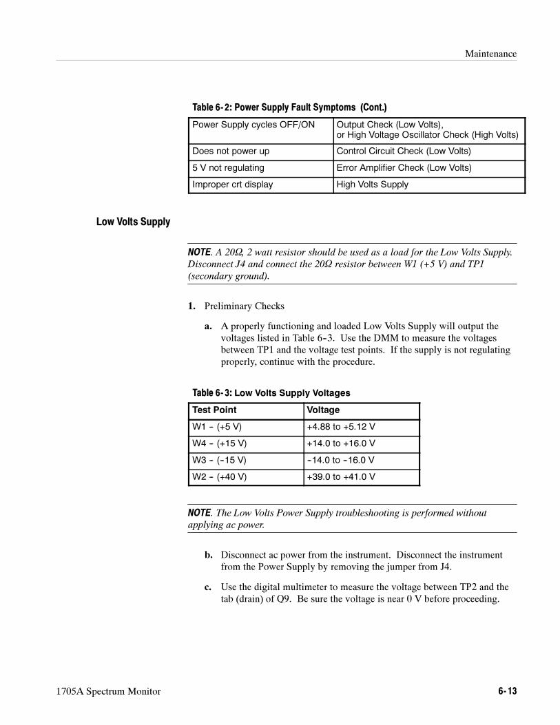
Maintenance
1705A Spectrum Monitor 6- 13
Table 6- 2: Power Supply Fault Symptoms (Cont.)
Power Supply cycles OFF/ON Output Check (Low Volts),or High Voltage Oscillator Check (High Volts)
Does not power up Control Circuit Check (Low Volts)
5 V not regulating Error Amplifier Check (Low Volts)
Improper crt display High Volts Supply
NOTE. A 20Ω, 2 watt resistor should be used as a load for the Low Volts Supply.
Disconnect J4 and connect the 20Ω resistor between W1 (+5 V) and TP1
(secondary ground).
1. Preliminary Checks
a. A properly functioning and loaded Low Volts Supply will output thevoltages listed in Table 6--3. Use the DMM to measure the voltagesbetween TP1 and the voltage test points. If the supply is not regulatingproperly, continue with the procedure.
Table 6- 3: Low Volts Supply Voltages
Test Point Voltage
W1 -- (+5 V) +4.88 to +5.12 V
W4 -- (+15 V) +14.0 to +16.0 V
W3 -- (--15 V) --14.0 to --16.0 V
W2 -- (+40 V) +39.0 to +41.0 V
NOTE. The Low Volts Power Supply troubleshooting is performed without
applying ac power.
b. Disconnect ac power from the instrument. Disconnect the instrumentfrom the Power Supply by removing the jumper from J4.
c. Use the digital multimeter to measure the voltage between TP2 and thetab (drain) of Q9. Be sure the voltage is near 0 V before proceeding.
Low Volts Supply
Maintenance
6- 14 1705A Spectrum Monitor
CAUTION. Do not proceed until the drain of Q9 is near 0 V. Dangerous voltage
potentials are present in the circuit until the capacitors discharge.
2. Rectifier/Switcher Check
a. Use the digital multimeter to measure the voltage between TP2 and thetab (drain) of Q9. Be sure the voltage is near 0 V before proceeding.
b. Unsolder and lift one end of R102.
c. With the negative lead of the digital multimeter connected to TP2 andthe positive lead connected to the tab of Q9, measure the circuitresistance. A resistance of less than 20 kΩ indicates a shorted mosfet(Q9). If the mosfet is shorted, replace it and perform the Control CircuitCheck.
d. Using the digital multimeter diode test function, test CR21, CR22,CR23, and CR24 for shorts. Diode replacements must be fast reverserecovery (300 ns) types to reduce conducted noise.
e. Reconnect the lifted end of R102.
3. Output Check
a. Connect the negative output from the 20 Vdc Power Supply to TP1.Connect the positive output to W4 (+15 V). The circuit should draw lessthan 20 mA. Excessive current draw can be caused by CR11 or U2(High Volts Power Supply).
b. Connect the negative output from the 20 Vdc Power Supply to TP1.Connect the positive output to W2 (+40 V). The circuit should draw lessthan 20 mA. Excessive current draw can be caused by CR14 or Q6(High Volts Power Supply).
c. Connect the positive output from the 20 Vdc Power Supply to TP1.Connect the negative output to W3 (--15 V). The circuit should drawless than 20 mA. Excessive current draw can be caused by CR12.
d. Connect the negative output from the 5 Vdc Power Supply to TP1.Connect the positive output to W1 (+5 V). The circuit should draw lessthan 20 mA. Excessive current draw can be caused by CR13 or Q1 andQ2 (High Volts Power Supply).
4. Control Circuit Check
a. Connect the negative output from the 20 Vdc Power Supply to TP2.Connect the positive output to the cathode of CR17. Short C47 with aclip lead. Connect the oscilloscope probe ground to TP2.
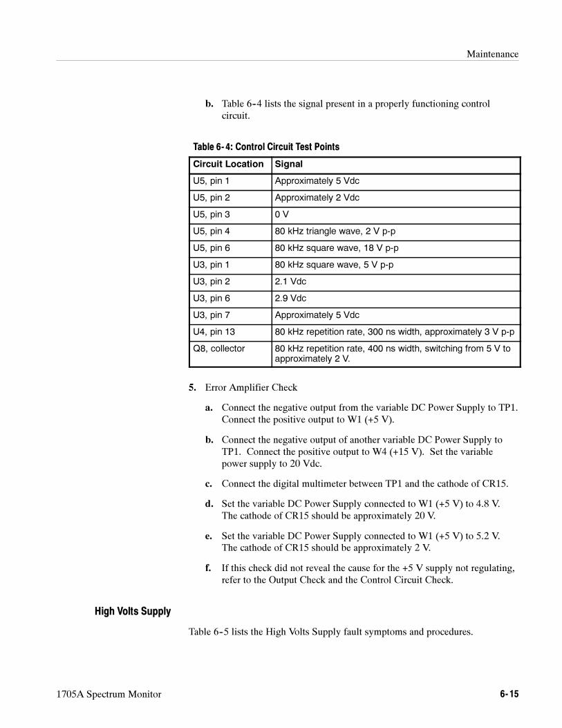
Maintenance
1705A Spectrum Monitor 6- 15
b. Table 6--4 lists the signal present in a properly functioning controlcircuit.
Table 6- 4: Control Circuit Test Points
Circuit Location Signal
U5, pin 1 Approximately 5 Vdc
U5, pin 2 Approximately 2 Vdc
U5, pin 3 0 V
U5, pin 4 80 kHz triangle wave, 2 V p-p
U5, pin 6 80 kHz square wave, 18 V p-p
U3, pin 1 80 kHz square wave, 5 V p-p
U3, pin 2 2.1 Vdc
U3, pin 6 2.9 Vdc
U3, pin 7 Approximately 5 Vdc
U4, pin 13 80 kHz repetition rate, 300 ns width, approximately 3 V p-p
Q8, collector 80 kHz repetition rate, 400 ns width, switching from 5 V toapproximately 2 V.
5. Error Amplifier Check
a. Connect the negative output from the variable DC Power Supply to TP1.Connect the positive output to W1 (+5 V).
b. Connect the negative output of another variable DC Power Supply toTP1. Connect the positive output to W4 (+15 V). Set the variablepower supply to 20 Vdc.
c. Connect the digital multimeter between TP1 and the cathode of CR15.
d. Set the variable DC Power Supply connected to W1 (+5 V) to 4.8 V.The cathode of CR15 should be approximately 20 V.
e. Set the variable DC Power Supply connected to W1 (+5 V) to 5.2 V.The cathode of CR15 should be approximately 2 V.
f. If this check did not reveal the cause for the +5 V supply not regulating,refer to the Output Check and the Control Circuit Check.
Table 6--5 lists the High Volts Supply fault symptoms and procedures.
High Volts Supply
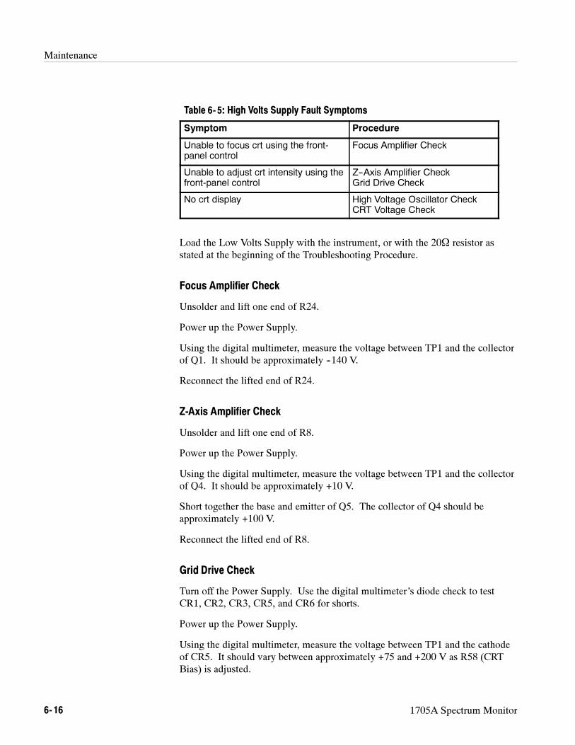
Maintenance
6- 16 1705A Spectrum Monitor
Table 6- 5: High Volts Supply Fault Symptoms
Symptom Procedure
Unable to focus crt using the front-panel control
Focus Amplifier Check
Unable to adjust crt intensity using thefront-panel control
Z--Axis Amplifier CheckGrid Drive Check
No crt display High Voltage Oscillator CheckCRT Voltage Check
Load the Low Volts Supply with the instrument, or with the 20Ω resistor asstated at the beginning of the Troubleshooting Procedure.
Focus Amplifier Check
Unsolder and lift one end of R24.
Power up the Power Supply.
Using the digital multimeter, measure the voltage between TP1 and the collectorof Q1. It should be approximately --140 V.
Reconnect the lifted end of R24.
Z-Axis Amplifier Check
Unsolder and lift one end of R8.
Power up the Power Supply.
Using the digital multimeter, measure the voltage between TP1 and the collectorof Q4. It should be approximately +10 V.
Short together the base and emitter of Q5. The collector of Q4 should beapproximately +100 V.
Reconnect the lifted end of R8.
Grid Drive Check
Turn off the Power Supply. Use the digital multimeter’s diode check to testCR1, CR2, CR3, CR5, and CR6 for shorts.
Power up the Power Supply.
Using the digital multimeter, measure the voltage between TP1 and the cathodeof CR5. It should vary between approximately +75 and +200 V as R58 (CRTBias) is adjusted.
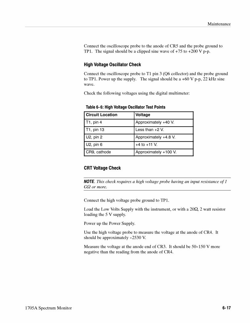
Maintenance
1705A Spectrum Monitor 6- 17
Connect the oscilloscope probe to the anode of CR5 and the probe ground toTP1. The signal should be a clipped sine wave of +75 to +200 V p-p.
High Voltage Oscillator Check
Connect the oscilloscope probe to T1 pin 3 (Q6 collector) and the probe groundto TP1. Power up the supply. The signal should be a +60 V p-p, 22 kHz sinewave.
Check the following voltages using the digital multimeter:
Table 6- 6: High Voltage Oscillator Test Points
Circuit Location Voltage
T1, pin 4 Approximately +40 V.
T1, pin 13 Less than +2 V.
U2, pin 2 Approximately +4.8 V.
U2, pin 6 +4 to +11 V.
CR9, cathode Approximately +100 V.
CRT Voltage Check
NOTE. This check requires a high voltage probe having an input resistance of 1
GΩ or more.
Connect the high voltage probe ground to TP1.
Load the Low Volts Supply with the instrument, or with a 20Ω, 2 watt resistorloading the 5 V supply.
Power up the Power Supply.
Use the high voltage probe to measure the voltage at the anode of CR4. Itshould be approximately --2530 V.
Measure the voltage at the anode end of CR3. It should be 50--150 V morenegative than the reading from the anode of CR4.
Maintenance
6- 18 1705A Spectrum Monitor
CORRECTIVE MAINTENANCE
CAUTION. A 2% RMA flux content solder is recommended for making repairs in
this instrument. Cleaning of rosin residue is not recommended. Most cleaning
solvents tend to reactivate the rosin and spread it under components where it
may cause corrosion under humid conditions. The rosin residue, if left alone,
does not exhibit these corrosive properties.
NOTE. No repair should be attempted during the warranty period.
Obtaining Replacement Parts
Replacement parts are available through the local Tektronix, Inc., field office orrepresentative. However, many common electronic parts are available throughlocal sources. Using a local source, where possible, will eliminate shippingdelays.
Changes to Tektronix instruments are sometimes made to accommodateimproved components, as they become available, and to improve circuitperformance. Therefore, it is important to include the following informationwhen ordering parts:
1. Part Number
2. Instrument Type or Number
3. Serial Number
4. Modification or Option Number (if applicable)
If an ordered part has been replaced with a new or improved part that is a directreplacement, the new part will be shipped. If the part does not directly replacethe old one, the local Tektronix field office or representative will contact thecustomer. After any repair or modification of the instrument, circuit readjust-ment may be required.
Test selectable components and their values are shown in Table 6---7.Test SelectedComponents
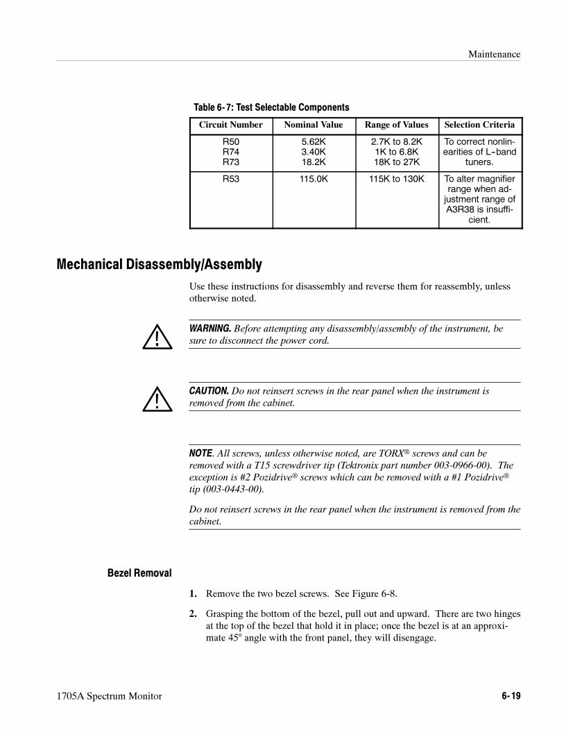
Maintenance
1705A Spectrum Monitor 6- 19
Table 6- 7: Test Selectable Components
Circuit Number Nominal Value Range of Values Selection Criteria
R50R74R73
5.62K3.40K18.2K
2.7K to 8.2K1K to 6.8K18K to 27K
To correct nonlin-earities of L--band
tuners.
R53 115.0K 115K to 130K To alter magnifierrange when ad-justment range ofA3R38 is insuffi-
cient.
Mechanical Disassembly/Assembly
Use these instructions for disassembly and reverse them for reassembly, unlessotherwise noted.
WARNING. Before attempting any disassembly/assembly of the instrument, be
sure to disconnect the power cord.
CAUTION. Do not reinsert screws in the rear panel when the instrument is
removed from the cabinet.
NOTE. All screws, unless otherwise noted, are TORX screws and can be
removed with a T15 screwdriver tip (Tektronix part number 003-0966-00). The
exception is #2 Pozidrive screws which can be removed with a #1 Pozidrive
tip (003-0443-00).
Do not reinsert screws in the rear panel when the instrument is removed from the
cabinet.
1. Remove the two bezel screws. See Figure 6-8.
2. Grasping the bottom of the bezel, pull out and upward. There are two hingesat the top of the bezel that hold it in place; once the bezel is at an approxi-mate 45° angle with the front panel, they will disengage.
Bezel Removal
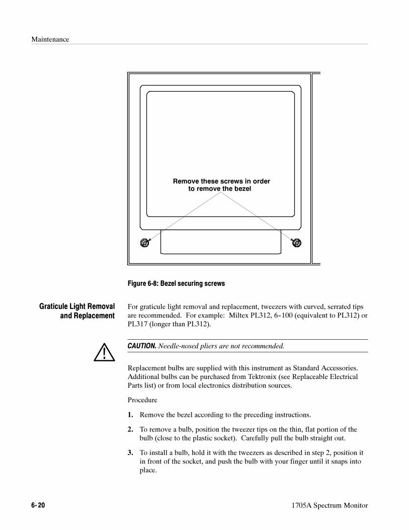
Maintenance
6- 20 1705A Spectrum Monitor
Remove these screws in orderto remove the bezel
Figure 6-8: Bezel securing screws
For graticule light removal and replacement, tweezers with curved, serrated tipsare recommended. For example: Miltex PL312, 6--100 (equivalent to PL312) orPL317 (longer than PL312).
CAUTION. Needle-nosed pliers are not recommended.
Replacement bulbs are supplied with this instrument as Standard Accessories.Additional bulbs can be purchased from Tektronix (see Replaceable ElectricalParts list) or from local electronics distribution sources.
Procedure
1. Remove the bezel according to the preceding instructions.
2. To remove a bulb, position the tweezer tips on the thin, flat portion of thebulb (close to the plastic socket). Carefully pull the bulb straight out.
3. To install a bulb, hold it with the tweezers as described in step 2, position itin front of the socket, and push the bulb with your finger until it snaps intoplace.
Graticule Light Removaland Replacement
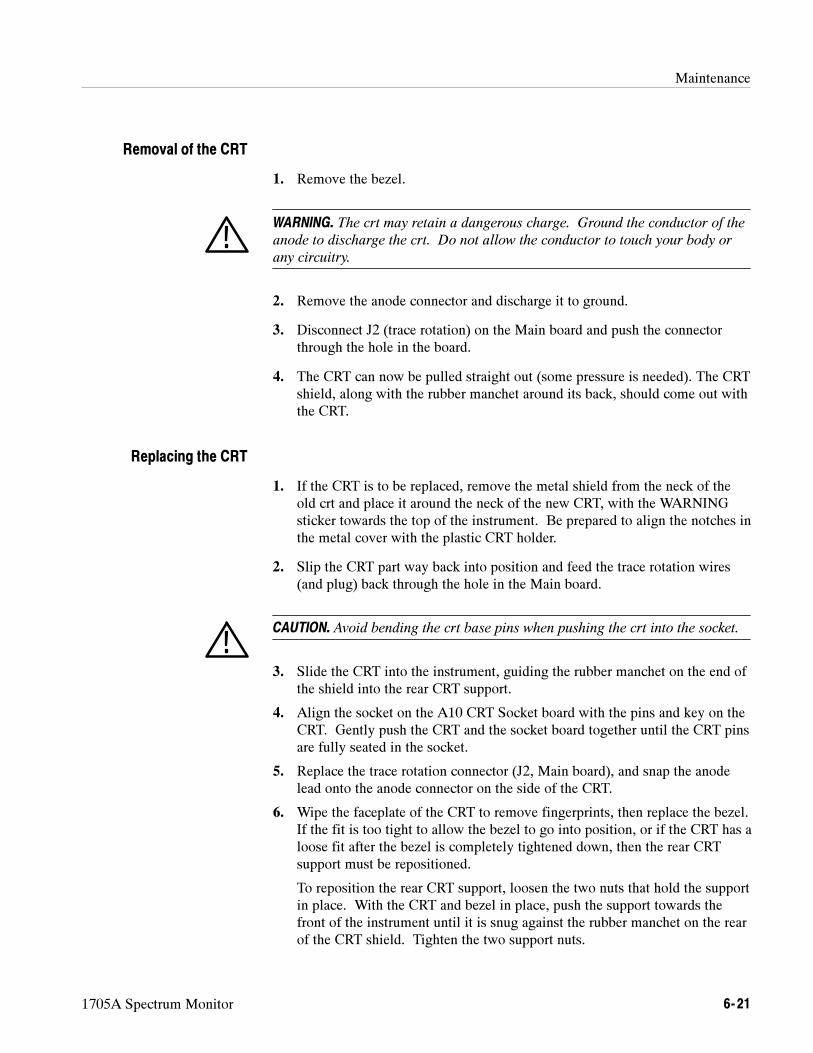
Maintenance
1705A Spectrum Monitor 6- 21
1. Remove the bezel.
WARNING. The crt may retain a dangerous charge. Ground the conductor of the
anode to discharge the crt. Do not allow the conductor to touch your body or
any circuitry.
2. Remove the anode connector and discharge it to ground.
3. Disconnect J2 (trace rotation) on the Main board and push the connectorthrough the hole in the board.
4. The CRT can now be pulled straight out (some pressure is needed). The CRTshield, along with the rubber manchet around its back, should come out withthe CRT.
1. If the CRT is to be replaced, remove the metal shield from the neck of theold crt and place it around the neck of the new CRT, with the WARNINGsticker towards the top of the instrument. Be prepared to align the notches inthe metal cover with the plastic CRT holder.
2. Slip the CRT part way back into position and feed the trace rotation wires(and plug) back through the hole in the Main board.
CAUTION. Avoid bending the crt base pins when pushing the crt into the socket.
3. Slide the CRT into the instrument, guiding the rubber manchet on the end ofthe shield into the rear CRT support.
4. Align the socket on the A10 CRT Socket board with the pins and key on theCRT. Gently push the CRT and the socket board together until the CRT pinsare fully seated in the socket.
5. Replace the trace rotation connector (J2, Main board), and snap the anodelead onto the anode connector on the side of the CRT.
6. Wipe the faceplate of the CRT to remove fingerprints, then replace the bezel.If the fit is too tight to allow the bezel to go into position, or if the CRT has aloose fit after the bezel is completely tightened down, then the rear CRTsupport must be repositioned.
To reposition the rear CRT support, loosen the two nuts that hold the supportin place. With the CRT and bezel in place, push the support towards thefront of the instrument until it is snug against the rubber manchet on the rearof the CRT shield. Tighten the two support nuts.
Removal of the CRT
Replacing the CRT
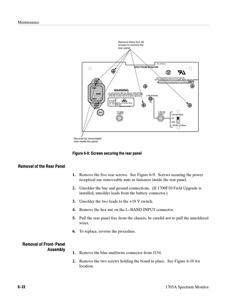
Maintenance
6- 22 1705A Spectrum Monitor
BESCHLEUNIGUNGSSPANNUNG KLEINERALS20kV
DIE IN DIESEM GERATENTSTEHENDE
RONTGENSTRAHLUNG IST AUSREICHENDABGESCHIRMT
TO AVOID ELECTRICAL SHOCK, THE POWERCORD PROTECTIVEGROUNDING CONDUCTORMUST BECONNECTEDTO EARTH GROUND.
SPECTRUM MONITOR
70 MHzINPUT
L-BANDINPUT
LNB POWER
LNB POWER
ON
OFF
+18VDC@250mA
Remove these five (5)screws to remove therear panel.
Secured by removeablenuts inside the panel.
ON
WARNING
0.70 MAX50/60Hz
90 - 250VREPLACE FUSEONLYWITH
250V 2A F TYPE
333--3990--01
Figure 6-9: Screws securing the rear panel
1. Remove the five rear screws. See Figure 6-9. Screws securing the powerreceptical use removeable nuts as fasteners inside the rear panel.
2. Unsolder the bnc and ground connections. (If 1700F10 Field Upgrade isinstalled, unsolder leads from the battery connector.)
3. Unsolder the two leads to the +18 V switch.
4. Remove the hex nut on the L--BAND INPUT connector.
5. Pull the rear panel free from the chassis, be careful not to pull the unsolderedwires.
6. To replace, reverse the procedure.
1. Remove the blue multiwire connector from J154.
2. Remove the two screws holding the board in place. See Figure 6-10 forlocation.
Removal of the Rear Panel
Removal of Front- PanelAssembly
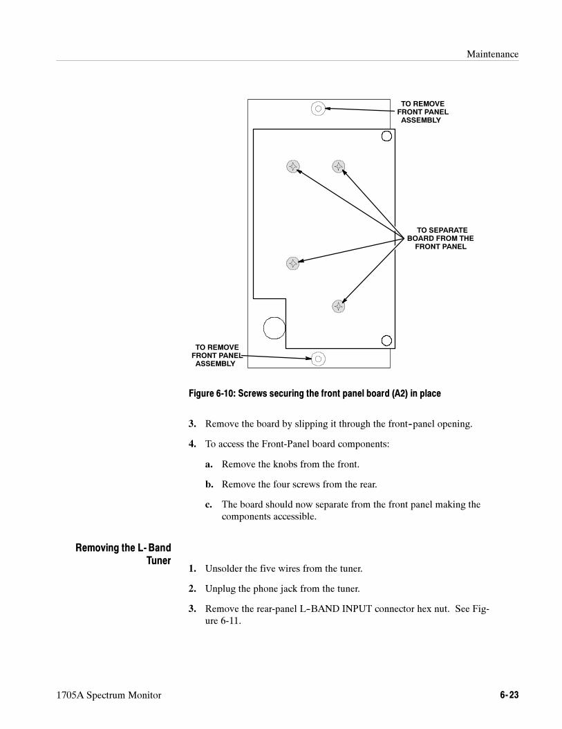
Maintenance
1705A Spectrum Monitor 6- 23
TO REMOVEFRONT PANELASSEMBLY
TO REMOVEFRONT PANELASSEMBLY
TO SEPARATEBOARD FROM THE
FRONT PANEL
Figure 6-10: Screws securing the front panel board (A2) in place
3. Remove the board by slipping it through the front--panel opening.
4. To access the Front-Panel board components:
a. Remove the knobs from the front.
b. Remove the four screws from the rear.
c. The board should now separate from the front panel making thecomponents accessible.
1. Unsolder the five wires from the tuner.
2. Unplug the phone jack from the tuner.
3. Remove the rear-panel L--BAND INPUT connector hex nut. See Fig-ure 6-11.
Removing the L- BandTuner
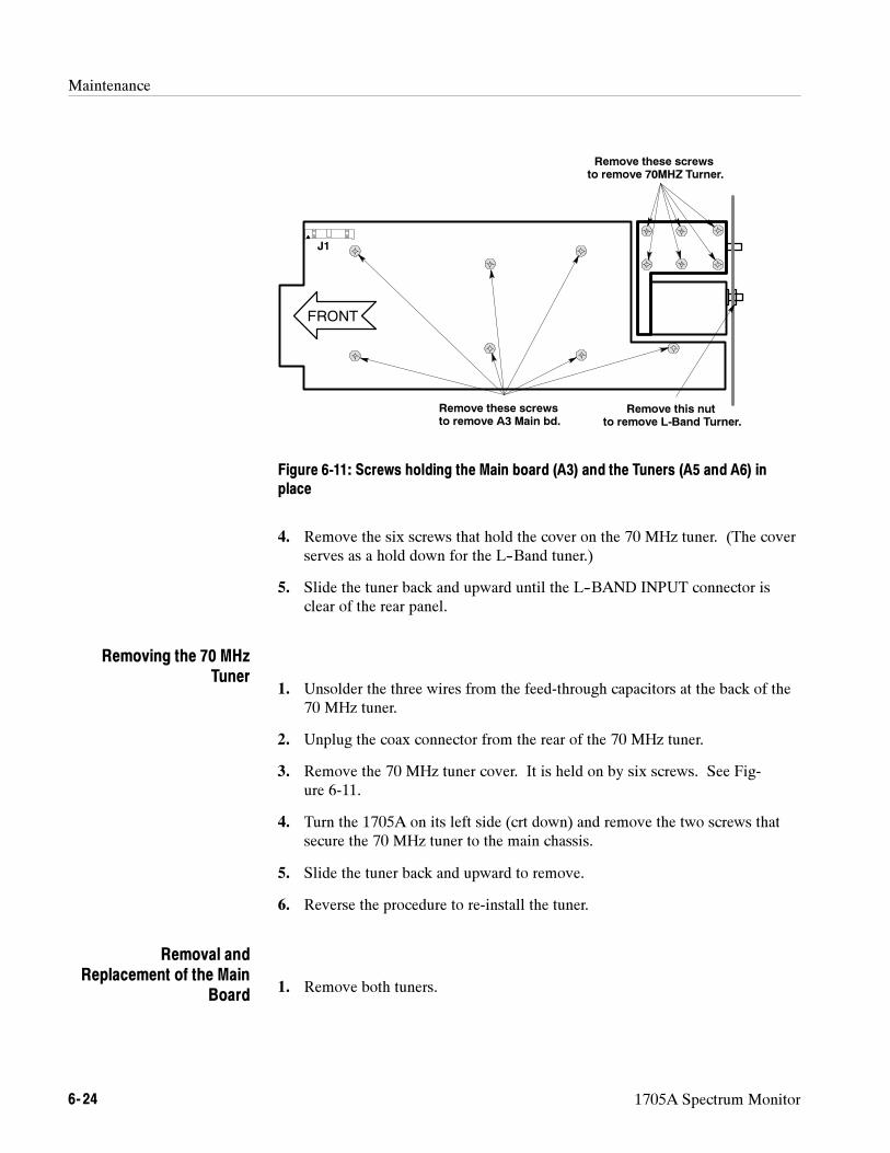
Maintenance
6- 24 1705A Spectrum Monitor
FRONT
J1
Remove these screwsto remove A3 Main bd.
Remove these screwsto remove 70MHZ Turner.
Remove this nutto remove L-Band Turner.
Figure 6-11: Screws holding the Main board (A3) and the Tuners (A5 and A6) inplace
4. Remove the six screws that hold the cover on the 70 MHz tuner. (The coverserves as a hold down for the L--Band tuner.)
5. Slide the tuner back and upward until the L--BAND INPUT connector isclear of the rear panel.
1. Unsolder the three wires from the feed-through capacitors at the back of the70 MHz tuner.
2. Unplug the coax connector from the rear of the 70 MHz tuner.
3. Remove the 70 MHz tuner cover. It is held on by six screws. See Fig-ure 6-11.
4. Turn the 1705A on its left side (crt down) and remove the two screws thatsecure the 70 MHz tuner to the main chassis.
5. Slide the tuner back and upward to remove.
6. Reverse the procedure to re-install the tuner.
1. Remove both tuners.
Removing the 70 MHzTuner
Removal andReplacement of the Main
Board
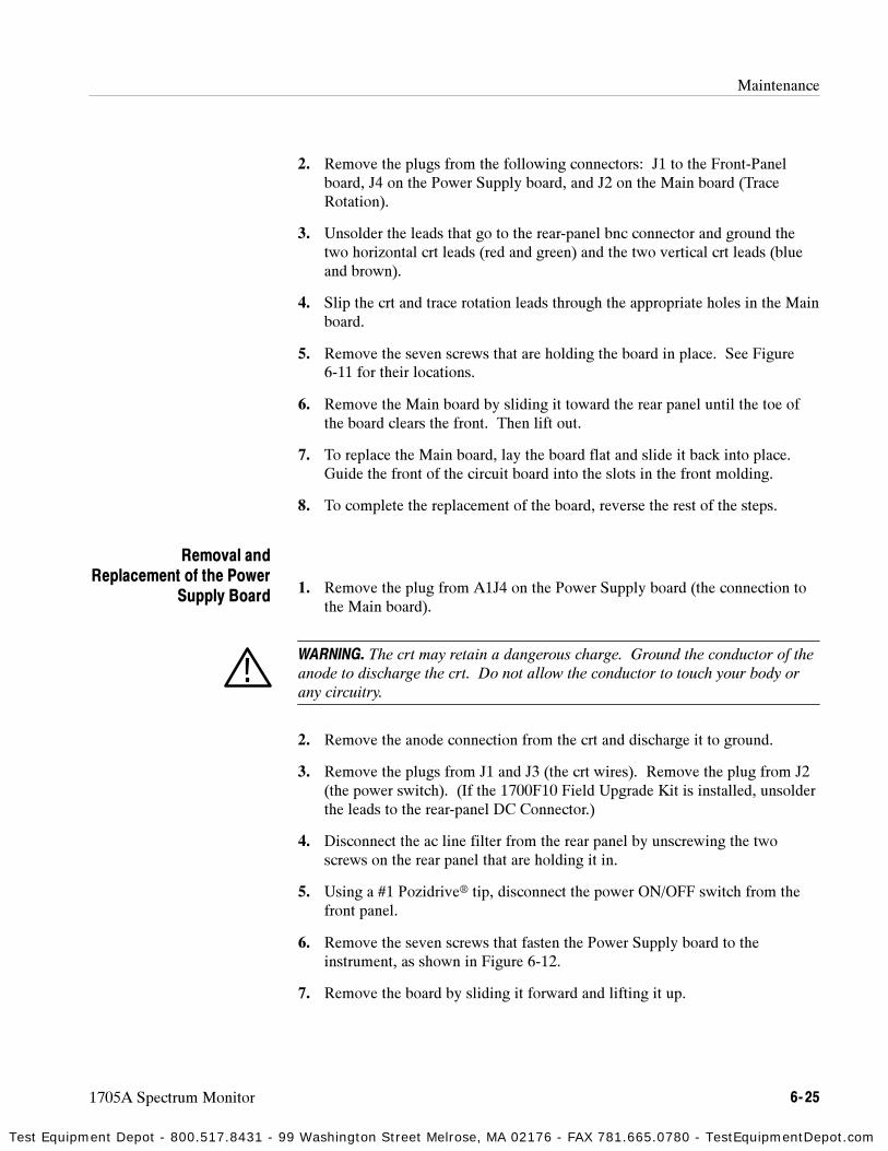
Maintenance
1705A Spectrum Monitor 6- 25
2. Remove the plugs from the following connectors: J1 to the Front-Panelboard, J4 on the Power Supply board, and J2 on the Main board (TraceRotation).
3. Unsolder the leads that go to the rear-panel bnc connector and ground thetwo horizontal crt leads (red and green) and the two vertical crt leads (blueand brown).
4. Slip the crt and trace rotation leads through the appropriate holes in the Mainboard.
5. Remove the seven screws that are holding the board in place. See Figure6-11 for their locations.
6. Remove the Main board by sliding it toward the rear panel until the toe ofthe board clears the front. Then lift out.
7. To replace the Main board, lay the board flat and slide it back into place.Guide the front of the circuit board into the slots in the front molding.
8. To complete the replacement of the board, reverse the rest of the steps.
1. Remove the plug from A1J4 on the Power Supply board (the connection tothe Main board).
WARNING. The crt may retain a dangerous charge. Ground the conductor of the
anode to discharge the crt. Do not allow the conductor to touch your body or
any circuitry.
2. Remove the anode connection from the crt and discharge it to ground.
3. Remove the plugs from J1 and J3 (the crt wires). Remove the plug from J2(the power switch). (If the 1700F10 Field Upgrade Kit is installed, unsolderthe leads to the rear-panel DC Connector.)
4. Disconnect the ac line filter from the rear panel by unscrewing the twoscrews on the rear panel that are holding it in.
5. Using a #1 Pozidrive tip, disconnect the power ON/OFF switch from thefront panel.
6. Remove the seven screws that fasten the Power Supply board to theinstrument, as shown in Figure 6-12.
7. Remove the board by sliding it forward and lifting it up.
Removal andReplacement of the Power
Supply Board
Test Equipment Depot - 800.517.8431 - 99 Washington Street Melrose, MA 02176 - FAX 781.665.0780 - TestEquipmentDepot.com
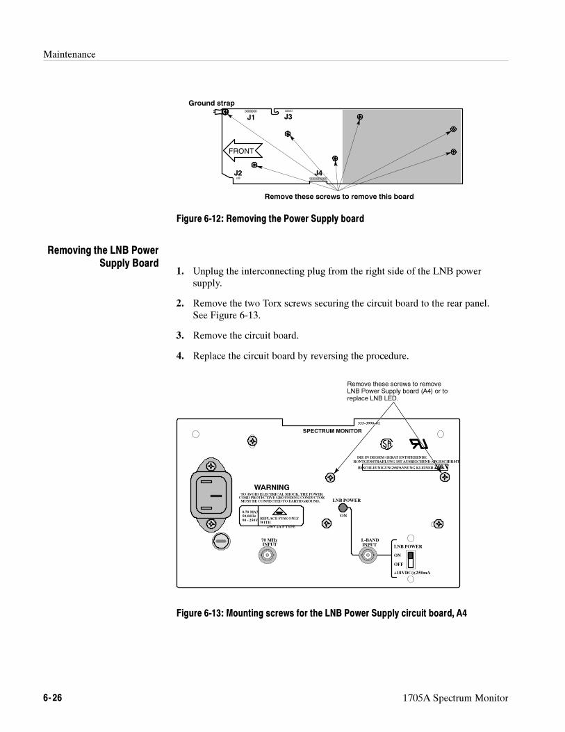
Maintenance
6- 26 1705A Spectrum Monitor
FRONT
J1 J3
J2 J4
Ground strap
Remove these screws to remove this board
Figure 6-12: Removing the Power Supply board
1. Unplug the interconnecting plug from the right side of the LNB powersupply.
2. Remove the two Torx screws securing the circuit board to the rear panel.See Figure 6-13.
3. Remove the circuit board.
4. Replace the circuit board by reversing the procedure.
BESCHLEUNIGUNGSSPANNUNG KLEINERALS20kV
DIE IN DIESEM GERATENTSTEHENDE
RONTGENSTRAHLUNG IST AUSREICHENDABGESCHIRMT
TO AVOID ELECTRICAL SHOCK, THE POWERCORD PROTECTIVEGROUNDING CONDUCTORMUST BECONNECTEDTO EARTH GROUND.
SPECTRUM MONITOR
70 MHzINPUT
L-BANDINPUT
LNB POWER
LNB POWER
ON
OFF
+18VDC@250mA
ON
WARNING
0.70 MAX50/60Hz
90 - 250VREPLACE FUSEONLYWITH
250V 2A F TYPE
333--3990--01
Remove these screws to removeLNB Power Supply board (A4) or toreplace LNB LED.
Figure 6-13: Mounting screws for the LNB Power Supply circuit board, A4
Removing the LNB PowerSupply Board
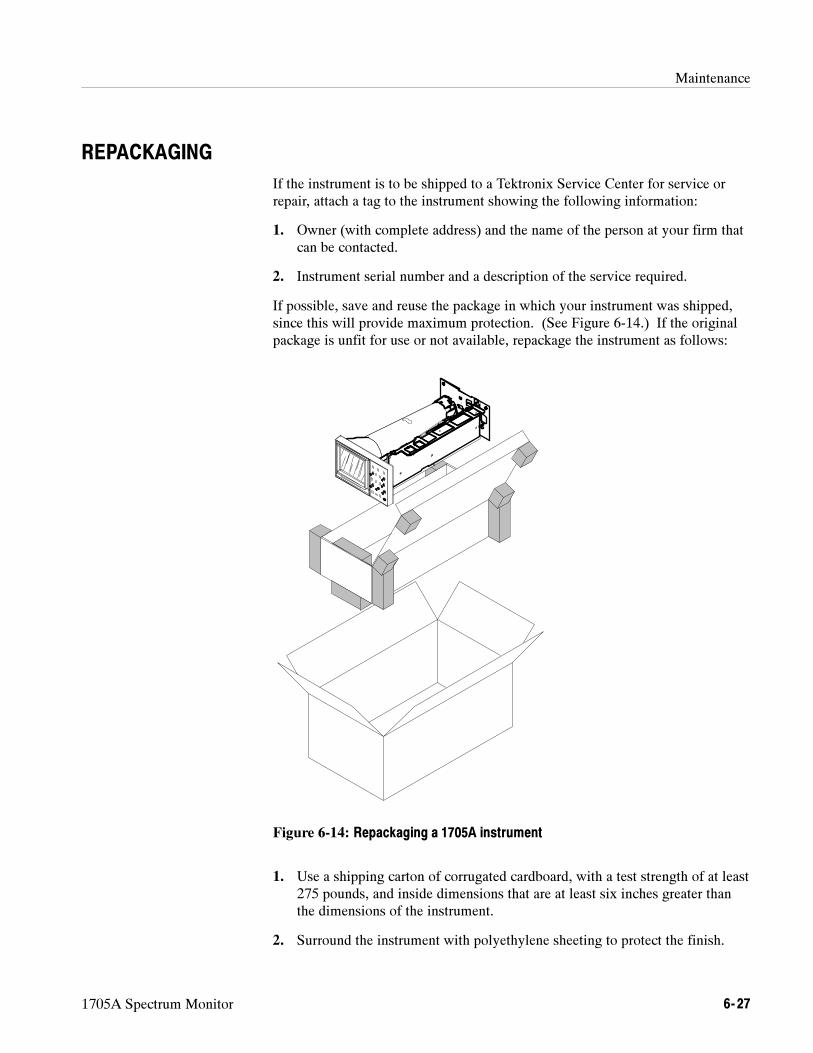
Maintenance
1705A Spectrum Monitor 6- 27
REPACKAGING
If the instrument is to be shipped to a Tektronix Service Center for service orrepair, attach a tag to the instrument showing the following information:
1. Owner (with complete address) and the name of the person at your firm thatcan be contacted.
2. Instrument serial number and a description of the service required.
If possible, save and reuse the package in which your instrument was shipped,since this will provide maximum protection. (See Figure 6-14.) If the originalpackage is unfit for use or not available, repackage the instrument as follows:
Figure 6-14: Repackaging a 1705A instrument
1. Use a shipping carton of corrugated cardboard, with a test strength of at least275 pounds, and inside dimensions that are at least six inches greater thanthe dimensions of the instrument.
2. Surround the instrument with polyethylene sheeting to protect the finish.

Maintenance
6- 28 1705A Spectrum Monitor
3. Cushion the instrument on all sides by tightly packing dunnage or urethanefoam between the carton and the instrument. Allow 3 inches on all sides forcushioning.
4. Seal the carton with shipping tape or industrial stapler.

Options

1705A Spectrum Monitor 7- 1
Section 7Options
This section describes instrument options and customer-installable field upgradekits available for the 1705A Spectrum Monitor.
Options
The standard instrument is shipped with a P31 (green) phosphor crt installed. IfOption 74 is ordered, the instrument is shipped with a P4 (white) phosphor crtinstalled. The crt part numbers are given at the end of the Replaceable ElectricalParts list.
Table 7- 1: Power Cord Options
Option Description of power cord*
A1 Universal Europe 220V/16A Locking
A2 United Kingdom 240V/15A
A3 Australian 240V/10A
A4 North American 250V/18A
A5 Swiss 240V/6A
*All power cords include captive power plug and one replacement fuse.
Unless otherwise specified, power cords for use in North America are UL listedand CSA certified. Option cords are approved by at least one test houseacceptable in the country to which the product is shipped. Power cord partnumbers are shown on the pull-out in Section 10.
Field Upgrade Kits
All of the Safety and EMI tests used to qualify the 1705A were performed in acabinet. There are two optional cabinets and a dual rack adapter available for theinstallation of these instruments.
For more information, refer to the cabinet installation drawings in Section 3, orcontact a Tektronix field office or distributor.
CRT Options
Power Cord Options
Cabinets
Options
7- 2 1705A Spectrum Monitor
Plain Cabinet (1700F00) This plain, silver-grey cabinet is designed for permanentmounting. The ventilating holes in the top, bottom, and sides of the cabinetallow heat generated within the instrument to dissipate. When mounting, allowair to circulate freely through these holes.
Carrying Case (1700F02) This silver-grey metal cabinet, designed for portableapplications, is equipped with feet, flipstand, and carrying handle. TheTEKTRONIX BP1 Battery Pack can easily be mounted to this cabinet to providea 12 Vdc power source for portable operation.
Side- by- Side Rack Adapter (WFM7F05) This side-by-side rack adapter consistsof two attached cabinets. It can be used to mount the 1705A and anotherhalf-rack width instrument in a standard 19-inch rack.
Blank Panel (1700F06) When only one side of a 1700F05 dual rack adapter isused, this blank panel can be installed in the other half to improve appearanceand protect air flow.
Utility Drawer (1700F07)When only one side of a 1700F05 dual rack adapter isused, an alternate to the 1700F06 blank panel is the 1700F07 utility drawer. Thisdrawer provides over 1/3 cubic foot of storage space for accessories. The drawerkit includes a tray, which is permanently mounted to the 1700F05. The draweropens and closes readily, unless latched for transport. The drawer can also beremoved from the drawer tray by lifting up and out.
ORDERING
These items can be ordered with the 1705A, or purchased through a Tektronixfield office or distributor. When ordering, include both the name and number ofthe field upgrade kits.

Replaceable Electrical Parts

1705A Spectrum Monitor 8- 1
Section 8Replaceable Electrical Parts
This section contains a list of the components that are replaceable for the 1705A.Use this list to identify and order replacement parts. There is a separateReplaceable Electrical Parts list for each instrument.
Parts Ordering InformationReplacement parts are available from or through your local Tektronix, Inc., FieldOffice or representative.
Changes to Tektronix instruments are sometimes made to accommodateimproved components as they become available and to give you the benefit ofthe latest circuit improvements. Therefore, when ordering parts, it is important toinclude the following information in your order.
Part number Instrument type or model number Instrument serial number Instrument modification number, if applicable
If a part you have ordered has been replaced with a new or improved part, yourlocal Tektronix, Inc., Field Office or representative will contact you concerningany change in part number.
Change information, if any, is located at the rear of this manual.
Using the Replaceable Electrical Parts ListThe tabular information in the Replaceable Electrical Parts list is arranged forquick retrieval. Understanding the structure and features of the list will help youfind all of the information you need for ordering replaceable parts.
The Mfg. Code Number to Manufacturer Cross Index for the electrical parts listis located immediately after this page. The cross index provides codes, names,and addresses of manufacturers of components listed in the electrical parts list.
Abbreviations conform to American National Standards Institute (ANSI)standard Y1.1.
A list of assemblies can be found at the beginning of the electrical parts list. Theassemblies are listed in numerical order. When the complete component numberof a part is known, this list will identify the assembly in which the part islocated.
Cross Index-Mfr. CodeNumber to Manufacturer
Abbreviations
List of Assemblies
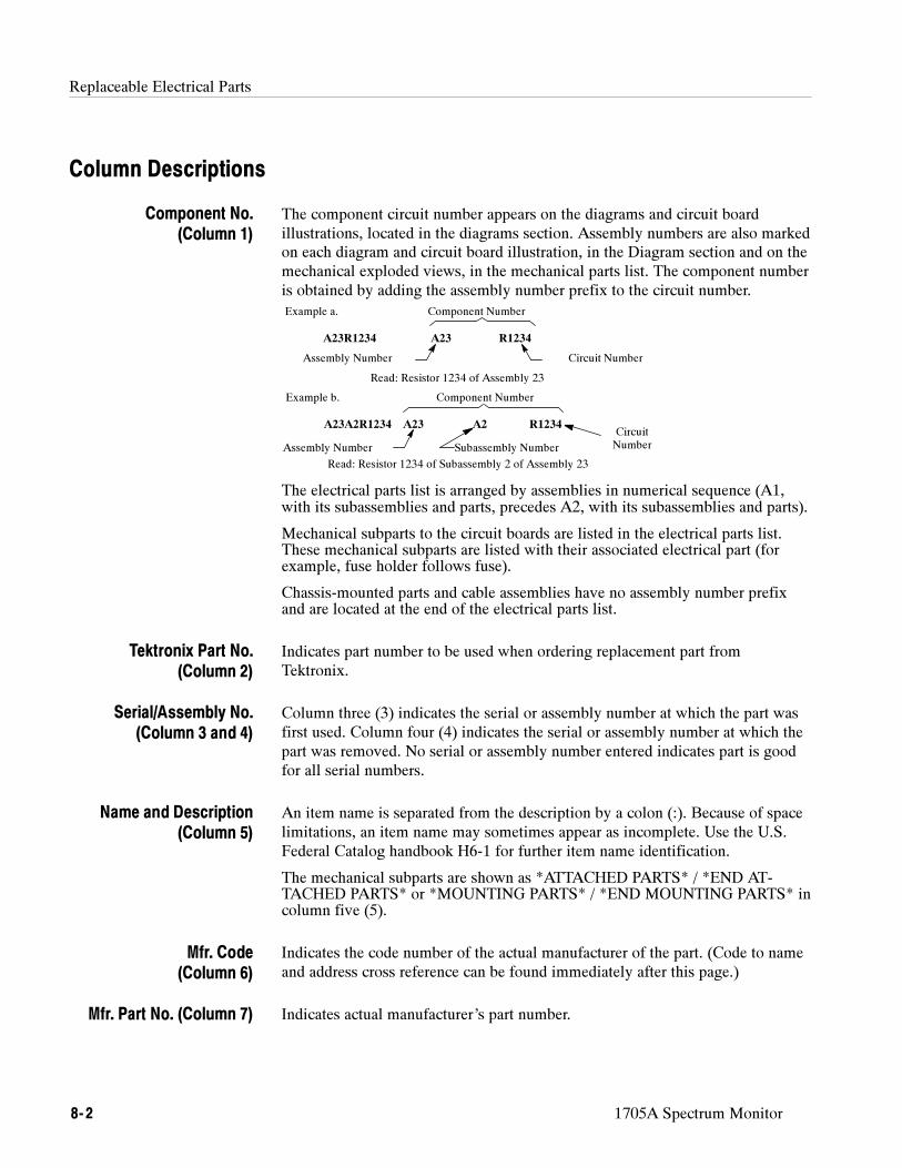
Replaceable Electrical Parts
8- 2 1705A Spectrum Monitor
Column Descriptions
The component circuit number appears on the diagrams and circuit boardillustrations, located in the diagrams section. Assembly numbers are also markedon each diagram and circuit board illustration, in the Diagram section and on themechanical exploded views, in the mechanical parts list. The component numberis obtained by adding the assembly number prefix to the circuit number.
Example a. Component Number
A23R1234 A23 R1234
Assembly Number Circuit Number
Read: Resistor 1234 of Assembly 23
Example b. Component Number
A23A2R1234 A23 R1234
Assembly Number
CircuitNumber
Read: Resistor 1234 of Subassembly 2 of Assembly 23
A2
Subassembly Number
The electrical parts list is arranged by assemblies in numerical sequence (A1,with its subassemblies and parts, precedes A2, with its subassemblies and parts).
Mechanical subparts to the circuit boards are listed in the electrical parts list.These mechanical subparts are listed with their associated electrical part (forexample, fuse holder follows fuse).
Chassis-mounted parts and cable assemblies have no assembly number prefixand are located at the end of the electrical parts list.
Indicates part number to be used when ordering replacement part fromTektronix.
Column three (3) indicates the serial or assembly number at which the part wasfirst used. Column four (4) indicates the serial or assembly number at which thepart was removed. No serial or assembly number entered indicates part is goodfor all serial numbers.
An item name is separated from the description by a colon (:). Because of spacelimitations, an item name may sometimes appear as incomplete. Use the U.S.Federal Catalog handbook H6-1 for further item name identification.
The mechanical subparts are shown as *ATTACHED PARTS* / *END AT-TACHED PARTS* or *MOUNTING PARTS* / *END MOUNTING PARTS* incolumn five (5).
Indicates the code number of the actual manufacturer of the part. (Code to nameand address cross reference can be found immediately after this page.)
Indicates actual manufacturer’s part number.
Component No.(Column 1)
Tektronix Part No.(Column 2)
Serial/Assembly No.(Column 3 and 4)
Name and Description(Column 5)
Mfr. Code(Column 6)
Mfr. Part No. (Column 7)
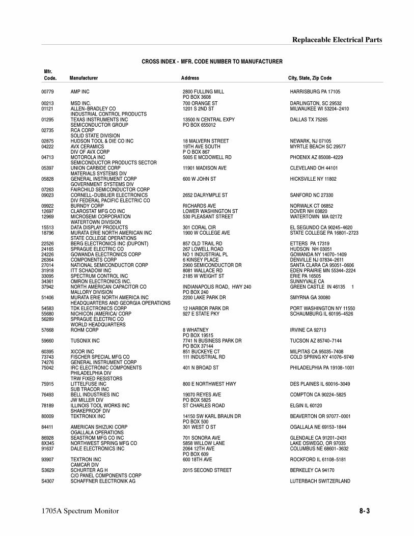
Replaceable Electrical Parts
1705A Spectrum Monitor 8- 3
CROSS INDEX - MFR. CODE NUMBER TO MANUFACTURER
Mfr.
Code. Manufacturer Address City, State, Zip Code
00779 AMP INC 2800 FULLING MILL HARRISBURG PA 17105PO BOX 3608
00213 MSD INC. 700 ORANGE ST DARLINGTON, SC 2953201121 ALLEN--BRADLEY CO 1201 S 2ND ST MILWAUKEE WI 53204--2410
INDUSTRIAL CONTROL PRODUCTS01295 TEXAS INSTRUMENTS INC 13500 N CENTRAL EXPY DALLAS TX 75265
SEMICONDUCTOR GROUP PO BOX 65501202735 RCA CORP
SOLID STATE DIVISION02875 HUDSON TOOL & DIE CO INC 18 MALVERN STREET NEWARK, NJ 0710504222 AVX CERAMICS 19TH AVE SOUTH MYRTLE BEACH SC 29577
DIV OF AVX CORP P O BOX 86704713 MOTOROLA INC 5005 E MCDOWELL RD PHOENIX AZ 85008--4229
SEMICONDUCTOR PRODUCTS SECTOR05397 UNION CARBIDE CORP 11901 MADISON AVE CLEVELAND OH 44101
MATERIALS SYSTEMS DIV05828 GENERAL INSTRUMENT CORP 600 W JOHN ST HICKSVILLE NY 11802
GOVERNMENT SYSTEMS DIV07263 FAIRCHILD SEMICONDUCTOR CORP09023 CORNELL--DUBILIER ELECTRONICS 2652 DALRYMPLE ST SANFORD NC 27330
DIV FEDERAL PACIFIC ELECTRIC CO09922 BURNDY CORP RICHARDS AVE NORWALK CT 0685212697 CLAROSTAT MFG CO INC LOWER WASHINGTON ST DOVER NH 0382012969 MICROSEMI CORPORATION 530 PLEASANT STREET WATERTOWN MA 02172
WATERTOWN DIVISION15513 DATA DISPLAY PRODUCTS 301 CORAL CIR EL SEGUNDO CA 90245--462018796 MURATA ERIE NORTH AMERICAN INC 1900 W COLLEGE AVE STATE COLLEGE PA 16801--2723
STATE COLLEGE OPERATIONS22526 BERG ELECTRONICS INC (DUPONT) 857 OLD TRAIL RD ETTERS PA 1731924165 SPRAGUE ELECTRIC CO 267 LOWELL ROAD HUDSON NH 0305124226 GOWANDA ELECTRONICS CORP NO 1 INDUSTRIAL PL GOWANDA NY 14070--140926364 COMPONENTS CORP 6 KINSEY PLACE DENVILLE NJ 07834--261127014 NATIONAL SEMICONDUCTOR CORP 2900 SEMICONDUCTOR DR SANTA CLARA CA 95051--060631918 ITT SCHADOW INC 8081 WALLACE RD EDEN PRAIRIE MN 55344--222433095 SPECTRUM CONTROL INC 2185 W WEIGHT ST ERIE PA 1650534361 OMRON ELECTRONICS INC. SUNNYVALE CA37942 NORTH AMERICAN CAPACITOR CO INDIANAPOLIS ROAD, HWY 240 GREEN CASTLE IN 46135 1
MALLORY DIVISION PO BOX 24051406 MURATA ERIE NORTH AMERICA INC 2200 LAKE PARK DR SMYRNA GA 30080
HEADQUARTERS AND GEORGIA OPERATIONS54583 TDK ELECTRONICS CORP 12 HARBOR PARK DR PORT WASHINGTON NY 1155055680 NICHICON /AMERICA/ CORP 927 E STATE PKY SCHAUMBURG IL 60195--452656289 SPRAGUE ELECTRIC CO
WORLD HEADQUARTERS57668 ROHM CORP 8 WHATNEY IRVINE CA 92713
PO BOX 1951559660 TUSONIX INC 7741 N BUSINESS PARK DR TUCSON AZ 85740--7144
PO BOX 3714460395 XICOR INC 851 BUCKEYE CT MILPITAS CA 95035--740873743 FISCHER SPECIAL MFG CO 111 INDUSTRIAL RD COLD SPRING KY 41076--974974276 GENERAL INSTRUMENT CORP75042 IRC ELECTRONIC COMPONENTS 401 N BROAD ST PHILADELPHIA PA 19108--1001
PHILADELPHIA DIVTRW FIXED RESISTORS
75915 LITTELFUSE INC 800 E NORTHWEST HWY DES PLAINES IL 60016--3049SUB TRACOR INC
76493 BELL INDUSTRIES INC 19070 REYES AVE COMPTON CA 90224--5825JW MILLER DIV PO BOX 5825
78189 ILLINOIS TOOL WORKS INC ST CHARLES ROAD ELGIN IL 60120SHAKEPROOF DIV
80009 TEKTRONIX INC 14150 SW KARL BRAUN DR BEAVERTON OR 97077--0001PO BOX 500
84411 AMERICAN SHIZUKI CORP 301 WEST O ST OGALLALA NE 69153--1844OGALLALA OPERATIONS
86928 SEASTROM MFG CO INC 701 SONORA AVE GLENDALE CA 91201--24318X345 NORTHWEST SPRING MFG CO 5858 WILLOW LANE LAKE OSWEGO, OR 9703591637 DALE ELECTRONICS INC 2064 12TH AVE COLUMBUS NE 68601--3632
PO BOX 60993907 TEXTRON INC 600 18TH AVE ROCKFORD IL 61108--5181
CAMCAR DIVS3629 SCHURTER AG H 2015 SECOND STREET BERKELEY CA 94170
C/O PANEL COMPONENTS CORPS4307 SCHAFFNER ELECTRONIK AG LUTERBACH SWITZERLAND
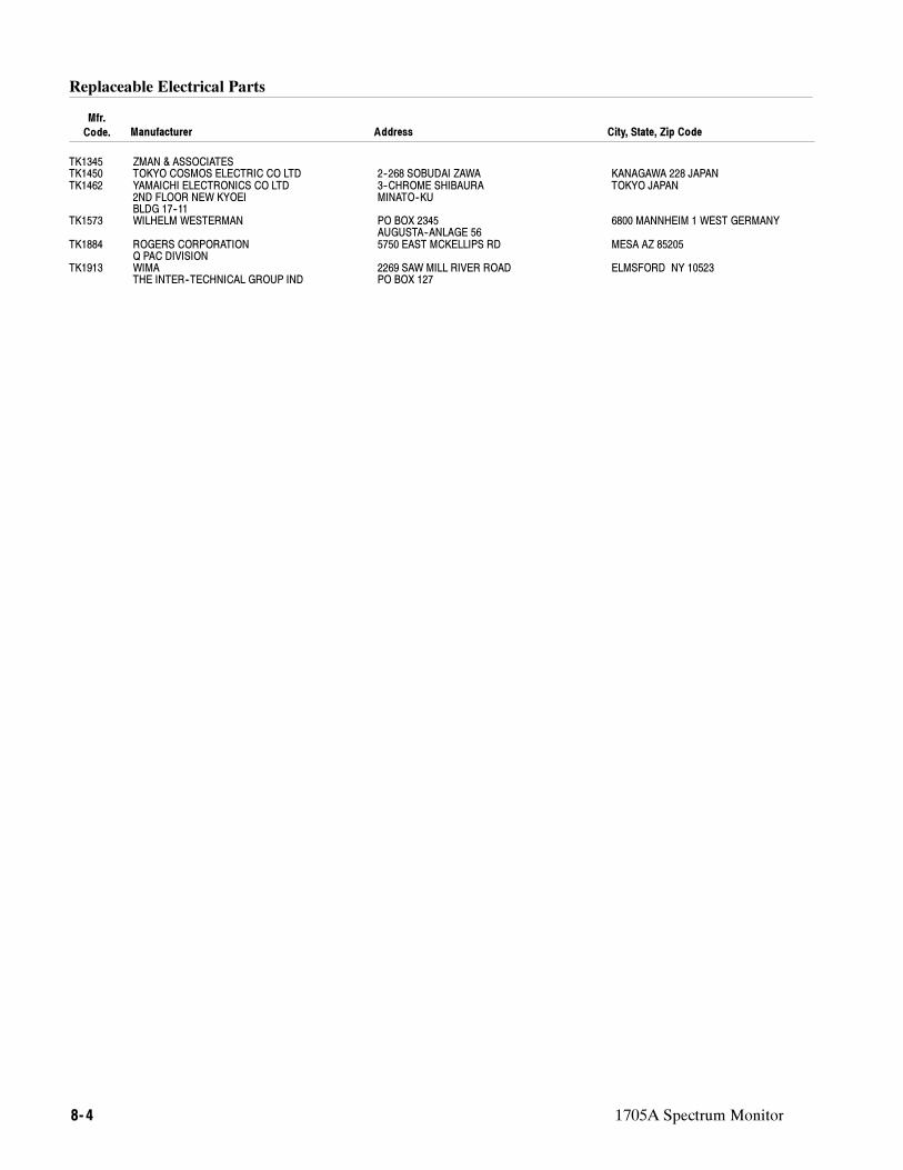
Replaceable Electrical Parts
8- 4 1705A Spectrum Monitor
Mfr.
Code. Manufacturer Address City, State, Zip Code
TK1345 ZMAN & ASSOCIATESTK1450 TOKYO COSMOS ELECTRIC CO LTD 2--268 SOBUDAI ZAWA KANAGAWA 228 JAPANTK1462 YAMAICHI ELECTRONICS CO LTD 3--CHROME SHIBAURA TOKYO JAPAN
2ND FLOOR NEW KYOEI MINATO--KUBLDG 17--11
TK1573 WILHELM WESTERMAN PO BOX 2345 6800 MANNHEIM 1 WEST GERMANYAUGUSTA--ANLAGE 56
TK1884 ROGERS CORPORATION 5750 EAST MCKELLIPS RD MESA AZ 85205Q PAC DIVISION
TK1913 WIMA 2269 SAW MILL RIVER ROAD ELMSFORD NY 10523THE INTER--TECHNICAL GROUP IND PO BOX 127
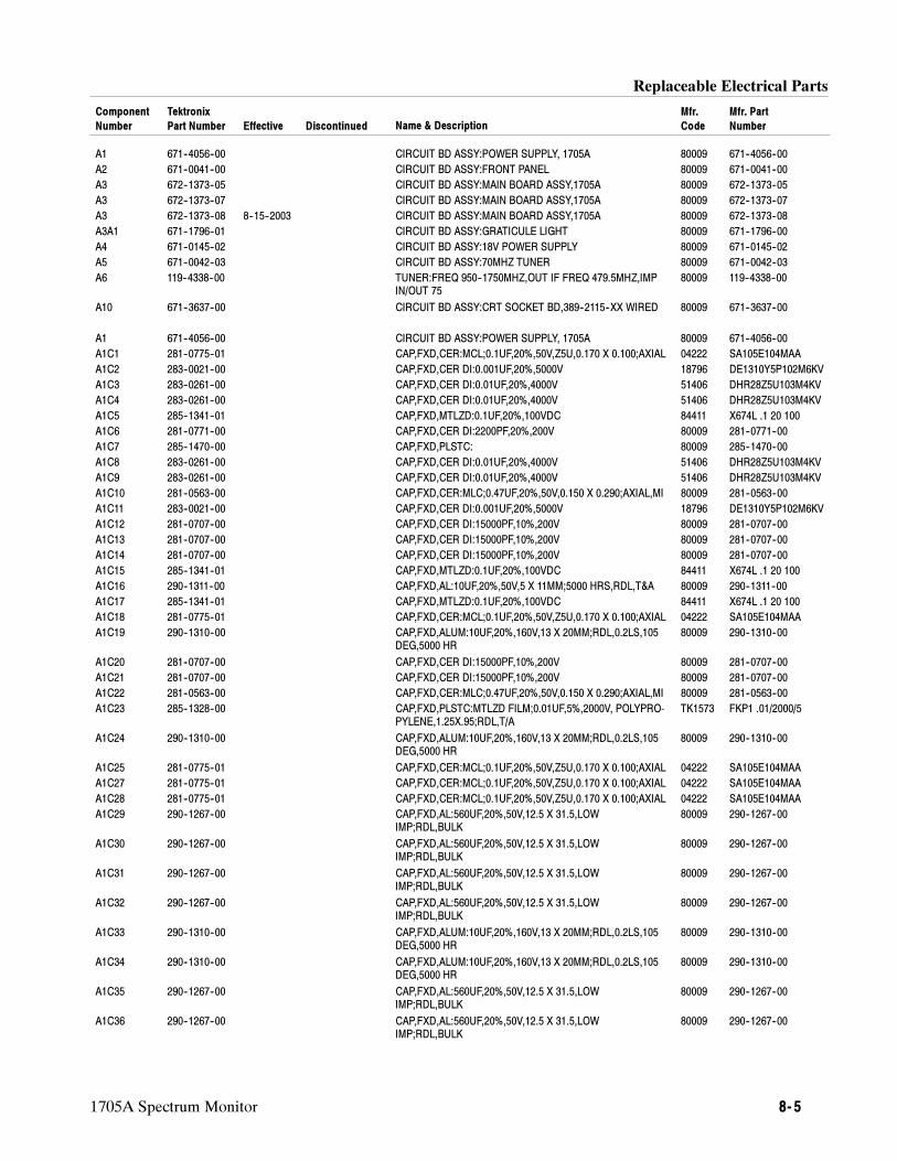
Replaceable Electrical Parts
1705A Spectrum Monitor 8- 5
Component
Number
Tektronix
Part Number Effective Discontinued Name & Description
Mfr.
Code
Mfr. Part
Number
A1 671--4056--00 CIRCUIT BD ASSY:POWER SUPPLY, 1705A 80009 671--4056--00
A2 671--0041--00 CIRCUIT BD ASSY:FRONT PANEL 80009 671--0041--00
A3 672--1373--05 CIRCUIT BD ASSY:MAIN BOARD ASSY,1705A 80009 672--1373--05
A3 672--1373--07 CIRCUIT BD ASSY:MAIN BOARD ASSY,1705A 80009 672--1373--07
A3 672--1373--08 8--15--2003 CIRCUIT BD ASSY:MAIN BOARD ASSY,1705A 80009 672--1373--08
A3A1 671--1796--01 CIRCUIT BD ASSY:GRATICULE LIGHT 80009 671--1796--00
A4 671--0145--02 CIRCUIT BD ASSY:18V POWER SUPPLY 80009 671--0145--02
A5 671--0042--03 CIRCUIT BD ASSY:70MHZ TUNER 80009 671--0042--03
A6 119--4338--00 TUNER:FREQ 950--1750MHZ,OUT IF FREQ 479.5MHZ,IMPIN/OUT 75
80009 119--4338--00
A10 671--3637--00 CIRCUIT BD ASSY:CRT SOCKET BD,389--2115--XX WIRED 80009 671--3637--00
A1 671--4056--00 CIRCUIT BD ASSY:POWER SUPPLY, 1705A 80009 671--4056--00
A1C1 281--0775--01 CAP,FXD,CER:MCL;0.1UF,20%,50V,Z5U,0.170 X 0.100;AXIAL 04222 SA105E104MAA
A1C2 283--0021--00 CAP,FXD,CER DI:0.001UF,20%,5000V 18796 DE1310Y5P102M6KV
A1C3 283--0261--00 CAP,FXD,CER DI:0.01UF,20%,4000V 51406 DHR28Z5U103M4KV
A1C4 283--0261--00 CAP,FXD,CER DI:0.01UF,20%,4000V 51406 DHR28Z5U103M4KV
A1C5 285--1341--01 CAP,FXD,MTLZD:0.1UF,20%,100VDC 84411 X674L .1 20 100
A1C6 281--0771--00 CAP,FXD,CER DI:2200PF,20%,200V 80009 281--0771--00
A1C7 285--1470--00 CAP,FXD,PLSTC: 80009 285--1470--00
A1C8 283--0261--00 CAP,FXD,CER DI:0.01UF,20%,4000V 51406 DHR28Z5U103M4KV
A1C9 283--0261--00 CAP,FXD,CER DI:0.01UF,20%,4000V 51406 DHR28Z5U103M4KV
A1C10 281--0563--00 CAP,FXD,CER:MLC;0.47UF,20%,50V,0.150 X 0.290;AXIAL,MI 80009 281--0563--00
A1C11 283--0021--00 CAP,FXD,CER DI:0.001UF,20%,5000V 18796 DE1310Y5P102M6KV
A1C12 281--0707--00 CAP,FXD,CER DI:15000PF,10%,200V 80009 281--0707--00
A1C13 281--0707--00 CAP,FXD,CER DI:15000PF,10%,200V 80009 281--0707--00
A1C14 281--0707--00 CAP,FXD,CER DI:15000PF,10%,200V 80009 281--0707--00
A1C15 285--1341--01 CAP,FXD,MTLZD:0.1UF,20%,100VDC 84411 X674L .1 20 100
A1C16 290--1311--00 CAP,FXD,AL:10UF,20%,50V,5 X 11MM;5000 HRS,RDL,T&A 80009 290--1311--00
A1C17 285--1341--01 CAP,FXD,MTLZD:0.1UF,20%,100VDC 84411 X674L .1 20 100
A1C18 281--0775--01 CAP,FXD,CER:MCL;0.1UF,20%,50V,Z5U,0.170 X 0.100;AXIAL 04222 SA105E104MAA
A1C19 290--1310--00 CAP,FXD,ALUM:10UF,20%,160V,13 X 20MM;RDL,0.2LS,105DEG,5000 HR
80009 290--1310--00
A1C20 281--0707--00 CAP,FXD,CER DI:15000PF,10%,200V 80009 281--0707--00
A1C21 281--0707--00 CAP,FXD,CER DI:15000PF,10%,200V 80009 281--0707--00
A1C22 281--0563--00 CAP,FXD,CER:MLC;0.47UF,20%,50V,0.150 X 0.290;AXIAL,MI 80009 281--0563--00
A1C23 285--1328--00 CAP,FXD,PLSTC:MTLZD FILM;0.01UF,5%,2000V, POLYPRO-PYLENE,1.25X.95;RDL,T/A
TK1573 FKP1 .01/2000/5
A1C24 290--1310--00 CAP,FXD,ALUM:10UF,20%,160V,13 X 20MM;RDL,0.2LS,105DEG,5000 HR
80009 290--1310--00
A1C25 281--0775--01 CAP,FXD,CER:MCL;0.1UF,20%,50V,Z5U,0.170 X 0.100;AXIAL 04222 SA105E104MAA
A1C27 281--0775--01 CAP,FXD,CER:MCL;0.1UF,20%,50V,Z5U,0.170 X 0.100;AXIAL 04222 SA105E104MAA
A1C28 281--0775--01 CAP,FXD,CER:MCL;0.1UF,20%,50V,Z5U,0.170 X 0.100;AXIAL 04222 SA105E104MAA
A1C29 290--1267--00 CAP,FXD,AL:560UF,20%,50V,12.5 X 31.5,LOWIMP;RDL,BULK
80009 290--1267--00
A1C30 290--1267--00 CAP,FXD,AL:560UF,20%,50V,12.5 X 31.5,LOWIMP;RDL,BULK
80009 290--1267--00
A1C31 290--1267--00 CAP,FXD,AL:560UF,20%,50V,12.5 X 31.5,LOWIMP;RDL,BULK
80009 290--1267--00
A1C32 290--1267--00 CAP,FXD,AL:560UF,20%,50V,12.5 X 31.5,LOWIMP;RDL,BULK
80009 290--1267--00
A1C33 290--1310--00 CAP,FXD,ALUM:10UF,20%,160V,13 X 20MM;RDL,0.2LS,105DEG,5000 HR
80009 290--1310--00
A1C34 290--1310--00 CAP,FXD,ALUM:10UF,20%,160V,13 X 20MM;RDL,0.2LS,105DEG,5000 HR
80009 290--1310--00
A1C35 290--1267--00 CAP,FXD,AL:560UF,20%,50V,12.5 X 31.5,LOWIMP;RDL,BULK
80009 290--1267--00
A1C36 290--1267--00 CAP,FXD,AL:560UF,20%,50V,12.5 X 31.5,LOWIMP;RDL,BULK
80009 290--1267--00
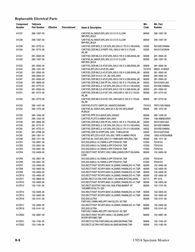
Replaceable Electrical Parts
8- 6 1705A Spectrum Monitor
Component
Number
Mfr. Part
Number
Mfr.
CodeName & DescriptionEffective Discontinued
Tektronix
Part Number
A1C37 290--1267--00 CAP,FXD,AL:560UF,20%,50V,12.5 X 31.5,LOWIMP;RDL,BULK
80009 290--1267--00
A1C38 290--1267--00 CAP,FXD,AL:560UF,20%,50V,12.5 X 31.5,LOWIMP;RDL,BULK
80009 290--1267--00
A1C39 281--0775--01 CAP,FXD,CER:MCL;0.1UF,20%,50V,Z5U,0.170 X 0.100;AXIAL 04222 SA105E104MAA
A1C40 281--0772--00 CAP,FXD,CER:MLC;4700PF,10%,100V,0.100 X 0.170;AX-IAL,MI
04222 SA101C472KAA
A1C41 281--0563--00 CAP,FXD,CER:MLC;0.47UF,20%,50V,0.150 X 0.290;AXIAL,MI 80009 281--0563--00
A1C42 290--1267--00 CAP,FXD,AL:560UF,20%,50V,12.5 X 31.5,LOWIMP;RDL,BULK
80009 290--1267--00
A1C43 281--0563--00 CAP,FXD,CER:MLC;0.47UF,20%,50V,0.150 X 0.290;AXIAL,MI 80009 281--0563--00
A1C44 285--1331--00 CAP,FXD,MTLZD:0.47UF,5%,400V TK1573 MKS4 .47/400/5
A1C45 281--0563--00 CAP,FXD,CER:MLC;0.47UF,20%,50V,0.150 X 0.290;AXIAL,MI 80009 281--0563--00
A1C46 283--0005--03 CAP,FXD,CER DI:0.01 UF,+80--20%,250V 80009 283--0005--03
A1C47 281--0563--00 CAP,FXD,CER:MLC;0.47UF,20%,50V,0.150 X 0.290;AXIAL,MI 80009 281--0563--00
A1C48 281--0809--00 CAP,FXD,CER:MLC;200 PF,5%,100V,0.100 X 0.170;AXIAL,MI 04222 SA101A201JAA
A1C49 281--0775--01 CAP,FXD,CER:MCL;0.1UF,20%,50V,Z5U,0.170 X 0.100;AXIAL 04222 SA105E104MAA
A1C50 281--0563--00 CAP,FXD,CER:MLC;0.47UF,20%,50V,0.150 X 0.290;AXIAL,MI 80009 281--0563--00
A1C51 281--0773--00 CAP,FXD,CER:MLC;0.01UF,10%,100V,SAF,0.100 X 0.170;AX-IAL,MI
80009 281--0773--00
A1C52 281--0773--00 CAP,FXD,CER:MLC;0.01UF,10%,100V,SAF,0.100 X 0.170;AX-IAL,MI
80009 281--0773--00
A1C53 285--1437--00 CAP,FXD,PLSTC:100PF,5%,1600VDC/500VAC TK1913 FKP1/100/1600/5
A1C54 290--1275--00 CAP,FXD,AL:330UF,20%,400V,35 X 35;105 DEG,SNAPIN,BULK
80009 290--1275--00
A1C56 285--1246--00 CAP,FXD,PPR DI:0.022UF,20%,250VAC 80009 285--1246--00
A1C57 285--1222--00 CAP,FXD,PLSTC:0.068UF,20%,250V 37942 158/.068/M/250/H
A1C58 281--0809--00 CAP,FXD,CER:MLC;200 PF,5%,100V,0.100 X 0.170;AXIAL,MI 04222 SA101A201JAA
A1C59 281--0775--01 CAP,FXD,CER:MCL;0.1UF,20%,50V,Z5U,0.170 X 0.100;AXIAL 04222 SA105E104MAA
A1C60 281--0775--01 CAP,FXD,CER:MCL;0.1UF,20%,50V,Z5U,0.170 X 0.100;AXIAL 04222 SA105E104MAA
A1C61 281--0768--00 CAP,FXD,CER DI:470PF,20%,100V TUBULAR,MI 04222 SA101A471KAA
A1C65 285--1301--01 CAP,FXD,MTLZD:0.47UF,10%,50V; TAPE & AMMO PACK 37942 185/0.47/K/50/AB/B
A1C66 290--1311--00 CAP,FXD,AL:10UF,20%,50V,5 X 11MM;5000 HRS,RDL,T&A 80009 290--1311--00
A1CR1 152--0061--00 DIO,SIG:200V,0.1A,700NS,4.0PF;FDH2161,T&R 07263 FDH2161
A1CR2 152--0061--00 DIO,SIG:200V,0.1A,700NS,4.0PF;FDH2161,T&R 07263 FDH2161
A1CR3 152--0061--00 DIO,SIG:200V,0.1A,700NS,4.0PF;FDH2161,T&R 07263 FDH2161
A1CR4 152--0409--00 DIO,RECT:FAST RCVRY;12KV,10MA,250NS;CRVT150,AXIALLEAD
80009 152--0409--00
A1CR5 152--0061--00 DIO,SIG:200V,0.1A,700NS,4.0PF;FDH2161,T&R 07263 FDH2161
A1CR6 152--0061--00 DIO,SIG:200V,0.1A,700NS,4.0PF;FDH2161,T&R 07263 FDH2161
A1CR7 152--0400--00 DIO,RECT:FAST RCVRY;400V,1A,200NS;1N4936,DO--41,T&R 80009 152--0400--00
A1CR8 152--0400--00 DIO,RECT:FAST RCVRY;400V,1A,200NS;1N4936,DO--41,T&R 80009 152--0400--00
A1CR9 152--0400--00 DIO,RECT:FAST RCVRY;400V,1A,200NS;1N4936,DO--41,T&R 80009 152--0400--00
A1CR10 152--0400--00 DIO,RECT:FAST RCVRY;400V,1A,200NS;1N4936,DO--41,T&R 80009 152--0400--00
A1CR11 152--0808--00 DIODE,RECT:ULTRA FAST,400V,1.5A,50NS,BYD73G,AXIAL 04713 PR 1273
A1CR12 152--0400--00 DIO,RECT:FAST RCVRY;400V,1A,200NS;1N4936,DO--41,T&R 80009 152--0400--00
A1CR13 152--1191--00 DIO,RECT:SCHTKY;100V,10A,150A IFSM,800MVF AT10A;MBR10100,TO--220
80009 152--1191--00
A1CR14 152--0400--00 DIO,RECT:FAST RCVRY;400V,1A,200NS;1N4936,DO--41,T&R 80009 152--0400--00
A1CR15 152--0400--00 DIO,RECT:FAST RCVRY;400V,1A,200NS;1N4936,DO--41,T&R 80009 152--0400--00
A1CR16 152--0141--02 DIO,SIG:ULTRAFAST;40V,150MA,4NS,2PF;1N4152,DO--35,T&R
80009 152--0141--02
A1CR17 152--0400--00 DIO,RECT:FAST RCVRY;400V,1A,200NS;1N4936,DO--41,T&R 80009 152--0400--00
A1CR19 152--0141--02 DIO,SIG:ULTRAFAST;40V,150MA,4NS,2PF;1N4152,DO--35,T&R
80009 152--0141--02
A1CR20 152--0897--00 DIO,RECT:FAST RCVRY;1000V,1.5A,300NS,SOFTRCVRY;BYV96E,T&R
80009 152--0897--00
A1CR21 152--1165--00 DIO,RECT:ULTRA FAST;600V,4A,50NS;MUR460,T&R 80009 152--1165--00
A1CR22 152--1165--00 DIO,RECT:ULTRA FAST;600V,4A,50NS;MUR460,T&R 80009 152--1165--00
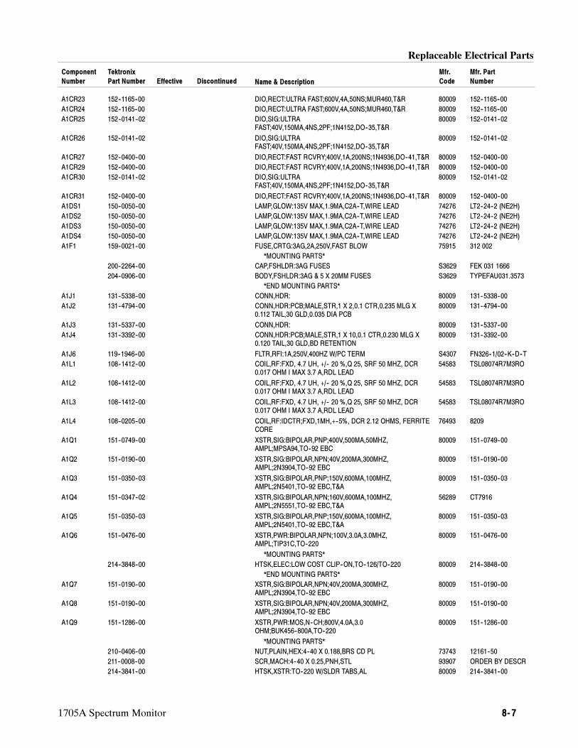
Replaceable Electrical Parts
1705A Spectrum Monitor 8- 7
Component
Number
Mfr. Part
Number
Mfr.
CodeName & DescriptionEffective Discontinued
Tektronix
Part Number
A1CR23 152--1165--00 DIO,RECT:ULTRA FAST;600V,4A,50NS;MUR460,T&R 80009 152--1165--00
A1CR24 152--1165--00 DIO,RECT:ULTRA FAST;600V,4A,50NS;MUR460,T&R 80009 152--1165--00
A1CR25 152--0141--02 DIO,SIG:ULTRAFAST;40V,150MA,4NS,2PF;1N4152,DO--35,T&R
80009 152--0141--02
A1CR26 152--0141--02 DIO,SIG:ULTRAFAST;40V,150MA,4NS,2PF;1N4152,DO--35,T&R
80009 152--0141--02
A1CR27 152--0400--00 DIO,RECT:FAST RCVRY;400V,1A,200NS;1N4936,DO--41,T&R 80009 152--0400--00
A1CR29 152--0400--00 DIO,RECT:FAST RCVRY;400V,1A,200NS;1N4936,DO--41,T&R 80009 152--0400--00
A1CR30 152--0141--02 DIO,SIG:ULTRAFAST;40V,150MA,4NS,2PF;1N4152,DO--35,T&R
80009 152--0141--02
A1CR31 152--0400--00 DIO,RECT:FAST RCVRY;400V,1A,200NS;1N4936,DO--41,T&R 80009 152--0400--00
A1DS1 150--0050--00 LAMP,GLOW:135V MAX,1.9MA,C2A--T,WIRE LEAD 74276 LT2--24--2 (NE2H)
A1DS2 150--0050--00 LAMP,GLOW:135V MAX,1.9MA,C2A--T,WIRE LEAD 74276 LT2--24--2 (NE2H)
A1DS3 150--0050--00 LAMP,GLOW:135V MAX,1.9MA,C2A--T,WIRE LEAD 74276 LT2--24--2 (NE2H)
A1DS4 150--0050--00 LAMP,GLOW:135V MAX,1.9MA,C2A--T,WIRE LEAD 74276 LT2--24--2 (NE2H)
A1F1 159--0021--00 FUSE,CRTG:3AG,2A,250V,FAST BLOW 75915 312 002
*MOUNTING PARTS*
200--2264--00 CAP,FSHLDR:3AG FUSES S3629 FEK 031 1666
204--0906--00 BODY,FSHLDR:3AG & 5 X 20MM FUSES S3629 TYPEFAU031.3573
*END MOUNTING PARTS*
A1J1 131--5338--00 CONN,HDR: 80009 131--5338--00
A1J2 131--4794--00 CONN,HDR:PCB;MALE,STR,1 X 2,0.1 CTR,0.235 MLG X0.112 TAIL,30 GLD,0.035 DIA PCB
80009 131--4794--00
A1J3 131--5337--00 CONN,HDR: 80009 131--5337--00
A1J4 131--3392--00 CONN,HDR:PCB;MALE,STR,1 X 10,0.1 CTR,0.230 MLG X0.120 TAIL,30 GLD,BD RETENTION
80009 131--3392--00
A1J6 119--1946--00 FLTR,RFI:1A,250V,400HZ W/PC TERM S4307 FN326--1/02--K--D--T
A1L1 108--1412--00 COIL,RF:FXD, 4.7 UH, +/-- 20 %,Q 25, SRF 50 MHZ, DCR0.017 OHM I MAX 3.7 A,RDL LEAD
54583 TSL08074R7M3RO
A1L2 108--1412--00 COIL,RF:FXD, 4.7 UH, +/-- 20 %,Q 25, SRF 50 MHZ, DCR0.017 OHM I MAX 3.7 A,RDL LEAD
54583 TSL08074R7M3RO
A1L3 108--1412--00 COIL,RF:FXD, 4.7 UH, +/-- 20 %,Q 25, SRF 50 MHZ, DCR0.017 OHM I MAX 3.7 A,RDL LEAD
54583 TSL08074R7M3RO
A1L4 108--0205--00 COIL,RF:IDCTR;FXD,1MH,+--5%, DCR 2.12 OHMS, FERRITECORE
76493 8209
A1Q1 151--0749--00 XSTR,SIG:BIPOLAR,PNP;400V,500MA,50MHZ,AMPL;MPSA94,TO--92 EBC
80009 151--0749--00
A1Q2 151--0190--00 XSTR,SIG:BIPOLAR,NPN;40V,200MA,300MHZ,AMPL;2N3904,TO--92 EBC
80009 151--0190--00
A1Q3 151--0350--03 XSTR,SIG:BIPOLAR,PNP;150V,600MA,100MHZ,AMPL;2N5401,TO--92 EBC,T&A
80009 151--0350--03
A1Q4 151--0347--02 XSTR,SIG:BIPOLAR,NPN;160V,600MA,100MHZ,AMPL;2N5551,TO--92 EBC,T&A
56289 CT7916
A1Q5 151--0350--03 XSTR,SIG:BIPOLAR,PNP;150V,600MA,100MHZ,AMPL;2N5401,TO--92 EBC,T&A
80009 151--0350--03
A1Q6 151--0476--00 XSTR,PWR:BIPOLAR,NPN;100V,3.0A,3.0MHZ,AMPL;TIP31C,TO--220
80009 151--0476--00
*MOUNTING PARTS*
214--3848--00 HTSK,ELEC:LOW COST CLIP--ON,TO--126/TO--220 80009 214--3848--00
*END MOUNTING PARTS*
A1Q7 151--0190--00 XSTR,SIG:BIPOLAR,NPN;40V,200MA,300MHZ,AMPL;2N3904,TO--92 EBC
80009 151--0190--00
A1Q8 151--0190--00 XSTR,SIG:BIPOLAR,NPN;40V,200MA,300MHZ,AMPL;2N3904,TO--92 EBC
80009 151--0190--00
A1Q9 151--1286--00 XSTR,PWR:MOS,N--CH;800V,4.0A,3.0OHM;BUK456--800A,TO--220
80009 151--1286--00
*MOUNTING PARTS*
210--0406--00 NUT,PLAIN,HEX:4--40 X 0.188,BRS CD PL 73743 12161--50
211--0008--00 SCR,MACH:4--40 X 0.25,PNH,STL 93907 ORDER BY DESCR
214--3841--00 HTSK,XSTR:TO--220 W/SLDR TABS,AL 80009 214--3841--00
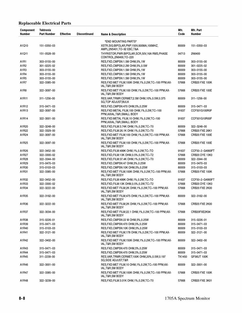
Replaceable Electrical Parts
8- 8 1705A Spectrum Monitor
Component
Number
Mfr. Part
Number
Mfr.
CodeName & DescriptionEffective Discontinued
Tektronix
Part Number
*END MOUNTING PARTS*
A1Q10 151--0350--03 XSTR,SIG:BIPOLAR,PNP;150V,600MA,100MHZ,AMPL;2N5401,TO--92 EBC,T&A
80009 151--0350--03
A1Q11 151--0528--00 THYRISTOR,PWR:BIPOLAR,SCR,50V,16A RMS,PHASECONTROL,2N6400,TO--220
04713 2N6400
A1R1 303--0155--00 RES,FXD,CMPSN:1.5M OHM,5%,1W 80009 303--0155--00
A1R2 301--0225--02 RES,FXD,CMPSN:2.2M OHM,5%,0.5W 80009 301--0225--02
A1R3 303--0155--00 RES,FXD,CMPSN:1.5M OHM,5%,1W 80009 303--0155--00
A1R4 303--0155--00 RES,FXD,CMPSN:1.5M OHM,5%,1W 80009 303--0155--00
A1R5 303--0155--00 RES,FXD,CMPSN:1.5M OHM,5%,1W 80009 303--0155--00
A1R7 322--3385--00 RES,FXD:MET FILM;100K OHM,1%,0.2W,TC=100 PPM;AX-IAL,T&R,SM BODY
57668 CRB20 FXE 100K
A1R8 322--3097--00 RES,FXD:MET FILM;100 OHM,1%,0.2W,TC=100 PPM;AX-IAL,T&R,SM BODY
57668 CRB20 FXE 100E
A1R11 311--1256--00 RES,VAR,TRMR:CERMET;2.5M OHM,10%,0.5W,0.375SQ,TOP ADJUST;BULK
80009 311--1256--00
A1R12 315--0471--03 RES,FXD,CMPSN:470 OHM,5%,0.25W 80009 315--0471--03
A1R13 322--3097--00 RES,FXD:METAL FILM,100 OHM,1%,0.2W,TC=100PPM,AXIAL,T&R,SMALL BODY
91637 CCF501G100R0F
A1R14 322--3001--00 RES,FXD:METAL FILM,10 OHM,1%,0.2W,TC=100PPM,AXIAL,T&R,SMALL BODY
91637 CCF501G10R00F
A1R20 322--3248--00 RES,FXD,FILM:3.74K OHM,1%,0.2W,TC=T0 80009 322--3248--00
A1R22 322--3329--00 RES,FXD,FILM:26.1K OHM.1%,0.2W,TC=T0 57668 CRB20 FXE 26K1
A1R24 322--3097--00 RES,FXD:MET FILM;100 OHM,1%,0.2W,TC=100 PPM;AX-IAL,T&R,SM BODY
57668 CRB20 FXE 100E
A1R25 322--3097--00 RES,FXD:MET FILM;100 OHM,1%,0.2W,TC=100 PPM;AX-IAL,T&R,SM BODY
57668 CRB20 FXE 100E
A1R26 322--3452--00 RES,FXD,FILM:499K OHM,1%,0.2W,TC=TO 91637 CCF50--2--G4993FT
A1R27 322--3300--02 RES,FXD,FILM:13K OHM,0.5%,0.2W,TC=T2 57668 CRB20 DYE 13K0
A1R28 322--3344--00 RES,FXD,FILM:37.4K OHM,1%,0.2W,TC=T0 80009 322--3344--00
A1R29 315--0470--03 RES,FXD,CMPSN:47 OHM,5%,0.25W 80009 315--0470--03
A1R30 315--0103--03 RES,FXD,CMPSN:10K OHM,5%,0.25W 80009 315--0103--03
A1R31 322--3385--00 RES,FXD:MET FILM;100K OHM,1%,0.2W,TC=100 PPM;AX-IAL,T&R,SM BODY
57668 CRB20 FXE 100K
A1R32 322--3452--00 RES,FXD,FILM:499K OHM,1%,0.2W,TC=TO 91637 CCF50--2--G4993FT
A1R33 322--3300--02 RES,FXD,FILM:13K OHM,0.5%,0.2W,TC=T2 57668 CRB20 DYE 13K0
A1R34 322--3222--00 RES,FXD:MET FILM;2K OHM,1%,0.2W,TC=100 PPM;AX-IAL,T&R,SM BODY
57668 CRB20 FXE 2K00
A1R35 322--3162--00 RES,FXD:MET FILM;475 OHM,1%,0.2W,TC=100 PPM;AX-IAL,T&R,SM BODY
80009 322--3162--00
A1R36 322--3222--00 RES,FXD:MET FILM;2K OHM,1%,0.2W,TC=100 PPM;AX-IAL,T&R,SM BODY
57668 CRB20 FXE 2K00
A1R37 322--3034--00 RES,FXD:MET FILM;22.1 OHM,1%,0.2W,TC=100 PPM;AX-IAL,T&R,SM BODY
57668 CRB20FXE2K94
A1R38 315--0226--01 RES,FXD,CMPSN:22 M OHM,5%,0.25W 80009 315--0226--01
A1R39 315--0471--03 RES,FXD,CMPSN:470 OHM,5%,0.25W 80009 315--0471--03
A1R40 315--0103--03 RES,FXD,CMPSN:10K OHM,5%,0.25W 80009 315--0103--03
A1R41 322--3121--00 RES,FXD:MET FILM;178 OHM,1%,0.2W,TC=100 PPM;AX-IAL,T&R,SM BODY
80009 322--3121--00
A1R42 322--3402--00 RES,FXD:MET FILM;150K OHM,1%,0.2W,TC=100 PPM;AX-IAL,T&R,SM BODY
80009 322--3402--00
A1R43 315--0471--03 RES,FXD,CMPSN:470 OHM,5%,0.25W 80009 315--0471--03
A1R44 315--0471--03 RES,FXD,CMPSN:470 OHM,5%,0.25W 80009 315--0471--03
A1R45 311--2239--00 RES,VAR,TRMR:CERMET;100K OHM,20%,0.5W,0.197SQ,SIDE ADJUST;T&R
TK1450 GF06UT 100K
A1R46 322--3001--00 RES,FXD:MET FILM;10 OHM,1%,0.2W,TC=100 PPM;AX-IAL,T&R,SM BODY
80009 322--3001--00
A1R47 322--3385--00 RES,FXD:MET FILM;100K OHM,1%,0.2W,TC=100 PPM;AX-IAL,T&R,SM BODY
57668 CRB20 FXE 100K
A1R48 322--3239--00 RES,FXD,FILM:3.01K OHM,1%,0.2W,TC=T0 57668 CRB20 FXE 3K01
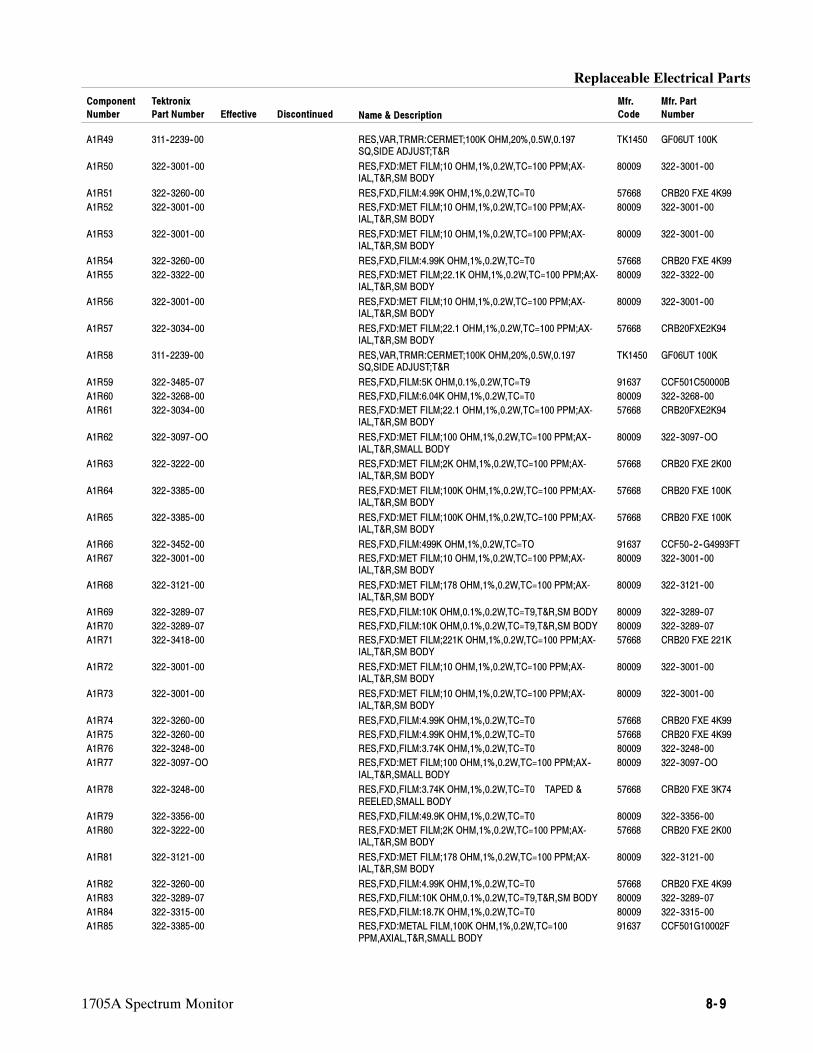
Replaceable Electrical Parts
1705A Spectrum Monitor 8- 9
Component
Number
Mfr. Part
Number
Mfr.
CodeName & DescriptionEffective Discontinued
Tektronix
Part Number
A1R49 311--2239--00 RES,VAR,TRMR:CERMET;100K OHM,20%,0.5W,0.197SQ,SIDE ADJUST;T&R
TK1450 GF06UT 100K
A1R50 322--3001--00 RES,FXD:MET FILM;10 OHM,1%,0.2W,TC=100 PPM;AX-IAL,T&R,SM BODY
80009 322--3001--00
A1R51 322--3260--00 RES,FXD,FILM:4.99K OHM,1%,0.2W,TC=T0 57668 CRB20 FXE 4K99
A1R52 322--3001--00 RES,FXD:MET FILM;10 OHM,1%,0.2W,TC=100 PPM;AX-IAL,T&R,SM BODY
80009 322--3001--00
A1R53 322--3001--00 RES,FXD:MET FILM;10 OHM,1%,0.2W,TC=100 PPM;AX-IAL,T&R,SM BODY
80009 322--3001--00
A1R54 322--3260--00 RES,FXD,FILM:4.99K OHM,1%,0.2W,TC=T0 57668 CRB20 FXE 4K99
A1R55 322--3322--00 RES,FXD:MET FILM;22.1K OHM,1%,0.2W,TC=100 PPM;AX-IAL,T&R,SM BODY
80009 322--3322--00
A1R56 322--3001--00 RES,FXD:MET FILM;10 OHM,1%,0.2W,TC=100 PPM;AX-IAL,T&R,SM BODY
80009 322--3001--00
A1R57 322--3034--00 RES,FXD:MET FILM;22.1 OHM,1%,0.2W,TC=100 PPM;AX-IAL,T&R,SM BODY
57668 CRB20FXE2K94
A1R58 311--2239--00 RES,VAR,TRMR:CERMET;100K OHM,20%,0.5W,0.197SQ,SIDE ADJUST;T&R
TK1450 GF06UT 100K
A1R59 322--3485--07 RES,FXD,FILM:5K OHM,0.1%,0.2W,TC=T9 91637 CCF501C50000B
A1R60 322--3268--00 RES,FXD,FILM:6.04K OHM,1%,0.2W,TC=T0 80009 322--3268--00
A1R61 322--3034--00 RES,FXD:MET FILM;22.1 OHM,1%,0.2W,TC=100 PPM;AX-IAL,T&R,SM BODY
57668 CRB20FXE2K94
A1R62 322--3097--OO RES,FXD:MET FILM;100 OHM,1%,0.2W,TC=100 PPM;AX--IAL,T&R,SMALL BODY
80009 322--3097--OO
A1R63 322--3222--00 RES,FXD:MET FILM;2K OHM,1%,0.2W,TC=100 PPM;AX-IAL,T&R,SM BODY
57668 CRB20 FXE 2K00
A1R64 322--3385--00 RES,FXD:MET FILM;100K OHM,1%,0.2W,TC=100 PPM;AX-IAL,T&R,SM BODY
57668 CRB20 FXE 100K
A1R65 322--3385--00 RES,FXD:MET FILM;100K OHM,1%,0.2W,TC=100 PPM;AX-IAL,T&R,SM BODY
57668 CRB20 FXE 100K
A1R66 322--3452--00 RES,FXD,FILM:499K OHM,1%,0.2W,TC=TO 91637 CCF50--2--G4993FT
A1R67 322--3001--00 RES,FXD:MET FILM;10 OHM,1%,0.2W,TC=100 PPM;AX-IAL,T&R,SM BODY
80009 322--3001--00
A1R68 322--3121--00 RES,FXD:MET FILM;178 OHM,1%,0.2W,TC=100 PPM;AX-IAL,T&R,SM BODY
80009 322--3121--00
A1R69 322--3289--07 RES,FXD,FILM:10K OHM,0.1%,0.2W,TC=T9,T&R,SM BODY 80009 322--3289--07
A1R70 322--3289--07 RES,FXD,FILM:10K OHM,0.1%,0.2W,TC=T9,T&R,SM BODY 80009 322--3289--07
A1R71 322--3418--00 RES,FXD:MET FILM;221K OHM,1%,0.2W,TC=100 PPM;AX-IAL,T&R,SM BODY
57668 CRB20 FXE 221K
A1R72 322--3001--00 RES,FXD:MET FILM;10 OHM,1%,0.2W,TC=100 PPM;AX-IAL,T&R,SM BODY
80009 322--3001--00
A1R73 322--3001--00 RES,FXD:MET FILM;10 OHM,1%,0.2W,TC=100 PPM;AX-IAL,T&R,SM BODY
80009 322--3001--00
A1R74 322--3260--00 RES,FXD,FILM:4.99K OHM,1%,0.2W,TC=T0 57668 CRB20 FXE 4K99
A1R75 322--3260--00 RES,FXD,FILM:4.99K OHM,1%,0.2W,TC=T0 57668 CRB20 FXE 4K99
A1R76 322--3248--00 RES,FXD,FILM:3.74K OHM,1%,0.2W,TC=T0 80009 322--3248--00
A1R77 322--3097--OO RES,FXD:MET FILM;100 OHM,1%,0.2W,TC=100 PPM;AX--IAL,T&R,SMALL BODY
80009 322--3097--OO
A1R78 322--3248--00 RES,FXD,FILM:3.74K OHM,1%,0.2W,TC=T0 TAPED &REELED,SMALL BODY
57668 CRB20 FXE 3K74
A1R79 322--3356--00 RES,FXD,FILM:49.9K OHM,1%,0.2W,TC=T0 80009 322--3356--00
A1R80 322--3222--00 RES,FXD:MET FILM;2K OHM,1%,0.2W,TC=100 PPM;AX-IAL,T&R,SM BODY
57668 CRB20 FXE 2K00
A1R81 322--3121--00 RES,FXD:MET FILM;178 OHM,1%,0.2W,TC=100 PPM;AX-IAL,T&R,SM BODY
80009 322--3121--00
A1R82 322--3260--00 RES,FXD,FILM:4.99K OHM,1%,0.2W,TC=T0 57668 CRB20 FXE 4K99
A1R83 322--3289--07 RES,FXD,FILM:10K OHM,0.1%,0.2W,TC=T9,T&R,SM BODY 80009 322--3289--07
A1R84 322--3315--00 RES,FXD,FILM:18.7K OHM,1%,0.2W,TC=T0 80009 322--3315--00
A1R85 322--3385--00 RES,FXD:METAL FILM,100K OHM,1%,0.2W,TC=100PPM,AXIAL,T&R,SMALL BODY
91637 CCF501G10002F
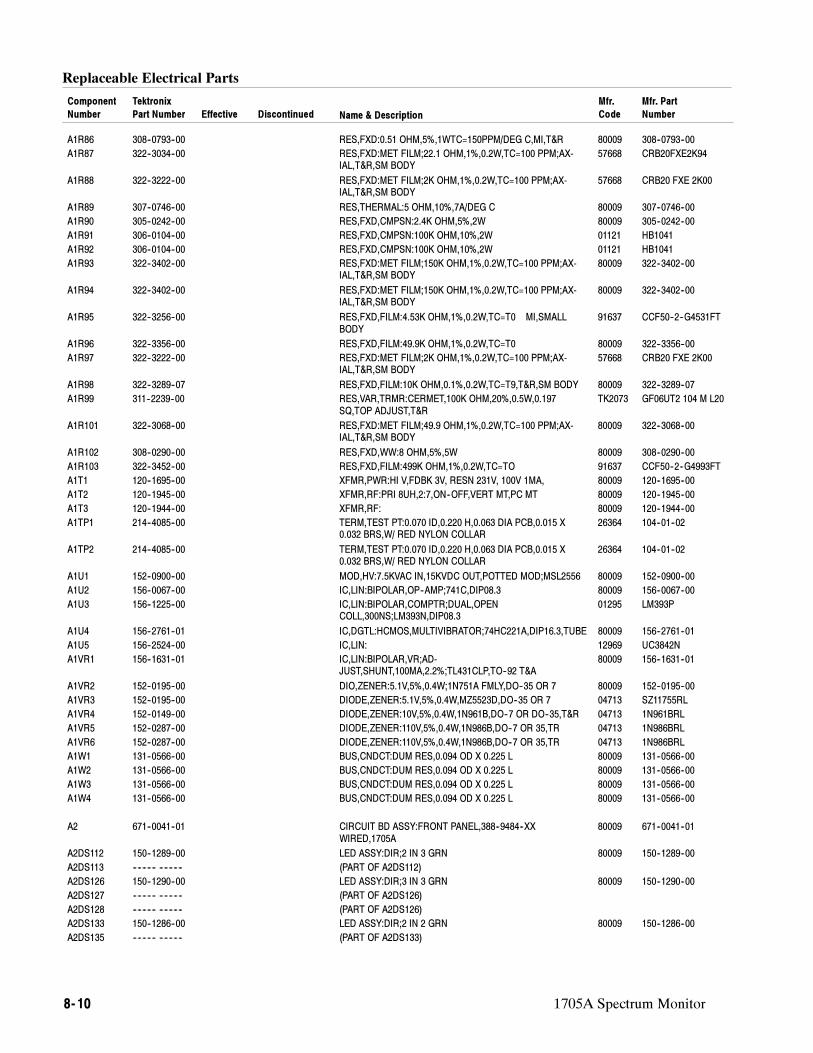
Replaceable Electrical Parts
8- 10 1705A Spectrum Monitor
Component
Number
Mfr. Part
Number
Mfr.
CodeName & DescriptionEffective Discontinued
Tektronix
Part Number
A1R86 308--0793--00 RES,FXD:0.51 OHM,5%,1WTC=150PPM/DEG C,MI,T&R 80009 308--0793--00
A1R87 322--3034--00 RES,FXD:MET FILM;22.1 OHM,1%,0.2W,TC=100 PPM;AX-IAL,T&R,SM BODY
57668 CRB20FXE2K94
A1R88 322--3222--00 RES,FXD:MET FILM;2K OHM,1%,0.2W,TC=100 PPM;AX-IAL,T&R,SM BODY
57668 CRB20 FXE 2K00
A1R89 307--0746--00 RES,THERMAL:5 OHM,10%,7A/DEG C 80009 307--0746--00
A1R90 305--0242--00 RES,FXD,CMPSN:2.4K OHM,5%,2W 80009 305--0242--00
A1R91 306--0104--00 RES,FXD,CMPSN:100K OHM,10%,2W 01121 HB1041
A1R92 306--0104--00 RES,FXD,CMPSN:100K OHM,10%,2W 01121 HB1041
A1R93 322--3402--00 RES,FXD:MET FILM;150K OHM,1%,0.2W,TC=100 PPM;AX-IAL,T&R,SM BODY
80009 322--3402--00
A1R94 322--3402--00 RES,FXD:MET FILM;150K OHM,1%,0.2W,TC=100 PPM;AX-IAL,T&R,SM BODY
80009 322--3402--00
A1R95 322--3256--00 RES,FXD,FILM:4.53K OHM,1%,0.2W,TC=T0 MI,SMALLBODY
91637 CCF50--2--G4531FT
A1R96 322--3356--00 RES,FXD,FILM:49.9K OHM,1%,0.2W,TC=T0 80009 322--3356--00
A1R97 322--3222--00 RES,FXD:MET FILM;2K OHM,1%,0.2W,TC=100 PPM;AX-IAL,T&R,SM BODY
57668 CRB20 FXE 2K00
A1R98 322--3289--07 RES,FXD,FILM:10K OHM,0.1%,0.2W,TC=T9,T&R,SM BODY 80009 322--3289--07
A1R99 311--2239--00 RES,VAR,TRMR:CERMET,100K OHM,20%,0.5W,0.197SQ,TOP ADJUST,T&R
TK2073 GF06UT2 104 M L20
A1R101 322--3068--00 RES,FXD:MET FILM;49.9 OHM,1%,0.2W,TC=100 PPM;AX-IAL,T&R,SM BODY
80009 322--3068--00
A1R102 308--0290--00 RES,FXD,WW:8 OHM,5%,5W 80009 308--0290--00
A1R103 322--3452--00 RES,FXD,FILM:499K OHM,1%,0.2W,TC=TO 91637 CCF50--2--G4993FT
A1T1 120--1695--00 XFMR,PWR:HI V,FDBK 3V, RESN 231V, 100V 1MA, 80009 120--1695--00
A1T2 120--1945--00 XFMR,RF:PRI 8UH,2:7,ON--OFF,VERT MT,PC MT 80009 120--1945--00
A1T3 120--1944--00 XFMR,RF: 80009 120--1944--00
A1TP1 214--4085--00 TERM,TEST PT:0.070 ID,0.220 H,0.063 DIA PCB,0.015 X0.032 BRS,W/ RED NYLON COLLAR
26364 104--01--02
A1TP2 214--4085--00 TERM,TEST PT:0.070 ID,0.220 H,0.063 DIA PCB,0.015 X0.032 BRS,W/ RED NYLON COLLAR
26364 104--01--02
A1U1 152--0900--00 MOD,HV:7.5KVAC IN,15KVDC OUT,POTTED MOD;MSL2556 80009 152--0900--00
A1U2 156--0067--00 IC,LIN:BIPOLAR,OP--AMP;741C,DIP08.3 80009 156--0067--00
A1U3 156--1225--00 IC,LIN:BIPOLAR,COMPTR;DUAL,OPENCOLL,300NS;LM393N,DIP08.3
01295 LM393P
A1U4 156--2761--01 IC,DGTL:HCMOS,MULTIVIBRATOR;74HC221A,DIP16.3,TUBE 80009 156--2761--01
A1U5 156--2524--00 IC,LIN: 12969 UC3842N
A1VR1 156--1631--01 IC,LIN:BIPOLAR,VR;AD-JUST,SHUNT,100MA,2.2%;TL431CLP,TO--92 T&A
80009 156--1631--01
A1VR2 152--0195--00 DIO,ZENER:5.1V,5%,0.4W;1N751A FMLY,DO--35 OR 7 80009 152--0195--00
A1VR3 152--0195--00 DIODE,ZENER:5.1V,5%,0.4W,MZ5523D,DO--35 OR 7 04713 SZ11755RL
A1VR4 152--0149--00 DIODE,ZENER:10V,5%,0.4W,1N961B,DO--7 OR DO--35,T&R 04713 1N961BRL
A1VR5 152--0287--00 DIODE,ZENER:110V,5%,0.4W,1N986B,DO--7 OR 35,TR 04713 1N986BRL
A1VR6 152--0287--00 DIODE,ZENER:110V,5%,0.4W,1N986B,DO--7 OR 35,TR 04713 1N986BRL
A1W1 131--0566--00 BUS,CNDCT:DUM RES,0.094 OD X 0.225 L 80009 131--0566--00
A1W2 131--0566--00 BUS,CNDCT:DUM RES,0.094 OD X 0.225 L 80009 131--0566--00
A1W3 131--0566--00 BUS,CNDCT:DUM RES,0.094 OD X 0.225 L 80009 131--0566--00
A1W4 131--0566--00 BUS,CNDCT:DUM RES,0.094 OD X 0.225 L 80009 131--0566--00
A2 671--0041--01 CIRCUIT BD ASSY:FRONT PANEL,388--9484--XXWIRED,1705A
80009 671--0041--01
A2DS112 150--1289--00 LED ASSY:DIR;2 IN 3 GRN 80009 150--1289--00
A2DS113 -- -- -- -- -- -- -- -- -- -- (PART OF A2DS112)
A2DS126 150--1290--00 LED ASSY:DIR;3 IN 3 GRN 80009 150--1290--00
A2DS127 -- -- -- -- -- -- -- -- -- -- (PART OF A2DS126)
A2DS128 -- -- -- -- -- -- -- -- -- -- (PART OF A2DS126)
A2DS133 150--1286--00 LED ASSY:DIR;2 IN 2 GRN 80009 150--1286--00
A2DS135 -- -- -- -- -- -- -- -- -- -- (PART OF A2DS133)
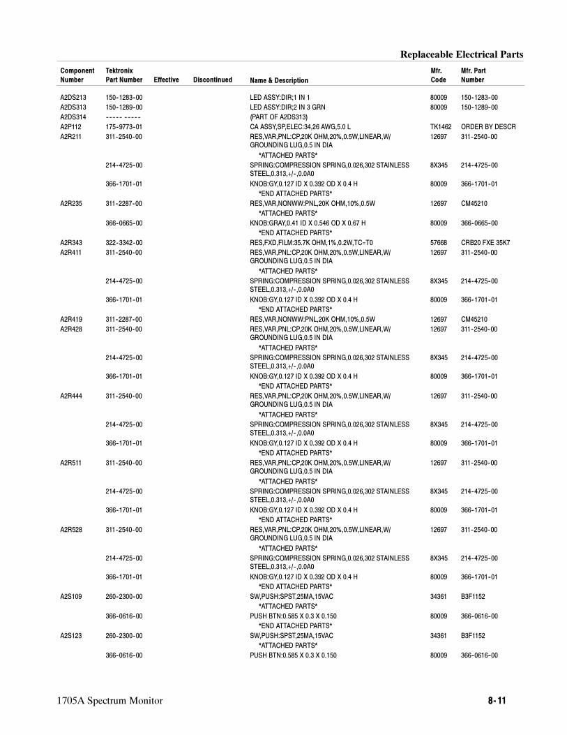
Replaceable Electrical Parts
1705A Spectrum Monitor 8- 11
Component
Number
Mfr. Part
Number
Mfr.
CodeName & DescriptionEffective Discontinued
Tektronix
Part Number
A2DS213 150--1283--00 LED ASSY:DIR;1 IN 1 80009 150--1283--00
A2DS313 150--1289--00 LED ASSY:DIR;2 IN 3 GRN 80009 150--1289--00
A2DS314 -- -- -- -- -- -- -- -- -- -- (PART OF A2DS313)
A2P112 175--9773--01 CA ASSY,SP,ELEC:34,26 AWG,5.0 L TK1462 ORDER BY DESCR
A2R211 311--2540--00 RES,VAR,PNL:CP,20K OHM,20%,0.5W,LINEAR,W/GROUNDING LUG,0.5 IN DIA
12697 311--2540--00
*ATTACHED PARTS*
214--4725--00 SPRING:COMPRESSION SPRING,0.026,302 STAINLESSSTEEL,0.313,+/--,0.0A0
8X345 214--4725--00
366--1701--01 KNOB:GY,0.127 ID X 0.392 OD X 0.4 H 80009 366--1701--01
*END ATTACHED PARTS*
A2R235 311--2287--00 RES,VAR,NONWW:PNL,20K OHM,10%,0.5W 12697 CM45210
*ATTACHED PARTS*
366--0665--00 KNOB:GRAY,0.41 ID X 0.546 OD X 0.67 H 80009 366--0665--00
*END ATTACHED PARTS*
A2R343 322--3342--00 RES,FXD,FILM:35.7K OHM,1%,0.2W,TC=T0 57668 CRB20 FXE 35K7
A2R411 311--2540--00 RES,VAR,PNL:CP,20K OHM,20%,0.5W,LINEAR,W/GROUNDING LUG,0.5 IN DIA
12697 311--2540--00
*ATTACHED PARTS*
214--4725--00 SPRING:COMPRESSION SPRING,0.026,302 STAINLESSSTEEL,0.313,+/--,0.0A0
8X345 214--4725--00
366--1701--01 KNOB:GY,0.127 ID X 0.392 OD X 0.4 H 80009 366--1701--01
*END ATTACHED PARTS*
A2R419 311--2287--00 RES,VAR,NONWW:PNL,20K OHM,10%,0.5W 12697 CM45210
A2R428 311--2540--00 RES,VAR,PNL:CP,20K OHM,20%,0.5W,LINEAR,W/GROUNDING LUG,0.5 IN DIA
12697 311--2540--00
*ATTACHED PARTS*
214--4725--00 SPRING:COMPRESSION SPRING,0.026,302 STAINLESSSTEEL,0.313,+/--,0.0A0
8X345 214--4725--00
366--1701--01 KNOB:GY,0.127 ID X 0.392 OD X 0.4 H 80009 366--1701--01
*END ATTACHED PARTS*
A2R444 311--2540--00 RES,VAR,PNL:CP,20K OHM,20%,0.5W,LINEAR,W/GROUNDING LUG,0.5 IN DIA
12697 311--2540--00
*ATTACHED PARTS*
214--4725--00 SPRING:COMPRESSION SPRING,0.026,302 STAINLESSSTEEL,0.313,+/--,0.0A0
8X345 214--4725--00
366--1701--01 KNOB:GY,0.127 ID X 0.392 OD X 0.4 H 80009 366--1701--01
*END ATTACHED PARTS*
A2R511 311--2540--00 RES,VAR,PNL:CP,20K OHM,20%,0.5W,LINEAR,W/GROUNDING LUG,0.5 IN DIA
12697 311--2540--00
*ATTACHED PARTS*
214--4725--00 SPRING:COMPRESSION SPRING,0.026,302 STAINLESSSTEEL,0.313,+/--,0.0A0
8X345 214--4725--00
366--1701--01 KNOB:GY,0.127 ID X 0.392 OD X 0.4 H 80009 366--1701--01
*END ATTACHED PARTS*
A2R528 311--2540--00 RES,VAR,PNL:CP,20K OHM,20%,0.5W,LINEAR,W/GROUNDING LUG,0.5 IN DIA
12697 311--2540--00
*ATTACHED PARTS*
214--4725--00 SPRING:COMPRESSION SPRING,0.026,302 STAINLESSSTEEL,0.313,+/--,0.0A0
8X345 214--4725--00
366--1701--01 KNOB:GY,0.127 ID X 0.392 OD X 0.4 H 80009 366--1701--01
*END ATTACHED PARTS*
A2S109 260--2300--00 SW,PUSH:SPST,25MA,15VAC 34361 B3F1152
*ATTACHED PARTS*
366--0616--00 PUSH BTN:0.585 X 0.3 X 0.150 80009 366--0616--00
*END ATTACHED PARTS*
A2S123 260--2300--00 SW,PUSH:SPST,25MA,15VAC 34361 B3F1152
*ATTACHED PARTS*
366--0616--00 PUSH BTN:0.585 X 0.3 X 0.150 80009 366--0616--00
Replaceable Electrical Parts
8- 12 1705A Spectrum Monitor
Component
Number
Mfr. Part
Number
Mfr.
CodeName & DescriptionEffective Discontinued
Tektronix
Part Number
*END ATTACHED PARTS*
A2S139 260--2300--00 SW,PUSH:SPST,25MA,15VAC 34361 B3F1152
*ATTACHED PARTS*
366--0616--00 PUSH BTN:0.585 X 0.3 X 0.150 80009 366--0616--00
*END ATTACHED PARTS*
A2S311 260--2300--00 SW,PUSH:SPST,25MA,15VAC 34361 B3F1152
*ATTACHED PARTS*
366--0616--00 PUSH BTN:0.585 X 0.3 X 0.150 80009 366--0616--00
*END ATTACHED PARTS*
A2S345 260--2300--00 SW,PUSH:SPST,25MA,15VAC 34361 B3F1152
*ATTACHED PARTS*
366--0616--00 PUSH BTN:0.585 X 0.3 X 0.150 80009 366--0616--00
*END ATTACHED PARTS*
A3 672--1373--05 CIRCUIT BD ASSY:MAIN BOARD ASSY,1705A 80009 672--1373--05
A3 672--1373--08 8--15--2003 CIRCUIT BD ASSY:MAIN BOARD ASSY,1705A 80009 672--1373--08
*ATTACHED PARTS*
131--3717--00 BUS,CNDCT: TK1884 SM2098
202--0196--01 SHIELD,ELEC:1.29 SQ X 0.675,AL 02875 HU4430--0.953--AL
337--0607--00 PLATE,ELEC SHLD:CIRCUIT BOARD 80009 337--0607--00
337--2804--00 SHIELD,ELEC:CIRCUIT BOARD 80009 337--2804--00
337--3834--00 SHIELD,ELEC:1705A,BRS 80009 337--3834--00
337--3923--00 SHIELD,ELEC:TOP,1705A 80009 337--3923--00
337--3924--00 SHIELD,ELEC:FENCE,1705A 80009 337--3924--00
337--3925--00 SHIELD,ELEC:BOTTOM,1705A 80009 337--3925--00
*END ATTACHED PARTS*
A3C1 290--0748--00 CAP,FXD,ELCTLT:10UF,+50--20%,25WVDC 24165 501D106F063LL4
A3C2 281--0819--00 CAP,FXD,CER:MLC;33 PF,5%,50V,0.100 X 0.170;AXIAL,MI 04222 SA102A330JAA
A3C3 281--0819--00 CAP,FXD,CER:MLC;33 PF,5%,50V,0.100 X 0.170;AXIAL,MI 04222 SA102A330JAA
A3C4 281--0775--01 CAP,FXD,CER:MCL;0.1UF,20%,50V,Z5U,0.170 X 0.100;AXIAL 04222 SA105E104MAA
A3C5 290--1296--00 CAP,FXD,ALUM:100UF,20%,25V,8 X 9MM;RDL,105DEG,BULK
80009 290--1296--00
A3C6 281--0775--01 CAP,FXD,CER:MCL;0.1UF,20%,50V,Z5U,0.170 X 0.100;AXIAL 04222 SA105E104MAA
A3C7 281--0775--01 CAP,FXD,CER:MCL;0.1UF,20%,50V,Z5U,0.170 X 0.100;AXIAL 04222 SA105E104MAA
A3C8 281--0775--01 CAP,FXD,CER:MCL;0.1UF,20%,50V,Z5U,0.170 X 0.100;AXIAL 04222 SA105E104MAA
A3C10 281--0775--01 CAP,FXD,CER:MCL;0.1UF,20%,50V,Z5U,0.170 X 0.100;AXIAL 04222 SA105E104MAA
A3C11 281--0775--01 CAP,FXD,CER:MCL;0.1UF,20%,50V,Z5U,0.170 X 0.100;AXIAL 04222 SA105E104MAA
A3C12 281--0775--01 CAP,FXD,CER:MCL;0.1UF,20%,50V,Z5U,0.170 X 0.100;AXIAL 04222 SA105E104MAA
A3C13 290--1295--00 CAP,FXD,ALUM:10UF,20%,16V,5 X 9 MM;RDL,105 DEG,BULK 80009 290--1295--00
A3C14 281--0775--01 CAP,FXD,CER:MCL;0.1UF,20%,50V,Z5U,0.170 X 0.100;AXIAL 04222 SA105E104MAA
A3C15 281--0775--01 CAP,FXD,CER:MCL;0.1UF,20%,50V,Z5U,0.170 X 0.100;AXIAL 04222 SA105E104MAA
A3C16 281--0775--01 CAP,FXD,CER:MCL;0.1UF,20%,50V,Z5U,0.170 X 0.100;AXIAL 04222 SA105E104MAA
A3C17 281--0775--01 CAP,FXD,CER:MCL;0.1UF,20%,50V,Z5U,0.170 X 0.100;AXIAL 04222 SA105E104MAA
A3C18 281--0775--01 CAP,FXD,CER:MCL;0.1UF,20%,50V,Z5U,0.170 X 0.100;AXIAL 04222 SA105E104MAA
A3C19 281--0775--01 CAP,FXD,CER:MCL;0.1UF,20%,50V,Z5U,0.170 X 0.100;AXIAL 04222 SA105E104MAA
A3C20 281--0775--01 CAP,FXD,CER:MCL;0.1UF,20%,50V,Z5U,0.170 X 0.100;AXIAL 04222 SA105E104MAA
A3C21 281--0775--01 CAP,FXD,CER:MCL;0.1UF,20%,50V,Z5U,0.170 X 0.100;AXIAL 04222 SA105E104MAA
A3C22 281--0775--01 CAP,FXD,CER:MCL;0.1UF,20%,50V,Z5U,0.170 X 0.100;AXIAL 04222 SA105E104MAA
A3C24 290--1295--00 CAP,FXD,ALUM:10UF,20%,16V,5 X 9 MM;RDL,105 DEG,BULK 80009 290--1295--00
A3C25 281--0812--00 CAP,FXD,CER:MLC;1000PF,10%,100V,0.100 X 0.170;AX-IAL,MI
04222 SA101C102KAA
A3C26 290--1295--00 CAP,FXD,ALUM:10UF,20%,16V,5 X 9 MM;RDL,105 DEG,BULK 80009 290--1295--00
A3C28 281--0775--01 CAP,FXD,CER:MCL;0.1UF,20%,50V,Z5U,0.170 X 0.100;AXIAL 04222 SA105E104MAA
A3C29 281--0775--01 CAP,FXD,CER:MCL;0.1UF,20%,50V,Z5U,0.170 X 0.100;AXIAL 04222 SA105E104MAA
A3C30 281--0775--01 CAP,FXD,CER:MCL;0.1UF,20%,50V,Z5U,0.170 X 0.100;AXIAL 04222 SA105E104MAA
A3C31 281--0773--00 CAP,FXD,CER:MLC;0.01UF,10%,100V,SAF,0.100 X 0.170;AX-IAL,MI
80009 281--0773--00
A3C32 281--0772--00 CAP,FXD,CER:MLC;4700PF,10%,100V,0.100 X 0.170;AX-IAL,MI
04222 SA101C472KAA
Replaceable Electrical Parts
1705A Spectrum Monitor 8- 13
Component
Number
Mfr. Part
Number
Mfr.
CodeName & DescriptionEffective Discontinued
Tektronix
Part Number
A3C33 281--0773--00 CAP,FXD,CER:MLC;0.01UF,10%,100V,SAF,0.100 X 0.170;AX-IAL,MI
80009 281--0773--00
A3C34 281--0773--00 CAP,FXD,CER:MLC;0.01UF,10%,100V,SAF,0.100 X 0.170;AX-IAL,MI
80009 281--0773--00
A3C35 281--0773--00 CAP,FXD,CER:MLC;0.01UF,10%,100V,SAF,0.100 X 0.170;AX-IAL,MI
80009 281--0773--00
A3C36 290--0920--00 CAP,FXD,ELCTLT:33UF,+50--20%,35WVDC 55680 UVX1H330MAA
A3C37 281--0775--01 CAP,FXD,CER:MCL;0.1UF,20%,50V,Z5U,0.170 X 0.100;AXIAL 04222 SA105E104MAA
A3C38 281--0775--01 CAP,FXD,CER:MCL;0.1UF,20%,50V,Z5U,0.170 X 0.100;AXIAL 04222 SA105E104MAA
A3C39 281--0812--00 CAP,FXD,CER:MLC;1000PF,10%,100V,0.100 X 0.170;AX-IAL,MI
04222 SA101C102KAA
A3C40 281--0775--01 CAP,FXD,CER:MCL;0.1UF,20%,50V,Z5U,0.170 X 0.100;AXIAL 04222 SA105E104MAA
A3C41 281--0763--00 CAP,FXD,CER:MLC;47PF,10%,100V,0.100 X 0.170;AXIAL,MI 04222 SA102A470KAA
A3C42 281--0797--00 CAP,FXD,CER:MLC;15PF,10%,100V,SAF ,0.100 X 0.170;AX-IAL,MI
80009 281--0797--00
A3C43 281--0823--00 CAP,FXD,CER DI:470PF,10%,50V 04222 SA101A471KAA
A3C46 281--0775--01 CAP,FXD,CER:MCL;0.1UF,20%,50V,Z5U,0.170 X 0.100;AXIAL 04222 SA105E104MAA
A3C47 281--0775--01 CAP,FXD,CER:MCL;0.1UF,20%,50V,Z5U,0.170 X 0.100;AXIAL 04222 SA105E104MAA
A3C48 281--0775--01 CAP,FXD,CER:MCL;0.1UF,20%,50V,Z5U,0.170 X 0.100;AXIAL 04222 SA105E104MAA
A3C49 281--0775--01 CAP,FXD,CER:MCL;0.1UF,20%,50V,Z5U,0.170 X 0.100;AXIAL 04222 SA105E104MAA
A3C50 281--0538--00 CAP,FXD,CER:MLC;1PF,20%,500V,O.170 X 0.220;AXIAL 80009 281--0538--00
A3C51 281--0812--00 CAP,FXD,CER:MLC;1000PF,10%,100V,0.100 X 0.170;AX-IAL,MI
04222 SA101C102KAA
A3C52 281--0167--00 CAP,VAR,CER DI:9--45PF,200V 33095 53--717--001 D9--45
A3C53 281--0775--01 CAP,FXD,CER:MCL;0.1UF,20%,50V,Z5U,0.170 X 0.100;AXIAL 04222 SA105E104MAA
A3C54 281--0812--00 CAP,FXD,CER:MLC;1000PF,10%,100V,0.100 X 0.170;AX-IAL,MI
04222 SA101C102KAA
A3C55 281--0178--00 CAP,VAR,PLSTC:1--3.5PF,500V 80009 281--0178--00
A3C56 281--0775--01 CAP,FXD,CER:MCL;0.1UF,20%,50V,Z5U,0.170 X 0.100;AXIAL 04222 SA105E104MAA
A3C57 281--0775--01 CAP,FXD,CER:MCL;0.1UF,20%,50V,Z5U,0.170 X 0.100;AXIAL 04222 SA105E104MAA
A3C58 281--0773--00 CAP,FXD,CER:MLC;0.01UF,10%,100V,SAF,0.100 X 0.170;AX-IAL,MI
80009 281--0773--00
A3C59 281--0823--00 CAP,FXD,CER DI:470PF,10%,50V 04222 SA101A471KAA
A3C60 281--0809--00 CAP,FXD,CER:MLC;200 PF,5%,100V,0.100 X 0.170;AXIAL,MI 04222 SA101A201JAA
A3C61 290--0920--00 CAP,FXD,ELCTLT:33UF,+50--20%,35WVDC 55680 UVX1H330MAA
A3C62 281--0123--00 CAP,VAR,CER DI:5--25PF,100V 59660 518--000A5--25
A3C63 281--0809--00 CAP,FXD,CER:MLC;200 PF,5%,100V,0.100 X 0.170;AXIAL,MI 04222 SA101A201JAA
A3C64 281--0167--00 CAP,VAR,CER DI:9--45PF,200V 33095 53--717--001 D9--45
A3C65 281--0775--01 CAP,FXD,CER:MCL;0.1UF,20%,50V,Z5U,0.170 X 0.100;AXIAL 04222 SA105E104MAA
A3C68 281--0773--00 CAP,FXD,CER:MLC;0.01UF,10%,100V,SAF,0.100 X 0.170;AX-IAL,MI
80009 281--0773--00
A3C69 281--0168--00 CAP,VAR,AIR DI:1.3--5.4PF,250V 80009 281--0168--00
A3C70 281--0773--00 CAP,FXD,CER:MLC;0.01UF,10%,100V,SAF,0.100 X 0.170;AX-IAL,MI
80009 281--0773--00
A3C71 281--0820--00 CAP,FXD,CER:MLC;680 PF,10%,50V,0.100 X 0.170;AXIAL,MI 04222 SA101C681KAA
A3C72 281--0820--00 CAP,FXD,CER:MLC;680 PF,10%,50V,0.100 X 0.170;AXIAL,MI 04222 SA101C681KAA
A3C73 281--0773--00 CAP,FXD,CER:MLC;0.01UF,10%,100V,SAF,0.100 X 0.170;AX-IAL,MI
80009 281--0773--00
A3C74 281--0775--01 CAP,FXD,CER:MCL;0.1UF,20%,50V,Z5U,0.170 X 0.100;AXIAL 04222 SA105E104MAA
A3C77 281--0775--01 CAP,FXD,CER:MCL;0.1UF,20%,50V,Z5U,0.170 X 0.100;AXIAL 04222 SA105E104MAA
A3C78 281--0812--00 CAP,FXD,CER:MLC;1000PF,10%,100V,0.100 X 0.170;AX-IAL,MI
04222 SA101C102KAA
A3C79 281--0775--01 CAP,FXD,CER:MCL;0.1UF,20%,50V,Z5U,0.170 X 0.100;AXIAL 04222 SA105E104MAA
A3C80 281--0775--01 CAP,FXD,CER:MCL;0.1UF,20%,50V,Z5U,0.170 X 0.100;AXIAL 04222 SA105E104MAA
A3C81 281--0773--00 CAP,FXD,CER:MLC;0.01UF,10%,100V,SAF,0.100 X 0.170;AX-IAL,MI
80009 281--0773--00
A3C82 281--0813--00 CAP,FXD,CER:MLC;0.047UF,20%,50V,0.100 X 0.170;AXIAL,MI 04222 SA105E473MAA
A3C83 281--0813--00 CAP,FXD,CER:MLC;0.047UF,20%,50V,0.100 X 0.170;AXIAL,MI 04222 SA105E473MAA
Replaceable Electrical Parts
8- 14 1705A Spectrum Monitor
Component
Number
Mfr. Part
Number
Mfr.
CodeName & DescriptionEffective Discontinued
Tektronix
Part Number
A3C84 281--0812--00 CAP,FXD,CER:MLC;1000PF,10%,100V,0.100 X 0.170;AX-IAL,MI
04222 SA101C102KAA
A3C85 281--0812--00 CAP,FXD,CER:MLC;1000PF,10%,100V,0.100 X 0.170;AX-IAL,MI
04222 SA101C102KAA
A3C87 283--0599--02 CAP,FXD,MICA DI:98PF,5%,500V 09023 CDA10FD980J03
A3C88 281--0809--00 CAP,FXD,CER:MLC;200 PF,5%,100V,0.100 X 0.170;AXIAL,MI 04222 SA101A201JAA
A3C89 281--0775--01 CAP,FXD,CER:MCL;0.1UF,20%,50V,Z5U,0.170 X 0.100;AXIAL 04222 SA105E104MAA
A3C90 281--0773--00 CAP,FXD,CER:MLC;0.01UF,10%,100V,SAF,0.100 X 0.170;AX-IAL,MI
80009 281--0773--00
A3C91 290--0920--00 CAP,FXD,ELCTLT:33UF,+50--20%,35WVDC 55680 UVX1H330MAA
A3C92 281--0864--00 CAP,FXD,CER:MLC;430PF,5%,100V,0.100 X 0.170;AXIAL,MI 04222 SA101A431JAA
A3C93 281--0765--00 CAP,FXD,CER DI:100PF,5%,100V 04222 SA102A101JAA
A3C100 281--0812--00 CAP,FXD,CER:MLC;1000PF,10%,100V,0.100 X 0.170;AX-IAL,MI
04222 SA101C102KAA
A3C101 281--0904--00 CAP,FXD,CER:MLC;12PF,10%,100V,0.100 X 0.170;AXIAL,MI 80009 281--0904--00
A3C102 281--0775--01 CAP,FXD,CER:MCL;0.1UF,20%,50V,Z5U,0.170 X 0.100;AXIAL 04222 SA105E104MAA
A3CR1 152--0141--02 DIO,SIG:ULTRAFAST;40V,150MA,4NS,2PF;1N4152,DO--35,T&R
80009 152--0141--02
A3CR2 152--0501--01 DIO,SIG:FAST RCVRY;70V,200MA,100NS,COM--ANODE;MSD6150,TO--92,TR
80009 152--0501--01
A3CR3 152--0141--02 DIO,SIG:ULTRAFAST;40V,150MA,4NS,2PF;1N4152,DO--35,T&R
80009 152--0141--02
A3CR4 152--0141--02 DIO,SIG:ULTRAFAST;40V,150MA,4NS,2PF;1N4152,DO--35,T&R
80009 152--0141--02
A3CR5 152--0141--02 DIO,SIG:ULTRAFAST;40V,150MA,4NS,2PF;1N4152,DO--35,T&R
80009 152--0141--02
A3CR6 152--0141--02 DIO,SIG:ULTRAFAST;40V,150MA,4NS,2PF;1N4152,DO--35,T&R
80009 152--0141--02
A3CR7 152--0141--02 DIO,SIG:ULTRAFAST;40V,150MA,4NS,2PF;1N4152,DO--35,T&R
80009 152--0141--02
A3CR8 152--0141--02 DIO,SIG:ULTRAFAST;40V,150MA,4NS,2PF;1N4152,DO--35,T&R
80009 152--0141--02
A3CR9 152--0066--00 DIO,RECT:400V,1A,IFSM=30A,1.2VF,2US;GP10G/1N5060,T&R,SAF CONT
05828 GP10G--020
A3CR10 152--0066--00 DIO,RECT:400V,1A,IFSM=30A,1.2VF,2US;GP10G/1N5060,T&R,SAF CONT
05828 GP10G--020
A3CR11 152--0141--02 DIO,SIG:ULTRAFAST;40V,150MA,4NS,2PF;1N4152,DO--35,T&R
80009 152--0141--02
A3CR12 152--0141--02 DIO,SIG:ULTRAFAST;40V,150MA,4NS,2PF;1N4152,DO--35,T&R
80009 152--0141--02
A3CR13 152--0141--02 DIO,SIG:ULTRAFAST;40V,150MA,4NS,2PF;1N4152,DO--35,T&R
80009 152--0141--02
A3CR14 152--0141--02 DIO,SIG:ULTRAFAST;40V,150MA,4NS,2PF;1N4152,DO--35,T&R
80009 152--0141--02
A3CR15 152--0141--02 DIO,SIG:ULTRAFAST;40V,150MA,4NS,2PF;1N4152,DO--35,T&R
80009 152--0141--02
A3CR16 152--0141--02 DIO,SIG:ULTRAFAST;40V,150MA,4NS,2PF;1N4152,DO--35,T&R
80009 152--0141--02
A3CR17 152--0066--00 DIO,RECT:400V,1A,IFSM=30A,1.2VF,2US;GP10G/1N5060,T&R,SAF CONT
05828 GP10G--020
A3CR18 152--0066--00 DIO,RECT:400V,1A,IFSM=30A,1.2VF,2US;GP10G/1N5060,T&R,SAF CONT
05828 GP10G--020
A3CR19 152--0141--02 DIO,SIG:ULTRAFAST;40V,150MA,4NS,2PF;1N4152,DO--35,T&R
80009 152--0141--02
A3CR20 152--0141--02 DIO,SIG:ULTRAFAST;40V,150MA,4NS,2PF;1N4152,DO--35,T&R
80009 152--0141--02
A3CR21 152--0141--02 DIO,SIG:ULTRAFAST;40V,150MA,4NS,2PF;1N4152,DO--35,T&R
80009 152--0141--02
A3CR22 152--0141--02 DIO,SIG:ULTRAFAST;40V,150MA,4NS,2PF;1N4152,DO--35,T&R
80009 152--0141--02
Replaceable Electrical Parts
1705A Spectrum Monitor 8- 15
Component
Number
Mfr. Part
Number
Mfr.
CodeName & DescriptionEffective Discontinued
Tektronix
Part Number
A3CR23 152--0141--02 DIO,SIG:ULTRAFAST;40V,150MA,4NS,2PF;1N4152,DO--35,T&R
80009 152--0141--02
A3CR24 152--0141--02 DIO,SIG:ULTRAFAST;40V,150MA,4NS,2PF;1N4152,DO--35,T&R
80009 152--0141--02
A3CR25 152--0141--02 DIO,SIG:ULTRAFAST;40V,150MA,4NS,2PF;1N4152,DO--35,T&R
80009 152--0141--02
A3CR26 152--0141--02 DIO,SIG:ULTRAFAST;40V,150MA,4NS,2PF;1N4152,DO--35,T&R
80009 152--0141--02
A3CR27 152--0141--02 DIO,SIG:ULTRAFAST;40V,150MA,4NS,2PF;1N4152,DO--35,T&R
80009 152--0141--02
A3CR28 152--0141--02 DIO,SIG:ULTRAFAST;40V,150MA,4NS,2PF;1N4152,DO--35,T&R
80009 152--0141--02
A3CR29 152--0141--02 DIO,SIG:ULTRAFAST;40V,150MA,4NS,2PF;1N4152,DO--35,T&R
80009 152--0141--02
A3CR30 152--0141--02 DIO,SIG:ULTRAFAST;40V,150MA,4NS,2PF;1N4152,DO--35,T&R
80009 152--0141--02
A3CR31 152--0141--02 DIO,SIG:ULTRAFAST;40V,150MA,4NS,2PF;1N4152,DO--35,T&R
80009 152--0141--02
A3CR32 152--0141--02 DIO,SIG:ULTRAFAST;40V,150MA,4NS,2PF;1N4152,DO--35,T&R
80009 152--0141--02
A3FL1 119--4325--00 FLTR,BANDPASS: 80009 119--4325--00
A3FL2 119--4324--00 FLTR,BANDPASS: 80009 119--4324--00
A3FL3 119--2590--00 FLTR,RFI:10.7MHZ 80009 119--2590--00
A3FL4 119--2590--00 FLTR,RFI:10.7MHZ 80009 119--2590--00
A3J1 131--3571--00 CONN,HDR: 80009 131--3571--00
A3J2 131--4752--00 CONN,HDR:PCB;MALE,45 DEG,1 X 2,0.1 CTR,0.240 MLG X0.110 TAIL,30 GLD
80009 131--4752--00
A3J3 131--4752--00 CONN,HDR:PCB;MALE,45 DEG,1 X 2,0.1 CTR,0.240 MLG X0.110 TAIL,30 GLD
80009 131--4752--00
A3J4 175--9797--00 CA ASSY,SP:FLAT FLEX;FLX,10,27 AWG,2.5 L,1X10,BOX XSTR,SLDR TAB,CONN NON PLZ
00779 487729--1
A3J5 131--2919--01 CONN,HDR:PCB;MALE,STR,1 X 4,0.1 CTR,0.235 MLG X0.112 TAIL,30 GLD,0.035 DIA PCB
80009 131--2919--01
A3J6 131--2919--01 CONN,HDR:PCB;MALE,STR,1 X 4,0.1 CTR,0.235 MLG X0.112 TAIL,30 GLD,0.035 DIA PCB
80009 131--2919--01
A3J9 131--0391--00 CONN,RF JACK: 80009 131--0391--00
A3J10 131--2919--01 CONN,HDR:PCB;MALE,STR,1 X 4,0.1 CTR,0.235 MLG X0.112 TAIL,30 GLD,0.035 DIA PCB
80009 131--2919--01
A3J11 131--0391--00 CONN,RF JACK: 80009 131--0391--00
A3J100 131--4752--00 CONN,HDR:PCB;MALE,45 DEG,1 X 2,0.1 CTR,0.240 MLG X0.110 TAIL,30 GLD
80009 131--4752--00
A3J101 131--4752--00 CONN,HDR:PCB;MALE,45 DEG,1 X 2,0.1 CTR,0.240 MLG X0.110 TAIL,30 GLD
80009 131--4752--00
A3J200 131--4794--00 CONN,HDR:PCB;MALE,STR,1 X 2,0.1 CTR,0.235 MLG X0.112 TAIL,30 GLD,0.035 DIA PCB
80009 131--4794--00
A3J201 131--4794--00 CONN,HDR:PCB;MALE,STR,1 X 2,0.1 CTR,0.235 MLG X0.112 TAIL,30 GLD,0.035 DIA PCB
80009 131--4794--00
A3J202 131--4794--00 CONN,HDR:PCB;MALE,STR,1 X 2,0.1 CTR,0.235 MLG X0.112 TAIL,30 GLD,0.035 DIA PCB
80009 131--4794--00
A3J203 131--4794--00 CONN,HDR:PCB;MALE,STR,1 X 2,0.1 CTR,0.235 MLG X0.112 TAIL,30 GLD,0.035 DIA PCB
80009 131--4794--00
A3J300 131--4752--00 CONN,HDR:PCB;MALE,45 DEG,1 X 2,0.1 CTR,0.240 MLG X0.110 TAIL,30 GLD
80009 131--4752--00
A3L1 120--0382--00 COIL,RF:210UH,+28%--43%,14 TURNS,TEST COND. 10 KHZ,0.115 MA
TK1345 120--0382--00
A3L2 120--0382--00 COIL,RF:210UH,+28%--43%,14 TURNS,TEST COND. 10 KHZ,0.115 MA
TK1345 120--0382--00
A3L3 120--0382--00 COIL,RF:210UH,+28%--43%,14 TURNS,TEST COND. 10 KHZ,0.115 MA
TK1345 120--0382--00
A3L4 114--0475--00 COIL,RF: 80009 114--0475--00
A3L5 108--0826--00 COIL,RF: 80009 108--0826--00
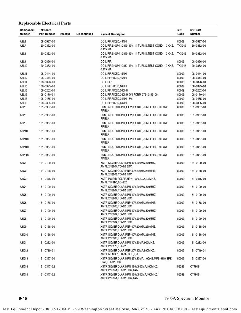
Replaceable Electrical Parts
8- 16 1705A Spectrum Monitor
Component
Number
Mfr. Part
Number
Mfr.
CodeName & DescriptionEffective Discontinued
Tektronix
Part Number
A3L6 108--0987--00 COIL,RF:FIXED,45NH 80009 108--0987--00
A3L7 120--0382--00 COIL,RF:210UH,+28%--43%,14 TURNS,TEST COND. 10 KHZ,0.115 MA
TK1345 120--0382--00
A3L8 120--0382--00 COIL,RF:210UH,+28%--43%,14 TURNS,TEST COND. 10 KHZ,0.115 MA
TK1345 120--0382--00
A3L9 108--0826--00 COIL,RF: 80009 108--0826--00
A3L10 120--0382--00 COIL,RF:210UH,+28%--43%,14 TURNS,TEST COND. 10 KHZ,0.115 MA
TK1345 120--0382--00
A3L11 108--0444--00 COIL,RF:FIXED,15NH 80009 108--0444--00
A3L12 108--0444--00 COIL,RF:FIXED,15NH 80009 108--0444--00
A3L14 108--0826--00 COIL,RF: 80009 108--0826--00
A3L15 108--0395--00 COIL,RF:FIXED,64UH 80009 108--0395--00
A3L16 108--0262--00 COIL,RF:FIXED,505NH 80009 108--0262--00
A3L17 108--0170--01 COIL,RF:FIXED,360NH ON FORM 276--0153--00 80009 108--0170--01
A3L18 108--0455--00 COIL,RF:FIXED,24NH,15% 80009 108--0455--00
A3L19 108--0395--00 COIL,RF:FIXED,64UH 80009 108--0395--00
A3P3 131--3957--00 BUS,CNDCT:SHUNT,1 X 2,0.1 CTR,JUMPER,0.2 H,LOWPF,BLK
80009 131--3957--00
A3P5 131--3957--00 BUS,CNDCT:SHUNT,1 X 2,0.1 CTR,JUMPER,0.2 H,LOWPF,BLK
80009 131--3957--00
A3P6 131--3957--00 BUS,CNDCT:SHUNT,1 X 2,0.1 CTR,JUMPER,0.2 H,LOWPF,BLK
80009 131--3957--00
A3P10 131--3957--00 BUS,CNDCT:SHUNT,1 X 2,0.1 CTR,JUMPER,0.2 H,LOWPF,BLK
80009 131--3957--00
A3P100 131--3957--00 BUS,CNDCT:SHUNT,1 X 2,0.1 CTR,JUMPER,0.2 H,LOWPF,BLK
80009 131--3957--00
A3P101 131--3957--00 BUS,CNDCT:SHUNT,1 X 2,0.1 CTR,JUMPER,0.2 H,LOWPF,BLK
80009 131--3957--00
A3P300 131--3957--00 BUS,CNDCT:SHUNT,1 X 2,0.1 CTR,JUMPER,0.2 H,LOWPF,BLK
80009 131--3957--00
A3Q1 151--0190--00 XSTR,SIG:BIPOLAR,NPN;40V,200MA,300MHZ,AMPL;2N3904,TO--92 EBC
80009 151--0190--00
A3Q2 151--0188--00 XSTR,SIG:BIPOLAR,PNP;40V,200MA,250MHZ,AMPL;2N3906,TO--92 EBC
80009 151--0188--00
A3Q3 151--0476--00 XSTR,PWR:BIPOLAR,NPN;100V,3.0A,3.0MHZ,AMPL;TIP31C,TO--220
80009 151--0476--00
A3Q4 151--0190--00 XSTR,SIG:BIPOLAR,NPN;40V,200MA,300MHZ,AMPL;2N3904,TO--92 EBC
80009 151--0190--00
A3Q5 151--0190--00 XSTR,SIG:BIPOLAR,NPN;40V,200MA,300MHZ,AMPL;2N3904,TO--92 EBC
80009 151--0190--00
A3Q6 151--0188--00 XSTR,SIG:BIPOLAR,PNP;40V,200MA,250MHZ,AMPL;2N3906,TO--92 EBC
80009 151--0188--00
A3Q7 151--0190--00 XSTR,SIG:BIPOLAR,NPN;40V,200MA,300MHZ,AMPL;2N3904,TO--92 EBC
80009 151--0190--00
A3Q8 151--0190--00 XSTR,SIG:BIPOLAR,NPN;40V,200MA,300MHZ,AMPL;2N3904,TO--92 EBC
80009 151--0190--00
A3Q9 151--0188--00 XSTR,SIG:BIPOLAR,PNP;40V,200MA,250MHZ,AMPL;2N3906,TO--92 EBC
80009 151--0188--00
A3Q10 151--0188--00 XSTR,SIG:BIPOLAR,PNP;40V,200MA,250MHZ,AMPL;2N3906,TO--92 EBC
80009 151--0188--00
A3Q11 151--0282--00 XSTR,SIG:BIPOLAR,NPN;12V,50MA,900MHZ,AMPL;2N5179,TO--72
80009 151--0282--00
A3Q12 151--0719--01 XSTR,SIG:BIPOLAR,PNP;20V,50MA,600MHZ,AMPL;MPSH81,TO--92 BEC,T/A
80009 151--0719--01
A3Q13 151--0367--00 XSTR,SIG:BIPOLAR,NPN;25V,30MA,1.0GHZ;MPS--H10 SPE-CIAL,TO--92 EBC
80009 151--0367--00
A3Q14 151--0347--02 XSTR,SIG:BIPOLAR,NPN;160V,600MA,100MHZ,AMPL;2N5551,TO--92 EBC,T&A
56289 CT7916
A3Q15 151--0347--02 XSTR,SIG:BIPOLAR,NPN;160V,600MA,100MHZ,AMPL;2N5551,TO--92 EBC,T&A
56289 CT7916
Test Equipment Depot - 800.517.8431 - 99 Washington Street Melrose, MA 02176 - FAX 781.665.0780 - TestEquipmentDepot.com
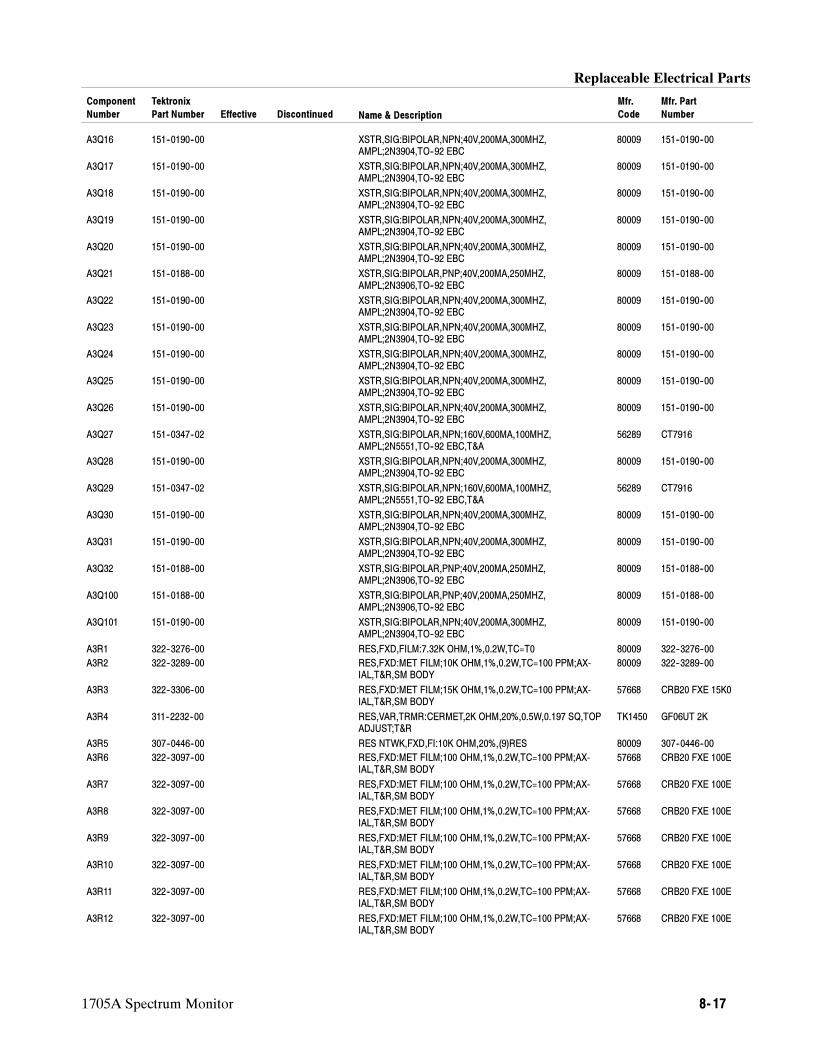
Replaceable Electrical Parts
1705A Spectrum Monitor 8- 17
Component
Number
Mfr. Part
Number
Mfr.
CodeName & DescriptionEffective Discontinued
Tektronix
Part Number
A3Q16 151--0190--00 XSTR,SIG:BIPOLAR,NPN;40V,200MA,300MHZ,AMPL;2N3904,TO--92 EBC
80009 151--0190--00
A3Q17 151--0190--00 XSTR,SIG:BIPOLAR,NPN;40V,200MA,300MHZ,AMPL;2N3904,TO--92 EBC
80009 151--0190--00
A3Q18 151--0190--00 XSTR,SIG:BIPOLAR,NPN;40V,200MA,300MHZ,AMPL;2N3904,TO--92 EBC
80009 151--0190--00
A3Q19 151--0190--00 XSTR,SIG:BIPOLAR,NPN;40V,200MA,300MHZ,AMPL;2N3904,TO--92 EBC
80009 151--0190--00
A3Q20 151--0190--00 XSTR,SIG:BIPOLAR,NPN;40V,200MA,300MHZ,AMPL;2N3904,TO--92 EBC
80009 151--0190--00
A3Q21 151--0188--00 XSTR,SIG:BIPOLAR,PNP;40V,200MA,250MHZ,AMPL;2N3906,TO--92 EBC
80009 151--0188--00
A3Q22 151--0190--00 XSTR,SIG:BIPOLAR,NPN;40V,200MA,300MHZ,AMPL;2N3904,TO--92 EBC
80009 151--0190--00
A3Q23 151--0190--00 XSTR,SIG:BIPOLAR,NPN;40V,200MA,300MHZ,AMPL;2N3904,TO--92 EBC
80009 151--0190--00
A3Q24 151--0190--00 XSTR,SIG:BIPOLAR,NPN;40V,200MA,300MHZ,AMPL;2N3904,TO--92 EBC
80009 151--0190--00
A3Q25 151--0190--00 XSTR,SIG:BIPOLAR,NPN;40V,200MA,300MHZ,AMPL;2N3904,TO--92 EBC
80009 151--0190--00
A3Q26 151--0190--00 XSTR,SIG:BIPOLAR,NPN;40V,200MA,300MHZ,AMPL;2N3904,TO--92 EBC
80009 151--0190--00
A3Q27 151--0347--02 XSTR,SIG:BIPOLAR,NPN;160V,600MA,100MHZ,AMPL;2N5551,TO--92 EBC,T&A
56289 CT7916
A3Q28 151--0190--00 XSTR,SIG:BIPOLAR,NPN;40V,200MA,300MHZ,AMPL;2N3904,TO--92 EBC
80009 151--0190--00
A3Q29 151--0347--02 XSTR,SIG:BIPOLAR,NPN;160V,600MA,100MHZ,AMPL;2N5551,TO--92 EBC,T&A
56289 CT7916
A3Q30 151--0190--00 XSTR,SIG:BIPOLAR,NPN;40V,200MA,300MHZ,AMPL;2N3904,TO--92 EBC
80009 151--0190--00
A3Q31 151--0190--00 XSTR,SIG:BIPOLAR,NPN;40V,200MA,300MHZ,AMPL;2N3904,TO--92 EBC
80009 151--0190--00
A3Q32 151--0188--00 XSTR,SIG:BIPOLAR,PNP;40V,200MA,250MHZ,AMPL;2N3906,TO--92 EBC
80009 151--0188--00
A3Q100 151--0188--00 XSTR,SIG:BIPOLAR,PNP;40V,200MA,250MHZ,AMPL;2N3906,TO--92 EBC
80009 151--0188--00
A3Q101 151--0190--00 XSTR,SIG:BIPOLAR,NPN;40V,200MA,300MHZ,AMPL;2N3904,TO--92 EBC
80009 151--0190--00
A3R1 322--3276--00 RES,FXD,FILM:7.32K OHM,1%,0.2W,TC=T0 80009 322--3276--00
A3R2 322--3289--00 RES,FXD:MET FILM;10K OHM,1%,0.2W,TC=100 PPM;AX-IAL,T&R,SM BODY
80009 322--3289--00
A3R3 322--3306--00 RES,FXD:MET FILM;15K OHM,1%,0.2W,TC=100 PPM;AX-IAL,T&R,SM BODY
57668 CRB20 FXE 15K0
A3R4 311--2232--00 RES,VAR,TRMR:CERMET,2K OHM,20%,0.5W,0.197 SQ,TOPADJUST;T&R
TK1450 GF06UT 2K
A3R5 307--0446--00 RES NTWK,FXD,FI:10K OHM,20%,(9)RES 80009 307--0446--00
A3R6 322--3097--00 RES,FXD:MET FILM;100 OHM,1%,0.2W,TC=100 PPM;AX-IAL,T&R,SM BODY
57668 CRB20 FXE 100E
A3R7 322--3097--00 RES,FXD:MET FILM;100 OHM,1%,0.2W,TC=100 PPM;AX-IAL,T&R,SM BODY
57668 CRB20 FXE 100E
A3R8 322--3097--00 RES,FXD:MET FILM;100 OHM,1%,0.2W,TC=100 PPM;AX-IAL,T&R,SM BODY
57668 CRB20 FXE 100E
A3R9 322--3097--00 RES,FXD:MET FILM;100 OHM,1%,0.2W,TC=100 PPM;AX-IAL,T&R,SM BODY
57668 CRB20 FXE 100E
A3R10 322--3097--00 RES,FXD:MET FILM;100 OHM,1%,0.2W,TC=100 PPM;AX-IAL,T&R,SM BODY
57668 CRB20 FXE 100E
A3R11 322--3097--00 RES,FXD:MET FILM;100 OHM,1%,0.2W,TC=100 PPM;AX-IAL,T&R,SM BODY
57668 CRB20 FXE 100E
A3R12 322--3097--00 RES,FXD:MET FILM;100 OHM,1%,0.2W,TC=100 PPM;AX-IAL,T&R,SM BODY
57668 CRB20 FXE 100E
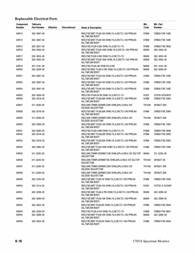
Replaceable Electrical Parts
8- 18 1705A Spectrum Monitor
Component
Number
Mfr. Part
Number
Mfr.
CodeName & DescriptionEffective Discontinued
Tektronix
Part Number
A3R13 322--3097--00 RES,FXD:MET FILM;100 OHM,1%,0.2W,TC=100 PPM;AX-IAL,T&R,SM BODY
57668 CRB20 FXE 100E
A3R14 322--3097--00 RES,FXD:MET FILM;100 OHM,1%,0.2W,TC=100 PPM;AX-IAL,T&R,SM BODY
57668 CRB20 FXE 100E
A3R15 322--3251--00 RES,FXD,FILM:4.02K OHM,1%,0.2W,TC=T0 57668 CRB20 FXE 4K02
A3R16 322--3402--00 RES,FXD:MET FILM;150K OHM,1%,0.2W,TC=100 PPM;AX-IAL,T&R,SM BODY
80009 322--3402--00
A3R17 322--3254--00 RES,FXD,FILM:4.32K OHM,1%,0.2W,TC=T0 80009 322--3254--00
A3R18 322--3402--00 RES,FXD:MET FILM;150K OHM,1%,0.2W,TC=100 PPM;AX-IAL,T&R,SM BODY
80009 322--3402--00
A3R19 301--0181--00 RES,FXD,FILM:180 OHM,5%,0.5W 80009 301--0181--00
A3R20 322--3258--00 RES,FXD:MET FILM;4.75K OHM,1%,0.2W,TC=100 PPM;AX-IAL,T&R,SM BODY
80009 322--3258--00
A3R21 322--3097--00 RES,FXD:MET FILM;100 OHM,1%,0.2W,TC=100 PPM;AX-IAL,T&R,SM BODY
57668 CRB20 FXE 100E
A3R23 322--3097--00 RES,FXD:MET FILM;100 OHM,1%,0.2W,TC=100 PPM;AX-IAL,T&R,SM BODY
57668 CRB20 FXE 100E
A3R24 322--3097--00 RES,FXD:MET FILM;100 OHM,1%,0.2W,TC=100 PPM;AX-IAL,T&R,SM BODY
57668 CRB20 FXE 100E
A3R25 322--3326--00 RES,FXD,FILM:24.3K OHM,1%,0.2W,TC--T0 91637 CCF50--2F24301F
A3R26 322--3318--00 RES,FXD:MET FILM;20K OHM,1%,0.2W,TC=100 PPM;AX-IAL,T&R,SM BODY
57668 CRB20 FXE 20K0
A3R27 311--2236--00 RES,VAR,TRMR:CERMET;20K OHM,20%,0.5W,0.197SQ,SIDE ADJUST;T&R
TK1450 GF06UT 20K
A3R28 322--3318--00 RES,FXD:MET FILM;20K OHM,1%,0.2W,TC=100 PPM;AX-IAL,T&R,SM BODY
57668 CRB20 FXE 20K0
A3R29 311--2236--00 RES,VAR,TRMR:CERMET;20K OHM,20%,0.5W,0.197SQ,SIDE ADJUST;T&R
TK1450 GF06UT 20K
A3R30 322--3306--00 RES,FXD:MET FILM;15K OHM,1%,0.2W,TC=100 PPM;AX-IAL,T&R,SM BODY
57668 CRB20 FXE 15K0
A3R31 322--3260--00 RES,FXD,FILM:4.99K OHM,1%,0.2W,TC=T0 57668 CRB20 FXE 4K99
A3R32 322--3318--00 RES,FXD:MET FILM;20K OHM,1%,0.2W,TC=100 PPM;AX-IAL,T&R,SM BODY
57668 CRB20 FXE 20K0
A3R33 322--3318--00 RES,FXD:MET FILM;20K OHM,1%,0.2W,TC=100 PPM;AX-IAL,T&R,SM BODY
57668 CRB20 FXE 20K0
A3R34 322--3385--00 RES,FXD:MET FILM;100K OHM,1%,0.2W,TC=100 PPM;AX-IAL,T&R,SM BODY
57668 CRB20 FXE 100K
A3R35 311--2235--00 RES,VAR,TRMR:CERMET;10K OHM,20%,0.5W,0.197 SQ,TOPADJUST;T&R
80009 311--2235--00
A3R36 311--2234--00 RES,VAR,TRMR:CERMET;5K OHM,20%,0.5W,0.197 SQ,TOPADJUST;T&R
TK1450 GF06UT 5K
A3R37 311--2236--00 RES,VAR,TRMR:CERMET;20K OHM,20%,0.5W,0.197SQ,SIDE ADJUST;T&R
TK1450 GF06UT 20K
A3R38 311--2236--00 RES,VAR,TRMR:CERMET;20K OHM,20%,0.5W,0.197SQ,SIDE ADJUST;T&R
TK1450 GF06UT 20K
A3R39 322--3193--00 RES,FXD:MET FILM;1K OHM,1%,0.2W,TC=100 PPM;AX-IAL,T&R,SM BODY
57668 CRB20 FXE 1K00
A3R40 322--3114--00 RES,FXD:MET FILM;150 OHM,1%,0.2W,TC=100 PPM;AX-IAL,T&R,SM BODY
91637 CCF50--2--G1500F
A3R41 322--3258--00 RES,FXD:MET FILM;4.75K OHM,1%,0.2W,TC=100 PPM;AX-IAL,T&R,SM BODY
80009 322--3258--00
A3R42 322--3289--00 RES,FXD:MET FILM;10K OHM,1%,0.2W,TC=100 PPM;AX-IAL,T&R,SM BODY
80009 322--3289--00
A3R43 322--3222--00 RES,FXD:MET FILM;2K OHM,1%,0.2W,TC=100 PPM;AX-IAL,T&R,SM BODY
57668 CRB20 FXE 2K00
A3R44 322--3239--00 RES,FXD,FILM:3.01K OHM,1%,0.2W,TC=T0 57668 CRB20 FXE 3K01
A3R45 322--3289--00 RES,FXD:MET FILM;10K OHM,1%,0.2W,TC=100 PPM;AX-IAL,T&R,SM BODY
80009 322--3289--00
A3R46 322--3222--00 RES,FXD:MET FILM;2K OHM,1%,0.2W,TC=100 PPM;AX-IAL,T&R,SM BODY
57668 CRB20 FXE 2K00
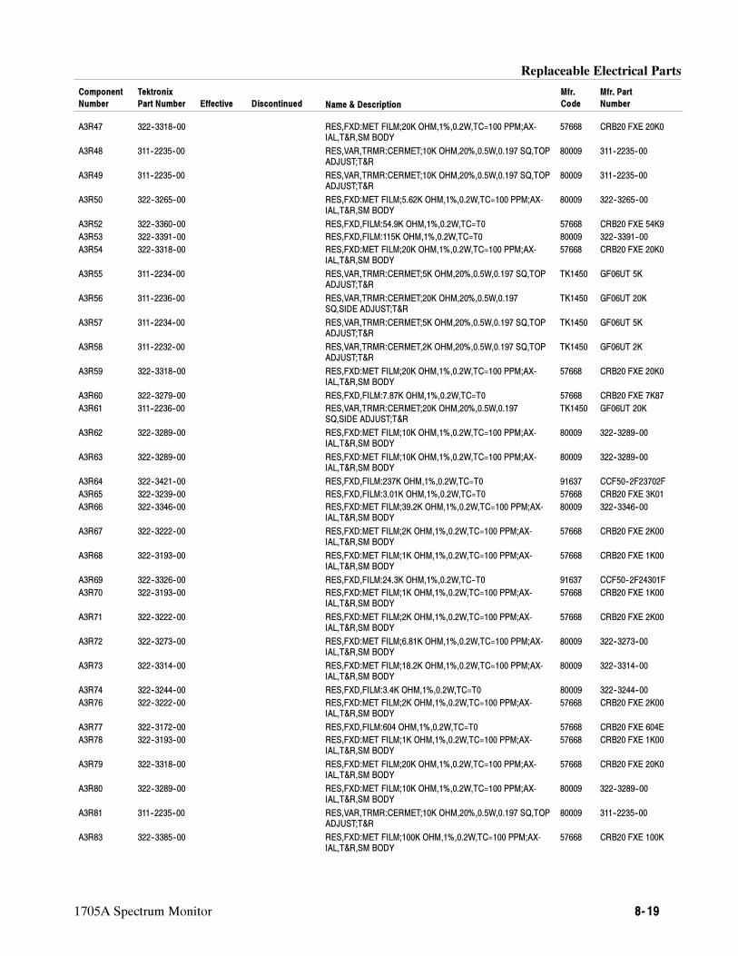
Replaceable Electrical Parts
1705A Spectrum Monitor 8- 19
Component
Number
Mfr. Part
Number
Mfr.
CodeName & DescriptionEffective Discontinued
Tektronix
Part Number
A3R47 322--3318--00 RES,FXD:MET FILM;20K OHM,1%,0.2W,TC=100 PPM;AX-IAL,T&R,SM BODY
57668 CRB20 FXE 20K0
A3R48 311--2235--00 RES,VAR,TRMR:CERMET;10K OHM,20%,0.5W,0.197 SQ,TOPADJUST;T&R
80009 311--2235--00
A3R49 311--2235--00 RES,VAR,TRMR:CERMET;10K OHM,20%,0.5W,0.197 SQ,TOPADJUST;T&R
80009 311--2235--00
A3R50 322--3265--00 RES,FXD:MET FILM;5.62K OHM,1%,0.2W,TC=100 PPM;AX-IAL,T&R,SM BODY
80009 322--3265--00
A3R52 322--3360--00 RES,FXD,FILM:54.9K OHM,1%,0.2W,TC=T0 57668 CRB20 FXE 54K9
A3R53 322--3391--00 RES,FXD,FILM:115K OHM,1%,0.2W,TC=T0 80009 322--3391--00
A3R54 322--3318--00 RES,FXD:MET FILM;20K OHM,1%,0.2W,TC=100 PPM;AX-IAL,T&R,SM BODY
57668 CRB20 FXE 20K0
A3R55 311--2234--00 RES,VAR,TRMR:CERMET;5K OHM,20%,0.5W,0.197 SQ,TOPADJUST;T&R
TK1450 GF06UT 5K
A3R56 311--2236--00 RES,VAR,TRMR:CERMET;20K OHM,20%,0.5W,0.197SQ,SIDE ADJUST;T&R
TK1450 GF06UT 20K
A3R57 311--2234--00 RES,VAR,TRMR:CERMET;5K OHM,20%,0.5W,0.197 SQ,TOPADJUST;T&R
TK1450 GF06UT 5K
A3R58 311--2232--00 RES,VAR,TRMR:CERMET,2K OHM,20%,0.5W,0.197 SQ,TOPADJUST;T&R
TK1450 GF06UT 2K
A3R59 322--3318--00 RES,FXD:MET FILM;20K OHM,1%,0.2W,TC=100 PPM;AX-IAL,T&R,SM BODY
57668 CRB20 FXE 20K0
A3R60 322--3279--00 RES,FXD,FILM:7.87K OHM,1%,0.2W,TC=T0 57668 CRB20 FXE 7K87
A3R61 311--2236--00 RES,VAR,TRMR:CERMET;20K OHM,20%,0.5W,0.197SQ,SIDE ADJUST;T&R
TK1450 GF06UT 20K
A3R62 322--3289--00 RES,FXD:MET FILM;10K OHM,1%,0.2W,TC=100 PPM;AX-IAL,T&R,SM BODY
80009 322--3289--00
A3R63 322--3289--00 RES,FXD:MET FILM;10K OHM,1%,0.2W,TC=100 PPM;AX-IAL,T&R,SM BODY
80009 322--3289--00
A3R64 322--3421--00 RES,FXD,FILM:237K OHM,1%,0.2W,TC=T0 91637 CCF50--2F23702F
A3R65 322--3239--00 RES,FXD,FILM:3.01K OHM,1%,0.2W,TC=T0 57668 CRB20 FXE 3K01
A3R66 322--3346--00 RES,FXD:MET FILM;39.2K OHM,1%,0.2W,TC=100 PPM;AX-IAL,T&R,SM BODY
80009 322--3346--00
A3R67 322--3222--00 RES,FXD:MET FILM;2K OHM,1%,0.2W,TC=100 PPM;AX-IAL,T&R,SM BODY
57668 CRB20 FXE 2K00
A3R68 322--3193--00 RES,FXD:MET FILM;1K OHM,1%,0.2W,TC=100 PPM;AX-IAL,T&R,SM BODY
57668 CRB20 FXE 1K00
A3R69 322--3326--00 RES,FXD,FILM:24.3K OHM,1%,0.2W,TC--T0 91637 CCF50--2F24301F
A3R70 322--3193--00 RES,FXD:MET FILM;1K OHM,1%,0.2W,TC=100 PPM;AX-IAL,T&R,SM BODY
57668 CRB20 FXE 1K00
A3R71 322--3222--00 RES,FXD:MET FILM;2K OHM,1%,0.2W,TC=100 PPM;AX-IAL,T&R,SM BODY
57668 CRB20 FXE 2K00
A3R72 322--3273--00 RES,FXD:MET FILM;6.81K OHM,1%,0.2W,TC=100 PPM;AX-IAL,T&R,SM BODY
80009 322--3273--00
A3R73 322--3314--00 RES,FXD:MET FILM;18.2K OHM,1%,0.2W,TC=100 PPM;AX-IAL,T&R,SM BODY
80009 322--3314--00
A3R74 322--3244--00 RES,FXD,FILM:3.4K OHM,1%,0.2W,TC=T0 80009 322--3244--00
A3R76 322--3222--00 RES,FXD:MET FILM;2K OHM,1%,0.2W,TC=100 PPM;AX-IAL,T&R,SM BODY
57668 CRB20 FXE 2K00
A3R77 322--3172--00 RES,FXD,FILM:604 OHM,1%,0.2W,TC=T0 57668 CRB20 FXE 604E
A3R78 322--3193--00 RES,FXD:MET FILM;1K OHM,1%,0.2W,TC=100 PPM;AX-IAL,T&R,SM BODY
57668 CRB20 FXE 1K00
A3R79 322--3318--00 RES,FXD:MET FILM;20K OHM,1%,0.2W,TC=100 PPM;AX-IAL,T&R,SM BODY
57668 CRB20 FXE 20K0
A3R80 322--3289--00 RES,FXD:MET FILM;10K OHM,1%,0.2W,TC=100 PPM;AX-IAL,T&R,SM BODY
80009 322--3289--00
A3R81 311--2235--00 RES,VAR,TRMR:CERMET;10K OHM,20%,0.5W,0.197 SQ,TOPADJUST;T&R
80009 311--2235--00
A3R83 322--3385--00 RES,FXD:MET FILM;100K OHM,1%,0.2W,TC=100 PPM;AX-IAL,T&R,SM BODY
57668 CRB20 FXE 100K
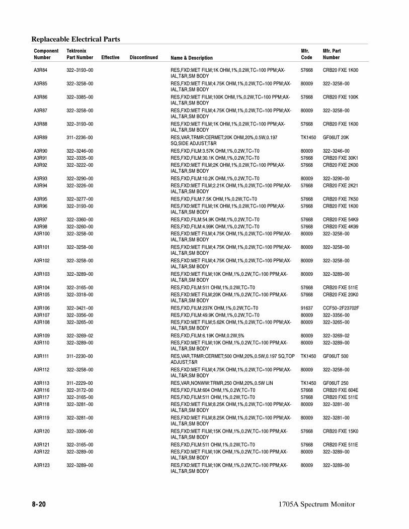
Replaceable Electrical Parts
8- 20 1705A Spectrum Monitor
Component
Number
Mfr. Part
Number
Mfr.
CodeName & DescriptionEffective Discontinued
Tektronix
Part Number
A3R84 322--3193--00 RES,FXD:MET FILM;1K OHM,1%,0.2W,TC=100 PPM;AX-IAL,T&R,SM BODY
57668 CRB20 FXE 1K00
A3R85 322--3258--00 RES,FXD:MET FILM;4.75K OHM,1%,0.2W,TC=100 PPM;AX-IAL,T&R,SM BODY
80009 322--3258--00
A3R86 322--3385--00 RES,FXD:MET FILM;100K OHM,1%,0.2W,TC=100 PPM;AX-IAL,T&R,SM BODY
57668 CRB20 FXE 100K
A3R87 322--3258--00 RES,FXD:MET FILM;4.75K OHM,1%,0.2W,TC=100 PPM;AX-IAL,T&R,SM BODY
80009 322--3258--00
A3R88 322--3193--00 RES,FXD:MET FILM;1K OHM,1%,0.2W,TC=100 PPM;AX-IAL,T&R,SM BODY
57668 CRB20 FXE 1K00
A3R89 311--2236--00 RES,VAR,TRMR:CERMET;20K OHM,20%,0.5W,0.197SQ,SIDE ADJUST;T&R
TK1450 GF06UT 20K
A3R90 322--3246--00 RES,FXD,FILM:3.57K OHM,1%,0.2W,TC=T0 80009 322--3246--00
A3R91 322--3335--00 RES,FXD,FILM:30.1K OHM,1%,0.2W,TC=T0 57668 CRB20 FXE 30K1
A3R92 322--3222--00 RES,FXD:MET FILM;2K OHM,1%,0.2W,TC=100 PPM;AX-IAL,T&R,SM BODY
57668 CRB20 FXE 2K00
A3R93 322--3290--00 RES,FXD,FILM:10.2K OHM,1%,0.2W,TC=T0 80009 322--3290--00
A3R94 322--3226--00 RES,FXD:MET FILM;2.21K OHM,1%,0.2W,TC=100 PPM;AX-IAL,T&R,SM BODY
57668 CRB20 FXE 2K21
A3R95 322--3277--00 RES,FXD,FILM:7.5K OHM,1%,0.2W,TC=T0 57668 CRB20 FXE 7K50
A3R96 322--3193--00 RES,FXD:MET FILM;1K OHM,1%,0.2W,TC=100 PPM;AX-IAL,T&R,SM BODY
57668 CRB20 FXE 1K00
A3R97 322--3360--00 RES,FXD,FILM:54.9K OHM,1%,0.2W,TC=T0 57668 CRB20 FXE 54K9
A3R98 322--3260--00 RES,FXD,FILM:4.99K OHM,1%,0.2W,TC=T0 57668 CRB20 FXE 4K99
A3R100 322--3258--00 RES,FXD:MET FILM;4.75K OHM,1%,0.2W,TC=100 PPM;AX-IAL,T&R,SM BODY
80009 322--3258--00
A3R101 322--3258--00 RES,FXD:MET FILM;4.75K OHM,1%,0.2W,TC=100 PPM;AX-IAL,T&R,SM BODY
80009 322--3258--00
A3R102 322--3258--00 RES,FXD:MET FILM;4.75K OHM,1%,0.2W,TC=100 PPM;AX-IAL,T&R,SM BODY
80009 322--3258--00
A3R103 322--3289--00 RES,FXD:MET FILM;10K OHM,1%,0.2W,TC=100 PPM;AX-IAL,T&R,SM BODY
80009 322--3289--00
A3R104 322--3165--00 RES,FXD,FILM:511 OHM,1%,0.2W,TC=T0 57668 CRB20 FXE 511E
A3R105 322--3318--00 RES,FXD:MET FILM;20K OHM,1%,0.2W,TC=100 PPM;AX-IAL,T&R,SM BODY
57668 CRB20 FXE 20K0
A3R106 322--3421--00 RES,FXD,FILM:237K OHM,1%,0.2W,TC=T0 91637 CCF50--2F23702F
A3R107 322--3356--00 RES,FXD,FILM:49.9K OHM,1%,0.2W,TC=T0 80009 322--3356--00
A3R108 322--3265--00 RES,FXD:MET FILM;5.62K OHM,1%,0.2W,TC=100 PPM;AX-IAL,T&R,SM BODY
80009 322--3265--00
A3R109 322--3269--02 RES,FXD,FILM:6.19K OHM,0.2W,5% 80009 322--3269--02
A3R110 322--3289--00 RES,FXD:MET FILM;10K OHM,1%,0.2W,TC=100 PPM;AX-IAL,T&R,SM BODY
80009 322--3289--00
A3R111 311--2230--00 RES,VAR,TRMR:CERMET;500 OHM,20%,0.5W,0.197 SQ,TOPADJUST;T&R
TK1450 GF06UT 500
A3R112 322--3258--00 RES,FXD:MET FILM;4.75K OHM,1%,0.2W,TC=100 PPM;AX-IAL,T&R,SM BODY
80009 322--3258--00
A3R113 311--2229--00 RES,VAR,NONWW:TRMR,250 OHM,20%,0.5W LIN TK1450 GF06UT 250
A3R116 322--3172--00 RES,FXD,FILM:604 OHM,1%,0.2W,TC=T0 57668 CRB20 FXE 604E
A3R117 322--3165--00 RES,FXD,FILM:511 OHM,1%,0.2W,TC=T0 57668 CRB20 FXE 511E
A3R118 322--3281--00 RES,FXD:MET FILM;8.25K OHM,1%,0.2W,TC=100 PPM;AX-IAL,T&R,SM BODY
80009 322--3281--00
A3R119 322--3281--00 RES,FXD:MET FILM;8.25K OHM,1%,0.2W,TC=100 PPM;AX-IAL,T&R,SM BODY
80009 322--3281--00
A3R120 322--3306--00 RES,FXD:MET FILM;15K OHM,1%,0.2W,TC=100 PPM;AX-IAL,T&R,SM BODY
57668 CRB20 FXE 15K0
A3R121 322--3165--00 RES,FXD,FILM:511 OHM,1%,0.2W,TC=T0 57668 CRB20 FXE 511E
A3R122 322--3289--00 RES,FXD:MET FILM;10K OHM,1%,0.2W,TC=100 PPM;AX-IAL,T&R,SM BODY
80009 322--3289--00
A3R123 322--3289--00 RES,FXD:MET FILM;10K OHM,1%,0.2W,TC=100 PPM;AX-IAL,T&R,SM BODY
80009 322--3289--00
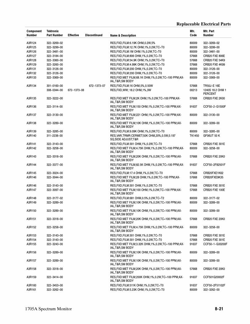
Replaceable Electrical Parts
1705A Spectrum Monitor 8- 21
Component
Number
Mfr. Part
Number
Mfr.
CodeName & DescriptionEffective Discontinued
Tektronix
Part Number
A3R124 322--3269--02 RES,FXD,FILM:6.19K OHM,0.2W,5% 80009 322--3269--02
A3R125 322--3299--00 RES,FXD,FILM:12.7K OHM,1%,0.2W,TC=T0 80009 322--3299--00
A3R126 322--3481--00 RES,FXD,FILM:1M OHM.1%,0.2W,TC=T0 80009 322--3481--00
A3R127 322--3184--00 RES,FXD,FILM:806 OHM,1%,0.2W,TC=T0 57668 CRB20 FXE 806E
A3R128 322--3360--00 RES,FXD,FILM:54.9K OHM,1%,0.2W,TC=T0 57668 CRB20 FXE 54K9
A3R129 322--3260--00 RES,FXD,FILM:4.99K OHM,1%,0.2W,TC=T0 57668 CRB20 FXE 4K99
A3R131 322--3126--00 RES,FXD,FILM:200 OHM,1%,0.2W,TC=T0 80009 322--3126--00
A3R132 322--3126--00 RES,FXD,FILM:200 OHM,1%,0.2W,TC=T0 80009 322--3126--00
A3R133 322--3369--00 RES,FXD:MET FILM;68.1K OHM,1%,0.2W,TC=100 PPM;AX-IAL,T&R,SM BODY
80009 322--3369--00
A3R134 301--0160--00 672--1373--07 RES,FXD,FILM:16 OHM,5%,0.50W 57668 TR50J--E 16E
308--0344--00 672--1373--08 RES,FXD,WW; 18.2 OHM,1%,3W 00213 1240S 18.2 OHM 1PERCENT
A3R135 322--3222--00 RES,FXD:MET FILM;2K OHM,1%,0.2W,TC=100 PPM;AX-IAL,T&R,SM BODY
57668 CRB20 FXE 2K00
A3R136 322--3114--00 RES,FXD:MET FILM;150 OHM,1%,0.2W,TC=100 PPM;AX-IAL,T&R,SM BODY
91637 CCF50--2--G1500F
A3R137 322--3130--00 RES,FXD:MET FILM;221 OHM,1%,0.2W,TC=100 PPM;AX-IAL,T&R,SM BODY
80009 322--3130--00
A3R138 322--3289--00 RES,FXD:MET FILM;10K OHM,1%,0.2W,TC=100 PPM;AX-IAL,T&R,SM BODY
80009 322--3289--00
A3R139 322--3285--00 RES,FXD,FILM:9.09K OHM,1%,0.2W,TC=T0 80009 322--3285--00
A3R140 311--2238--00 RES,VAR,TRMR:CERMET;50K OHM,20%,0.5W,0.197SQ,SIDE ADJUST;T&R
TK1450 GF06UT 50 K
A3R141 322--3143--00 RES,FXD,FILM:301 OHM,1%,0.2W,TC=T0 57668 CRB20 FXE 301E
A3R142 322--3258--00 RES,FXD:MET FILM;4.75K OHM,1%,0.2W,TC=100 PPM;AX-IAL,T&R,SM BODY
80009 322--3258--00
A3R143 322--3318--00 RES,FXD:MET FILM;20K OHM,1%,0.2W,TC=100 PPM;AX-IAL,T&R,SM BODY
57668 CRB20 FXE 20K0
A3R144 322--3377--00 RES,FXD:MET FILM;82.5K OHM,1%,0.2W,TC=100 PPM;AX-IAL,T&R,SM BODY
91637 CCF50--2F82501F
A3R145 322--3024--00 RES,FXD,FILM:17.4 OHM,1%,0.2W,TC=T0 57668 CRB20FXE1K62
A3R146 322--3044--00 RES,FXD:MET FILM;28 OHM,1%,0.2W,TC=100 PPM;AX-IAL,T&R,SM BODY
57668 CRB20FXE9K35
A3R146 322--3143--00 RES,FXD,FILM:301 OHM,1%,0.2W,TC=T0 57668 CRB20 FXE 301E
A3R147 322--3097--00 RES,FXD:MET FILM;100 OHM,1%,0.2W,TC=100 PPM;AX-IAL,T&R,SM BODY
57668 CRB20 FXE 100E
A3R148 322--3177--02 RES,FXD,FILM:681 OHM,0.5%,0.2W,TC=T2 80009 322--3177--02
A3R149 322--3289--00 RES,FXD:MET FILM;10K OHM,1%,0.2W,TC=100 PPM;AX-IAL,T&R,SM BODY
80009 322--3289--00
A3R150 322--3289--00 RES,FXD:MET FILM;10K OHM,1%,0.2W,TC=100 PPM;AX-IAL,T&R,SM BODY
80009 322--3289--00
A3R151 322--3318--00 RES,FXD:MET FILM;20K OHM,1%,0.2W,TC=100 PPM;AX-IAL,T&R,SM BODY
57668 CRB20 FXE 20K0
A3R152 322--3258--00 RES,FXD:MET FILM;4.75K OHM,1%,0.2W,TC=100 PPM;AX-IAL,T&R,SM BODY
80009 322--3258--00
A3R153 322--3143--00 RES,FXD,FILM:301 OHM,1%,0.2W,TC=T0 57668 CRB20 FXE 301E
A3R154 322--3143--00 RES,FXD,FILM:301 OHM,1%,0.2W,TC=T0 57668 CRB20 FXE 301E
A3R155 322--3243--00 RES,FXD:MET FILM;3.32K OHM,1%,0.2W,TC=100 PPM;AX-IAL,T&R,SM BODY
91637 CCF50--1--G33200F
A3R156 322--3289--00 RES,FXD:MET FILM;10K OHM,1%,0.2W,TC=100 PPM;AX-IAL,T&R,SM BODY
80009 322--3289--00
A3R157 322--3289--00 RES,FXD:MET FILM;10K OHM,1%,0.2W,TC=100 PPM;AX-IAL,T&R,SM BODY
80009 322--3289--00
A3R158 322--3318--00 RES,FXD:MET FILM;20K OHM,1%,0.2W,TC=100 PPM;AX-IAL,T&R,SM BODY
57668 CRB20 FXE 20K0
A3R159 322--3414--00 RES,FXD:MET FILM;200K OHM,1%,0.2W,TC=100 PPM;AX-IAL,T&R,SM BODY
91637 CCF501G20002F
A3R160 322--3453--00 RES,FXD,FILM:511K OHM,1%,0.2W,TC=T0 91637 CCF50--2F51102F
A3R161 322--3262--00 RES,FXD,FILM:5.23K OHM,1%,0.2W,TC=T0 80009 322--3262--00
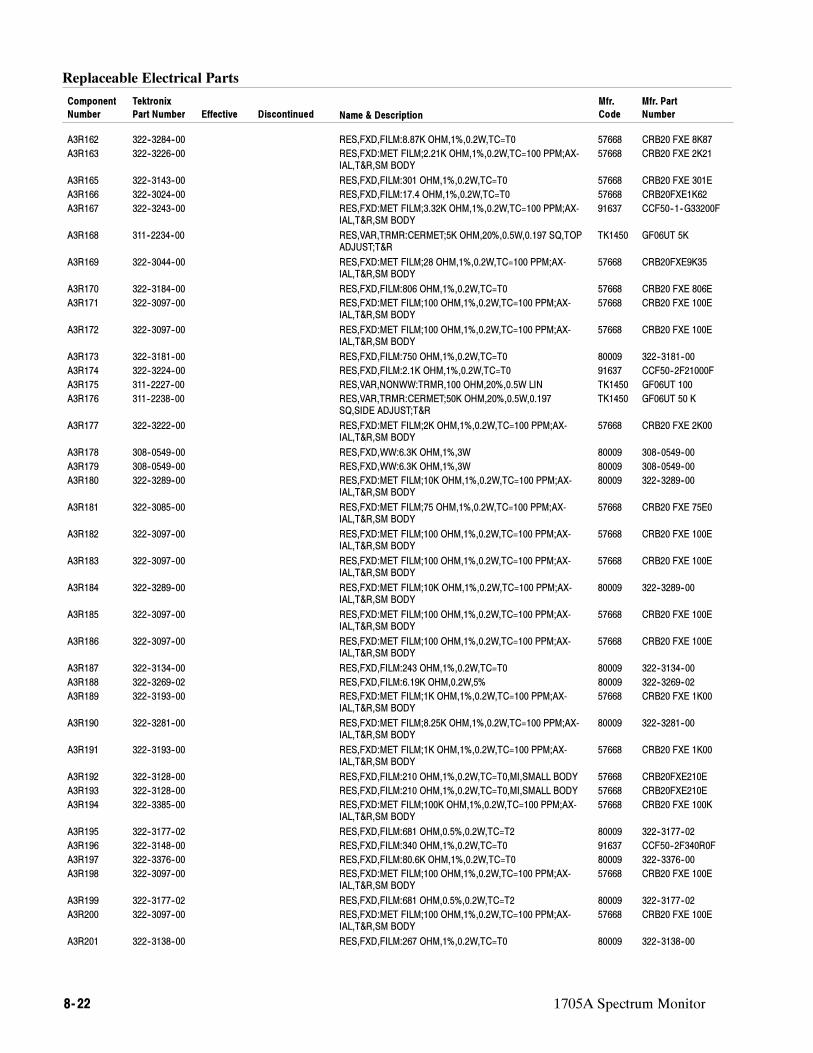
Replaceable Electrical Parts
8- 22 1705A Spectrum Monitor
Component
Number
Mfr. Part
Number
Mfr.
CodeName & DescriptionEffective Discontinued
Tektronix
Part Number
A3R162 322--3284--00 RES,FXD,FILM:8.87K OHM,1%,0.2W,TC=T0 57668 CRB20 FXE 8K87
A3R163 322--3226--00 RES,FXD:MET FILM;2.21K OHM,1%,0.2W,TC=100 PPM;AX-IAL,T&R,SM BODY
57668 CRB20 FXE 2K21
A3R165 322--3143--00 RES,FXD,FILM:301 OHM,1%,0.2W,TC=T0 57668 CRB20 FXE 301E
A3R166 322--3024--00 RES,FXD,FILM:17.4 OHM,1%,0.2W,TC=T0 57668 CRB20FXE1K62
A3R167 322--3243--00 RES,FXD:MET FILM;3.32K OHM,1%,0.2W,TC=100 PPM;AX-IAL,T&R,SM BODY
91637 CCF50--1--G33200F
A3R168 311--2234--00 RES,VAR,TRMR:CERMET;5K OHM,20%,0.5W,0.197 SQ,TOPADJUST;T&R
TK1450 GF06UT 5K
A3R169 322--3044--00 RES,FXD:MET FILM;28 OHM,1%,0.2W,TC=100 PPM;AX-IAL,T&R,SM BODY
57668 CRB20FXE9K35
A3R170 322--3184--00 RES,FXD,FILM:806 OHM,1%,0.2W,TC=T0 57668 CRB20 FXE 806E
A3R171 322--3097--00 RES,FXD:MET FILM;100 OHM,1%,0.2W,TC=100 PPM;AX-IAL,T&R,SM BODY
57668 CRB20 FXE 100E
A3R172 322--3097--00 RES,FXD:MET FILM;100 OHM,1%,0.2W,TC=100 PPM;AX-IAL,T&R,SM BODY
57668 CRB20 FXE 100E
A3R173 322--3181--00 RES,FXD,FILM:750 OHM,1%,0.2W,TC=T0 80009 322--3181--00
A3R174 322--3224--00 RES,FXD,FILM:2.1K OHM,1%,0.2W,TC=T0 91637 CCF50--2F21000F
A3R175 311--2227--00 RES,VAR,NONWW:TRMR,100 OHM,20%,0.5W LIN TK1450 GF06UT 100
A3R176 311--2238--00 RES,VAR,TRMR:CERMET;50K OHM,20%,0.5W,0.197SQ,SIDE ADJUST;T&R
TK1450 GF06UT 50 K
A3R177 322--3222--00 RES,FXD:MET FILM;2K OHM,1%,0.2W,TC=100 PPM;AX-IAL,T&R,SM BODY
57668 CRB20 FXE 2K00
A3R178 308--0549--00 RES,FXD,WW:6.3K OHM,1%,3W 80009 308--0549--00
A3R179 308--0549--00 RES,FXD,WW:6.3K OHM,1%,3W 80009 308--0549--00
A3R180 322--3289--00 RES,FXD:MET FILM;10K OHM,1%,0.2W,TC=100 PPM;AX-IAL,T&R,SM BODY
80009 322--3289--00
A3R181 322--3085--00 RES,FXD:MET FILM;75 OHM,1%,0.2W,TC=100 PPM;AX-IAL,T&R,SM BODY
57668 CRB20 FXE 75E0
A3R182 322--3097--00 RES,FXD:MET FILM;100 OHM,1%,0.2W,TC=100 PPM;AX-IAL,T&R,SM BODY
57668 CRB20 FXE 100E
A3R183 322--3097--00 RES,FXD:MET FILM;100 OHM,1%,0.2W,TC=100 PPM;AX-IAL,T&R,SM BODY
57668 CRB20 FXE 100E
A3R184 322--3289--00 RES,FXD:MET FILM;10K OHM,1%,0.2W,TC=100 PPM;AX-IAL,T&R,SM BODY
80009 322--3289--00
A3R185 322--3097--00 RES,FXD:MET FILM;100 OHM,1%,0.2W,TC=100 PPM;AX-IAL,T&R,SM BODY
57668 CRB20 FXE 100E
A3R186 322--3097--00 RES,FXD:MET FILM;100 OHM,1%,0.2W,TC=100 PPM;AX-IAL,T&R,SM BODY
57668 CRB20 FXE 100E
A3R187 322--3134--00 RES,FXD,FILM:243 OHM,1%,0.2W,TC=T0 80009 322--3134--00
A3R188 322--3269--02 RES,FXD,FILM:6.19K OHM,0.2W,5% 80009 322--3269--02
A3R189 322--3193--00 RES,FXD:MET FILM;1K OHM,1%,0.2W,TC=100 PPM;AX-IAL,T&R,SM BODY
57668 CRB20 FXE 1K00
A3R190 322--3281--00 RES,FXD:MET FILM;8.25K OHM,1%,0.2W,TC=100 PPM;AX-IAL,T&R,SM BODY
80009 322--3281--00
A3R191 322--3193--00 RES,FXD:MET FILM;1K OHM,1%,0.2W,TC=100 PPM;AX-IAL,T&R,SM BODY
57668 CRB20 FXE 1K00
A3R192 322--3128--00 RES,FXD,FILM:210 OHM,1%,0.2W,TC=T0,MI,SMALL BODY 57668 CRB20FXE210E
A3R193 322--3128--00 RES,FXD,FILM:210 OHM,1%,0.2W,TC=T0,MI,SMALL BODY 57668 CRB20FXE210E
A3R194 322--3385--00 RES,FXD:MET FILM;100K OHM,1%,0.2W,TC=100 PPM;AX-IAL,T&R,SM BODY
57668 CRB20 FXE 100K
A3R195 322--3177--02 RES,FXD,FILM:681 OHM,0.5%,0.2W,TC=T2 80009 322--3177--02
A3R196 322--3148--00 RES,FXD,FILM:340 OHM,1%,0.2W,TC=T0 91637 CCF50--2F340R0F
A3R197 322--3376--00 RES,FXD,FILM:80.6K OHM,1%,0.2W,TC=T0 80009 322--3376--00
A3R198 322--3097--00 RES,FXD:MET FILM;100 OHM,1%,0.2W,TC=100 PPM;AX-IAL,T&R,SM BODY
57668 CRB20 FXE 100E
A3R199 322--3177--02 RES,FXD,FILM:681 OHM,0.5%,0.2W,TC=T2 80009 322--3177--02
A3R200 322--3097--00 RES,FXD:MET FILM;100 OHM,1%,0.2W,TC=100 PPM;AX-IAL,T&R,SM BODY
57668 CRB20 FXE 100E
A3R201 322--3138--00 RES,FXD,FILM:267 OHM,1%,0.2W,TC=T0 80009 322--3138--00
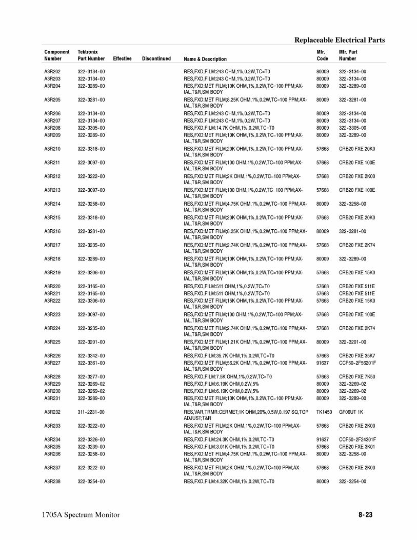
Replaceable Electrical Parts
1705A Spectrum Monitor 8- 23
Component
Number
Mfr. Part
Number
Mfr.
CodeName & DescriptionEffective Discontinued
Tektronix
Part Number
A3R202 322--3134--00 RES,FXD,FILM:243 OHM,1%,0.2W,TC=T0 80009 322--3134--00
A3R203 322--3134--00 RES,FXD,FILM:243 OHM,1%,0.2W,TC=T0 80009 322--3134--00
A3R204 322--3289--00 RES,FXD:MET FILM;10K OHM,1%,0.2W,TC=100 PPM;AX-IAL,T&R,SM BODY
80009 322--3289--00
A3R205 322--3281--00 RES,FXD:MET FILM;8.25K OHM,1%,0.2W,TC=100 PPM;AX-IAL,T&R,SM BODY
80009 322--3281--00
A3R206 322--3134--00 RES,FXD,FILM:243 OHM,1%,0.2W,TC=T0 80009 322--3134--00
A3R207 322--3134--00 RES,FXD,FILM:243 OHM,1%,0.2W,TC=T0 80009 322--3134--00
A3R208 322--3305--00 RES,FXD,FILM:14.7K OHM,1%,0.2W,TC=T0 80009 322--3305--00
A3R209 322--3289--00 RES,FXD:MET FILM;10K OHM,1%,0.2W,TC=100 PPM;AX-IAL,T&R,SM BODY
80009 322--3289--00
A3R210 322--3318--00 RES,FXD:MET FILM;20K OHM,1%,0.2W,TC=100 PPM;AX-IAL,T&R,SM BODY
57668 CRB20 FXE 20K0
A3R211 322--3097--00 RES,FXD:MET FILM;100 OHM,1%,0.2W,TC=100 PPM;AX-IAL,T&R,SM BODY
57668 CRB20 FXE 100E
A3R212 322--3222--00 RES,FXD:MET FILM;2K OHM,1%,0.2W,TC=100 PPM;AX-IAL,T&R,SM BODY
57668 CRB20 FXE 2K00
A3R213 322--3097--00 RES,FXD:MET FILM;100 OHM,1%,0.2W,TC=100 PPM;AX-IAL,T&R,SM BODY
57668 CRB20 FXE 100E
A3R214 322--3258--00 RES,FXD:MET FILM;4.75K OHM,1%,0.2W,TC=100 PPM;AX-IAL,T&R,SM BODY
80009 322--3258--00
A3R215 322--3318--00 RES,FXD:MET FILM;20K OHM,1%,0.2W,TC=100 PPM;AX-IAL,T&R,SM BODY
57668 CRB20 FXE 20K0
A3R216 322--3281--00 RES,FXD:MET FILM;8.25K OHM,1%,0.2W,TC=100 PPM;AX-IAL,T&R,SM BODY
80009 322--3281--00
A3R217 322--3235--00 RES,FXD:MET FILM;2.74K OHM,1%,0.2W,TC=100 PPM;AX-IAL,T&R,SM BODY
57668 CRB20 FXE 2K74
A3R218 322--3289--00 RES,FXD:MET FILM;10K OHM,1%,0.2W,TC=100 PPM;AX-IAL,T&R,SM BODY
80009 322--3289--00
A3R219 322--3306--00 RES,FXD:MET FILM;15K OHM,1%,0.2W,TC=100 PPM;AX-IAL,T&R,SM BODY
57668 CRB20 FXE 15K0
A3R220 322--3165--00 RES,FXD,FILM:511 OHM,1%,0.2W,TC=T0 57668 CRB20 FXE 511E
A3R221 322--3165--00 RES,FXD,FILM:511 OHM,1%,0.2W,TC=T0 57668 CRB20 FXE 511E
A3R222 322--3306--00 RES,FXD:MET FILM;15K OHM,1%,0.2W,TC=100 PPM;AX-IAL,T&R,SM BODY
57668 CRB20 FXE 15K0
A3R223 322--3097--00 RES,FXD:MET FILM;100 OHM,1%,0.2W,TC=100 PPM;AX-IAL,T&R,SM BODY
57668 CRB20 FXE 100E
A3R224 322--3235--00 RES,FXD:MET FILM;2.74K OHM,1%,0.2W,TC=100 PPM;AX-IAL,T&R,SM BODY
57668 CRB20 FXE 2K74
A3R225 322--3201--00 RES,FXD:MET FILM;1.21K OHM,1%,0.2W,TC=100 PPM;AX-IAL,T&R,SM BODY
80009 322--3201--00
A3R226 322--3342--00 RES,FXD,FILM:35.7K OHM,1%,0.2W,TC=T0 57668 CRB20 FXE 35K7
A3R227 322--3361--00 RES,FXD:MET FILM;56.2K OHM,1%,0.2W,TC=100 PPM;AX-IAL,T&R,SM BODY
91637 CCF50--2F56201F
A3R228 322--3277--00 RES,FXD,FILM:7.5K OHM,1%,0.2W,TC=T0 57668 CRB20 FXE 7K50
A3R229 322--3269--02 RES,FXD,FILM:6.19K OHM,0.2W,5% 80009 322--3269--02
A3R230 322--3269--02 RES,FXD,FILM:6.19K OHM,0.2W,5% 80009 322--3269--02
A3R231 322--3289--00 RES,FXD:MET FILM;10K OHM,1%,0.2W,TC=100 PPM;AX-IAL,T&R,SM BODY
80009 322--3289--00
A3R232 311--2231--00 RES,VAR,TRMR:CERMET;1K OHM,20%,0.5W,0.197 SQ,TOPADJUST;T&R
TK1450 GF06UT 1K
A3R233 322--3222--00 RES,FXD:MET FILM;2K OHM,1%,0.2W,TC=100 PPM;AX-IAL,T&R,SM BODY
57668 CRB20 FXE 2K00
A3R234 322--3326--00 RES,FXD,FILM:24.3K OHM,1%,0.2W,TC--T0 91637 CCF50--2F24301F
A3R235 322--3239--00 RES,FXD,FILM:3.01K OHM,1%,0.2W,TC=T0 57668 CRB20 FXE 3K01
A3R236 322--3258--00 RES,FXD:MET FILM;4.75K OHM,1%,0.2W,TC=100 PPM;AX-IAL,T&R,SM BODY
80009 322--3258--00
A3R237 322--3222--00 RES,FXD:MET FILM;2K OHM,1%,0.2W,TC=100 PPM;AX-IAL,T&R,SM BODY
57668 CRB20 FXE 2K00
A3R238 322--3254--00 RES,FXD,FILM:4.32K OHM,1%,0.2W,TC=T0 80009 322--3254--00
Replaceable Electrical Parts
8- 24 1705A Spectrum Monitor
Component
Number
Mfr. Part
Number
Mfr.
CodeName & DescriptionEffective Discontinued
Tektronix
Part Number
A3R239 311--2234--00 RES,VAR,TRMR:CERMET;5K OHM,20%,0.5W,0.197 SQ,TOPADJUST;T&R
TK1450 GF06UT 5K
A3R240 311--2234--00 RES,VAR,TRMR:CERMET;5K OHM,20%,0.5W,0.197 SQ,TOPADJUST;T&R
TK1450 GF06UT 5K
A3R241 322--3224--00 RES,FXD,FILM:2.1K OHM,1%,0.2W,TC=T0 91637 CCF50--2F21000F
A3R242 322--3385--00 RES,FXD:MET FILM;100K OHM,1%,0.2W,TC=100 PPM;AX-IAL,T&R,SM BODY
57668 CRB20 FXE 100K
A3R243 322--3481--00 RES,FXD,FILM:1M OHM.1%,0.2W,TC=T0 80009 322--3481--00
A3R244 322--3289--00 RES,FXD:MET FILM;10K OHM,1%,0.2W,TC=100 PPM;AX-IAL,T&R,SM BODY
80009 322--3289--00
A3R245 322--3193--00 RES,FXD:MET FILM;1K OHM,1%,0.2W,TC=100 PPM;AX-IAL,T&R,SM BODY
57668 CRB20 FXE 1K00
A3R246 322--3193--00 RES,FXD:MET FILM;1K OHM,1%,0.2W,TC=100 PPM;AX-IAL,T&R,SM BODY
57668 CRB20 FXE 1K00
A3R247 322--3097--00 RES,FXD:MET FILM;100 OHM,1%,0.2W,TC=100 PPM;AX-IAL,T&R,SM BODY
57668 CRB20 FXE 100E
A3R300 322--3289--00 RES,FXD:MET FILM;10K OHM,1%,0.2W,TC=100 PPM;AX-IAL,T&R,SM BODY
80009 322--3289--00
A3R301 322--3315--00 RES,FXD,FILM:18.7K OHM,1%,0.2W,TC=T0 80009 322--3315--00
A3R302 322--3315--00 RES,FXD,FILM:18.7K OHM,1%,0.2W,TC=T0 80009 322--3315--00
A3R303 322--3318--00 RES,FXD:MET FILM;20K OHM,1%,0.2W,TC=100 PPM;AX-IAL,T&R,SM BODY
57668 CRB20 FXE 20K0
A3R304 322--3411--00 RES,FXD,FILM:187K OHM,1%,0.2W,TC=T0 80009 322--3411--00
A3R305 322--3213--00 RES,FXD,FILM:1.62K OHM,1%,0.2W,TC=T0 57668 CRB20 FXE 1K62
A3R306 322--3313--00 RES,FXD,FILM:17.8K OHM,1%,0.2W,TC=T0 91637 CCF50--2F17801F
A3R307 322--3222--00 RES,FXD:MET FILM;2K OHM,1%,0.2W,TC=100 PPM;AX-IAL,T&R,SM BODY
57668 CRB20 FXE 2K00
A3R308 322--3164--00 RES,FXD,FILM:499 OHM,1%,0.2W,TC=T0 57668 CRB20 FXE 499E
A3R309 322--3222--00 RES,FXD:MET FILM;2K OHM,1%,0.2W,TC=100 PPM;AX-IAL,T&R,SM BODY
57668 CRB20 FXE 2K00
A3T1 120--1907--00 XFMR,RF:BALUN,R 1:1,FREQ RNG 20M--600MHZ, INSRLOSS 10DB,PKG 7.2MM SQ,6.8MM HI
80009 120--1907--00
A3U1 156--2489--00 IC,CONV:CMOS,A/D;8--BIT,32US,SAR,DIFF IN,SEROUT;ADC0831,DIP08.3
80009 156--2489--00
A3U2 156--1684--01 MICROCKT,DGTL:MICROCOMPUTER,8 BIT 80009 156--1684--01
A3U3 156--0991--02 IC,LIN:BIPOLAR,VR;POS,5.0V,100MA,5%;MC78L05ACP,TO--92 T&A
80009 156--0991--02
A3U4 156--2029--00 IC,MEM:NMOS,NVRAM;16 X 16, SER DATA;X2443,DIP8 60395 X2444P
*MOUNTING PARTS*
136--0727--00 SKT,PL--IN ELEK:MICROCKT,8 CONT 09922 DILB8P--108
*END MOUNTING PARTS*
A3U5 156--1150--01 IC,LIN:BIPOLAR,VR;NEG,--5.0V,100MA,4%;MC79L05ACP,TO--92,T&R
80009 156--1150--01
A3U6 156--1664--00 IC,DGTL:ALSTTL,FLIP FLOP;OCTAL NONINV D--TYPE,3--STATE;74ALS574,DIP20.3,TUBE
80009 156--1664--00
A3U7 156--2091--00 IC,DGTL:ALSTTL,GATE;QUAD 2--INNAND;74ALS00,DIP14.3,TUBE
01295 SN74ALS00AN3
A3U8 156--1858--00 IC,DGTL:ALSTTL,LATCH;OCTAL D--TYPE TRANS,3--STATE;74ALS573,DIP20.3,TUBE
80009 156--1858--00
A3U9 160--8789--00 IC,DGTL:CMOS,EPROM;8192 X 8,27C64,27C64,DIP28.6 80009 160--8789--00
*MOUNTING PARTS*
136--0755--00 SKT,DIP: 09922 DILB28P--108
*END MOUNTING PARTS*
A3U10 156--2493--00 IC,CONV: 80009 156--2493--00
A3U11 156--1126--00 IC,LIN:BIPOLAR,COMPTR;OPENCOLL,200NS;LM311N,DIP08.3
80009 156--1126--00
A3U12 156--1191--00 IC,LIN:BIFET,OP--AMP;DUAL;TL072CN/LF353N,DIP08.3 80009 156--1191--00
A3U13 156--0048--00 IC,LIN: 80009 156--0048--00
A3U14 156--1200--00 IC,LIN:BIFET,OP--AMP;QUAD;TL074CN/LF347N/MC34004P,DIP14.3
80009 156--1200--00
Replaceable Electrical Parts
1705A Spectrum Monitor 8- 25
Component
Number
Mfr. Part
Number
Mfr.
CodeName & DescriptionEffective Discontinued
Tektronix
Part Number
A3U15 156--1451--00 IC,LIN:BIPOLAR,VR;NEG,ADJUST,1.5A,4%;LM337T,TO--220 80009 156--1451--00
A3U16 156--1200--00 IC,LIN:BIFET,OP--AMP;QUAD;TL074CN/LF347N/MC34004P,DIP14.3
80009 156--1200--00
A3U17 156--3972--00 IC,MISC:CMOS,ANALOG SW;QUAD SPST,100OHM,400NS;DG444,DIP16.3
80009 156--3972--00
A3U18 156--1191--00 IC,LIN:BIFET,OP--AMP;DUAL;TL072CN/LF353N,DIP08.3 80009 156--1191--00
A3U19 156--1161--00 IC,LIN:BIPOLAR,VR;POS,ADJUST,1.5A,4%;LM317T,TO--220 04713 LM317T
A3U20 156--3972--00 IC,MISC:CMOS,ANALOG SW;QUAD SPST,100OHM,400NS;DG444,DIP16.3
80009 156--3972--00
A3U21 156--0515--00 IC,MISC:CMOS,ANALOG MUX;TPL SPDT;CD4053,DIP16.3 80009 156--0515--00
A3U22 156--3047--00 IC,LIN:BIPOLAR,AMPL;RF AMP,20DBGAIN,600MHZ;NE5205AN,DIP08.3
80009 156--3047--00
A3U23 156--0153--00 IC,DGTL:TTL,BFR/DRVR;HEX INV, OC, HI VINTFC;7406,DIP14.3
80009 156--0153--00
A3U24 156--1191--00 IC,LIN:BIFET,OP--AMP;DUAL;TL072CN/LF353N,DIP08.3 80009 156--1191--00
A3U25 119--2592--00 MIXER,FREQ:1--500MHZ 80009 119--2592--00
A3U26 156--1191--00 IC,LIN:BIFET,OP--AMP;DUAL;TL072CN/LF353N,DIP08.3 80009 156--1191--00
A3U27 156--0742--00 IC,LIN:BIPOLAR,OP--AMP;HI SLEW RATE;LM318N,DIP08.3 01295 LM318P
A3U28 119--4326--00 MIXER,RF:PCB;LO/RF 10--1000MHZ,IF 5--500MHZ, CVSRNLOSS 8DB MAX,8 PIN,A06 CASE
80009 119--4326--00
A3U29 156--4200--00 IC,LIN:BIPOLAR,AMPL;MICROWAVE 8.2DBGAIN,1.0GHZ;MSA--0485/MAR--4,4 PIN X PACKAGE
80009 156--4200--00
A3U30 156--0515--00 IC,MISC:CMOS,ANALOG MUX;TPL SPDT;CD4053,DIP16.3 80009 156--0515--00
A3U31 156--4200--00 IC,LIN:BIPOLAR,AMPL;MICROWAVE 8.2DBGAIN,1.0GHZ;MSA--0485/MAR--4,4 PIN X PACKAGE
80009 156--4200--00
A3U32 156--4199--00 IC,LIN:BIPOLAR,AMPL;FM IF/DET,FSK DATA SHAP-ER,W/RSSI;MC13055P,DIP16.3
80009 156--4199--00
A3U33 156--1149--00 IC,LIN:BIFET,OP--AMP;LF351N,DIP08.3 27014 LF351N/GLEA134
A3VR1 152--0667--00 DIO,ZENER:3V,2%,0.4W;DO--7 OR 35,TR 80009 152--0667--00
A3VR2 152--0667--00 DIO,ZENER:3V,2%,0.4W;DO--7 OR 35,TR 80009 152--0667--00
A3VR3 152--0227--00 DIO,ZENER:6.2V,5%,0.4W;1N753A FMLY,DO--35 OR 7,TR 80009 152--0227--00
A3W1 131--0566--00 BUS,CNDCT:DUM RES,0.094 OD X 0.225 L 80009 131--0566--00
A3W2 131--4566--00 BUS,CNDCT:0 OHM,300 SPACING,SM BODY 80009 131--4566--00
A3W3 131--4566--00 BUS,CNDCT:0 OHM,300 SPACING,SM BODY 80009 131--4566--00
A3W4 131--4566--00 BUS,CNDCT:0 OHM,300 SPACING,SM BODY 80009 131--4566--00
A3W5 131--4566--00 BUS,CNDCT:0 OHM,300 SPACING,SM BODY 80009 131--4566--00
A3W7 131--4566--00 BUS,CNDCT:0 OHM,300 SPACING,SM BODY 80009 131--4566--00
A3W8 131--0566--00 BUS,CNDCT:DUM RES,0.094 OD X 0.225 L 80009 131--0566--00
A3W10 131--4566--00 BUS,CNDCT:0 OHM,300 SPACING,SM BODY 80009 131--4566--00
A3W11 131--0566--00 BUS,CNDCT:DUM RES,0.094 OD X 0.225 L 80009 131--0566--00
A3W12 131--0566--00 BUS,CNDCT:DUM RES,0.094 OD X 0.225 L 80009 131--0566--00
A3W13 174--2644--00 CA ASSY,RF:50 OHM COAX,SEMIRIGID,0.087 OD 80009 174--2644--00
A3Y1 158--0300--00 XTAL UNIT,QTZ:12 MHZ,0.05%,SER RESN 80009 158--0300--00
A3Y2 158--0415--00 XTAL,UNIT,QTZ:119.80MTZ,+/--0.005%,SER 5TH OVER-TONE,ESR 70 OHM,PKG HC--45/U
80009 158--0415--00
A3Y3 158--0334--00 XTAL UNIT,QTZ:SET OF 2 : 2 POLE ML XTAL FLTRS, CTR 80009 158--0334--00
A3Y4 158--0334--00 XTAL UNIT,QTZ:SET OF 2 : 2 POLE ML XTAL FLTRS, CTR 80009 158--0334--00
A3A1 671--1796--01 CIRCUIT BD ASSY:GRATICULE LIGHT 80009 671--1796--00
A3A1DS100 150--0168--00 LAMP,INCAND:14V,0.08A,WEDGE BASE,T1.75 FOR SKT MT 80009 150--0168--00
*MOUNTING PARTS*
136--1119--01 SKT,LPHLDR:PCB,LPHLDR;FEM,STR,SGL,0.404 H X 0.218TAIL,TIN,T--1.75 WEDGE BASE
80009 136--1119--00
*END MOUNTING PARTS*
A3A1DS200 150--0168--00 LAMP,INCAND:14V,0.08A,WEDGE BASE,T1.75 FOR SKT MT 80009 150--0168--00
*MOUNTING PARTS*
136--1119--01 SKT,LPHLDR:PCB,LPHLDR;FEM,STR,SGL,0.404 H X 0.218TAIL,TIN,T--1.75 WEDGE BASE
80009 136--1119--00
*END MOUNTING PARTS*
Replaceable Electrical Parts
8- 26 1705A Spectrum Monitor
Component
Number
Mfr. Part
Number
Mfr.
CodeName & DescriptionEffective Discontinued
Tektronix
Part Number
A3A1DS300 150--0168--00 LAMP,INCAND:14V,0.08A,WEDGE BASE,T1.75 FOR SKT MT 80009 150--0168--00
*MOUNTING PARTS*
136--1119--01 SKT,LPHLDR:PCB,LPHLDR;FEM,STR,SGL,0.404 H X 0.218TAIL,TIN,T--1.75 WEDGE BASE
80009 136--1119--00
*END MOUNTING PARTS*
A3A1J100 131--4530--00 CONN,HDR:PCB;MALE,STR,1 X 3,0.1 CTR,0.230 MLG X0.120 TAIL,30 GLD,BD RETENTION
80009 131--4530--00
A3A1P100 131--0993--00 CONN,BOX:SHUNT/SHORTING;FEM,STR,1 X 2,0.1CTR,0.385 H,30 GLD,BLK,JUMPER
22526 65474--006
A3A1P200 131--2790--00 CONN,HDR:PCB;RTANG,1 X 2,0.15 CTR,0.230 MLG X 0.120TAIL,30 GLD
80009 131--2790--00
A3A1P800 131--2790--00 CONN,HDR:PCB;RTANG,1 X 2,0.15 CTR,0.230 MLG X 0.120TAIL,30 GLD
80009 131--2790--00
A4 671--0145--02 CIRCUIT BD ASSY:18V POWER SUPPLY 80009 671--0145--02
A4C491 290--0164--00 CAP,FXD,ALUM:1UF,+50%--10%,160V,0.276 X 0.567;AX-IAL,MI,T&R
24165 516D105M160LL7B
A4C497 290--1311--00 CAP,FXD,ALUM:10UF,20%,50V,5 X 11MM;5000HOURS,RDL,T&A
80009 290--1311--00
A4C580 290--1296--00 CAP,FXD,ALUM:100UF,20%,25V,8 X 9MM;RDL,105DEG,BULK
80009 290--1296--00
A4C581 281--0775--01 CAP,FXD,CER:MCL;0.1UF,20%,50V,Z5U,0.170 X 0.100;AXIAL 04222 SA105E104MAA
A4C583 281--0771--00 CAP,FXD,CER DI:2200PF,20%,200V 80009 281--0771--00
A4C682 281--0775--01 CAP,FXD,CER:MCL;0.1UF,20%,50V,Z5U,0.170 X 0.100;AXIAL 04222 SA105E104MAA
A4C683 281--0773--00 CAP,FXD,CER:MLC;0.01UF,10%,100V,SAF,0.100 X 0.170;AX-IAL,MI
80009 281--0773--00
A4C684 281--0773--00 CAP,FXD,CER:MLC;0.01UF,10%,100V,SAF,0.100 X 0.170;AX-IAL,MI
80009 281--0773--00
A4C690 290--0747--00 CAP,FXD,ELCTLT:100UF,+50--20%,25WVDC 24165 516D107M025LM7B
A4C697 290--1311--00 CAP,FXD,ALUM:10UF,20%,50V,5 X 11MM;5000HOURS,RDL,T&A
80009 290--1311--00
A4C782 290--1311--00 CAP,FXD,ALUM:10UF,20%,50V,5 X 11MM;5000HOURS,RDL,T&A
80009 290--1311--00
A4CR481 152--0141--02 DIO,SIG:ULTRAFAST;40V,150MA,4NS,2PF;1N4152,DO--35,T&R
80009 152--0141--02
A4CR485 152--0141--02 DIO,SIG:ULTRAFAST;40V,150MA,4NS,2PF;1N4152,DO--35,T&R
80009 152--0141--02
A4CR494 152--0400--00 DIO,RECT:FAST RCVRY;400V,1A,200NS;1N4936,DO--41,T&R 80009 152--0400--00
A4CR594 152--0864--00 DIO,RECT:ULTRA FAST;150V,2A,25NS,IFSM=50A,SOFTREC;BYV--150
80009 152--0864--00
A4DS698 150--1095--01 LT EMITTING DIO:RED,660NM,50MA 15513 200--ER
A4J698 131--4553--00 CONN,HDR:PCB;MALE,RTANG,1 X 5,0.1 CTR,0.235 MLG X0.110 TAIL,30 GLD
80009 131--4553--00
A4L591 108--1385--00 COIL,PWR:IDCTR;FXD,TOROID,250UH,10%,DCR = 0.155OHMS;
24226 121AT22503H
A4L695 108--1262--00 COIL,RF:FXD,100UH,10%,Q=30,SRF 8.2MHZ,DCR 0.23OHM,I MAX 0.75ARDL LEAD
80009 108--1262--00
A4Q481 151--0710--00 XSTR,SIG:BIPOLAR,NPN;40V,1.0A,50MHZ,AMPL;2N6715/MPSW01A,TO--237/TO--226AE
80009 151--0710--00
A4Q482 151--0622--00 XSTR,SIG:BIPOLAR,PNP;40V,1.0A,50MHZ,AMPL;2N6727/MPS6727/MPSW51A,TO--237/TO--226AE EBC
80009 151--0622--00
A4Q588 151--0188--00 XSTR,SIG:BIPOLAR,PNP;40V,200MA,250MHZ,AMPL;2N3906,TO--92 EBC
80009 151--0188--00
A4Q596 151--0462--00 XSTR,PWR:BIPOLAR,PNP;100V,3.0A,3.0MHZ, AMPL;TIP30C/TIP32C,TO--220
80009 151--0462--00
A4Q783 151--0188--00 XSTR,SIG:BIPOLAR,PNP;40V,200MA,250MHZ,AMPL;2N3906,TO--92 EBC
80009 151--0188--00
A4R485 322--3162--00 RES,FXD:MET FILM;475 OHM,1%,0.2W,TC=100 PPM;AX-IAL,T&R,SM BODY
80009 322--3162--00
A4R494 322--3083--00 RES,FXD,FILM:71.5 OHM,1%,0.2W,TC=T0 57668 CRB20 FXE 71E5
Replaceable Electrical Parts
1705A Spectrum Monitor 8- 27
Component
Number
Mfr. Part
Number
Mfr.
CodeName & DescriptionEffective Discontinued
Tektronix
Part Number
A4R581 322--3210--00 RES,FXD:MET FILM;1.5K OHM,1%,0.2W,TC=100 PPM;AX-IAL,T&R,SM BODY
57668 CRB20 FXE 1K50
A4R585 322--3162--00 RES,FXD:MET FILM;475 OHM,1%,0.2W,TC=100 PPM;AX-IAL,T&R,SM BODY
80009 322--3162--00
A4R586 322--3289--00 RES,FXD:MET FILM;10K OHM,1%,0.2W,TC=100 PPM;AX-IAL,T&R,SM BODY
80009 322--3289--00
A4R587 322--3193--00 RES,FXD:MET FILM;1K OHM,1%,0.2W,TC=100 PPM;AX-IAL,T&R,SM BODY
57668 CRB20 FXE 1K00
A4R588 322--3193--00 RES,FXD:MET FILM;1K OHM,1%,0.2W,TC=100 PPM;AX-IAL,T&R,SM BODY
57668 CRB20 FXE 1K00
A4R680 322--3277--00 RES,FXD,FILM:7.5K OHM,1%,0.2W,TC=T0 57668 CRB20 FXE 7K50
A4R681 322--3289--00 RES,FXD:MET FILM;10K OHM,1%,0.2W,TC=100 PPM;AX-IAL,T&R,SM BODY
80009 322--3289--00
A4R682 322--3426--00 RES,FXD,FILM:267K OHM,1%,0.2W,TC=T0 91637 CCF50--2F26702F
A4R685 322--3306--00 RES,FXD:MET FILM;15K OHM,1%,0.2W,TC=100 PPM;AX-IAL,T&R,SM BODY
57668 CRB20 FXE 15K0
A4R686 322--3361--00 RES,FXD:MET FILM;56.2K OHM,1%,0.2W,TC=100 PPM;AX-IAL,T&R,SM BODY
91637 CCF50--2F56201F
A4R687 322--3239--00 RES,FXD,FILM:3.01K OHM,1%,0.2W,TC=T0 57668 CRB20 FXE 3K01
A4R688 322--3193--00 RES,FXD:MET FILM;1K OHM,1%,0.2W,TC=100 PPM;AX-IAL,T&R,SM BODY
57668 CRB20 FXE 1K00
A4R690 308--0677--00 RES,FXD,WW:1 OHM,5%,2W 75042 ORDER BY DESC
A4R691 322--3239--00 RES,FXD,FILM:3.01K OHM,1%,0.2W,TC=T0 57668 CRB20 FXE 3K01
A4R692 322--3239--00 RES,FXD,FILM:3.01K OHM,1%,0.2W,TC=T0 57668 CRB20 FXE 3K01
A4R693 322--3239--00 RES,FXD,FILM:3.01K OHM,1%,0.2W,TC=T0 57668 CRB20 FXE 3K01
A4R696 301--0102--00 RES,FXD,CMPSN:1K OHM,5%,0.50W 01121 EB1025
A4U583 156--1799--00 IC,LIN:BIPOLAR,SW--RGLTR CONT;PWM,SGL--ENDED OCOUT;NE5561N,DIP08.3
80009 156--1799--00
A5 671--0042--03 CIRCUIT BD ASSY:70MHZ TUNER 80009 671--0042--03
*ATTACHED PARTS*
337--0607--00 PLATE,ELEC SHLD:CIRCUIT BOARD 80009 337--0607--00
(QUANTITY 2)
*END ATTACHED PARTS*
A5C100 281--0697--00 CAP,FXD,CER DI:5000PF,+100--0%,100V 80009 281--0697--00
A5C102 281--0697--00 CAP,FXD,CER DI:5000PF,+100--0%,100V 80009 281--0697--00
A5C109 281--0697--00 CAP,FXD,CER DI:5000PF,+100--0%,100V 80009 281--0697--00
A5C180 283--5050--00 CAP,FXD,CER DI:560PF,5%,50V 54583 C3216C0G1H561J--T
A5C181 283--5050--00 CAP,FXD,CER DI:560PF,5%,50V 54583 C3216C0G1H561J--T
A5C185 281--0823--00 CAP,FXD,CER DI:470PF,10%,50V 04222 SA101A471KAA
A5C192 283--0643--00 CAP,FXD,MICA DI:22PF,0.5%,500V 80009 283--0643--00
A5C194 283--0782--00 CAP,FXD,MICA DI:39 PF,5%,500V 80009 283--0782--00
A5C196 283--0782--00 CAP,FXD,MICA DI:39 PF,5%,500V 80009 283--0782--00
A5C198 283--0027--00 CAP,FXD,CER DI:0.02UF,20%,50V 05397 C330C203M5X5CA
A5C199 283--0643--00 CAP,FXD,MICA DI:22PF,0.5%,500V 80009 283--0643--00
A5C279 281--0812--00 CAP,FXD,CER:MLC;1000PF,10%,100V,0.100 X 0.170;AX-IAL,MI
04222 SA101C102KAA
A5C281 281--0814--00 CAP,FXD,CER:MLC;100 PF,10%,100V,0.100 X 0.170;AXIAL,MI 80009 281--0814--00
A5C282 281--0823--00 CAP,FXD,CER DI:470PF,10%,50V 04222 SA101A471KAA
A5C283 281--0823--00 CAP,FXD,CER DI:470PF,10%,50V 04222 SA101A471KAA
A5C284 281--0823--00 CAP,FXD,CER DI:470PF,10%,50V 04222 SA101A471KAA
A5C285 281--0537--00 CAP,FXD,CER:MLC;0.68PF,20%,500V,0.170 X 0.187;AX-IAL,T&R
80009 281--0537--00
A5C286 281--0537--00 CAP,FXD,CER:MLC;0.68PF,20%,500V,0.170 X 0.187;AX-IAL,T&R
80009 281--0537--00
A5C290 283--0637--00 CAP,FXD,MICA DI:20PF,2.5%,500V 80009 283--0637--00
A5C292 283--0637--00 CAP,FXD,MICA DI:20PF,2.5%,500V 80009 283--0637--00
A5C295 281--0772--00 CAP,FXD,CER:MLC;4700PF,10%,100V,0.100 X 0.170;AX-IAL,MI
04222 SA101C472KAA
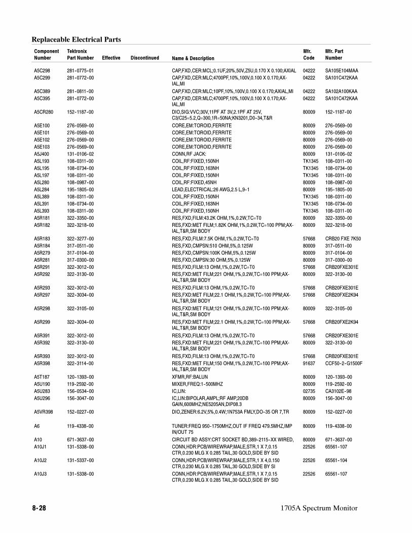
Replaceable Electrical Parts
8- 28 1705A Spectrum Monitor
Component
Number
Mfr. Part
Number
Mfr.
CodeName & DescriptionEffective Discontinued
Tektronix
Part Number
A5C298 281--0775--01 CAP,FXD,CER:MCL;0.1UF,20%,50V,Z5U,0.170 X 0.100;AXIAL 04222 SA105E104MAA
A5C299 281--0772--00 CAP,FXD,CER:MLC;4700PF,10%,100V,0.100 X 0.170;AX-IAL,MI
04222 SA101C472KAA
A5C389 281--0811--00 CAP,FXD,CER:MLC;10PF,10%,100V,0.100 X 0.170;AXIAL,MI 04222 SA102A100KAA
A5C395 281--0772--00 CAP,FXD,CER:MLC;4700PF,10%,100V,0.100 X 0.170;AX-IAL,MI
04222 SA101C472KAA
A5CR280 152--1187--00 DIO,SIG:VVC;30V,11PF AT 3V,2.1PF AT 25V,C3/C25=5.2,Q=300,1R=50NA;KN3201,D0--34,T&R
80009 152--1187--00
A5E100 276--0569--00 CORE,EM:TOROID,FERRITE 80009 276--0569--00
A5E101 276--0569--00 CORE,EM:TOROID,FERRITE 80009 276--0569--00
A5E102 276--0569--00 CORE,EM:TOROID,FERRITE 80009 276--0569--00
A5E103 276--0569--00 CORE,EM:TOROID,FERRITE 80009 276--0569--00
A5J400 131--0106--02 CONN,RF JACK: 80009 131--0106--02
A5L193 108--0311--00 COIL,RF:FIXED,150NH TK1345 108--0311--00
A5L195 108--0734--00 COIL,RF:FIXED,163NH TK1345 108--0734--00
A5L197 108--0311--00 COIL,RF:FIXED,150NH TK1345 108--0311--00
A5L280 108--0987--00 COIL,RF:FIXED,45NH 80009 108--0987--00
A5L284 195--1805--00 LEAD,ELECTRICAL:26 AWG,2.5 L,9--1 80009 195--1805--00
A5L389 108--0311--00 COIL,RF:FIXED,150NH TK1345 108--0311--00
A5L391 108--0734--00 COIL,RF:FIXED,163NH TK1345 108--0734--00
A5L393 108--0311--00 COIL,RF:FIXED,150NH TK1345 108--0311--00
A5R181 322--3350--00 RES,FXD,FILM:43.2K OHM,1%,0.2W,TC=T0 80009 322--3350--00
A5R182 322--3218--00 RES,FXD:MET FILM;1.82K OHM,1%,0.2W,TC=100 PPM;AX-IAL,T&R,SM BODY
80009 322--3218--00
A5R183 322--3277--00 RES,FXD,FILM:7.5K OHM,1%,0.2W,TC=T0 57668 CRB20 FXE 7K50
A5R184 317--0511--00 RES,FXD,CMPSN:510 OHM,5%,0.125W 80009 317--0511--00
A5R279 317--0104--00 RES,FXD,CMPSN:100K OHM,5%,0.125W 80009 317--0104--00
A5R281 317--0300--00 RES,FXD,CMPSN:30 OHM,5%,0.125W 80009 317--0300--00
A5R291 322--3012--00 RES,FXD,FILM:13 OHM,1%,0.2W,TC=T0 57668 CRB20FXE301E
A5R292 322--3130--00 RES,FXD:MET FILM;221 OHM,1%,0.2W,TC=100 PPM;AX-IAL,T&R,SM BODY
80009 322--3130--00
A5R293 322--3012--00 RES,FXD,FILM:13 OHM,1%,0.2W,TC=T0 57668 CRB20FXE301E
A5R297 322--3034--00 RES,FXD:MET FILM;22.1 OHM,1%,0.2W,TC=100 PPM;AX-IAL,T&R,SM BODY
57668 CRB20FXE2K94
A5R298 322--3105--00 RES,FXD:MET FILM;121 OHM,1%,0.2W,TC=100 PPM;AX-IAL,T&R,SM BODY
80009 322--3105--00
A5R299 322--3034--00 RES,FXD:MET FILM;22.1 OHM,1%,0.2W,TC=100 PPM;AX-IAL,T&R,SM BODY
57668 CRB20FXE2K94
A5R391 322--3012--00 RES,FXD,FILM:13 OHM,1%,0.2W,TC=T0 57668 CRB20FXE301E
A5R392 322--3130--00 RES,FXD:MET FILM;221 OHM,1%,0.2W,TC=100 PPM;AX-IAL,T&R,SM BODY
80009 322--3130--00
A5R393 322--3012--00 RES,FXD,FILM:13 OHM,1%,0.2W,TC=T0 57668 CRB20FXE301E
A5R398 322--3114--00 RES,FXD:MET FILM;150 OHM,1%,0.2W,TC=100 PPM;AX-IAL,T&R,SM BODY
91637 CCF50--2--G1500F
A5T187 120--1393--00 XFMR,RF:BALUN 80009 120--1393--00
A5U190 119--2592--00 MIXER,FREQ:1--500MHZ 80009 119--2592--00
A5U283 156--0534--00 IC,LIN: 02735 CA3102E--98
A5U296 156--3047--00 IC,LIN:BIPOLAR,AMPL;RF AMP,20DBGAIN,600MHZ;NE5205AN,DIP08.3
80009 156--3047--00
A5VR398 152--0227--00 DIO,ZENER:6.2V,5%,0.4W;1N753A FMLY,DO--35 OR 7,TR 80009 152--0227--00
A6 119--4338--00 TUNER:FREQ 950--1750MHZ,OUT IF FREQ 479.5MHZ,IMPIN/OUT 75
80009 119--4338--00
A10 671--3637--00 CIRCUIT BD ASSY:CRT SOCKET BD,389--2115--XX WIRED, 80009 671--3637--00
A10J1 131--5338--00 CONN,HDR:PCB/WIREWRAP,MALE,STR,1 X 7,0.15CTR,0.230 MLG X 0.285 TAIL,30 GOLD,SIDE BY SID
22526 65561--107
A10J2 131--5337--00 CONN,HDR:PCB/WIREWRAP,MALE,STR,1 X 4,0.150CTR,0.230 MLG X 0.285 TAIL,30 GOLD,SIDE BY SI
22526 65561--104
A10J3 131--5338--00 CONN,HDR:PCB/WIREWRAP,MALE,STR,1 X 7,0.15CTR,0.230 MLG X 0.285 TAIL,30 GOLD,SIDE BY SID
22526 65561--107
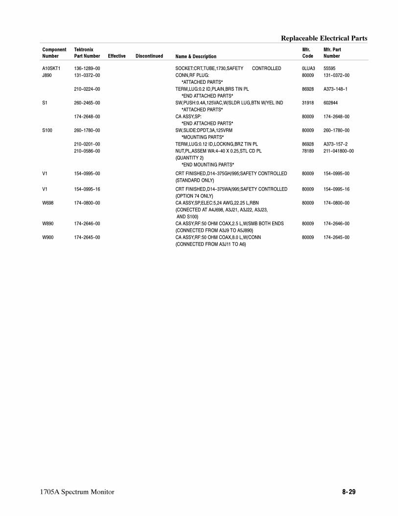
Replaceable Electrical Parts
1705A Spectrum Monitor 8- 29
Component
Number
Mfr. Part
Number
Mfr.
CodeName & DescriptionEffective Discontinued
Tektronix
Part Number
A10SKT1 136--1289--00 SOCKET:CRT,TUBE,1730,SAFETY CONTROLLED 0LUA3 55595
J890 131--0372--00 CONN,RF PLUG: 80009 131--0372--00
*ATTACHED PARTS*
210--0224--00 TERM,LUG:0.2 ID,PLAIN,BRS TIN PL 86928 A373--148--1
*END ATTACHED PARTS*
S1 260--2465--00 SW,PUSH:0.4A,125VAC,W/SLDR LUG,BTN W/YEL IND 31918 602844
*ATTACHED PARTS*
174--2648--00 CA ASSY,SP: 80009 174--2648--00
*END ATTACHED PARTS*
S100 260--1780--00 SW,SLIDE:DPDT,3A,125VRM 80009 260--1780--00
*MOUNTING PARTS*
210--0201--00 TERM,LUG:0.12 ID,LOCKING,BRZ TIN PL 86928 A373--157--2
210--0586--00 NUT,PL,ASSEM WA:4--40 X 0.25,STL CD PL 78189 211--041800--00
(QUANTITY 2)
*END MOUNTING PARTS*
V1 154--0995--00 CRT FINISHED,D14--375GH/995;SAFETY CONTROLLED 80009 154--0995--00
(STANDARD ONLY)
V1 154--0995--16 CRT FINISHED,D14--375WA/995;SAFETY CONTROLLED 80009 154--0995--16
(OPTION 74 ONLY)
W698 174--0800--00 CA ASSY,SP,ELEC:5,24 AWG,22.25 L,RBN 80009 174--0800--00
(CONECTED AT A4J698, A3J21, A3J22, A3J23,
AND S100)
W890 174--2646--00 CA ASSY,RF:50 OHM COAX,2.5 L,W/SMB BOTH ENDS 80009 174--2646--00
(CONNECTED FROM A3J9 TO A5J890)
W900 174--2645--00 CA ASSY,RF:50 OHM COAX,8.0 L,W/CONN 80009 174--2645--00
(CONNECTED FROM A3J11 TO A6)

Replaceable Electrical Parts
8- 30 1705A Spectrum Monitor

Diagrams/Circuit Board Illustrations

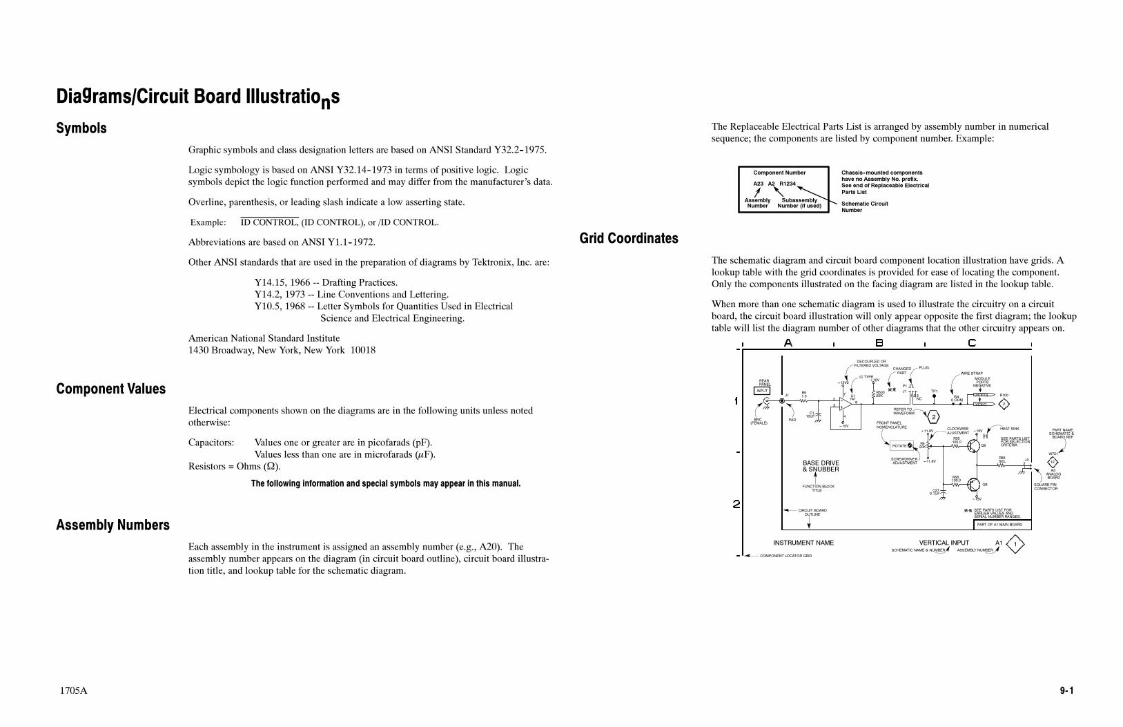
9- 11705A
Diagrams/Circuit Board Illustrations
Symbols
Graphic symbols and class designation letters are based on ANSI Standard Y32.2--1975.
Logic symbology is based on ANSI Y32.14--1973 in terms of positive logic. Logicsymbols depict the logic function performed and may differ from the manufacturer’s data.
Overline, parenthesis, or leading slash indicate a low asserting state.
Example: ID CONTROL, (ID CONTROL), or /ID CONTROL.
Abbreviations are based on ANSI Y1.1--1972.
Other ANSI standards that are used in the preparation of diagrams by Tektronix, Inc. are:
Y14.15, 1966 -- Drafting Practices.Y14.2, 1973 -- Line Conventions and Lettering.Y10.5, 1968 -- Letter Symbols for Quantities Used in Electrical
Science and Electrical Engineering.
American National Standard Institute1430 Broadway, New York, New York 10018
Component Values
Electrical components shown on the diagrams are in the following units unless notedotherwise:
Capacitors: Values one or greater are in picofarads (pF).Values less than one are in microfarads (F).
Resistors = Ohms (Ω).
The following information and special symbols may appear in this manual.
Assembly Numbers
Each assembly in the instrument is assigned an assembly number (e.g., A20). Theassembly number appears on the diagram (in circuit board outline), circuit board illustra-tion title, and lookup table for the schematic diagram.
The Replaceable Electrical Parts List is arranged by assembly number in numericalsequence; the components are listed by component number. Example:
Chassis--mounted componentshave no Assembly No. prefix.See end of Replaceable Electrical
Parts List
AssemblyNumber
Component Number
A23 A2 R1234
SubassemblyNumber (if used) Schematic Circuit
Number
Grid Coordinates
The schematic diagram and circuit board component location illustration have grids. Alookup table with the grid coordinates is provided for ease of locating the component.Only the components illustrated on the facing diagram are listed in the lookup table.
When more than one schematic diagram is used to illustrate the circuitry on a circuitboard, the circuit board illustration will only appear opposite the first diagram; the lookuptable will list the diagram number of other diagrams that the other circuitry appears on.
WIRE STRAP
MODULE
PLUG
P1 NEGATIVEPORTS
IC TYPE
CHANGEDPART
+12V
DECOUPLED ORFILTERED VOLTAGE
R50020K
+12V3REARPANEL
INPUT
BNC
J1
(FEMALE)PAD
FRONT PANELNOMENCLATURE
C110UF
2
36
7
4
U1741
---12V
R51.0
NC
ROTATE
H
HEAT SINK
2
REFER TOWAVEFORM
1 2 3
J1
R420K Q8
W40 OHM
+11.8V +15V
---11.8V
TP1
/VIDEO
(VIDEO)
R55100.0
CLOCKWISEAJUSTMENT
12J3
12
W751
A3ANALOGBOARD
SCHEMATIC &BOARD REF
PART NAME,
2
R100
R85SEL
SEE PARTS LISTFOR SELECTIONCRITERIA
SQUARE PINCONNECTOR
PART OF A1 MAIN BOARD
R56100.0
Q6
---15V
SEE PARTS LIST FOREARLIER VALUES ANDSERIAL NUMBER RANGES.
C270.1UF
SCREWDRIVERADJUSTMENT
CIRCUIT BOARDOUTLINE
& SNUBBER
BASE DRIVE
TITLEFUNCTION BLOCK
INSTRUMENT NAME
SCHEMATIC NAME & NUMBER ASSEMBLY NUMBER
VERTICAL INPUT 1A1
COMPONENT LOCATOR GRID

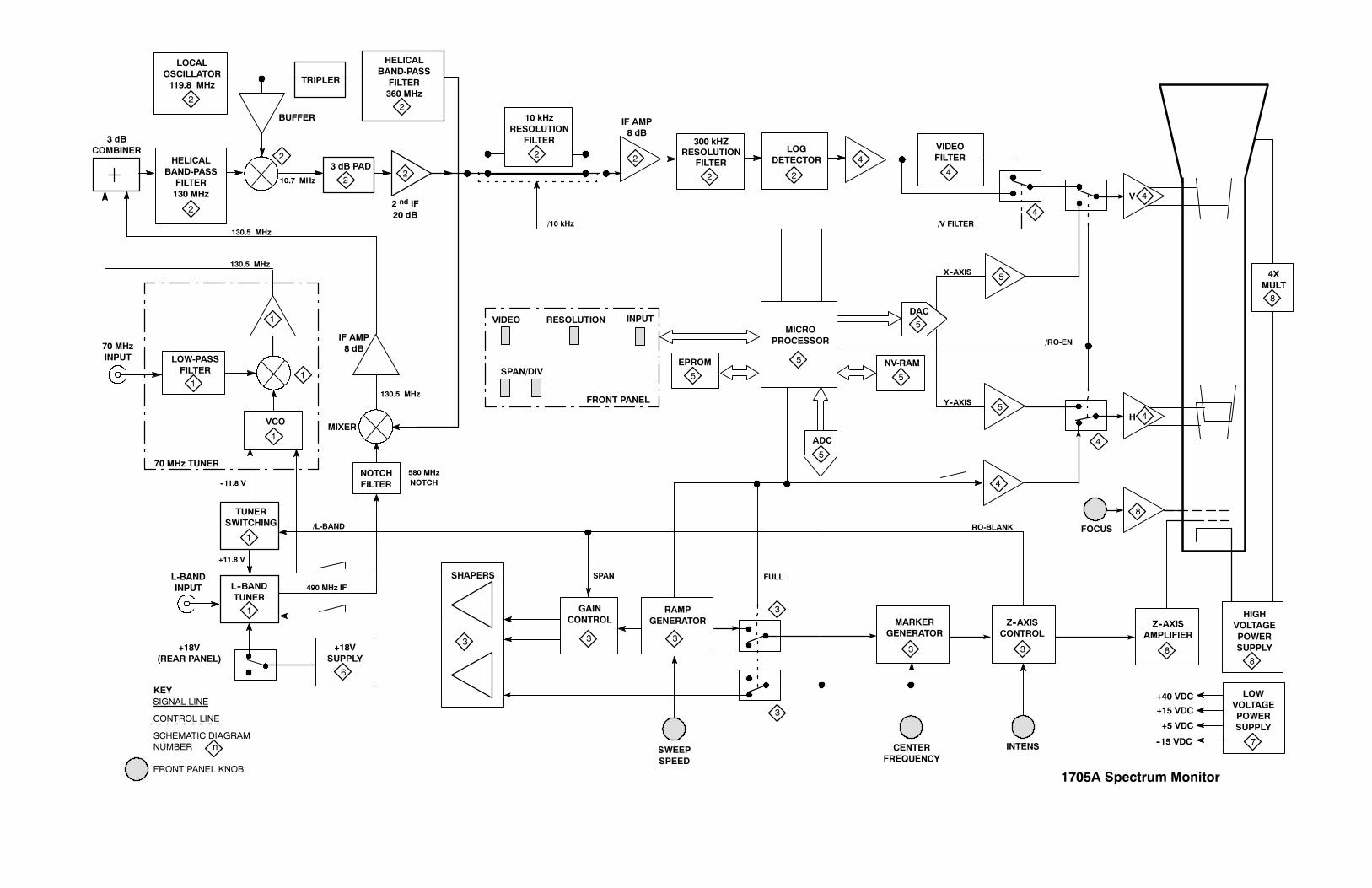
LOW-PASS
FILTER
3 dB PAD
10.7 MHz
NV-RAM
DAC
X--AXIS
+11.8 V
+18V
SUPPLY
10 kHz
RESOLUTION
FILTER
GAIN
CONTROL
--11.8 V
SPAN
LOW
VOLTAGE
POWER
SUPPLY
TUNER
SWITCHING
VCO
L--BAND
TUNER
RO-BLANK
300 kHZ
RESOLUTION
FILTER
130.5 MHz
BUFFER
TRIPLER
2 nd IF
20 dB
Y--AXIS
3 dB
COMBINER
HELICAL
BAND-PASS
FILTER
360 MHz
HELICAL
BAND-PASS
FILTER
130 MHz
LOCAL
OSCILLATOR
119.8 MHz
RAMP
GENERATOR MARKER
GENERATORZ--AXIS
AMPLIFIER
4X
MULT
V
H
FOCUS
INTENS
HIGH
VOLTAGE
POWER
SUPPLY
CONTROL LINE
SIGNAL LINE
KEY
SCHEMATIC DIAGRAM
NUMBER n
1705A Spectrum MonitorFRONT PANEL KNOB
7
+40 VDC
+15 VDC
+5 VDC
--15 VDC
Z--AXIS
CONTROL
CENTER
FREQUENCYSWEEP
SPEED
SHAPERS
+18V
(REAR PANEL)
VIDEO RESOLUTION INPUT
SPAN/DIV
FRONT PANEL
130.5 MHz
MICRO
PROCESSOR70 MHz
INPUT
IF AMP
8 dB
ADC
EPROM
LOG
DETECTOR
NOTCH
FILTER
130.5 MHz
IF AMP
8 dB
70 MHz TUNER
L-BAND
INPUT
/RO-EN
FULL
VIDEO
FILTER
1
8
580 MHz
NOTCH
MIXER
4
4
490 MHz IF
/L-BAND
/V FILTER/10 kHz
8
8
1
1
1
6
1
3 3 3
3
3
33
4
5
5
5
1
2
2
2
22
2
2 2
4
5
5
22
8
4
4
4
5
5
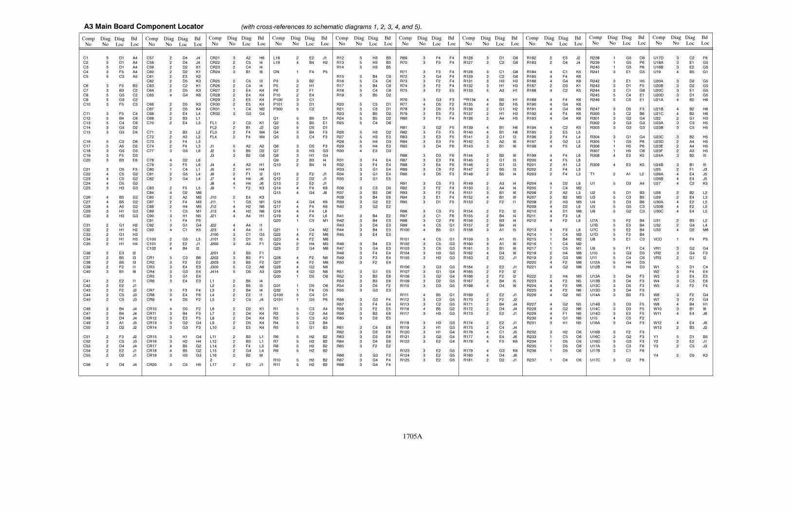
A3 Main Board Component Locator (with cross-references to schematic diagrams 1, 2, 3, 4, and 5).
CompNo
DiagNo
DiagLoc
BdLoc
CompNo
DiagNo
DiagLoc
BdLoc
CompNo
DiagNo
DiagLoc
BdLoc
CompNo
DiagNo
DiagLoc
BdLoc
CompNo
DiagNo
DiagLoc
BdLoc
CompNo
DiagNo
DiagLoc
BdLoc
1705A
C1 5 D1 A4
C2 5 D1 A4
C3 5 D1 A4
C4 3 F5 A4
C5 5 C3 A5
C6 3 F5 B3
C7 3 B3 C2
C8 5 G5 C2
C9 5 G5 C2
C10 3 F5 C3
C11 3 F5 C4
C12 5 B4 C6
C13 5 C4 C6
C14 3 G5 D2
C15 3 G5 D4
C16 5 C3 D6
C17 5 A5 D2
C18 3 G5 D3
C19 3 F5 D3
C20 3 B3 E6
C21 3 D5 F3
C22 4 C5 G2
C23 4 C5 G2
C24 4 D5 G2
C25 3 H3 G3
C26 4 B5 G2
C27 4 B5 G2
C28 4 A5 G2
C29 3 H1 G3
C30 3 H3 G3
C31 2 G1 H2
C32 2 H1 H2
C33 2 G1 H3
C34 2 H1 H3
C35 2 H1 H4
C36 2 E3 I2
C37 2 B5 I3
C38 2 B5 I3
C39 2 F2 I1
C40 3 B1 I6
C41 2 E2 I1
C42 2 E2 J1
C43 2 F2 J2
C44 2 C5 J3
C45 2 C5 J3
C46 2 B4 J4
C47 2 B4 J4
C48 2 D4 J4
C49 3 A1 J5
C50 2 D2 J2
C51 2 F3 J2
C52 2 C5 J3
C53 2 D4 J4
C54 2 E2 J1
C55 2 D2 J1
C56 2 D4 J4
C57 2 D4 J4
C58 2 D4 J4
C59 2 D2 K1
C60 2 D2 K1
C61 2 E3 K2
C62 2 D5 K3
C63 2 C2 K1
C64 2 D5 K3
C65 4 G4 K6
C66 2 D5 K3
C67 2 D5 K4
C68 2 E4 L4
C69 2 B3 L1
C70 2 E4 L3
C71 2 B3 L2
C72 2 A3 L2
C73 2 F4 L3
C74 2 F4 L3
C77 3 G5 L6
C78 4 D2 L6
C79 3 F5 L6
C80 1 C4 L1
C81 2 G5 L4
C82 2 G4 L4
C83 2 F5 L5
C84 4 D2 M6
C85 2 A2 M2
C87 2 F4 M3
C88 2 H4 M5
C89 1 C5 M1
C90 3 H1 N5
C91 1 F4 P5
C92 3 G1 G4
C93 4 C1 K5
C100 2 G5 L5
C101 2 E2 J1
C102 4 B4 I2
CR1 5 C3 B6
CR2 3 F2 E2
CR3 3 E4 E3
CR4 3 G3 E4
CR5 3 G1 E4
CR6 3 E4 E3
CR7 3 F3 F4
CR8 3 E4 F6
CR9 4 D5 F2
CR10 4 D5 F2
CR11 3 B4 F3
CR12 3 E3 F5
CR13 3 G2 G4
CR14 3 G3 F3
CR15 3 H1 G4
CR16 3 H2 H4
CR17 4 B5 G2
CR18 4 B5 G2
CR19 3 H3 G3
CR20 3 C5 H5
CR21 3 A2 H6
CR22 2 C5 I4
CR23 2 C4 I4
CR24 3 B1 I6
CR25 2 C5 I3
CR26 2 C4 I4
CR27 2 E4 K4
CR28 2 E4 K4
CR29 2 E5 K4
CR30 2 E5 K4
CR31 1 C4 M2
CR32 3 G3 G4
FL1 2 C2 K1
FL2 2 B1 J2
FL3 2 F4 M4
FL4 2 F4 M4
J1 5 A2 A2
J2 5 B5 D2
J3 3 B2 G6
J4 4 A3 H1
J5 2 H1 H4
J6 2 F1 I2
J7 4 H4 J6
J8 4 H4 J6
J9 1 F2 K3
J10 2 E4 K3
J11 1 G5 M1
J12 4 H2 N6
J13 4 H2 N6
J21 4 A4 H1
J22 4 A4 I1
J23 4 A4 I1
J100 3 C1 G5
J101 3 D1 I5
J200 3 A3 F1
J201 3 B3 F1
J202 3 B3 F1
J203 3 B3 F2
J300 5 C2 A6
J414 5 D5 A3
L1 2 B5 I4
L2 2 B5 I3
L3 2 B4 I4
L4 2 E2 I1
L5 2 C5 J4
L6 2 D2 K1
L7 2 D4 K4
L8 2 D4 K4
L9 2 D5 K4
L10 2 E5 K4
L11 2 B3 L1
L12 2 B3 L1
L14 2 F4 L3
L15 2 G4 L4
L16 2 B2 M
2
L17 2 E2 J1
L18 2 E2 J1
L19 4 B4 H2
ON 1 F4 P5
P3 3 B2
P5 2 H1
P6 2 F1
P10 2 E4
P100 3 C1
P101 3 D1
P300 5 C2
Q1 5 B5 D1
Q2 5 B5 E1
Q3 5 D5 D1
Q4 3 B4 F3
Q5 3 C4 F3
Q6 3 D5 F3
Q7 3 H3 G3
Q8 3 H1 G4
Q9 2 B3 I4
Q10 2 B4 I4
Q11 2 F2 J1
Q12 2 D2 J1
Q13 2 E2 J1
Q14 4 F4 K6
Q15 4 G4 J6
Q16 4 G4 K6
Q17 4 F4 K6
Q18 4 F4 L6
Q19 4 F4 L6
Q20 1 C5 M1
Q21 1 C4 M2
Q22 4 F2 M6
Q23 4 F2 M6
Q24 2 H4 M5
Q25 2 G4 M6
Q26 4 F2 N6
Q27 4 F2 M6
Q28 4 G2 N6
Q29 4 G2 N6
Q30 1 D5 O6
Q31 1 D5 O6
Q32 1 F4 O5
Q100 5 C4 D1
Q101 1 G5 P6
R1 5 C3 A4
R2 5 C2 A4
R3 5 C3 A3
R4 5 C3 B4
R5 5 G1 B3
R6 5 H2 B2
R7 5 H2 B2
R8 5 H2 B2
R9 5 H2 B2
R10 5 H2 B2
R11 5 H2 B2
R12 5 H3 B3
R13 5 H3 B3
R14 5 H3 B5
R15 5 B4 C6
R16 5 C4 C6
R17 5 B4 C6
R18 5 C4 C6
R19 5 B5 D2
R20 5 C5 D1
R21 5 C5 D1
R23 5 B5 D2
R24 5 B5 D2
R25 5 C4 D6
R26 5 H3 D2
R27 5 H3 E3
R28 5 H4 D3
R29 5 H4 E3
R30 4 E3 D3
R31 3 F4 E4
R32 3 F4 E4
R33 3 G1 E4
R34 3 G1 E4
R35 3 G1 E5
R36 3 C3 D5
R37 3 B3 D6
R38 3 B4 E6
R39 3 G2 E2
R40 3 G2 E2
R41 3 B4 E2
R42 3 B4 E3
R43 3 D4 E3
R44 3 B4 E3
R45 3 E4 E3
R46 3 B4 E3
R47 3 G4 E3
R48 3 F4 E4
R49 3 F3 E4
R50 3 F2 E4
R51 3 G1 E5
R52 3 B3 E6
R53 3 B3 E6
R54 3 D5 F2
R55 3 G3 E3
R56 3 G3 F4
R57 3 F4 E4
R58 3 F2 E5
R59 3 B3 E6
R60 3 D3 E5
R61 3 C4 E6
R62 3 D3 F6
R63 3 D3 E6
R64 3 D4 E6
R65 3 F2 E2
R66 3 G3 F3
R67 3 G4 F4
R68 3 G4 F4
R69 3 F4 F4
R70 3 F3 F4
R71 3 F3 F4
R72 3 G4 F4
R73 3 F2 F4
R74 3 F2 F4
R75 3 F2 E5
R76 3 G3 F3
R77 4 D5 F2
R78 3 D5 F3
R79 3 E5 F3
R80 3 F3 F4
R81 3 G2 F5
R82 3 F3 F5
R83 3 E3 F5
R84 3 E3 F5
R85 3 D4 F6
R86 3 D3 F6
R87 3 E3 F6
R88 3 E4 F6
R89 3 C5 F2
R90 3 D5 F3
R91 3 C5 F3
R92 3 F2 F4
R93 3 F2 F4
R94 3 E1 F4
R95 3 D1 F5
R96 3 C3 F5
R97 3 C1 F6
R98 3 C2 F6
R99 4 C5 G1
R100 4 B5 G1
R101 4 C5 G1
R102 3 C5 G3
R103 3 C5 G3
R104 3 H3 G3
R105 3 H3 G3
R106 3 G3 G3
R107 3 G1 G4
R108 3 G2 G4
R109 3 D2 G5
R110 3 D3 G5
R111 4 B5 G1
R112 3 C3 G5
R113 3 C2 G5
R116 4 B5 G2
R117 3 H3 G3
R118 3 H3 G3
R119 3 H1 G3
R120 3 H1 G4
R121 3 G2 G4
R122 3 E2 G4
R123 3 E2 G5
R124 3 E2 G5
R125 3 E2 G5
R126 3 D1 G6
R127 3 C2 G6
R128 3 C1 G6
R129 3 C2 G6
R131 3 H3 H3
R132 3 H1 H3
R133 5 A3 H1
**R134 4 B5 H1
R135 4 B2 H5
R136 2 G1 H2
R137 2 H1 H3
R138 2 A4 H5
R139 4 B1 H6
R140 4 B1 H6
R141 2 G1 I3
R142 3 A2 I6
R143 3 B1 I6
R144 3 B2 I6
R145 2 G1 I3
R146 2 G1 I3
R147 2 B5 I3
R148 2 B5 I4
R149 2 A3 I4
R150 2 A4 I4
R151 3 B1 I6
R152 4 B1 I6
R153 2 F2 I1
R154 2 F2 I2
R155 2 B4 I4
R156 2 B3 I4
R157 2 B4 I4
R158 3 A1 I5
R159 3 A1 I5
R160 3 A1 I6
R161 3 B1 I6
R162 4 D4 I6
R163 2 E2 J1
R164 2 E2 J1
R165 2 F2 I2
R166 2 F2 I2
R167 2 B4 I5
R168 4 D4 I6
R169 2 E2 J1
R170 2 F2 J2
R171 2 B4 J4
R172 2 D4 J4
R173 2 E2 J1
R174 2 E2 J1
R175 2 C4 J4
R176 4 C1 J5
R177 4 E4 J6
R178 4 F3 K6
R179 4 G3 K6
R180 4 D4 J6
R181 2 D2 J1
R182 2 E3 J2
R183 2 D4 J4
R184 4 C1 K5
R185 4 F4 K6
R186 4 G4 K6
R187 2 D3 K1
R188 4 C2 K5
R189 4 F4 K6
R190 4 G4 K6
R191 4 G4 K6
R192 4 F4 K6
R193 4 G4 K6
R194 4 C2 K5
R195 2 E5 L5
R196 2 F4 L4
R197 4 G2 L5
R198 4 F5 L6
R199 4 F4 L6
R200 4 F5 L6
R201 2 A1 L3
R202 2 F4 L3
R203 2 F4 L3
R204 4 D2 L6
R205 1 C4 M2
R206 2 A2 L3
R207 2 B2 M3
R208 2 H3 M5
R209 4 D2 L6
R210 4 D1 M6
R211 4 F3 L6
R212 4 F2 L6
R213 4 F3 L6
R214 1 C4 M2
R215 1 B4 M2
R216 1 C4 M2
R217 1 C5 M1
R218 2 H4 M6
R219 2 G3 M6
R220 4 F2 M6
R221 4 G2 M6
R222 2 H4 M5
R223 4 F2 N5
R224 4 F2 M6
R225 4 F2 N6
R226 4 G2 N5
R227 4 G2 N5
R228 4 G2 N6
R229 4 F1 N6
R230 4 G1 N6
R231 3 H1 N5
R232 3 H2 O6
R233 1 C5 O6
R234 1 D5 O5
R235 1 D5 O6
R236 1 D5 O6
R237 1 D4 O6
R238 1 G5 O6
R239 1 G5 P6
R240 1 G5 P6
R241 3 E1 G5
R242 3 E1 H5
R243 3 D1 F5
R244 3 C1 G6
R245 5 C4 E1
R246 5 C5 E1
R247 3 D5 F3
R300 5 C2 B6
R301 3 G2 G4
R302 3 G3 G3
R303 3 G3 G3
R304 3 G1 G4
R305 1 G5 P6
R306 1 H5 P6
R307 1 H5 O6
R308 4 E3 K5
R309 4 E3 K5
T1 2 A1 L2
U1 5 D3 A4
U2 5 D1 B3
U3 5 C3 B5
U4 5 D3 B6
U5 5 G5 C3
U6 5 G2 C3
U7A 5 F2 B4
U7B 5 E3 B4
U7C 5 E2 B4
U7D 5 F3 B4
U8 5 E1 C3
U9 5 F1 C4
U10 5 G3 D3
U11 5 C4 C6
U12A 5 H4 D3
U12B 5 H4 D3
U13A 3 D4 F3
U13B 3 D4 F3
U13C 3 D5 F3
U13D 3 D4 F3
U14A 3 B3 F5
U14B 3 D3 F5
U14C 3 D3 F5
U14D 3 E3 F5
U15 4 C5 F2
U16A 3 G4 F3
U16B 3 F2 F3
U16C 3 G2 F3
U16D 3 G3 F3
U17A 3 C3 F6
U17B 3 C1 F6
U17C 3 C2 F6
U17D 3 C2 F6
U18A 3 E1 G5
U18B 3 E2 G5
U19 4 B5 G1
U20A 3 D2 G5
U20B 3 D2 G5
U20C 3 E1 G5
U20D 3 D1 G5
U21A 4 B2 H6
U21B 4 B2 H6
U21C 4 B2 H6
U22 2 G1 H3
U23A 3 C3 H5
U23B 3 C5 H5
U23C 3 B2 H5
U23D 2 A4 H5
U23E 2 A4 H5
U23F 2 A3 H5
U24A 3 B2 I5
U24B 3 B1 I5
U25 2 F1 J3
U26A 4 E4 J5
U26B 4 E4 J5
U27 4 C2 K5
U28 2 B2 L2
U29 2 E4 L3
U30A 4 E2 L5
U30B 4 E2 L5
U30C 4 E4 L5
U31 2 B3 L2
U32 2 G4 L4
U33 4 D2 M6
VCO 1 F4 P5
VR1 3 G2 G4
VR2 3 G4 F3
VR3 2 G1 I2
W1 5 D1 C4
W2 3 F4 E4
W3 3 E4 E5
W4 3 C3 E6
W5 3 F2 F4
W6 3 F2 G4
W7 3 F2 G4
W8 4 B4 H1
W10 3 B1 I6
W11 4 E4 J6
W12 4 E4 J6
W13 2 B3 J2
Y1 5 D1 B5
Y2 2 E2 J1
Y3 2 C5 J3
Y4 2 D5 K3
CompNo
DiagNo
DiagLoc
BdLoc
CompNo
DiagNo
DiagLoc
BdLoc
CompNo
DiagNo
DiagLoc
BdLoc
CompNo
DiagNo
DiagLoc
BdLoc
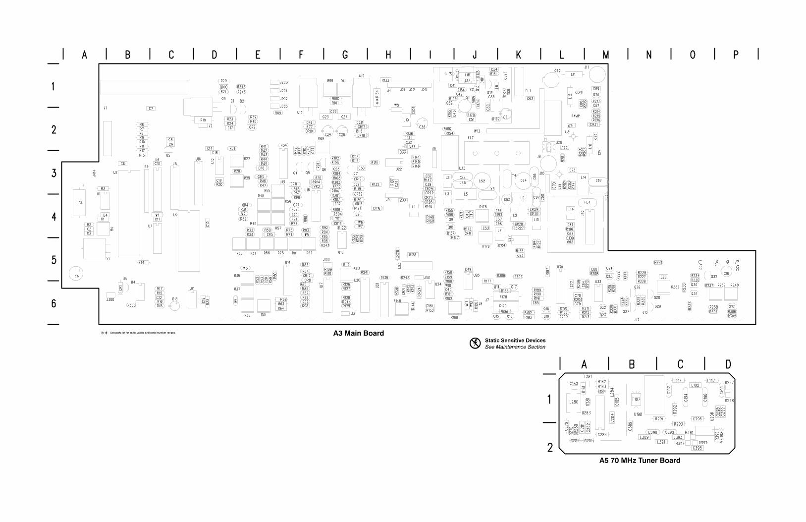
Static Sensitive Devices
See Maintenance Section
A3 Main Board
A5 70 MHz Tuner Board
See parts list for earier values and serial number ranges.
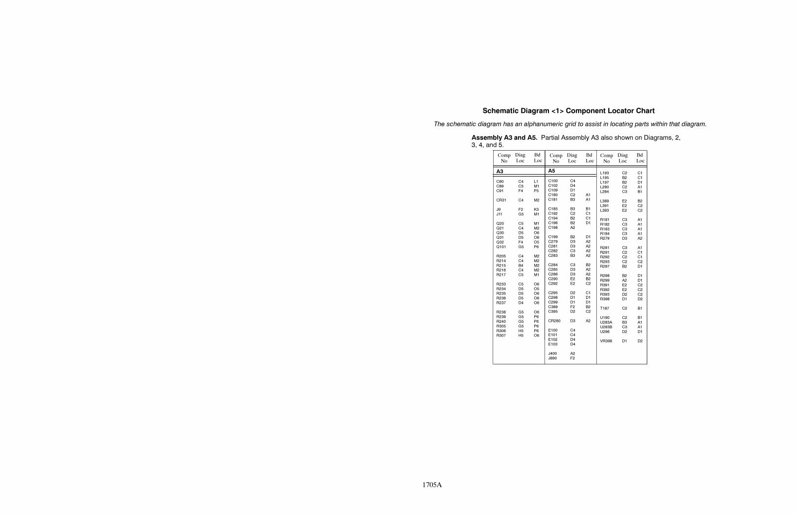
A3
C80 C4 L1
C89 C5 M1
C91 F4 P5
CR31 C4 M2
J9 F2 K3
J11 G5 M1
Q20 C5 M1
Q21 C4 M2
Q30 D5 O6
Q31 D5 O6
Q32 F4 O5
Q101 G5 P6
R205 C4 M2
R214 C4 M2
R215 B4 M2
R216 C4 M2
R217 C5 M1
R233 C5 O6
R234 D5 O5
R235 D5 O6
R236 D5 O6
R237 D4 O6
R238 G5 O6
R239 G5 P6
R240 G5 P6
R305 G5 P6
R306 H5 P6
R307 H5 O6
Schematic Diagram <1> Component Locator Chart
The schematic diagram has an alphanumeric grid to assist in locating parts within that diagram.
CompNo
Assembly A3 and A5. Partial Assembly A3 also shown on Diagrams, 2,3, 4, and 5.
BdLoc
DiagLoc
1705A
A5
C100 C4
C102 D4
C109 D1
C180 C2 A1
C181 B3 A1
C185 B3 B1
C192 C2 C1
C194 B2 C1
C196 B2 D1
C198 A2
C199 B2 D1
C279 D3 A2
C281 D3 A2
C282 C3 A2
C283 B3 A2
C284 C3 B2
C285 D3 A2
C286 D3 A2
C290 E2 B2
C292 E2 C2
C295 D2 C1
C298 D1 D1
C299 D1 D1
C389 F2 B2
C395 D2 C2
CR280 D3 A2
E100 C4
E101 C4
E102 D4
E103 D4
J400 A2
J890 F2
CompNo
BdLoc
DiagLoc
CompNo
BdLoc
DiagLoc
L193 C2 C1
L195 B2 C1
L197 B2 D1
L280 C2 A1
L284 C3 B1
L389 E2 B2
L391 E2 C2
L393 E2 C2
R181 C3 A1
R182 C3 A1
R183 C3 A1
R184 C3 A1
R279 D3 A2
R281 C3 A1
R291 C2 C1
R292 C2 C1
R293 C2 C2
R297 B2 D1
R298 B2 D1
R299 A2 D1
R391 E2 C2
R392 E2 C2
R393 D2 C2
R398 D1 D2
T187 C2 B1
U190 C2 B1
U283A B3 A1
U283B C3 A1
U296 D2 D1
VR398 D1 D2
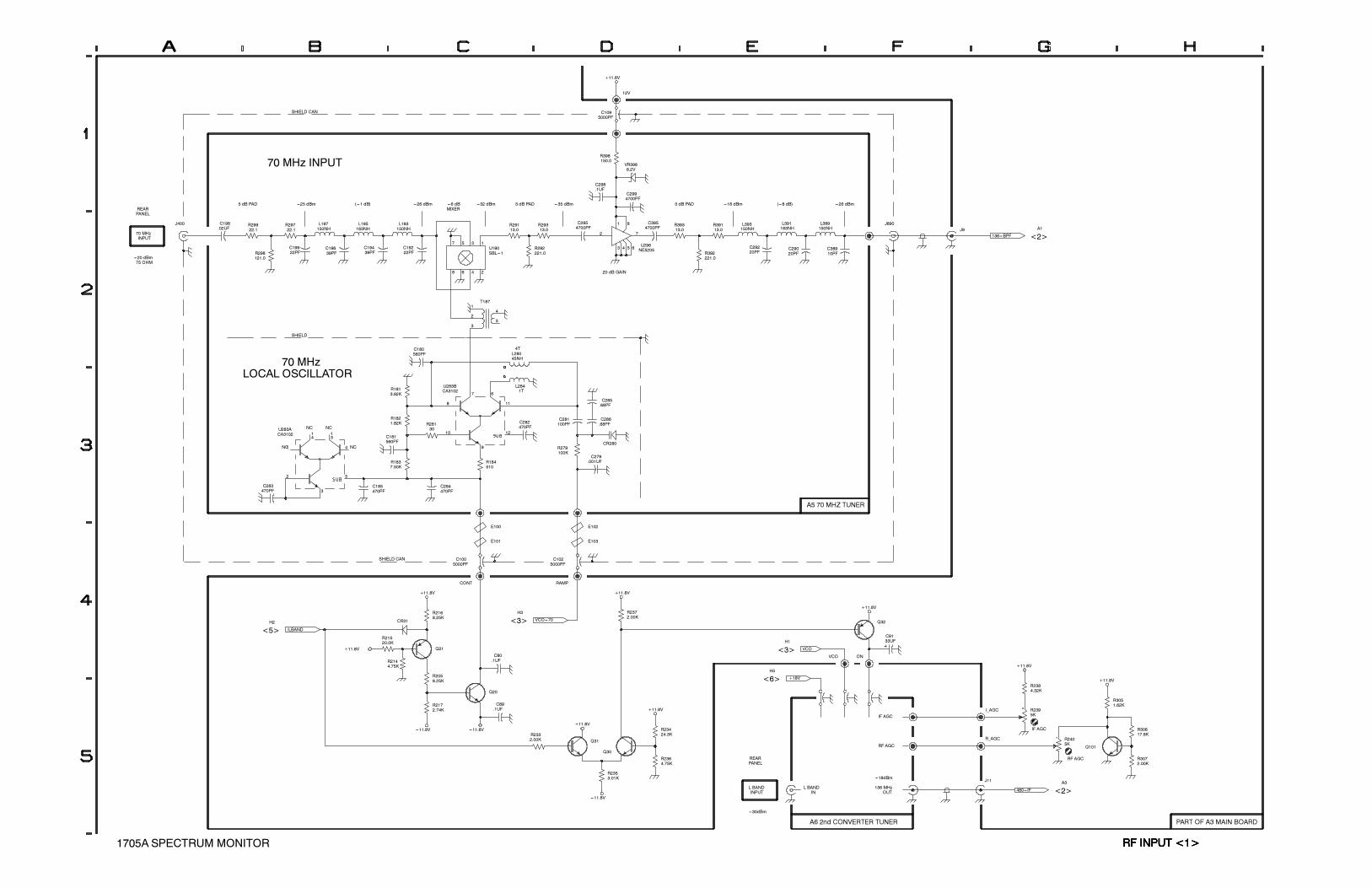
12V
+11.8V
C1095000PF
SHIELD CAN
REARPANEL
---25 dBm
70 MHz INPUT
5 dB PAD
J400
MIXER---26 dBm ---32 dBm---6 dB(---1 dB) 3 dB PAD ---35 dBm
C2994700PF
R398150.0
VR3986.2V
2 7
1
3
8
4 5 6U296NE5205
C298.1UF
3 dB PAD ---18 dBm (---8 dB) ---26 dBm
J890
<2>
A1
136---BPF
J9
C38910PF
C29020PF
R39313.0
R392221.0
L391163NH
L393150NH
C29220PF
R39113.0
L389150NH
20 dB GAIN
C2954700PF
R292221.0
R29313.0
C3954700PF
R29113.0
2468
7 5 3 1U190SBL---1
L195163NH
L193150NH
C19639PF
C19439PF
C19222PF
1
3
25
4
T187
SHIELD
C198.02UF
R29922.1
L197150NH
R298121.0
R29722.1
C19922PF
75 OHM
70 MHzINPUT
---20 dBm
LOCAL OSCILLATOR70 MHz
NCNC
NC1
14
4
3
13
2 5
U283ACA3102
NC
8
7
11
9
6
10 12
U283BCA3102
C181560PF
R184510
R1837.50K
R28130
R1821.82K
C180560PF
R1813.92K
C281100PFC282
470PF
4TL28045NH
1TL284
R279100K
CR280
C286.68PF
C285.68PF
A5 70 MHZ TUNER
RAMP
C279.001UF
C1025000PF
E102
E103
CONT
C185470PF
C284470PF
C1005000PF
SHIELD CAN
E100
E101
C283470PF
<5>
H2
/LBAND
R2058.25K
R2168.25K
Q21
CR31
R21520.0K
+11.8V
+11.8V
R2144.75K
Q20
<3>
H3
C80.1UF
R2372.00K
VCO---70
+11.8V
<3>
H1
<6>
H5
VCO
+18V
C9133UF
Q32
VCO ON
+11.8V
R2384.32K
+11.8V
<2>
A3
R2405K
RF AGC
R2395K
IF AGC
Q101
R3051.62K
R3072.00K
R30617.8K
480--- IF
+11.8V
---18dBm
136 MHzOUT
IF AGC
RF AGC
J11
I_AGC
R_AGC
REARPANEL
L BANDINPUT
L BANDIN
R2364.75K
R23424.3K
R2353.01K
R2332.00K
C89.1UF
Q30
Q31
+11.8V
+11.8V
---11.8V
---11.8V---11.8V
R2172.74K
1705A SPECTRUM MONITOR
---30dBm
A6 2nd CONVERTER TUNER
RF INPUT <1>RF INPUT <1>RF INPUT <1>RF INPUT <1>
PART OF A3 MAIN BOARD
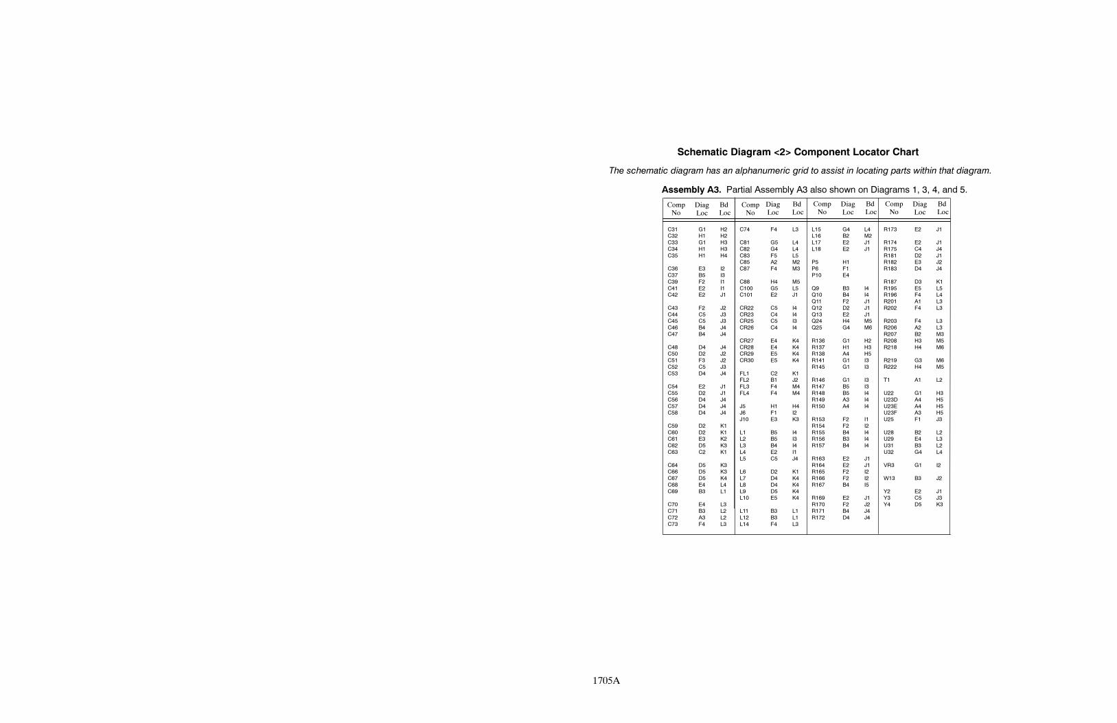
C31 G1 H2
C32 H1 H2
C33 G1 H3
C34 H1 H3
C35 H1 H4
C36 E3 I2
C37 B5 I3
C39 F2 I1
C41 E2 I1
C42 E2 J1
C43 F2 J2
C44 C5 J3
C45 C5 J3
C46 B4 J4
C47 B4 J4
C48 D4 J4
C50 D2 J2
C51 F3 J2
C52 C5 J3
C53 D4 J4
C54 E2 J1
C55 D2 J1
C56 D4 J4
C57 D4 J4
C58 D4 J4
C59 D2 K1
C60 D2 K1
C61 E3 K2
C62 D5 K3
C63 C2 K1
C64 D5 K3
C66 D5 K3
C67 D5 K4
C68 E4 L4
C69 B3 L1
C70 E4 L3
C71 B3 L2
C72 A3 L2
C73 F4 L3
C74 F4 L3
C81 G5 L4
C82 G4 L4
C83 F5 L5
C85 A2 M2
C87 F4 M3
C88 H4 M5
C100 G5 L5
C101 E2 J1
CR22 C5 I4
CR23 C4 I4
CR25 C5 I3
CR26 C4 I4
CR27 E4 K4
CR28 E4 K4
CR29 E5 K4
CR30 E5 K4
FL1 C2 K1
FL2 B1 J2
FL3 F4 M4
FL4 F4 M4
J5 H1 H4
J6 F1 I2
J10 E3 K3
L1 B5 I4
L2 B5 I3
L3 B4 I4
L4 E2 I1
L5 C5 J4
L6 D2 K1
L7 D4 K4
L8 D4 K4
L9 D5 K4
L10 E5 K4
L11 B3 L1
L12 B3 L1
L14 F4 L3
L15 G4 L4
L16 B2 M2
L17 E2 J1
L18 E2 J1
P5 H1
P6 F1
P10 E4
Q9 B3 I4
Q10 B4 I4
Q11 F2 J1
Q12 D2 J1
Q13 E2 J1
Q24 H4 M5
Q25 G4 M6
R136 G1 H2
R137 H1 H3
R138 A4 H5
R141 G1 I3
R145 G1 I3
R146 G1 I3
R147 B5 I3
R148 B5 I4
R149 A3 I4
R150 A4 I4
R153 F2 I1
R154 F2 I2
R155 B4 I4
R156 B3 I4
R157 B4 I4
R163 E2 J1
R164 E2 J1
R165 F2 I2
R166 F2 I2
R167 B4 I5
R169 E2 J1
R170 F2 J2
R171 B4 J4
R172 D4 J4
R173 E2 J1
R174 E2 J1
R175 C4 J4
R181 D2 J1
R182 E3 J2
R183 D4 J4
R187 D3 K1
R195 E5 L5
R196 F4 L4
R201 A1 L3
R202 F4 L3
R203 F4 L3
R206 A2 L3
R207 B2 M3
R208 H3 M5
R218 H4 M6
R219 G3 M6
R222 H4 M5
T1 A1 L2
U22 G1 H3
U23D A4 H5
U23E A4 H5
U23F A3 H5
U25 F1 J3
U28 B2 L2
U29 E4 L3
U31 B3 L2
U32 G4 L4
VR3 G1 I2
W13 B3 J2
Y2 E2 J1
Y3 C5 J3
Y4 D5 K3
Schematic Diagram <2> Component Locator Chart
CompNo
The schematic diagram has an alphanumeric grid to assist in locating parts within that diagram.
DiagLoc
BdLoc
CompNo
CompNo
DiagLoc
BdLoc
CompNo
DiagLoc
BdLoc
Assembly A3. Partial Assembly A3 also shown on Diagrams 1, 3, 4, and 5.
BdLoc
DiagLoc
1705A
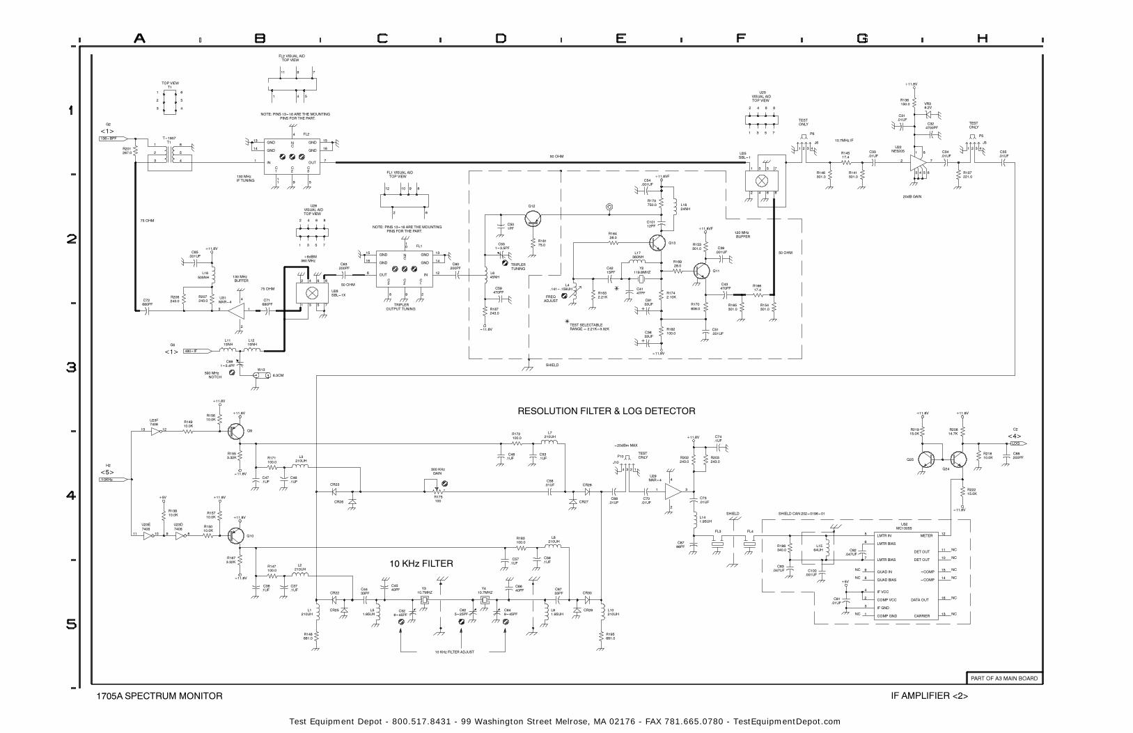
R136150.0
+11.8V
VISUAL AIDU25
TOP VIEW
7911
FL2 VISUAL AID
1 6
TOP VIEWT1
<1>
G2
R201267.0
136---BPF
NOTE: PINS 13---16 ARE THE MOUNTINGPINS FOR THE PART.
2
3 4
5
130 MHzIF TUNING
61
3 4
2 5
T1T---1907
C1
11
C2
9
C3
5
IN1
OUT7
GND15
GND16
GND13
GND14
NC
4 FL2
1 4 5
FL1 VISUAL AIDTOP VIEW
50 OHM
C54.001UF
+11.8VF
1 3 5 7
TESTONLY
2 4 6 8
TOP VIEW
2 4 6 8
7531
U25SBL---1
1 2 3 4
J6
P6
6.2V
10.7MHz IF
R146301.0
R141301.0
R14517.4
C33.01UF
C324700PF
C31.01UF
C34.01UF
2 7
1
3
8
4 5 6
U22NE5205
VR3
TESTONLY
R137221.0
C35.01UF
1 2 3 4
J5
P5
20dB GAIN
120 MHzBUFFER
50 OHM
C39.001UF
Q11
R153301.0
+11.8VF
R16928.0
R16428.0
Q13
Y2119.8MHZ
C4215PF
L4.141--- .159UH
R173750.0
L17360NH
C10112PF
L1824NH
6
89
TRIPLERTUNING
R18175.0C55
1---3.5PF
C60200PF
C501PF
L645NH
Q12
2 4 6 8
VISUAL AID
NOTE: PINS 13---16 ARE THE MOUNTINGPINS FOR THE PART.
2
1012
TOP VIEW
+6dBM360 MHz
1 3 5 7
U28
C63200PF
2 4 6 8
7531
U28SBL---1X
GND13
GND14
GND15
GND16
C1
2
C2
9
C3
8
OUT6
IN12
NC
10 FL1
130 MHzBUFFER
75 OHM
L16505NH
C85.001UF
+11.8V
<1>
G5
590 MHz
75 OHM
C72680PF
C71680PF
13
4
2
U31MAR---4
W13
6.3CM
L1215NH
R206243.0
R207243.0
C691---5.4PF
L1115NH
480--- IF
50 OHM
TRIPLEROUTPUT TUNING R187
243.0
C59470PF
---11.8V
FREQADJUST
SHIELD
C4147PF
R182100.0
R1742.10K
C6133UF
C3633UF
---11.8V
TEST SELECTABLERANGE = 2.21K---3.32K
R1632.21K
C43470PF
R165301.0
R16617.4
R154301.0
R170806.0
C51.001UF
<4>
C2R20814.7K
R21810.0K
C88200PF
LOG
+11.8V
R21915.0K
Q25
Q24
+11.8V
R203243.0
R202243.0
C74.1UF
+11.8V
---20dBm MAX
TESTONLY
1234
J10
P10
300 KHz
RESOLUTION FILTER & LOG DETECTOR
R172100.0
L7210UH
C48.1UF
C53.1UFL3
210UH
NOTCH
R15610.0K
13 12
U23F7406
Q9
R171100.0
R1553.32K
R14910.0K
+11.8V
+11.8V
---11.8V
H2
<5>
/10KHz
11 10
U23E7406
9 8
U23D7406
R1673.32K
Q10
R15710.0K
R15010.0K
R13810.0K
C47.1UF
+11.8V
+5V +11.8V
C46.1UF
CR23
CR26
GAIN
R183100.0
R175100
C57.1UF
C56.1UF
1 3
4
2
U29MAR---4
CR27
L8210UH
C58.01UF CR28
C68.01UF
C70.01UF
SHIELD SHIELD CAN 202---0196---01L141.95UH
C8798PF R196
340.0
C73.01UF
FL3 FL4
C83.047UF
NC
NC
LMTR IN5
LMTR BIAS6
LMTR BIAS7
QUAD IN9
QUAD BIAS8
METER12
DET OUT11
DET OUT10
+COMP15
---COMP14
IF VCC4
COMP VCC2
IF GND3
COMP GND1
CARRIER13
DATA OUT16
U32MC13055
C82.047UF
L1564UH
R22215.0K
---11.8V
NC
NC
NC
NCNC
NC
NC
C81.01UF
C100.001UF
+5V
CR29 L10210UH
R195681.0
C6733PF CR30
10 KHz FILTER ADJUST
L91.95UH
C625---25PF
C6640PF
C529---45PF
Y310.7MHZ
Y410.7MHZ
C649---45PF
10 KHz FILTER
CR25
CR22
L1210UH
R148681.0
L2210UH
C37.1UF
L51.95UH
C4433PF
C4540PF
R147100.0
C38.1UF
---11.8V
1705A SPECTRUM MONITOR IF AMPLIFIER <2>
PART OF A3 MAIN BOARD
Test Equipment Depot - 800.517.8431 - 99 Washington Street Melrose, MA 02176 - FAX 781.665.0780 - TestEquipmentDepot.com
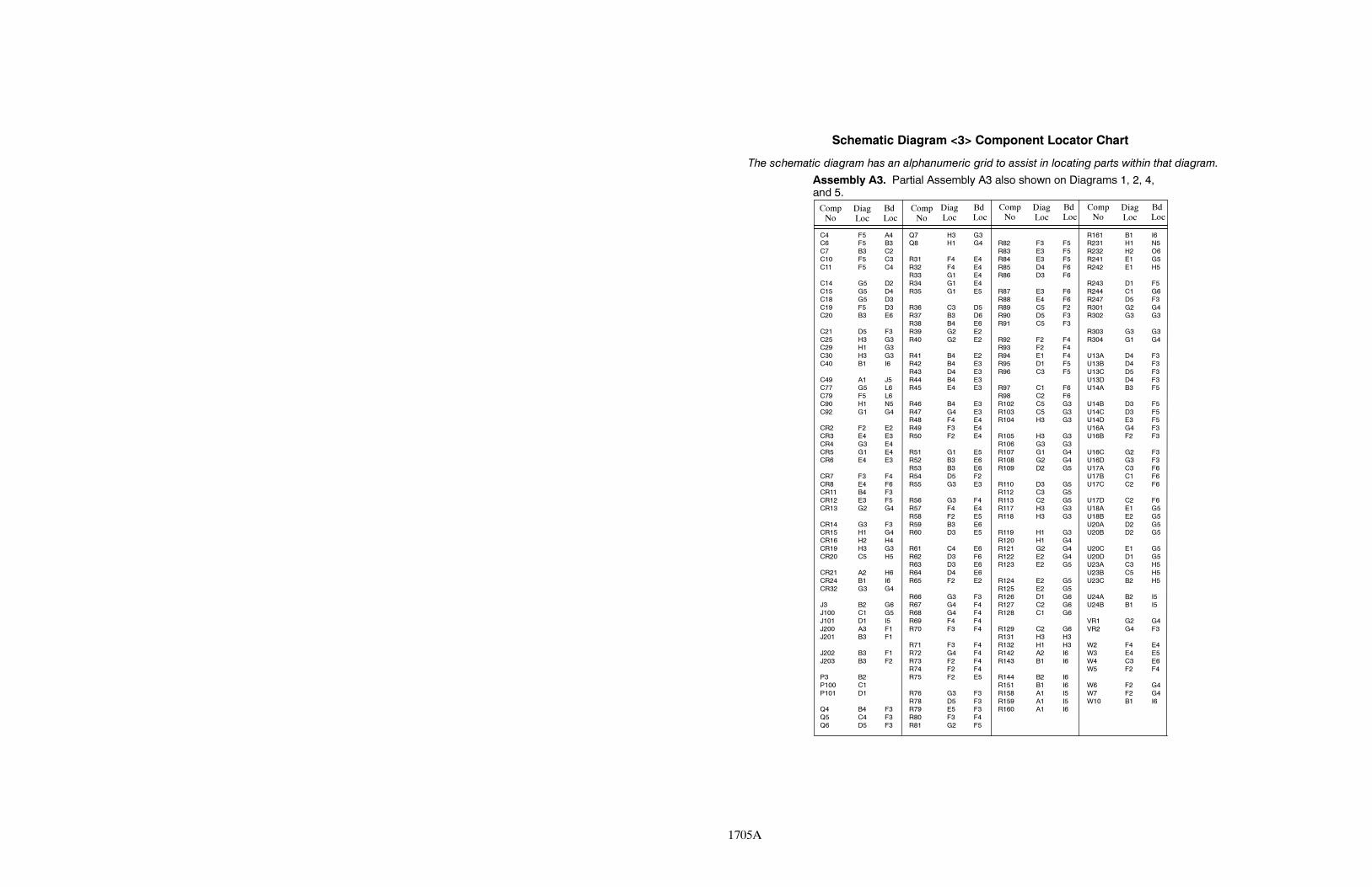
C4 F5 A4
C6 F5 B3
C7 B3 C2
C10 F5 C3
C11 F5 C4
C14 G5 D2
C15 G5 D4
C18 G5 D3
C19 F5 D3
C20 B3 E6
C21 D5 F3
C25 H3 G3
C29 H1 G3
C30 H3 G3
C40 B1 I6
C49 A1 J5
C77 G5 L6
C79 F5 L6
C90 H1 N5
C92 G1 G4
CR2 F2 E2
CR3 E4 E3
CR4 G3 E4
CR5 G1 E4
CR6 E4 E3
CR7 F3 F4
CR8 E4 F6
CR11 B4 F3
CR12 E3 F5
CR13 G2 G4
CR14 G3 F3
CR15 H1 G4
CR16 H2 H4
CR19 H3 G3
CR20 C5 H5
CR21 A2 H6
CR24 B1 I6
CR32 G3 G4
J3 B2 G6
J100 C1 G5
J101 D1 I5
J200 A3 F1
J201 B3 F1
J202 B3 F1
J203 B3 F2
P3 B2
P100 C1
P101 D1
Q4 B4 F3
Q5 C4 F3
Q6 D5 F3
Q7 H3 G3
Q8 H1 G4
R31 F4 E4
R32 F4 E4
R33 G1 E4
R34 G1 E4
R35 G1 E5
R36 C3 D5
R37 B3 D6
R38 B4 E6
R39 G2 E2
R40 G2 E2
R41 B4 E2
R42 B4 E3
R43 D4 E3
R44 B4 E3
R45 E4 E3
R46 B4 E3
R47 G4 E3
R48 F4 E4
R49 F3 E4
R50 F2 E4
R51 G1 E5
R52 B3 E6
R53 B3 E6
R54 D5 F2
R55 G3 E3
R56 G3 F4
R57 F4 E4
R58 F2 E5
R59 B3 E6
R60 D3 E5
R61 C4 E6
R62 D3 F6
R63 D3 E6
R64 D4 E6
R65 F2 E2
R66 G3 F3
R67 G4 F4
R68 G4 F4
R69 F4 F4
R70 F3 F4
R71 F3 F4
R72 G4 F4
R73 F2 F4
R74 F2 F4
R75 F2 E5
R76 G3 F3
R78 D5 F3
R79 E5 F3
R80 F3 F4
R81 G2 F5
R82 F3 F5
R83 E3 F5
R84 E3 F5
R85 D4 F6
R86 D3 F6
R87 E3 F6
R88 E4 F6
R89 C5 F2
R90 D5 F3
R91 C5 F3
R92 F2 F4
R93 F2 F4
R94 E1 F4
R95 D1 F5
R96 C3 F5
R97 C1 F6
R98 C2 F6
R102 C5 G3
R103 C5 G3
R104 H3 G3
R105 H3 G3
R106 G3 G3
R107 G1 G4
R108 G2 G4
R109 D2 G5
R110 D3 G5
R112 C3 G5
R113 C2 G5
R117 H3 G3
R118 H3 G3
R119 H1 G3
R120 H1 G4
R121 G2 G4
R122 E2 G4
R123 E2 G5
R124 E2 G5
R125 E2 G5
R126 D1 G6
R127 C2 G6
R128 C1 G6
R129 C2 G6
R131 H3 H3
R132 H1 H3
R142 A2 I6
R143 B1 I6
R144 B2 I6
R151 B1 I6
R158 A1 I5
R159 A1 I5
R160 A1 I6
R161 B1 I6
R231 H1 N5
R232 H2 O6
R241 E1 G5
R242 E1 H5
R243 D1 F5
R244 C1 G6
R247 D5 F3
R301 G2 G4
R302 G3 G3
R303 G3 G3
R304 G1 G4
U13A D4 F3
U13B D4 F3
U13C D5 F3
U13D D4 F3
U14A B3 F5
U14B D3 F5
U14C D3 F5
U14D E3 F5
U16A G4 F3
U16B F2 F3
U16C G2 F3
U16D G3 F3
U17A C3 F6
U17B C1 F6
U17C C2 F6
U17D C2 F6
U18A E1 G5
U18B E2 G5
U20A D2 G5
U20B D2 G5
U20C E1 G5
U20D D1 G5
U23A C3 H5
U23B C5 H5
U23C B2 H5
U24A B2 I5
U24B B1 I5
VR1 G2 G4
VR2 G4 F3
W2 F4 E4
W3 E4 E5
W4 C3 E6
W5 F2 F4
W6 F2 G4
W7 F2 G4
W10 B1 I6
Schematic Diagram <3> Component Locator Chart
CompNo
The schematic diagram has an alphanumeric grid to assist in locating parts within that diagram.
DiagLoc
BdLoc
CompNo
CompNo
DiagLoc
BdLoc
CompNo
DiagLoc
BdLoc
Assembly A3. Partial Assembly A3 also shown on Diagrams 1, 2, 4,and 5.
BdLoc
DiagLoc
1705A
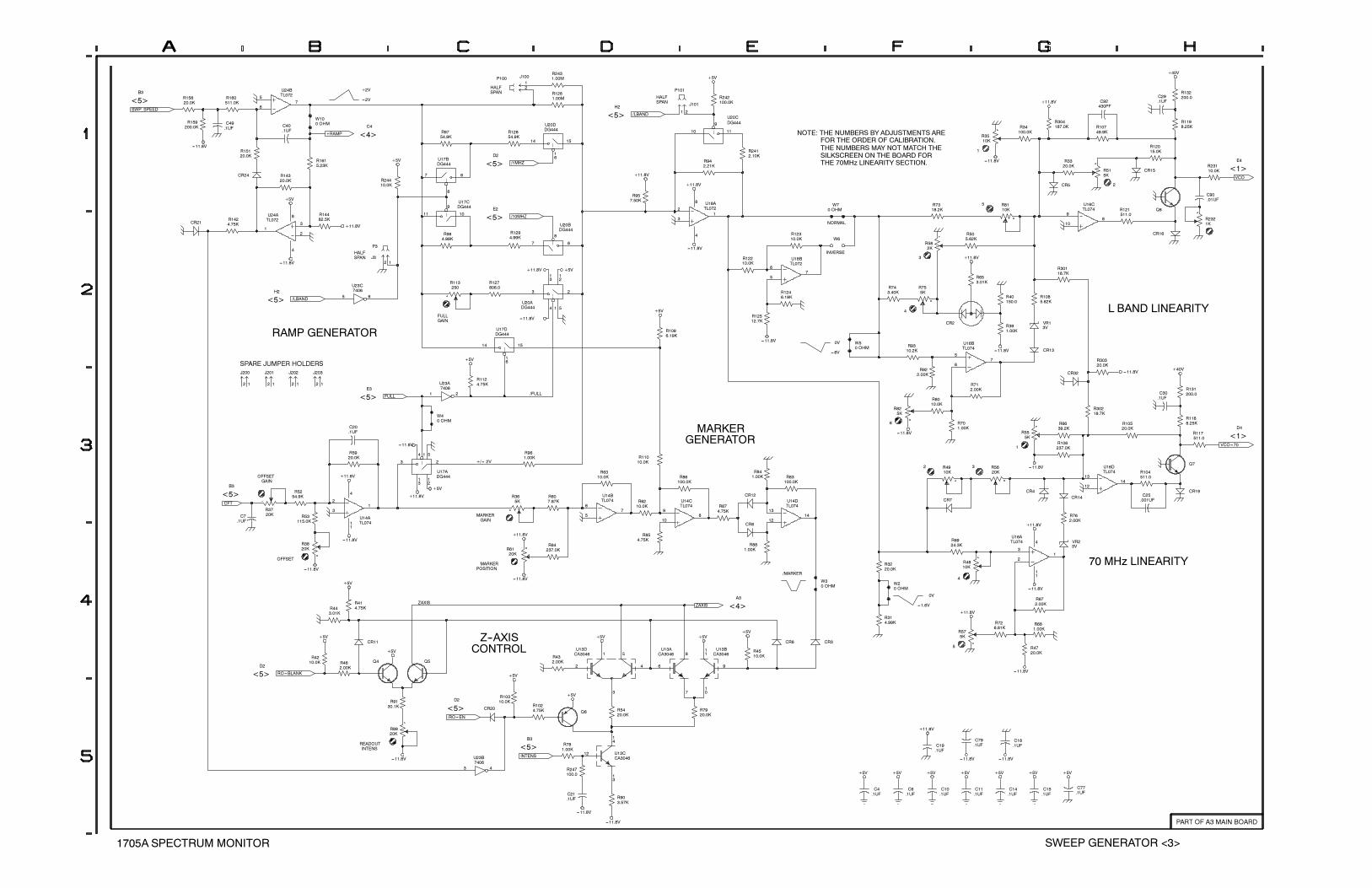
C29.1UF
R1198.25K
R132200.0
+40V
C92430PF
R304187.0K
+11.8V
1 2
J101
R242100.0K
P101
+5V
H2
HALFSPAN
R1261.00M
R2431.00M
12
J100P100
/LBAND
+2V
---2V
HALFSPAN
R159200.0K
R160511.0K
R15820.0K
5
67
U24BTL072
W100 OHM
<5>
B3
SWP_SPEED
R1615.23K
R14482.5K
R14320.0K
R15120.0K
C40.1UF
R1424.75KCR21
CR24
C49.1UF
+RAMP
+5V
---11.8V
3
21
8
4
U24ATL072
<4>
C4
<5>
<5>
R24410.0K
1011
9U17CDG444
R9754.9K
7 6
8
U17BDG444
+5V
+11.8V
D2
E2
<5>
R957.50K
R12854.9K
1514
16
U20DDG444
/1MHZ
/10MHZ
+11.8V
FOR THE ORDER OF CALIBRATION.
THE NUMBERS MAY NOT MATCH THE
NOTE: THE NUMBERS BY ADJUSTMENTS ARE
SILKSCREEN ON THE BOARD FOR
THE 70MHz LINEARITY SECTION.
10 11
9
U20CDG444
R942.21K
R2412.10K
+11.8V
2
31
8
4
U18ATL072
1
5W70 OHM
NORMAL
R7318.2K
2
R8110K
9
108
U16CTL074 R121
511.0
CR5
CR15R515K
R3320.0K
R12015.0K
R3510K
R34100.0K
R10749.9K
---11.8V
<1>
E4
Q8
R2321K
C90.01UF
R23110.0K
VCO
CR16
L BAND LINEARITY
3V
R1085.62K
VR1R391.00K
R40150.0
R30118.7K
---11.8V
4
3
W50 OHM
CR2
R653.01K
R755K
R743.40K
R505.62K
R582K
W6
INVERSE+11.8V
R12512.7K
R1246.19K
R12210.0K
R12310.0K
+5V
---11.8V
---11.8V
6
57
U18BTL072
R1096.19K
R1294.99K
23
1
12
13
4 5
U20ADG444
7 6
8
U20BDG444
1514
16
U17DDG444
---11.8V
+11.8V +5V
FULLGAIN
HALFSPAN
5 6
U23C7406
R113250
R984.99K
R127806.0
12J3
P3
RAMP GENERATOR
<5>
H2
/LBAND
---11.8V
SPARE JUMPER HOLDERS
12
J200
12
J201
12
J202
12
J203
<5>
E3
R1124.75K
W40 OHM
1 2
U23A7406
C20.1UF
FULL
+5V
---11.8V
R11010.0K
/FULL
MARKERGENERATOR
6
0V
---8V
R701.00K
R825K
R8010.0K
R712.00K
R922.00K
5
67
U16BTL074
R9310.2K
---11.8V
1R106237.0K
R6639.2K
R555K
R10520.0K
CR13
R30218.7K
R30320.0K
CR32 ---11.8V
<1>
D4
R1188.25K
Q7
R117511.0
R131200.0C30
.1UF
VCO---70
+40V
CR19
70 MHz LINEARITY
3V3
21
4
11
U16ATL074 VR2
CR4C25.001UF
+11.8V
---11.8V
13
1214
U16DTL074 R104
511.0
CR14
R762.00K
32
R3220.0K
R4810K
R6924.3K
CR7
R4910K
R5620K
9
108
U14CTL074
R86100.0K
R874.75K
CR12
CR8
R881.00K
13
1214
U14DTL074
R841.00K R83
100.0K
R607.87K
R64237.0KR61
20K
6
57
U14BTL074 R62
10.0K
R854.75K
R365K
R6310.0K
R961.00K
+11.8V
---11.8V
MARKERPOSITION
GAINMARKER
+/--- 2V
R5920.0K
2
31
4
11
U14ATL074
23
1
12
13
4 5
U17ADG444+11.8V
---11.8V
+11.8V
+5V
OFFSET
<5>
GAINOFFSET
B3
C7.1UF
R5254.9K
R3820K
R53115.0K
CFT
---11.8V
R3720K
<5>
D2
R4210.0K
R443.01K
RO---BLANK
+5V
CONTROLZ--AXIS
CR11
Q4 Q5R462.00K
R414.75K
ZAXIS
+5V
+5V
R432.00K
+5V
+5V
1
2
3
4
5U13DCA3046
/MARKER
<4>
A3
W30 OHM
CR6 CR3
R4510.0K
ZAXIS
+5V+5V
11
9
10
U13BCA30468
6
7
U13ACA3046
5
0V
---1.6V
4
R314.99K
W20 OHM
R575K
+11.8V
R726.81K
R681.00K
R672.00K
---11.8V
---11.8V
R4720.0K
+5V +5V +5V
---11.8V
C14.1UF
C15.1UF
C77.1UF
C18.1UF
+11.8V
+5V +5V+5V+5V
---11.8V
C79.1UF
C10.1UF
C11.1UF
C6.1UF
C4.1UF
C19.1UF
R7920.0K
<5>
B3
R903.57K
Q6 R5420.0K
R781.00K
C21.1UF
R1024.75K
R10310.0K
R247100.0
INTENS
+5V
14
12
13
U13CCA3046
INTENSREADOUT
<5>
D2
CR20
3 4
U23B7406
R8920K
R9130.1K
/RO---EN
---11.8V
1705A SPECTRUM MONITOR
---11.8V
---11.8V
SWEEP GENERATOR <3>
PART OF A3 MAIN BOARD
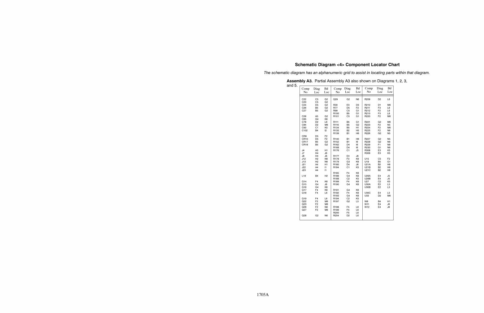
C22 C5 G2
C23 C5 G2
C24 D5 G2
C26 B5 G2
C27 B5 G2
C28 A5 G2
C65 G4 K6
C78 D2 L6
C84 D2 M6
C93 C1 K5
C102 B4 I2
CR9 D5 F2
CR10 D5 F2
CR17 B5 G2
CR18 B5 G2
J4 A3 H1
J7 H4 J6
J8 H4 J6
J12 H2 N6
J13 H2 N6
J21 A4 H1
J22 A4 I1
J23 A4 I1
L19 B4 H2
Q14 F4 K6
Q15 G4 J6
Q16 G4 K6
Q17 F4 K6
Q18 F4 L6
Q19 F4 L6
Q22 F2 M6
Q23 F2 M6
Q26 F2 N6
Q27 F2 M6
Q28 G2 N6
Q29 G2 N6
R30 E3 D3
R77 D5 F2
R99 C5 G1
R100 B5 G1
R101 C5 G1
R111 B5 G1
R116 B5 G2
R134 B5 H1
R135 B2 H5
R139 B1 H6
R140 B1 H6
R152 B1 I6
R162 D4 I6
R168 D4 I6
R176 C1 J5
R177 E4 J6
R178 F3 K6
R179 G3 K6
R180 D4 J6
R184 C1 K5
R185 F4 K6
R186 G4 K6
R188 C2 K5
R189 F4 K6
R190 G4 K6
R191 G4 K6
R192 F4 K6
R193 G4 K6
R194 C2 K5
R197 G2 L5
R198 F5 L6
R199 F4 L6
R200 F5 L6
R204 D2 L6
R209 D2 L6
R210 D1 M6
R211 F3 L6
R212 F2 L6
R213 F3 L6
R220 F2 M6
R221 G2 M6
R223 F2 N5
R224 F2 M6
R225 F2 N6
R226 G2 N5
R227 G2 N5
R228 G2 N6
R229 F1 N6
R230 G1 N6
R308 E3 K5
R309 E3 K5
U15 C5 F2
U19 B5 G1
U21A B2 H6
U21B B2 H6
U21C B2 H6
U26A E4 J5
U26B E4 J5
U27 C2 K5
U30A E2 L5
U30B E2 L5
U30C E4 L5
U33 D2 M6
W8 B4 H1
W11 E4 J6
W12 E4 J6
Schematic Diagram <4> Component Locator Chart
CompNo
The schematic diagram has an alphanumeric grid to assist in locating parts within that diagram.
DiagLoc
BdLoc
CompNo
CompNo
DiagLoc
BdLoc
Assembly A3. Partial Assembly A3 also shown on Diagrams 1, 2, 3,and 5.
BdLoc
DiagLoc
1705A
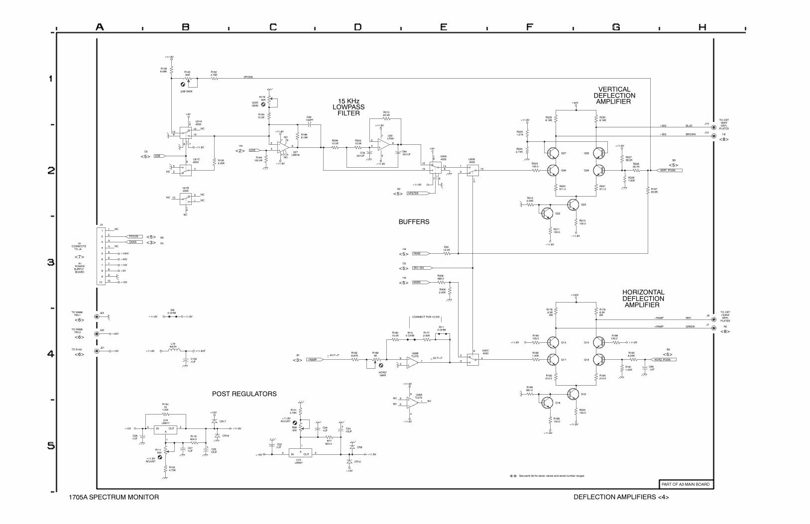
R1399.09K
+11.8V
2dB GAIN
R14050K
12
13146
11
16
78
U21A4053
+5V
GAINVERT
NC
R18410.0K
R17650K
R1524.75K
VPOSN
FILTERLOWPASS15 KHz
R21020.0K
R1886.19K
C93100PF
+11.8V
R2296.19K
R2251.21K
+40V
+11.8V
AMPLIFIERDEFLECTIONVERTICAL
R2306.19K
+SIG
TO CRT
BLUEVERTDEFL
PLATES
J12
J13
<8>
H2BROWN
<5>
B3R22756.2K
R19780.6K
R22635.7K
R2287.50K
R221511.0
Q29
Q28 VERT_POSN
---SIG
+11.8V
Q26
Q27
Q23
R2122.00K
R223100.0
R2242.74K
R220511.0
<5>
H2
12
13146
11
16
7 8
U30A4053
C84.001UF
1
215
10
U30B4053
/VFILTER
+5V
---11.8V
2
36
7
4
U33LF351
R20910.0K
C78.001UF
R20410.0K
---11.8V
NC
<2>
H4
NC
NC
NCR1352.00K
2
36
7
4
8
1 5U27
LM318R194
100.0K
LOG
+11.8V
---11.8V
<5>
D2
NC
NC
5
34
9U21C4053
2
115
10
U21B4053
2DB
---11.8V
CONNECTS
A1POWER
<7>
J4
TO J4NC
NC
<5>
<3>
B3
E4
NC
11
22
33
44
55
66
77
88
99
1010
J4
ZAXIS
FOCUS
+40V
+15V
+100V
BUFFERS
<5>
H4
D2
R3015.0K
/RO---EN
YAXIS
Q22
R213100.0
R211100.0
---11.8V
---11.8V
TO CRT
<8>
H2
RED
GREEN
HORIZDEFL
PLATES
J8
J7
3W
HORIZONTALDEFLECTIONAMPLIFIER
R1796.3K
Q15
---RAMP
+RAMP
3W
R1786.3K
Q14
+100V
CONNECT FOR 10 DIV
<5>
<5>
H4
R18010.0K
W120 OHM
R1772.00K
W110 OHM
R3092.00K
R308499.0
XAXIS
W80 OHM
---11.8V
+5V
---15V
---11.8V
+40V
SUPPLYBOARD
J23
J22
TO W698PIN 1
TO W698PIN 2
<6>
J21TO S100
<6>
<6>+11.8V +11.8VF
L1964UH
C102.1UF
+15V
POST REGULATORS
<3>
~~4V P---P
GAINHORIZ
B1R1685K
R1628.87K
+RAMP5V P---P~~
NCNC
+11.8V
3
21
8
4
U26ATL072
6
57
U26BTL072
3
54
9 U30C4053
Q17
Q19
Q18
R185100.0
R1891.00K
R199681.0
+11.8V
R192210.0
<5>
B3
R1911.00K
C65.1UF
Q16
R1908.25K
R186100.0
HORZ_POSN
+11.8V
R193210.0
R198100.0
R200100.0
---11.8V
---11.8V
NC
---11.8V
R1014.75K
R99500
C231UF
R77604.0
CR9
CR10
---15V
---11.8V
C2410UF
---11.8VADJUST
CR18
CR17
C22.1UF
IN2
OUT3A
1
U15LM337
+15V
---15V
+11.8V
C2610UF
+11.8VADJUST
1/2W
R116604.0
R13416
IN3
OUT2
A
1
U19LM317
C28.1UF
R111500
R1004.75K
C271UF
+15V
1705A SPECTRUM MONITOR DEFLECTION AMPLIFIERS <4>
See parts list for earier values and serial number ranges.
PART OF A3 MAIN BOARD
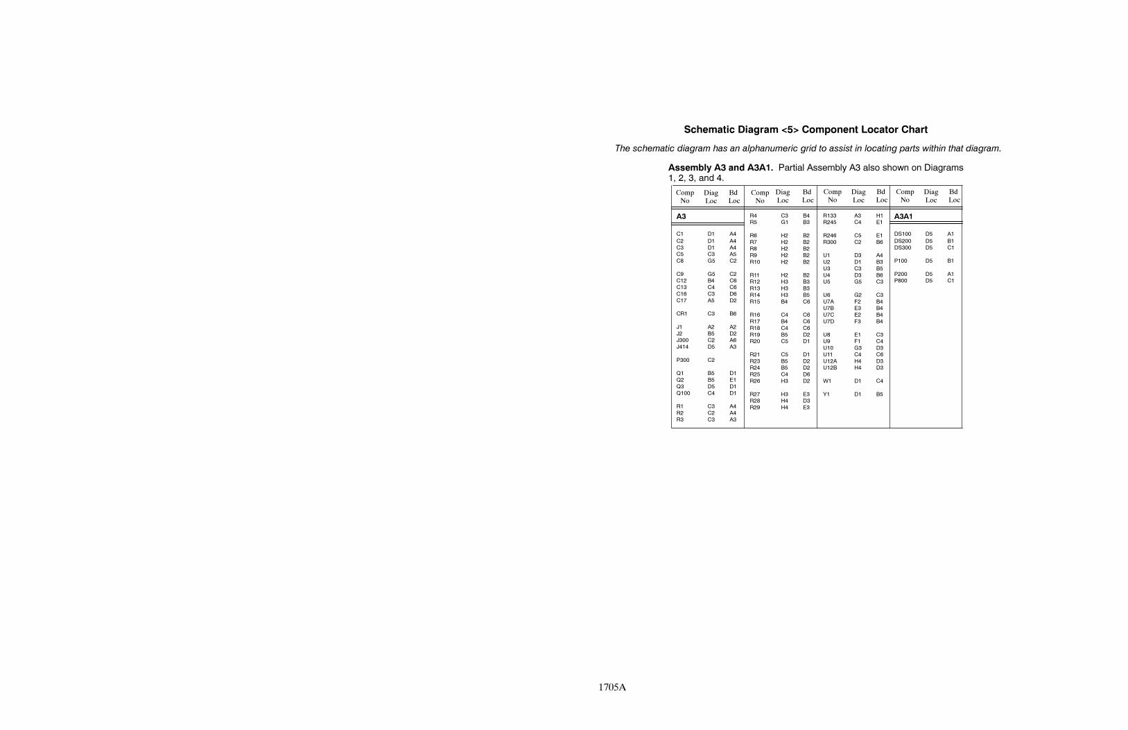
A3
C1 D1 A4
C2 D1 A4
C3 D1 A4
C5 C3 A5
C8 G5 C2
C9 G5 C2
C12 B4 C6
C13 C4 C6
C16 C3 D6
C17 A5 D2
CR1 C3 B6
J1 A2 A2
J2 B5 D2
J300 C2 A6
J414 D5 A3
P300 C2
Q1 B5 D1
Q2 B5 E1
Q3 D5 D1
Q100 C4 D1
R1 C3 A4
R2 C2 A4
R3 C3 A3
R4 C3 B4
R5 G1 B3
R6 H2 B2
R7 H2 B2
R8 H2 B2
R9 H2 B2
R10 H2 B2
R11 H2 B2
R12 H3 B3
R13 H3 B3
R14 H3 B5
R15 B4 C6
R16 C4 C6
R17 B4 C6
R18 C4 C6
R19 B5 D2
R20 C5 D1
R21 C5 D1
R23 B5 D2
R24 B5 D2
R25 C4 D6
R26 H3 D2
R27 H3 E3
R28 H4 D3
R29 H4 E3
R133 A3 H1
R245 C4 E1
R246 C5 E1
R300 C2 B6
U1 D3 A4
U2 D1 B3
U3 C3 B5
U4 D3 B6
U5 G5 C3
U6 G2 C3
U7A F2 B4
U7B E3 B4
U7C E2 B4
U7D F3 B4
U8 E1 C3
U9 F1 C4
U10 G3 D3
U11 C4 C6
U12A H4 D3
U12B H4 D3
W1 D1 C4
Y1 D1 B5
Schematic Diagram <5> Component Locator Chart
CompNo
The schematic diagram has an alphanumeric grid to assist in locating parts within that diagram.
DiagLoc
BdLoc
CompNo
CompNo
DiagLoc
BdLoc
Assembly A3 and A3A1. Partial Assembly A3 also shown on Diagrams1, 2, 3, and 4.
BdLoc
DiagLoc
1705A
CompNo
DiagLoc
BdLoc
A3A1
DS100 D5 A1
DS200 D5 B1
DS300 D5 C1
P100 D5 B1
P200 D5 A1
P800 D5 C1
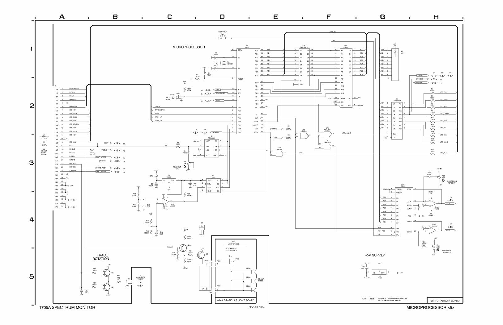
100.0
AD[0..7]
A0
8031 ONLY
W10 OHM
MICROPROCESSOR
Y112MHZ
EA/VP31
X119
X218
RESET9
INT012
INT113
T014
T115
P1.01
P1.12
P1.23
P1.34
P1.45
P1.56
P1.67
P1.78
P0.039
P0.138
P0.237
P0.336
P0.435
P0.534
P0.633
P0.732
P2.021
P2.122
P2.223
P2.324
P2.425
P2.526
P2.627
P2.728
RD17
WR16
PSEN29
ALE/P30
TXD11
RXD10
U28031
R210.0K
C333PF
C233PF
C110UF
+5V
D12
Q119
D23
Q218
D34
Q317
D45
Q416
D56
Q515
D67
Q614
D78
Q713
D89
Q812
C11
OC1
U874ALS573
AD0
AD1
AD2
AD3
AD4
AD5
AD6
AD7
A010
A19
A28
A37
A46
A55
A64
A73
A825
A924
A1021
A1123
A122
O011
O112
O213
O315
O416
O517
O618
O719
PGM27
CE20
OE22
VPP1
NC26
U927C64
AD0
AD1
AD2
AD3
AD4
AD5
AD6
AD7
/VFILTER
/LBAND
/10KHZ
AD0
AD1
AD2
AD3
AD4
AD5
AD6
AD7
+5V
12
3
4
5
6
7
8
9
10
R510K
<2> A4
<1>
B4
<3> <3>
B2 D1
<4> E2
R10100.0
R9100.0
R8100.0
R7100.0
R6100.0
LED_ON
LED_300K
LED_10K
LED_LBAND
LED_70M
D12
Q119
D23
Q218
D34
Q317
D45
Q416
D56
Q515
D67
Q614
D78
Q713
D89
Q812
CLK11
OC1
U674ALS574
AD0
AD1
AD2
AD3
AD4
AD5
AD6
NC+5V
+5V
NC
NC
B4
C1
<3>
<4>
<3>
B2R30010.0K
2DB
RO---BLANK
/1MHZ
+5V
HALFSPAN
12
J300P300
FILTER
INPUT
SPAN_UP
SPAN_DN
BANDWIDTH
NC
FILTER
INPUT
SPAN_UP
SPAN_DN
LED_LBAND
LED_FULL
LED_10M
LED_1M
LED_100K
BANDWIDTH1A
1
1B2
2A3
2B4
3A5
3B6
4A7
4B8
5A9
5B10
6A11
6B12
7A13
7B14
8A15
8B16
9A17
9B18
10A19
10B20
11A21
11B22
12A23
12B24
13A25
13B26
14A27
14B28
15A29
15B30
16A31
16B32
17A33
17B34
J1
CONNECTSTO J303
FRONT
BOARD
<6>
A2
PANEL
J1
H1
NC
<4>
<3>
<3>
<3>
R13368.1K
FOCUS
INTENS
CFT
SWP_SPEED
ROTATE
SCALE
CFT
LED_ON
LED_300K
LED_10K
LED_70M
INTENS
S_SPD
FOCUS
D5
B3
A1
A3
R315.0K
CFT
<4>
E3
<3>
C5
VREF5
+IN2
DO6
--- IN3
VCC8
CLK7
CS1
GND4
U1ADC0831
R17.32K
R42K
/RO---EN
+5V
+5V
<3>
C2
<3>
C3
4
56
U7B74ALS00
9
108
U7C74ALS00
FULL
/10MHZ
/FULL
12
1311
U7D74ALS00
1
23
U7A74ALS00
LED---CONT
AD7
R14100.0
R13
R12100.0
R11100.0
LED_1M
LED_10M
LED_100K
LED_FULL
HORZ POSNREADOUT
<4>
E3
2
31
8
4
U12ATL072
R2720K
R2620.0K
XAXIS
+11.8V
+11.8V
---5V
VREFA4
VREFB18
WR16
CS15
A/B6
D77
D68
D59
D410
D311
D212
D113
D014
RFBA3
OUTA2
AGND1
OUTB20
RFBB19
DGND5
VDD17
U107528
AD0
AD1
AD2
AD3
---5V
R2524.3K
VCC8
RCL6
STO7
GND5
DI3
DO4
CLK2
CE1
U42444
C16.1UF
NC
CALREADOUT
H2
H4
CR1
R154.02K
R174.32K
2
37
6
8
5
1
4U11
LM311
+15V
+5V
C12.1UF
IN3
OUT1
G
2
U378L05
C5100UF
NC
NC<4>
<4>
VERT_POSN
HORZ_POSN
V_POSN
H_POSN
+11.8V
---11.8V
+5V
R16150.0K
R18150.0K
R204.75K
Q100SCALE
+5V
C1310UF B C E
Q3
R2451.00K
+11.8V
J100
LIGHT ENABLE
1---2 ENABLE
R2820.0K
AD4
AD5
AD6
AD7
/WR
/RO---POS
A0
+5V
<4>
E3
5
67
U12BTL072
R2920K
YAXIS
+11.8V
---11.8V
VERT POSNREADOUT
---5V--5V SUPPLY
C8.1UF
IN2
OUT3G
1
U579L05---11.8V
---5V
FRONTPANEL
DS300
DS200
DS100
R21100.0
---11.8V
---15V12
34
J414R2461.00K
Q3
2---3 DISABLE
12
P200
12
P800
1 2 3
P100
CONNECTSTO CRT
<8>
H1
J2
12
J2
ROTATION
TRACE
1/2W
Q1
R23100.0
R24100.0
R19180
Q2
C17.1UF
+15V
---15V
1705A SPECTRUM MONITOR
A3A1 GRATICULE LIGHT BOARD
REV JUL 1994
NOTE:
MICROPROCESSOR <5>
AND SERIAL NUMBER RANGES.SEE PARTS LIST FOR EARLIER VALUES
PART OF A3 MAIN BOARD
A2
DS112 A1
DS112A B1
DS112B A3
DS112C B3
DS129 B1
DS129A B1
DS129B B3
DS129C B1
DS130 B1
DS144 C1
DS144A C1
DS144B B3
DS144C C1
DS145 C1
DS319 A2
DS319A A2
DS319B B3
DS319C B2
DS319D B3
DS319E C2
DS319F B3
DS319G D2
DS325 B2
DS330 B2
DS337 B2
J303 H1 A2
R211 E2 A1
R235 F3 B2
R343 D2 C3
R411 F3 A3
R419 E3 A3
R428 E3 B3
R444 D2 C3
R511 D3 A4
R528 D3 B4
S109 E1 A1
S123 F1 B1
S139 E1 C1
S311 E2 A2
S345 F2 C2
Schematic Diagram <6> Component Locator Chart
CompNo
The schematic diagram has an alphanumeric grid toassist in locating parts within that diagram.
DiagLoc
BdLoc
CompNo
Assembly A2 and A4.
BdLoc
DiagLoc
1705A
A4
C491 D4 B1
C497 D4 C1
C580 C4 A1
C581 C4 A2
C583 B5 A1
C682 A5 A2
C683 B5 A2
C684 B5 B2
C690 E4 B2
C697 F4 C2
C782 A5 A3
CR481 C4 A1
CR485 D4 B1
CR494 D4 C1
CR594 D4 D1
DS698 F5 C2
J698 G4 D2
L591 D4 B1
L695 F4 C2
Q481 C4 A1
Q482 C5 A1
Q588 E5 B2
Q596 D4 D1
Q783 B5 B3
R485 C4 B1
R494 D4 C1
R581 C4 A2
R585 D4 B1
R586 B5 B2
R587 E5 B1
R588 D5 B1
R680 A5 A2
R681 A5 A2
R682 B5 A2
R685 C5 B2
R686 C5 B2
R687 E4 B2
R688 E4 B2
R690 E4 B2
R691 E4 B2
R692 F4 B2
R693 F4 B2
R696 F4 C2
S100 G5
U583 C5 A2
W698 G4
Static Sensitive Devices
See Maintenance Section
A4 18V Power Supply Board
A2 Front Panel Board
FILTERRESOLUTION
FILTERVIDEO
+5V
2
1DS144A
DS144RESOLUTION
+5V
2
1DS129A
DS129VIDEO
+5V
2
1DS112A
DS112FILTER
ON
LED_ON
+5V
FILTER300 KHz
FILTERRESOLUTION
10 KHz
INPUTL BAND
INPUT70 MHz
LED_300K
LED_10K
+5V
+5V
DS130
6
5DS129C
LED_LBAND
LED_70M
+5V
+5V
DS145
6
5DS144C
INPUT
SPAN/DIV+5V
S109
S139
SPAN/DIV
FILTER BANDWIDTH
INPUT
S123
NC
FILTER
INPUT
SPAN_UP
SPAN_DN
LED_LBAND
LED_FULL
LED_10M
LED_1M
LED_100K
BANDWIDTH1A
1
1B2
2A3
2B4
3A5
3B6
4A7
4B8
5A9
5B10
6A11
6B12
7A13
7B14
8A15
8B16
9A17
9B18
10A19
10B20
11A21
11B22
12A23
12B24
13A25
13B26
14A27
14B28
15A29
15B30
16A31
16B32
17A33
17B34
J303
CONNECTS
BOARD
J303
<5>
A3MAIN
TO J1
A2
NC
ROTATE
CFT
INTENS
FOCUS
SCALE
LED_ON
LED_300K
LED_10K
LED_70M
S_SPD
H_POSN
SPAN_UPSPAN_DN
S345
R21120K
LED_FULL
S311DS337SPAN/DIV
FULL
R44420K
LED_10M
R34335.7K
DS330
10
9DS319E
14
13
DS319G
SPAN/DIV1 MHz
SPAN/DIV10 MHz
LED_1M
DS325
6
5DS319C
NOTE: OLD LED PART REFERENCENUMBERS SILKSCREENED ON BOARD,AND IN PARTS LIST.
SPAN/DIV100 KHz
LED_100K
2
1DS319A
DS319
NOT INSTALLED
4
3DS112B
6
5DS112C
4
3DS129B
4
3DS319B
8
7DS319D
4
3DS144B
12
11
DS319F
INTENS
POSITIONVERTICAL R528
20K
INTENS
V_POSN
+11.8V
+11.8V
---11.8V
---11.8V
SCALE
SWEEPSPEED
R42820K
SCALE
S_SPD
+11.8V
+11.8V
---11.8V
FOCUSR41120K
FOCUS
+11.8V
+11.8V
---11.8V
NC
NC
V_POSN
---11.8V
+11.8V
+5V
A2 FRONT PANEL BOARD
GND FROM J23
<4>
10 TURN
CENTERFREQUENCY
R23520K
CFTTRACEROTATION
R41920K
ROTATE
---11.8V
HORIZONTALPOSITION
R51120K
H_POSN
---11.8V
+15V
C581.1UF
R5811.50K
C580100UF
B C E
Q596
CR481
Q481
R485475.0
CR485C4911UF
R49471.5
CR494
Q596
+40V
R585475.0
CR594
R69012W
Q588
R6873.01K
C690100UF
R6881.00K
R6913.01K
L591250UH
C49710UF
R6923.01K
R6933.01K
11
22
33
44
55
J698
+40V
+15V
DS698
L695100UH
R6961K1/2W
C69710UF
NC
ON OFF
+40V
+15V
11
22
33
44
55
W698 FROM J21
FROM J22 A3MAINBOARD
REARPANEL
REARPANEL
LNB POWER
NC
<1>
E5
S100
+18V
LNB POWER
R5881.00K
R5871.00K
Q482
R68656.2K
+3.75V
C5832200PF
VCC1
VZ2
FB3
GAIN4
GND8
OUT7
SEN6
RC5
U583NE5561N
C683.01UF
R68515.0K
R58610.0K
R682267.0K
+8.2V
R68110.0K
Q783
C684.01UF
R6807.50KC782
10UF
C682.1UF
1705A SPECTRUM MONITOR FRONT PANEL & 18V SUPPLY <6>
A4 18V POWER SUPPLY BOARD
A1 Power Supply Board Component Locator (with cross-references to schematic diagrams 7 and 8).
CompNo
DiagNo
DiagLoc
BdLoc
CompNo
DiagNo
DiagLoc
BdLoc
CompNo
DiagNo
DiagLoc
BdLoc
CompNo
DiagNo
DiagLoc
BdLoc
CompNo
DiagNo
DiagLoc
BdLoc
CompNo
DiagNo
DiagLoc
BdLoc
1705A
C1 8 C4 A4
C2 8 D3 D1
C3 8 D3 A2
C4 8 D3 A2
C5 8 D4 B3
C6 8 C4 B4
C7 8 F3 B1
C8 8 D3 B2
C9 8 E2 B2
C10 8 C5 B4
C11 8 E2 B1
C12 8 D2 C4
C13 8 D2 C4
C14 8 D2 C4
C15 8 F2 C4
C16 8 C2 C3
C17 8 F2 D4
C18 8 F3 E1
C19 8 C1 D4
C20 8 C2 D4
C21 8 C1 D4
C22 8 B2 E2
C23 8 B2 E3
C24 8 D1 E4
C25 8 A3 E2
C27 8 B1 E3
C28 8 B1 E3
C29 7 F2 F1
C30 7 F2 F2
C31 7 F3 F3
C32 7 F2 F3
C33 7 G2 F4
C34 8 D1 F4
C35 7 F3 G3
C36 7 G2 G3
C37 7 G3 G4
C38 7 G2 G4
C39 7 E4 G4
C40 7 F4 H4
C41 7 E4 I4
C42 7 D3 I1
C43 7 C4 J4
C44 7 D2 I3
C45 7 D4 I4
C46 7 C5 I4
C47 7 A3 J3
C48 7 C4 J4
C49 7 D3 J2
C50 7 C3 J2
C51 7 C3 K2
C52 7 C4 J2
C53 7 E3 I2
C54 7 C2 M2
C55 7 E3 H3
C56 7 B2 M3
C57 7 B2 N5
C58 7 B3 J2
C59 7 B4 J3
C60 7 B5 J4
C61 7 D4 I4
C62 7 E1 H1
C63 7 E1 G1
C65 8 B2 F4
C66 8 A2 E2
CR1 8 E2 B1
CR2 8 D4 B3
CR3 8 E2 B1
CR4 8 C2 B2
CR5 8 D2 C3
CR6 8 E2 C3
CR7 8 C2 D4
CR8 8 C2 D4
CR9 8 C1 E4
CR10 7 F1 G2
CR11 7 F2 G2
CR12 7 F2 G1
CR13 7 F3 G2
CR14 7 E2 G3
CR15 7 E4 G5
CR16 7 D5 I4
CR17 7 E2 I2
CR18 7 D2 I2
CR19 7 B3 K3
CR20 7 E3 I3
CR21 7 B2 L4
CR22 7 B2 L4
CR23 7 B2 L4
CR24 7 B2 L4
CR25 7 B3 J2
CR26 7 F4 H4
CR27 7 D3 J1
CR28 7 G4 H5
CR29 7 E4 H5
CR30 8 A2 E2
CR31 8 A2 E2
DS1 8 E2 B2
DS2 8 E2 B2
DS3 8 E3 B2
DS4 7 D2 L2
F1 7 B2 M4
FIL1 8 C3 C1
FIL2 8 C3 C1
J1 8 F3 B1
J2 7 H5 B5
J3 8 F2 D1
J4 7 H3 F5
J5 7 H1 F1
J6 7 A2 M3
J10 7 A2 N1
J11 8 F4 A2
L1 7 F3 F2
L2 7 F2 G1
L3 7 F2 G2
L4 7 C2 N1
Q1 8 E5 B3
Q2 8 E5 A3
Q3 8 D4 B4
Q4 8 D4 B4
Q5 8 C4 B4
Q6 8 B2 E1
Q7 7 D5 I4
Q8 7 E4 I4
Q9 7 D3 J1
Q10 8 A2 E2
Q11 7 G3 G3
R1 8 E3 A1
R2 8 E4 A2
R3 8 E4 A2
R4 8 E4 A3
R5 8 E5 A3
R7 8 B4 A4
R8 8 B4 A4
R11 8 F4 A2
R12 8 D3 C1
R13 7 F3 H4
R14 7 G3 H4
R20 8 C4 A4
R21 8 C5 A4
R22 8 D5 A4
R23 8 B4 A4
R24 8 D5 A4
R25 8 B4 A4
R26 8 E5 A3
R27 8 E5 A4
R28 8 E5 A4
R29 8 D2 B1
R30 8 D2 A2
R31 8 D4 B3
R32 8 E5 B3
R33 8 C4 B4
R34 8 C4 B4
R35 8 D4 B3
R36 8 D4 B3
R37 8 C5 B4
R38 8 E2 B1
R39 8 E2 B1
R40 8 D2 B2
R41 8 D4 B3
R42 8 E3 C1
R43 8 E2 B3
R44 8 D2 B3
R45 8 F2 C4
R46 8 E3 C1
R47 8 D2 C3
R48 8 C2 C4
R49 8 F2 C4
R50 8 F2 E1
R51 8 F3 E1
R52 8 F2 E1
R53 8 F2 E1
R54 8 F2 E1
R55 8 D2 D4
R56 8 F3 E1
R57 8 B2 E1
R58 8 D2 E4
R59 8 B1 E2
R60 8 C1 E3
R61 8 D1 E4
R62 7 D4 I4
R63 8 A2 E2
R64 8 C2 E2
R65 8 B1 E3
R66 8 B1 E3
R67 7 F2 F4
R68 7 F4 G5
R69 7 G4 G5
R70 7 G4 G4
R71 7 F4 H4
R72 7 D5 H4
R73 7 E5 I4
R74 7 C4 J5
R75 7 B5 J4
R76 7 C5 I4
R77 7 D4 I4
R78 7 B4 J4
R79 7 B3 J2
R80 7 C4 J4
R81 7 D3 J1
R82 7 C3 J2
R83 7 C5 J2
R84 7 B5 J2
R85 7 G4 H5
R86 7 D3 J1
R87 7 D3 K2
R88 7 B4 J2
R89 7 B2 M4
R90 7 E3 I3
R91 7 D2 K1
R92 7 D2 K1
R93 7 D2 L2
R94 7 D2 L2
R95 7 B4 J3
R96 7 A4 K3
R97 7 A3 J3
R98 7 F4 H4
R99 7 G5 H5
R101 7 C3 K2
R102 7 C2 M1
R103 8 A2 E2
RV1 7 D2 I3
T1 8 B2 C4
T2 7 E4 H5
T3 7 E2 G3
TP1 7 F5 F4
TP2 7 E5 K4
U1 8 D1 C1
U2 8 B1 F4
U3A 7 C4 J3
U3B 7 B3 J3
U4A 7 D4 I5
U4B 7 C4 I5
U5 7 C3 J2
VR1 7 F4 H4
VR2 8 A2 E2
VR3 7 F3 H4
VR4 7 F4 H4
W1 7 G3 E4
W2 7 G3 E4
W3 7 G2 E4
W4 7 G2 E5
CompNo
DiagNo
DiagLoc
BdLoc
CompNo
DiagNo
DiagLoc
BdLoc
CompNo
DiagNo
DiagLoc
BdLoc
CompNo
DiagNo
DiagLoc
BdLoc
CompNo
DiagNo
DiagLoc
BdLoc
Static Sensitive Devices
See Maintenance Section
A1 Power Supply Board
* SEE PARTS LIST FOR EFFECTIVE SERIAL NUMBER RANGES
11
22
33
44
55
66
77
88
99
1010
1111
J5
CAUTION: ALL CIRCUITRY TO THE
MOUNTING
LINE RECTIFIERAND FILTER
L41MH
LEFT OF THE ISOLATIONBOUNDARY IS AT POWER LINEPOTENTIAL AND REQUIRESAN ISOLATION TRANSFORMERTO SERVICE
BOUNDARYISOLATION
CLAMP
C63NOT INSTALLED
C62NOT INSTALLED
OUTPUT FILTERSL3
4.7UH
CR10
1700F10
(DC OPER.)
UPGRADEONLY
USED WITH
C36560UF
C38560UF
W30 OHM
W40 OHM
+15A
+15V
+40V
---15A
---15V
C30560UF
C29560UF
L24.7UH
R6710.0
CR12
CR11
RV1NOT INSTALLED
CR18NOT INSTALLED
10
8
14
13
12
11
9
2
1
5
6
7
T3
CR14
C44.47UF
R93150K
R94150K
R91100K
R92100K
R1028
DS4
C54330UFCR23 CR22
CR21CR24
90---250V
C56.022UF
F12A
C57.068UF
R895
J10REARPANEL
J6
OUTPUT UVSHUTDOWN
5
67
U3BLM393
R972.00K
+5VC
C47.47UF
CR19
CR25
PULSEWIDTH
MODULATOR
COMP1
VFB2
ISEN3
RT/CT4
REF 8
VCC7
OUT 6
GND5
U5UC3842
+5VC
SWITCHERMOSFET
C49.1UF
C42560UF
C50.47UF
CR27
SNUBBER
C53100PF
C55NOT INSTALLED
CR17 C32560UF
L14.7UH
C31560UF
C35560UF
+5V
CR13
W10 OHM
W20 OHM
+40VA
+5D
+5V
C3310UF
C37560UF
NCJ4
CONNECTSTO J4
A3MAIN
BOARD
+100V
+5V
+15V
+40V<4>
11
22
33
44
55
66
77
88
99
1010
J4
ZAXIS
FOCUS
J4---1A4
A4
D5
<8>
<8>
<8>
+5V
Q11
ERROR
R13100
R1410.05.1V
VR3
H
BOUNDARYISOLATION
Q9
R86.51
R902.4K CR20
Q9
R8722.1
R824.99K
R81178
R10149.9
NC
NCR882.00K
+5VC
R7949.9K
C58200PF
C51.01UF
CL
11
CX6
RX7
B10
A9
Q 12
Q 5
U4B74HC221A
C59.1UF
R9649.9K
R754.99K
+5VC
R783.74K
R954.53K
3
21
8
4
U3ALM393
R744.99K
C43.47UF
C52.01UF
+5VC +5VC
FEEDBACKTRANSFORMER
DRIVER
NC
NC
NC
C45.47UF
C48200PF
R802.00K
+5VC
+5VC
+5VCCL
3
VCC16
GND 8
CX14
RX15
B2
A1
Q4
Q13
U4A74HC221A
R77100
G D S
AMPLIFIER
C41.47UF
C39.1UF
+5VC
C61470PF
CR151
2
4
3
T2
Q8
CR29
R62100
C404700PF
R9810.00K
+40V
10V
CR26
VR1
VR4
R68178
R71221K
+5V
R6910.00K
R7010.00K
R99100K
+5V
+5V ADJUST
R85100K
POWER
FRONTPANEL
(OPEN = ON)
---15V
S1
12
12
J2
TP1
LINE SIDE COMMONSECONDARY GROUND(CHASSIS GROUND)
R7210.0
R7310.0
TP2
+5VC
+5VC
CR16
Q7
C46.01UF
PEAKDETECTOR
R8310.00K
+5VC
R763.74K
R8418.7K
C60.1UF
1705A SPECTRUM MONITOR LOW VOLTS POWER SUPPLY <7>
AND SERIAL NUMBER RANGES.SEE PARTS LIST FOR EARLIER VALUESNOTE:
PART OF A1 POWER SUPPLY
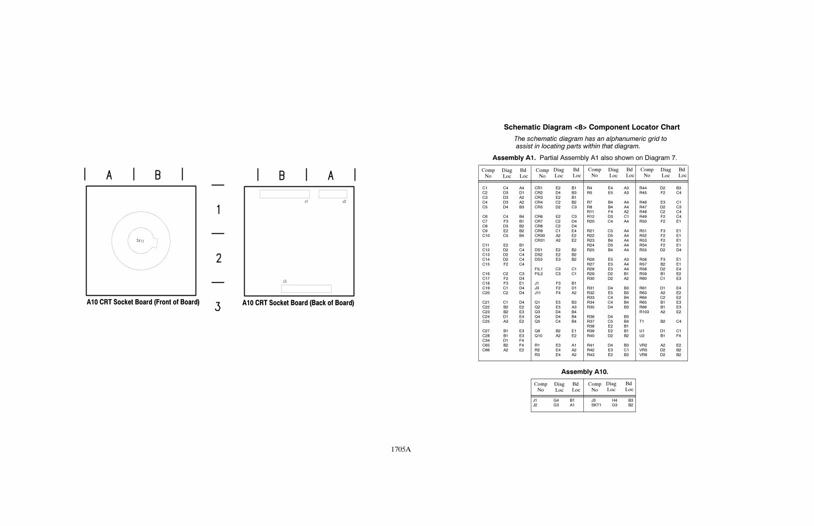
C1 C4 A4
C2 D3 D1
C3 D3 A2
C4 D3 A2
C5 D4 B3
C6 C4 B4
C7 F3 B1
C8 D3 B2
C9 E2 B2
C10 C5 B4
C11 E2 B1
C12 D2 C4
C13 D2 C4
C14 D2 C4
C15 F2 C4
C16 C2 C3
C17 F2 D4
C18 F3 E1
C19 C1 D4
C20 C2 D4
C21 C1 D4
C22 B2 E2
C23 B2 E3
C24 D1 E4
C25 A3 E2
C27 B1 E3
C28 B1 E3
C34 D1 F4
C65 B2 F4
C66 A2 E2
CR1 E2 B1
CR2 D4 B3
CR3 E2 B1
CR4 C2 B2
CR5 D2 C3
CR6 E2 C3
CR7 C2 D4
CR8 C2 D4
CR9 C1 E4
CR30 A2 E2
CR31 A2 E2
DS1 E2 B2
DS2 E2 B2
DS3 E3 B2
FIL1 C3 C1
FIL2 C3 C1
J1 F3 B1
J3 F2 D1
J11 F4 A2
Q1 E5 B3
Q2 E5 A3
Q3 D4 B4
Q4 D4 B4
Q5 C4 B4
Q6 B2 E1
Q10 A2 E2
R1 E3 A1
R2 E4 A2
R3 E4 A2
R4 E4 A3
R5 E5 A3
R7 B4 A4
R8 B4 A4
R11 F4 A2
R12 D3 C1
R20 C4 A4
R21 C5 A4
R22 D5 A4
R23 B4 A4
R24 D5 A4
R25 B4 A4
R26 E5 A3
R27 E5 A4
R28 E5 A4
R29 D2 B1
R30 D2 A2
R31 D4 B3
R32 E5 B3
R33 C4 B4
R34 C4 B4
R35 D4 B3
R36 D4 B3
R37 C5 B4
R38 E2 B1
R39 E2 B1
R40 D2 B2
R41 D4 B3
R42 E3 C1
R43 E2 B3
R44 D2 B3
R45 F2 C4
R46 E3 C1
R47 D2 C3
R48 C2 C4
R49 F2 C4
R50 F2 E1
R51 F3 E1
R52 F2 E1
R53 F2 E1
R54 F2 E1
R55 D2 D4
R56 F3 E1
R57 B2 E1
R58 D2 E4
R59 B1 E2
R60 C1 E3
R61 D1 E4
R63 A2 E2
R64 C2 E2
R65 B1 E3
R66 B1 E3
R103 A2 E2
T1 B2 C4
U1 D1 C1
U2 B1 F4
VR2 A2 E2
VR5 D2 B2
VR6 D2 B2
1705A
CompNo
DiagLoc
BdLoc
CompNo
CompNo
DiagLoc
BdLoc
CompNo
DiagLoc
BdLoc
BdLoc
DiagLoc
Schematic Diagram <8> Component Locator Chart
The schematic diagram has an alphanumeric grid toassist in locating parts within that diagram.
Assembly A1. Partial Assembly A1 also shown on Diagram 7.
A10 CRT Socket Board (Front of Board) A10 CRT Socket Board (Back of Board)
CompNo
DiagLoc
BdLoc
CompNo
BdLoc
DiagLoc
Assembly A10.
J1 G4 B1
J2 G3 A1
J3 H4 B3
SKT1 G3 B2
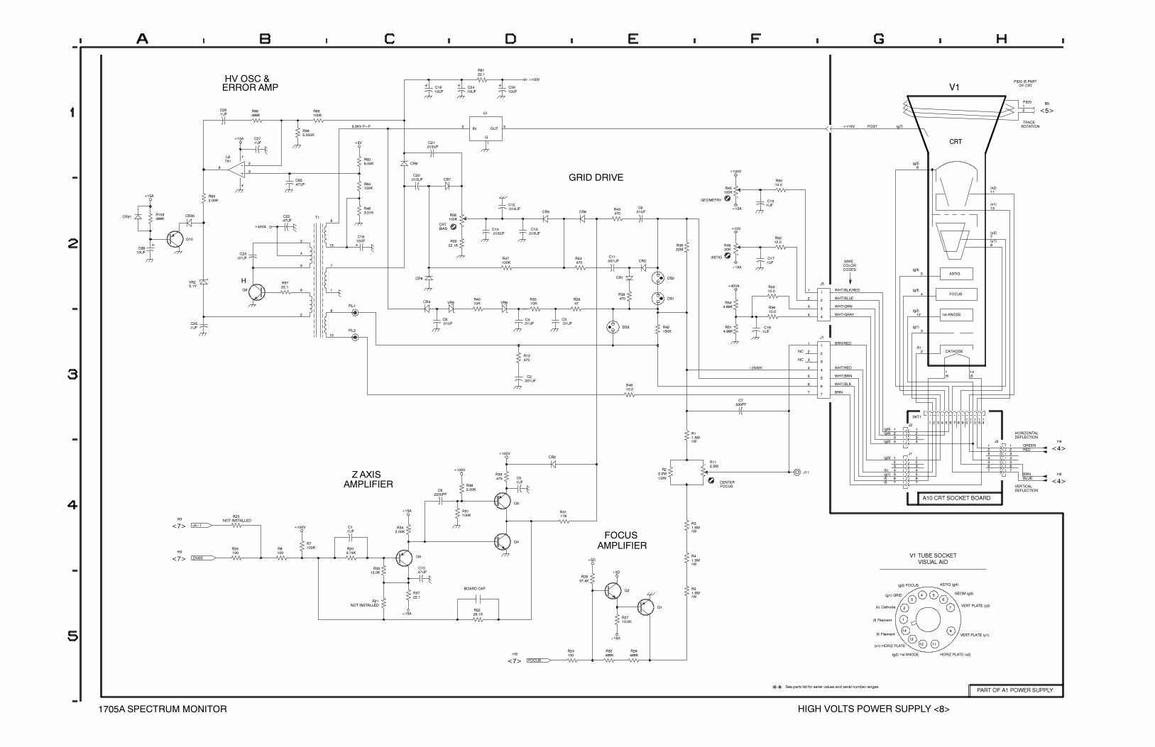
20K
P320 IS PARTOF CRT
V1
R6122.1
+100V
C1910UF
C2410UF
C3410UF
HV OSC &ERROR AMP
C27.1UF
2
36
7
4
U2741
R66499K
+15A
C28.1UF
R632.00K
5.5KV P---P
R65100K
R64100K
C20.015UF
+5V
R606.04K
R595.000K
CR9
C65.47UF
C21.015UF
CR7
IN2
OUT3
G
1
U1
GRID DRIVER45100K
R5010.0
+100V
POST+11KV
CRT
6(g5)
(g7)
P320
ROTATIONTRACE
12
(x2)
<5>
B5
9
7
13
11
(x1)
(y2)
(y1)
COLORCODES
WIRE
ASTIG5(g4)
GEOMETRY
ASTIG
C15.1UF
C17.1UF
R5210.0
---15A
---15A
11
22
33
44
J3
R49
+15V
R3822M
R44470
R43470
R39470
C11.001UF
C9.01UF
DS2CR1
CR3
CR6
CRTBIAS
R58100K
C12.015UF
C14.015UF
C13.015UF
R47100K
R5522.1K
CR8
CR5C22.47UF
R5722.1
R483.01K
C1610UF5
4
3
6
2
8
13
7
1
9
10
T1
H5.1V
C23.01UF
+40VA
C6610UF
+15A
R103499K
Q6
VR2
Q10
CR30CR31
C25.1UF
FIL2
FIL1
R12470
C2.001UF
C3.01UF
C4.01UF
C8.01UF
R4010K
R3010KCR4 VR6VR5
R42150K
R2947
DS3
DS1
---2530V
NC
NC
R5310.0
R5610.0
R544.99K
R514.99K
C18.1UF
+40VA
11
22
33
44
55
66
77
J1
WHT/BLUE
WHT/GRAY
BRN/RED
WHT/RED
WHT/BRN
WHT/BLK/RED
WHT/GRN
1st ANODE
FOCUS
14
3
2 CATHODE
4
1
(g3)
12(g2)
(g1)
(k)
(f) (f)
H4
H2
1234567
GREENRED
BRNBLUE
HORIZONTALDEFLECTION
J31234567
<4>
WHT/BLK
BRN
1234
1234567
(f)(g1)(k)
(g3)
(g2)
(g4)(g5) 1
234
J1
J2
1234567
1 2 3 4 5 6 7 8 910
11
12
13
14
SKT1
R112.5M
C7330PF
J11
1W
1/2W
R4610.0
R11.5M
R22.2M
R362.00K
R35475
+100V
+100VCR2
Z AXIS
R8100
R25100
R23NOT INSTALLED
ZAXIS
J4---1<7>
H3
H3
<7>
AMPLIFIER
R342.00K
R3313.0K
C1.1UF
+100V
+15A
R203.74K
R7100K
Q5
R31100K
C5.1UF
C62200PF
C10.47UF
Q4
Q3
FOCUSAMPLIFIER
1W
1W
R2837.4K
R31.5M
R41.5M
R41178
+5D
CENTERFOCUS
V1 TUBE SOCKET
VISUAL AID
(f)
A10 CRT SOCKET BOARD
<4>
DEFLECTIONVERTICAL
14
13
12 11
9
7
654
3
2
1
ASTIG (g4)
GEOM (g5)
VERT PLATE (y2)
VERT PLATE (y1)
(g2) 1st ANODE
(x1) HORIZ PLATE
(f) Filament
(f) Filament
(k) Cathode
(g1) GRID
(g3) FOCUS
HORIZ PLATE (x2)
1W
R24100
R2713.0K
R32499K
R26499K
R51.5M
+5D
---15A
Q2
Q1
BOARD CAP
FOCUS
H3
<7>
R2226.1K
R3722.1
R21NOT INSTALLED
---15A
1705A SPECTRUM MONITOR HIGH VOLTS POWER SUPPLY <8>
See parts list for earier values and serial number ranges.PART OF A1 POWER SUPPLY


Replaceable Mechanical Parts


1705A Spectrum Monitor 10--1
Section 10Replaceable Mechanical Parts
This section contains a list of the components that are replaceable for the 1705A.Use this list to identify and order replacement parts. There is a separateReplaceable Mechanical Parts list for each instrument.
Parts Ordering InformationReplacement parts are available from or through your local Tektronix, Inc., FieldOffice or representative.
Changes to Tektronix instruments are sometimes made to accommodateimproved components as they become available and to give you the benefit ofthe latest circuit improvements. Therefore, when ordering parts, it is important toinclude the following information in your order.
Part number Instrument type or model number Instrument serial number Instrument modification number, if applicable
If a part you have ordered has been replaced with a new or improved part, yourlocal Tektronix, Inc., Field Office or representative will contact you concerningany change in part number.
Change information, if any, is located at the rear of this manual.
Using the Replaceable Mechanical Parts ListThe tabular information in the Replaceable Mechanical Parts list is arranged forquick retrieval. Understanding the structure and features of the list will help youfind all of the information you need for ordering replaceable parts.
The Mfg. Code Number to Manufacturer Cross Index for the mechanical partslist is located immediately after this page. The cross index provides codes,names, and addresses of manufacturers of components listed in the mechanicalparts list.
Abbreviations conform to American National Standards Institute (ANSI)standard Y1.1.
Chassis-mounted parts and cable assemblies are located at the end of theReplaceable Electrical Parts list.
Cross Index-Mfr. CodeNumber to Manufacturer
Abbreviations
Chassis Parts
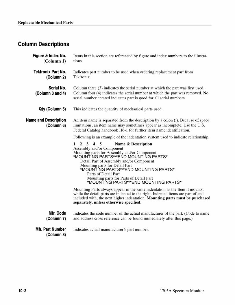
Replaceable Mechanical Parts
10- 2 1705A Spectrum Monitor
Column Descriptions
Items in this section are referenced by figure and index numbers to the illustra-tions.
Indicates part number to be used when ordering replacement part fromTektronix.
Column three (3) indicates the serial number at which the part was first used.Column four (4) indicates the serial number at which the part was removed. Noserial number entered indicates part is good for all serial numbers.
This indicates the quantity of mechanical parts used.
An item name is separated from the description by a colon (:). Because of spacelimitations, an item name may sometimes appear as incomplete. Use the U.S.Federal Catalog handbook H6-1 for further item name identification.
Following is an example of the indentation system used to indicate relationship.
1 2 3 4 5 Name & DescriptionAssembly and/or ComponentMounting parts for Assembly and/or Component*MOUNTING PARTS*/*END MOUNTING PARTS*
Detail Part of Assembly and/or ComponentMounting parts for Detail Part*MOUNTING PARTS*/*END MOUNTING PARTS*
Parts of Detail PartMounting parts for Parts of Detail Part*MOUNTING PARTS*/*END MOUNTING PARTS*
Mounting Parts always appear in the same indentation as the Item it mounts,while the detail parts are indented to the right. Indented items are part of andincluded with, the next higher indentation. Mounting parts must be purchasedseparately, unless otherwise specified.
Indicates the code number of the actual manufacturer of the part. (Code to nameand address cross reference can be found immediately after this page.)
Indicates actual manufacturer’s part number.
Figure & Index No.(Column 1)
Tektronix Part No.(Column 2)
Serial No.(Column 3 and 4)
Qty (Column 5)
Name and Description(Column 6)
Mfr. Code(Column 7)
Mfr. Part Number(Column 8)
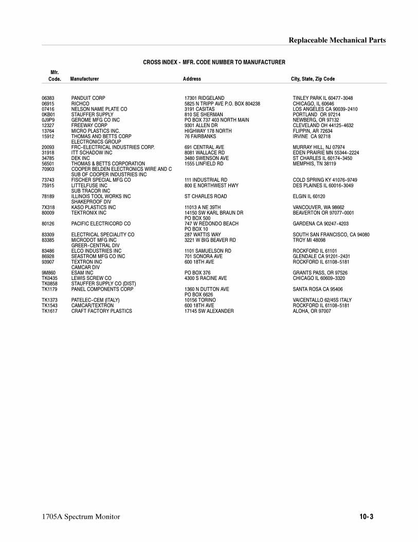
Replaceable Mechanical Parts
1705A Spectrum Monitor 10- 3
CROSS INDEX - MFR. CODE NUMBER TO MANUFACTURER
Mfr.
Code. Manufacturer Address City, State, Zip Code
06383 PANDUIT CORP 17301 RIDGELAND TINLEY PARK IL 60477--304806915 RICHCO 5825 N TRIPP AVE P.O. BOX 804238 CHICAGO, IL 6064607416 NELSON NAME PLATE CO 3191 CASITAS LOS ANGELES CA 90039--24100KB01 STAUFFER SUPPLY 810 SE SHERMAN PORTLAND OR 972140J9P9 GEROME MFG CO INC PO BOX 737 403 NORTH MAIN NEWBERG, OR 9713212327 FREEWAY CORP 9301 ALLEN DR CLEVELAND OH 44125--463213764 MICRO PLASTICS INC. HIGHWAY 178 NORTH FLIPPIN, AR 7263415912 THOMAS AND BETTS CORP 76 FAIRBANKS IRVINE CA 92718
ELECTRONICS GROUP20093 FRC--ELECTRICAL INDUSTRIES CORP. 691 CENTRAL AVE MURRAY HILL, NJ 0797431918 ITT SCHADOW INC 8081 WALLACE RD EDEN PRAIRIE MN 55344--222434785 DEK INC 3480 SWENSON AVE ST CHARLES IL 60174--345056501 THOMAS & BETTS CORPORATION 1555 LINFIELD RD MEMPHIS, TN 3811970903 COOPER BELDEN ELECTRONICS WIRE AND C
SUB OF COOPER INDUSTRIES INC73743 FISCHER SPECIAL MFG CO 111 INDUSTRIAL RD COLD SPRING KY 41076--974975915 LITTELFUSE INC 800 E NORTHWEST HWY DES PLAINES IL 60016--3049
SUB TRACOR INC78189 ILLINOIS TOOL WORKS INC ST CHARLES ROAD ELGIN IL 60120
SHAKEPROOF DIV7X318 KASO PLASTICS INC 11013 A NE 39TH VANCOUVER, WA 9866280009 TEKTRONIX INC 14150 SW KARL BRAUN DR BEAVERTON OR 97077--0001
PO BOX 50080126 PACIFIC ELECTRICORD CO 747 W REDONDO BEACH GARDENA CA 90247--4203
PO BOX 1083309 ELECTRICAL SPECIALITY CO 287 WATTIS WAY SOUTH SAN FRANCISCO, CA 9408083385 MICRODOT MFG INC 3221 W BIG BEAVER RD TROY MI 48098
GREER--CENTRAL DIV83486 ELCO INDUSTRIES INC 1101 SAMUELSON RD ROCKFORD IL 6110186928 SEASTROM MFG CO INC 701 SONORA AVE GLENDALE CA 91201--243193907 TEXTRON INC 600 18TH AVE ROCKFORD IL 61108--5181
CAMCAR DIV9M860 ESAM INC PO BOX 376 GRANTS PASS, OR 97526TK0435 LEWIS SCREW CO 4300 S RACINE AVE CHICAGO IL 60609--3320TK0858 STAUFFER SUPPLY CO (DIST)TK1179 PANEL COMPONENTS CORP 1360 N DUTTON AVE SANTA ROSA CA 95406
PO BOX 6626TK1373 PATELEC--CEM (ITALY) 10156 TORINO VAICENTALLO 62/45S ITALYTK1543 CAMCAR/TEXTRON 600 18TH AVE ROCKFORD IL 61108--5181TK1617 CRAFT FACTORY PLASTICS 17145 SW ALEXANDER ALOHA, OR 97007
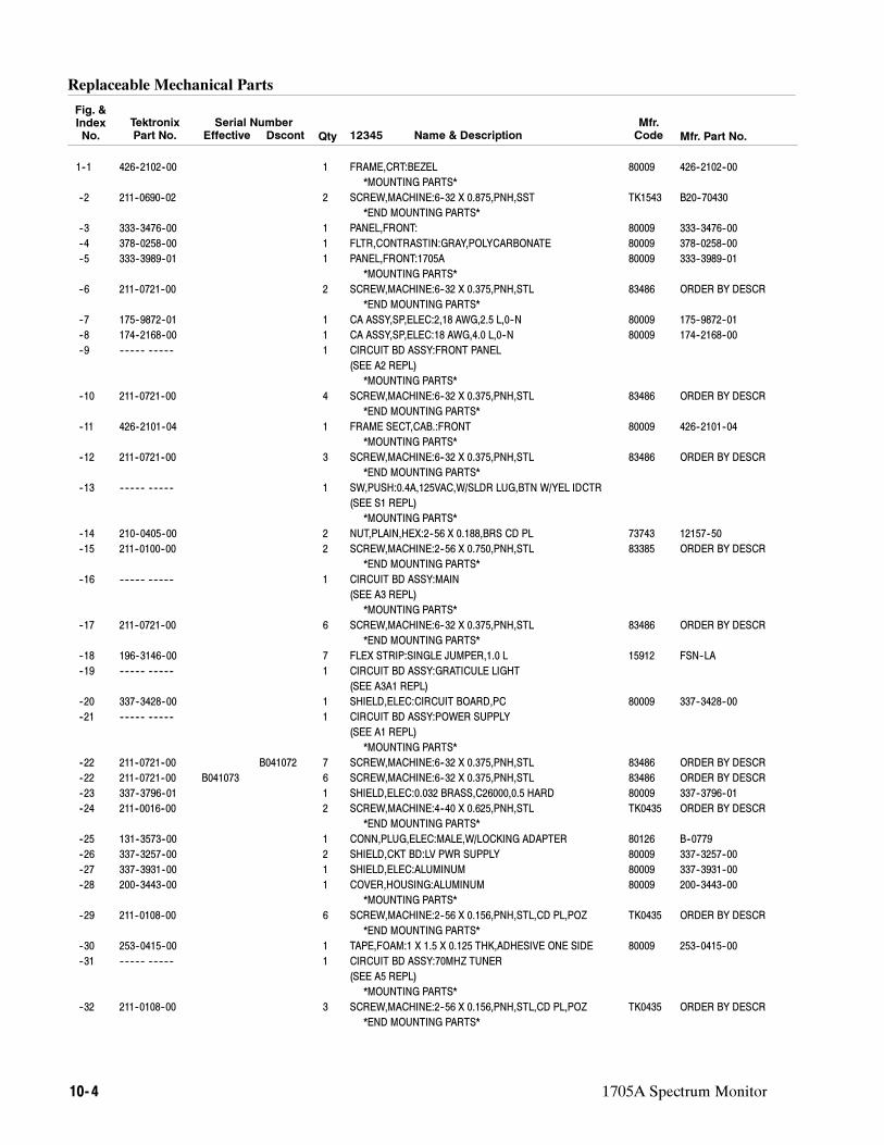
Replaceable Mechanical Parts
10- 4 1705A Spectrum Monitor
Fig. &IndexNo.
TektronixPart No.
Serial NumberEffective Dscont Qty 12345 Name & Description
Mfr.Code Mfr. Part No.
1--1 426--2102--00 1 FRAME,CRT:BEZEL 80009 426--2102--00
*MOUNTING PARTS*
--2 211--0690--02 2 SCREW,MACHINE:6--32 X 0.875,PNH,SST TK1543 B20--70430
*END MOUNTING PARTS*
--3 333--3476--00 1 PANEL,FRONT: 80009 333--3476--00
--4 378--0258--00 1 FLTR,CONTRASTIN:GRAY,POLYCARBONATE 80009 378--0258--00
--5 333--3989--01 1 PANEL,FRONT:1705A 80009 333--3989--01
*MOUNTING PARTS*
--6 211--0721--00 2 SCREW,MACHINE:6--32 X 0.375,PNH,STL 83486 ORDER BY DESCR
*END MOUNTING PARTS*
--7 175--9872--01 1 CA ASSY,SP,ELEC:2,18 AWG,2.5 L,0--N 80009 175--9872--01
--8 174--2168--00 1 CA ASSY,SP,ELEC:18 AWG,4.0 L,0--N 80009 174--2168--00
--9 -- -- -- -- -- -- -- -- -- -- 1 CIRCUIT BD ASSY:FRONT PANEL
(SEE A2 REPL)
*MOUNTING PARTS*
--10 211--0721--00 4 SCREW,MACHINE:6--32 X 0.375,PNH,STL 83486 ORDER BY DESCR
*END MOUNTING PARTS*
--11 426--2101--04 1 FRAME SECT,CAB.:FRONT 80009 426--2101--04
*MOUNTING PARTS*
--12 211--0721--00 3 SCREW,MACHINE:6--32 X 0.375,PNH,STL 83486 ORDER BY DESCR
*END MOUNTING PARTS*
--13 -- -- -- -- -- -- -- -- -- -- 1 SW,PUSH:0.4A,125VAC,W/SLDR LUG,BTN W/YEL IDCTR
(SEE S1 REPL)
*MOUNTING PARTS*
--14 210--0405--00 2 NUT,PLAIN,HEX:2--56 X 0.188,BRS CD PL 73743 12157--50
--15 211--0100--00 2 SCREW,MACHINE:2--56 X 0.750,PNH,STL 83385 ORDER BY DESCR
*END MOUNTING PARTS*
--16 -- -- -- -- -- -- -- -- -- -- 1 CIRCUIT BD ASSY:MAIN
(SEE A3 REPL)
*MOUNTING PARTS*
--17 211--0721--00 6 SCREW,MACHINE:6--32 X 0.375,PNH,STL 83486 ORDER BY DESCR
*END MOUNTING PARTS*
--18 196--3146--00 7 FLEX STRIP:SINGLE JUMPER,1.0 L 15912 FSN--LA
--19 -- -- -- -- -- -- -- -- -- -- 1 CIRCUIT BD ASSY:GRATICULE LIGHT
(SEE A3A1 REPL)
--20 337--3428--00 1 SHIELD,ELEC:CIRCUIT BOARD,PC 80009 337--3428--00
--21 -- -- -- -- -- -- -- -- -- -- 1 CIRCUIT BD ASSY:POWER SUPPLY
(SEE A1 REPL)
*MOUNTING PARTS*
--22 211--0721--00 B041072 7 SCREW,MACHINE:6--32 X 0.375,PNH,STL 83486 ORDER BY DESCR
--22 211--0721--00 B041073 6 SCREW,MACHINE:6--32 X 0.375,PNH,STL 83486 ORDER BY DESCR
--23 337--3796--01 1 SHIELD,ELEC:0.032 BRASS,C26000,0.5 HARD 80009 337--3796--01
--24 211--0016--00 2 SCREW,MACHINE:4--40 X 0.625,PNH,STL TK0435 ORDER BY DESCR
*END MOUNTING PARTS*
--25 131--3573--00 1 CONN,PLUG,ELEC:MALE,W/LOCKING ADAPTER 80126 B--0779
--26 337--3257--00 2 SHIELD,CKT BD:LV PWR SUPPLY 80009 337--3257--00
--27 337--3931--00 1 SHIELD,ELEC:ALUMINUM 80009 337--3931--00
--28 200--3443--00 1 COVER,HOUSING:ALUMINUM 80009 200--3443--00
*MOUNTING PARTS*
--29 211--0108--00 6 SCREW,MACHINE:2--56 X 0.156,PNH,STL,CD PL,POZ TK0435 ORDER BY DESCR
*END MOUNTING PARTS*
--30 253--0415--00 1 TAPE,FOAM:1 X 1.5 X 0.125 THK,ADHESIVE ONE SIDE 80009 253--0415--00
--31 -- -- -- -- -- -- -- -- -- -- 1 CIRCUIT BD ASSY:70MHZ TUNER
(SEE A5 REPL)
*MOUNTING PARTS*
--32 211--0108--00 3 SCREW,MACHINE:2--56 X 0.156,PNH,STL,CD PL,POZ TK0435 ORDER BY DESCR
*END MOUNTING PARTS*
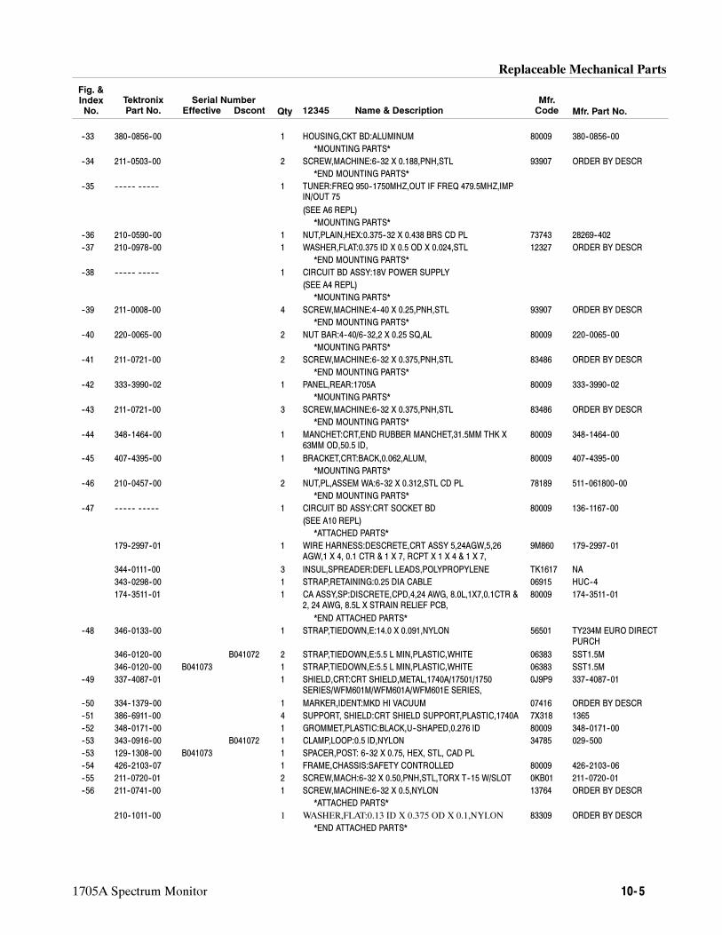
Replaceable Mechanical Parts
1705A Spectrum Monitor 10- 5
Fig. &IndexNo. Mfr. Part No.
Mfr.Code12345 Name & DescriptionQty
Serial NumberEffective Dscont
TektronixPart No.
--33 380--0856--00 1 HOUSING,CKT BD:ALUMINUM 80009 380--0856--00
*MOUNTING PARTS*
--34 211--0503--00 2 SCREW,MACHINE:6--32 X 0.188,PNH,STL 93907 ORDER BY DESCR
*END MOUNTING PARTS*
--35 -- -- -- -- -- -- -- -- -- -- 1 TUNER:FREQ 950--1750MHZ,OUT IF FREQ 479.5MHZ,IMPIN/OUT 75
(SEE A6 REPL)
*MOUNTING PARTS*
--36 210--0590--00 1 NUT,PLAIN,HEX:0.375--32 X 0.438 BRS CD PL 73743 28269--402
--37 210--0978--00 1 WASHER,FLAT:0.375 ID X 0.5 OD X 0.024,STL 12327 ORDER BY DESCR
*END MOUNTING PARTS*
--38 -- -- -- -- -- -- -- -- -- -- 1 CIRCUIT BD ASSY:18V POWER SUPPLY
(SEE A4 REPL)
*MOUNTING PARTS*
--39 211--0008--00 4 SCREW,MACHINE:4--40 X 0.25,PNH,STL 93907 ORDER BY DESCR
*END MOUNTING PARTS*
--40 220--0065--00 2 NUT BAR:4--40/6--32,2 X 0.25 SQ,AL 80009 220--0065--00
*MOUNTING PARTS*
--41 211--0721--00 2 SCREW,MACHINE:6--32 X 0.375,PNH,STL 83486 ORDER BY DESCR
*END MOUNTING PARTS*
--42 333--3990--02 1 PANEL,REAR:1705A 80009 333--3990--02
*MOUNTING PARTS*
--43 211--0721--00 3 SCREW,MACHINE:6--32 X 0.375,PNH,STL 83486 ORDER BY DESCR
*END MOUNTING PARTS*
--44 348--1464--00 1 MANCHET:CRT,END RUBBER MANCHET,31.5MM THK X63MM OD,50.5 ID,
80009 348--1464--00
--45 407--4395--00 1 BRACKET,CRT:BACK,0.062,ALUM, 80009 407--4395--00
*MOUNTING PARTS*
--46 210--0457--00 2 NUT,PL,ASSEM WA:6--32 X 0.312,STL CD PL 78189 511--061800--00
*END MOUNTING PARTS*
--47 -- -- -- -- -- -- -- -- -- -- 1 CIRCUIT BD ASSY:CRT SOCKET BD 80009 136--1167--00
(SEE A10 REPL)
*ATTACHED PARTS*
179--2997--01 1 WIRE HARNESS:DESCRETE,CRT ASSY 5,24AGW,5,26AGW,1 X 4, 0.1 CTR & 1 X 7, RCPT X 1 X 4 & 1 X 7,
9M860 179--2997--01
344--0111--00 3 INSUL,SPREADER:DEFL LEADS,POLYPROPYLENE TK1617 NA
343--0298--00 1 STRAP,RETAINING:0.25 DIA CABLE 06915 HUC--4
174--3511--01 1 CA ASSY,SP:DISCRETE,CPD,4,24 AWG, 8.0L,1X7,0.1CTR &2, 24 AWG, 8.5L X STRAIN RELIEF PCB,
80009 174--3511--01
*END ATTACHED PARTS*
--48 346--0133--00 1 STRAP,TIEDOWN,E:14.0 X 0.091,NYLON 56501 TY234M EURO DIRECTPURCH
346--0120--00 B041072 2 STRAP,TIEDOWN,E:5.5 L MIN,PLASTIC,WHITE 06383 SST1.5M
346--0120--00 B041073 1 STRAP,TIEDOWN,E:5.5 L MIN,PLASTIC,WHITE 06383 SST1.5M
--49 337--4087--01 1 SHIELD,CRT:CRT SHIELD,METAL,1740A/17501/1750SERIES/WFM601M/WFM601A/WFM601E SERIES,
0J9P9 337--4087--01
--50 334--1379--00 1 MARKER,IDENT:MKD HI VACUUM 07416 ORDER BY DESCR
--51 386--6911--00 4 SUPPORT, SHIELD:CRT SHIELD SUPPORT,PLASTIC,1740A 7X318 1365
--52 348--0171--00 1 GROMMET,PLASTIC:BLACK,U--SHAPED,0.276 ID 80009 348--0171--00
--53 343--0916--00 B041072 1 CLAMP,LOOP:0.5 ID,NYLON 34785 029--500
--53 129--1308--00 B041073 1 SPACER,POST: 6--32 X 0.75, HEX, STL, CAD PL
--54 426--2103--07 1 FRAME,CHASSIS:SAFETY CONTROLLED 80009 426--2103--06
--55 211--0720--01 2 SCREW,MACH:6--32 X 0.50,PNH,STL,TORX T--15 W/SLOT 0KB01 211--0720--01
--56 211--0741--00 1 SCREW,MACHINE:6--32 X 0.5,NYLON 13764 ORDER BY DESCR
*ATTACHED PARTS*
210--1011--00 1 WASHER,FLAT:0.13 ID X 0.375 OD X 0.1,NYLON 83309 ORDER BY DESCR
*END ATTACHED PARTS*
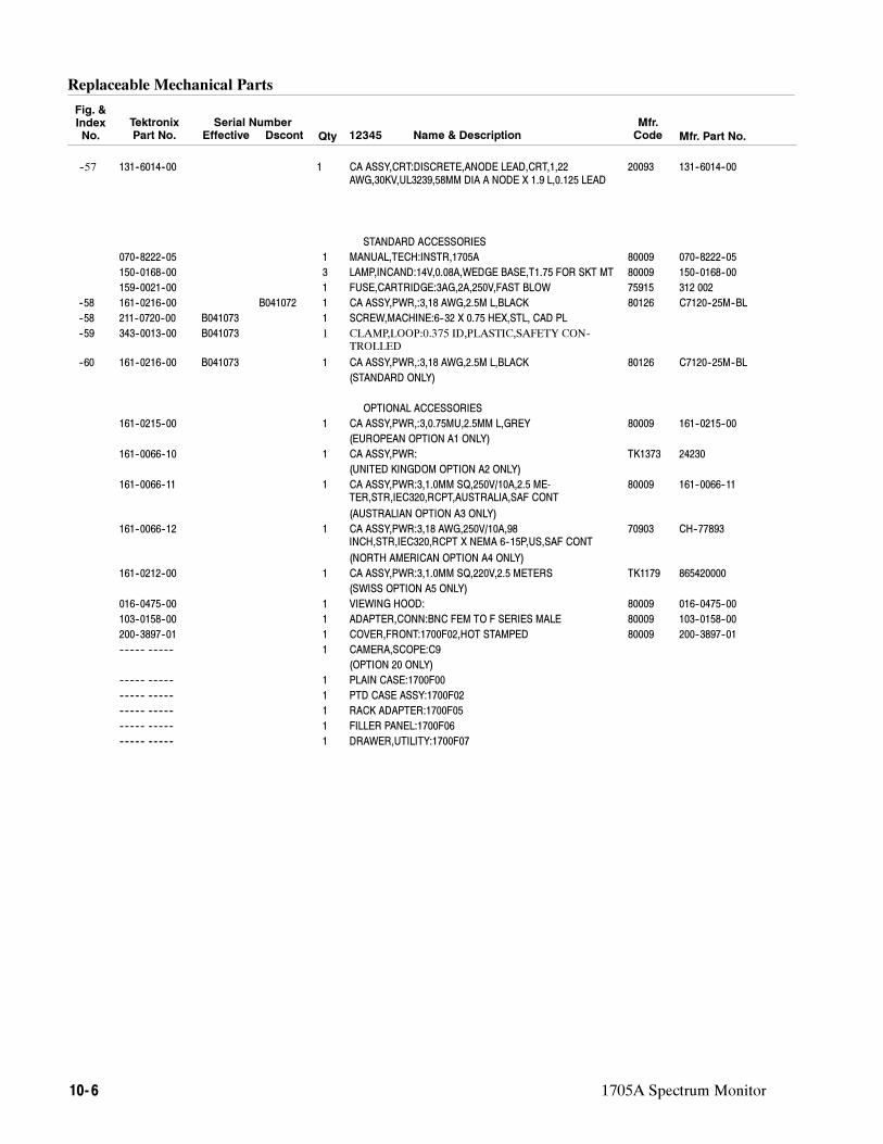
Replaceable Mechanical Parts
10- 6 1705A Spectrum Monitor
Fig. &IndexNo. Mfr. Part No.
Mfr.Code12345 Name & DescriptionQty
Serial NumberEffective Dscont
TektronixPart No.
--57 131--6014--00 1 CA ASSY,CRT:DISCRETE,ANODE LEAD,CRT,1,22AWG,30KV,UL3239,58MM DIA A NODE X 1.9 L,0.125 LEAD
20093 131--6014--00
STANDARD ACCESSORIES
070--8222--05 1 MANUAL,TECH:INSTR,1705A 80009 070--8222--05
150--0168--00 3 LAMP,INCAND:14V,0.08A,WEDGE BASE,T1.75 FOR SKT MT 80009 150--0168--00
159--0021--00 1 FUSE,CARTRIDGE:3AG,2A,250V,FAST BLOW 75915 312 002
--58 161--0216--00 B041072 1 CA ASSY,PWR,:3,18 AWG,2.5M L,BLACK 80126 C7120--25M--BL
--58 211--0720--00 B041073 1 SCREW,MACHINE:6--32 X 0.75 HEX,STL, CAD PL
--59 343--0013--00 B041073 1 CLAMP,LOOP:0.375 ID,PLASTIC,SAFETY CON-TROLLED
--60 161--0216--00 B041073 1 CA ASSY,PWR,:3,18 AWG,2.5M L,BLACK 80126 C7120--25M--BL
(STANDARD ONLY)
OPTIONAL ACCESSORIES
161--0215--00 1 CA ASSY,PWR,:3,0.75MU,2.5MM L,GREY 80009 161--0215--00
(EUROPEAN OPTION A1 ONLY)
161--0066--10 1 CA ASSY,PWR: TK1373 24230
(UNITED KINGDOM OPTION A2 ONLY)
161--0066--11 1 CA ASSY,PWR:3,1.0MM SQ,250V/10A,2.5 ME-TER,STR,IEC320,RCPT,AUSTRALIA,SAF CONT
80009 161--0066--11
(AUSTRALIAN OPTION A3 ONLY)
161--0066--12 1 CA ASSY,PWR:3,18 AWG,250V/10A,98INCH,STR,IEC320,RCPT X NEMA 6--15P,US,SAF CONT
70903 CH--77893
(NORTH AMERICAN OPTION A4 ONLY)
161--0212--00 1 CA ASSY,PWR:3,1.0MM SQ,220V,2.5 METERS TK1179 865420000
(SWISS OPTION A5 ONLY)
016--0475--00 1 VIEWING HOOD: 80009 016--0475--00
103--0158--00 1 ADAPTER,CONN:BNC FEM TO F SERIES MALE 80009 103--0158--00
200--3897--01 1 COVER,FRONT:1700F02,HOT STAMPED 80009 200--3897--01
-- -- -- -- -- -- -- -- -- -- 1 CAMERA,SCOPE:C9
(OPTION 20 ONLY)
-- -- -- -- -- -- -- -- -- -- 1 PLAIN CASE:1700F00
-- -- -- -- -- -- -- -- -- -- 1 PTD CASE ASSY:1700F02
-- -- -- -- -- -- -- -- -- -- 1 RACK ADAPTER:1700F05
-- -- -- -- -- -- -- -- -- -- 1 FILLER PANEL:1700F06
-- -- -- -- -- -- -- -- -- -- 1 DRAWER,UTILITY:1700F07
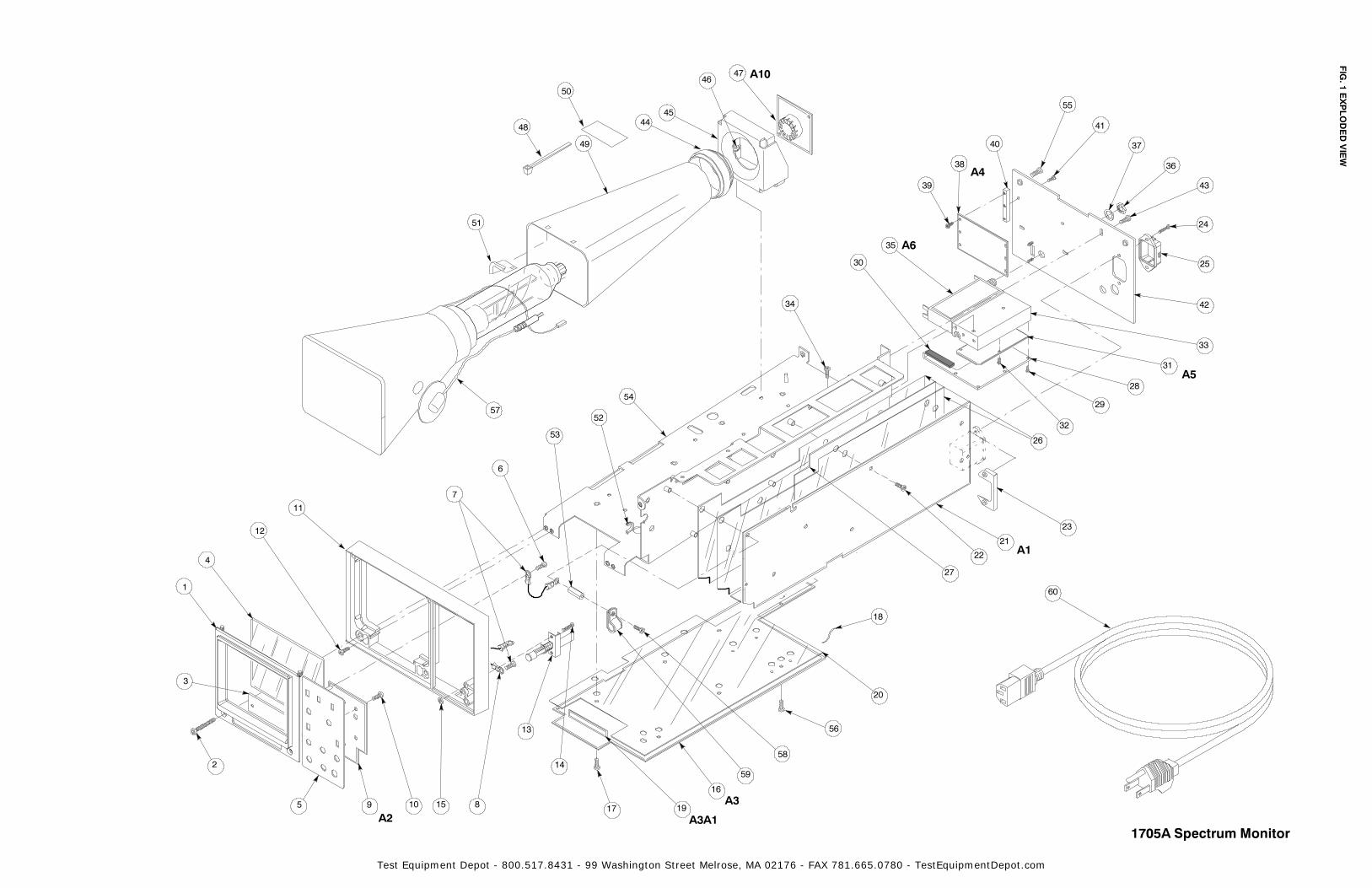
1705A Spectrum Monitor
FIG
.1EXPLODED
VIEW
A1
A3
A2 A3A1
1
2
3
4
5
6
7
89 10
11
12
13
14
15
16
17
18
19
20
21
22
23
24
25
26
27
28
29
30
31
A5
32
33
34
35 A6
A436
37
38
39
40
41
42
43
44
45
4647
48
49
50
51
52
53
54
55
57
A10
56
58
59
60
Test Equipment Depot - 800.517.8431 - 99 Washington Street Melrose, MA 02176 - FAX 781.665.0780 - TestEquipmentDepot.com