Embed Size (px)
Citation preview
1632 IEEE SENSORS JOURNAL, VOL. 7, NO. 12, DECEMBER 2007
Fabrication of SiO2 Microcantilever UsingIsotropic Etching With ICP
Qi Chen, Ji Fang, Hai-Feng Ji, and Kody Varahramyan
Abstract—This paper reports a new design and microfabricationprocess for high sensing guard-armed silicon dioxide (SiO2) mi-crocantilever sensor, which can be widely used in chemical, envi-ronmental and biomedical applications. One sensor platform con-sists of two SiO2 cantilever beams as the sensing and reference el-ements, two connecting wings, and three guard arms. The guardarms prevent damage to the cantilever beam from collision. Toefficiently release the SiO2 cantilevers from the silicon substrate,an isotropic etch method using inductively coupled plasma (ICP)was developed. The isotropic etching with ICP system providesan advantage in good profile control and high etching rate thanwet isotropic etching or conventional RIE (reactive ion etching);however, it has not been gained many attentions. In this work,the effects of chamber pressure, plasma source power, substratepower, SF6 flow rate relating with Si etching rate, undercuttingrate, and isotropic ratio were investigated and discussed. The op-timum isotropic etching process achieved a 9.1 m/min etch rate,70% isotropic ratio, and 92% etching uniformity. The SiO2 can-tilever sensor was fabricated and the cantilever beam was success-fully released using a patterned photoresist layer as an etchingmask. This plasma isotropic etching release processing can be alsoapplied to release other SiO2 or metal suspended MEMS struc-tures, such as bridges and membranes, with a fast etch rate andreasonable isotropic ratio.
Index Terms—Isotropic etching with inductively coupled plasma(ICP) and cantilever design, silicon dioxide (SiO2) cantilever.
I. INTRODUCTION
MICROCANTILEVERS have recently attracted consider-able interests in the development of physical, chemical,
and biological sensors [1]–[9]. Microcantilever can undergobending due to molecular adsorption or absorption by confiningthe adsorption and absorption to one side of the cantileverwhere the sensing material is coated. Adsorption or interactionof the analyte will change the surface characteristics of themicrocantilever or the film volume on the cantilever, and resultin the bending of the microcantilever. This concept has alreadybeen used to demonstrate the feasibility of chemical detectionof a number of vapor phase analytes, as well as highly sensitivedetection of chemical and biological species in solutions. Mostof these microcantilever sensors were made of silicon. Due
Manuscript received January 26, 2007; revised April 15, 2007; accepted April30, 2007. This work was supported in part by the National Science FoundationSensor and Sensor Network under ECS-0428263 and in part by the Board ofRegent Industrial Ties and Research Subprogram under Contract LEQSF(2005-04)-RD-B-19. The associate editor coordinating the review of this paper andapproving it for publication was Prof. Michael Pishko.
The authors are with the Institute for Micromanufacturing, Louisiana TechUniversity, Ruston, LA 71270 USA (e-mail: [email protected]; [email protected]; [email protected]; [email protected]).
Color versions of one or more of the figures in this paper are available onlineat http://ieeexplore.ieee.org.
Digital Object Identifier 10.1109/JSEN.2007.908922
to the relatively large Young’s modulus of silicon material(169 GPa), the bending response of the silicon microcantileveris too weak to be measured when surface stress change is rathersmall. In the previous works [10], we developed SiO cantileversensor for better sensitivity [10]–[13] by taking advantage ofthe smaller Young’s modulus of SiO (76.5–97.2 GPa) incomparison with silicon or silicon nitride microcantilever.We used a plasma anisotropic dry etching process to releasethe SiO microcantilever beams. To completely release thecantilever beam, the anisotropic dry etching must go throughthe 500- m-thick sacrificial silicon from the backside of wafer.Common photoresist can not be used as an etching mask. Theetching mask material must be carefully selected.
In this work, we developed a SiO cantilever sensor fabri-cation process with a very high etching rate by using isotropicdry etching to completely release the cantilever beam fromboth sides of substrate. For a better understanding the isotropicetching, the effects of reaction chamber pressure, inductivelycoupled plasma (ICP) source power, substrate power, andflow rate on the etch rate, undercut rate, and isotropic ratio havebeen investigated.
II. EXPERIMENTS FOR INVESTIGATING ISOTROPIC
ETCH PROPERTIES
A. Isotropic Plasma Etching
Dry etching with ICP has been extensively studied for the fab-rication of high aspect ratio micromechanical structures. Amongthe available process schemes and recipes, the Bosch process[14], [15] has made high aspect ratio silicon structures with ver-tical sidewalls possible [16]. The standard Bosch process is ananisotropic etching procedure and works as follows. It startswith a shallow etching step under a low pressure SF plasmagenerated with an RF source, fluorine radicals generated in SFplasma then react with silicon to form volatile SiF , and con-tinues with a passivation step enhanced via an ICP source, whereC F gas molecules are dissociated to form a polymeric layerover the exposed silicon surface. During the subsequent etchstep, this layer is preferentially withdrawn on the horizontalsurface rather than on the sidewalls because of ionic physicaletching. Both steps repeat until complete etching of the siliconlayer is accomplished. Experiments and optimization settingsfor anisotropic plasma etching with ICP system have been re-ported [17], [18].
It was recently found that the isotropic etching capability ofICP has certain advantages over anisotropic etching, includinggood controllability [19], high silicon etching rate, and highSiO :Si etching selectivity [10], etc. The silicon isotropicetching procedure is modified from the standard Bosch process[14], [15]. In this modified process, the passivation step was
1530-437X/$25.00 © 2007 IEEE
CHEN et al.: FABRICATION OF SIO MICROCANTILEVER USING ISOTROPIC ETCHING WITH ICP 1633
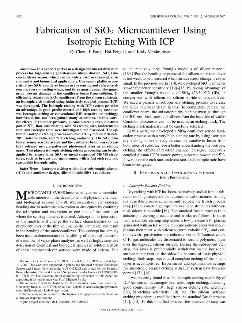
Fig. 1. Pattern of the PR (photoresist) as a mask for cantilever beam release.
dismissed and SF was the only process gas. Since no pas-sivation layer was formed along the sidewall of the trench,the ions reacted freely with the silicon atoms under the maskhorizontally. The isotropic etching was realized largely byion-enhanced chemical etching after was dismissed inthe etching process.
B. Experimental Setup and Procedure
A high-density plasma ICP system (Alcatel 601E) wasused to conduct the experiment. The plasma was generatedby a 13.56 MHz RF power supply and diffused down to alow pressure chamber where the wafer was processed. Theion energy was independently controlled from ion flux by aradio frequency (RF) power applied to the chuck. The waferwas mechanically clamped on the chuck, which was thermallyregulated with liquid nitrogen and a heating element. Thetemperature could be adjusted from C to 50 C. Ahelium pressure-controlled film between the chuck and thewafer ensured better heat transfer. A load chamber optimizedthe load/unload operations without breaking vacuum in theprocess chamber.
The starting material was a commercially available [SiliconInc.] double side polished four-inch (100-mm), siliconwafer with 500 m thick, and a 1- m-thick SiO layer on bothsurfaces. To achieve the structure of microcantilever describedpreviously, four masks were designed and applied. Amongthese, mask 2 was specifically designed for cantilever beamrelease by isotropic plasma dry etching combined with ananisotropic etching process in Fig. 1. Here, Fig. 1(b) depicts anenlarged part of the mask pattern in Fig. 1(a) and the relateddimension of mask 1 and mask 2. The photoresist pattern ofmask 2 served as an etching mask in the ICP etching process torelease the microcantilever beam from bulk silicon. In order toprotect the edges of the cantilever beam, the photoresist patterncovering on the cantilever beam was about 5 m longer alongthe three edges than the SiO beam. This also compensated forany slightly alignment errors. To ensure the cantilever beamreleased completely and the foot of the beam remained at theexpected position after release, the photoresist pattern at thefoot of beam was designed at 60 m longer than mask 1.
The experimental processes for investigating the isotropicetch to release the SiO microcantilever beam is shown inFig. 2. First, after baking for 30 min at 250 C, the wafer wasspin-coated with a 1- m-thick layer of Shipley 1813 positivetone photoresist. Then, the photoresist was patterned by thelithography process using mask 1 (Fig. 2(a)). Next, the SiOcantilever beams were formed by wet etching with bufferedoxidation etchant ( in volume). Then,
Fig. 2. The process for investigation of isotropic plasma etching. (a) Patternresist. (b) Etch SiO . (c) Pattern resist for cantilever beam release. (d) Isotropicetching for 10 min.
the photoresist was removed from the surface of the wafer[Fig. 2(b)]. A 3 m-thick layer of photoresist 1813 was spunonto the wafer and patterned with mask 2 [Fig. 2(c)]. Finally,the isotropic etching processing was applied by the ICP systemto release the cantilever [Fig. 2(d)].
For the best cantilever beam release results, the isotropicetching process was compared using 16 distinct recipes. Eachprocess was initiated with an oxygen cleaning process toremove impurities in the chamber, which would influence theisotropic etching. This cleaning step was applied on a dummywafer for 10 min. The chamber preconditioning process wasfollowed by the designated recipe within 10 min. After thisstep, a processing substrate was loaded into the system forisotropic etching. Pure SF is the only process gas used in thesilicon isotropic etching. A 10-min etching time was conductedin all testing processes in these experiments in order to com-pare the process parameters for isotropic etching. The processparameters varied in the following range: chamber pressure(14–66 mTorr), ICP source power (800–1800 W), substratepower (0–30 W), and SF flow rate (150–300 sccm).
The profiles of released cantilevers were observed by scan-ning electron microscopy (SEM). The resulting SEM pictureswere analyzed using Matlab software. The etching depths weremeasured by a KLA Tencor profilometer (TENCOR Alpha step500 profiler; TENCOR Inc.) with a precision of m.Table I lists the detail of the processing recipes tested and thebest result obtained, as shown in Fig. 3.
C. Results and Discussion
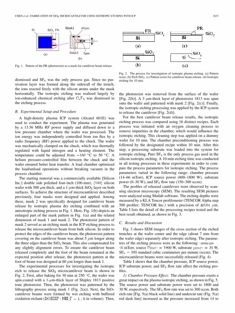
Fig. 3 shows SEM images of the cross section of the etchedtrenches at the wafer center and the edge (about 7 mm fromthe wafer edge) separately after isotropic etching. The parame-ters of the etching process were as the following:
mTorr, source W, substrate W,SF standard cubic centimeters per minute (sccm). Themicrocantilever beams were successfully released (Fig. 4).
Table I shows that the chamber pressure, ICP source power,ICP substrate power, and SF flow rate affect the etching pro-files.
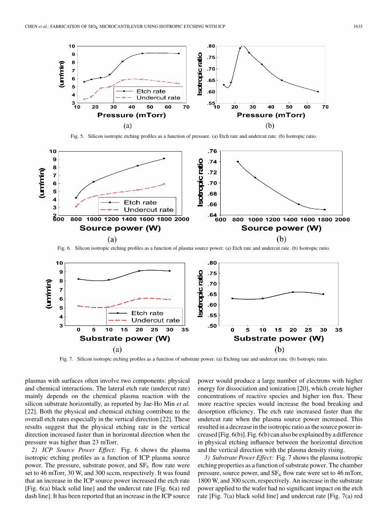
1) Chamber Pressure Effect: The chamber pressure exerts agreat impact on the plasma isotropic etching, as shown in Fig. 5.The source power and substrate power were set to 1800 and30 W, respectively. The SF flow rate was set to 300 sccm. Bothetch rate [Fig. 5(a) black solid line) and undercut rate (Fig. 5(a)red dash line] increased as the pressure increased from 14 to

1634 IEEE SENSORS JOURNAL, VOL. 7, NO. 12, DECEMBER 2007
Fig. 3. SEM images of the cross section of etched trenches. The mask opening was 200 �m in width, and the etching time was 600 s. (a) A trench near the centerof wafer. (b) A trench at the edge of wafer.
TABLE IPROCESS PARAMETERS AND ETCHING PROFILES
Fig. 4. SEM image of the released cantilever beams.
46 mTorr. When the pressure higher than 46 mTorr, the etchrate was the same but undercut rate slightly dropped. Under thepressure range from 14 to 46, the increases in etch rate and un-dercut rate were due to the higher plasma density (especially the
higher number of fluorine radicals) in the chemical reaction athigher pressure [20], [21]. When the pressure was higher than46 mTorr, the chemical reaction tended to saturate and higherpressure would increase the collision frequency, which resultedin the reduction of ion energy [20].
The isotropic ratio in Table I was defined as
where is the horizontal dimension extent of the foot edge fromthe mask edge or the undercut rate, and is the vertical etcheddepth or the etch rate.
The ratio of undercut rate over etch rate gave an isotropicratio, as shown in Fig. 5(b). The highest isotropic ratio appearsat 23 mTorr. In the 14–23 mTorr range, the isotropic ratioincreased when the pressure increased, indicating the enhancedchemical reaction rate which exerted more impact on undercutrate than on etch rate. Above 23 mTorr, the isotropic ratiodecreased as the pressure increased, suggesting differencesbetween undercut and etch rates. Interactions of reactive
CHEN et al.: FABRICATION OF SIO MICROCANTILEVER USING ISOTROPIC ETCHING WITH ICP 1635
Fig. 5. Silicon isotropic etching profiles as a function of pressure. (a) Etch rate and undercut rate. (b) Isotropic ratio.
Fig. 6. Silicon isotropic etching profiles as a function of plasma source power. (a) Etch rate and undercut rate. (b) Isotropic ratio.
Fig. 7. Silicon isotropic etching profiles as a function of substrate power. (a) Etching rate and undercut rate. (b) Isotropic ratio.
plasmas with surfaces often involve two components: physicaland chemical interactions. The lateral etch rate (undercut rate)mainly depends on the chemical plasma reaction with thesilicon substrate horizontally, as reported by Jae-Ho Min et al.[22]. Both the physical and chemical etching contribute to theoverall etch rates especially in the vertical direction [22]. Theseresults suggest that the physical etching rate in the verticaldirection increased faster than in horizontal direction when thepressure was higher than 23 mTorr.
2) ICP Source Power Effect: Fig. 6 shows the plasmaisotropic etching profiles as a function of ICP plasma sourcepower. The pressure, substrate power, and SF flow rate wereset to 46 mTorr, 30 W, and 300 sccm, respectively. It was foundthat an increase in the ICP source power increased the etch rate[Fig. 6(a) black solid line] and the undercut rate [Fig. 6(a) reddash line]. It has been reported that an increase in the ICP source
power would produce a large number of electrons with higherenergy for dissociation and ionization [20], which create higherconcentrations of reactive species and higher ion flux. Thesemore reactive species would increase the bond breaking anddesorption efficiency. The etch rate increased faster than theundercut rate when the plasma source power increased. Thisresulted in a decrease in the isotropic ratio as the source power in-creased [Fig. 6(b)]. Fig. 6(b) can also be explained by a differencein physical etching influence between the horizontal directionand the vertical direction with the plasma density rising.
3) Substrate Power Effect: Fig. 7 shows the plasma isotropicetching properties as a function of substrate power. The chamberpressure, source power, and SF flow rate were set to 46 mTorr,1800 W, and 300 sccm, respectively. An increase in the substratepower applied to the wafer had no significant impact on the etchrate [Fig. 7(a) black solid line] and undercut rate [Fig. 7(a) red
1636 IEEE SENSORS JOURNAL, VOL. 7, NO. 12, DECEMBER 2007
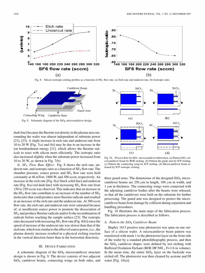
Fig. 8. Silicon isotropic etching profiles as a function of SF flow rate. (a) Etch rate and undercut rate. (b) Isotropic ratio.
Fig. 9. Schematic diagram of the SiO microcantilever design.
dash line] because the fluorine ion density in the plasma area sur-rounding the wafer was almost independent of substrate power[21], [23]. A slight increase in etch rate and undercut rate from10 to 20 W [Fig. 7(a) and (b)] may be due to an increase in theion bombardment energy [21], which allows the fluorine rad-icals to react with silicon more efficiently. The isotropic ratioalso increased slightly when the substrate power increased from10 to 20 W, as shown in Fig. 7(b).
4) SF Flow Rate Effect: Fig. 8 shows the etch rate, un-dercut rate, and isotropic ratio as a function of SF flow rate. Thechamber pressure, source power, and SF flow rate were heldconstantly at 46 mTorr, 1800 W, and 300 sccm, respectively. Anincrease in the etch rate [Fig. 8(a) black solid line] and undercutrate [Fig. 8(a) red dash line] with increasing SF flow rate from150 to 250 sccm was observed. This indicates that an increase inthe SF flow rate contribute to an increase of the number of SFmolecules that could produce more fluorine radicals and resultedin an increase of the etch rate and the undercut rate. At 300 sccmflow rate, the etch rate and undercut rate were saturated becauseof: a) insufficient source power to promote the dissociation ofSF and produce fluorine radicals and/or b) the recombination ofradicals before reaching the sample surface [23]. The isotropicratio decreased with increasing SF flow rate [Fig. 8(b)] since thespeed of increase of the undercut rate was slower than that of theetch rate, which was similar to the effect of source power, (i.e., theplasma density increase resulted in a physical etching reactionin the vertical direction faster than in the horizontal direction).
III. DEVICE FABRICATION
A schematic diagram of the SiO microcantilever structuredesign is shown in Fig. 9. The device consists of two adjacentSiO cantilever beams, connecting wings on both sides, and
Fig. 10. Process flow for SiO microcantilever fabrication. (a) Pattern SiO mi-crocantilever beam by BOE etching. (b) Pattern the guide arm by ICP etching.(c) Pattern the connecting wing by ICP etching. (d) Microcantilever beam re-leased by ICP isotropic etching.
three guard arms. The dimensions of the designed SiO micro-cantilever beams are 250 m in length, 100 m in width, and1 m in thickness. The connecting wings were connected withthe adjoining cantilever bodies after the beams were released,so that all the cantilevers were held on the substrate for furtherprocessing. The guard arm was designed to protect the micro-cantilever beam from damage by collision during separation andhandling procedures.
Fig. 10 illustrates the main steps of the fabrication process.The fabrication process is described as follows.
A. Pattern the SiO Cantilever Beam
Shipley 1813 positive tone photoresist was spun on one sur-face of a silicon wafer. A microcantilever beam pattern wastransferred with mask 1 to the photoresist layer on the front sideof the wafer by a standard photolithography process, and thenthe SiO cantilever shapes were defined by wet etching withBuffered Oxidation Etchant (BOE HF:NH F=1:6 in volume).In the mean time, the entire SiO layer on the backside wasetched off. The photoresist was then cleaned by acetone and DIwater [Fig. 10(a)].

CHEN et al.: FABRICATION OF SIO MICROCANTILEVER USING ISOTROPIC ETCHING WITH ICP 1637
B. Wafer Backside Etching 1: Pattern Cantilever Base WithGuard Arm
A 3- m-thick 1813 photoresist layer was spun on the back-side of the wafer, and then patterned with a photolithographyprocess to form the base of the cantilever sensor. The photore-sist pattern served as a mask for ICP plasma etching to create theguard arm in the next fabrication step. The wafer was etched byabout 70 m by the ICP anisotropic etching process [Fig. 10(b)].The etching depth of about 70 m determined the thickness ofthe connecting arm. This etched area will be completely openedthrough the wafer after releasing the cantilever beam.
C. Wafer Backside Etching 2: Pattern Cantilever ConnectingWing and Guard Arm
A 3 m layer of photoresist 1813 was spun on the backsideof the wafer again and then plasma anisotropic etching appliedto etch about 260 m. This etching step is also applied to etchthe connecting wings, guard arms, and open window from thebackside of the substrate [Fig. 10(c)].
D. Cantilever Beam Release
A new process, which involves two steps was developed torelease the SiO cantilever beam. The cantilever beam wasfirst patterned by anisotropic dry etching and followed by theisotropic plasma dry etching to completely release the can-tilever beam. In the first step, anisotropic etching was appliedto open a window and to ensure the fluorine radicals can reactefficiently with the silicon underneath the SiO beam duringthe isotropic plasma etching. Then, the isotropic plasma etchingwas applied to release the SiO beam from the bulk siliconsubstrate.
A 3 m thick film of photoresist 1813 was spun on the frontside of the wafer, and then the front side of the wafer waspatterned with mask 2 (Fig. 1). The photoresist pattern servedas an etching mask for ICP etching process to release the mi-crocantilever beam from the bulk silicon. The cantilever beamwas released by two plasma dry etching steps: 90- m-thickanisotropic etching, and then isotropic etching until all micro-cantilever beams were released [Fig. 10(d)]. The processingtime for releasing the cantilever was 20 min. The optimal recipefor isotropic etching in this step was chosen by the followinginvestigation and discussions.
The etch rate, undercut rate, and isotropic ratio have beentaken into consideration to obtain an optimal set of plasmaetching parameters. In fact, for the isotropic etch, we hope toachieve higher etch rate, as well as better isotropic ratio at thesame time. Therefore, recipe 13 in Table I (46 mTorr pressure,1800 W source power, substrate power 20 W, 300 sccm SFflow rate, and 20 C chuck temperature) was adopted as the bestone. For this recipe, the etching rate was about 9.1 m/min,uniformity was 92% and isotropic ratio was 66%.
Using this process, the cantilever beam was successfully re-leased from the substrate. Fig. 11 shows the SEM pictures ofone cantilever. The configuration of the several devices is shownin Fig. 12. The connecting wing between two adjacent micro-cantilever bodies should be about 50–70 m thick, so that thethickness is not only sufficient to connect them together, but also
Fig. 11. SEM image of rectangular cantilever beam.
Fig. 12. SEM image of SiO microcantilevers.
easily broken just by applying a little force. The cantilevers canbe easily coated with a sensing polymer or films for differentchemical or biological sensing applications.
Another advantage of this process is that it is easy for us tohandle the problem associated with the photoresist mask, whichoccurred in our previous experiment. During an anisotropic dryetching go through an entire wafer with ICP, the photoresistmask was damaged or etched off because the ions bombard thesurface of the photoresist. The fabrication process we developedwas to divide the release process into three dry etching steps.Meanwhile, the release time is greatly reduced at the higherisotropic etching rate (9.1 m/min). Therefore, the 3- m-thickphotoresist 1813 can be an appropriate mask layer for releasingthe cantilever beam.
IV. CONCLUSION
New SiO microcantilever sensors were designed and fabri-cated using the isotropic dry etching process herein developed.The release of SiO microcantilever beams and the effects ofplasma etching properties on etching rates and undercut rateswere investigated and discussed. The results showed that theplasma density played a major role in the isotropic etchingresults; higher plasma density would result in a higher etchrate and higher undercut rate. The higher plasma density couldbe achieved by increasing pressure, source power or SF flowrate. One optimal recipe with a balance between etch rate andisotropic ratio for releasing the designed microcantilever beamsusing isotropic dry etching process was shown in Table I (recipe13 at 46 mTorr pressure, 1800 W source power, 20 W substratepower, 300 sccm SF flow rate, and 20 C chuck temperature).Using this recipe, a 9.1 m/min etch rate and a 6.0 m/min
1638 IEEE SENSORS JOURNAL, VOL. 7, NO. 12, DECEMBER 2007
undercut rate has been achieved. The cantilever beam was com-pletely released with a 3 m thickness photoresist mask and 20min etching time by ICP plasma dry etching. This process wasvaluable for fabricating SiO cantilever beams and releasingother suspending parts from the silicon substrate with highetch rate and good processing controls. The developed SiOcantilever sensor can provide a higher sensitivity with easyfabrication for many chemical, biochemical, and environmentalapplications.
REFERENCES
[1] M. D. Chabot and J. Moreland, “Micrometer-scale magnetometry ofthin Ni-Fe films using ultra-sensitive microcantilevers,” J. Appl. Phys.,vol. 93, pp. 7897–7899, 2003.
[2] T. Thundat, P. I. Oden, and R. J. Warmack, “Microcantilever sensors,”Microscale Thermophys. Eng., vol. 1, pp. 185–199, 1997.
[3] X. Xu, T. G. Thundat, G. M. Brown, and H.-F. Ji, “Detection of Hgusing microcantilever sensors,” Anal. Chem., vol. 74, pp. 3611–3615,2002.
[4] H.-F. Ji, T. Thundat, R. Dabestani, G. M. Brown, P. F. Britt, and P.V. Bonnesen, “Ultrasensstivite detection of CrO using a microcan-tilever sensor,” Anal. Chem., vol. 73, pp. 1572–1576, 2001.
[5] K. M. Hansen, H.-F. Ji, G. Wu, R. Datar, R. Cote, A. Majumadar, andT. Thundat, “Cantilever-based optical deflection assay for discrimina-tion of DNA single nucleotide mismatches,” Anal. Chem., vol. 73, pp.1567–1571, 2001.
[6] G. Wu, H.-F. Ji, K. Hansen, T. Thundat, R. Datar, R. Cote, M. F. Hagan,A. K. Chakraborty, and A. Majumdar, “Nanomechanical signatures ofbiomolecular recognition and interactions,” in Proc. Natl. Acad. Sci.,2001, vol. 98, pp. 1560–1564.
[7] H.-F. Ji and T. G. Thundat, “Trace Ca microcantilever sensor,”Biosens. Bioelectron., vol. 17, pp. 337–343, 2002.
[8] P. Belaubre, M. Guirardel, and G. Garcia, “Fabrication of biologicalmicroarrays using microcantilevers,” Appl. Phys. Lett., vol. 82, pp.3122–3124, 2003.
[9] J. Fritz et al., “Translating biomolecular recognition into nanome-chanics,” Science, vol. 288, pp. 316–318, 2000.
[10] Y. Tang, J. Fang, X. Yan, and H.-F. Ji, “Fabrication and characterizationof SiO microcantilever for microsensor application,” Sens. Actuators,B: Chem., vol. 97, pp. 109–113, 2004.
[11] P. Li and X. Li, “A single-sided micromachined piezoresistive SiOcantilever sensor for ultra-sensitive detection of gaseous chemicals,” J.Micromech. Microeng., vol. 16, pp. 2539–2546, 2006.
[12] P. Li, X. Li, G. Zuo, J. Liu, Y. Wang, M. Liu, and D. Jin, “Silicondioxide microcantilever with piezoresistive element integrated forportable ultraresoluble gaseous detection,” Appl. Phys. Lett., vol. 89,no. 7, p. 074104, 2006.
[13] M. H. Bao, , S. Middelhoek, Ed., Micro mechanical transducers (Hand-book of Sensors and Actuators). Amsterdam, The Netherlands: Else-vier, 2000.
[14] F. Laermer and A. Schilp, “Method of anisotropically etching silicon,”in U.S. Patent 5501893 1996.
[15] F. Laermer, A. Schilp, K. Funk, and M. Offenberg, “Bosch deep siliconetching: Improving uniformity and etch rate for advanced MEMS ap-plications,” in Proc. Tech. Dig. MEMS’99, Florida, 1999, pp. 211–216.
[16] E. Quevy, B. Parvais, J. P. Raskin, L. Buchaillot, D. Flander, and D.Collard, “A modified Bosch-type process for precise surface microma-chining of polysilicon,” J. Micromech. Microeng., vol. 12, pp. 328–333,2002.
[17] S. Aachboun and P. Ranson, “Deep anisotropic etching of silicon,” J.Vac. Sci. Technol. A, vol. 17, pp. 2270–2273, 1999.
[18] S. Aachboun, P. Ranson, C. Hibert, and M. Boufnichel, “Cryogenicetching of deep narrow trenches in silicon,” J. Vac. Sci. Technol. A, vol.18, pp. 1848–1852, 2000.
[19] K. P. Larsen, J. T. Ravnkilde, and O. Hansen, “Investigations of theisotropic etch of an ICP source for silicon microlens mold fabrication,”J. Micromech. Microeng., vol. 15, pp. 873–882, 2005.
[20] S. Frederico and C. Hibert, “Silicon sacrificial layer dry etching(SSLDE) for free-standing RF MEMS architectures,” Proc. IEEEMicro Electro Mech. Syst. (MEMS), pp. 570–573, 2003.
[21] B. Kim, S.-M. Kong, and B.-T. Lee, “Modeling SiC etching inC F =O inductively coupled plasma using neural networks,” J. Vac.Sci. Technol. A, vol. 20, pp. 46–52, 2001.
[22] J.-H. Min, G.-R. Lee, J.-K. Lee, and S. H. Moon, “Angular depen-dence of etch rates in the etching of poly-Si and fluorocarbon polymerusing SF ;C F , and O plasmas,” J. Vac. Sci. Technol. A, vol. 22,pp. 661–669, 2004.
[23] F. Gaboriau, M.-C. Peignon, G. Cartry, L. Rolland, D. Eon, C. Car-dinaud, and G. Turban, “Langmuir probe measurements in an induc-tively coupled plasma: Electron energy distribution functions in poly-merizing fluorocarbon gases used for selective etching of SiO ,” J. Vac.Sci. Technol. A, vol. 20, pp. 919–927, 2002.
Qi Chen received the B.S. and M.S. degrees fromthe Department of Electrical Engineering, NanchangUniversity (NCU), Nanchang, China, in 1996 and2001, respectively. Currently, he is working towardsthe Ph.D. degree in engineering at the Departmentof Electrical Engineering, Institute of Micromanu-facturing, Louisiana Tech University, Ruston.
His research interests are in the simulation, de-sign, fabrication, and testing of MEMS devices andsensors.
Ji Fang received the B.S. degree in electrical engi-neering from Tianjing University, Tianjing, China, in1965.
From 1965 to 1991, he was a Research Engineer,Senior Engineer, Department Director, and memberof the Academic Board at the Research Institute forPetroleum Processing, SINOPEC, Beijing, China.From 1991 to 1992, he was a Senior Visiting Scholarat the University of Cincinnati, Cincinnati, OH.Since 1992, he has been a Senior Research Engineerand Graduate Faculty Member at the Institute for
Micromanufacturing, Louisiana Tech University, Ruston. His research interestsinclude microfluidic devices and systems, sensors, microreactors, total analysissystem-on-chip, optical lens systems, and micro/nano fabrication technologies.
Hai-Feng Ji received the Ph.D. degree in chemistryfrom the Chinese Academy of Science, Beijing,China, in 1996. Currently, he is an AssociateProfessor at the Institute for Micromanufacturing,Louisiana Tech University, Ruston. He is currently acoauthor of 75 peer-viewed journal articles and bookchapters and is one of the most-active researchers inthe microcantilever sensors field. His research inter-ests focus on MEMS devices, surface modification,and self-assembled nanostructures.
Kody Varahramyan received the Ph.D. degree inelectrical engineering from the Rensselaer Poly-technic Institute, Troy, NY, in 1983.
From 1982 to 1992, he was with IBM Microelec-tronics, conducting research and development in therealization of advanced semiconductor technologies.Since 1992, he has been with Louisiana Tech Univer-sity, Ruston, where he is the Entergy/LP&L/NOPSIProfessor of Electrical Engineering, in recognitionof his teaching and research contributions in themicrosystems and nanotechnology areas. Since
September 2000, he has been the Director of the Institute for Micromanufac-turing, where, since 1992, he has contributed to the growth and development ofthe Institute, including through planning and setting up of laboratory resourcesand facilities, development and implementation of major sponsored researchefforts, and realization of academic courses and curricula, on the scienceand engineering of materials, processes, and devices for the realization ofmicro/nanoscale systems.