Embed Size (px)
Citation preview
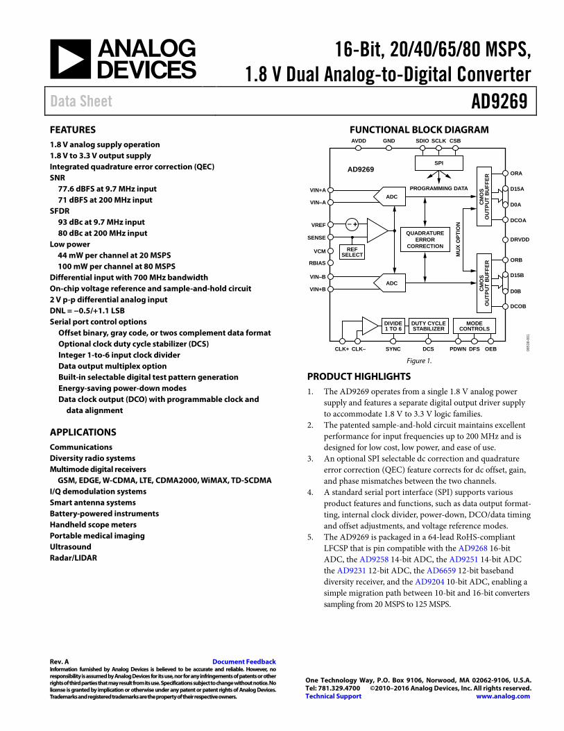
16-Bit, 20/40/65/80 MSPS, 1.8 V Dual Analog-to-Digital Converter
Data Sheet AD9269
Rev. A Document Feedback Information furnished by Analog Devices is believed to be accurate and reliable. However, no responsibility is assumed by Analog Devices for its use, nor for any infringements of patents or other rights of third parties that may result from its use. Specifications subject to change without notice. No license is granted by implication or otherwise under any patent or patent rights of Analog Devices. Trademarks and registered trademarks are the property of their respective owners.
One Technology Way, P.O. Box 9106, Norwood, MA 02062-9106, U.S.A. Tel: 781.329.4700 ©2010–2016 Analog Devices, Inc. All rights reserved. Technical Support www.analog.com
FEATURES 1.8 V analog supply operation 1.8 V to 3.3 V output supply Integrated quadrature error correction (QEC) SNR
77.6 dBFS at 9.7 MHz input 71 dBFS at 200 MHz input
SFDR 93 dBc at 9.7 MHz input 80 dBc at 200 MHz input
Low power 44 mW per channel at 20 MSPS 100 mW per channel at 80 MSPS
Differential input with 700 MHz bandwidth On-chip voltage reference and sample-and-hold circuit 2 V p-p differential analog input DNL = −0.5/+1.1 LSB Serial port control options
Offset binary, gray code, or twos complement data format Optional clock duty cycle stabilizer (DCS) Integer 1-to-6 input clock divider Data output multiplex option Built-in selectable digital test pattern generation Energy-saving power-down modes Data clock output (DCO) with programmable clock and
data alignment
APPLICATIONS Communications Diversity radio systems Multimode digital receivers
GSM, EDGE, W-CDMA, LTE, CDMA2000, WiMAX, TD-SCDMA I/Q demodulation systems Smart antenna systems Battery-powered instruments Handheld scope meters Portable medical imaging Ultrasound Radar/LIDAR
FUNCTIONAL BLOCK DIAGRAM
VIN+A
VIN–A
VREF
SENSE
VCM
RBIAS
VIN–B
VIN+B
ORA
D0A
D15A
DCOA
DRVDD
ORB
D15B
D0B
DCOB
SDIOGNDAVDD SCLK
SPI
QUADRATUREERROR
CORRECTION
PROGRAMMING DATA
MU
X O
PTIO
N
PDWN DFSCLK+ CLK–
MODECONTROLS
DCS
DUTY CYCLESTABILIZER
SYNC
DIVIDE1 TO 6
OEB
CSB
REFSELECT
ADC
CM
OS
OU
TPU
T B
UFF
ER
ADC
CM
OS
OU
TPU
T B
UFF
ER
AD9269
0853
8-00
1
Figure 1.
PRODUCT HIGHLIGHTS 1. The AD9269 operates from a single 1.8 V analog power
supply and features a separate digital output driver supply to accommodate 1.8 V to 3.3 V logic families.
2. The patented sample-and-hold circuit maintains excellent performance for input frequencies up to 200 MHz and is designed for low cost, low power, and ease of use.
3. An optional SPI selectable dc correction and quadrature error correction (QEC) feature corrects for dc offset, gain, and phase mismatches between the two channels.
4. A standard serial port interface (SPI) supports various product features and functions, such as data output format-ting, internal clock divider, power-down, DCO/data timing and offset adjustments, and voltage reference modes.
5. The AD9269 is packaged in a 64-lead RoHS-compliant LFCSP that is pin compatible with the AD9268 16-bit ADC, the AD9258 14-bit ADC, the AD9251 14-bit ADC the AD9231 12-bit ADC, the AD6659 12-bit baseband diversity receiver, and the AD9204 10-bit ADC, enabling a simple migration path between 10-bit and 16-bit converters sampling from 20 MSPS to 125 MSPS.
AD9269 Data Sheet
Rev. A | Page 2 of 40
TABLE OF CONTENTS Features .............................................................................................. 1
Applications ....................................................................................... 1
Functional Block Diagram .............................................................. 1
Product Highlights ........................................................................... 1
Revision History ............................................................................... 2
General Description ......................................................................... 3
Specifications ..................................................................................... 4
DC Specifications ......................................................................... 4
AC Specifications .......................................................................... 6
Digital Specifications ................................................................... 7
Switching Specifications .............................................................. 8
Timing Specifications .................................................................. 9
Absolute Maximum Ratings .......................................................... 10
Thermal Characteristics ............................................................ 10
ESD Caution ................................................................................ 10
Pin Configuration and Function Descriptions ........................... 11
Typical Performance Characteristics ........................................... 13
AD9269-80 .................................................................................. 13
AD9269-65 .................................................................................. 15
AD9269-40 .................................................................................. 16
AD9269-20 .................................................................................. 17
Equivalent Circuits ......................................................................... 18
Theory of Operation ...................................................................... 19
ADC Architecture ...................................................................... 19
Analog Input Considerations .................................................... 19
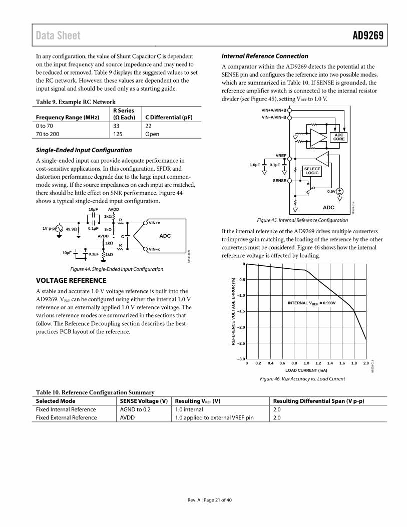
Voltage Reference ....................................................................... 21
Clock Input Considerations ...................................................... 22
Power Dissipation and Standby Mode .................................... 24
Digital Outputs ........................................................................... 25
Timing ......................................................................................... 25
Built-In Self-Test (BIST) and Output Test .................................. 26
Built-In Self-Test (BIST) ............................................................ 26
Output Test Modes ..................................................................... 26
Channel/Chip Synchronization .................................................... 27
DC and Quadrature Error Correction (QEC) ............................ 28
Serial Port Interface (SPI) .............................................................. 29
Configuration Using the SPI ..................................................... 29
Hardware Interface ..................................................................... 29
Configuration Without the SPI ................................................ 30
SPI Accessible Features .............................................................. 30
Memory Map .................................................................................. 31
Reading the Memory Map Register Table ............................... 31
Open Locations .......................................................................... 31
Default Values ............................................................................. 31
Memory Map Register Table ..................................................... 32
Memory Map Register Descriptions ........................................ 34
Applications Information .............................................................. 36
Design Guidelines ...................................................................... 36
Outline Dimensions ....................................................................... 37
Ordering Guide .......................................................................... 37
REVISION HISTORY 8/2016—Rev. 0 to Rev. A Changes to Figure 3 ................................................................................. 8 Updated Outline Dimensions ............................................................... 37 1/2010—Revision 0: Initial Version
Data Sheet AD9269
Rev. A | Page 3 of 40
GENERAL DESCRIPTION The AD9269 is a monolithic, dual-channel, 1.8 V supply, 16-bit, 20/40/65/80 MSPS analog-to-digital converter (ADC). It features a high performance sample-and-hold circuit and on-chip voltage reference.
The product uses multistage differential pipeline architecture with output error correction logic to provide 16-bit accuracy at 80 MSPS data rates and to guarantee no missing codes over the full operating temperature range.
The AD9269 incorporates an optional integrated dc correction and quadrature error correction block (QEC) that corrects for dc offset, gain, and phase mismatch between the two channels. This functional block can be very beneficial to complex signal processing applications such as direct conversion receivers.
The ADC also contains several features designed to maximize flexibility and minimize system cost, such as programmable clock and data alignment and programmable digital test pattern
generation. The available digital test patterns include built-in deterministic and pseudorandom patterns, along with custom user-defined test patterns entered via the serial port interface (SPI).
A differential clock input controls all internal conversion cycles. An optional duty cycle stabilizer (DCS) compensates for wide variations in the clock duty cycle while maintaining excellent overall ADC performance.
The digital output data is presented in offset binary, gray code, or twos complement format. A data output clock (DCO) is pro-vided for each ADC channel to ensure proper latch timing with receiving logic. Both 1.8 V and 3.3 V CMOS levels are supported, and output data can be multiplexed onto a single output bus.
The AD9269 is available in a 64-lead RoHS-compliant LFCSP and is specified over the industrial temperature range (−40°C to +85°C).
AD9269 Data Sheet
Rev. A | Page 4 of 40
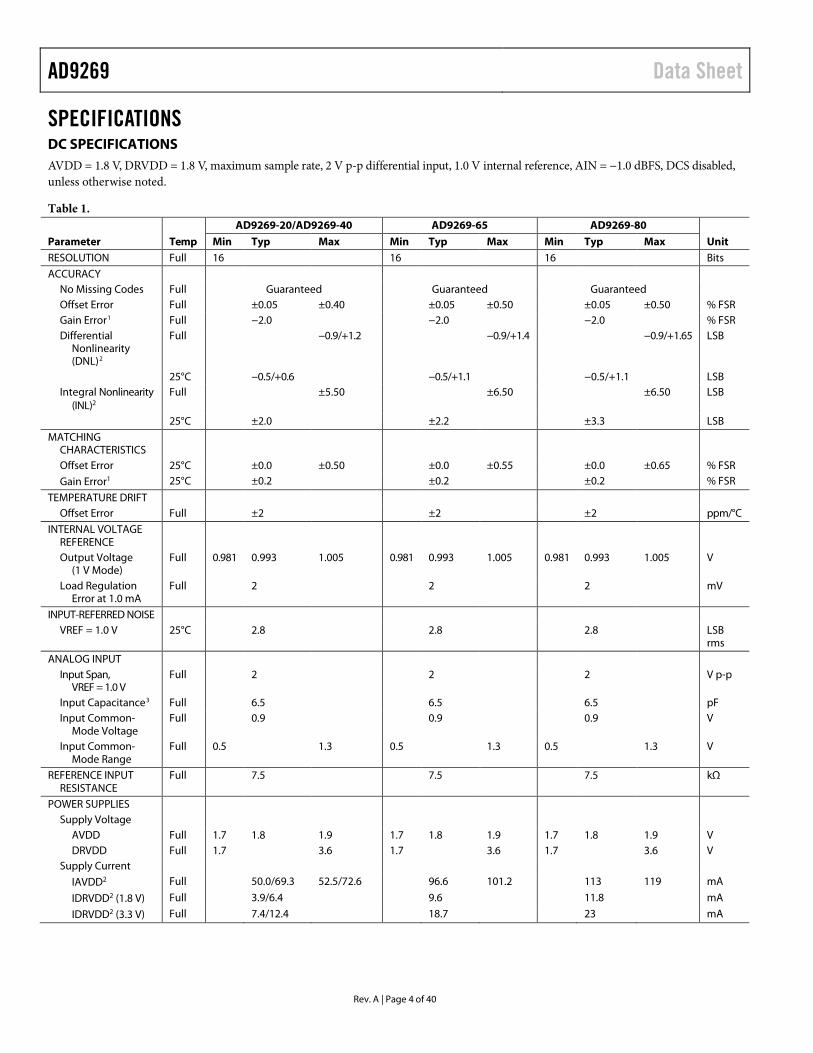
SPECIFICATIONS DC SPECIFICATIONS AVDD = 1.8 V, DRVDD = 1.8 V, maximum sample rate, 2 V p-p differential input, 1.0 V internal reference, AIN = −1.0 dBFS, DCS disabled, unless otherwise noted.
Table 1.
Parameter Temp
AD9269-20/AD9269-40 AD9269-65 AD9269-80
Unit Min Typ Max Min Typ Max Min Typ Max RESOLUTION Full 16 16 16 Bits
ACCURACY No Missing Codes Full Guaranteed Guaranteed Guaranteed Offset Error Full ±0.05 ±0.40 ±0.05 ±0.50 ±0.05 ±0.50 % FSR Gain Error1 Full −2.0 −2.0 −2.0 % FSR Differential
Nonlinearity (DNL)2
Full −0.9/+1.2 −0.9/+1.4 −0.9/+1.65 LSB
25°C −0.5/+0.6 −0.5/+1.1 −0.5/+1.1 LSB Integral Nonlinearity
(INL)2 Full ±5.50 ±6.50 ±6.50 LSB
25°C ±2.0 ±2.2 ±3.3 LSB
MATCHING CHARACTERISTICS
Offset Error 25°C ±0.0 ±0.50 ±0.0 ±0.55 ±0.0 ±0.65 % FSR
Gain Error1 25°C ±0.2 ±0.2 ±0.2 % FSR
TEMPERATURE DRIFT Offset Error Full ±2 ±2 ±2 ppm/°C
INTERNAL VOLTAGE REFERENCE
Output Voltage (1 V Mode)
Full 0.981 0.993 1.005 0.981 0.993 1.005 0.981 0.993 1.005 V
Load Regulation Error at 1.0 mA
Full 2 2 2 mV
INPUT-REFERRED NOISE VREF = 1.0 V 25°C 2.8 2.8 2.8 LSB
rms
ANALOG INPUT Input Span,
VREF = 1.0 V Full 2 2 2 V p-p
Input Capacitance3 Full 6.5 6.5 6.5 pF Input Common-
Mode Voltage Full 0.9 0.9 0.9 V
Input Common-Mode Range
Full 0.5 1.3 0.5 1.3 0.5 1.3 V
REFERENCE INPUT RESISTANCE
Full 7.5 7.5 7.5 kΩ
POWER SUPPLIES Supply Voltage
AVDD Full 1.7 1.8 1.9 1.7 1.8 1.9 1.7 1.8 1.9 V DRVDD Full 1.7 3.6 1.7 3.6 1.7 3.6 V
Supply Current
IAVDD2 Full 50.0/69.3 52.5/72.6 96.6 101.2 113 119 mA
IDRVDD2 (1.8 V) Full 3.9/6.4 9.6 11.8 mA
IDRVDD2 (3.3 V) Full 7.4/12.4 18.7 23 mA
Data Sheet AD9269
Rev. A | Page 5 of 40
Parameter Temp
AD9269-20/AD9269-40 AD9269-65 AD9269-80
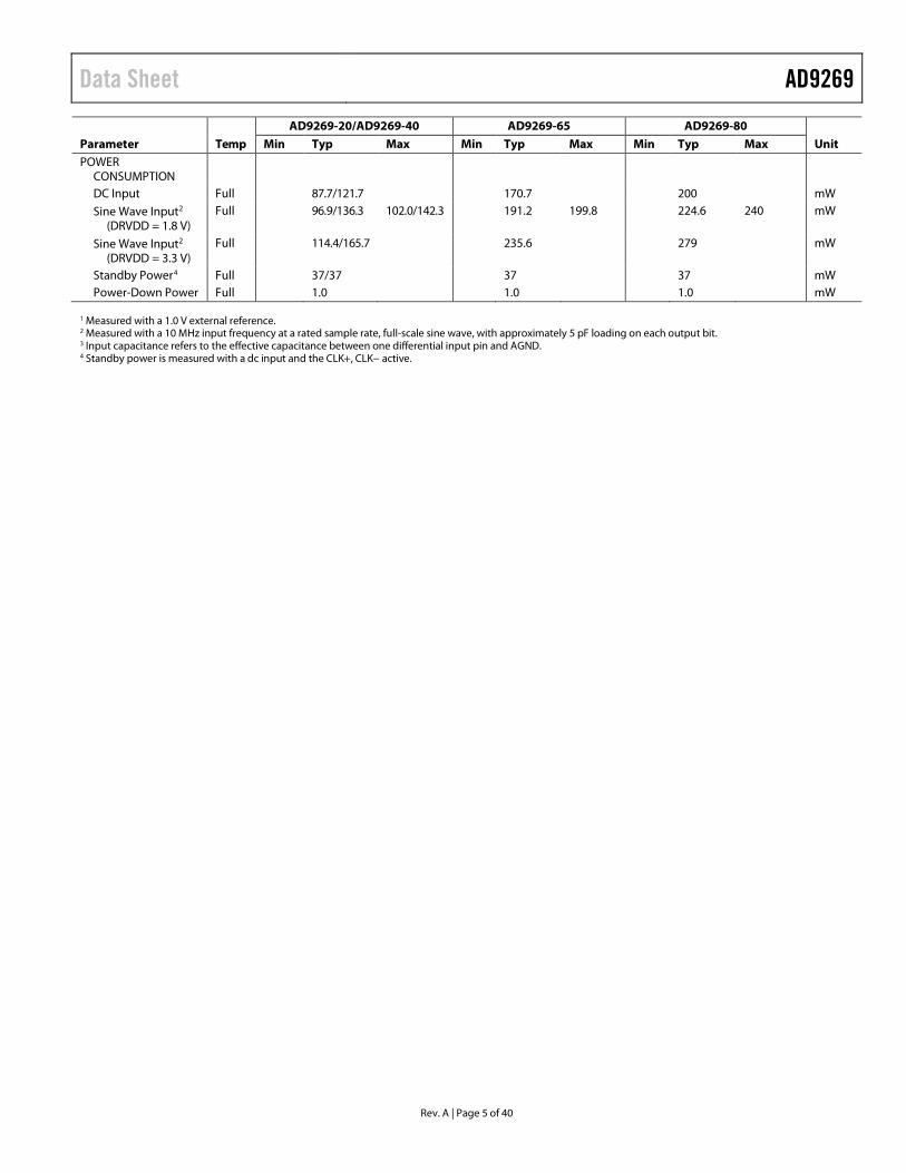
Unit Min Typ Max Min Typ Max Min Typ Max POWER
CONSUMPTION
DC Input Full 87.7/121.7 170.7 200 mW
Sine Wave Input2 (DRVDD = 1.8 V)
Full 96.9/136.3 102.0/142.3 191.2 199.8 224.6 240 mW
Sine Wave Input2 (DRVDD = 3.3 V)
Full 114.4/165.7 235.6 279 mW
Standby Power4 Full 37/37 37 37 mW Power-Down Power Full 1.0 1.0 1.0 mW
1 Measured with a 1.0 V external reference. 2 Measured with a 10 MHz input frequency at a rated sample rate, full-scale sine wave, with approximately 5 pF loading on each output bit. 3 Input capacitance refers to the effective capacitance between one differential input pin and AGND. 4 Standby power is measured with a dc input and the CLK+, CLK− active.
AD9269 Data Sheet
Rev. A | Page 6 of 40
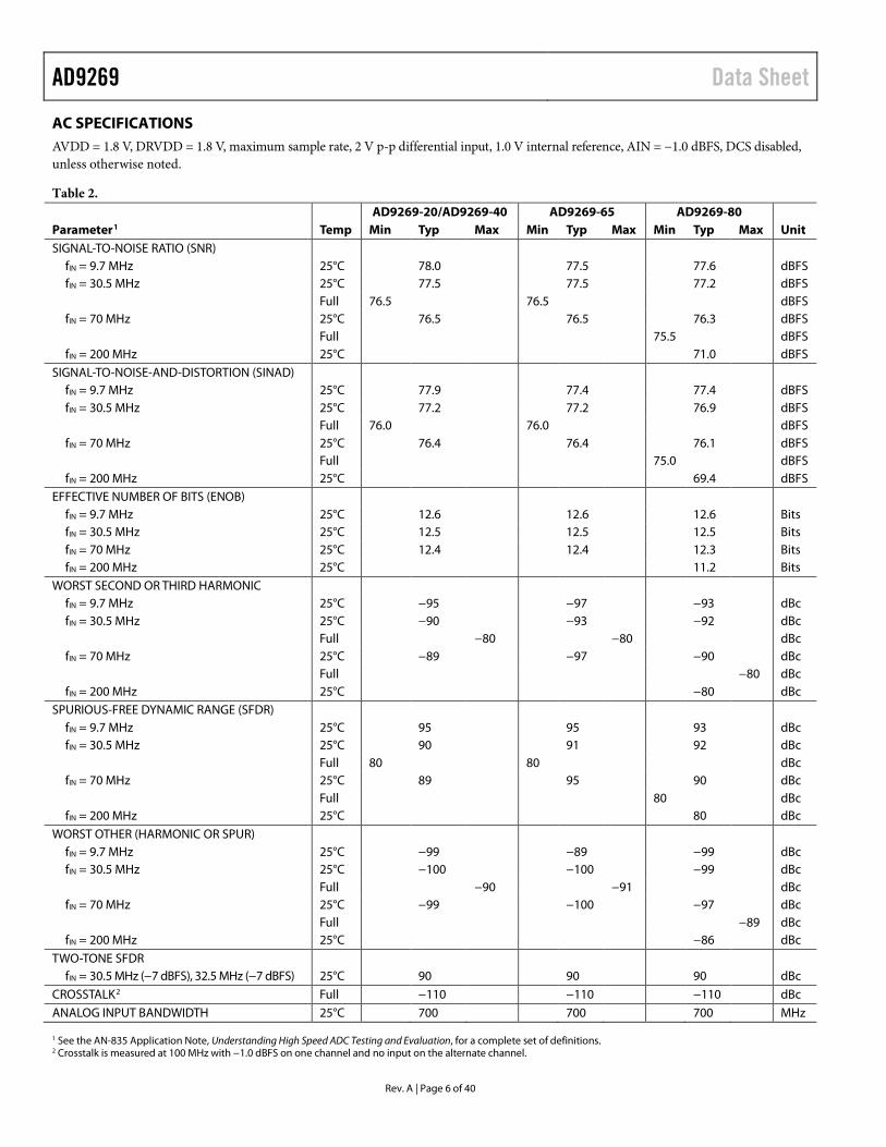
AC SPECIFICATIONS AVDD = 1.8 V, DRVDD = 1.8 V, maximum sample rate, 2 V p-p differential input, 1.0 V internal reference, AIN = −1.0 dBFS, DCS disabled, unless otherwise noted.
Table 2.
Parameter1 Temp AD9269-20/AD9269-40 AD9269-65 AD9269-80
Unit Min Typ Max Min Typ Max Min Typ Max SIGNAL-TO-NOISE RATIO (SNR)
fIN = 9.7 MHz 25°C 78.0 77.5 77.6 dBFS fIN = 30.5 MHz 25°C 77.5 77.5 77.2 dBFS Full 76.5 76.5 dBFS fIN = 70 MHz 25°C 76.5 76.5 76.3 dBFS Full 75.5 dBFS fIN = 200 MHz 25°C 71.0 dBFS
SIGNAL-TO-NOISE-AND-DISTORTION (SINAD) fIN = 9.7 MHz 25°C 77.9 77.4 77.4 dBFS fIN = 30.5 MHz 25°C 77.2 77.2 76.9 dBFS Full 76.0 76.0 dBFS fIN = 70 MHz 25°C 76.4 76.4 76.1 dBFS Full 75.0 dBFS fIN = 200 MHz 25°C 69.4 dBFS
EFFECTIVE NUMBER OF BITS (ENOB) fIN = 9.7 MHz 25°C 12.6 12.6 12.6 Bits fIN = 30.5 MHz 25°C 12.5 12.5 12.5 Bits fIN = 70 MHz 25°C 12.4 12.4 12.3 Bits fIN = 200 MHz 25°C 11.2 Bits
WORST SECOND OR THIRD HARMONIC fIN = 9.7 MHz 25°C −95 −97 −93 dBc fIN = 30.5 MHz 25°C −90 −93 −92 dBc Full −80 −80 dBc fIN = 70 MHz 25°C −89 −97 −90 dBc Full −80 dBc fIN = 200 MHz 25°C −80 dBc
SPURIOUS-FREE DYNAMIC RANGE (SFDR) fIN = 9.7 MHz 25°C 95 95 93 dBc fIN = 30.5 MHz 25°C 90 91 92 dBc Full 80 80 dBc fIN = 70 MHz 25°C 89 95 90 dBc Full 80 dBc fIN = 200 MHz 25°C 80 dBc
WORST OTHER (HARMONIC OR SPUR) fIN = 9.7 MHz 25°C −99 −89 −99 dBc fIN = 30.5 MHz 25°C −100 −100 −99 dBc Full −90 −91 dBc fIN = 70 MHz 25°C −99 −100 −97 dBc Full −89 dBc fIN = 200 MHz 25°C −86 dBc
TWO-TONE SFDR fIN = 30.5 MHz (−7 dBFS), 32.5 MHz (−7 dBFS) 25°C 90 90 90 dBc
CROSSTALK2 Full −110 −110 −110 dBc ANALOG INPUT BANDWIDTH 25°C 700 700 700 MHz 1 See the AN-835 Application Note, Understanding High Speed ADC Testing and Evaluation, for a complete set of definitions. 2 Crosstalk is measured at 100 MHz with −1.0 dBFS on one channel and no input on the alternate channel.

Data Sheet AD9269
Rev. A | Page 7 of 40
DIGITAL SPECIFICATIONS AVDD = 1.8 V, DRVDD = 1.8 V, maximum sample rate, 2 V p-p differential input, 1.0 V internal reference, AIN = −1.0 dBFS, DCS disabled, unless otherwise noted.
Table 3.
Parameter Temp AD9269-20/AD9269-40/AD9269-65/AD9269-80
Unit Min Typ Max DIFFERENTIAL CLOCK INPUTS (CLK+, CLK−)
Logic Compliance CMOS/LVDS/LVPECL Internal Common-Mode Bias Full 0.9 V Differential Input Voltage Full 0.2 3.6 V p-p Input Voltage Range Full GND − 0.3 AVDD + 0.2 V High Level Input Current Full −10 +10 µA Low Level Input Current Full −10 +10 µA Input Resistance Full 8 10 12 kΩ Input Capacitance Full 4 pF
LOGIC INPUTS (SCLK/DFS, SYNC, PDWN)1 High Level Input Voltage Full 1.2 DRVDD + 0.3 V Low Level Input Voltage Full 0 0.8 V High Level Input Current Full −50 −75 µA Low Level Input Current Full −10 +10 µA Input Resistance Full 30 kΩ Input Capacitance Full 2 pF
LOGIC INPUTS (CSB)2 High Level Input Voltage Full 1.2 DRVDD + 0.3 V Low Level Input Voltage Full 0 0.8 V High Level Input Current Full −10 +10 µA Low Level Input Current Full 40 135 µA Input Resistance Full 26 kΩ Input Capacitance Full 2 pF
LOGIC INPUTS (SDIO/DCS)2 High Level Input Voltage Full 1.2 DRVDD + 0.3 V Low Level Input Voltage Full 0 0.8 V High Level Input Current Full −10 +10 µA Low Level Input Current Full 40 130 µA Input Resistance Full 26 kΩ Input Capacitance Full 5 pF
DIGITAL OUTPUTS DRVDD = 3.3 V
High Level Output Voltage, IOH = 50 µA Full 3.29 V High Level Output Voltage, IOH = 0.5 mA Full 3.25 V Low Level Output Voltage, IOL = 1.6 mA Full 0.2 V Low Level Output Voltage, IOL = 50 µA Full 0.05 V
DRVDD = 1.8 V High Level Output Voltage, IOH = 50 µA Full 1.79 V High Level Output Voltage, IOH = 0.5 mA Full 1.75 V Low Level Output Voltage, IOL = 1.6 mA Full 0.2 V Low Level Output Voltage, IOL = 50 µA Full 0.05 V
1 Internal 30 kΩ pull-down. 2 Internal 30 kΩ pull-up.
AD9269 Data Sheet
Rev. A | Page 8 of 40
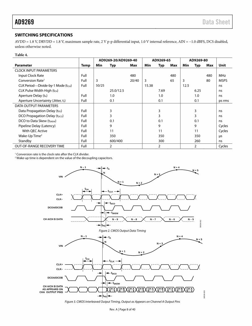
SWITCHING SPECIFICATIONS AVDD = 1.8 V, DRVDD = 1.8 V, maximum sample rate, 2 V p-p differential input, 1.0 V internal reference, AIN = −1.0 dBFS, DCS disabled, unless otherwise noted.
Table 4.
Parameter Temp AD9269-20/AD9269-40 AD9269-65 AD9269-80
Unit Min Typ Max Min Typ Max Min Typ Max CLOCK INPUT PARAMETERS
Input Clock Rate Full 480 480 480 MHz Conversion Rate1 Full 3 20/40 3 65 3 80 MSPS CLK Period—Divide-by-1 Mode (tCLK) Full 50/25 15.38 12.5 ns CLK Pulse Width High (tCH) 25.0/12.5 7.69 6.25 ns Aperture Delay (tA) Full 1.0 1.0 1.0 ns Aperture Uncertainty (Jitter, tJ) Full 0.1 0.1 0.1 ps rms
DATA OUTPUT PARAMETERS Data Propagation Delay (tPD) Full 3 3 3 ns DCO Propagation Delay (tDCO) Full 3 3 3 ns DCO to Data Skew (tSKEW) Full 0.1 0.1 0.1 ns Pipeline Delay (Latency) Full 9 9 9 Cycles
With QEC Active Full 11 11 11 Cycles Wake-Up Time2 Full 350 350 350 μs Standby Full 600/400 300 260 ns
OUT-OF-RANGE RECOVERY TIME Full 2 2 2 Cycles 1 Conversion rate is the clock rate after the CLK divider. 2 Wake-up time is dependent on the value of the decoupling capacitors.
tPD
tSKEW
tCH
tDCO
tCLK
N – 9
N – 1
N + 1 N + 2
N + 3N + 5
N + 4
N
N – 8 N – 7 N – 6 N – 5
VIN
CLK+
CLK–
CH A/CH B DATA
DCOA/DCOB
tA
0853
8-00
2
Figure 2. CMOS Output Data Timing
tPD
tSKEW
tCH
tDCO
tCLK
CH AN – 9
CH BN – 9
CH AN – 8
CH BN – 8
CH AN – 7
CH BN – 7
CH AN – 6
CH BN – 6
CH AN – 5
N – 1
N + 1 N + 2
N + 3N + 5
N + 4
NVIN
CLK+
CLK–
CH A/CH B DATAAS APPEARS ON
CHA OUTPUT PINS
DCOA/DCOB
tA
0853
8-00
3
Figure 3. CMOS Interleaved Output Timing, Output as Appears on Channel A Output Pins
Data Sheet AD9269
Rev. A | Page 9 of 40
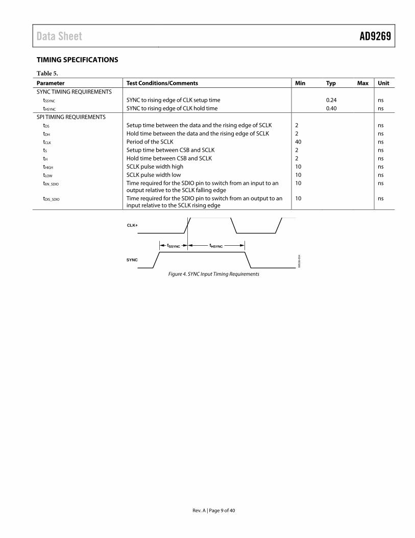
TIMING SPECIFICATIONS
Table 5. Parameter Test Conditions/Comments Min Typ Max Unit SYNC TIMING REQUIREMENTS
tSSYNC SYNC to rising edge of CLK setup time 0.24 ns tHSYNC SYNC to rising edge of CLK hold time 0.40 ns
SPI TIMING REQUIREMENTS tDS Setup time between the data and the rising edge of SCLK 2 ns tDH Hold time between the data and the rising edge of SCLK 2 ns tCLK Period of the SCLK 40 ns tS Setup time between CSB and SCLK 2 ns tH Hold time between CSB and SCLK 2 ns tHIGH SCLK pulse width high 10 ns tLOW SCLK pulse width low 10 ns tEN_SDIO Time required for the SDIO pin to switch from an input to an
output relative to the SCLK falling edge 10 ns
tDIS_SDIO Time required for the SDIO pin to switch from an output to an input relative to the SCLK rising edge
10 ns
SYNC
CLK+
tHSYNCtSSYNC
0853
8-00
4
Figure 4. SYNC Input Timing Requirements
AD9269 Data Sheet
Rev. A | Page 10 of 40
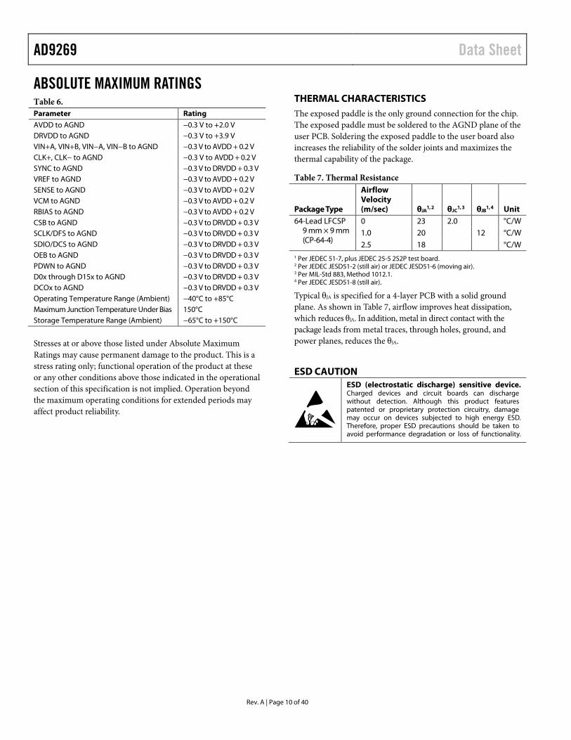
ABSOLUTE MAXIMUM RATINGS Table 6. Parameter Rating
AVDD to AGND −0.3 V to +2.0 V DRVDD to AGND −0.3 V to +3.9 V VIN+A, VIN+B, VIN−A, VIN−B to AGND −0.3 V to AVDD + 0.2 V CLK+, CLK− to AGND −0.3 V to AVDD + 0.2 V SYNC to AGND −0.3 V to DRVDD + 0.3 V VREF to AGND −0.3 V to AVDD + 0.2 V SENSE to AGND −0.3 V to AVDD + 0.2 V VCM to AGND −0.3 V to AVDD + 0.2 V RBIAS to AGND −0.3 V to AVDD + 0.2 V CSB to AGND −0.3 V to DRVDD + 0.3 V SCLK/DFS to AGND −0.3 V to DRVDD + 0.3 V SDIO/DCS to AGND −0.3 V to DRVDD + 0.3 V OEB to AGND −0.3 V to DRVDD + 0.3 V PDWN to AGND −0.3 V to DRVDD + 0.3 V D0x through D15x to AGND −0.3 V to DRVDD + 0.3 V DCOx to AGND −0.3 V to DRVDD + 0.3 V Operating Temperature Range (Ambient) −40°C to +85°C Maximum Junction Temperature Under Bias 150°C Storage Temperature Range (Ambient) −65°C to +150°C
Stresses at or above those listed under Absolute Maximum Ratings may cause permanent damage to the product. This is a stress rating only; functional operation of the product at these or any other conditions above those indicated in the operational section of this specification is not implied. Operation beyond the maximum operating conditions for extended periods may affect product reliability.
THERMAL CHARACTERISTICS The exposed paddle is the only ground connection for the chip. The exposed paddle must be soldered to the AGND plane of the user PCB. Soldering the exposed paddle to the user board also increases the reliability of the solder joints and maximizes the thermal capability of the package.
Table 7. Thermal Resistance
Package Type
Airflow Velocity (m/sec) θJA
1, 2 θJC1, 3 θJB
1, 4 Unit 64-Lead LFCSP
9 mm × 9 mm (CP-64-4)
0 23 2.0 °C/W 1.0 20 12 °C/W 2.5 18 °C/W
1 Per JEDEC 51-7, plus JEDEC 25-5 2S2P test board. 2 Per JEDEC JESD51-2 (still air) or JEDEC JESD51-6 (moving air). 3 Per MIL-Std 883, Method 1012.1. 4 Per JEDEC JESD51-8 (still air).
Typical θJA is specified for a 4-layer PCB with a solid ground plane. As shown in Table 7, airflow improves heat dissipation, which reduces θJA. In addition, metal in direct contact with the package leads from metal traces, through holes, ground, and power planes, reduces the θJA.
ESD CAUTION
Data Sheet AD9269
Rev. A | Page 11 of 40
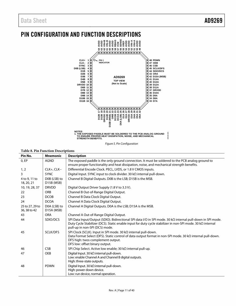
PIN CONFIGURATION AND FUNCTION DESCRIPTIONS
PIN 1INDICATOR
17 18 19 20 21 22 23 24 25 26 27 28 29 30 31 32
D12
BD
13B
DR
VDD
D14
BD
15B
(MSB
)O
RB
DC
OB
DC
OA
D0 A
(LSB
)D
1AD
2AD
RVD
DD
3 AD
4AD
5AD
6 A
64 63 62 61 60 59 58 57 56 55 54 53 52 51 50 49
AVD
DAV
DD
VIN
+BVI
N–B
AVD
DA V
DD
RB
IAS
VCM
SEN
SEVR
EFAV
DD
AVD
DVI
N– A
VIN
+AAV
DD
AVD
D
123456789
10111213141516
CLK+CLK–SYNC
D0B (LSB)D1BD2BD3BD4BD5B
DRVDDD6BD7BD8BD9B
D10BD11B
PDWNOEBCSBSCLK/DFSSDIO/DCSORAD15A (MSB)D14AD13AD12AD11ADRVDDD10AD9AD8AD7A
48474645444342414039383736353433
AD9269TOP VIEW
(Not to Scale)
0853
8-00
5NOTES1. THE EXPOSED PADDLE MUST BE SOLDERED TO THE PCB ANALOG GROUND
TO ENSURE PROPER HEAT DISSIPATION, NOISE, AND MECHANICALSTRENGTH BENEFITS.
Figure 5. Pin Configuration
Table 8. Pin Function Descriptions Pin No. Mnemonic Description 0, EP AGND The exposed paddle is the only ground connection. It must be soldered to the PCB analog ground to
ensure proper functionality and heat dissipation, noise, and mechanical strength benefits. 1, 2 CLK+, CLK− Differential Encode Clock. PECL, LVDS, or 1.8 V CMOS inputs. 3 SYNC Digital Input. SYNC input to clock divider. 30 kΩ internal pull-down. 4 to 9, 11 to 18, 20, 21
D0B (LSB) to D15B (MSB)
Channel B Digital Outputs. D0B is the LSB; D15B is the MSB.
10, 19, 28, 37 DRVDD Digital Output Driver Supply (1.8 V to 3.3 V). 22 ORB Channel B Out-of-Range Digital Output. 23 DCOB Channel B Data Clock Digital Output. 24 DCOA Channel A Data Clock Digital Output. 25 to 27, 29 to 36, 38 to 42
D0A (LSB) to D15A (MSB)
Channel A Digital Outputs. D0A is the LSB; D15A is the MSB.
43 ORA Channel A Out-of-Range Digital Output. 44 SDIO/DCS SPI Data Input/Output (SDIO). Bidirectional SPI data I/O in SPI mode. 30 kΩ internal pull-down in SPI mode.
Duty Cycle Stabilizer (DCS). Static enable input for duty cycle stabilizer in non-SPI mode. 30 kΩ internal pull-up in non-SPI (DCS) mode.
45 SCLK/DFS SPI Clock (SCLK). Input in SPI mode. 30 kΩ internal pull-down. Data Format Select (DFS). Static control of data output format in non-SPI mode. 30 kΩ internal pull-down. DFS high: twos complement output. DFS low: offset binary output.
46 CSB SPI Chip Select. Active low enable; 30 kΩ internal pull-up. 47 OEB Digital Input. 30 kΩ internal pull-down.
Low: enable Channel A and Channel B digital outputs. High: three-state outputs.
48 PDWN Digital Input. 30 kΩ internal pull-down. High: power down device. Low: run device, normal operation.
AD9269 Data Sheet
Rev. A | Page 12 of 40
Pin No. Mnemonic Description 49, 50, 53, 54, 59, 60, 63, 64
AVDD 1.8 V Analog Supply Pins.
51, 52 VIN+A, VIN−A Channel A Analog Inputs. 55 VREF Voltage Reference Input/Output. 56 SENSE Reference Mode Selection. 57 VCM Analog Output Voltage at Midsupply. Sets the common mode of the analog inputs. 58 RBIAS Set Analog Current Bias. Connect to 10 kΩ (1% tolerance) resistor to ground. 61, 62 VIN−B, VIN+B Channel B Analog Inputs.
Data Sheet AD9269
Rev. A | Page 13 of 40
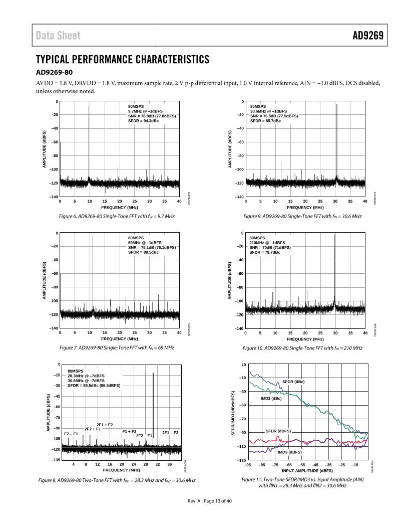
TYPICAL PERFORMANCE CHARACTERISTICS AD9269-80 AVDD = 1.8 V, DRVDD = 1.8 V, maximum sample rate, 2 V p-p differential input, 1.0 V internal reference, AIN = −1.0 dBFS, DCS disabled, unless otherwise noted.
0
–140
–20
–40
–60
–80
–100
–120
0 5 10 15 20 25 30 35 40
AM
PLIT
UD
E (d
BFS
)
FREQUENCY (MHz)
0853
8-03
3
80MSPS9.7MHz @ –1dBFSSNR = 76.8dB (77.8dBFS)SFDR = 94.3dBc
Figure 6. AD9269-80 Single-Tone FFT with fIN = 9.7 MHz
0
–140
–20
–40
–60
–80
–100
–120
0 5 10 15 20 25 30 35 40
AM
PLIT
UD
E (d
BFS
)
FREQUENCY (MHz)
0853
8-03
5
80MSPS69MHz @ –1dBFSSNR = 75.1dB (76.1dBFS)SFDR = 89.5dBc
Figure 7. AD9269-80 Single-Tone FFT with fIN = 69 MHz
0
–15
–30
–45
–60
–90
–75
–105
–120
–1354 8 12 16 20 24 28 32 36
FREQUENCY (MHz)
AM
PLIT
UD
E (d
BFS
)
0853
8-05
3
F2 – F1 F1 + F2 2F1 – F22F2 + F1
2F1 + F2
2F2 – F1
80MSPS28.3MHz @ –7dBFS30.6MHz @ –7dBFSSFDR = 89.5dBc (96.5dBFS)
Figure 8. AD9269-80 Two-Tone FFT with fIN1 = 28.3 MHz and fIN2 = 30.6 MHz
0
–140
–20
–40
–60
–80
–100
–120
0 5 10 15 20 25 30 35 40
AM
PLIT
UD
E (d
BFS
)
FREQUENCY (MHz)
0853
8-03
4
80MSPS30.6MHz @ –1dBFSSNR = 76.5dB (77.5dBFS)SFDR = 85.7dBc
Figure 9. AD9269-80 Single-Tone FFT with fIN = 30.6 MHz
0
–140
–20
–40
–60
–80
–100
–120
0 5 10 15 20 25 30 35 40
AM
PLIT
UD
E (d
BFS
)
FREQUENCY (MHz)
0853
8-03
6
80MSPS210MHz @ –1dBFSSNR = 70dB (71dBFS)SFDR = 79.7dBc
Figure 10. AD9269-80 Single-Tone FFT with fIN = 210 MHz
10
–30
–10
–50
–70
–90
–110
–130–95 –65–75–85 –55 –45 –35 –25 –15
INPUT AMPLITUDE (dBFS)
SFD
R/IM
D3
(dB
c/dB
FS)
0853
8-05
4
SFDR (dBc)
SFDR (dBFS)
IMD3 (dBc)
IMD3 (dBFS)
Figure 11. Two-Tone SFDR/IMD3 vs. Input Amplitude (AIN)
with fIN1 = 28.3 MHz and fIN2 = 30.6 MHz
AD9269 Data Sheet
Rev. A | Page 14 of 40
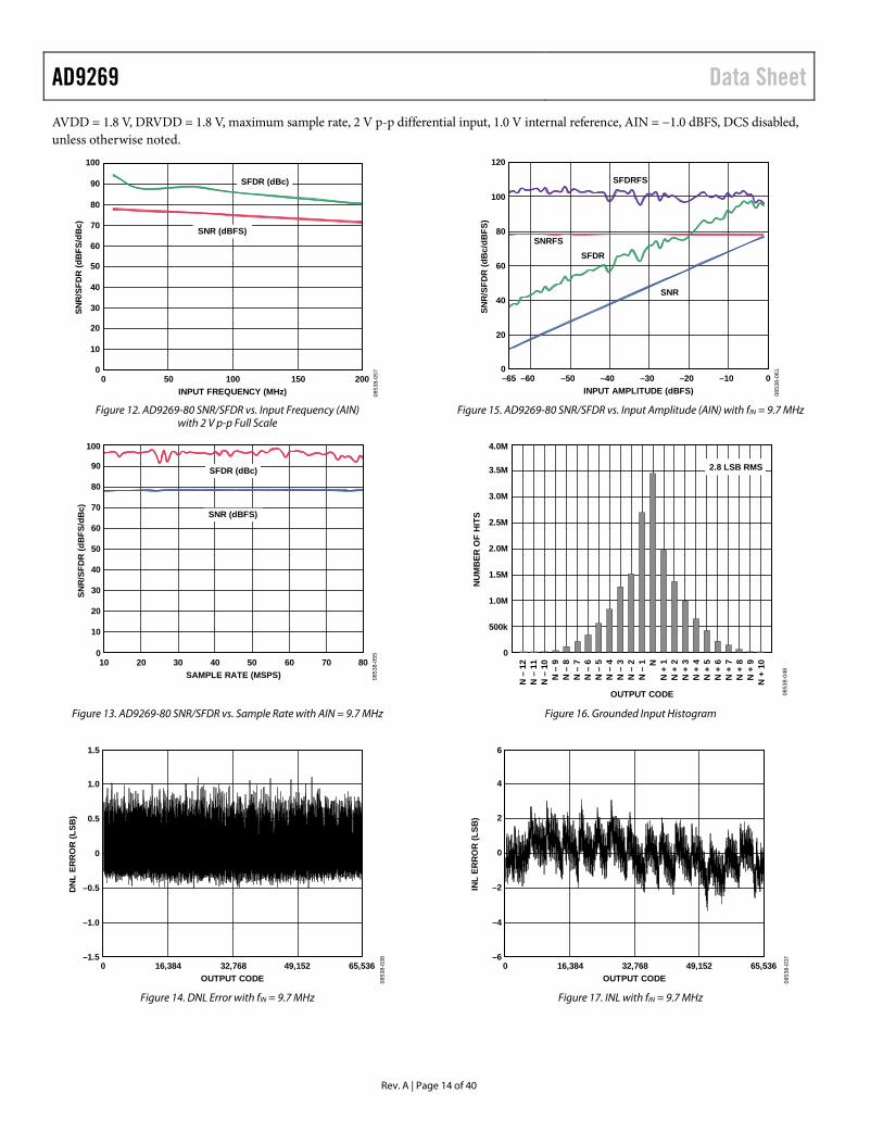
AVDD = 1.8 V, DRVDD = 1.8 V, maximum sample rate, 2 V p-p differential input, 1.0 V internal reference, AIN = −1.0 dBFS, DCS disabled, unless otherwise noted.
100
90
80
70
60
50
40
30
20
10
00 50 100 150 200
INPUT FREQUENCY (MHz)
SNR
/SFD
R (d
BFS
/dB
c)
0853
8-05
7
SFDR (dBc)
SNR (dBFS)
Figure 12. AD9269-80 SNR/SFDR vs. Input Frequency (AIN)
with 2 V p-p Full Scale
100
90
80
70
30
40
50
60
20
10
010 20 30 40 50 60 70 80
SAMPLE RATE (MSPS)
SNR
/SFD
R (d
BFS
/dB
c)
0853
8-05
5
SFDR (dBc)
SNR (dBFS)
Figure 13. AD9269-80 SNR/SFDR vs. Sample Rate with AIN = 9.7 MHz
1.5
1.0
0.5
–0.5
0
–1.0
–1.50 16,384 32,768 49,152 65,536
OUTPUT CODE
DN
L ER
RO
R (L
SB)
0853
8-03
8
Figure 14. DNL Error with fIN = 9.7 MHz
120
0
20
40
60
80
100
–65 –60 0–10–20–30–40–50INPUT AMPLITUDE (dBFS)
SNR
/SFD
R (d
Bc/
dBFS
)
0853
8-06
1
SNR
SNRFSSFDR
SFDRFS
Figure 15. AD9269-80 SNR/SFDR vs. Input Amplitude (AIN) with fIN = 9.7 MHz
4.0M
0
500k
1.0M
1.5M
2.0M
2.5M
3.0M
3.5MN
UM
BER
OF
HIT
S
OUTPUT CODE 0853
8-04
8
N +
10
N +
9N
+ 8
N +
7N
+ 6
N +
5N
+ 4
N +
3N
+ 2
N +
1NN
– 1
N –
2N
– 3
N –
4N
– 5
N –
6N
– 7
N –
8N
– 9
N –
10
N –
11
N –
12
2.8 LSB RMS
Figure 16. Grounded Input Histogram
0
6
4
2
–2
–4
–60 16,384 32,768 49,152 65,536
OUTPUT CODE
INL
ERR
OR
(LSB
)
0853
8-03
7
Figure 17. INL with fIN = 9.7 MHz
Data Sheet AD9269
Rev. A | Page 15 of 40
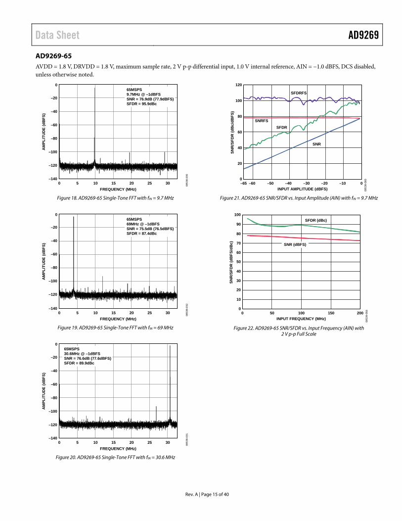
AD9269-65 AVDD = 1.8 V, DRVDD = 1.8 V, maximum sample rate, 2 V p-p differential input, 1.0 V internal reference, AIN = −1.0 dBFS, DCS disabled, unless otherwise noted.
0
–140
–120
–100
–80
–60
–40
–20
0 30252015105
AM
PLIT
UD
E (d
BFS
)
FREQUENCY (MHz)08
538-
030
65MSPS9.7MHz @ –1dBFSSNR = 76.9dB (77.9dBFS)SFDR = 95.9dBc
Figure 18. AD9269-65 Single-Tone FFT with fIN = 9.7 MHz
0
–140
–120
–100
–80
–60
–40
–20
0 30252015105
AM
PLIT
UD
E (d
BFS
)
FREQUENCY (MHz)
0853
8-03
2
65MSPS69MHz @ –1dBFSSNR = 75.5dB (76.5dBFS)SFDR = 87.4dBc
Figure 19. AD9269-65 Single-Tone FFT with fIN = 69 MHz
0
–140
–120
–100
–80
–60
–40
–20
0 30252015105
AM
PLIT
UD
E (d
BFS
)
FREQUENCY (MHz)
0853
8-03
1
65MSPS30.6MHz @ –1dBFSSNR = 76.6dB (77.6dBFS)SFDR = 89.9dBc
Figure 20. AD9269-65 Single-Tone FFT with fIN = 30.6 MHz
120
0
20
40
60
80
100
–65 –60 0–10–20–30–40–50INPUT AMPLITUDE (dBFS)
SNR
/SFD
R (d
Bc/
dBFS
)
0853
8-06
0
SNR
SNRFSSFDR
SFDRFS
Figure 21. AD9269-65 SNR/SFDR vs. Input Amplitude (AIN) with fIN = 9.7 MHz
100
90
80
70
60
50
40
30
20
10
00 50 100 150 200
INPUT FREQUENCY (MHz)
SNR
/SFD
R (d
BFS
/dB
c)
SFDR (dBc)
SNR (dBFS)
0853
9-05
6
Figure 22. AD9269-65 SNR/SFDR vs. Input Frequency (AIN) with
2 V p-p Full Scale
AD9269 Data Sheet
Rev. A | Page 16 of 40
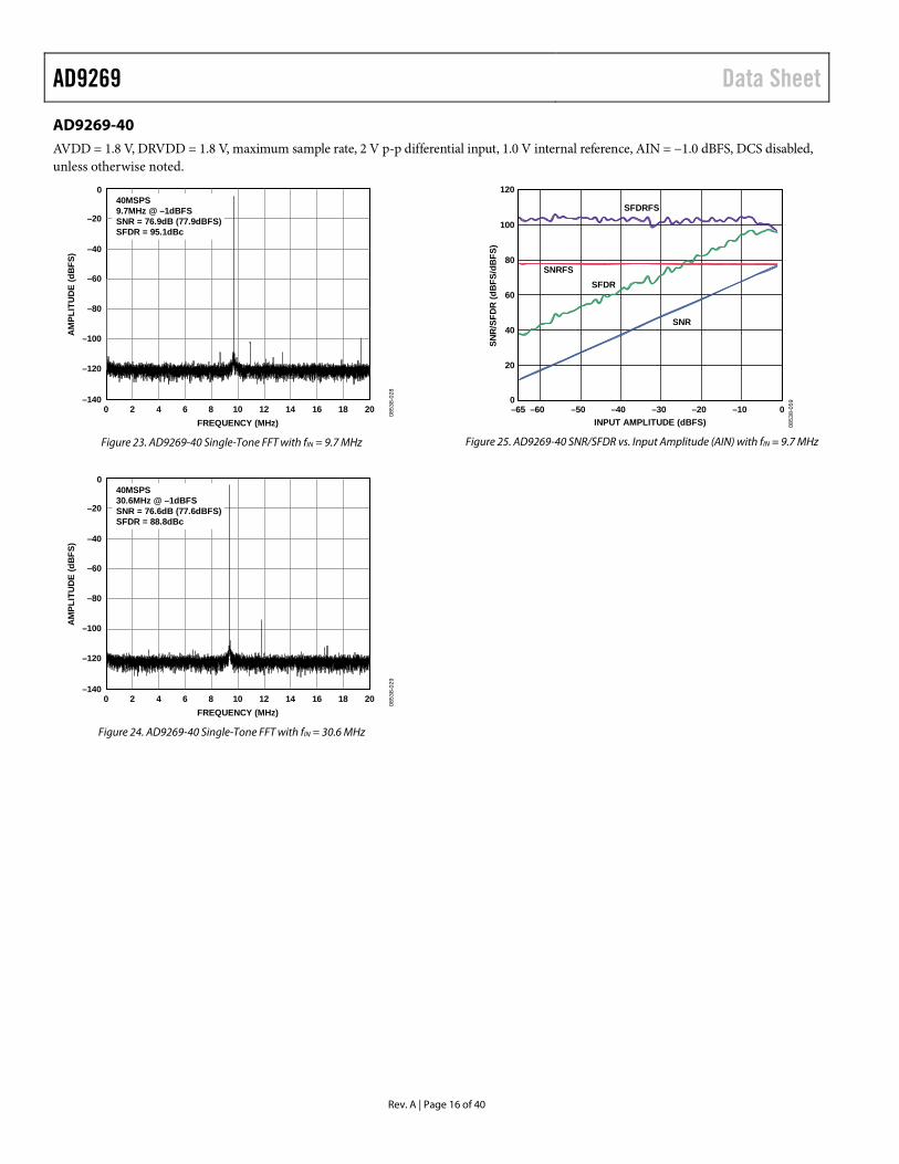
AD9269-40 AVDD = 1.8 V, DRVDD = 1.8 V, maximum sample rate, 2 V p-p differential input, 1.0 V internal reference, AIN = −1.0 dBFS, DCS disabled, unless otherwise noted.
0
–140
–120
–100
–80
–60
–40
–20
0 2 4 6 8 10 12 14 16 18 20
AM
PLIT
UD
E (d
BFS
)
FREQUENCY (MHz)
0853
8-02
8
40MSPS9.7MHz @ –1dBFSSNR = 76.9dB (77.9dBFS)SFDR = 95.1dBc
Figure 23. AD9269-40 Single-Tone FFT with fIN = 9.7 MHz
0
–140
–120
–100
–80
–60
–40
–20
0 2 4 6 8 10 12 14 16 18 20
AM
PLIT
UD
E (d
BFS
)
FREQUENCY (MHz)
0853
8-02
9
40MSPS30.6MHz @ –1dBFSSNR = 76.6dB (77.6dBFS)SFDR = 88.8dBc
Figure 24. AD9269-40 Single-Tone FFT with fIN = 30.6 MHz
120
0
20
40
60
80
100
–65 –60 0–10–20–30–40–50INPUT AMPLITUDE (dBFS)
SNR
/SFD
R (d
BFS
/dB
FS)
0853
8-05
9
SNR
SNRFSSFDR
SFDRFS
Figure 25. AD9269-40 SNR/SFDR vs. Input Amplitude (AIN) with fIN = 9.7 MHz

Data Sheet AD9269
Rev. A | Page 17 of 40
AD9269-20 AVDD = 1.8 V, DRVDD = 1.8 V, maximum sample rate, 2 V p-p differential input, 1.0 V internal reference, AIN = −1.0 dBFS, DCS disabled, unless otherwise noted.
0
–140
–120
–100
–80
–60
–40
–20
0 1 2 3 4 5 6 7 8 9 10
AM
PLIT
UD
E (d
BFS
)
FREQUENCY (MHz)08
538-
024
20MSPS9.7MHz @ –1dBFSSNR = 76.9dB (77.9dBFS)SFDR = 95.6dBc
Figure 26. AD9269-20 Single-Tone FFT with fIN = 9.7 MHz
0
–140
–120
–100
–80
–60
–40
–20
0 1 2 3 4 5 6 7 8 9 10
AM
PLIT
UD
E (d
BFS
)
FREQUENCY (MHz)
0853
8-02
6
20MSPS30.6MHz @ –1dBFSSNR = 76.7dB (77.7dBFS)SFDR = 90.7dBc
Figure 27. AD9269-20 Single-Tone FFT with fIN = 30.6 MHz
120
100
80
60
40
20
0–90 –80 –70 –60 –50 –40 –30 –20 –10 0
INPUT AMPLITUDE (dBFS)
SNR
/SFD
R (d
Bc/
dBFS
)
0853
8-05
8
SFDRFS
SNRFS
SFDR (dBc)
SNR (dBc)
Figure 28. AD9269-20 SNR/SFDR vs. Input Amplitude (AIN) with fIN = 9.7 MHz

AD9269 Data Sheet
Rev. A | Page 18 of 40
EQUIVALENT CIRCUITS AVDD
VIN±x
0853
8-03
9
Figure 29. Equivalent Analog Input Circuit
30kΩ
30kΩ
SDIO/DCS350Ω
AVDD
DRVDD
0853
8-04
1
Figure 30. Equivalent SDIO/DCS Input Circuit
350Ω
DRVDD
30kΩ
SCLK/DFS, SYNC,OEB, AND PDWN
0853
8-04
3
Figure 31. Equivalent SCLK/DFS, SYNC, OEB, and PDWN Input Circuit
7.5kΩ
VREF375Ω
AVDD
0853
8-04
7
Figure 32. Equivalent VREF Circuit
CLK+
CLK–
0.9V
15kΩ
5Ω
5Ω
15kΩ
0853
8-04
0
AVDD
AVDD
Figure 33. Equivalent Clock Input Circuit
DRVDD
0853
8-04
2
Figure 34. Equivalent Digital Output Circuit
RBIASAND VCM
375Ω
AVDD
0853
8-04
4
Figure 35. Equivalent RBIAS, VCM Circuit
30kΩ
CSB350Ω
AVDD
DRVDD
0853
8-04
5
Figure 36. Equivalent CSB Input Circuit
SENSE375Ω
AVDD
0853
8-04
6
Figure 37. Equivalent SENSE Circuit
Data Sheet AD9269
Rev. A | Page 19 of 40
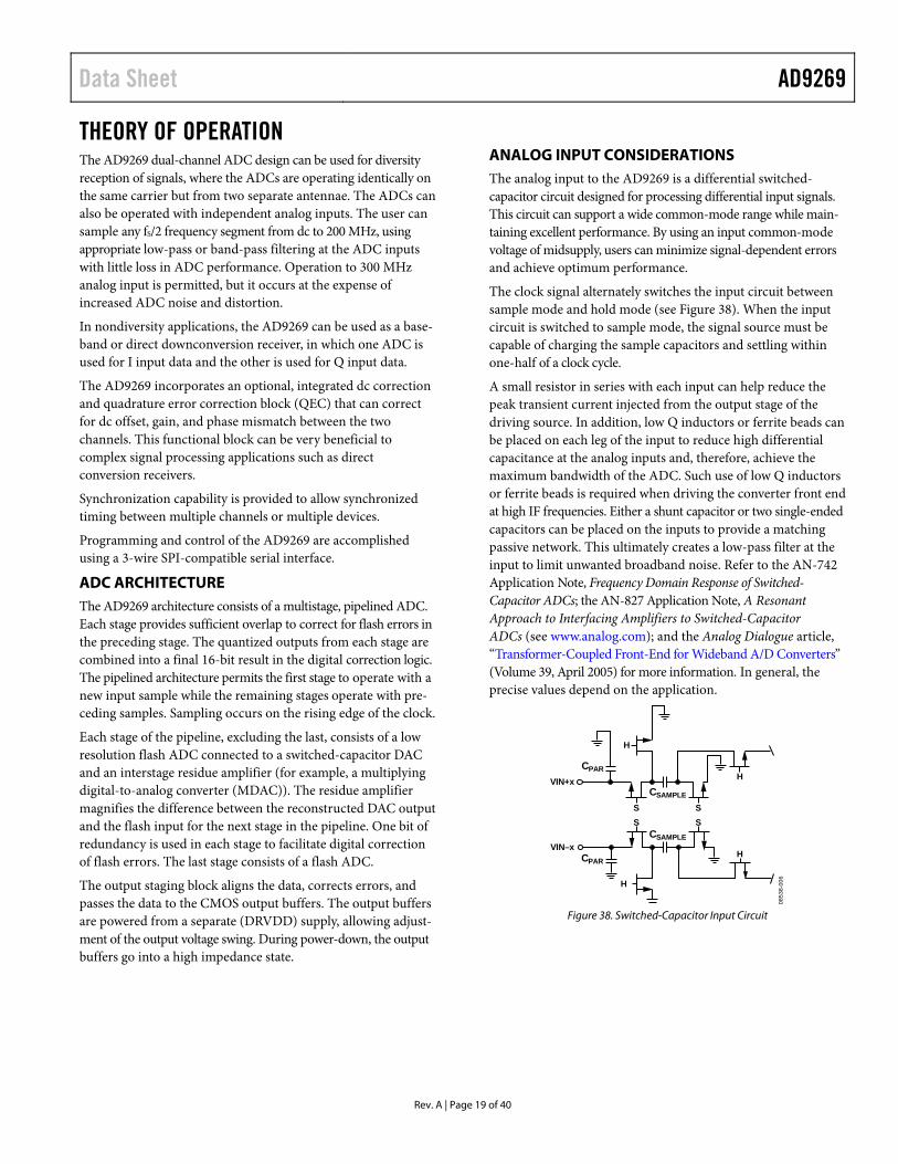
THEORY OF OPERATION The AD9269 dual-channel ADC design can be used for diversity reception of signals, where the ADCs are operating identically on the same carrier but from two separate antennae. The ADCs can also be operated with independent analog inputs. The user can sample any fS/2 frequency segment from dc to 200 MHz, using appropriate low-pass or band-pass filtering at the ADC inputs with little loss in ADC performance. Operation to 300 MHz analog input is permitted, but it occurs at the expense of increased ADC noise and distortion.
In nondiversity applications, the AD9269 can be used as a base-band or direct downconversion receiver, in which one ADC is used for I input data and the other is used for Q input data.
The AD9269 incorporates an optional, integrated dc correction and quadrature error correction block (QEC) that can correct for dc offset, gain, and phase mismatch between the two channels. This functional block can be very beneficial to complex signal processing applications such as direct conversion receivers.
Synchronization capability is provided to allow synchronized timing between multiple channels or multiple devices.
Programming and control of the AD9269 are accomplished using a 3-wire SPI-compatible serial interface.
ADC ARCHITECTURE The AD9269 architecture consists of a multistage, pipelined ADC. Each stage provides sufficient overlap to correct for flash errors in the preceding stage. The quantized outputs from each stage are combined into a final 16-bit result in the digital correction logic. The pipelined architecture permits the first stage to operate with a new input sample while the remaining stages operate with pre-ceding samples. Sampling occurs on the rising edge of the clock.
Each stage of the pipeline, excluding the last, consists of a low resolution flash ADC connected to a switched-capacitor DAC and an interstage residue amplifier (for example, a multiplying digital-to-analog converter (MDAC)). The residue amplifier magnifies the difference between the reconstructed DAC output and the flash input for the next stage in the pipeline. One bit of redundancy is used in each stage to facilitate digital correction of flash errors. The last stage consists of a flash ADC.
The output staging block aligns the data, corrects errors, and passes the data to the CMOS output buffers. The output buffers are powered from a separate (DRVDD) supply, allowing adjust-ment of the output voltage swing. During power-down, the output buffers go into a high impedance state.
ANALOG INPUT CONSIDERATIONS The analog input to the AD9269 is a differential switched-capacitor circuit designed for processing differential input signals. This circuit can support a wide common-mode range while main-taining excellent performance. By using an input common-mode voltage of midsupply, users can minimize signal-dependent errors and achieve optimum performance.
The clock signal alternately switches the input circuit between sample mode and hold mode (see Figure 38). When the input circuit is switched to sample mode, the signal source must be capable of charging the sample capacitors and settling within one-half of a clock cycle.
A small resistor in series with each input can help reduce the peak transient current injected from the output stage of the driving source. In addition, low Q inductors or ferrite beads can be placed on each leg of the input to reduce high differential capacitance at the analog inputs and, therefore, achieve the maximum bandwidth of the ADC. Such use of low Q inductors or ferrite beads is required when driving the converter front end at high IF frequencies. Either a shunt capacitor or two single-ended capacitors can be placed on the inputs to provide a matching passive network. This ultimately creates a low-pass filter at the input to limit unwanted broadband noise. Refer to the AN-742 Application Note, Frequency Domain Response of Switched-Capacitor ADCs; the AN-827 Application Note, A Resonant Approach to Interfacing Amplifiers to Switched-Capacitor ADCs (see www.analog.com); and the Analog Dialogue article, “Transformer-Coupled Front-End for Wideband A/D Converters” (Volume 39, April 2005) for more information. In general, the precise values depend on the application.
S S
HCPAR
CSAMPLE
CSAMPLE
CPAR
VIN–x
H
S S
HVIN+x
H
0853
8-00
6
Figure 38. Switched-Capacitor Input Circuit
AD9269 Data Sheet
Rev. A | Page 20 of 40
Input Common Mode
The analog inputs of the AD9269 are not internally dc-biased. Therefore, in ac-coupled applications, the user must provide a dc bias externally. Setting the device so that VCM = AVDD/2 is recommended for optimum performance, but the device can function over a wider range with reasonable performance, as shown in Figure 39.
100
95
90
85
80
75
70
65
600.5 0.6 0.7 0.8 0.9 1.0 1.1 1.2 1.3
SN
R/S
FD
R (
dB
FS
/dB
c)
INPUT COMMON-MODE VOLTAGE (V)
0853
8-04
9
SFDR (dBc)
SNR (dBFS)
Figure 39. SNR/SFDR vs. Input Common-Mode Voltage,
fIN = 32.5 MHz, fS = 80 MSPS
An on-board, common-mode voltage reference is included in the design and is available from the VCM pin. The VCM pin must be decoupled to ground by a 0.1 μF capacitor, as described in the Applications Information section.
Differential Input Configurations
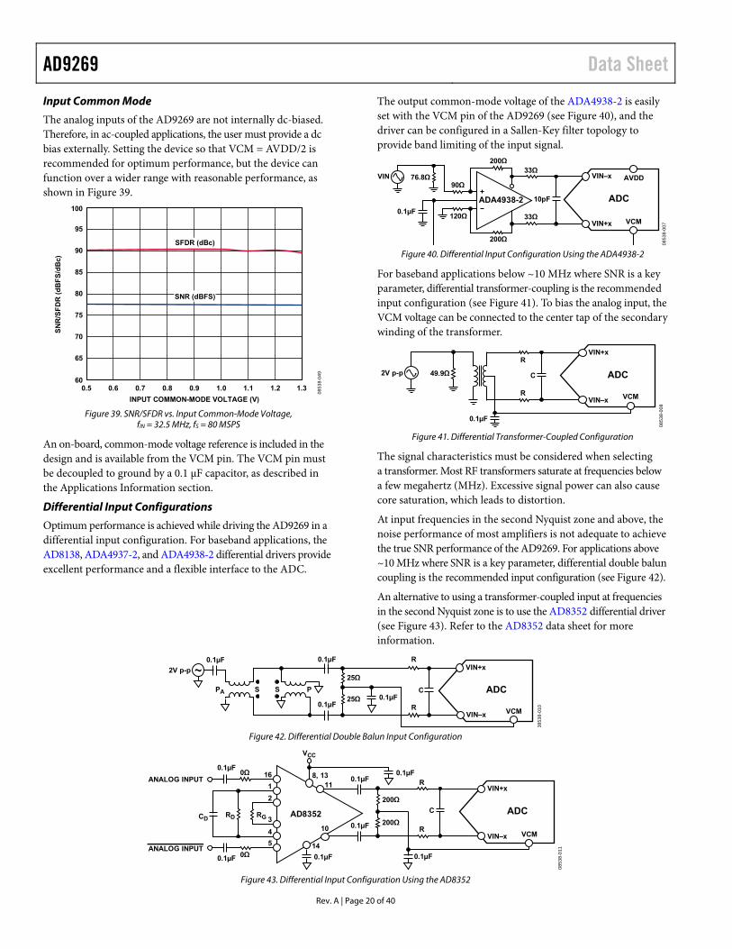
Optimum performance is achieved while driving the AD9269 in a differential input configuration. For baseband applications, the AD8138, ADA4937-2, and ADA4938-2 differential drivers provide excellent performance and a flexible interface to the ADC.
The output common-mode voltage of the ADA4938-2 is easily set with the VCM pin of the AD9269 (see Figure 40), and the driver can be configured in a Sallen-Key filter topology to provide band limiting of the input signal.
AVDDVIN 76.8Ω
120Ω0.1µF
33Ω
33Ω
10pF
200Ω
200Ω
90Ω
ADA4938-2 ADC
VIN–x
VIN+x VCM
0853
8-00
7
Figure 40. Differential Input Configuration Using the ADA4938-2
For baseband applications below ~10 MHz where SNR is a key parameter, differential transformer-coupling is the recommended input configuration (see Figure 41). To bias the analog input, the VCM voltage can be connected to the center tap of the secondary winding of the transformer.
2V p-p 49.9Ω
0.1µF
R
R
C ADC
VCM
VIN+x
VIN–x
0853
8-00
8
Figure 41. Differential Transformer-Coupled Configuration
The signal characteristics must be considered when selecting a transformer. Most RF transformers saturate at frequencies below a few megahertz (MHz). Excessive signal power can also cause core saturation, which leads to distortion.
At input frequencies in the second Nyquist zone and above, the noise performance of most amplifiers is not adequate to achieve the true SNR performance of the AD9269. For applications above ~10 MHz where SNR is a key parameter, differential double balun coupling is the recommended input configuration (see Figure 42).
An alternative to using a transformer-coupled input at frequencies in the second Nyquist zone is to use the AD8352 differential driver (see Figure 43). Refer to the AD8352 data sheet for more information.
ADC
R0.1µF0.1µF
2V p-p
VCM
C
R0.1µF
S0.1µF25Ω
25Ω
SPA P
0853
8-01
0
VIN+x
VIN–x
Figure 42. Differential Double Balun Input Configuration
AD8352
0Ω
0Ω
CDRD RG
0.1µF
0.1µF
0.1µF
0.1µF
16
1
2
3
4
5
11
0.1µF
0.1µF
10
14
0.1µF8, 13
VCC
200Ω
200Ω
ANALOG INPUT
ANALOG INPUT
R
R
C ADC
VCM
VIN+x
VIN–x
0853
8-01
1
Figure 43. Differential Input Configuration Using the AD8352
Data Sheet AD9269
Rev. A | Page 21 of 40
In any configuration, the value of Shunt Capacitor C is dependent on the input frequency and source impedance and may need to be reduced or removed. Table 9 displays the suggested values to set the RC network. However, these values are dependent on the input signal and should be used only as a starting guide.
Table 9. Example RC Network
Frequency Range (MHz) R Series (Ω Each) C Differential (pF)
0 to 70 33 22 70 to 200 125 Open
Single-Ended Input Configuration
A single-ended input can provide adequate performance in cost-sensitive applications. In this configuration, SFDR and distortion performance degrade due to the large input common-mode swing. If the source impedances on each input are matched, there should be little effect on SNR performance. Figure 44 shows a typical single-ended input configuration.
1V p-p
R
R
C
49.9Ω 0.1µF
10µF
10µF 0.1µF
AVDD
1kΩ
1kΩ
1kΩ
1kΩ
ADC
AVDD
VIN+x
VIN–x
0853
8-00
9
Figure 44. Single-Ended Input Configuration
VOLTAGE REFERENCE A stable and accurate 1.0 V voltage reference is built into the AD9269. VREF can be configured using either the internal 1.0 V reference or an externally applied 1.0 V reference voltage. The various reference modes are summarized in the sections that follow. The Reference Decoupling section describes the best-practices PCB layout of the reference.
Internal Reference Connection
A comparator within the AD9269 detects the potential at the SENSE pin and configures the reference into two possible modes, which are summarized in Table 10. If SENSE is grounded, the reference amplifier switch is connected to the internal resistor divider (see Figure 45), setting VREF to 1.0 V.
VREF
SENSE
0.5V
ADC
SELECTLOGIC
0.1µF1.0µF
VIN–A/VIN–B
VIN+A/VIN+B
ADCCORE
0853
8-01
2
Figure 45. Internal Reference Configuration
If the internal reference of the AD9269 drives multiple converters to improve gain matching, the loading of the reference by the other converters must be considered. Figure 46 shows how the internal reference voltage is affected by loading.
0
–3.00 2.0
LOAD CURRENT (mA)
REF
EREN
CE
VOLT
AG
E ER
RO
R (%
) –0.5
–1.0
–1.5
–2.0
–2.5
0.2 0.4 0.6 0.8 1.0 1.4 1.6 1.81.2
INTERNAL VREF = 0.993V
0853
8-01
4
Figure 46. VREF Accuracy vs. Load Current
Table 10. Reference Configuration Summary Selected Mode SENSE Voltage (V) Resulting VREF (V) Resulting Differential Span (V p-p) Fixed Internal Reference AGND to 0.2 1.0 internal 2.0 Fixed External Reference AVDD 1.0 applied to external VREF pin 2.0
AD9269 Data Sheet
Rev. A | Page 22 of 40
External Reference Operation
The use of an external reference may be necessary to enhance the gain accuracy of the ADC or to improve thermal drift characteristics. Figure 47 shows the typical drift characteristics of the internal reference in 1.0 V mode.
4
3
2
1
0
–1
–2
–3
–4
–5
–6–40 –20 0 20 40 60 80
TEMPERATURE (°C)
V REF
ER
RO
R (m
V)
VREF ERROR (mV)
0853
8-05
2
Figure 47. Typical VREF Drift
When the SENSE pin is tied to AVDD, the internal reference is disabled, allowing the use of an external reference. An internal reference buffer loads the external reference with an equivalent 7.5 kΩ load (see Figure 32). The internal buffer generates the positive and negative full-scale references for the ADC core. Therefore, the external reference must be limited to a maximum of 1.0 V.
CLOCK INPUT CONSIDERATIONS For optimum performance, clock the AD9269 sample clock inputs, CLK+ and CLK−, with a differential signal. The signal is typically ac-coupled into the CLK+ and CLK− pins via a transformer or capacitors. These pins are biased internally (see Figure 48) and require no external bias.
0.9V
AVDD
2pF 2pF
CLK–CLK+
0853
8-01
6
Figure 48. Equivalent Clock Input Circuit
Clock Input Options
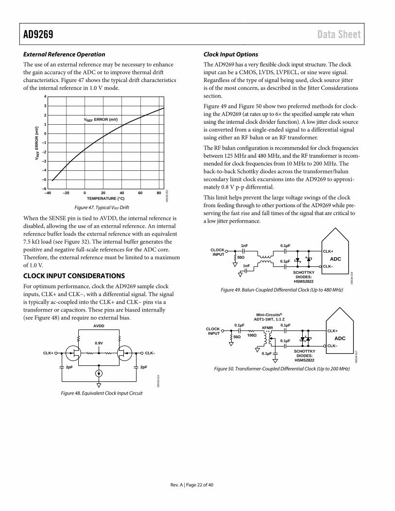
The AD9269 has a very flexible clock input structure. The clock input can be a CMOS, LVDS, LVPECL, or sine wave signal. Regardless of the type of signal being used, clock source jitter is of the most concern, as described in the Jitter Considerations section.
Figure 49 and Figure 50 show two preferred methods for clock-ing the AD9269 (at rates up to 6× the specified sample rate when using the internal clock divider function). A low jitter clock source is converted from a single-ended signal to a differential signal using either an RF balun or an RF transformer.
The RF balun configuration is recommended for clock frequencies between 125 MHz and 480 MHz, and the RF transformer is recom-mended for clock frequencies from 10 MHz to 200 MHz. The back-to-back Schottky diodes across the transformer/balun secondary limit clock excursions into the AD9269 to approxi-mately 0.8 V p-p differential.
This limit helps prevent the large voltage swings of the clock from feeding through to other portions of the AD9269 while pre-serving the fast rise and fall times of the signal that are critical to a low jitter performance.
0.1µF
0.1µF1nFCLOCKINPUT
1nF
50Ω
CLK–
CLK+
SCHOTTKYDIODES:
HSMS2822
ADC
0853
8-01
8
Figure 49. Balun-Coupled Differential Clock (Up to 480 MHz)
0.1µF
0.1µF
0.1µF0.1µF
SCHOTTKYDIODES:
HSMS2822
CLOCKINPUT
50Ω 100Ω
CLK–
CLK+
ADC
Mini-Circuits®ADT1-1WT, 1:1 Z
XFMR
0853
8-01
7
Figure 50. Transformer-Coupled Differential Clock (Up to 200 MHz)
Data Sheet AD9269
Rev. A | Page 23 of 40
If a low jitter clock source is not available, another option is to ac couple a differential PECL signal to the sample clock input pins, as shown in Figure 51. The AD9510/AD9511/AD9512/ AD9513/AD9514/AD9515/AD9516/AD9517 clock drivers offer excellent jitter performance.
100Ω
0.1µF
0.1µF0.1µF
0.1µF
240Ω240Ω50kΩ 50kΩ
CLK–
CLK+CLOCKINPUT
CLOCKINPUT
ADCAD951xPECL DRIVER
0853
8-01
9
Figure 51. Differential PECL Sample Clock (Up to 480 MHz)
A third option is to ac couple a differential LVDS signal to the sample clock input pins, as shown in Figure 52. The AD9510/ AD9511/AD9512/AD9513/AD9514/AD9515/AD9516/AD9517 clock drivers offer excellent jitter performance.
100Ω
0.1µF
0.1µF0.1µF
0.1µF
50kΩ 50kΩ
CLK–
CLK+
ADC
CLOCKINPUT
CLOCKINPUT
AD951xLVDS DRIVER
0853
8-02
0
Figure 52. Differential LVDS Sample Clock (Up to 480 MHz)
In some applications, it may be acceptable to drive the sample clock inputs with a single-ended 1.8 V CMOS signal. In such applications, drive the CLK+ pin directly from a CMOS gate, and bypass the CLK− pin to ground with a 0.1 μF capacitor (see Figure 53).
OPTIONAL100Ω 0.1µF
0.1µF
0.1µF
50Ω1
150Ω RESISTOR IS OPTIONAL.
CLK–
CLK+
ADC
VCC
1kΩ
1kΩ
CLOCKINPUT
AD951xCMOS DRIVER
0853
8-02
1
Figure 53. Single-Ended 1.8 V CMOS Input Clock (Up to 200 MHz)
Input Clock Divider
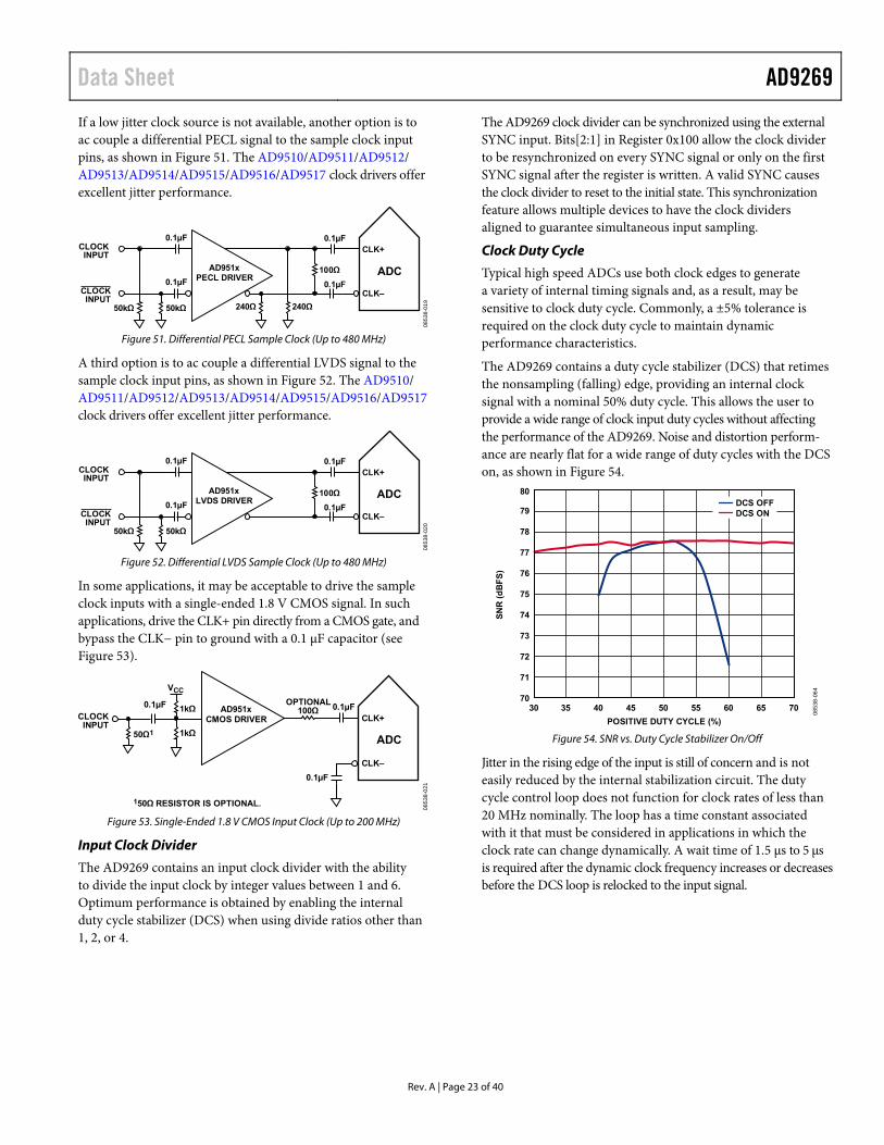
The AD9269 contains an input clock divider with the ability to divide the input clock by integer values between 1 and 6. Optimum performance is obtained by enabling the internal duty cycle stabilizer (DCS) when using divide ratios other than 1, 2, or 4.
The AD9269 clock divider can be synchronized using the external SYNC input. Bits[2:1] in Register 0x100 allow the clock divider to be resynchronized on every SYNC signal or only on the first SYNC signal after the register is written. A valid SYNC causes the clock divider to reset to the initial state. This synchronization feature allows multiple devices to have the clock dividers aligned to guarantee simultaneous input sampling.
Clock Duty Cycle
Typical high speed ADCs use both clock edges to generate a variety of internal timing signals and, as a result, may be sensitive to clock duty cycle. Commonly, a ±5% tolerance is required on the clock duty cycle to maintain dynamic performance characteristics.
The AD9269 contains a duty cycle stabilizer (DCS) that retimes the nonsampling (falling) edge, providing an internal clock signal with a nominal 50% duty cycle. This allows the user to provide a wide range of clock input duty cycles without affecting the performance of the AD9269. Noise and distortion perform-ance are nearly flat for a wide range of duty cycles with the DCS on, as shown in Figure 54.
80
79
78
77
76
70
71
72
73
74
75
30 35 40 45 50 55 60 65 70
SN
R (
dB
FS
)
POSITIVE DUTY CYCLE (%)
0853
8-06
4
DCS OFFDCS ON
Figure 54. SNR vs. Duty Cycle Stabilizer On/Off
Jitter in the rising edge of the input is still of concern and is not easily reduced by the internal stabilization circuit. The duty cycle control loop does not function for clock rates of less than 20 MHz nominally. The loop has a time constant associated with it that must be considered in applications in which the clock rate can change dynamically. A wait time of 1.5 μs to 5 μs is required after the dynamic clock frequency increases or decreases before the DCS loop is relocked to the input signal.

AD9269 Data Sheet
Rev. A | Page 24 of 40
Jitter Considerations
High speed, high resolution ADCs are sensitive to the quality of the clock input. The degradation in SNR from the low fre-quency SNR (SNRLF) at a given input frequency (fINPUT) due to jitter (tJRMS) can be calculated by
SNRHF = −10 log[(2π × fINPUT × tJRMS)2 + 10 )10/( LFSNR− ]
In the previous equation, the rms aperture jitter represents the clock input jitter specification. IF undersampling applications are particularly sensitive to jitter, as illustrated in Figure 55.
80
75
70
65
60
55
50
451 10 100 1k
FREQUENCY (MHz)
SNR
(dB
FS)
0793
8-02
2
0.5ps
0.2ps
0.05ps
1.0ps
1.5ps2.0ps2.5ps3.0ps
Figure 55. SNR vs. Input Frequency and Jitter
The clock input should be treated as an analog signal in cases in which aperture jitter may affect the dynamic range of the AD9269. To avoid modulating the clock signal with digital noise, keep power supplies for clock drivers separate from the ADC output driver supplies. Low jitter, crystal-controlled oscillators make the best clock sources. If the clock is generated from another type of source (by gating, dividing, or another method), it should be retimed by the original clock at the last step.
For more information, see the AN-501 Application Note and the AN-756 Application Note, available on www.analog.com.
POWER DISSIPATION AND STANDBY MODE As shown in Figure 56, the analog core power dissipated by the AD9269 is proportional to the sample rate. The digital power dis-sipation of the CMOS outputs is determined primarily by the strength of the digital drivers and the load on each output bit.
The maximum DRVDD current (IDRVDD) can be calculated as
IDRVDD = VDRVDD × CLOAD × fCLK × N
where N is the number of output bits (34, in the case of the AD9269).
210
70
90
110
130
150
170
190
10 20 30 40 50 60 70 80
AN
ALO
G C
OR
E PO
WER
(mW
)
CLOCK RATE (MSPS)
0853
8-05
1
AD9269-80
AD9269-65
AD9269-40
AD9269-20
Figure 56. Analog Core Power vs. Clock Rate
This maximum current occurs when every output bit switches on every clock cycle, that is, a full-scale square wave at the Nyquist frequency of fCLK/2. In practice, the DRVDD current is estab-lished by the average number of output bits switching, which is determined by the sample rate and the characteristics of the analog input signal.
Reducing the capacitive load presented to the output drivers can minimize digital power consumption. The data in Figure 56 was taken using the same operating conditions as those used for the Typical Performance Characteristics, with a 5 pF load on each output driver.
Data Sheet AD9269
Rev. A | Page 25 of 40
The AD9269 is placed in power-down mode either by the SPI port or by asserting the PDWN pin high. In this state, the ADC typically dissipates 1 mW. During power-down, the output drivers are placed in a high impedance state. Asserting the PDWN pin low returns the AD9269 to the normal operating mode. Note that PDWN is referenced to the digital output driver supply (DRVDD) and should not exceed that supply voltage.
Low power dissipation in power-down mode is achieved by shutting down the reference, reference buffer, biasing networks, and clock. Internal capacitors are discharged when entering power-down mode and then must be recharged when returning to normal operation. As a result, wake-up time is related to the time spent in power-down mode, and shorter power-down cycles result in proportionally shorter wake-up times.
When using the SPI port interface, the user can place the ADC in power-down mode or standby mode. Standby mode allows the user to keep the internal reference circuitry powered when faster wake-up times are required. See the Memory Map section for more details.
DIGITAL OUTPUTS The AD9269 output drivers can be configured to interface with 1.8 V to 3.3 V CMOS logic families. Output data can also be multi-plexed onto a single output bus to reduce the total number of traces required.
The CMOS output drivers are sized to provide sufficient output current to drive a wide variety of logic families. However, large drive currents tend to cause current glitches on the supplies and may affect converter performance.
Applications requiring the ADC to drive large capacitive loads or large fanouts may require external buffers or latches.
The output data format can be selected to be either offset binary or twos complement by setting the SCLK/DFS pin when operating in the external pin mode (see Table 11).
Table 11. SCLK/DFS Mode Selection (External Pin Mode) Voltage at Pin SCLK/DFS SDIO/DCS AGND Offset binary (default) DCS disabled DRVDD Twos complement DCS enabled (default)
As detailed in the AN-877 Application Note, Interfacing to High Speed ADCs via SPI, the data format can be selected for offset binary, twos complement, or gray code when using the SPI control.
Digital Output Enable Function (OEB)
The AD9269 provides a flexible three-state ability for the digital output pins. The three-state mode is enabled by the OEB pin or through the SPI interface. If the OEB pin is low, the output data drivers and DCOs are enabled. If the OEB pin is high, the output data drivers and DCOs are placed in a high impedance state. This OEB function is not intended for rapid access to the data bus. Note that OEB is referenced to the digital output driver supply (DRVDD) and should not exceed that supply voltage.
When using the SPI interface, the data outputs and DCO of each channel can be independently three-stated by using the output disable (OEB) bit, Bit 4 in Register 0x14.
TIMING The AD9269 provides latched data with a pipeline delay of nine clock cycles. Data outputs are available one propagation delay (tPD) after the rising edge of the clock signal.
Minimize the length of the output data lines and loads placed on them to reduce transients within the AD9269. These transients may degrade converter dynamic performance.
The lowest typical conversion rate of the AD9269 is 3 MSPS. At clock rates below 3 MSPS, dynamic performance may degrade.
Data Clock Output (DCO)
The AD9269 provides two data clock output (DCO) signals that are designed to capture the data in an external register. The CMOS data outputs are valid on the rising edge of DCO unless the DCO clock polarity has been changed via the SPI. See Figure 2 and Figure 3 for a graphical timing description.
Table 12. Output Data Format Input (V) Condition (V) Offset Binary Output Mode Twos Complement Mode OR VIN+ − VIN− < −VREF − 0.5 LSB 0000 0000 0000 0000 1000 0000 0000 0000 1 VIN+ − VIN− = −VREF 0000 0000 0000 0000 1000 0000 0000 0000 0 VIN+ − VIN− = 0 1000 0000 0000 0000 0000 0000 0000 0000 0 VIN+ − VIN− = +VREF − 1.0 LSB 1111 1111 1111 1111 0111 1111 1111 1111 0 VIN+ − VIN− > +VREF − 0.5 LSB 1111 1111 1111 1111 0111 1111 1111 1111 1

AD9269 Data Sheet
Rev. A | Page 26 of 40
BUILT-IN SELF-TEST (BIST) AND OUTPUT TEST The AD9269 includes a built-in test feature that is designed to enable verification of the integrity of each channel as well as to facilitate board-level debugging. A built-in self-test (BIST) feature that verifies the integrity of the digital datapath of the AD9269 is included. Various output test options are also provided to place predictable values on the outputs of the AD9269.
BUILT-IN SELF-TEST (BIST) The BIST is a thorough test of the digital portion of the selected AD9269 signal path. Perform the BIST test after a reset to ensure that the device is in a known state. During BIST, data from an internal pseudorandom noise (PN) source is driven through the digital datapath of both channels, starting at the ADC block output. At the datapath output, CRC logic calculates a signature from the data. The BIST sequence runs for 512 cycles and then stops. When the sequence is complete, the BIST compares the signature results with a predetermined value. If the signatures match, the BIST sets Bit 0 in Register 0x24, signifying that the test passed. If the BIST test failed, Bit 0 in Register 0x24 is cleared. The outputs are connected during this test, so the PN sequence can be observed as it runs.
Writing the value 0x05 to Register 0x0E runs the BIST. This enables Bit 0 (BIST enable) in Register 0x0E and resets the PN sequence generator, Bit 2 (BIST init) in Register 0x0E. At the completion of the BIST, Bit 0 in Register 0x24 is automatically cleared. The PN sequence can be continued from the last value by writing a 0 in Bit 2 in Register 0x0E. However, if the PN sequence is not reset, the signature calculation does not equal the predetermined value at the end of the test. At that point, the user must rely on verifying the output data.
OUTPUT TEST MODES The output test options are described in Table 17 at Address 0x0D. When an output test mode is enabled, the analog section of the ADC is disconnected from the digital back end blocks, and the test pattern is run through the output formatting block. Some of the test patterns are subject to output formatting, and some are not. The PN generators from the PN sequence tests can be reset by setting Bit 4 or Bit 5 in Register 0x0D. These tests can be per-formed with or without an analog signal (if present, the analog signal is ignored), but they do require an encode clock. For more information, see the AN-877 Application Note, Interfacing to High Speed ADCs via SPI.

Data Sheet AD9269
Rev. A | Page 27 of 40
CHANNEL/CHIP SYNCHRONIZATION The AD9269 has a SYNC input that offers the user flexible synchronization options for synchronizing sample clocks across multiple ADCs. The input clock divider can be enabled to synchronize on a single occurrence of the SYNC signal or on every occurrence.
The SYNC input is internally synchronized to the sample clock; however, to ensure that there is no timing uncertainty between multiple devices, the SYNC input signal should be externally synchronized to the input clock signal, meeting the setup and hold times that are shown in Table 5. Drive the SYNC input using a single-ended CMOS-type signal.

AD9269 Data Sheet
Rev. A | Page 28 of 40
DC AND QUADRATURE ERROR CORRECTION (QEC) In direct conversion or other quadrature systems, mismatches between the real (I) and imaginary (Q) signal paths cause fre-quencies in the positive spectrum to image into the negative spectrum, and vice versa. From an RF point of view, this is equivalent to information above the local oscillator (LO) frequency interfering with information below the LO frequency, and vice versa. These mismatches may occur from gain and/or phase mismatches in the analog quadrature demodulator or in any other mismatches between the I and Q signal chains. In a single-carrier zero-IF system where the carrier has been placed symmetrically around dc, this causes self-distortion of the carrier as the two sidebands fold onto one another and degrade the error vector magnitude (EVM) of the signal.
In a multicarrier communication system, this can be even more problematic because carriers of widely different power levels can interfere with one another. For example, a large carrier centered at +f1 can have an image appear at −f1 that may be much larger than the desired carrier at −f1.
The integrated quadrature error correction (QEC) algorithm of the AD9269 attempts to measure and correct the amplitude and phase imbalances of the I and Q signal paths to achieve higher levels of image suppression than is achievable by analog means alone. These errors can be corrected in an adapted manner, in which the I and Q gain and quadrature phase mismatches are constantly estimated and corrected, allowing for constant tracking of slow changes in mismatches that are due to supply and temperature.
The quadrature errors are corrected in a frequency independent manner on the AD9269; therefore, systems with significant mismatch in the baseband I and Q signal chains may have reduced image suppression. The AD9269 QEC still corrects the systematic imbalances.
The convergence time of the QEC algorithm is dependent on the statistics of the input signal. For large signals and large imbalance errors, this convergence time is typically less than 2 million samples of the AD9269 data rate.
LO Leakage (DC) Correction
In a direct conversion receiver subsystem, LO to RF leakage of the quadrature modulator shows up as dc offsets at baseband. These offsets are added to dc offsets in the baseband signal paths, and both contribute to a carrier at dc. In a zero-IF receiver, this dc energy can cause problems because it appears in band of a desired channel. As part of the QEC function, the dc offset is suppressed by applying a low frequency notch filter to form a null around dc.
In applications where constant tracking of the dc offsets and quadrature errors are not needed, the algorithms can be independently frozen to save power. When frozen, the image and LO leakage (dc) correction are still performed, but changes are no longer tracked. Bits[5:3] in Register 0x110 disable the respective correction when frozen.
The default configuration on the AD9269 has the QEC and dc correction blocks disabled, and Bits[2:0] in Register 0x110 must be pulled high to enable the correction blocks. The quadrature gain, quadrature phase, and dc correction algorithms can also be disabled independently for system debugging or to save power by pulling Bits[2:0] low in Register 0x110.
When the QEC is enabled and a correction value has been calculated, the value remains active as long as any of the QEC functions (DC, gain, or phase correction) are being used.
QEC and DC Correction Range
Table 13 gives the minimum and maximum correction ranges of the algorithms. If the mismatches are greater than these ranges, an imperfect correction results.
Table 13. QEC and DC Correction Range Parameter Minimum Maximum Gain −1.1 dB +1.0 dB Phase −1.79 degrees +1.79 degrees DC −6 % +6%
0
–15
–30
–45
–60
–75
–135
–120
–105
–90
–30.
0M
–37.
5M
–22.
5M
–15.
0M
–7.5
M 0M
7.5M 15M
22.5
M
30M
37.5
M
AM
PLIT
UD
E (d
BFS
)
FREQUENCY (MHz) 0853
8-06
5
43
25
6
IMAGEDC OFFSET
Figure 57. QEC Mode Off
0
–15
–30
–45
–60
–75
–135
–120
–105
–90
–30.
0M
–37.
5M
–22.
5M
–15.
0M
–7.5
M 0M
7.5M 15M
22.5
M
30M
37.5
M
AM
PLIT
UD
E (d
BFS
)
FREQUENCY (MHz) 0853
8-06
6
43
256
IMAGEDC OFFSET
Figure 58. QEC Mode On
Data Sheet AD9269
Rev. 0 | Page 29 of 40
SERIAL PORT INTERFACE (SPI) The AD9269 serial port interface (SPI) allows the user to configure the converter for specific functions or operations through a struc-tured register space provided inside the ADC. The SPI provides added flexibility and customization, depending on the application. Addresses are accessed via the serial port and can be written to or read from via the port. Memory is organized into bytes that can be further divided into fields, which are documented in the Memory Map section. For detailed operational information, see the AN-877 Application Note, Interfacing to High Speed ADCs via SPI.
CONFIGURATION USING THE SPI Three pins define the SPI of this ADC: the SCLK, the SDIO, and the CSB (see Table 14). The SCLK (a serial clock) synchronizes the read and write data presented from and to the ADC. The SDIO (serial data input/output) is a dual-purpose pin that allows data to be sent to and read from the internal ADC memory map registers. The CSB (chip select bar) is an active-low control that enables or disables the read and write cycles.
Table 14. Serial Port Interface Pins Pin Function SCLK Serial clock. A serial shift clock input that synchronizes
serial interface reads and writes. SDIO Serial data input/output. A dual-purpose pin that
typically serves as an input or an output, depending on the instruction being sent and the relative position in the timing frame.
CSB Chip select bar. An active-low control that gates the read and write cycles.
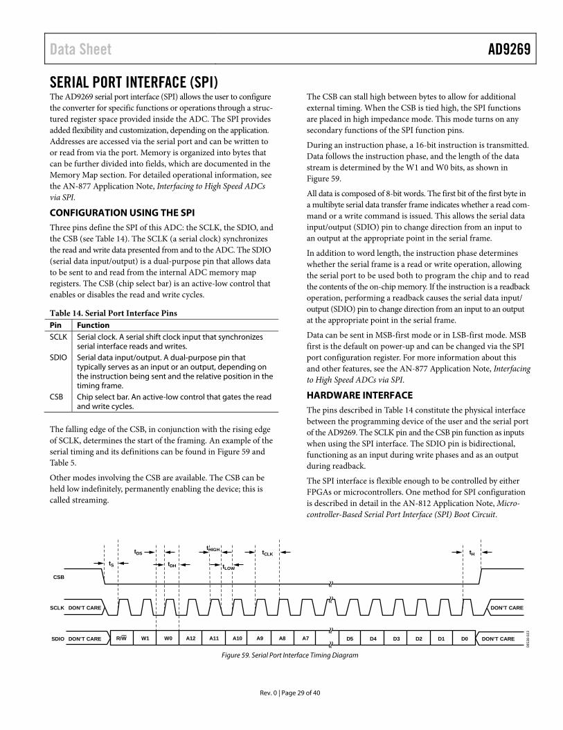
The falling edge of the CSB, in conjunction with the rising edge of SCLK, determines the start of the framing. An example of the serial timing and its definitions can be found in Figure 59 and Table 5.
Other modes involving the CSB are available. The CSB can be held low indefinitely, permanently enabling the device; this is called streaming.
The CSB can stall high between bytes to allow for additional external timing. When the CSB is tied high, the SPI functions are placed in high impedance mode. This mode turns on any secondary functions of the SPI function pins.
During an instruction phase, a 16-bit instruction is transmitted. Data follows the instruction phase, and the length of the data stream is determined by the W1 and W0 bits, as shown in Figure 59.
All data is composed of 8-bit words. The first bit of the first byte in a multibyte serial data transfer frame indicates whether a read com-mand or a write command is issued. This allows the serial data input/output (SDIO) pin to change direction from an input to an output at the appropriate point in the serial frame.
In addition to word length, the instruction phase determines whether the serial frame is a read or write operation, allowing the serial port to be used both to program the chip and to read the contents of the on-chip memory. If the instruction is a readback operation, performing a readback causes the serial data input/ output (SDIO) pin to change direction from an input to an output at the appropriate point in the serial frame.
Data can be sent in MSB-first mode or in LSB-first mode. MSB first is the default on power-up and can be changed via the SPI port configuration register. For more information about this and other features, see the AN-877 Application Note, Interfacing to High Speed ADCs via SPI.
HARDWARE INTERFACE The pins described in Table 14 constitute the physical interface between the programming device of the user and the serial port of the AD9269. The SCLK pin and the CSB pin function as inputs when using the SPI interface. The SDIO pin is bidirectional, functioning as an input during write phases and as an output during readback.
The SPI interface is flexible enough to be controlled by either FPGAs or microcontrollers. One method for SPI configuration is described in detail in the AN-812 Application Note, Micro-controller-Based Serial Port Interface (SPI) Boot Circuit.
DON’T CARE
DON’T CAREDON’T CARE
DON’T CARE
SDIO
SCLK
CSB
tS tDH
tCLKtDS tH
R/W W1 W0 A12 A11 A10 A9 A8 A7 D5 D4 D3 D2 D1 D0
tLOW
tHIGH
0853
8-02
3
Figure 59. Serial Port Interface Timing Diagram
AD9269 Data Sheet
Rev. A | Page 30 of 40
The SPI port should not be active during periods when the full dynamic performance of the converter is required. Because the SCLK signal, the CSB signal, and the SDIO signal are typically asynchronous to the ADC clock, noise from these signals can degrade converter performance. If the on-board SPI bus is used for other devices, it may be necessary to provide buffers between this bus and the AD9269 to prevent these signals from transitioning at the converter inputs during critical sampling periods.
SDIO/DCS and SCLK/DFS serve a dual function when the SPI interface is not being used. When the pins are strapped to DRVDD or ground during device power-on, they are associated with a specific function. The Digital Outputs section describes the strappable functions supported on the AD9269.
CONFIGURATION WITHOUT THE SPI In applications that do not interface to the SPI control registers, the SDIO/DCS pin, the SCLK/DFS pin, the OEB pin, and the PDWN pin serve as standalone CMOS-compatible control pins. When the device is powered up, it is assumed that the user intends to use the pins as static control lines for the duty cycle stabilizer, output data format, output enable, and power-down feature con-trol. In this mode, connect the CSB chip select to DRVDD, which disables the serial port interface.
Table 15. Mode Selection
Pin External Voltage Configuration
SDIO/DCS DRVDD (default) Duty cycle stabilizer enabled AGND Duty cycle stabilizer disabled
SCLK/DFS DRVDD Twos complement enabled AGND (default) Offset binary enabled
OEB DRVDD Outputs in high impedance AGND (default) Outputs enabled
PDWN DRVDD Chip in power-down or standby AGND (default) Normal operation
SPI ACCESSIBLE FEATURES Table 16 provides a brief description of the general features that are accessible via the SPI. These features are described in detail in the AN-877 Application Note, Interfacing to High Speed ADCs via SPI. The AD9269 device specific features are described in detail in Table 17.
Table 16. Features Accessible Using the SPI Feature Description Mode Allows the user to set either power-down mode
or standby mode Clock Allows the user to access the DCS via the SPI Offset Allows the user to digitally adjust the
converter offset Test I/O Allows the user to set test modes to have known
data on output bits Output Mode Allows the user to set up outputs Output Phase Allows the user to set the output clock polarity Output Delay Allows the user to vary the DCO delay VREF Allows the user to set the reference voltage
Data Sheet AD9269
Rev. A | Page 31 of 40
MEMORY MAP READING THE MEMORY MAP REGISTER TABLE Each row in the memory map register table (see Table 17) contains eight bit locations. The memory map is divided into four sections: the chip configuration registers (Address 0x00 to Address 0x02); the device index and transfer registers (Address 0x05 and Address 0xFF); the program registers, including setup, control, and test (Address 0x08 to Address 0x2E); and the digital feature control registers (Address 0x100 to Address 0x11D).
Table 17 documents the default hexadecimal value for each hexadecimal address shown. The column with the heading Bit 7 (MSB) is the start of the default hexadecimal value given. For example, Address 0x05, the channel index register, has a hexa-decimal default value of 0x03. This means that in Address 0x05, Bits[7:2] = 0, and the remaining Bits[1:0] = 1. This setting is the default channel index setting. The default value results in both ADC channels receiving the next write command. For more information on this function and others, see the AN-877 Application Note, Interfacing to High Speed ADCs via SPI. This document details the functions controlled by Register 0x00 to Register 0xFF. The remaining registers, Register 0x100 to Register 0x11D, are documented in the Memory Map Register Descriptions section following Table 17.
OPEN LOCATIONS All address and bit locations that are not included in the SPI map are not currently supported for this device. Unused bits of a valid address location should be written with 0s. Writing to these locations is required only when part of an address location is open (for example, Address 0x05). If the entire address location is open, it is omitted from the SPI map (for example, Address 0x13) and should not be written.
DEFAULT VALUES After the AD9269 is reset, critical registers are loaded with default values. The default values for the registers are given in the memory map register table (see Table 17).
Logic Levels
An explanation of logic level terminology follows:
• “Bit is set” is synonymous with “bit is set to Logic 1” or “writing Logic 1 for the bit.”
• “Clear a bit” is synonymous with “bit is set to Logic 0” or “writing Logic 0 for the bit.”
Transfer Register Map
Address 0x08 to Address 0x18 are shadowed. Writes to these addresses do not affect device operation until a transfer command is issued by writing 0x01 to Address 0xFF, setting the transfer bit. This allows these registers to be updated internally and simulta-neously when the transfer bit is set. The internal update takes place when the transfer bit is set, and then the bit autoclears.
Channel-Specific Registers
Some channel setup functions can be programmed differently for each channel. In these cases, channel address locations are internally duplicated for each channel. These registers and bits are designated in the memory map register table as local. These local registers and bits can be accessed by setting the appropriate Channel A (Bit 0) or Channel B (Bit 1) bits in Register 0x05.
If both bits are set, the subsequent write affects the registers of both channels. In a read cycle, set only Channel A or Channel B to read one of the two registers. If both bits are set during an SPI read cycle, the device returns the value for Channel A. Registers and bits designated as global in the memory map register table affect the entire device or the channel features for which independent settings are not allowed between channels. The settings in Register 0x05 do not affect the global registers and bits.
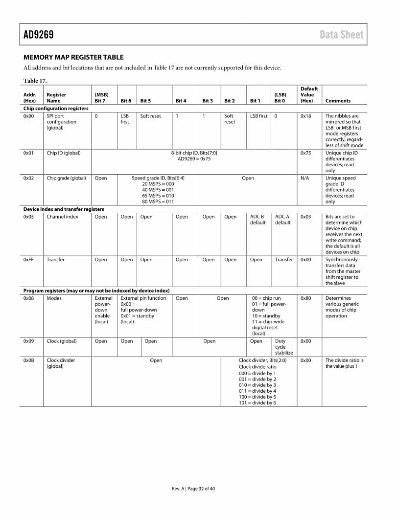
AD9269 Data Sheet
Rev. A | Page 32 of 40
MEMORY MAP REGISTER TABLE All address and bit locations that are not included in Table 17 are not currently supported for this device.
Table 17.
Addr. (Hex)
Register Name
(MSB) Bit 7 Bit 6 Bit 5 Bit 4 Bit 3 Bit 2 Bit 1
(LSB) Bit 0
Default Value (Hex) Comments
Chip configuration registers
0x00 SPI port configuration (global)
0 LSB first
Soft reset 1 1 Soft reset
LSB first 0 0x18 The nibbles are mirrored so that LSB- or MSB-first mode registers correctly, regard-less of shift mode
0x01 Chip ID (global) 8-bit chip ID, Bits[7:0] AD9269 = 0x75
0x75 Unique chip ID differentiates devices; read only
0x02 Chip grade (global) Open Speed grade ID, Bits[6:4] 20 MSPS = 000 40 MSPS = 001 65 MSPS = 010 80 MSPS = 011
Open N/A Unique speed grade ID differentiates devices; read only
Device index and transfer registers 0x05 Channel index Open Open Open Open Open Open ADC B
default ADC A default
0x03 Bits are set to determine which device on chip receives the next write command; the default is all devices on chip
0xFF Transfer Open Open Open Open Open Open Open Transfer 0x00 Synchronously transfers data from the master shift register to the slave
Program registers (may or may not be indexed by device index) 0x08 Modes External
power-down enable (local)
External pin function 0x00 = full power-down 0x01 = standby (local)
Open Open 00 = chip run 01 = full power-down 10 = standby 11 = chip-wide digital reset (local)
0x80 Determines various generic modes of chip operation
0x09 Clock (global) Open Open Open Open Open Duty cycle stabilize
0x00
0x0B Clock divider (global)
Open Clock divider, Bits[2:0] Clock divide ratio 000 = divide by 1 001 = divide by 2 010 = divide by 3 011 = divide by 4 100 = divide by 5 101 = divide by 6
0x00 The divide ratio is the value plus 1
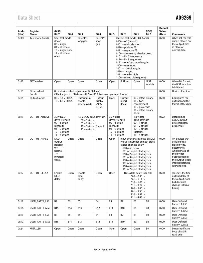
Data Sheet AD9269
Rev. A | Page 33 of 40
Addr. (Hex)
Register Name
(MSB) Bit 7 Bit 6 Bit 5 Bit 4 Bit 3 Bit 2 Bit 1
(LSB) Bit 0
Default Value (Hex) Comments
0x0D Test mode (local) User test mode (local) 00 = single 01 = alternate 10 = single once 11 = alternate once
Reset PN long gen
Reset PN short gen
Output test mode [3:0] (local) 0000 = off (default) 0001 = midscale short 0010 = positive FS 0011 = negative FS 0100 = alternating checkerboard 0101 = PN 23 sequence 0110 = PN 9 sequence 0111 = one/zero word toggle 1000 = user input 1001 = 1-/0-bit toggle 1010 = 1× sync 1011 = one bit high 1100 = mixed bit frequency
0x00 When set, the test data is placed on the output pins in place of normal data
0x0E BIST enable Open Open Open Open Open BIST init Open BIST enable
0x00 When Bit 0 is set, the BIST function is initiated
0x10 Offset adjust (local)
8-bit device offset adjustment [7:0] (local) Offset adjust in LSBs from +127 to −128 (twos complement format)
0x00 Device offset trim
0x14 Output mode 00 = 3.3 V CMOS 10 = 1.8 V CMOS
Output mux enable (interleaved)
Output disable (OEB) (local)
Open Output invert (local)
00 = offset binary 01 = twos complement 10 = gray code 11 = offset binary (local)
0x00 Configures the outputs and the format of the data
0x15 OUTPUT_ADJUST 3.3 V DCO drive strength 00 = 1 stripe (default) 01 = 2 stripes 10 = 3 stripes 11 = 4 stripes
1.8 V DCO drive strength 00 = 1 stripe 01 = 2 stripes 10 = 3 stripes (default) 11 = 4 stripes
3.3 V data drive strength 00 = 1 stripe (default) 01 = 2 stripes 10 = 3 stripes 11 = 4 stripes
1.8 V data drive strength 00 = 1 stripe 01 = 2 stripes 10 = 3 stripes (default) 11 = 4 stripes
0x22 Determines CMOS output drive strength properties
0x16 OUTPUT_PHASE DCO output polarity 0 = normal 1 = inverted (local)
Open Open Open Open Input clock phase adjust, Bits[2:0] (Value is number of input clock cycles of phase delay)
000 = no delay 001 = 1 input clock cycle 010 = 2 input clock cycles 011 = 3 input clock cycles 100 = 4 input clock cycles 101 = 5 input clock cycles 110 = 6 input clock cycles 111 = 7 input clock cycles
0x00 On devices that utilize global clock divide, determines which phase of the divider output supplies the output clock; internal latching is unaffected
0x17 OUTPUT_DELAY Enable DCO delay
Open Enable data delay
Open Open DCO/data delay, Bits[2:0] 000 = 0.56 ns 001 = 1.12 ns 010 = 1.68 ns 011 = 2.24 ns 100 = 2.80 ns 101 = 3.36 ns 110 = 3.92 ns 111 = 4.48 ns
0x00 This sets the fine output delay of the output clock but does not change internal timing
0x19 USER_PATT1_LSB B7 B6 B5 B4 B3 B2 B1 B0 0x00 User-Defined Pattern 1, LSB
0x1A USER_PATT1_MSB B15 B14 B13 B12 B11 B10 B9 B8 0x00 User-Defined Pattern 1, MSB
0x1B USER_PATT2_LSB B7 B6 B5 B4 B3 B2 B1 B0 0x00 User-Defined Pattern 2, LSB
0x1C USER_PATT2_MSB B15 B14 B13 B12 B11 B10 B9 B8 0x00 User-Defined Pattern 2, MSB
0x24 MISR_LSB Open Open Open Open Open Open Open B0 0x00 Least significant byte of MISR; read only
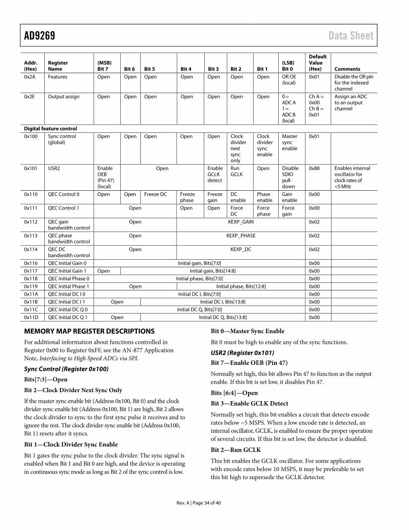
AD9269 Data Sheet
Rev. A | Page 34 of 40
Addr. (Hex)
Register Name
(MSB) Bit 7 Bit 6 Bit 5 Bit 4 Bit 3 Bit 2 Bit 1
(LSB) Bit 0
Default Value (Hex) Comments
0x2A Features Open Open Open Open Open Open Open OR OE (local)
0x01 Disable the OR pin for the indexed channel
0x2E Output assign Open Open Open Open Open Open Open 0 = ADC A 1 = ADC B (local)
Ch A = 0x00 Ch B = 0x01
Assign an ADC to an output channel
Digital feature control 0x100 Sync control
(global) Open Open Open Open Open Clock
divider next sync only
Clock divider sync enable
Master sync enable
0x01
0x101 USR2 Enable OEB (Pin 47) (local)
Open Enable GCLK detect
Run GCLK
Open Disable SDIO pull-down
0x88 Enables internal oscillator for clock rates of <5 MHz
0x110 QEC Control 0 Open Open Freeze DC Freeze phase
Freeze gain
DC enable
Phase enable
Gain enable
0x00
0x111 QEC Control 1 Open Open Open Force DC
Force phase
Force gain
0x00
0x112 QEC gain bandwidth control
Open KEXP_GAIN 0x02
0x113 QEC phase bandwidth control
Open KEXP_PHASE 0x02
0x114 QEC DC bandwidth control
Open KEXP_DC 0x02
0x116 QEC Initial Gain 0 Initial gain, Bits[7:0] 0x00
0x117 QEC Initial Gain 1 Open Initial gain, Bits[14:8] 0x00
0x118 QEC Initial Phase 0 Initial phase, Bits[7:0] 0x00
0x119 QEC Initial Phase 1 Open Initial phase, Bits[12:8] 0x00
0x11A QEC Initial DC I 0 Initial DC I, Bits[7:0] 0x00
0x11B QEC Initial DC I 1 Open Initial DC I, Bits[13:8] 0x00
0x11C QEC Initial DC Q 0 Initial DC Q, Bits[7:0] 0x00
0x11D QEC Initial DC Q 1 Open Initial DC Q, Bits[13:8] 0x00
MEMORY MAP REGISTER DESCRIPTIONS For additional information about functions controlled in Register 0x00 to Register 0xFF, see the AN-877 Application Note, Interfacing to High Speed ADCs via SPI.
Sync Control (Register 0x100)
Bits[7:3]—Open
Bit 2—Clock Divider Next Sync Only
If the master sync enable bit (Address 0x100, Bit 0) and the clock divider sync enable bit (Address 0x100, Bit 1) are high, Bit 2 allows the clock divider to sync to the first sync pulse it receives and to ignore the rest. The clock divider sync enable bit (Address 0x100, Bit 1) resets after it syncs.
Bit 1—Clock Divider Sync Enable
Bit 1 gates the sync pulse to the clock divider. The sync signal is enabled when Bit 1 and Bit 0 are high, and the device is operating in continuous sync mode as long as Bit 2 of the sync control is low.
Bit 0—Master Sync Enable
Bit 0 must be high to enable any of the sync functions.
USR2 (Register 0x101)
Bit 7—Enable OEB (Pin 47)
Normally set high, this bit allows Pin 47 to function as the output enable. If this bit is set low, it disables Pin 47.
Bits [6:4]—Open Bit 3—Enable GCLK Detect
Normally set high, this bit enables a circuit that detects encode rates below ~5 MSPS. When a low encode rate is detected, an internal oscillator, GCLK, is enabled to ensure the proper operation of several circuits. If this bit is set low, the detector is disabled.
Bit 2—Run GCLK
This bit enables the GCLK oscillator. For some applications with encode rates below 10 MSPS, it may be preferable to set this bit high to supersede the GCLK detector.
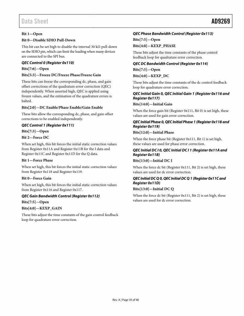
Data Sheet AD9269
Rev. A | Page 35 of 40
Bit 1—Open Bit 0—Disable SDIO Pull-Down
This bit can be set high to disable the internal 30 kΩ pull-down on the SDIO pin, which can limit the loading when many devices are connected to the SPI bus.
QEC Control 0 (Register 0x110)
Bits[7:6]—Open Bits[5:3]—Freeze DC/Freeze Phase/Freeze Gain
These bits can freeze the corresponding dc, phase, and gain offset corrections of the quadrature error correction (QEC) independently. When asserted high, QEC is applied using frozen values, and the estimation of the quadrature errors is halted.
Bits[2:0]—DC Enable/Phase Enable/Gain Enable
These bits allow the corresponding dc, phase, and gain offset corrections to be enabled independently.
QEC Control 1 (Register 0x111)
Bits[7:3]—Open Bit 2—Force DC
When set high, this bit forces the initial static correction values from Register 0x11A and Register 0x11B for the I data and Register 0x11C and Register 0x11D for the Q data.
Bit 1—Force Phase
When set high, this bit forces the initial static correction values from Register 0x118 and Register 0x119.
Bit 0—Force Gain
When set high, this bit forces the initial static correction values from Register 0x116 and Register 0x117.
QEC Gain Bandwidth Control (Register 0x112)
Bits[7:5]—Open Bits[4:0]—KEXP_GAIN
These bits adjust the time constants of the gain control feedback loop for quadrature error correction.
QEC Phase Bandwidth Control (Register 0x113)
Bits[7:5]—Open Bits[4:0]—KEXP_PHASE
These bits adjust the time constants of the phase control feedback loop for quadrature error correction.
QEC DC Bandwidth Control (Register 0x114)
Bits[7:5]—Open Bits[4:0]—KEXP_DC
These bits adjust the time constants of the dc control feedback loop for quadrature error correction.
QEC Initial Gain 0, QEC Initial Gain 1 (Register 0x116 and Register 0x117)
Bits[14:0]—Initial Gain
When the force gain bit (Register 0x111, Bit 0) is set high, these values are used for gain error correction.
QEC Initial Phase 0, QEC Initial Phase 1 (Register 0x118 and Register 0x119)
Bits[12:0]—Initial Phase
When the force phase bit (Register 0x111, Bit 1) is set high, these values are used for phase error correction.
QEC Initial DC I 0, QEC Initial DC I 1 (Register 0x11A and Register 0x11B)
Bits[13:0]—Initial DC I
When the force dc bit (Register 0x111, Bit 2) is set high, these values are used for dc error correction.
QEC Initial DC Q 0, QEC Initial DC Q 1 (Register 0x11C and Register 0x11D)
Bits[13:0]—Initial DC Q
When the force dc bit (Register 0x111, Bit 2) is set high, these values are used for dc error correction.
AD9269 Data Sheet
Rev. A | Page 36 of 40
APPLICATIONS INFORMATION DESIGN GUIDELINES Before starting design and layout of the AD9269 as a system, it is recommended that the designer become familiar with these guidelines, which discuss the special circuit connections and layout requirements required for certain pins.
Power and Ground Recommendations
When connecting power to the AD9269, it is strongly recom-mended that two separate supplies be used. Use one 1.8 V supply for analog (AVDD), and use a separate 1.8 V to 3.3 V supply for the digital output supply (DRVDD). If a common 1.8 V AVDD and DRVDD supply must be used, the AVDD and DRVDD domains must be isolated with a ferrite bead or filter choke and separate decoupling capacitors. Several different decoupling capacitors can cover both high and low frequencies. Locate these capacitors close to the point of entry at the PCB level and close to the pins of the device, with minimal trace length.
A single PCB ground plane should be sufficient when using the AD9269. With proper decoupling and smart partitioning of the PCB analog, digital, and clock sections, optimum performance is easily achieved.
Exposed Paddle Thermal Heat Sink Recommendations
The exposed paddle (Pin 0) is the only ground connection for the AD9269; therefore, it must be connected to analog ground (AGND) on the customer PCB. To achieve the best electrical and thermal performance, mate an exposed (no solder mask) continuous copper plane on the PCB to the AD9269 exposed paddle, Pin 0.
The copper plane should have several vias to achieve the lowest possible resistive thermal path for heat dissipation to flow through the bottom of the PCB. Fill or plug these vias with nonconduc-tive epoxy.
To maximize the coverage and adhesion between the ADC and the PCB, a silkscreen should be overlaid to partition the continuous plane on the PCB into several uniform sections. This provides several tie points between the ADC and the PCB during the reflow process. Using one continuous plane with no partitions guarantees only one tie point between the ADC and the PCB. For detailed information about packaging and PCB layout of chip scale packages, see the AN-772 Application Note, A Design and Manufacturing Guide for the Lead Frame Chip Scale Package (LFCSP), at www.analog.com.
VCM
The VCM pin should be decoupled to ground with a 0.1 μF capacitor, as shown in Figure 41.
RBIAS
The AD9269 requires that a 10 kΩ resistor be placed between the RBIAS pin and ground. This resistor sets the master current reference of the ADC core and should have at least a 1% tolerance.
Reference Decoupling
Externally decouple the VREF pin to ground with a low ESR, 1.0 μF capacitor in parallel with a low ESR, 0.1 μF ceramic capacitor.
SPI Port
The SPI port should not be active during periods when the full dynamic performance of the converter is required. Because the SCLK, CSB, and SDIO signals are typically asynchronous to the ADC clock, noise from these signals can degrade converter per-formance. If the on-board SPI bus is used for other devices, it may be necessary to provide buffers between this bus and the AD9269 to keep these signals from transitioning at the converter inputs during critical sampling periods.
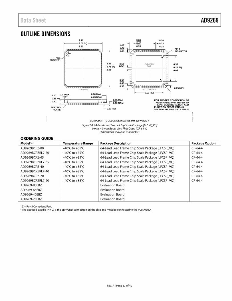
Data Sheet AD9269
Rev. A | Page 37 of 40
OUTLINE DIMENSIONS
COMPLIANT TO JEDEC STANDARDS MO-220-VMMD-4
0.25 MIN
164
1617
4948
3233
0.500.400.30
0.50BSC
0.20 REF
12° MAX 0.80 MAX0.65 NOM
1.000.850.80
7.50 REF
0.05 MAX0.02 NOM
SEATINGPLANE
PIN 1INDICATOR
6.356.20 SQ6.05
PIN 1INDICATOR
0.300.230.18
0.600.420.24
0.600.420.24
FOR PROPER CONNECTION OFTHE EXPOSED PAD, REFER TOTHE PIN CONFIGURATION ANDFUNCTION DESCRIPTIONSSECTION OF THIS DATA SHEET.
TOP VIEW
EXPOSEDPAD
BOTTOM VIEW
9.109.00 SQ8.90
8.858.75 SQ8.65
01-2
2-20
15-D
PKG
-118
4
Figure 60. 64-Lead Lead Frame Chip Scale Package [LFCSP_VQ]
9 mm × 9 mm Body, Very Thin Quad (CP-64-4) Dimensions shown in millimeters
ORDERING GUIDE Model1, 2 Temperature Range Package Description Package Option AD9269BCPZ-80 –40°C to +85°C 64-Lead Lead Frame Chip Scale Package (LFCSP_VQ) CP-64-4 AD9269BCPZRL7-80 –40°C to +85°C 64-Lead Lead Frame Chip Scale Package (LFCSP_VQ) CP-64-4 AD9269BCPZ-65 –40°C to +85°C 64-Lead Lead Frame Chip Scale Package (LFCSP_VQ) CP-64-4 AD9269BCPZRL7-65 –40°C to +85°C 64-Lead Lead Frame Chip Scale Package (LFCSP_VQ) CP-64-4 AD9269BCPZ-40 –40°C to +85°C 64-Lead Lead Frame Chip Scale Package (LFCSP_VQ) CP-64-4 AD9269BCPZRL7-40 –40°C to +85°C 64-Lead Lead Frame Chip Scale Package (LFCSP_VQ) CP-64-4 AD9269BCPZ-20 –40°C to +85°C 64-Lead Lead Frame Chip Scale Package (LFCSP_VQ) CP-64-4 AD9269BCPZRL7-20 –40°C to +85°C 64-Lead Lead Frame Chip Scale Package (LFCSP_VQ) CP-64-4 AD9269-80EBZ Evaluation Board AD9269-65EBZ Evaluation Board AD9269-40EBZ Evaluation Board AD9269-20EBZ Evaluation Board 1 Z = RoHS Compliant Part. 2 The exposed paddle (Pin 0) is the only GND connection on the chip and must be connected to the PCB AGND.

AD9269 Data Sheet
Rev. A | Page 38 of 40
NOTES

Data Sheet AD9269
Rev. A | Page 39 of 40
NOTES

AD9269 Data Sheet
Rev. A | Page 40 of 40
NOTES
©2010–2016 Analog Devices, Inc. All rights reserved. Trademarks and registered trademarks are the property of their respective owners. D08538-0-8/16(A)