Embed Size (px)
Citation preview

General DescriptionThe MAX15035 pulse-width modulation (PWM) control-ler provides high efficiency, excellent transient response, and high DC-output accuracy. Combined with the internal low on-resistance MOSFETs, the MAX15035 provides a highly efficient and compact solution for small form factor applications that need a high-power density.Maxim’s proprietary Quick-PWM™ quick-response, con-stant on-time PWM control scheme handles wide input/output voltage ratios (low-duty-cycle applications) with ease and provides 100ns instant-on response to load transients while maintaining a relatively constant switch-ing frequency. The output voltage can be dynamically controlled using the dynamic REFIN, which supports input voltages between 0V to 2V. The REFIN adjustability combined with a resistive voltage-divider on the feedback input allows the MAX15035 to be configured for any out-put voltage between 0V to 0.9VIN.The controller senses the current across the synchronous rectifier to achieve a low-cost and highly efficient valley current-limit protection. External current-limit control is provided to allow higher current-limit settings for appli-cations with heatsinks and air flow, or for lower current applications that need lower current-limit settings to avoid overdesigning the application circuit. The adjustable cur-rent limit provides a high degree of flexibility, allowing thermally compensated protection or foldback current-limit protection using a voltage-divider partially derived from the output.The MAX15035 includes a voltage-controlled soft-start and soft-shutdown to limit the input surge current, provide a monotonic power-up into a precharged output, and provide a predictable soft-start time. The controller also includes output fault protection—undervoltage and over-voltage protection—as well as thermal-fault protection.The MAX15035 is available in a small 40-pin, 6mm x 6mm, TQFN package.
Features 4.5V to 26V Input Voltage Range Fast Transient Response Monotonic Power-Up with Precharged Output Supports Any Output Capacitor
• No Compensation Required with Polymers/ Tantalum
• Stable with Ceramic Output Capacitors Using External Compensation
Dynamically Adjustable Output Voltage• 0.5% VOUT Accuracy Over Line and Load
Adjustable Valley Current-Limit Protection• Thermal Compensation with NTC• Supports Foldback Current Limit
Programmable Switching Frequency Overvoltage Protection Undervoltage Protection Voltage Soft-Start and Soft-Shutdown Power-Good Window Comparator
Applications Server Computers GPU Core Supplies DDR Memory—VDDQ or VTT Point-of-Load Applications Step-Down Power Supplies Storage Power Supplies
19-4123; Rev 3; 4/18
Quick-PWM is a trademark of Maxim Integrated Products, Inc.
Ordering Information appears at end of data sheet.
MAX15035 15A Step-Down Regulator with Internal Switches
EVALUATION KIT AVAILABLE
Click here for production status of specific part numbers.
IN to PGND ...........................................................-0.3V to +28VTON to GND ..........................................................-0.3V to +28VVDD to GND ............................................................-0.3V to +6VVCC to GND ............................................. -0.3V to (VDD + 0.3V)EN, SKIP, PGOOD to GND.....................................-0.3V to +6VREF, REFIN to GND ................................. -0.3V to (VCC + 0.3V)ILIM, FB to GND ....................................... -0.3V to (VCC + 0.3V)GND to PGND ......................................................-0.3V to +0.3VLX to PGND..............................................................-1V to +28VBST to PGND ............................................ (VDD - 0.3V) to +34VBST to LX ................................................................-0.3V to +6V
BST to VDD ...........................................................-0.3V to +28VREF Short Circuit to GND .........................................ContinuousIN RMS Current Rating (continuous) ....................................15APGND RMS Current Rating (continuous)..............................20AContinuous Power Dissipation (TA = +70°C)
40-Pin, 6mm x 6mm Thin QFN (T4066-MCM) (derate 27mW/°C above +70°C) ...............................2162mW Operating Temperature Range ....................... -40°C to +85°C
Junction Temperature Range ..........................................+150°CStorage Temperature Range ............................ -65°C to +150°CLead Temperature (soldering, 10s) .................................+300°C
(Circuit of Figure 1, VIN = 12V, VDD = VCC = VEN = 5V, REFIN = ILIM = REF, SKIP = GND. TA = 0°C to +85°C, unless otherwise specified. Typical values are at TA = +25°C.) (Note 1)
PARAMETER SYMBOL CONDITIONS MIN TYP MAX UNITSPWM CONTROLLERInput Voltage Range VIN 4.5 26.0 VQuiescent Supply Current (VDD) IDD + ICC FB forced above REFIN 0.7 1.2 mAShutdown Supply Current (VDD) ISHDN EN = GND, TA = +25°C 0.1 2 µA
VCC Undervoltage Lockout Threshold VUVLO(VCC)
Rising edge, PWM disabled below this level; hysteresis = 100mV 3.95 4.2 4.45 V
VDD-to-VCC Resistance RCC 20 Ω
On-Time tON
VIN = 12V,VFB = 1.0V (Note 3)
RTON = 97.5kΩ (600kHz) 123 164 205 nsRTON = 200kΩ (300kHz) 275 303 331RTON = 302.5kΩ (200kHz) 379 442 505
Minimum Off-Time tOFF(MIN) (Note 3) 225 350 ns
TON Shutdown Supply Current EN = GND, VTON = 26V,VCC = 0V or 5V, TA = +25°C 0.01 1 µA
REFIN Voltage Range VREFIN (Note 2) 0 VREF V
PACKAGE TYPE: 40-PIN TQFNPackage Code T4066M+1Outline Number 21-0177Land Pattern Number 90-0085
MAX15035 15A Step-Down Regulator with Internal Switches
www.maximintegrated.com Maxim Integrated 2
Absolute Maximum Ratings
Stresses beyond those listed under “Absolute Maximum Ratings” may cause permanent damage to the device. These are stress ratings only, and functional operation of the device at these or any other conditions beyond those indicated in the operational sections of the specifications is not implied. Exposure to absolute maximum rating conditions for extended periods may affect device reliability.
Electrical Characteristics 1
For the latest package outline information and land patterns (footprints), go to www.maximintegrated.com/packages. Note that a “+”, “#”, or “-” in the package code indicates RoHS status only. Package drawings may show a different suffix character, but the drawing pertains to the package regardless of RoHS status.
Package Information

(Circuit of Figure 1, VIN = 12V, VDD = VCC = VEN = 5V, REFIN = ILIM = REF, SKIP = GND. TA = 0°C to +85°C, unless otherwise specified. Typical values are at TA = +25°C.) (Note 1)
PARAMETER SYMBOL CONDITIONS MIN TYP MAX UNITSREFIN Input Current IREFIN TA = +25°C, REFIN = 0.5V to 2V -50 +50 nAFB Voltage Range VFB (Note 2) 0 VREF V
FB Voltage Accuracy VFB
VREFIN = 0.5V, measured at FB,VIN = 4.5V to 26V, SKIP = VDD
TA = +25°C 0.495 0.5 0.505
VTA = 0°C to +85°C 0.493 0.507
VREFIN = 1.0VTA = +25°C 0.995 1.0 1.005TA = 0°C to +85°C 0.993 1.007
VREFIN = 2.0V TA = 0°C to +85°C 1.990 2.0 2.010FB Input Bias Current IFB VFB = 0.5V to 2.0V, TA = +25°C -0.1 +0.1 µAFB Output Low Voltage ISINK = 3mA 0.4 VLoad-Regulation Error SKIP = VDD 0.1 %Line-Regulation Error VCC = 4.5V to 5.5V, VIN = 4.5V to 26V 0.2 %Soft-Start/Soft-Stop Slew Rate SSSR Rising/falling edge on EN 0.4 1.2 2.2 mV/µsDynamic REFIN Slew Rate DYNSR Rising edge on REFIN 3 9.45 18 mV/µsREFERENCE
Reference Voltage VREFVCC = 4.5Vto 5.5V
No load 1.990 2.00 2.010V
IREF = -10µA to +50µA 1.98 2.02FAULT DETECTION
Output Overvoltage-Protection Trip Threshold OVP
With respect to the internal target voltage (error comparator threshold); rising edge; hysteresis = 50mV
250 300 350 mV
Dynamic transition VREF + 0.30 V
Minimum OVP threshold 0.7Output OvervoltageFault-Propagation Delay tOVP FB forced 25mV above trip threshold 5 µs
Output Undervoltage-Protection Trip Threshold UVP
With respect to the internal target voltage (error comparator threshold) falling edge; hysteresis = 50mV
-240 -200 -160 mV
Output UndervoltageFault-Propagation Delay tUVP FB forced 25mV below trip threshold 100 200 350 µs
PGOOD Propagation Delay tPGOOD
UVP falling edge, 25mV overdrive 5µsOVP rising edge, 25mV overdrive 5
Startup delay 100 200 350PGOOD Output-Low Voltage ISINK = 3mA 0.4 V
PGOOD Leakage Current IPGOODFB = REFIN (PGOOD high impedance), PGOOD forced to 5V, TA = +25°C 1 µA
MAX15035 15A Step-Down Regulator with Internal Switches
www.maximintegrated.com Maxim Integrated 3
Electrical Characteristics 1 (continued)

(Circuit of Figure 1, VIN = 12V, VDD = VCC = VEN = 5V, REFIN = ILIM = REF, SKIP = GND. TA = 0°C to +85°C, unless otherwise specified. Typical values are at TA = +25°C.) (Note 1)
(Circuit of Figure 1, VIN = 12V, VDD = VCC = VEN = 5V, REFIN = ILIM = REF, SKIP = GND. TA = -40°C to +85°C, unless otherwise specified.) (Note 1)
PARAMETER SYMBOL CONDITIONS MIN MAX UNITSPWM CONTROLLERInput Voltage Range VIN 4.5 26 VQuiescent Supply Current (VDD) IDD + ICC FB forced above REFIN 1.2 mA
On-Time tON
VIN = 12V,VFB = 1.0V (Note 3)
RTON = 97.5kΩ (600kHz) 115 213nsRTON = 200kΩ (300kHz) 270 336
RTON = 302.5kΩ (200kHz) 368 516Minimum Off-Time tOFF(MIN) (Note 3) 400 nsREFIN Voltage Range VREFIN (Note 2) 0 VREF V
PARAMETER SYMBOL CONDITIONS MIN TYP MAX UNITS
Dynamic REFIN Transition Fault Blanking Threshold
Fault blanking initiated; REFIN deviation from the internal target voltage (error comparator threshold); hysteresis = 10mV
±50 mV
Thermal-Shutdown Threshold TSHDN Temperature rising, hysteresis = 15°C 160 °CCURRENT LIMITILIM Input Range 0.4 VREF VILIM Input Bias Current TA = +25°C, ILIM = 0.4V to 2V -0.1 +0.1 µA
Current-Limit Threshold VILIMITVILIM = 0.4V, VGND - VLX 18 20 22
mVILIM = REF (2.0V), VGND - VLX 92 100 108
Current-Limit Threshold(Negative) VINEG VILIM = 0.4V, VGND - VLX -24 mV
Current-Limit Threshold(Zero Crossing) VZX
VILIM = 0.4V,VGND - VLX, SKIP = GND or open 1 mV
Ultrasonic Frequency SKIP = open (3.3V); VFB = VREFIN + 50mV 18 30 kHzUltrasonic Current-LimitThreshold
SKIP = open (3.3V); VFB = VREFIN + 50mV,VGND - VLX
-35 mV
Internal BST SwitchOn-Resistance RBST IBST = 10mA, VDD = 5V 4 7 Ω
INPUTS AND OUTPUTSEN Logic-Input Threshold VEN EN rising edge, hysteresis = 450mV (typ) 1.20 1.7 2.20 VEN Logic-Input Current IEN EN forced to GND or VDD, TA = +25°C -0.5 +0.5 µA
SKIP Quad-Level Input Logic Levels VSKIP
High (5V VDD) VCC - 0.4
VOpen (3.3V) 3.0 3.6Ref (2.0V) 1.7 2.3Low (GND) 0.4
SKIP Logic-Input Current ISKIP SKIP forced to GND or VDD, TA = +25°C -2 +2 µA
MAX15035 15A Step-Down Regulator with Internal Switches
www.maximintegrated.com Maxim Integrated 4
Electrical Characteristics 1 (continued)
Electrical Characteristics 2
(Circuit of Figure 1, VIN = 12V, VDD = VCC = VEN = 5V, REFIN = ILIM = REF, SKIP = GND. TA = -40°C to +85°C, unless otherwise specified.) (Note 1)
Note 1: Limits are 100% production tested at TA = +25°C. Maximum and minimum limits over temperature are guaranteed by design and characterization.
Note 2: The 0 to 0.5V range is guaranteed by design, not production tested.Note 3: On-time and off-time specifications are measured from 50% point to 50% point at the unloaded LX node. The typical 25ns
dead time that occurs between the high-side driver falling edge (high-side MOSFET turn-off) and the low-side MOSFET turnon) is included in the on-time measurement. Similarly, the typical 25ns dead time that occurs between the low-side driver falling edge (low-side MOSFET turn-off) and the high-side driver rising edge (high-side MOSFET turn-on) is included in the off-time measurement.
FB Voltage Range VFB (Note 2) 0 VREF V
FB Voltage Accuracy VFB
Measured at FB,VIN = 4.5V to 26V, SKIP = VDD
VREFIN = 0.5V 0.49 0.51VVREFIN = 1.0V 0.99 1.01
VREFIN = 2.0V 1.985 2.015PARAMETER SYMBOL CONDITIONS MIN MAX UNITS
REFERENCEReference Voltage VREF VDD = 4.5V to 5.5V 1.985 2.015 VFAULT DETECTION
Output Overvoltage-Protection Trip Threshold OVP
With respect to the internal target voltage (error comparator threshold) rising edge; hysteresis = 50mV
250 350 mV
Output Undervoltage-Protection Trip Threshold UVP
With respect to the internal target voltage (error comparator threshold);falling edge; hysteresis = 50mV
-240 -160 mV
Output UndervoltageFault-Propagation Delay tUVP FB forced 25mV below trip threshold 80 400 µs
PGOOD Output-Low Voltage ISINK = 3mA 0.4 VVCC Undervoltage Lockout Threshold VUVLO(VCC)
Rising edge, PWM disabled below this level,hysteresis = 100mV 3.95 4.45 V
CURRENT LIMITILIM Input Range 0.4 VREF V
Current-Limit Threshold VILIMITVILIM = 0.4V, VGND = VLX 17 23
mVILIM = REF (2.0V), VGND - VLX 90 110
Ultrasonic Frequency SKIP = open (3.3V), VFB = VREFIN + 50mV 17 kHzINPUTS AND OUTPUTSEN Logic-Input Threshold VEN EN rising edge hysteresis = 450mV (typ) 1.20 2.20 V
SKIP Quad-Level InputLogic Levels V SKIP
High (5V VDD) VCC - 0.4
VMid (3.3V) 3.0 3.6Ref (2.0V) 1.7 2.3Low (GND) 0.4
MAX15035 15A Step-Down Regulator with Internal Switches
www.maximintegrated.com Maxim Integrated 5
Electrical Characteristics 2 (continued)

(MAX15035 Circuit of Figure 1, VIN = 12V, VDD = 5V, SKIP = GND, RTON = 200kΩ, TA = +25°C, unless otherwise noted.)
1.5V OUTPUT EFFICIENCYvs. LOAD CURRENT
MAX
1503
5 to
c02
LOAD CURRENT (A)
EFFI
CIEN
CY (%
)
1010.1
30
40
50
60
70
80
90
100
200.01 100
SKIP MODE
PWM MODE
ULTRASONIC MODE
1.5V OUTPUT VOLTAGEvs. LOAD CURRENT
MAX
1503
5 to
c03
LOAD CURRENT (A)
OUTP
UT V
OLTA
GE (V
)
1413121110987654321
1.495
1.505
1.515
1.4850 15
SKIP MODEPWM MODE
ULTRASONIC MODE
1.05V OUTPUT EFFICIENCYvs. LOAD CURRENT
MAX
1503
5 to
c04
LOAD CURRENT (A)
EFFI
CIEN
CY (%
)
1010.1
30
40
50
60
70
80
90
100
200.01 100
SKIP MODEPWM MODE
7V
20V20V
12V
12V
1.05V OUTPUT EFFICIENCYvs. LOAD CURRENT
MAX
1503
5 to
c05
LOAD CURRENT (A)
EFFI
CIEN
CY (%
)
1010.1
30
40
50
60
70
80
90
100
200.01 100
SKIP MODE
PWM MODE
ULTRASONIC MODE
1.05V OUTPUT VOLTAGEvs. LOAD CURRENT
MAX
1503
5 to
c06
LOAD CURRENT (A)
OUTP
UT V
OLTA
GE (V
)
1413121110987654321
1.05
1.06
1.040 15
ULTRASONIC MODE
SKIP MODE
PWM MODE
3.3V OUTPUT EFFICIENCYvs. LOAD CURRENT
MAX
1503
5 to
c07
LOAD CURRENT (A)
EFFI
CIEN
CY (%
)
1010.1
30
40
50
60
70
80
90
100
200.01 100
20V
12V
7V
SKIP MODEPWM MODE
1.5V OUTPUT EFFICIENCYvs. LOAD CURRENT
MAX
1503
5 to
c01
LOAD CURRENT (A)
EFFI
CIEN
CY (%
)
1010.1
30
40
50
60
70
80
90
100
200.01 100
SKIP MODEPWM MODE
7V20V
12V
3.3V OUTPUT EFFICIENCYvs. LOAD CURRENT
MAX
1503
5 to
c08
LOAD CURRENT (A)
EFFI
CIEN
CY (%
)
1010.1
30
40
50
60
70
80
90
100
200.01 100
SKIP MODE
PWM MODE
ULTRASONIC MODE
3.3V OUTPUT VOLTAGEvs. LOAD CURRENT
MAX
1503
5 to
c09
LOAD CURRENT (A)
OUTP
UT V
OLTA
GE (V
)
1413121110987654321
3.380
3.3653.350
3.3203.305
3.2903.2753.2603.245
3.335
3.2300 15
ULTRASONIC MODE
PWM MODESKIP MODE
MAX15035 15A Step-Down Regulator with Internal Switches
Maxim Integrated 6www.maximintegrated.com
Typical Operating Characteristics
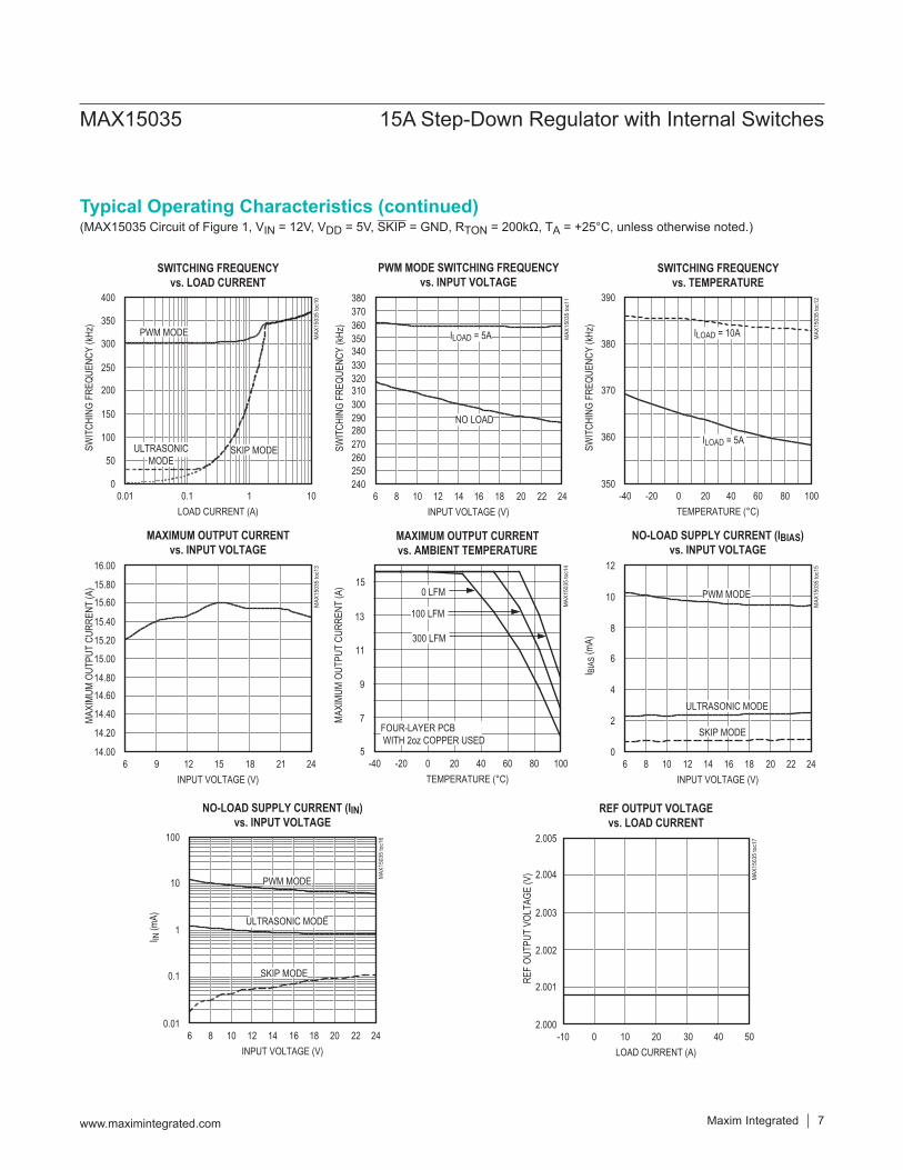
(MAX15035 Circuit of Figure 1, VIN = 12V, VDD = 5V, SKIP = GND, RTON = 200kΩ, TA = +25°C, unless otherwise noted.)
SWITCHING FREQUENCYvs. LOAD CURRENT
MAX
1503
5 to
c10
LOAD CURRENT (A)
SWIT
CHIN
G FR
EQUE
NCY
(kHz)
10.1
50
100
150
200
250
300
350
400
00.01 10
SKIP MODEULTRASONICMODE
PWM MODE
PWM MODE SWITCHING FREQUENCYvs. INPUT VOLTAGE
MAX
1503
5 to
c11
INPUT VOLTAGE (V)
SWIT
CHIN
G FR
EQUE
NCY
(kHz)
14 1810
350360370
320330340
290300310
260250
270280
380
2406 22 2412 168 20
ILOAD = 5A
NO LOAD
SWITCHING FREQUENCYvs. TEMPERATURE
MAX
1503
5 to
c12
TEMPERATURE (°C)
SWIT
CHIN
G FR
EQUE
NCY
(kHz)
20 40 60 80-20 0
360
380
370
390
350-40 100
ILOAD = 10A
ILOAD = 5A
MAXIMUM OUTPUT CURRENTvs. INPUT VOLTAGE
MAX
1503
5 to
c13
INPUT VOLTAGE (V)
MAXI
MUM
OUTP
UT C
URRE
NT (A
)
15 18 219 12
15.00
14.80
15.60
15.40
15.20
14.40
14.20
14.60
16.00
15.80
14.006 24
MAXIMUM OUTPUT CURRENTvs. AMBIENT TEMPERATURE
MAX
1503
5 to
c14
TEMPERATURE (°C)
MAXI
MUM
OUTP
UT C
URRE
NT (A
)
806040200-20
7
9
11
13
15
5-40 100
0 LFM
100 LFM
300 LFM
FOUR-LAYER PCB WITH 2oz COPPER USED
NO-LOAD SUPPLY CURRENT (IBIAS)vs. INPUT VOLTAGE
MAX
1503
5 to
c15
INPUT VOLTAGE (V)
I BIAS
(mA)
10 12 14 16 18 20 228
4
2
8
6
10
12
06 24
SKIP MODE
PWM MODE
ULTRASONIC MODE
NO-LOAD SUPPLY CURRENT (IIN)vs. INPUT VOLTAGE
MAX
1503
5 to
c16
INPUT VOLTAGE (V)
I IN (m
A)
10 12 14 16 18 20 228
0.1
1
10
100
0.016 24
SKIP MODE
PWM MODE
ULTRASONIC MODE
REF OUTPUT VOLTAGEvs. LOAD CURRENT
MAX
1503
5 to
c17
LOAD CURRENT (A)
REF
OUTP
UT V
OLTA
GE (V
)
10 20 30 400
2.001
2.002
2.003
2.005
2.004
2.000-10 50
MAX15035 15A Step-Down Regulator with Internal Switches
Maxim Integrated 7www.maximintegrated.com
Typical Operating Characteristics (continued)

(MAX15035 Circuit of Figure 1, VIN = 12V, VDD = 5V, SKIP = GND, RTON = 200kΩ, TA = +25°C, unless otherwise noted.)
SOFT-START WAVEFORM(HEAVY LOAD)
MAX15035 toc18
200µs/divC. VOUT, 1V/divB. INDUCTOR CURRENT, 10A/div
1.5V
8A
05V
0
0
0
5V A
B
C
D
A. EN, 5V/divB. PGOOD, 5V/div
IOUT = 8A
SOFT-START WAVEFORM(LIGHT LOAD)
MAX15035 toc19
200µs/divC. VOUT, 1V/divB. INDUCTOR CURRENT, 10A/div
1.5V
05V
0
0
01A
5V A
B
C
D
A. EN, 5V/divB. PGOOD, 5V/divIOUT = 1A
SHUTDOWN WAVEFORMMAX15035 toc20
200µs/divC. VOUT, 1V/divB. INDUCTOR CURRENT, 5A/div
A
B
C
D
A. EN, 5V/divB. PGOOD, 5V/divIOUT = 6A
1.5V
0
5V
0
0
0
8A
5V
LOAD-TRANSIENT RESPONSE(PWM MODE)
MAX15035 toc21
20µs/divB. VOUT, 20mV/divC. INDUCTOR CURRENT, 5A/div
8A
1A
1.5V
8A
0A
A
B
C
A. IOUT, 10A/div
IOUT = 1A TO 8A TO 1A
MAX15035 15A Step-Down Regulator with Internal Switches
Maxim Integrated 8www.maximintegrated.com
Typical Operating Characteristics (continued)

(MAX15035 Circuit of Figure 1, VIN = 12V, VDD = 5V, SKIP = GND, RTON = 200kΩ, TA = +25°C, unless otherwise noted.)
LOAD-TRANSIENT RESPONSE(SKIP MODE)
MAX15035 toc22
20µs/divB. VOUT, 20mV/divC. INDUCTOR CURRENT, 5A/div
8A1A
1.5V
8A0A
A
B
C
A. IOUT, 10A/div
IOUT = 1A TO 8A TO 1A
OUTPUT OVERCURRENT WAVEFORMMAX15035 toc23
200µs/divB. VOUT, 1V/divC. PGOOD, 5V/div
5V
20A
0
1.5V
0
0
A
B
C
A. INDUCTOR CURRENT, 10A/divIOUT = 2A TO 20A
OUTPUT OVERVOLTAGE WAVEFORMMAX15035 toc24
200µs/divB. PGOOD, 5V/div
0
1.5V
5V
0
A
B
A. VOUT, 1V/div
IOUT = 2A TO 20A
NO-LOAD BIAS CURRENTvs. FREQUENCY
MAX
1503
5 to
c25
FREQUENCY (kHz)
I BIAS
(mA)
550500400 450300 350250
1012141618202224262830
8200 600
PWM MODE
OUTPUT CURRENT LIMITvs. ILIMIT VOLTAGE
MAX
1503
5 to
c26
ILIMIT VOLTAGE (mV)
CURR
ENT
LIMIT
(A)
900800700600
10
12
14
16
18
20
8500 1000
PREBIAS STARTUP-OUTPUT VOLTAGEMAX15035 toc27
200µs/div
500mV/div
1.5V
1.2V
MAX15035 15A Step-Down Regulator with Internal Switches
Maxim Integrated 9www.maximintegrated.com
Typical Operating Characteristics (continued)

(MAX15035 Circuit of Figure 1, VIN = 12V, VDD = 5V, SKIP = GND, RTON = 200kΩ, TA = +25°C, unless otherwise noted.)
DYNAMIC OUTPUT-VOLTAGE TRANSITION(PWM MODE)
MAX15035 toc28
40µs/divC. INDUCTOR CURRENT, 10A/divD. LX, 10V/div
-6A0
1.5V
1.5V1.05V
1.05V
12V
0
A
B
C
D
A. REFIN, 500mV/divB. VOUT, 200mV/divIOUT = 2A
DYNAMIC OUTPUT-VOLTAGE TRANSITION(SKIP MODE)
MAX15035 toc29
40µs/divC. INDUCTOR CURRENT, 10A/divD. LX, 10V/div
10A
0
1.5V
1.5V1.05V
1.05V
12V
0
A
B
C
D
A. REFIN, 500mV/divB. VOUT, 200mV/divIOUT = 2A
MAX15035 15A Step-Down Regulator with Internal Switches
www.maximintegrated.com Maxim Integrated 10
Typical Operating Characteristics (continued)

PIN NAME FUNCTION1, 17, 27, 31,
39, 40 N.C. No Connection. Not internally connected.
2 EN
Shutdown Control Input. Connect to VDD for normal operation. Pull EN low to put the controller into its 2µA (max) shutdown state. The MAX15035 slowly ramps down the target/output voltage to ground and after the target voltage reaches 0.1V, the controller forces LX into a high-impedance state and enters the low-power shutdown state. Toggle EN to clear the fault-protection latch.
3, 28 AGND Analog Ground. Internally connected to EP1.
4 VDDSupply Voltage Input for the DL Gate Driver. Connect to the system supply voltage (+4.5V to +5.5V). Bypass VDD to power ground with a 1µF or greater ceramic capacitor.
5, 16 LX Inductor Connection. Internally connected to EP2. Connect LX to the switched side of the inductor as shown in Figure 1.
6–15 PGND Power Ground18–26 IN Power MOSFET Input Power Source. Internally connected to EP3.
29 TON
Switching Frequency-Setting Input. An external resistor between the input power source and TON sets the switching period (tSW = 1/fSW) according to the following equation: FB
SW TON TONOUT
Vt C (R 6.5k )V
= + Ω
where CTON = 16.26pF and VFB = VREFIN under normal operating conditions. If the TON current drops below 10µA, the MAX15035 shuts down and enters a high-impedance state. TON is high impedance in shutdown.
30 BST Boost Flying Capacitor Connection. Connect to an external 0.1µF capacitor as shown in Figure 1. The MAX15035 contains an internal boost switch/diode (Figure 2).
MAX15035
THIN QFN(6mm x 6mm)
TOP VIEW
35
36
34
33
12
11
13
EN V DD LX
PGND
PGND
14
N.C.
N.C.
IN INAGND
TON
BST
IN IN
1 2
REFIN
4 5 6 7
27282930 26 24 23 22
REF
SKIP
IN
N.C.
LX
PGNDAG
ND
IN
3
25
37VCC PGND
38
39
40
PGOOD
N.C.
N.C.
PGND
PGND
PGND
ILIM
32
15
INFB
31
16
17
18
19
20 IN
PGND
PGND
PGND
IN
8 9 10
21
N.C.
+
EP1 EP3
AGND
IN
LX
EP2
MAX15035 15A Step-Down Regulator with Internal Switches
www.maximintegrated.com Maxim Integrated 11
Pin Description
Pin Configuration

PIN NAME FUNCTION
32 FB
Feedback Voltage Sense Connection. Connect directly to the positive terminal of the output capacitors for output voltages less than 2V as shown in Figure 1. For fixed-output voltages greater than 2V, connect REFIN to REF and use a resistive divider to set the output voltage (Figure 6). FB senses the output voltage to determine the on-time for the high-side switching MOSFET.
33 ILIMCurrent-Limit Threshold Adjustment. The current-limit threshold is 0.05 times (1/20) the voltage at ILIM. Connect ILIM to a resistive divider (from REF) to set the current-limit threshold between 20mV and 100mV (with 0.4V to 2V at ILIM).
34 REFIN
External Reference Input. REFIN sets the feedback regulation voltage (VFB = VREFIN) of the MAX15035 using a resistor-divider connected between REF and AGND. The MAX15035 includes an internal window comparator to detect REFIN voltage transitions, allowing the controller to blank PGOOD and the fault protection.
35 REF 2V Reference Voltage. Bypass to analog ground using a 1nF ceramic capacitor. The reference can source up to 50µA for external loads.
36 SKIP
Pulse-Skipping Control Input. This four-level input determines the mode of operation under normal steady-state conditions and dynamic output-voltage transitions:VDD (5V) = Forced-PWM operationREF (2V) = Pulse-skipping mode (with forced-PWM during transitions)Open (3.3V) = Ultrasonic mode (without forced-PWM during transitions)GND = Pulse-skipping mode (without forced-PWM during transitions)
37 VCC5V Analog Supply Voltage. Internally connected to VDD through an internal 20Ω resistor. Bypass VCC to analog ground using a 1µF ceramic capacitor.
38 PGOOD
Open-Drain Power-Good Output. PGOOD is low when the output voltage is more than 200mV (typ) below or 300mV (typ) above the target voltage (VREFIN), during soft-start, and soft-shutdown. After the soft-start circuit has terminated, PGOOD becomes high impedance if the output is in regulation. PGOOD is blanked—forced high-impedance state—when a dynamic REFIN transition is detected.
EP1(41) AGND Exposed Pad 1/Analog Ground. Internally connected to the controller’s ground plane and substrate.
Connect directly to ground.
EP2(42) LX
Exposed Pad 2/Inductor Connection. Internally connected to drain of the low-side MOSFET and source of the high-side MOSFET (Figure 2). Connect LX to the switched side of the inductor as shown in Figure 1.
EP3(43) IN Exposed Pad 3/Power MOSFET Input Power Source. Internally connected to drain of the high-side
MOSFET (Figure 2).
MAX15035 15A Step-Down Regulator with Internal Switches
www.maximintegrated.com Maxim Integrated 12
Pin Description (continued)

Figure 1. MAX15035 Standard Application Circuit
Table 1. Component Selection for Standard Applications
Table 2. Component Suppliers
COMPONENT
VOUT = 1.5V/1.05V AT 15A(Figure 1)
VOUT = 3.3V AT 6A(Figure 6)
VOUT = 1.5V/1.05V AT 10A(Figure 1)
VIN = 7V to 20VTON = 200kΩ (300kHz)
VIN = 7V to 20VTON = 332kΩ (300kHz)
VIN = 5V to 12VTON = 100kΩ (600kHz)
Input Capacitor (3x) 10µF, 25VTaiyo Yuden TMK432BJ106KM
(2x) 10µF, 25VTaiyo Yuden TMK432BJ106KM
(3x) 10µF, 25VTaiyo Yuden TMK432BJ106KM
Output Capacitor (2x) 330µF, 6mΩ, 2VPanasonic EEFSX0D331XR
(1x) 330µF, 18mΩ, 4VSANYO 4TPE330MI
(1x) 470µF, 7mΩ, 2.5VSANYO 2R5TPLF470M7
Inductor 1.0µH, 5.3mΩ, 27.5AVishay IHLP4040DZER1R0
1.5µH, 14mΩ, 9ANEC TOKIN MPLC1040L3R3
0.47µH, 3.7mΩ, 15ACooper FP3-R47-R
SUPPLIER WEBSITEAVX Corp. www.avxcorp.comBI Technologies www.bitechnologies.comCooper Bussmann www.cooperet.comKEMET Corp. www.kemet.comMurata Mfg. Co., Ltd. www.murata.comNEC TOKIN Corp. www.nec-tokin.com Panasonic Corp. www.panasonic.com
SUPPLIER WEBSITEPulse Engineering www.pulseeng.comSANYO NA Corp. www.sanyo.com Sumida Corp. www.sumida.comTaiyo Yuden www.t-yuden.comTDK Corp. www.component.tdk.com TOKO America, Inc. www.tokoam.com Vishay www.vishay.comWürth Electronik GmbH & Co. KG www.we-online.com
C11µF
ENOFFON
VDD
VCC
C21µF
PGOOD
R10100kΩ
REFINR2
54.9kΩ
R440.2kΩ
RT60.4kΩ
NTC10kΩ
B = 3435R549.4kΩ
BST
LX
CBST0.1µF L1
COUT
TON
R397.6kΩ
GND/OPEN/REF/VDD
PGND
FB
ILIM
HILO
REF
RTON200kΩ
AGND
AGND
PWR
PWRPWR
AGND
AGND
AGND
2
34
36
4
37
18–26, EP330
6–15
AGND
38
SKIP
35
32
33
OUTPUT1.05V/1.50V15A (MAX)
INPUT7V TO 24V
5V BIASSUPPLY
MAX15035
CIN
PWR
C31000pF
R149.9kΩ
5, 16, EP2
29
IN
3, 28, EP1
PWRSEE TABLE 1 FOR COMPONENT SELECTION.
MAX15035 15A Step-Down Regulator with Internal Switches
www.maximintegrated.com Maxim Integrated 13
Standard Application CircuitThe MAX15035 standard application circuit (Figure 1) generates a 1.5V or 1.05V output rail for general-purpose use. See Table 1 for component selections. Table 2 lists the component suppliers.
Detailed DescriptionThe MAX15035 step-down controller is ideal for low-duty-cycle (high-input voltage to low-output voltage) applications. Maxim’s proprietary Quick-PWM pulse-width modulator in the MAX15035 is specifically designed for handling fast-load steps while maintaining a relatively constant operating frequency and inductor operating point over a wide range of input voltages. The Quick-PWM architecture circumvents the poor load-transient timing problems of fixed-frequency, current-mode PWMs while also avoiding the problems caused by widely varying switching frequencies in conventional constant-on-time (regardless of input voltage) pulse-frequency modulation (PFM) control schemes.
+5V Bias Supply (VCC/VDD)The MAX15035 requires an external 5V bias supply in addition to the input. See Figure 6 for an optional 5V bias generation circuit.The 5V bias supply powers both the PWM controller and internal gate-drive power, so the maximum current drawn is determined by:
IBIAS = IQ + fSWQG = 2mA to 20mA (typ)The MAX15035 includes a 20Ω resistor between VDD and VCC, simplifying the PCB layout requirement.
Free-Running Constant-On-Time PWM Controller with Input Feed-ForwardThe Quick-PWM control architecture is a pseudo-fixed-frequency, constant on-time, current-mode regulator with voltage feed-forward (Figure 2). This architecture relies on the output filter capacitor’s ESR to act as a current-sense resistor, so the output ripple voltage provides the PWM ramp signal. The control algorithm is simple: the high-side switch on-time is determined solely by a one-shot whose pulse width is inversely proportional to input voltage and directly proportional to output voltage. Another one-shot sets a minimum offtime (200ns typ). The on-time one-shot is triggered if the error comparator is low, the low-side switch current is below the valley current-limit threshold, and the minimum off-time one-shot has timed out.
On-Time One-ShotThe heart of the PWM core is the one-shot that sets the high-side switch on-time. This fast, low-jitter, adjust-able one-shot includes circuitry that varies the on-time in response to input and output voltage. The high-side switch on-time is inversely proportional to the input volt-age as sensed by the TON input, and proportional to the feedback voltage as sensed by the FB input:
On-Time (tON) = tSW (VFB/VIN)where tSW (switching period) is set by the resistance (RTON) between TON and IN. This algorithm results in a nearly constant switching frequency despite the lack of a fixed-frequency clock generator. Connect a resistor (RTON) between TON and IN to set the switching period tSW = 1/fSW:
( ) FBSW TON TON
OUT
Vt C R 6.5kV
= + Ω
where CTON = 16.26pF. When used with unity-gain feedback (VOUT = VFB), a 96.75kΩ to 303.25kΩ corresponds to switching periods of 167ns (600kHz) to 500ns (200kHz), respectively. High-frequency (600kHz) operation optimizes the application for the smallest component size, trading off efficiency due to higher switching losses. This may be acceptable in ultra-portable devices where the load currents are lower and the controller is powered from a lower voltage supply. Low-frequency (200kHz) operation offers the best overall efficiency at the expense of component size and board space.For continuous conduction operation, the actual switching frequency can be estimated by:
FB DISSW
ON IN CHG
V Vft (V V )
+=
−
where VDIS is the sum of the parasitic voltage drops in the inductor discharge path, including synchronous rectifier, inductor, and PCB resistances; VCHG is the sum of the resistances in the charging path, including the highside switch, inductor, and PCB resistances; and tON is the on-time calculated by the MAX15035.
Power-Up Sequence (POR, UVLO)The MAX15035 is enabled when EN is driven high and the 5V bias supply (VDD) is present. The reference powers up first. Once the reference exceeds its UVLO threshold, the internal analog blocks are turned on and masked by a 50μs one-shot delay in order to allow the bias circuitry and analog blocks enough time to settle to their proper
MAX15035 15A Step-Down Regulator with Internal Switches
www.maximintegrated.com Maxim Integrated 14

Figure 2. MAX15035 Block Diagram
DYNAMIC OUTPUTTRANSITION DETECTION
BST
LX
ONE-SHOTTRIGQ
tOFF(MIN)ON-TIME
COMPUTEFB
TON
ERRORAMPLIFIER
EA + 0.3V
ONE-SHOT
TRIG QtON
ZERO CROSSING
FB
EAPGOOD
EN
PGOODAND FAULT
PROTECTION
SKIP
EA - 0.2V
BLANK
REFIN
VALLEY CURRENT LIMIT
PGND
S
RQ
S
R
Q
IN
SOFT-START/SOFT-STOP
QUAD-LEVEL
DECODEBLANK
VCC
VDD
2VREF
FAUL
T
INTEGRATOR(CCV)
REF
ILIM
MAX15035
IN
MAX15035 15A Step-Down Regulator with Internal Switches
www.maximintegrated.com Maxim Integrated 15

states. With the control circuitry reliably powered up, the PWM controller may begin switching.Power-on reset (POR) occurs when VCC rises above approximately 3V, resetting the fault latch and preparing the controller for operation. The VCC UVLO circuitry inhib-its switching until VCC rises above 4.25V. The controller powers up the reference once the system enables the controller, VCC exceeds 4.25V, and EN is driven high. With the reference in regulation, the controller ramps the output voltage to the target REFIN voltage with a 1.2mV/μs slew rate:
FB FBSTART
V Vt1.2mV µs 1.2V ms
= =
The soft-start circuitry does not use a variable current limit, so full output current is available immediately. PGOOD becomes high impedance approximately 200μs after the target REFIN voltage has been reached. The MAX15035 automatically uses pulse-skipping mode during soft-start and uses forced-PWM mode during soft-shutdown, regardless of the SKIP configuration.For automatic startup, the input voltage should be present before VCC. If the controller attempts to bring the output into regulation without the input voltage present, the fault latch trips. The controller remains shut down until the fault latch is cleared by toggling EN or cycling the VCC power supply below 0.5V.If the VCC voltage drops below 4.25V, the controller assumes that there is not enough supply voltage to make valid decisions. To protect the output from overvoltage faults, the controller shuts down immediately and forces a high impedance on LX.
ShutdownWhen the system pulls EN low, the MAX15035 enters low-power shutdown mode. PGOOD is pulled low immediately, and the output voltage ramps down with a 1.2mV/μs slew rate:
FB FBSHDN
V Vt1.2mV µs 1.2V ms
= =
Slowly discharging the output capacitors by slewing the output over a long period of time (typically 0.5ms to 2ms) keeps the average negative inductor current low (damped response), thereby preventing the negative output-voltage excursion that occurs when the controller discharges the output quickly by permanently turning on the low-side MOSFET (underdamped response). This eliminates the need for the Schottky diode normally connected between the output and ground to clamp the negative output-voltage
excursion. After the controller reaches the zero target, the MAX15035 shuts down completely—the drivers are disabled (high impedance on LX)—the reference turns off, and the supply currents drop to about 0.1μA (typ).When a fault condition—output UVP or thermal shut-down—activates the shutdown sequence, the protection circuitry sets the fault latch to prevent the controller from restarting. To clear the fault latch and reactivate the con-troller, toggle EN or cycle VCC power below 0.5V.The MAX15035 automatically uses pulse-skipping mode during soft-start and uses forced-PWM mode during soft-shutdown, regardless of the SKIP configuration.
Modes of OperationUltrasonic Mode (SKIP = Open = 3.3V)Leaving SKIP unconnected activates a unique pulseskip-ping mode with a minimum switching frequency of 18kHz. This ultrasonic pulse-skipping mode eliminates audio-fre-quency modulation that would otherwise be present when a lightly loaded controller automatically skips pulses. In ultrasonic mode, the controller automatically transitions to fixed-frequency PWM operation when the load reaches the same critical conduction point (ILOAD(SKIP)) that occurs when normally pulse skipping.An ultrasonic pulse occurs when the controller detects that no switching has occurred within the last 33μs. Once triggered, the ultrasonic controller turns on the low-side MOSFET to induce a negative inductor current (Figure 3). After the inductor current reaches the negative ultrasonic current threshold, the controller turns off the low-side MOSFET and triggers a constant on-time.
Figure 3. Ultrasonic Waveform
ON-TIME (tON)ISONIC
ZERO-CROSSINGDETECTION
0
33µs (typ)
INDUCTORCURRENT
MAX15035 15A Step-Down Regulator with Internal Switches
www.maximintegrated.com Maxim Integrated 16

When the on-time expires, the controller re-enables the low-side MOSFET until the controller detects that the inductor current drops below the zero-crossing threshold. Starting with a negative inductor current pulse greatly reduces the peak output voltage when compared to start-ing with a positive inductor current pulse.The output voltage at the beginning of the ultrasonic pulse determines the negative ultrasonic current threshold, resulting in the following equation:
( )ISONIC L REFIN FBV I 0.006 V V 0.7= × = − ×
where VFB > VREFIN.
Forced-PWM Mode (SKIP = VDD)The low-noise, forced-PWM mode (SKIP = VDD) disables the zero-crossing comparator, which controls the low-side switch on-time. This forces the low-side gate-drive waveform to constantly be the complement of the high-side gate-drive waveform, so the inductor current reverses at light loads while LX maintains a duty factor of VOUT/VIN. The benefit of forced-PWM mode is to keep the switching frequency fairly constant. However, forced-PWM operation comes at a cost: the no-load 5V bias current remains between 10mA to 50mA, depending on the switching frequency.The MAX15035 automatically always uses forced-PWM operation during shutdown, regardless of the SKIP configuration.
Automatic Pulse-Skipping Mode (SKIP = GND or REF)In skip mode (SKIP = GND or 3.3V), an inherent auto-matic switchover to PFM takes place at light loads. This switchover is affected by a comparator that truncates the low-side switch on-time at the inductor current’s zero crossing. The zero-crossing comparator threshold is set by the differential across LX to PGND.DC output-accuracy specifications refer to the threshold of the error comparator. When the inductor is in con-tinuous conduction, the MAX15035 regulates the valley of the output ripple, so the actual DC output voltage is higher than the trip level by 50% of the output ripple voltage. In discontinuous conduction (SKIP = GND and IOUT < ILOAD(SKIP)), the output voltage has a DC regula-tion level higher than the error-comparator threshold by approximately 1.5% due to slope compensation.When SKIP is pulled to GND, the MAX15035 remains in pulse-skipping mode. Since the output is not able to sink current, the timing for negative dynamic output-voltage transitions depends on the load current and output capac-itance. Letting the output voltage drift down is typically recommended to reduce the potential for audible noise since this eliminates the input current surge during nega-tive output-voltage transitions. See Figures 4 and 5.
Figure 4. Dynamic Transition when SKIP = GND
REFIN
PGOOD
INTERNALPWM CONTROL
BLANK HIGH-Z
SKIP
LX
SET TO REF + 300mVOVP
OUTPUTVOLTAGE INTERNAL TARGET
ACTUAL VOUT
BLANK HIGH-Z
NO PULSES: VOUT > VTARGET
DYNAMIC REFIN WINDOW
DYNAMIC TRANSITION WHEN SKIP# = GND
EA TARGET + 300mV
MAX15035 15A Step-Down Regulator with Internal Switches
www.maximintegrated.com Maxim Integrated 17

Valley Current-Limit ProtectionThe current-limit circuit employs a unique “valley” cur-rent-sensing algorithm that senses the inductor current through the low-side MOSFET. If the current through the low-side MOSFET exceeds the valley current-limit thresh-old, the PWM controller is not allowed to initiate a new cycle. The actual peak current is greater than the valley current-limit threshold by an amount equal to the inductor ripple current. Therefore, the exact current-limit charac-teristic and maximum load capability are a function of the inductor value and input voltage. When combined with the undervoltage protection circuit, this current-limit method is effective in almost every circumstance.In forced-PWM mode, the MAX15035 also implements a negative current limit to prevent excessive reverse induc-tor currents when VOUT is sinking current. The negative current-limit threshold is set to approximately 120% of the positive current limit.
Integrated Output VoltageThe MAX15035 regulates the valley of the output ripple, so the actual DC output voltage is higher than the slope-compensated target by 50% of the output ripple voltage.
Under steady-state conditions, the MAX15035’s internal integrator corrects for this 50% output ripple-voltage error, resulting in an output voltage that is dependent only on the offset voltage of the integrator amplifier provided in the Electrical Characteristics table.
Dynamic Output VoltagesThe MAX15035 regulates FB to the voltage set at REFIN. By changing the voltage at REFIN (Figure 1), the MAX15035 can be used in applications that require dynamic output-voltage changes between two set points. For a step-voltage change at REFIN, the rate of change of the output voltage is limited either by the internal 9.45mV/μs slew-rate circuit or by the component selection—induc-tor current ramp, the total output capacitance, the cur-rent limit, and the load during the transition—whichever is slower. The total output capacitance determines how much current is needed to change the output voltage, while the inductor limits the current ramp rate. Additional load current may slow down the output voltage change during a positive REFIN voltage change, and may speed up the output voltage change during a negative REFIN voltage change.
Figure 5. Dynamic Transition when SKIP = REF
REFIN
PGOOD
INTERNALPWM CONTROL
BLANK HIGH-Z
SKIP
LX
SET TO REF +300mVOVP
OUTPUTVOLTAGE INTERNAL EA TARGET = ACTUAL VOUT
BLANK HIGH-Z
DYNAMIC REFIN WINDOW
DYNAMIC TRANSITION WHEN SKIP = REF
SKIPPWMPWM
EA TARGET + 300mV EA TARGET + 300mV
MAX15035 15A Step-Down Regulator with Internal Switches
www.maximintegrated.com Maxim Integrated 18
Output Voltages Greater than 2VAlthough REFIN is limited to a 0 to 2V range, the output-voltage range is unlimited since the MAX15035 utilizes a high-impedance feedback input (FB). By adding a resis-tive voltage-divider from the output to FB to analog ground (Figure 6), the MAX15035 supports output volt-ages above 2V. However, the controller also uses FB to determine the on-time, so the voltage-divider influences the actual switching frequency, as detailed in the On-Time One-Shot section.
Internal IntegrationAn integrator amplifier forces the DC average of the FB voltage to equal the target voltage. This internal ampli-fier integrates the feedback voltage and provides a fine adjustment to the regulation voltage (Figure 2), allowing accurate DC output-voltage regulation regardless of the compensated feedback ripple voltage and internal slope-compensation variation. The integrator amplifier has the ability to shift the output voltage by ±55mV (typ).
The MAX15035 disables the integrator by connecting the amplifier inputs together at the beginning of all downward REFIN transitions done in pulse-skipping mode. The inte-grator remains disabled until 20μs after the transition is completed (the internal target settles) and the output is in regulation (edge detected on the error comparator).
Power-Good Outputs (PGOOD) and Fault ProtectionPGOOD is the open-drain output that continuously moni-tors the output voltage for undervoltage and over-voltage conditions. PGOOD is actively held low in shut-down (EN = GND), and during soft-start and soft-shutdown. Approximately 200μs (typ) after the soft-start terminates, PGOOD becomes high impedance as long as the feed-back voltage is above the UVP threshold (REFIN - 200mV) and below the OVP threshold (REFIN + 300mV). PGOOD goes low if the feedback voltage drops 200mV below the target voltage (REFIN) or rises 300mV above the target voltage (REFIN), or the SMPS controller is shut down. For a logic-level PGOOD output voltage, connect an external
Figure 6. High Output-Voltage Application Using a Feedback Divider
C11µF
ENOFFON
VDD
VCC
C21µF
PGOOD
R10100kΩ
REFIN
IN
LX
CBST0.1µF L1
COUT
TON
GND/OPEN/REF/VDD
BST
PGND
FB
REF
ILIM REF
RTON332kΩ
R549.4kΩ
R449.9kΩ
AGND
AGND
PWR
PWR PWR
AGND
AGNDPWR
2
34
36
4
37
29
18–26, EP3
30
5, 16, EP2
6–15
AGND3, 28, EP1
38
SKIP
35
32
33
OUTPUT3.3V
INPUT7V TO 24V
5V BIASSUPPLY
MAX15035
CIN
PWR
R720kΩ
R613.0kΩ
AGND
C31000pF
5VBIAS7V TO 15V
INPUT
OPTIONAL5.6V
1k
SEE TABLE 1 FOR COMPONENT SELECTION.
MAX15035 15A Step-Down Regulator with Internal Switches
www.maximintegrated.com Maxim Integrated 19

pullup resistor between PGOOD and VDD. A 100kΩ pullup resistor works well in most applications. Figure 7 shows the power-good and fault-protection circuitry.
Overvoltage Protection (OVP)When the internal feedback voltage rises 300mV above the target voltage and OVP is enabled, the OVP compara-tor immediately forces LX low, pulls PGOOD low, sets the fault latch, and disables the SMPS controller. Toggle EN or cycle VCC power below the VCC POR to clear the fault latch and restart the controller.
Undervoltage Protection (UVP)When the feedback voltage drops 200mV below the target voltage (REFIN), the controller immediately pulls PGOOD low and triggers a 200μs one-shot timer. If the feedback voltage remains below the undervoltage fault threshold for the entire 200μs, the undervoltage fault latch is set and the SMPS begins the shutdown sequence. When the internal target voltage drops below 0.1V, the MAX15035 forces a high impedance on LX. Toggle EN or cycle VCC power below VCC POR to clear the fault latch and restart the controller.
Thermal-Fault Protection (TSHDN)The MAX15035 features a thermal fault-protection circuit. When the junction temperature rises above +160°C, a thermal sensor activates the fault latch, pulls PGOOD low, shuts down the controller, and forces a high impedance
on LX. Toggle EN or cycle VCC power below VCC POR to reactivate the controller after the junction temperature cools by 15°C.
Quick-PWM Design ProcedureFirmly establish the input voltage range and maximum load current before choosing a switching frequency and inductor operating point (ripple-current ratio). The pri-mary design trade-off lies in choosing a good switching frequency and inductor operating point, and the following four factors dictate the rest of the design:
Input Voltage Range: The maximum value (VIN(MAX)) must accommodate the worst-case input supply voltage. The minimum value (VIN(MIN)) must account for the lowest input voltage after drops due to connectors, fuses, and battery selector switches. If there is a choice at all, lower input voltages result in better efficiency.
Maximum load current: There are two values to consider. The peak load current (ILOAD(MAX)) determines the instantaneous component stresses and filtering requirements, and thus drives output capacitor selection, inductor saturation rating, and the design of the current-limit circuit. The continuous load current (ILOAD) determines the thermal stresses and thus drives the selection of input capacitors, MOSFETs, and other critical heat-contributing com-ponents.
Figure 7. Power-Good and Fault Protection
OVP ENABLED
POWER-GOOD
FAULT
TARGET- 200mV
TARGET+ 300mV
FAULTLATCH
FB
OVPSOFT-START
COMPLETE
EN
UVP
ONE-SHOT
200s
INCLK
OUT
POWER-GOOD AND FAULT PROTECTION
MAX15035 15A Step-Down Regulator with Internal Switches
www.maximintegrated.com Maxim Integrated 20

Switching frequency: This choice determines the basic trade-off between size and efficiency. The optimal frequency is largely a function of maximum input voltage due to MOSFET switching losses that are proportional to frequency and VIN2. The optimum frequency is also a moving target, due to rapid im-provements in MOSFET technology that are making higher frequencies more practical.
Inductor operating point: This choice provides trade-offs between size vs. efficiency and transient response vs. output noise. Low inductor values provide better transient response and smaller physical size, but also result in lower efficiency and higher output noise due to increased ripple current. The minimum practical inductor value is one that causes the circuit to operate at the edge of critical conduction (where the inductor current just touches zero with every cycle at maximum load). Inductor values lower than this grant no further size-reduction benefit. The optimum operating point is usually found between 20% and 50% ripple current.
Inductor SelectionThe switching frequency and operating point (% ripple current or LIR) determine the inductor value as follows:
IN OUT OUTSW LOAD(MAX) IN
V V VLf I LIR V − =
Find a low-loss inductor having the lowest possible DC resistance that fits in the allotted dimensions. Ferrite cores are often the best choice, although powdered iron is inexpensive and can work well at 200kHz. The core must be large enough not to saturate at the peak inductor current (IPEAK):
LPEAK LOAD(MAX)
II I2∆
= +
Transient ResponseThe inductor ripple current impacts transient-response performance, especially at low VIN - VOUT differentials. Low inductor values allow the inductor current to slew faster, replenishing charge removed from the output filter capacitors by a sudden load step. The amount of output sag is also a function of the maximum duty factor, which
can be calculated from the on-time and minimum off-time. The worst-case output sag voltage can be determined by:
( )( )
2 OUT SWLOAD(MAX) OFF(MIN)
INSAG
IN OUT SWOUT OUT OFF(MIN)
IN
V tL I tV
VV V t
2C V tV
∆ +
= −
−
where tOFF(MIN) is the minimum off-time (see the Electrical Characteristics table).The amount of overshoot due to stored inductor energy when the load is removed can be calculated as:
( )2LOAD(MAX)SOAR
OUT OUT
I LV
2C V∆
≈
Setting the Valley Current LimitThe minimum current-limit threshold must be high enough to support the maximum load current when the current limit is at the minimum tolerance value. The valley of the inductor current occurs at ILOAD(MAX) minus half the inductor ripple current (ΔIL); therefore:
LLIMIT(LOW) LOAD(MAX)
II I2∆
> −
where ILIMIT(LOW) equals the minimum current-limit threshold voltage divided by 0.006.The valley current-limit threshold is precisely 1/20 the voltage seen at ILIM. Connect a resistive divider from REF to ILIM to analog ground (AGND) to set a fixed valley current-limit threshold. The external 400mV to 2V adjustment range corresponds to a 20mV to 100mV valley current-limit threshold. When adjusting the current-limit threshold, use 1% tolerance resistors and a divider current of approximately 5μA to 10μA to prevent significant inaccuracy in the valley current-limit tolerance.The MAX15035 uses the low-side MOSFET’s on-resistance as the current-sense element (RSENSE = RDS(ON)). A good general rule is to allow 0.5% additional resistance for each degree celsius of temperature rise, which must be included in the design margin unless the design includes an NTC thermistor in the ILIM resistive voltage-divider to thermally compensate the current-limit threshold.
MAX15035 15A Step-Down Regulator with Internal Switches
www.maximintegrated.com Maxim Integrated 21

Foldback Current LimitIncluding an additional resistor between ILIM and the output automatically creates a current-limit threshold that folds back as the output voltage drops (see Figure 8). The foldback current limit helps limit the inductor current under fault conditions, but must be carefully designed to provide reliable performance under normal conditions. The current-limit threshold must not be set too low, or the controller will not reliably power up. To ensure the controller powers up properly, the minimum current-limit threshold (when VOUT = 0V) must always be greater than the maximum load during startup (which at least consists of leakage currents), plus the maximum current required to charge the output capacitors:
ISTART = COUT x 1mV/μs + ILOAD(START)
Output Capacitor SelectionThe output filter capacitor must have low enough equiv-alent series resistance (ESR) to meet output ripple and load-transient requirements. Additionally, the ESR impacts stability requirements. Capacitors with a high ESR value (polymers/tantalums) do not need additional external compensation components.
In core and chipset converters and other applications where the output is subject to large-load transients, the output capacitor’s size typically depends on how much ESR is needed to prevent the output from dipping too low under a load transient. Ignoring the sag due to finite capacitance:
( ) STEPESR PCB
LOAD(MAX)
VR RI
+ ≤∆
In low-power applications, the output capacitor’s size often depends on how much ESR is needed to maintain an acceptable level of output ripple voltage. The output ripple voltage of a step-down controller equals the total inductor ripple current multiplied by the output capacitor’s ESR. The maximum ESR to meet ripple requirements is:
( )IN SW
ESR RIPPLEIN OUT OUT
V f LR VV V V
× ×≤
−
where fSW is the switching frequency.
Figure 8. Standard Application with Foldback Current-Limit Protection
C11µF
ENOFFON
VDD
VCC
C21µF
PGOOD
R10100kΩ
REFINR2
54.9kΩ
BST
LX
CBST0.1µF L1
COUT
TON
R397.6kΩ
GND/OPEN/REF/VDD
PGND
FB
HILO
REF
ILIM REF
RTON200kΩ
R549.4kΩ
R8100kΩ
R449.9kΩ
AGND
AGND
PWR
PWR PWR
AGNDAGNDPWR
AGND
AGND
2
34
36
4
37
29
18–26, EP330
5, 16, EP2
6–15
AGND
38
SKIP
35
32
33
OUTPUT1.50V 10A1.05V 7A
INPUT7V TO 24V
5V BIASSUPPLY
MAX15035
CIN
PWR
C31000pF
R149.9kΩ
3, 28, EP1
IN
MAX15035 15A Step-Down Regulator with Internal Switches
www.maximintegrated.com Maxim Integrated 22

With most chemistries (polymer, tantalum, aluminum electrolytic), the actual capacitance value required relates to the physical size needed to achieve low ESR and the chemistry limits of the selected capacitor technology. Ceramic capacitors provide low ESR, but the capaci-tance and voltage rating (after derating) are determined by the capacity needed to prevent VSAG and VSOAR from causing problems during load transients. Generally, once enough capacitance is added to meet the overshoot requirement, undershoot at the rising load edge is no lon-ger a problem (see the VSAG and VSOAR equations in the Transient Response section). Thus, the output capacitor selection requires carefully balancing capacitor chemistry limitations (capacitance vs. ESR vs. voltage rating) and cost. See Figure 9.
Output Capacitor Stability ConsiderationsFor Quick-PWM controllers, stability is determined by the in-phase feedback ripple relative to the switching frequen-cy, which is typically dominated by the output ESR. The boundary of instability is given by the following equation:
SWEFF OUT
EFF ESR PCB COMP
f 12 R C
R R R R
≥π π
= + +
where COUT is the total output capacitance, RESR is the total ESR of the output capacitors, RPCB is the parasitic board resistance between the output capacitors and feedback sense point, and RCOMP is the effective resistance of the DC- or AC-coupled current-sense compensation (see Figure 11).
For a standard 300kHz application, the effective zero frequency must be well below 95kHz, preferably below 50kHz. With these frequency requirements, standard tantalum and polymer capacitors already commonly used have typical ESR zero frequencies below 50kHz, allow-ing the stability requirements to be achieved without any additional current-sense compensation. In the standard application circuit (Figure 1), the ESR needed to support a 15mVP-P ripple is 15mV/(10A x 0.3) = 5mΩ. Two 330μF, 9mΩ polymer capacitors in parallel provide 4.5mΩ (max) ESR and 1/(2π x 330μF x 9mΩ) = 53kHz ESR zero fre-quency. See Figure 10.
Figure 10. Remote-Sense Compensation for Stability and Noise Immunity
Figure 9. Standard Application with Output Polymer or Tantalum
PCB PARASITIC RESISTANCE-SENSERESISTANCE FOR EVALUATION
OUTPUT VOLTAGE REMOTELYSENSED NEAR POINT OF LOAD
FEEDBACK RIPPLE IN PHASE WITH INDUCTOR CURRENT
CIN
L1
COUT
PWR
PWR
PWRRCOMP
100
PWR
BST
LX
IN
DH
PGND
FB
GND
AGND
2fSWRESRCOUT
1fSW
AND RCOMPCCOMP1
STABILITY REQUIREMENT
MAX15035
CLOAD
PWR
OUTPUT
INPUT
CCOMP0.1µF
CIN
L1
COUT
PWR
PWR
PWR
BST
LX
IN
PGND
FB
AGND
AGND2fSW
RESRCOUT1
STABILITY REQUIREMENT
MAX15035
OUTPUT
INPUT
MAX15035 15A Step-Down Regulator with Internal Switches
www.maximintegrated.com Maxim Integrated 23
Ceramic capacitors have a high-ESR zero frequency, but applications with sufficient current-sense compensation may still take advantage of the small size, low ESR, and high reliability of the ceramic chemistry. Using the inductor DCR, applications using ceramic output capacitors may be compensated using either a DC compensation or AC compensation method (Figure 11).
The DC-coupling requires fewer external compensa-tion capacitors, but this also creates an output load line that depends on the inductor’s DCR (parasitic resis-tance). Alternatively, the current-sense information may be AC-coupled, allowing stability to be dependent only on the inductance value and compensation components and eliminating the DC load line.
Figure 11. Feedback Compensation for Ceramic Output Capacitors
OPTION B: AC-COUPLED CURRENT-SENSE COMPENSATION
OPTION A: DC-COUPLED CURRENT-SENSE COMPENSATIONDC COMPENSATION<> FEWER COMPENSATION COMPONENTS<> CREATES OUTPUT LOAD LINE<> LESS OUTPUT CAPACITANCE REQUIRED FOR TRANSIENT RESPONSE
AC COMPENSATION<> NOT DEPENDENT ON ACTUAL DCR VALUE<> NO OUTPUT LOAD LINE
CIN
L
COUTRSENARSENB
CSENPWR
PWR
PWR
PWR
BST
LX
IN
PGND
FB
GND
AGND STABILITY REQUIREMENT
MAX15035
OUTPUT
INPUT
FEEDBACK RIPPLE IN PHASE WITH INDUCTOR CURRENT
CIN
L
COUTRSEN
RCOMP
CCOMP
CSEN
PWR
PWR
PWR
PWR
BST
LX
IN
PGND
FB
GND
AGNDSTABILITY REQUIREMENT
MAX15035
OUTPUT
INPUT
FEEDBACK RIPPLE IN PHASE WITH INDUCTOR CURRENT
( )SENB DCR
OUTSENA SENB SEN SW SENA SENB
R RL 1C AND LOAD LINE R || R C 2f R R
≥ = +
OUT COMP COMPSEN SEN SW SW
L 1 1C AND R CR C 2f f
≥ ≥
MAX15035 15A Step-Down Regulator with Internal Switches
www.maximintegrated.com Maxim Integrated 24

When only using ceramic output capacitors, output over-shoot (VSOAR) typically determines the minimum output capacitance requirement. Their relatively low capacitance value may allow significant output over-shoot when step-ping from full-load to no-load conditions, unless designed with a small inductance value and high switching frequen-cy to minimize the energy transferred from the inductor to the capacitor during load-step recovery.Unstable operation manifests itself in two related but dis-tinctly different ways: double pulsing and feedback-loop instability. Double pulsing occurs due to noise on the out-put or because the ESR is so low that there is not enough voltage ramp in the output voltage signal. This “fools” the error comparator into triggering a new cycle immediately after the minimum off-time period has expired. Double pulsing is more annoying than harmful, resulting in noth-ing worse than increased output ripple. However, it can indicate the possible presence of loop instability due to insufficient ESR. Loop instability can result in oscillations at the output after line or load steps. Such perturbations are usually damped, but can cause the output voltage to rise above or fall below the tolerance limits.The easiest method for checking stability is to apply a very fast zero-to-max load transient and carefully observe the output voltage-ripple envelope for over-shoot and ringing. It can help to simultaneously monitor the inductor current with an AC current probe. Do not allow more than one cycle of ringing after the initial step-response under/overshoot.
Input Capacitor SelectionThe input capacitor must meet the ripple current require-ment (IRMS) imposed by the switching currents. The IRMS requirements may be determined by the following equation:
( )LOADRMS OUT IN OUT
IN
II V V VV
= −
The worst-case RMS current requirement occurs when operating with VIN = 2VOUT. At this point, the above equation simplifies to IRMS = 0.5 x ILOAD.For most applications, nontantalum chemistries (ceramic, aluminum, or OS-CON) are preferred due to their resistance to inrush surge currents typical of systems with a mechanical switch or connector in series with the input. If the Quick-PWM controller is operated as the second stage of a two-stage power-conversion system, tantalum input capacitors are acceptable. In either configuration, choose an input capacitor that exhibits less than +10°C temperature rise at the RMS input current for optimal circuit longevity.
Minimum Input-Voltage Requirements and Dropout PerformanceThe output voltage-adjustable range for continuous-con-duction operation is restricted by the nonadjustable mini-mum off-time one-shot. For best dropout performance, use the slower (200kHz) on-time settings. When work-ing with low-input voltages, the duty-factor limit must be calculated using worst-case values for on- and off-times. Manufacturing tolerances and internal propagation delays introduce an error to the on-times. This error is greater at higher frequencies. Also, keep in mind that transient response performance of buck regulators operated too close to dropout is poor, and bulk output capacitance must often be added (see the VSAG equation in the Quick-PWM Design Procedure section).The absolute point of dropout is when the inductor current ramps down during the minimum off-time (ΔIDOWN) as much as it ramps up during the on-time (ΔIUP). The ratio h = ΔIUP/ΔIDOWN is an indicator of the ability to slew the inductor current higher in response to increased load, and must always be greater than 1. As h approaches 1, the absolute minimum dropout point, the inductor current cannot increase as much during each switching cycle and VSAG greatly increases unless additional output capaci-tance is used.A reasonable minimum value for h is 1.5, but adjusting this up or down allows trade-offs between VSAG, output capacitance, and minimum operating voltage. For a given value of h, the minimum operating voltage can be calcu-lated as:
( )OUT DROOP CHG
IN(MIN)OFF(MIN) SW
V V VV1 h t f
− + = − ×
where VDROOP is the voltage-positioning droop, VCHG is the parasitic voltage drop in the charge path, and tOFF(MIN) is from the Electrical Characteristics table. The absolute minimum input voltage is calculated with h = 1.If the calculated VIN(MIN) is greater than the required minimum input voltage, reduce the operating frequency or add output capacitance to obtain an acceptable VSAG. If operation near dropout is anticipated, calculate VSAG to be sure of adequate transient response.Dropout design example:VOUT = 3.3VfSW = 300kHztOFF(MIN) = 350nsVDROOP = 0VVCHG = 150mV (10A load)h = 1.5
MAX15035 15A Step-Down Regulator with Internal Switches
www.maximintegrated.com Maxim Integrated 25

IN(MIN)3.3V 0V 150mVV 3.74V
1 (1.5 350ns 300kHz) − +
= = − × ×
Calculating again with h = 1 gives the absolute limit of dropout:
IN(MIN)3.3V 0V 150mVV 3.52V
1 (1.0 350ns 300kHz) − +
= = − × ×
Therefore, VIN must be greater than 3.52V, even with very large output capacitance, and a practical input voltage with reasonable output capacitance would be 3.74V.
Applications InformationPCB Layout GuidelinesCareful PCB layout is critical to achieve low switching losses and clean, stable operation. The switching power stage requires particular attention. If possible, mount all the power components on the top side of the board with their ground terminals flush against one another. Follow these guidelines for good PCB layout:1) Keep the high-current paths short, especially at the
ground terminals. This is essential for stable, jitter-free operation.
2) Connect all analog grounds to a separate solid cop-per plane, which connects to the AGND pin of the Quick-PWM controller. This includes the VCC bypass capacitor, REF bypass capacitors, REFIN compo-nents, and feedback compensation/dividers.
3) Keep the power traces and load connections short. This is essential for high efficiency. The use of thick copper PCB (2oz vs. 1oz) can enhance full-load ef-
ficiency by 1% or more. Correctly routing PCB traces is a difficult task that must be approached in terms of fractions of centimeters, where a single milliohms of excess trace resistance causes a measurable ef-ficiency penalty.
4) Keep the power plane—especially LX—away from sensitive analog areas (REF, REFIN, FB, ILIM).
Layout Procedure1) Place the power components first, with ground ter-
minals adjacent (CIN and COUT). If possible, make all these connections on the top layer with wide, copper-filled areas.
2) Make the DC-DC controller ground connections as shown in Figure 1. This diagram can be viewed as having four separate ground planes: input/output ground, where all the high-power components go; the power ground plane, where the PGND pin and VDD bypass capacitor go; the controller’s analog ground plane where sensitive analog components, the controller’s AGND pin, and VCC bypass capaci-tor go. The controller’s AGND plane must meet the PGND plane only at a single point directly beneath the IC. This point must also be very close to the output capacitor ground terminal.
3) Connect the output power planes (VCORE and system ground planes) directly to the output filter ca-pacitor positive and negative terminals with multiple vias. Place the entire DC-DC converter circuit as close to the load as is practical.
MAX15035 15A Step-Down Regulator with Internal Switches
www.maximintegrated.com Maxim Integrated 26
+Denotes a lead-free/RoHS-compliant package.*EP = Exposed pad.
PART TEMP RANGE PIN-PACKAGEMAX15035ETL+ -40°C to +85°C 40 TQFN-EP*
MAX15035 15A Step-Down Regulator with Internal Switches
www.maximintegrated.com Maxim Integrated 27
Chip InformationTRANSISTOR COUNT: 7169PROCESS: BiCMOS
Ordering Information

REVISIONNUMBER
REVISION DATE DESCRIPTION PAGES
CHANGED0 5/08 Initial release —1 7/08 Modified Figure 1, Tables 1 and 2. 12
2 10/08 Updated Pin Description, Figure 1, and Detailed Description. 11, 12, 13, 16,18–21, 24
3 4/18 Updated Package Information table. 2
Maxim Integrated cannot assume responsibility for use of any circuitry other than circuitry entirely embodied in a Maxim Integrated product. No circuit patent licenses are implied. Maxim Integrated reserves the right to change the circuitry and specifications without notice at any time. The parametric values (min and max limits) shown in the Electrical Characteristics table are guaranteed. Other parametric values quoted in this data sheet are provided for guidance.
Maxim Integrated and the Maxim Integrated logo are trademarks of Maxim Integrated Products, Inc.
MAX15035 15A Step-Down Regulator with Internal Switches
© 2018 Maxim Integrated Products, Inc. 28
Revision History
For pricing, delivery, and ordering information, please contact Maxim Direct at 1-888-629-4642, or visit Maxim Integrated’s website at www.maximintegrated.com.