Embed Size (px)
Citation preview
2006-2014 Microchip Technology Inc. DS20001422G-page 1
TC4426/TC4427/TC4428
Features:
• High Peak Output Current: 1.5A
• Wide Input Supply Voltage Operating Range:
- 4.5V to 18V
• High Capacitive Load Drive Capability: 1000 pF in 25 ns (typical)
• Short Delay Times: 40 ns (typical)
• Matched Rise and Fall Times
• Low Supply Current:
- With Logic ‘1’ Input – 4 mA
- With Logic ‘0’ Input – 400 µA
• Low Output Impedance: 7• Latch-Up Protected: Withstands 0.5A Reverse
Current
• Input Withstands Negative Inputs Up to 5V
• Electrostatic Discharge (ESD) Protected: 2.0 kV
• Space-saving 8-Pin MSOP and 8-Pin 6x5 DFN-S Packages
Applications:
• Switch Mode Power Supplies
• Line Drivers
• Pulse Transformer Drive
General Description:
The TC4426/TC4427/TC4428 are improved versionsof the earlier TC426/TC427/TC428 family of MOSFETdrivers. The TC4426/TC4427/TC4428 devices havematched rise and fall times when charging anddischarging the gate of a MOSFET.
These devices are highly latch-up resistant under anyconditions within their power and voltage ratings. Theyare not subject to damage when up to 5V of noisespiking (of either polarity) occurs on the ground pin.They can accept, without damage or logic upset, up to500 mA of reverse current (of either polarity) beingforced back into their outputs. All terminals are fullyprotected against Electrostatic Discharge (ESD) up to2.0 kV.
The TC4426/TC4427/TC4428 MOSFET drivers caneasily charge/discharge 1000 pF gate capacitances inunder 30 ns. These devices provide low enoughimpedances in both the On and Off states to ensure theMOSFET’s intended state is not affected, even by largetransients.
Other compatible drivers are the TC4426A/TC4427A/TC4428A family of devices. The TC4426A/TC4427A/TC4428A devices have matched leading and fallingedge input-to-output delay times, in addition to thematched rise and fall times of the TC4426/TC4427/TC4428 devices.
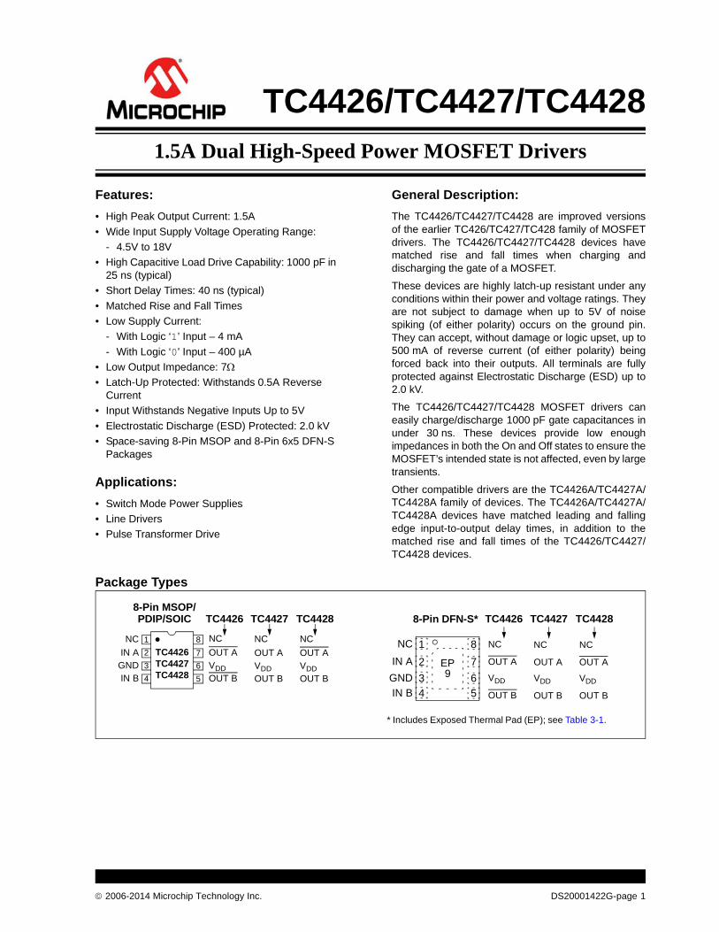
Package Types
1
2
3
4
NC
5
6
7
8
OUT A
OUT B
NC
IN AGNDIN B
VDD
TC4426TC4427
TC4426 TC4427
NC
OUT A
OUT BVDD
TC4428
NC
OUT A
OUT BVDD
TC4428
NC
OUT A
OUT B
VDD
TC4426 TC4427
NC
OUT A
OUT B
VDD
TC4428
NC
OUT A
OUT B
VDD
8-Pin MSOP/PDIP/SOIC
GND
IN A
IN B
1
2
3
4
8
7
6
5
NC
EP9
8-Pin DFN-S*
* Includes Exposed Thermal Pad (EP); see Table 3-1.
1.5A Dual High-Speed Power MOSFET Drivers
TC4426/TC4427/TC4428
DS20001422G-page 2 2006-2014 Microchip Technology Inc.
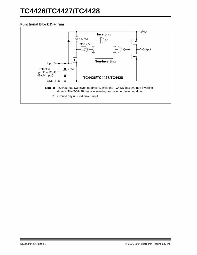
Functional Block Diagram
Effective Input C = 12 pF (Each Input)
TC4426/TC4427/TC4428
Output
Input
GND
VDD
300 mV
4.7V
Inverting
Non-Inverting
Note 1: TC4426 has two inverting drivers, while the TC4427 has two non-invertingdrivers. The TC4428 has one inverting and one non-inverting driver.
2: Ground any unused driver input.
1.5 mA
2006-2014 Microchip Technology Inc. DS20001422G-page 3
TC4426/TC4427/TC4428
1.0 ELECTRICAL CHARACTERISTICS
Absolute Maximum Ratings †
Supply Voltage ................................................................+22V
Input Voltage, IN A or IN B.......... (VDD + 0.3V) to (GND – 5V)
Package Power Dissipation (TA +70°C)DFN-S ..................................................................... Note 3MSOP.....................................................................340 mWPDIP .......................................................................730 mWSOIC.......................................................................470 mW
Storage Temperature Range.........................-65°C to +150°C
Maximum Junction Temperature................................. +150°C
† Stresses above those listed under “Absolute MaximumRatings” may cause permanent damage to the device. Theseare stress ratings only and functional operation of the deviceat these or any other conditions above those indicated in theoperation sections of the specifications is not implied.Exposure to Absolute Maximum Rating conditions forextended periods may affect device reliability.
DC CHARACTERISTICSElectrical Specifications: Unless otherwise noted, TA = +25ºC with 4.5V VDD 18V.
Parameters Sym. Min. Typ. Max. Units Conditions
Input
Logic ‘1’, High Input Voltage VIH 2.4 — — V Note 2
Logic ‘0’, Low Input Voltage VIL — — 0.8 V
Input Current IIN -1.0 — +1.0 µA 0VVINVDD
Output
High Output Voltage VOH VDD – 0.025 — — V DC Test
Low Output Voltage VOL — — 0.025 V DC Test
Output Resistance RO — 7 10 IOUT = 10 mA, VDD = 18V
Peak Output Current IPK — 1.5 — A VDD = 18V
Latch-Up ProtectionWithstand Reverse Current
IREV — > 0.5 — A Duty cycle2%, t 300 µsVDD = 18V
Switching Time (Note 1)
Rise Time tR — 19 30 ns Figure 4-1
Fall Time tF — 19 30 ns Figure 4-1
Delay Time tD1 — 20 30 ns Figure 4-1
Delay Time tD2 — 40 50 ns Figure 4-1
Power Supply
Power Supply Current IS ——
——
4.50.4
mA VIN = 3V (Both inputs)VIN = 0V (Both inputs)
Note 1: Switching times ensured by design.
2: For V temperature range devices, the VIH (Min) limit is 2.0V.
3: Package power dissipation is dependent on the copper pad area on the PCB.
TC4426/TC4427/TC4428
DS20001422G-page 4 2006-2014 Microchip Technology Inc.
DC CHARACTERISTICS (OVER OPERATING TEMPERATURE RANGE)
TEMPERATURE CHARACTERISTICS
Electrical Specifications: Unless otherwise noted, over operating temperature range with 4.5V VDD 18V.
Parameters Sym. Min. Typ. Max. Units Conditions
Input
Logic ‘1’, High Input Voltage VIH 2.4 — — V Note 2
Logic ‘0’, Low Input Voltage VIL — — 0.8 V
Input Current IIN -10 — +10 µA 0VVINVDD
Output
High Output Voltage VOH VDD – 0.025 — — V DC Test
Low Output Voltage VOL — — 0.025 V DC Test
Output Resistance RO — 9 12 IOUT = 10 mA, VDD = 18V
Peak Output Current IPK — 1.5 — A VDD = 18V
Latch-Up ProtectionWithstand Reverse Current
IREV — >0.5 — A Duty cycle2%, t 300 µsVDD = 18V
Switching Time (Note 1)
Rise Time tR — — 40 ns Figure 4-1
Fall Time tF — — 40 ns Figure 4-1
Delay Time tD1 — — 40 ns Figure 4-1
Delay Time tD2 — — 60 ns Figure 4-1
Power Supply
Power Supply Current IS ——
——
8.00.6
mA VIN = 3V (Both inputs)VIN = 0V (Both inputs)
Note 1: Switching times ensured by design.
2: For V temperature range devices, the VIH (Min) limit is 2.0V.
Electrical Specifications: Unless otherwise noted, all parameters apply with 4.5V VDD 18V.
Parameters Sym. Min. Typ. Max. Units Conditions
Temperature Ranges
Specified Temperature Range (C) TA 0 — +70 °C
Specified Temperature Range (E) TA -40 — +85 °C
Specified Temperature Range (V) TA -40 — +125 °C
Maximum Junction Temperature TJ — — +150 °C
Storage Temperature Range TA -65 — +150 °C
Package Thermal Resistances
Thermal Resistance, 8L-6x5 DFN-S JA — 33.2 — °C/W
Thermal Resistance, 8L-MSOP JA — 206 — °C/W
Thermal Resistance, 8L-PDIP JA — 125 — °C/W
Thermal Resistance, 8L-SOIC JA — 155 — °C/W
2006-2014 Microchip Technology Inc. DS20001422G-page 5
TC4426/TC4427/TC4428
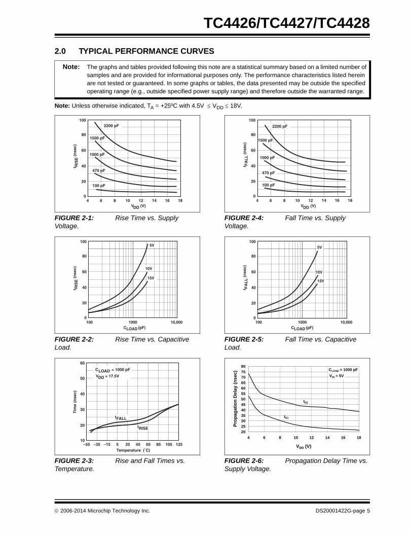
2.0 TYPICAL PERFORMANCE CURVES
Note: Unless otherwise indicated, TA = +25ºC with 4.5V VDD 18V.
FIGURE 2-1: Rise Time vs. Supply Voltage.
FIGURE 2-2: Rise Time vs. Capacitive Load.
FIGURE 2-3: Rise and Fall Times vs. Temperature.
FIGURE 2-4: Fall Time vs. Supply Voltage.
FIGURE 2-5: Fall Time vs. Capacitive Load.
FIGURE 2-6: Propagation Delay Time vs. Supply Voltage.
Note: The graphs and tables provided following this note are a statistical summary based on a limited number of samples and are provided for informational purposes only. The performance characteristics listed herein are not tested or guaranteed. In some graphs or tables, the data presented may be outside the specified operating range (e.g., outside specified power supply range) and therefore outside the warranted range.
t RIS
E (
nse
c)
4 6 8 10 12 14 16 18
100 pF
470 pF
2200 pF
1500 pF
100
1000 pF
80
60
40
20
0
VDD (V)
100 1000 10,000C (pF)LOAD
5V
10V
15V
100
80
60
40
20
0
t RIS
E (
nse
c)T
ime
(nse
c)
tRISE
Temperature (˚C)
C = 1000 pFLOADV = 17.5VDD
60
–55 –35 5 25 45 65 85 105 125–15
tFALL
50
40
30
20
10
t FA
LL
(n
sec)
4 6 8 10 12 14 16 18
100 pF
470 pF
1000 pF
2200 pF
1500 pF
100
80
60
40
20
0
VDD (V)
100 1000 10,000
5V
10V
C (pF)LOAD
100
80
60
40
20
0
t FA
LL
(n
sec)
15V
2025
303540
4550
556065
7075
80
4 6 8 10 12 14 16 18
VDD (V)
Pro
pag
atio
n D
ela
y (n
sec)
tD1
tD2
CLOAD = 1000 pF
VIN = 5V
TC4426/TC4427/TC4428
DS20001422G-page 6 2006-2014 Microchip Technology Inc.
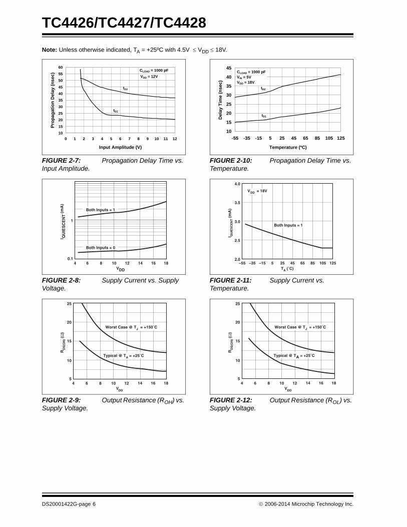
Note: Unless otherwise indicated, TA = +25ºC with 4.5V VDD 18V.
FIGURE 2-7: Propagation Delay Time vs. Input Amplitude.
FIGURE 2-8: Supply Current vs. Supply Voltage.
FIGURE 2-9: Output Resistance (ROH) vs. Supply Voltage.
FIGURE 2-10: Propagation Delay Time vs. Temperature.
FIGURE 2-11: Supply Current vs. Temperature.
FIGURE 2-12: Output Resistance (ROL) vs. Supply Voltage.
10
15
20
25
30
35
40
45
50
55
60
0 1 2 3 4 5 6 7 8 9 10 11 12
Input Amplitude (V)
Pro
pa
gat
ion
Del
ay (
ns
ec)
tD1
tD2
CLOAD = 1000 pF
VDD = 12V
4
I
(
mA
)Q
UIE
SC
EN
T
186 8 10 12 14 160.1
Both Inputs = 1
Both Inputs = 0
V DD
1
4 6 8 10 12 14 16 18V DD
RD
S(O
N) (
Ω)
20
25
15
10
5
Worst Case @ TJ = +150˚C
Typical @ TA = +25˚C
10
15
20
25
30
35
40
45
-55 -35 -15 5 25 45 65 85 105 125
Temperature (ºC)
Del
ay T
ime
(nse
c)
tD1
tD2
CLOAD = 1000 pFVIN = 5VVDD = 18V
TA (˚C)
I QU
IES
CE
NT (
mA
)
4.0
3.5
3.0
2.5
2.0–55 –35 –15 5 25 45 65 85 105 125
V = 18VDD
Both Inputs = 1
4 6 8 10 12 14 16 18
20
V DD
25
15
10
5
Worst Case @ TJ = +150˚C
Typical @ TA = +25˚C
RD
S(O
N) (
Ω)
2006-2014 Microchip Technology Inc. DS20001422G-page 7
TC4426/TC4427/TC4428
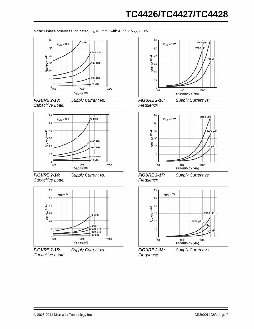
Note: Unless otherwise indicated, TA = +25ºC with 4.5V VDD 18V.
FIGURE 2-13: Supply Current vs. Capacitive Load.
FIGURE 2-14: Supply Current vs. Capacitive Load.
FIGURE 2-15: Supply Current vs. Capacitive Load.
FIGURE 2-16: Supply Current vs. Frequency.
FIGURE 2-17: Supply Current vs. Frequency.
FIGURE 2-18: Supply Current vs. Frequency.
60
100 1000 10,000
I SU
PP
LY
(m
A)
2 MHz
600 kHz
200 kHz
20 kHz
900 kHz
C (pF)LOAD
V = 18VDD50
40
30
20
10
0
100 1000 10,000
2 MHz
600 kHz
200 kHz20 kHz
900 kHz
V = 12VDD
C (pF)LOAD
60
50
40
30
20
10
0
I SU
PP
LY
(m
A)
100 1000 10,000
2 MHz
200 kHz20 kHz
600 kHz900 kHz
V = 6VDD
C (pF)LOAD
60
50
40
30
20
10
0
I SU
PP
LY
(m
A)
10 100 1000FREQUENCY (kHz)
1000 pF
2200 pF
V = 18VDD
100 pF
60
50
40
30
20
10
0
I SU
PP
LY
(m
A)
10 100 1000FREQUENCY (kHz)
1000 pF
2200 pF
100 pF
V = 12VDD
60
50
40
30
20
10
0
I SU
PP
LY
(m
A)
10 100 1000FREQUENCY (kHz)
1000 pF
2200 pF
100 pF
V = 6VDD
60
50
40
30
20
10
0
I SU
PP
LY
(m
A)
TC4426/TC4427/TC4428
DS20001422G-page 8 2006-2014 Microchip Technology Inc.
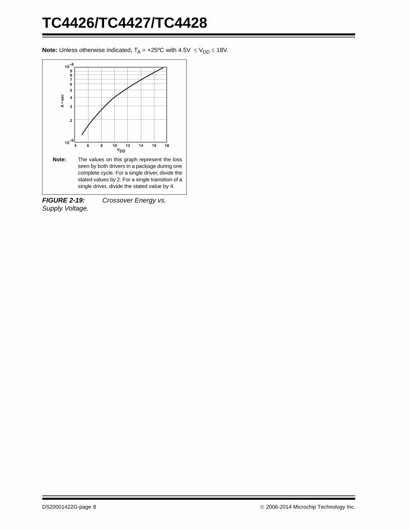
Note: Unless otherwise indicated, TA = +25ºC with 4.5V VDD 18V.
FIGURE 2-19: Crossover Energy vs. Supply Voltage.
4
A •
sec
186 8 10 12 14 16
876
5
4
3
2
10–9
10–8
9
V DD
Note: The values on this graph represent the lossseen by both drivers in a package during onecomplete cycle. For a single driver, divide thestated values by 2. For a single transition of asingle driver, divide the stated value by 4.
2006-2014 Microchip Technology Inc. DS20001422G-page 9
TC4426/TC4427/TC4428
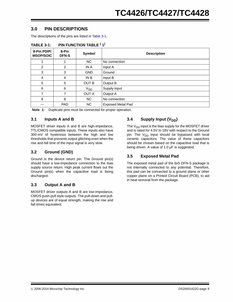
3.0 PIN DESCRIPTIONS
The descriptions of the pins are listed in Table 3-1.
TABLE 3-1: PIN FUNCTION TABLE ( 1)
3.1 Inputs A and B
MOSFET driver inputs A and B are high-impedance,TTL/CMOS compatible inputs. These inputs also have300 mV of hysteresis between the high and lowthresholds that prevents output glitching even when therise and fall time of the input signal is very slow.
3.2 Ground (GND)
Ground is the device return pin. The Ground pin(s)should have a low-impedance connection to the biassupply source return. High peak current flows out theGround pin(s) when the capacitive load is beingdischarged.
3.3 Output A and B
MOSFET driver outputs A and B are low-impedance,CMOS push-pull style outputs. The pull-down and pull-up devices are of equal strength, making the rise andfall times equivalent.
3.4 Supply Input (VDD)
The VDD input is the bias supply for the MOSFET driverand is rated for 4.5V to 18V with respect to the Groundpin. The VDD input should be bypassed with localceramic capacitors. The value of these capacitorsshould be chosen based on the capacitive load that isbeing driven. A value of 1.0 µF is suggested.
3.5 Exposed Metal Pad
The exposed metal pad of the 6x5 DFN-S package isnot internally connected to any potential. Therefore,this pad can be connected to a ground plane or othercopper plane on a Printed Circuit Board (PCB), to aidin heat removal from the package.
8-Pin PDIP/ MSOP/SOIC
8-PinDFN-S
Symbol Description
1 1 NC No connection
2 2 IN A Input A
3 3 GND Ground
4 4 IN B Input B
5 5 OUT B Output B
6 6 VDD Supply input
7 7 OUT A Output A
8 8 NC No connection
— PAD NC Exposed Metal Pad
Note 1: Duplicate pins must be connected for proper operation.
TC4426/TC4427/TC4428
DS20001422G-page 10 2006-2014 Microchip Technology Inc.
4.0 APPLICATIONS INFORMATION
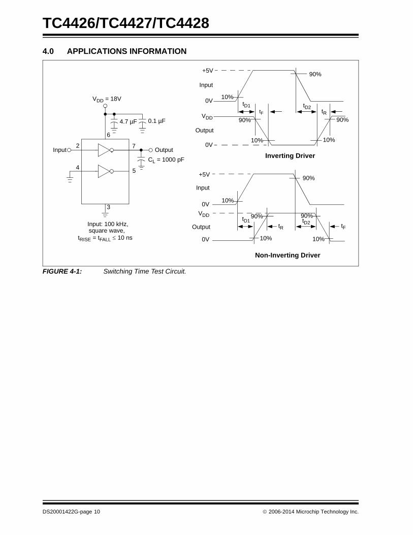
FIGURE 4-1: Switching Time Test Circuit.
CL = 1000 pF
0.1 µF4.7 µF
Inverting Driver
Non-Inverting Driver
Input
VDD = 18V
Input
Output
tD1tF
tR
tD2Input: 100 kHz,square wave,
tRISE = tFALL 10 ns
Output
Input
Output
tD1tF
tR
tD2
+5V
10%
90%
10%
90%
10%
90%VDD
0V
90%
10%
10% 10%
90%
+5V
VDD
0V
0V
0V
90%
3
2 7
6
4 5
2006-2014 Microchip Technology Inc. DS20001422G-page 11
TC4426/TC4427/TC4428
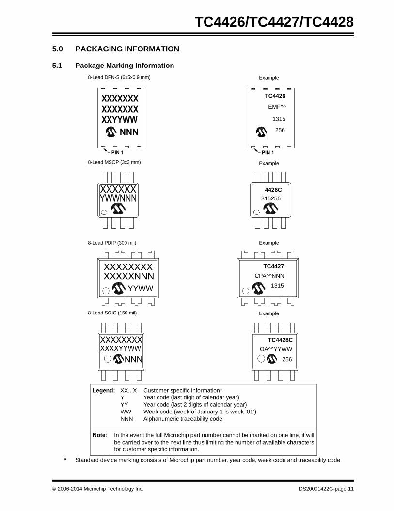
5.0 PACKAGING INFORMATION
5.1 Package Marking Information
PIN 1
NNN
PIN 1
NNN
Legend: XX...X Customer specific information*Y Year code (last digit of calendar year)YY Year code (last 2 digits of calendar year)WW Week code (week of January 1 is week ‘01’)NNN Alphanumeric traceability code
Note: In the event the full Microchip part number cannot be marked on one line, it willbe carried over to the next line thus limiting the number of available charactersfor customer specific information.
* Standard device marking consists of Microchip part number, year code, week code and traceability code.
TC4426
EMF^^
1315
256
4426C
315256
XXXXXXXXXXXXXNNN
YYWW
TC4427
CPA^^NNN
1315
TC4428C
OA^^YYWW
256
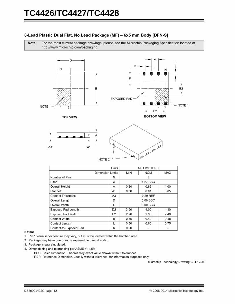
8-Lead DFN-S (6x5x0.9 mm)
8-Lead MSOP (3x3 mm)
8-Lead PDIP (300 mil)
8-Lead SOIC (150 mil) Example
Example
Example
Example
TC4426/TC4427/TC4428
DS20001422G-page 12 2006-2014 Microchip Technology Inc.
���������� ������������������������������������������� �!����"#
�
�����$�� ������ �!"�����# $�% �&"� �'��� ���(�)"&�'"!&�) �����& #�*�&����&� ���&�� #��� ���� ���+�� �'����� ��� ����'�� � $�! #�&� �)��!��&� �#!�,� ���+�� ��!�!�*�!���"��& #��� ��' �!���������#�&�� �������� �����-�.���/��
0�12 0�!�����' �!������� �� &������� $��&� ��" �!��*��*�&��"&�&�� ���� !��-32 � % � �� ���' �!���(�"!"�����*�&��"&�&�� ���� (�%�����%��'�&����"��! !������
����$ 3���&� �'�!&��"�� �&���+�� �#��*���!(�� �! �! �&� �������������+������� ��%���&��������& #��&��&&244***�'����������'4��+�����
5��&! ��66��-�-����' �!����6�'�&! ��7 78� ��9
7"') ���%����! 7 :��&�� �����0�18 �����; ���& � ��:� ��:/ �����&��#�%%� �� ���� ���� ���/1��&��&�����+� !! �, ������-38 �����6 ��&� � /����0�18 �����<�#&� - �����0�1-$�! #���#�6 ��&� �� ,��� ���� ����-$�! #���#�<�#&� -� ���� ��,� ����1��&��&�<�#&� ) ��,/ ���� ���:1��&��&�6 ��&� 6 ��/� ���� ���/1��&��&&�-$�! #���# = ���� > >
NOTE 2
A1
A
A3
NOTE 1 1 2
E
N
D
EXPOSED PAD
NOTE 12 1
E2
L
N
e
b
K
BOTTOM VIEWTOP VIEW
D2
�������� � �������� ���*��� 1�����0
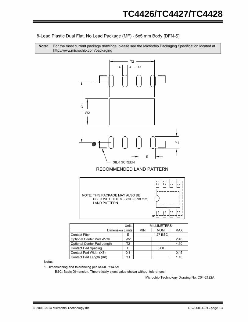
2006-2014 Microchip Technology Inc. DS20001422G-page 13
TC4426/TC4427/TC4428
����$ 3���&� �'�!&��"�� �&���+�� �#��*���!(�� �! �! �&� �������������+������� ��%���&��������& #��&��&&244***�'����������'4��+�����
TC4426/TC4427/TC4428
DS20001422G-page 14 2006-2014 Microchip Technology Inc.
For the most current package drawings, please see the Microchip Packaging Specification located at http://www.microchip.com/packaging
2006-2014 Microchip Technology Inc. DS20001422G-page 15
TC4426/TC4427/TC4428
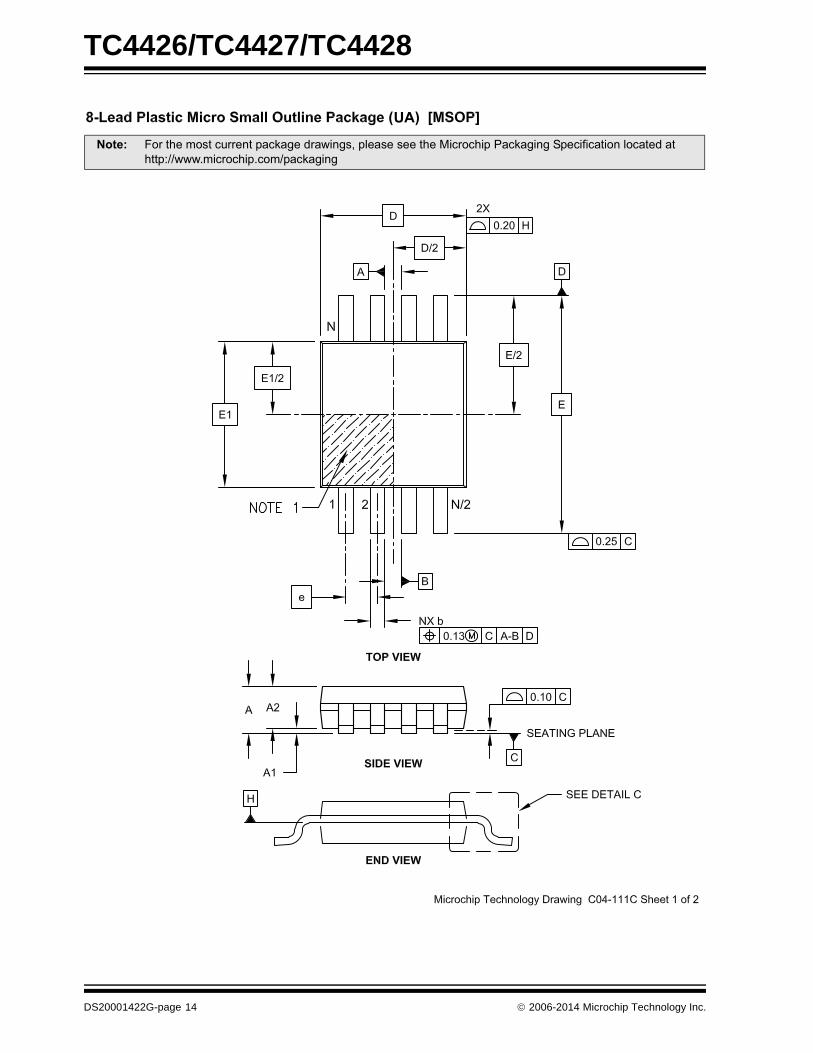
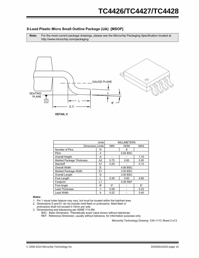
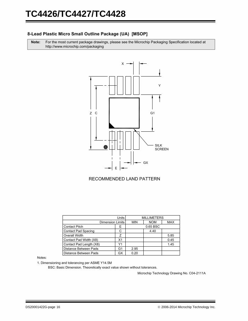
Note: For the most current package drawings, please see the Microchip Packaging Specification located at http://www.microchip.com/packaging
UA
TC4426/TC4427/TC4428
DS20001422G-page 16 2006-2014 Microchip Technology Inc.
8-Lead Plastic Micro Small Outline Package (UA) [MSOP]
Note: For the most current package drawings, please see the Microchip Packaging Specification located at http://www.microchip.com/packaging
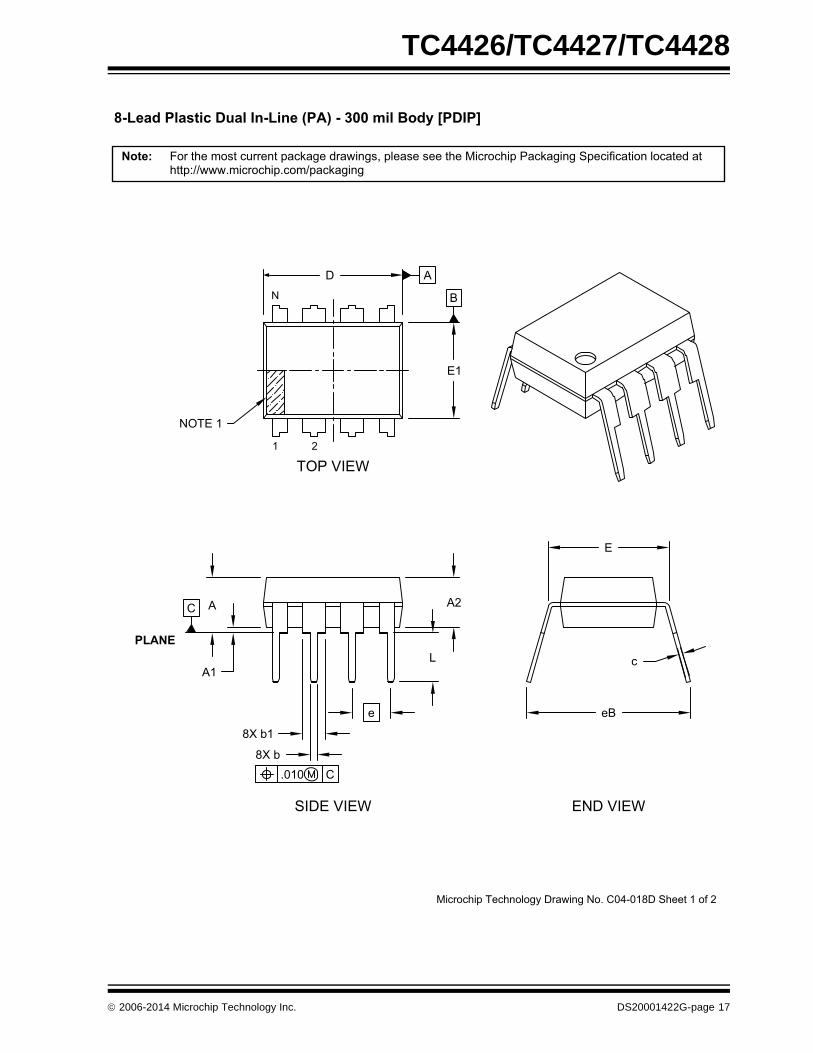
2006-2014 Microchip Technology Inc. DS20001422G-page 17
TC4426/TC4427/TC4428
B
A
For the most current package drawings, please see the Microchip Packaging Specification located athttp://www.microchip.com/packaging
Microchip Technology Drawing No. C04-018D Sheet 1 of 2
eB
E
A
A1
A2
L
8X b
8X b1
D
E1
c
C
.010 C
1 2
N
NOTE 1
TOP VIEW
END VIEWSIDE VIEW
e
TC4426/TC4427/TC4428
DS20001422G-page 18 2006-2014 Microchip Technology Inc.
Microchip Technology Drawing No. C04-018D Sheet 2 of 2
For the most current package drawings, please see the Microchip Packaging Specification located athttp://www.microchip.com/packaging
Units INCHESDimension Limits MIN NOM MAX
Number of Pins N 8Pitch e .100 BSCTop to Seating Plane A - - .210Molded Package Thickness A2 .115 .130 .195Base to Seating Plane A1 .015Shoulder to Shoulder Width E .290 .310 .325Molded Package Width E1 .240 .250 .280Overall Length D .348 .365 .400Tip to Seating Plane L .115 .130 .150Lead Thickness c .008 .010 .015Upper Lead Width b1 .040 .060 .070Lower Lead Width b .014 .018 .022Overall Row Spacing eB - - .430
BSC: Basic Dimension. Theoretically exact value shown without tolerances.
3.
1.
protrusions shall not exceed .010" per side.
2.
4.
Notes:
§
- -
Dimensions D and E1 do not include mold flash or protrusions. Mold flash or
Pin 1 visual index feature may vary, but must be located within the hatched area.§ Significant Characteristic
Dimensioning and tolerancing per ASME Y14.5M
e
DATUM A DATUM A
e
be2
be2
ALTERNATE LEAD DESIGN(VENDOR DEPENDENT)
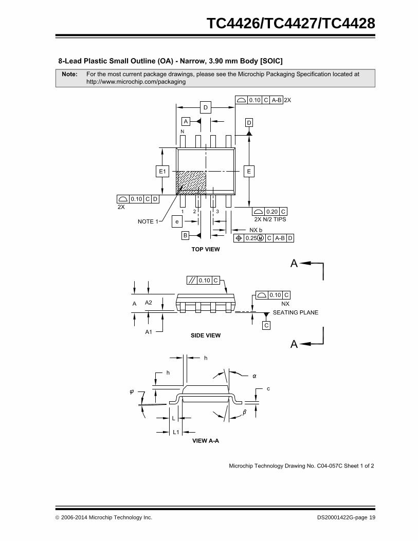
2006-2014 Microchip Technology Inc. DS20001422G-page 19
TC4426/TC4427/TC4428
Note: For the most current package drawings, please see the Microchip Packaging Specification located at http://www.microchip.com/packaging
TC4426/TC4427/TC4428
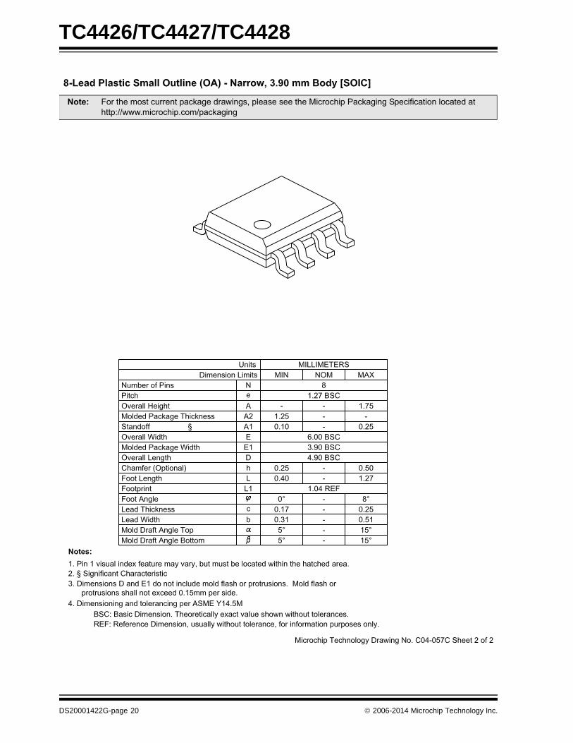
DS20001422G-page 20 2006-2014 Microchip Technology Inc.
Note: For the most current package drawings, please see the Microchip Packaging Specification located at http://www.microchip.com/packaging
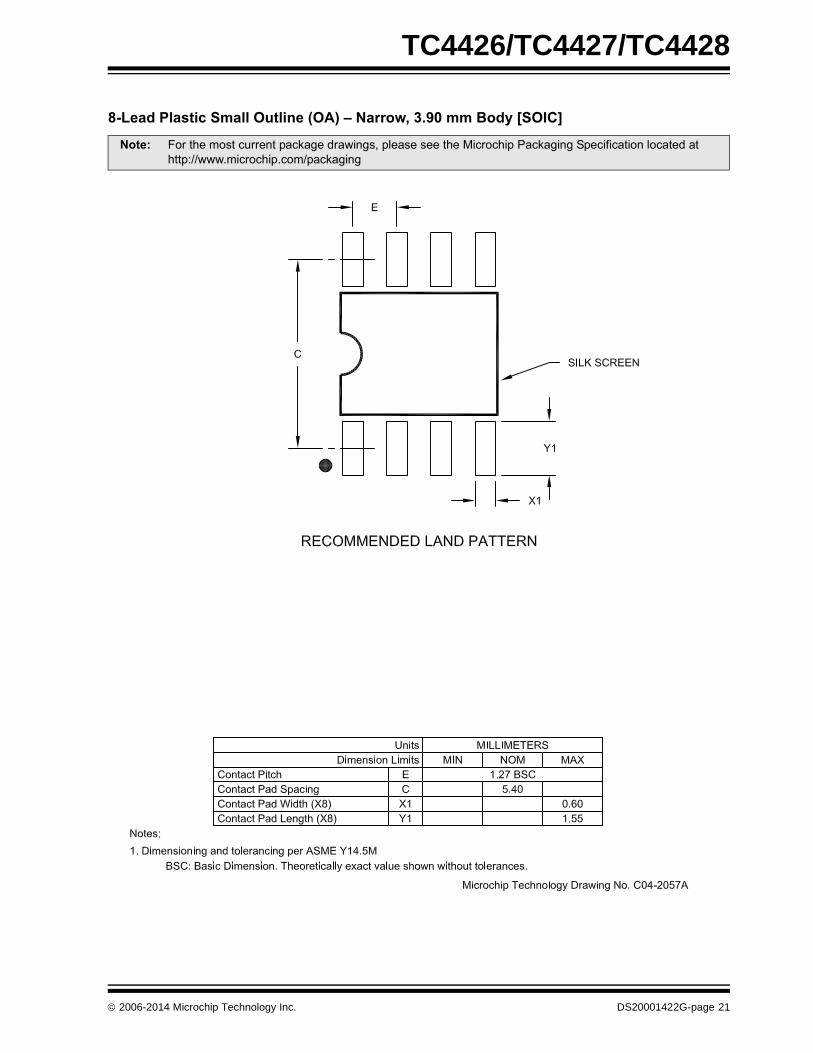
2006-2014 Microchip Technology Inc. DS20001422G-page 21
TC4426/TC4427/TC4428
���������� ��"���%�� &���%'������((�)��*+,-������� �!"%./#
����$ 3���&� �'�!&��"�� �&���+�� �#��*���!(�� �! �! �&� �������������+������� ��%���&��������& #��&��&&244***�'����������'4��+�����

TC4426/TC4427/TC4428
DS20001422G-page 22 2006-2014 Microchip Technology Inc.
NOTES:
2006-2014 Microchip Technology Inc. DS20001422G-page 23
TC4426/TC4427/TC4428
APPENDIX A: REVISION HISTORY
Revision G (July 2014)
The following is the list of modifications:
1. Updated the Functional Block Diagram.
Revision F (September 2013)
The following is the list of modifications:
2. Updated the Electrostatic Discharge (ESD)rating to 2kV in the Features section.
3. Updated the package drawings in Section 5.0“Packaging Information”.
4. Minor typographical and editorial corrections.
Revisions E (December 2012)
• Added a note to each package outline drawing.
TC4426/TC4427/TC4428
DS20001422G-page 24 2006-2014 Microchip Technology Inc.
NOTES:
2006-2014 Microchip Technology Inc. DS20001422G-page 25
TC4426/TC4427/TC4428
PRODUCT IDENTIFICATION SYSTEM
To order or obtain information, e.g., on pricing or delivery, refer to the factory or the listed sales office.
Device: TC4426: 1.5A Dual MOSFET Driver, InvertingTC4427: 1.5A Dual MOSFET Driver, Non-InvertingTC4428: 1.5A Dual MOSFET Driver, Complementary
Temperature Range: C = 0°C to +70°C (PDIP and SOIC only)E = -40°C to +85°CV = -40°C to +125°C
Package: MF = Dual, Flat, No-Lead (6X5 mm Body), 8-leadMF713 = Dual, Flat, No-Lead (6X5 mm Body), 8-lead
(Tape and Reel)OA = Plastic SOIC, (150 mil Body), 8-leadOA713 = Plastic SOIC, (150 mil Body), 8-lead
(Tape and Reel)PA = Plastic DIP (300 mil Body), 8-leadUA = Plastic Micro Small Outline (MSOP), 8-leadUA713 = Plastic Micro Small Outline (MSOP), 8-lead
(Tape and Reel)
Examples:
a) TC4426COA: 1.5A Dual InvertingMOSFET driver,0°C to +70°CSOIC package.
b) TC4426EUA: 1.5A Dual InvertingMOSFET driver,-40°C to +85°C.MSOP package.
c) TC4426EMF: 1.5A Dual InvertingMOSFET driver,-40°C to +85°C,DFN-S package.
a) TC4427CPA: 1.5A Dual Non-InvertingMOSFET driver,0°C to +70°CPDIP package.
b) TC4427EPA: 1.5A Dual Non-InvertingMOSFET driver,-40°C to +85°CPDIP package.
a) TC4428COA713:1.5A Dual ComplementaryMOSFET driver,0°C to +70°C,SOIC package,Tape and Reel.
b) TC4428EMF: 1.5A Dual Complementary,MOSFET driver,-40°C to +85°CDFN-S package.
PART NO. X XX
PackageTemperatureRange
Device
XXX
Tape & Reel
X
PB Free

TC4426/TC4427/TC4428
DS20001422G-page 26 2006-2014 Microchip Technology Inc.
NOTES:
2006-2014 Microchip Technology Inc. DS20001422G-page 27
Information contained in this publication regarding deviceapplications and the like is provided only for your convenienceand may be superseded by updates. It is your responsibility toensure that your application meets with your specifications.MICROCHIP MAKES NO REPRESENTATIONS ORWARRANTIES OF ANY KIND WHETHER EXPRESS ORIMPLIED, WRITTEN OR ORAL, STATUTORY OROTHERWISE, RELATED TO THE INFORMATION,INCLUDING BUT NOT LIMITED TO ITS CONDITION,QUALITY, PERFORMANCE, MERCHANTABILITY ORFITNESS FOR PURPOSE. Microchip disclaims all liabilityarising from this information and its use. Use of Microchipdevices in life support and/or safety applications is entirely atthe buyer’s risk, and the buyer agrees to defend, indemnify andhold harmless Microchip from any and all damages, claims,suits, or expenses resulting from such use. No licenses areconveyed, implicitly or otherwise, under any Microchipintellectual property rights.
Trademarks
The Microchip name and logo, the Microchip logo, dsPIC, FlashFlex, flexPWR, JukeBlox, KEELOQ, KEELOQ logo, Kleer, LANCheck, MediaLB, MOST, MOST logo, MPLAB, OptoLyzer, PIC, PICSTART, PIC32 logo, RightTouch, SpyNIC, SST, SST Logo, SuperFlash and UNI/O are registered trademarks of Microchip Technology Incorporated in the U.S.A. and other countries.
The Embedded Control Solutions Company and mTouch are registered trademarks of Microchip Technology Incorporated in the U.S.A.
Analog-for-the-Digital Age, BodyCom, chipKIT, chipKIT logo, CodeGuard, dsPICDEM, dsPICDEM.net, ECAN, In-Circuit Serial Programming, ICSP, Inter-Chip Connectivity, KleerNet, KleerNet logo, MiWi, MPASM, MPF, MPLAB Certified logo, MPLIB, MPLINK, MultiTRAK, NetDetach, Omniscient Code Generation, PICDEM, PICDEM.net, PICkit, PICtail, RightTouch logo, REAL ICE, SQI, Serial Quad I/O, Total Endurance, TSHARC, USBCheck, VariSense, ViewSpan, WiperLock, Wireless DNA, and ZENA are trademarks of Microchip Technology Incorporated in the U.S.A. and other countries.
SQTP is a service mark of Microchip Technology Incorporated in the U.S.A.
Silicon Storage Technology is a registered trademark of Microchip Technology Inc. in other countries.
GestIC is a registered trademarks of Microchip Technology Germany II GmbH & Co. KG, a subsidiary of Microchip Technology Inc., in other countries.
All other trademarks mentioned herein are property of their respective companies.
© 2006-2014, Microchip Technology Incorporated, Printed in the U.S.A., All Rights Reserved.
ISBN:978-1-63276-371-6
Note the following details of the code protection feature on Microchip devices:
• Microchip products meet the specification contained in their particular Microchip Data Sheet.
• Microchip believes that its family of products is one of the most secure families of its kind on the market today, when used in the intended manner and under normal conditions.
• There are dishonest and possibly illegal methods used to breach the code protection feature. All of these methods, to our knowledge, require using the Microchip products in a manner outside the operating specifications contained in Microchip’s Data Sheets. Most likely, the person doing so is engaged in theft of intellectual property.
• Microchip is willing to work with the customer who is concerned about the integrity of their code.
• Neither Microchip nor any other semiconductor manufacturer can guarantee the security of their code. Code protection does not mean that we are guaranteeing the product as “unbreakable.”
Code protection is constantly evolving. We at Microchip are committed to continuously improving the code protection features of ourproducts. Attempts to break Microchip’s code protection feature may be a violation of the Digital Millennium Copyright Act. If such actsallow unauthorized access to your software or other copyrighted work, you may have a right to sue for relief under that Act.
Microchip received ISO/TS-16949:2009 certification for its worldwide headquarters, design and wafer fabrication facilities in Chandler and Tempe, Arizona; Gresham, Oregon and design centers in California and India. The Company’s quality system processes and procedures are for its PIC® MCUs and dsPIC® DSCs, KEELOQ® code hopping devices, Serial EEPROMs, microperipherals, nonvolatile memory and analog products. In addition, Microchip’s quality system for the design and manufacture of development systems is ISO 9001:2000 certified.
QUALITY MANAGEMENT SYSTEM CERTIFIED BY DNV
== ISO/TS 16949 ==
DS20001422G-page 28 2006-2014 Microchip Technology Inc.
AMERICASCorporate Office2355 West Chandler Blvd.Chandler, AZ 85224-6199Tel: 480-792-7200 Fax: 480-792-7277Technical Support: http://www.microchip.com/supportWeb Address: www.microchip.com
AtlantaDuluth, GA Tel: 678-957-9614 Fax: 678-957-1455
Austin, TXTel: 512-257-3370
BostonWestborough, MA Tel: 774-760-0087 Fax: 774-760-0088
ChicagoItasca, IL Tel: 630-285-0071 Fax: 630-285-0075
ClevelandIndependence, OH Tel: 216-447-0464 Fax: 216-447-0643
DallasAddison, TX Tel: 972-818-7423 Fax: 972-818-2924
DetroitNovi, MI Tel: 248-848-4000
Houston, TX Tel: 281-894-5983
IndianapolisNoblesville, IN Tel: 317-773-8323Fax: 317-773-5453
Los AngelesMission Viejo, CA Tel: 949-462-9523 Fax: 949-462-9608
New York, NY Tel: 631-435-6000
San Jose, CA Tel: 408-735-9110
Canada - TorontoTel: 905-673-0699 Fax: 905-673-6509
ASIA/PACIFICAsia Pacific OfficeSuites 3707-14, 37th FloorTower 6, The GatewayHarbour City, KowloonHong KongTel: 852-2943-5100Fax: 852-2401-3431
Australia - SydneyTel: 61-2-9868-6733Fax: 61-2-9868-6755
China - BeijingTel: 86-10-8569-7000 Fax: 86-10-8528-2104
China - ChengduTel: 86-28-8665-5511Fax: 86-28-8665-7889
China - ChongqingTel: 86-23-8980-9588Fax: 86-23-8980-9500
China - HangzhouTel: 86-571-8792-8115 Fax: 86-571-8792-8116
China - Hong Kong SARTel: 852-2943-5100 Fax: 852-2401-3431
China - NanjingTel: 86-25-8473-2460Fax: 86-25-8473-2470
China - QingdaoTel: 86-532-8502-7355Fax: 86-532-8502-7205
China - ShanghaiTel: 86-21-5407-5533 Fax: 86-21-5407-5066
China - ShenyangTel: 86-24-2334-2829Fax: 86-24-2334-2393
China - ShenzhenTel: 86-755-8864-2200 Fax: 86-755-8203-1760
China - WuhanTel: 86-27-5980-5300Fax: 86-27-5980-5118
China - XianTel: 86-29-8833-7252Fax: 86-29-8833-7256
China - XiamenTel: 86-592-2388138 Fax: 86-592-2388130
China - ZhuhaiTel: 86-756-3210040 Fax: 86-756-3210049
ASIA/PACIFICIndia - BangaloreTel: 91-80-3090-4444 Fax: 91-80-3090-4123
India - New DelhiTel: 91-11-4160-8631Fax: 91-11-4160-8632
India - PuneTel: 91-20-3019-1500
Japan - OsakaTel: 81-6-6152-7160 Fax: 81-6-6152-9310
Japan - TokyoTel: 81-3-6880- 3770 Fax: 81-3-6880-3771
Korea - DaeguTel: 82-53-744-4301Fax: 82-53-744-4302
Korea - SeoulTel: 82-2-554-7200Fax: 82-2-558-5932 or 82-2-558-5934
Malaysia - Kuala LumpurTel: 60-3-6201-9857Fax: 60-3-6201-9859
Malaysia - PenangTel: 60-4-227-8870Fax: 60-4-227-4068
Philippines - ManilaTel: 63-2-634-9065Fax: 63-2-634-9069
SingaporeTel: 65-6334-8870Fax: 65-6334-8850
Taiwan - Hsin ChuTel: 886-3-5778-366Fax: 886-3-5770-955
Taiwan - KaohsiungTel: 886-7-213-7830
Taiwan - TaipeiTel: 886-2-2508-8600 Fax: 886-2-2508-0102
Thailand - BangkokTel: 66-2-694-1351Fax: 66-2-694-1350
EUROPEAustria - WelsTel: 43-7242-2244-39Fax: 43-7242-2244-393Denmark - CopenhagenTel: 45-4450-2828 Fax: 45-4485-2829
France - ParisTel: 33-1-69-53-63-20 Fax: 33-1-69-30-90-79
Germany - DusseldorfTel: 49-2129-3766400
Germany - MunichTel: 49-89-627-144-0 Fax: 49-89-627-144-44
Germany - PforzheimTel: 49-7231-424750
Italy - Milan Tel: 39-0331-742611 Fax: 39-0331-466781
Italy - VeniceTel: 39-049-7625286
Netherlands - DrunenTel: 31-416-690399 Fax: 31-416-690340
Poland - WarsawTel: 48-22-3325737
Spain - MadridTel: 34-91-708-08-90Fax: 34-91-708-08-91
Sweden - StockholmTel: 46-8-5090-4654
UK - WokinghamTel: 44-118-921-5800Fax: 44-118-921-5820
Worldwide Sales and Service
03/25/14