Embed Size (px)
Citation preview
MENU
(/)
MANUFACTURING & PROCESS TECHNOLOGY (/CATEGORY-MAIN-PAGE-MANUFACTURING/)
200mm Fab CrunchShortages of used equipment and lower margins mean this problem isn’t getting solved anytime soon.
Growing demand for analog, MEMS and RF chips continues to cause acute
shortages for both 200mm fab capacity and equipment, and it shows no sign of
letting up.
Today, 200mm fab capacity is tight with a similar situation projected for the
second half of 2018 and perhaps well into 2019. In fact, 2018 will likely represent
the third consecutive year that 200mm fab capacity will be tight. The same holds
true for 200mm equipment.
While the demand picture appears to be a bright spot for the industry, the
situation is causing angst for many customers on several fronts. The 200mm
market doesn’t involve leading-edge chips produced in 300mm fabs, but rather
200mm encompasses a huge number of devices made in older 200mm fabs at
mature nodes. These products include consumer devices, communications ICs
and sensors.
11
MAY 21ST, 2018 - BY: MARK LAPEDUS(HTTPS://SEMIENGINEERING.COM/AUTHOR/MARK-LAPEDUS/)
Page 1 of 16Semiconductor Engineering .:. 200mm Fab Crunch
5/21/2018https://semiengineering.com/200mm-fab-crunch/
In 200mm, there are a number of complicated dynamics. Among them:
• IDMs and fabless design houses hope to meet demand for chips made in
200mm fabs. Yet it’s unclear if vendors can meet all demand, as worldwide
200mm fab capacity is expected to remain tight now and into the future.
• In response, GlobalFoundries
(https://semiengineering.com/entities/globalfoundries/), Samsung
(https://semiengineering.com/entities/samsung-foundry/), SMIC
(https://semiengineering.com/entities/smic/), TowerJazz
(https://semiengineering.com/entities/towerjazz/), TSMC
(https://semiengineering.com/entities/tsmc/), UMC and others are
scrambling to add or find 200mm capacity. Meanwhile, SkyWater
Technology, a new foundry vendor, has entered the 200mm fray.
• Even if there is 200mm capacity available, the industry is stuck as it is
unable to find enough suitable 200mm fab equipment in the market.
• Then, unable to secure enough 200mm capacity or equipment, some
chipmakers are re-thinking their plans about building new 200mm fabs.
Instead, they may build 300mm plants.
This is a complex, anxiety-ridden situation for all parties. “We are seeing that
200mm remains oversubscribed. It’s challenging to find any additional capacity
and upside,” said Walter Ng, vice president of business management at UMC
(https://semiengineering.com/entities/umc/). “This used to be a cyclical thing. It
has now become the new norm with 200mm being fully allocated. That’s
something we and others in the industry believe is going to be this way moving
forward. It’s not a UMC-specific situation. This is an industry-wide situation.”
Amazingly, 200mm fabs are expected to remain viable at least until 2030 or so.
As before, the challenge is to procure 200mm equipment, which is still in short
supply.
In fact, 200mm equipment demand has been robust for some time, although
some see a slight pause in the second half of 2018 as chipmakers weigh their
200mm fab plans. Geopolitical issues are also a factor. “200mm capacity
Page 2 of 16Semiconductor Engineering .:. 200mm Fab Crunch
5/21/2018https://semiengineering.com/200mm-fab-crunch/
continues to be tight,” said Joanne Itow, managing director of manufacturing at
Semico Research. “The interesting thing is that demand for 200mm used
equipment has subsided a bit.”
200mm fab boom
The IC market is divided into several segments. At the leading edge, chipmakers
are ramping up chips at 16nm/14nm and beyond in 300mm fabs. In 300mm
fabs, chipmakers also produce chips in several segments above 16nm/14nm.
Both 300mm segments are expanding. “In addition to the logic capacity being
added by the foundries, a significant amount of 300mm capacity is being added
in Korea and China for memory production,” said Adrienne Downey, an analyst at
Semico Research.
But not all chips require advanced nodes. Analog, MEMS, RF and others are
produced in fabs with wafer sizes at 200mm and smaller. For many of these
devices, though, 200mm is a sweet spot.
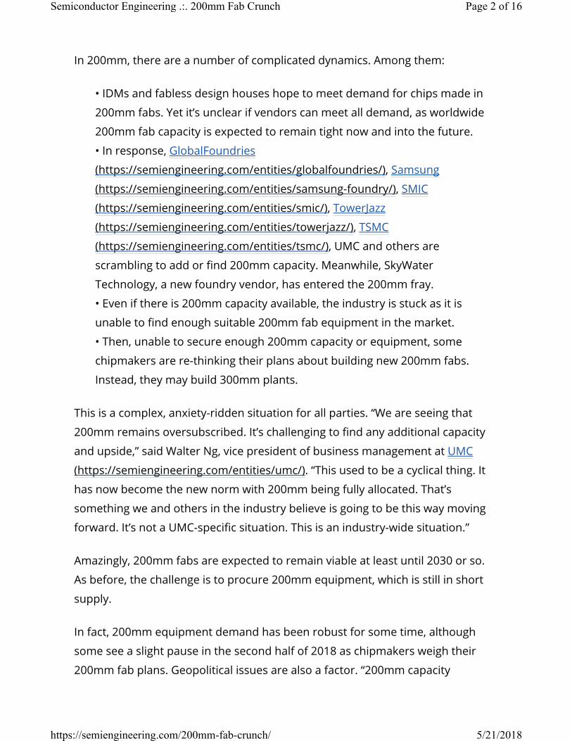
The first 200mm fab appeared in 1990, and the wafer size became the standard
for years. Over time, 200mm was supposed to dwindle as chipmakers began to
migrate to more advanced 300mm fabs in the 2000s. By 2007, 200mm reached
its peak and the market began to decline.
(https://semiengineering.com/wp-content/uploads/2018/05/200fig1.png)
Fig. 1: Relative Difference in Wafer Sizes Source: ICE
(http://smithsonianchips.si.edu/ice/cd/CEICM/SECTION7.pdf)
Page 3 of 16Semiconductor Engineering .:. 200mm Fab Crunch
5/21/2018https://semiengineering.com/200mm-fab-crunch/
In late 2015, though, the industry saw unexpected demand for chips made in
200mm fabs. This overwhelmed the IC supply chain, causing shortages of
200mm fab capacity in 2016 and 2017. And entering into 2018, 200mm capacity
remained tight with no end in sight.
Still, demand for 200mm has taken the industry by surprise and forced
chipmakers and fab tool vendors to take the technology more seriously. For
example, foundries added more 200mm capacity with new and improved
processes. And then, several fab tool vendors began to build new 200mm
equipment.
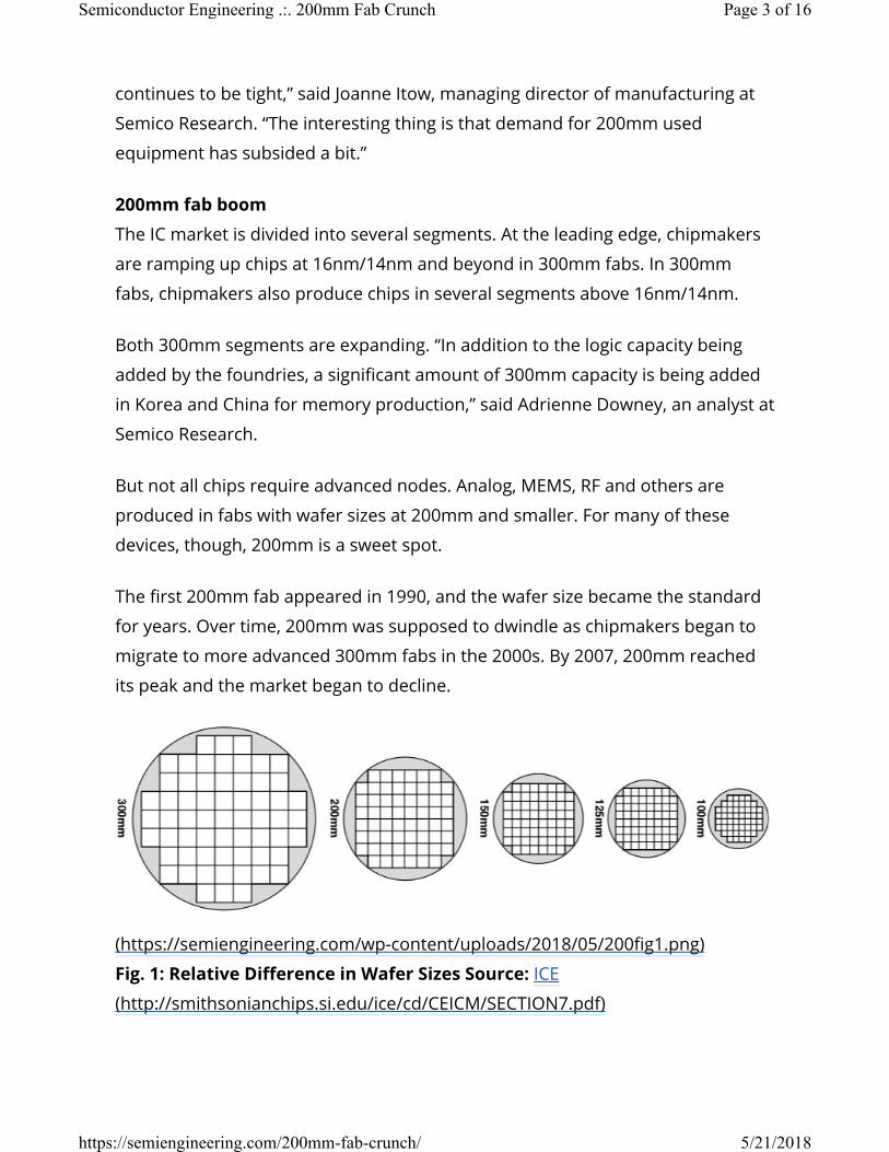
In total, the number of 200mm fabs in production is expected to increase from
188 in 2016 to 202 by 2021, according to Christian Gregor Dieseldorff, an analyst
at SEMI (https://semiengineering.com/entities/semi/). The figure includes IDMs
and foundries.
(https://semiengineering.com/wp-content/uploads/2018/05/200mmfabs.png)
Fig. 2: Growth in the number of 200mm fabs. Source: SEMI
Page 4 of 16Semiconductor Engineering .:. 200mm Fab Crunch
5/21/2018https://semiengineering.com/200mm-fab-crunch/
China is building most of the new 200mm fabs. “We are currently following four
200mm fabs, which are in construction in China. These are for foundry, power
and MEMS,” Dieseldorff said. “Two more were announced (MEMS and power IC).
We expect construction of those fabs to start about the end of this year and
about end of next year.”
A typical 200mm fab produces about 40,000 wafer starts per month. These
plants make wafers at various nodes, ranging from 6-micron to 65nm. “There is a
lot of activity at 180nm/130nm/110nm. It depends on a certain application,”
UMC’s Ng said. “RF, particularly RF SOI, is driving a lot of capacity growth. Power
is also included. You also have things like BCD.”
In 200mm, the applications are exploding. “We are seeing a broadening
application space,” said Mike Rosa, director of strategy and technical marketing
for Applied Materials (https://semiengineering.com/entities/applied-materials-
inc/)‘ 200mm Equipment Product Group. “You have electric vehicles and ADAS.
You have smartphones constantly adding new capabilities.”
Amid the demand for these devices, 200mm fab utilization rates range from the
“high-80 to the low-to-mid 90 percentage range,” with some reporting 100%
today, according to Rosa.
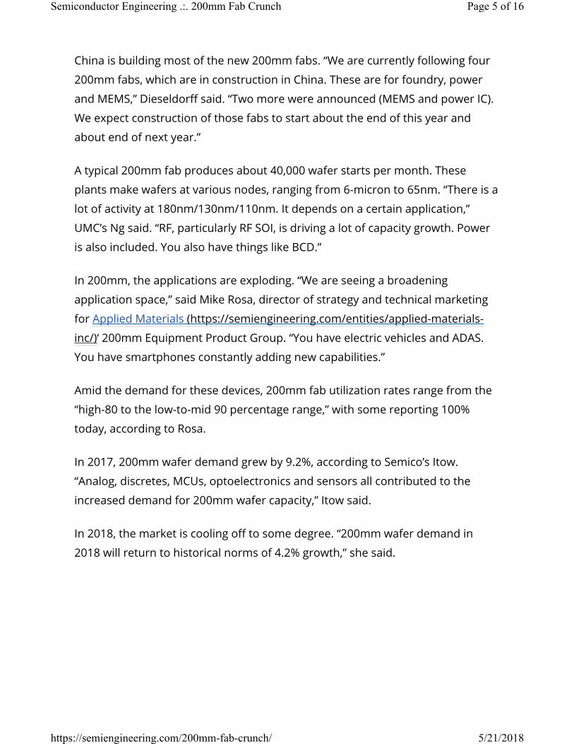
In 2017, 200mm wafer demand grew by 9.2%, according to Semico’s Itow.
“Analog, discretes, MCUs, optoelectronics and sensors all contributed to the
increased demand for 200mm wafer capacity,” Itow said.
In 2018, the market is cooling off to some degree. “200mm wafer demand in
2018 will return to historical norms of 4.2% growth,” she said.
Page 5 of 16Semiconductor Engineering .:. 200mm Fab Crunch
5/21/2018https://semiengineering.com/200mm-fab-crunch/
(https://semiengineering.com/wp-content/uploads/2018/05/200fig3.png)
Fig. 3: 200mm wafer demand by product category, 2018. Source: Semico
Research
One reason for the cooling off period is that fab capacity is tight and
manufacturers are unable to expand. Plus, even if device makers want to
expand, there is a dearth of equipment.
Still, 200mm fab capacity is expected to remain tight for some time, especially at
the foundries. “200mm in the industry is overbooked,” said Bami Bastani, senior
vice president of the RF Business Unit at GlobalFoundries. “A lot of things don’t
need advanced nodes.”
Page 6 of 16Semiconductor Engineering .:. 200mm Fab Crunch
5/21/2018https://semiengineering.com/200mm-fab-crunch/
For example, a smartphone incorporates leading-edge chips, but that represents
a small percentage of the devices. “The rest of it is PMICs, analog and BCD class
of technologies,” Bastani said. “You don’t want to go to smaller geometries with
many of these products. Until they are at the end of life, customers don’t want to
move off of them.”
Generally, customers are happy in terms of having these devices produced in
inexpensive 200mm fabs. But there isn’t enough 200mm capacity, and the
margins are lower than 300mm.
This presents several challenges for foundries. First, vendors must continue to
invest and upgrade the various processes in 200mm. One example is
automotive, where customers want an updated process even if it’s built in
200mm. “The industry needs to continue to invest in new technologies. It seems
like we can’t develop those technologies fast enough,” Applied’s Rosa said.
Besides investing in new 200mm processes, foundries must also find a way to
add 200mm capacity. Here are some options:
• Acquire a company with 200mm fabs.
• Build new 200mm fabs.
• Add more 200mm capacity.
• Move customers from 200mm to 300mm.
• Build a 300mm fab instead.
Going the acquisition route is one idea. Over the years, foundries have acquired
companies to gain access to technology and capacity. But it’s an expensive
option. “Anybody who has an 8-inch fab and is considering selling is putting a
good premium on it,” UMC’s Ng said.
Another option is to build a new 200mm fab. The challenge is to equip the facility
and obtain a return over the long run. “If you are going to invest in putting in
place more capacity, the question is does it make business sense,” Ng said.
Page 7 of 16Semiconductor Engineering .:. 200mm Fab Crunch
5/21/2018https://semiengineering.com/200mm-fab-crunch/
“There are a lot of applications driving the capacity growth in 200mm. Cost is an
important part of it. You can support the capacity growth. But if it’s not at a cost-
effective point, it’s not going to meet the requirements.”
Instead of going these routes, many foundries are moving some chips from
200mm to 300mm. That makes sense for some but not all products. “We are
trying to find solutions for customers on 200mm. We believe part of that will be
moving some of those customers into a 300mm platform where it makes sense,”
he said.
For some chips, it doesn’t make sense to migrate them to 300mm. “A lot of the
applications on 200mm are very cost sensitive. So, it makes it a challenge to do
much of anything,” he said. “For example, some of the power discrete stuff just
never moves.”
Then, with all of the issues in 200mm, some are even re-thinking their 200mm
fab plans. They are even mulling plans to build a 300mm plant, which is also an
expensive option. “If you look at 300mm, your facility costs increase,” Applied’s
Rosa said. “That’s before you even start to consider the availability and readiness
of the technology you might need.”
Meanwhile, foundry customers also face some challenges. Besides securing
enough capacity from their suppliers, customers must evaluate the foundry
landscape. Each foundry is different and each one offers various capabilities.
Plus, there are some new players in the arena. Last year, SkyWater acquired
Cypress Semiconductor’s 200mm fab in Bloomington, Minn. Previously, Cypress’
fab in Bloomington provided foundry services.
With the acquisition of this fab, SkyWater offers foundry services with a twist. It
positions itself as a specialty foundry, with CMOS processes as well as
technologies for biotech, silicon photonics, quantum computing and
superconducting.
Page 8 of 16Semiconductor Engineering .:. 200mm Fab Crunch
5/21/2018https://semiengineering.com/200mm-fab-crunch/
SkyWater has one 200mm fab with 0.35-micron, 90nm and other processes. “If
you look at some foundries, they have very high volumes but they don’t like
customization. The ability to customize is something that you pay a lot of money
for. And depending upon your size, they may not be interested,” said Thomas
Sonderman, president of SkyWater.
“We have the ability to do development in a high-volume environment. One of
the things that the fab mastered when Cypress owned it is the ability to do a high
mix of products with lower volumes and still have world-class yields,” Sonderman
said. “With our model, we can provide the right kinds of volumes for customers
at very competitive prices. But we do in a way where we provide ASIC capability
and specialty technology capacity.”
Wanted: 200mm gear
Meanwhile, IDMs and foundries want to expand their 200mm capacities. So
where can you buy 200mm equipment?
Chipmakers can buy used gear from fab equipment makers, used equipment
companies, brokers, or through online sites such as eBay. Some chipmakers also
sell used equipment on the open market.
In recent times Applied Materials, ASML, KLA-Tencor, Lam Research, TEL and
other equipment makers have been making new 200mm equipment.
At the start of 2018, the industry required around 2,000 new or refurbished
200mm tools to meet fab demand, according to SurplusGlobal, a supplier of
secondary equipment. At the start of 2018, though, there were only 500 available
200mm tools on the market, according to SurplusGlobal.
“We still believe this to be true. We continue to see 200mm demand that is not
met,” said Emerald Greig, executive vice president for the Americas & Europe at
SurplusGlobal. “IDMs and China are definitely driving this, even though we see
demand in the U.S. and Europe, as well.”
Page 9 of 16Semiconductor Engineering .:. 200mm Fab Crunch
5/21/2018https://semiengineering.com/200mm-fab-crunch/
What’s different about this cycle is that the 200mm equipment demand picture
looks uncertain in the second half of 2018. “We see a slight slowdown towards
the second half of the year due to geopolitical factors,” Greig said “We see a
pause in the market due to re-evaluation of installing 200mm or 300mm
equipment.”
Others are more upbeat. “The market is really strong,” Applied’s Rosa said. “In
200mm, we are on track to have at least our strongest year ever.”
Regardless of the short-term outlook, 200mm is expected to remain viable for
some time, so fab managers must procure equipment and spares to meet
demand. Buying 200mm tools from a vendor boils down to several
factors—quality, reputation and service. Even then, there are challenges buying
gear, whether it’s from an OEM, used equipment vendor or elsewhere.
“The cores on the used market can be in every state. On one end of the
spectrum, it can be pristine. The other end can be classified ‘as is,’ and there is
everything in between,” Rosa said. “Then, we’re seeing the availability of 200mm
platforms drying up. What does that do? That increases the lead times. That
forces prices up for used equipment.”
Not all suppliers of 200mm gear are alike. Some offer new tools, while others
refurbish existing ones. There are even cases of firms that sell systems that are
sub-standard or simply don’t work.
“There are two buckets of tool requirements. There are pure capacity-add tools.
If it’s just a capacity add, it’s going to be straightforward,” Rosa said. “If it’s a
capacity add that requires new technology, then this you will not find this on the
second-hand market.”
At Applied, meanwhile, the fab tool vendor builds new 200mm equipment and
also refurbishes them in various segments. Typically, it’s a build-to-order
business with lead times ranging from 12 to 16 weeks.
Page 10 of 16Semiconductor Engineering .:. 200mm Fab Crunch
5/21/2018https://semiengineering.com/200mm-fab-crunch/
In some cases, Applied will build a new 200mm tool from scratch. “That increases
the lead time and price,” he said “We are seeing tool ASPs approaching what they
were when Applied only did 200mm.”
Others also see growth in the arena. “We see continued strength in our 200mm
business for the foreseeable future. Our planning horizon is 2030, and there are
some signs that date could extend even further. It’s why we continue to invest
heavily in enabling technology, productivity improvements, and obsolescence
solutions,” said Evan Patton, vice president and general manager of the Reliant
Product Group at Lam Research (https://semiengineering.com/entities/lam-
research/).
Demand is brisk for 200mm tools, although Lam is keeping up with the order
rates. “While there may be a shortage of used tools on the secondary market,
there is no shortage of 200mm equipment in Lam’s portfolio,” Patton said.
Lam is developing new and refurbished 200mm tools, such as etch, deposition,
and clean. “We are investing in developing new tools to enable advanced devices
in the automotive, IoT and RF markets,” he said.
Just how long the 200mm equipment boom will last remains a question. For now,
business looks good this year and next. “We see 2019 as being another strong
year for the equipment suppliers and the IDMs. Fab space is getting tight as IDMs
try to squeeze new tools onto their manufacturing floor,” said Kevin Chasey,
senior vice president and deputy general manager at TEL
(https://semiengineering.com/entities/tel/).
“TEL is responding to this demand by addressing tool efficiency and availability.
For efficiency, TEL is releasing OEE (overall equipment efficiency) hardware and
software upgrades aimed at improving the legacy install base,” Chasey said. “In
addition, TEL is rereleasing updated tool platforms that ensure that our
customers have a modern and fully supported toolset for the next decade and
beyond.”
Page 11 of 16Semiconductor Engineering .:. 200mm Fab Crunch
5/21/2018https://semiengineering.com/200mm-fab-crunch/
TEL supplies a range of 200mm systems, such as deposition, etch, cleans and
track. Many platforms are capable of running both 100mm/200mm wafer
substrates.
While 200mm equipment demand looks healthy, vendors are keeping a close eye
on a situation that could impact the order rates. “Because wafer starts in 200mm
are forecasted to continue to grow through 2021, we expect continued demand
for 200mm capacity for a few years,” said Ian O’Leary, senior director of
marketing, mature service, systems and enhancements at KLA-Tencor.
“Eventually some of the demand drivers in the 200mm segment, which is
currently associated with larger design-rule devices, may shift to 300mm wafers
and leading-edge nodes,” O’Leary said. “An example is the rapidly growing need
for a wide variety of automotive chips, spanning low-end to high-end
applications. For automotive chips, the shift from 200mm to 300mm has been
slow to date, governed by cost analyses, but we continue to monitor these trends
closely so that our business remains aligned with market needs.”
Still, automotive device makers will require 200mm, especially in the area of
defect inspection. In automotive, OEMs demand zero defects in chips.
Typically, device makers use wafer inspection gear to detect defects. “In this
space, many of the tool models that are needed in 300mm fabs are also needed
in 200mm fabs,” he said.
To find latent defects in a 110nm process, a fab needs a defect inspection
capability at 65nm. So, KLA-Tencor needs to build a 200mm inspection tool with
300mm capabilities.
Clearly, 200mm is here to stay. A number of chips will require mature processes
in 200mm plants for a long time. Still to be seen, however, is if the industry can
ever get its arms around the supply chain.
Page 12 of 16Semiconductor Engineering .:. 200mm Fab Crunch
5/21/2018https://semiengineering.com/200mm-fab-crunch/
Related Stories
200mm Crisis? (https://semiengineering.com/200mm-crisis/)
The 200mm Equipment Scramble (https://semiengineering.com/the-200mm-
equipment-scramble/)
Sourcing Used Equipment (https://semiengineering.com/sourcing-used-equipment/)
RF SOI Wars Begin (https://semiengineering.com/rf-soi-wars-begin/)
TAGS: 200MM (HTTPS://SEMIENGINEERING.COM/TAG/200MM/)
300MM (HTTPS://SEMIENGINEERING.COM/TAG/300MM/) ADAS (HTTPS://SEMIENGINEERING.COM/TAG/ADAS/)
ANALOG (HTTPS://SEMIENGINEERING.COM/TAG/ANALOG/)
APPLIED MATERIELS (HTTPS://SEMIENGINEERING.COM/TAG/APPLIED-MATERIELS/)
ASML (HTTPS://SEMIENGINEERING.COM/TAG/ASML/)
AUTOMOTIVE (HTTPS://SEMIENGINEERING.COM/TAG/AUTOMOTIVE/)
BCD (HTTPS://SEMIENGINEERING.COM/TAG/BCD/)
CYPRESS SEMICONDUCTOR (HTTPS://SEMIENGINEERING.COM/TAG/CYPRESS-SEMICONDUCTOR/)
GLOBALFOUNDRIES (HTTPS://SEMIENGINEERING.COM/TAG/GLOBALFOUNDRIES/)
KLA-TENCOR (HTTPS://SEMIENGINEERING.COM/TAG/KLA-TENCOR/)
LAM RESEARCH (HTTPS://SEMIENGINEERING.COM/TAG/LAM-RESEARCH/)
MEMS (HTTPS://SEMIENGINEERING.COM/TAG/MEMS/)
POWER MANAGEMENT ICS (HTTPS://SEMIENGINEERING.COM/TAG/POWER-MANAGEMENT-ICS/)
QUANTUM COMPUTING (HTTPS://SEMIENGINEERING.COM/TAG/QUANTUM-COMPUTING/)
RF (HTTPS://SEMIENGINEERING.COM/TAG/RF/) SAMSUNG (HTTPS://SEMIENGINEERING.COM/TAG/SAMSUNG/)
SEMI (HTTPS://SEMIENGINEERING.COM/TAG/SEMI/)
SEMICO RESEARCH (HTTPS://SEMIENGINEERING.COM/TAG/SEMICO-RESEARCH/)
SILICON PHOTONICS (HTTPS://SEMIENGINEERING.COM/TAG/SILICON-PHOTONICS/)
SKYWATER TECHNOLOGY (HTTPS://SEMIENGINEERING.COM/TAG/SKYWATER-TECHNOLOGY/)
SMIC (HTTPS://SEMIENGINEERING.COM/TAG/SMIC/)
SURPLUSGLOBAL (HTTPS://SEMIENGINEERING.COM/TAG/SURPLUSGLOBAL/)
TEL (HTTPS://SEMIENGINEERING.COM/TAG/TEL/) TOWERJAZZ (HTTPS://SEMIENGINEERING.COM/TAG/TOWERJAZZ/)
TSMC (HTTPS://SEMIENGINEERING.COM/TAG/TSMC/) UMC (HTTPS://SEMIENGINEERING.COM/TAG/UMC/)
Mark LaPedus (all posts) (https://semiengineering.com/author/mark-
lapedus/)
Mark LaPedus is Executive Editor for manufacturing at Semiconductor Engineering.
11
Page 13 of 16Semiconductor Engineering .:. 200mm Fab Crunch
5/21/2018https://semiengineering.com/200mm-fab-crunch/

Leave a Reply
Comment
Name *
Email *
Website
Post Comment
Overall site Search
SPONSORS
(http://appliedmaterials.com/) (http://www.lamresearch.com/)
Page 14 of 16Semiconductor Engineering .:. 200mm Fab Crunch
5/21/2018https://semiengineering.com/200mm-fab-crunch/
(http://www.kla-tencor.com/) (http://www.coventor.com/)
(http://globalfoundries.com/) (http://www.ebeaminitiative.org)
(http://www.umc.com/English/) (http://www.tel.com/)
(http://www.semi.org/) (http://www.pdf.com/Home)
NEWSLETTER SIGNUP
Email:
Interests: System-Level Design Low Power-High Performance Manufacturing & Process Tech Packaging, Test & Materials IoT, Security & Automotive
Subscribe
(/)
ABOUT
About us (https://semiengineering.com/corp)Contact us (https://semiengineering.com/corp)
Page 15 of 16Semiconductor Engineering .:. 200mm Fab Crunch
5/21/2018https://semiengineering.com/200mm-fab-crunch/
Copyright ©2013-2018 SMG | Terms of Service (https://semiengineering.com/terms-of-service/) | Privacy Policy (http://semiengineering.com/privacy/)
Advertising on SemiEng (https://semiengineering.com/marketing)Newsletter SignUp (https://semiengineering.com/corp/)
NAVIGATION
Homepage (https://semiengineering.com/)Special Reports (https://semiengineering.com/special-reports/)System-Level Design (https://semiengineering.com/category-main-page-sld/)Low Power-High Perf (https://semiengineering.com/category-main-page-lphp/)Manufacturing & Process Tech (https://semiengineering.com/category-main-page-manufacturing/)Packaging, Test & Materials (https://semiengineering.com/category-main-page-packaging-test-electronic-systems/)IoT, Security & Automotive (https://semiengineering.com/category-main-page-iot-security/)
Knowledge Centers (https://semiengineering.com/knowledge-center/)Startup Corner (https://semiengineering.com/startup-corner)
CONNECT WITH US
Facebook (https://www.facebook.com/SemiEngineering)Twitter (https://www.twitter.com/SemiEngineering) @semiEngineeringLinkedIn (https://www.linkedin.com/company/semiconductor-engineering)YouTube (https://www.youtube.com/user/SperlingMediaGroup)
Page 16 of 16Semiconductor Engineering .:. 200mm Fab Crunch
5/21/2018https://semiengineering.com/200mm-fab-crunch/


![Cloud Object Storage | Store & Retrieve Data Anywhere ... · 4 Table of contents = VQ \ IVL = +WUU]VQ\a++WUU]VQ\a WUU]VQ\a V Q \ = V Q \ 0MIT\Pa 0IJQ\[0MIT\Pa 0IJQ\[0 IT\Paa 0IJ](https://img.pdfslide.us/doc/110x75/5f87d6bf2b150f197f0c4a25/cloud-object-storage-store-retrieve-data-anywhere-4-table-of-contents.jpg)