Embed Size (px)
Citation preview

Copyright ©2020 Cree, Inc. All rights reserved. The information in this document is subject to change without notice. Cree®, the Cree logo, Wolfspeed®, and the Wolfspeed logo are registered trademarks of Cree, Inc.
1Rev. 2, 2020-12-04 CCS020M12CM2 4600 Silicon Dr., Durham, NC 27703
CCS020M12CM21200 V, 20 A All-Silicon Carbide Six-Pack (Three Phase) Module
Technical Features
• Ultra-Low Loss• High-Frequency Operation• Zero Reverse Recovery from Diodes• Zero Turn-off Tail Current from MOSFET• Normally-off, Fail-safe Device Operation• Copper Baseplate and Aluminum Nitride Insulator
VDS 1200 V
IDS 20 A
System Benefits
• Fast Time-to-Market with Minimal Development Required for Transition from 45mm IGBT Packages• Increased System Efficiency, due to Low Switching & Conduction Losses of SiC• Enables Compact and Lightweight Systems
Applications
• 3-Phase PFC• Regen Drive• Solar & Renewable Energy• Industrial Automation & Testing• Motor Drive
Package 45 mm X 107.5 mm X 20.5 mm
Maximum Parameters (Verified by Design)
Symbol Parameter Min. Typ. Max. Unit Test Conditions Note
VDS max Drain-Source Voltage 1200
VVGS max Gate-Source Voltage, Maximum Value -10 +25 Transient, <100 nsFig. 33
VGS opGate-Source Voltage, Recommended Op. Value -5 +20 Static
IDS DC Continuous Drain-Source Current34
A
VGS = 20 V, TC = 25 ˚C, TVJ ≤ 150 ˚C Fig. 21
23 VGS = 20 V, TC = 90 ˚C, TVJ ≤ 150 ˚C
ISD DC Continuous Source-Drain Current 57 VGS = 20 V, TC = 25 ˚C, TVJ ≤ 150 ˚C
IF Schottky Diode DC Forward Current 49 VGS = -5 V, TC = 25 ˚C, TVJ ≤ 150 ˚C
IDS (pulsed) Maximum Pulsed Drain-Source Current 80 VGS = 20 V TVJ = 25 ˚C;tPmax limited by TVJmax
IF (pulsed) Maximum Pulsed Diode Current 98 VGS = -5 V
TVJ op
Maximum Virtual Junction Temperature under Switching Conditions
-40 150 °C
5
5
4
4
3
3
2
2
1
1
D D
C C
B B
A A
V+
Mid
G1K1
G2K2
G5K5
Mid
NTC1
G6K6 NTC2
G3K3
Mid
G4K4
V-
V+
V-
25, 26 15, 16
1 5 92 6 10
23, 24 21, 22 19, 20
17
3 7 114 8 12 18
13, 1427, 28
-t°
-t°
Copyright ©2020 Cree, Inc. All rights reserved. The information in this document is subject to change without notice. Cree®, the Cree logo, Wolfspeed®, and the Wolfspeed logo are registered trademarks of Cree, Inc.
2Rev. 2, 2020-12-04 CCS020M12CM2 4600 Silicon Dr., Durham, NC 27703
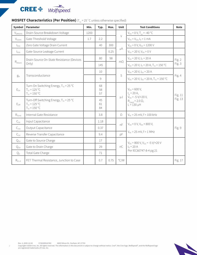
MOSFET Characteristics (Per Position) (TVJ = 25˚C unless otherwise specified)
Symbol Parameter Min. Typ. Max. Unit Test Conditions Note
V(BR)DSS Drain-Source Breakdown Voltage 1200V
VGS = 0 V, TVJ = -40 °C
VGS(th) Gate Threshold Voltage 1.7 2.2 VDS = VGS, ID = 1 mA
IDSS Zero Gate Voltage Drain Current 40 300µA
VGS = 0 V, VDS = 1200 V
IGSS Gate-Source Leakage Current 0.25 VGS = 20 V, VDS = 0 V
RDS(on)Drain-Source On-State Resistance (Devices Only)
80 98mΩ
VGS = 20 V, ID = 20 A Fig. 2Fig. 3145 VGS = 20 V, ID = 20 A, TVJ = 150 °C
gfs Transconductance10
SVDS = 20 V, IDS = 20 A
Fig. 49 VDS = 20 V, IDS = 20 A, TVJ = 150 °C
EOn
Turn-On Switching Energy, TVJ = 25 °CTVJ = 125 °CTVJ = 150 °C
685857
µJ
VDS = 600 V, ID = 20 A,VGS = -5 V/+20 V, RG(ext) = 2.0 Ω, L = 130 µH
Fig. 11Fig. 13
EOff
Turn-Off Switching Energy, TVJ = 25 °CTVJ = 125 °CTVJ = 150 °C
458184
RG(int) Internal Gate Resistance 3.8 Ω VAC = 25 mV, f = 100 kHz
Ciss Input Capacitance 1.18nF VGS = 0 V, VDS = 800 V,
VAC = 25 mV, f = 1 MHzFig. 9Coss Output Capacitance 0.37
Crss Reverse Transfer Capacitance 9.4 pF
QGS Gate to Source Charge 17
nCVDS = 800 V, VGS = -5 V/+20 VID = 20 APer IEC60747-8-4 pg 21
QGD Gate to Drain Charge 29
QG Total Gate Charge 71
Rth JC FET Thermal Resistance, Junction to Case 0.7 0.75 °C/W Fig. 17
Copyright ©2020 Cree, Inc. All rights reserved. The information in this document is subject to change without notice. Cree®, the Cree logo, Wolfspeed®, and the Wolfspeed logo are registered trademarks of Cree, Inc.
3Rev. 2, 2020-12-04 CCS020M12CM2 4600 Silicon Dr., Durham, NC 27703
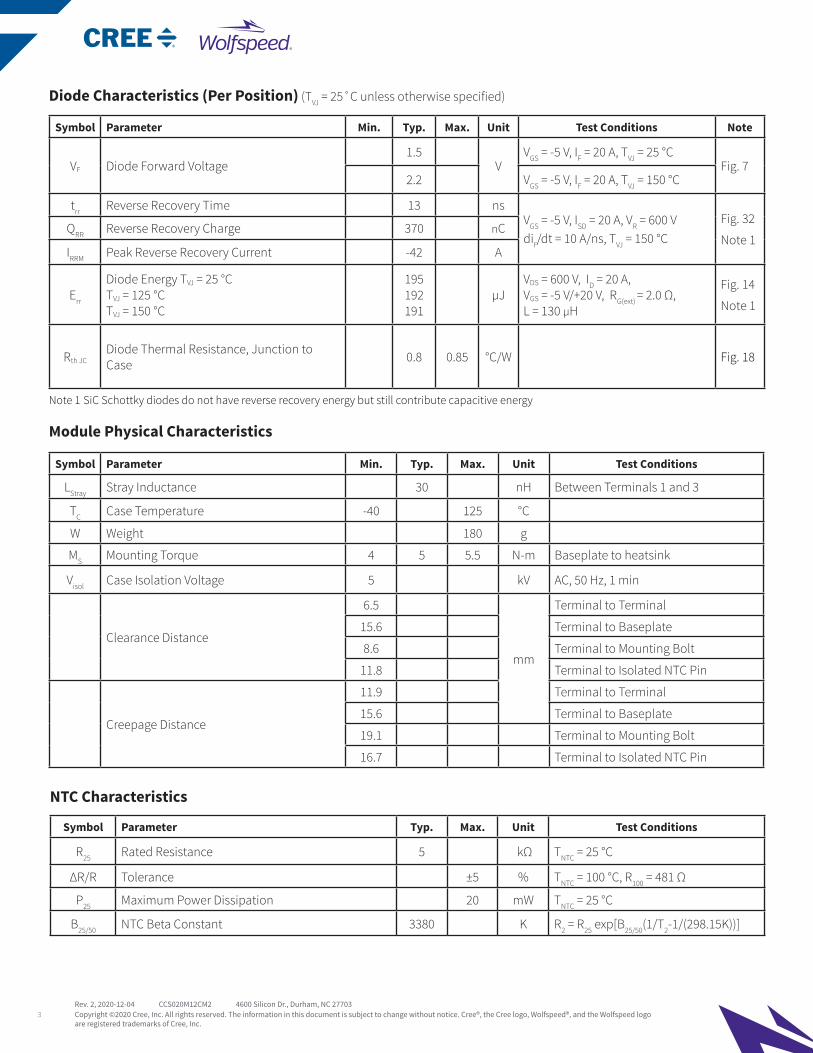
Module Physical Characteristics
Symbol Parameter Min. Typ. Max. Unit Test Conditions
LStray Stray Inductance 30 nH Between Terminals 1 and 3
TC Case Temperature -40 125 °C
W Weight 180 g
MS Mounting Torque 4 5 5.5 N-m Baseplate to heatsink
Visol Case Isolation Voltage 5 kV AC, 50 Hz, 1 min
Clearance Distance
6.5
mm
Terminal to Terminal
15.6 Terminal to Baseplate
8.6 Terminal to Mounting Bolt
11.8 Terminal to Isolated NTC Pin
Creepage Distance
11.9 Terminal to Terminal
15.6 Terminal to Baseplate
19.1 Terminal to Mounting Bolt
16.7 Terminal to Isolated NTC Pin
Diode Characteristics (Per Position) (TVJ = 25˚C unless otherwise specified)
Symbol Parameter Min. Typ. Max. Unit Test Conditions Note
VF Diode Forward Voltage1.5
VVGS = -5 V, IF = 20 A, TVJ = 25 °C
Fig. 72.2 VGS = -5 V, IF = 20 A, TVJ = 150 °C
trr Reverse Recovery Time 13 nsVGS = -5 V, ISD = 20 A, VR = 600 VdiF/dt = 10 A/ns, TVJ = 150 °C
Fig. 32
Note 1QRR Reverse Recovery Charge 370 nC
IRRM Peak Reverse Recovery Current -42 A
Err
Diode Energy TVJ = 25 °CTVJ = 125 °CTVJ = 150 °C
195192191
µJVDS = 600 V, ID = 20 A,VGS = -5 V/+20 V, RG(ext) = 2.0 Ω, L = 130 µH
Fig. 14
Note 1
Rth JCDiode Thermal Resistance, Junction to Case 0.8 0.85 °C/W Fig. 18
Note 1 SiC Schottky diodes do not have reverse recovery energy but still contribute capacitive energy
NTC Characteristics
Symbol Parameter Typ. Max. Unit Test Conditions
R25 Rated Resistance 5 kΩ TNTC = 25 °C
∆R/R Tolerance ±5 % TNTC = 100 °C, R100 = 481 Ω
P25 Maximum Power Dissipation 20 mW TNTC = 25 °C
B25/50 NTC Beta Constant 3380 K R2 = R25 exp[B25/50(1/T2-1/(298.15K))]
Copyright ©2020 Cree, Inc. All rights reserved. The information in this document is subject to change without notice. Cree®, the Cree logo, Wolfspeed®, and the Wolfspeed logo are registered trademarks of Cree, Inc.
4Rev. 2, 2020-12-04 CCS020M12CM2 4600 Silicon Dr., Durham, NC 27703
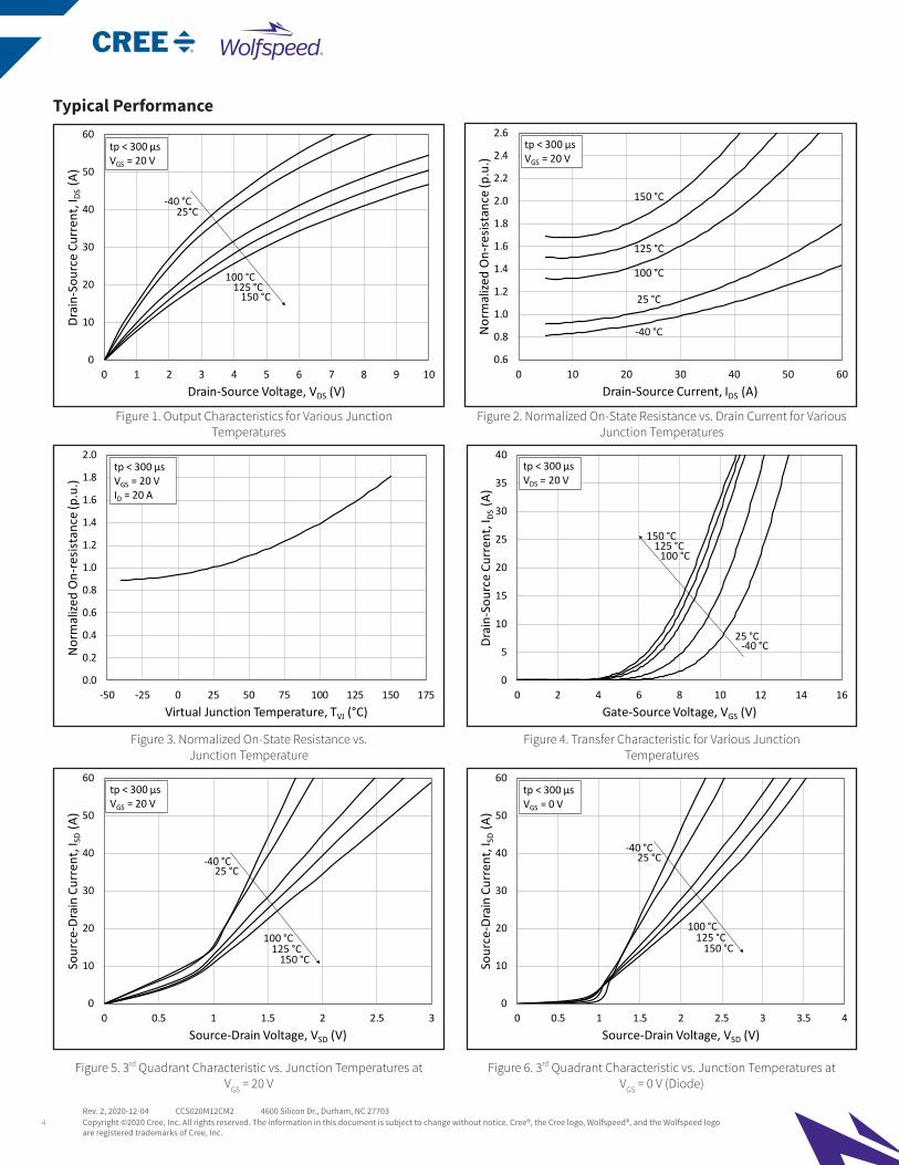
Figure 2. Normalized On-State Resistance vs. Drain Current for Various Junction Temperatures
Typical Performance
Figure 5. 3rd Quadrant Characteristic vs. Junction Temperatures at
VGS = 20 V
Figure 1. Output Characteristics for Various Junction Temperatures
Figure 3. Normalized On-State Resistance vs. Junction Temperature
Figure 4. Transfer Characteristic for Various JunctionTemperatures
Figure 6. 3rd Quadrant Characteristic vs. Junction Temperatures at
VGS = 0 V (Diode)
0
10
20
30
40
50
60
0 1 2 3 4 5 6 7 8 9 10
Dra
in-S
ourc
e Cu
rren
t, I D
S(A
)
Drain-Source Voltage, VDS (V)
150 °C125 °C
-40 °C
100 °C
tp < 300 μsVGS = 20 V
25°C
0.0
0.2
0.4
0.6
0.8
1.0
1.2
1.4
1.6
1.8
2.0
-50 -25 0 25 50 75 100 125 150 175
Nor
mal
ized
On-
resi
stan
ce (p
.u.)
Virtual Junction Temperature, TVJ (°C)
tp < 300 μsVGS = 20 VID = 20 A
0
5
10
15
20
25
30
35
40
0 2 4 6 8 10 12 14 16
Dra
in-S
ourc
e Cu
rren
t, I D
S(A
)
Gate-Source Voltage, VGS (V)
-40 °C25 °C
100 °C125 °C
150 °C
tp < 300 μsVDS = 20 V
0
10
20
30
40
50
60
0 0.5 1 1.5 2 2.5 3
Sour
ce-D
rain
Cur
rent
, ISD
(A)
Source-Drain Voltage, VSD (V)
150 °C125 °C
-40 °C
100 °C
tp < 300 μsVGS = 20 V
25 °C
0
10
20
30
40
50
60
0 0.5 1 1.5 2 2.5 3 3.5 4
Sour
ce-D
rain
Cur
rent
, ISD
(A)
Source-Drain Voltage, VSD (V)
-40 °C
100 °C
tp < 300 μsVGS = 0 V
25 °C
125 °C150 °C
0.6
0.8
1.0
1.2
1.4
1.6
1.8
2.0
2.2
2.4
2.6
0 10 20 30 40 50 60
Nor
mal
ized
On-
resi
stan
ce (p
.u.)
Drain-Source Current, IDS (A)
tp < 300 μsVGS = 20 V
25 °C
100 °C
125 °C
150 °C
-40 °C
Copyright ©2020 Cree, Inc. All rights reserved. The information in this document is subject to change without notice. Cree®, the Cree logo, Wolfspeed®, and the Wolfspeed logo are registered trademarks of Cree, Inc.
5Rev. 2, 2020-12-04 CCS020M12CM2 4600 Silicon Dr., Durham, NC 27703
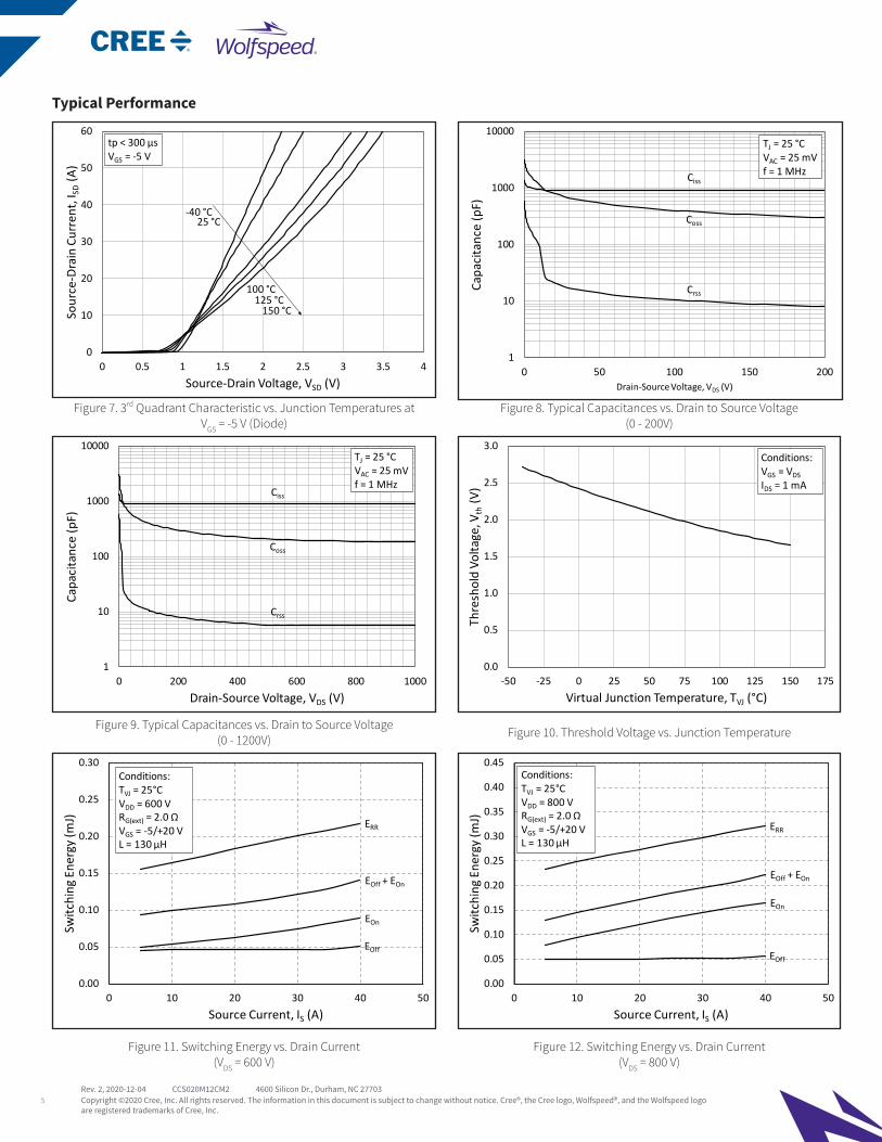
Figure 8. Typical Capacitances vs. Drain to Source Voltage(0 - 200V)
Typical Performance
Figure 11. Switching Energy vs. Drain Current(VDS = 600 V)
Figure 7. 3rd Quadrant Characteristic vs. Junction Temperatures at
VGS = -5 V (Diode)
Figure 9. Typical Capacitances vs. Drain to Source Voltage (0 - 1200V) Figure 10. Threshold Voltage vs. Junction Temperature
Figure 12. Switching Energy vs. Drain Current (VDS = 800 V)
0
10
20
30
40
50
60
0 0.5 1 1.5 2 2.5 3 3.5 4
Sour
ce-D
rain
Cur
rent
, ISD
(A)
Source-Drain Voltage, VSD (V)
-40 °C
100 °C
tp < 300 μsVGS = -5 V
25 °C
125 °C150 °C
EOff
EOn
EOff + EOn
ERR
0.00
0.05
0.10
0.15
0.20
0.25
0.30
0 10 20 30 40 50
Switc
hing
Ene
rgy
(mJ)
Source Current, IS (A)
Conditions:TVJ = 25°CVDD = 600 VRG(ext) = 2.0 ΩVGS = -5/+20 VL = 130 µH
EOff
EOn
EOff + EOn
ERR
0.00
0.05
0.10
0.15
0.20
0.25
0.30
0.35
0.40
0.45
0 10 20 30 40 50
Switc
hing
Ene
rgy
(mJ)
Source Current, IS (A)
Conditions:TVJ = 25°CVDD = 800 VRG(ext) = 2.0 ΩVGS = -5/+20 VL = 130 µH
0.0
0.5
1.0
1.5
2.0
2.5
3.0
-50 -25 0 25 50 75 100 125 150 175
Thre
shol
d Vo
ltage
, Vth
(V)
Virtual Junction Temperature, TVJ (°C)
Conditions:VGS = VDSIDS = 1 mA
1
10
100
1000
10000
0 200 400 600 800 1000
Capa
cita
nce
(pF)
Drain-Source Voltage, VDS (V)
Ciss
Coss
Crss
TJ = 25 °CVAC = 25 mVf = 1 MHz
1
10
100
1000
10000
0 50 100 150 200
Capa
cita
nce
(pF)
Drain-Source Voltage, VDS (V)
TJ = 25 °CVAC = 25 mVf = 1 MHzCiss
Coss
Crss
Copyright ©2020 Cree, Inc. All rights reserved. The information in this document is subject to change without notice. Cree®, the Cree logo, Wolfspeed®, and the Wolfspeed logo are registered trademarks of Cree, Inc.
6Rev. 2, 2020-12-04 CCS020M12CM2 4600 Silicon Dr., Durham, NC 27703
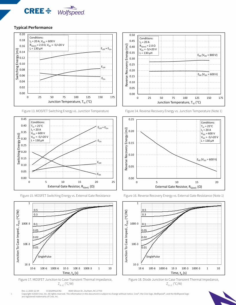
Figure 14. Reverse Recovery Energy vs. Junction Temperature (Note 1)
Typical Performance
Figure 17. MOSFET Junction to Case Transient Thermal Impedance, Zth JC (°C/W)
Figure 13. MOSFET Switching Energy vs. Junction Temperature
Figure 15. MOSFET Switching Energy vs. External Gate Resistance Figure 16. Reverse Recovery Energy vs. External Gate Resistance (Note 1)
Figure 18. Diode Junction to Case Transient Thermal Impedance, Zth JC (°C/W)
1E-3
10E-3
100E-3
1
1E-6 10E-6 100E-6 1E-3 10E-3 100E-3 1 10
Junc
tion
To C
ase
Impe
d., Z
thJC
(o C/W
)
Time, tp (s)
0.50.3
0.1
0.05
0.02
0.01
SinglePulse
1E-3
10E-3
100E-3
1
1E-6 10E-6 100E-6 1E-3 10E-3 100E-3 1 10
Junc
tion
To C
ase
Impe
d., Z
thJC
(o C/W
)
Time, tp (s)
0.50.3
0.1
0.05
0.02
0.01
SinglePulse
EOff
EOn
EOff + EOn
0.00
0.02
0.04
0.06
0.08
0.10
0.12
0.14
0.16
0.18
0.20
0 25 50 75 100 125 150 175
Switc
hing
Ene
rgy
(mJ)
Junction Temperature, TVJ (°C)
Conditions:IS = 20 A, VDD = 600 VRG(ext) = 2.0 Ω, VGS = -5/+20 VL = 130 µH
EOff
EOn
EOff + EOn
ERR
0.00
0.05
0.10
0.15
0.20
0.25
0.30
0.35
0.40
0.45
0 5 10 15 20 25
Switc
hing
Ene
rgy
(mJ)
External Gate Resistor, RG(ext) (Ω)
Conditions:TVJ = 25°CIS = 20 AVDD = 600 VVGS = -5/+20 VL = 130 µH
ERR (VDD = 600 V)
ERR (VDD = 800 V)
0.00
0.05
0.10
0.15
0.20
0.25
0.30
0.35
0.40
0.45
0.50
0 25 50 75 100 125 150 175
Reve
rse
Reco
very
Ene
rgy
(mJ)
Junction Temperature, TVJ (°C)
Conditions:IS = 20 ARG(ext) = 2.0 ΩVGS = -5/+20 VL = 130 µH
ERR (VDD = 600 V)
0.00
0.05
0.10
0.15
0.20
0.25
0 5 10 15 20
Reve
rse
Reco
very
Ene
rgy
(mJ)
External Gate Resistor, RG(ext) (Ω)
Conditions:TVJ = 25°CIS = 20 AVDD = 600 VVGS = -5/+20 VL = 130 µH
Copyright ©2020 Cree, Inc. All rights reserved. The information in this document is subject to change without notice. Cree®, the Cree logo, Wolfspeed®, and the Wolfspeed logo are registered trademarks of Cree, Inc.
7Rev. 2, 2020-12-04 CCS020M12CM2 4600 Silicon Dr., Durham, NC 27703
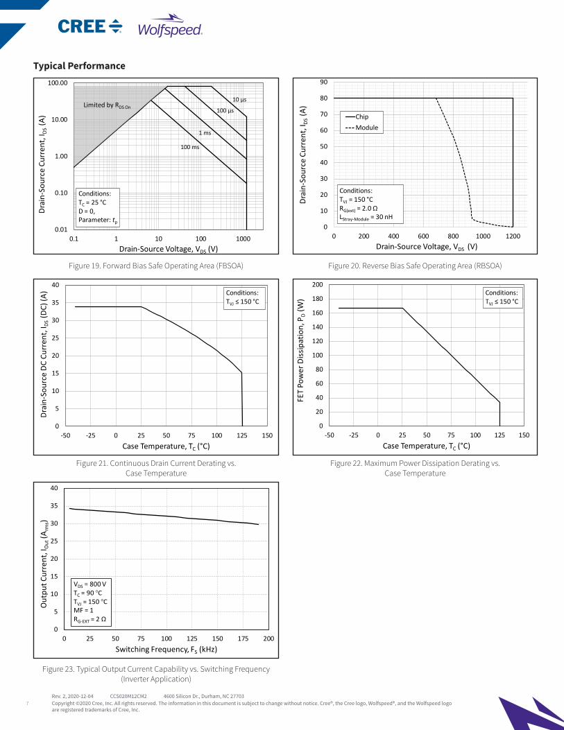
Figure 20. Reverse Bias Safe Operating Area (RBSOA)
Typical Performance
Figure 19. Forward Bias Safe Operating Area (FBSOA)
Figure 21. Continuous Drain Current Derating vs. Case Temperature
Figure 22. Maximum Power Dissipation Derating vs. Case Temperature
0
5
10
15
20
25
30
35
40
-50 -25 0 25 50 75 100 125 150
Dra
in-S
ourc
e D
C Cu
rren
t, I D
S(D
C) (A
)
Case Temperature, TC (°C)
Conditions:TVJ ≤ 150 °C
0
10
20
30
40
50
60
70
80
90
0 200 400 600 800 1000 1200
Drai
n-So
urce
Cur
rent
, IDS
(A)
Drain-Source Voltage, VDS (V)
ChipModule
Conditions:TVJ = 150 °C RG(ext) = 2.0 ΩLStray-Module = 30 nH
0
20
40
60
80
100
120
140
160
180
200
-50 -25 0 25 50 75 100 125 150
FET
Pow
er D
issi
patio
n, P
D(W
)
Case Temperature, TC (°C)
Conditions:TVJ ≤ 150 °C
0.01
0.10
1.00
10.00
100.00
0.1 1 10 100 1000
Dra
in-S
ourc
e Cu
rren
t, I D
S(A
)
Drain-Source Voltage, VDS (V)
100 µs
1 ms
10 µs
Conditions:TC = 25 °CD = 0, Parameter: tp
100 ms
Limited by RDS On
0
5
10
15
20
25
30
35
40
0 25 50 75 100 125 150 175 200
Out
put C
urre
nt, I
Out
(Arm
s)
Switching Frequency, FS (kHz)
VDS = 800 VTC = 90 °CTVJ = 150 °CMF = 1RG-EXT = 2 Ω
Figure 23. Typical Output Current Capability vs. Switching Frequency (Inverter Application)
Copyright ©2020 Cree, Inc. All rights reserved. The information in this document is subject to change without notice. Cree®, the Cree logo, Wolfspeed®, and the Wolfspeed logo are registered trademarks of Cree, Inc.
8Rev. 2, 2020-12-04 CCS020M12CM2 4600 Silicon Dr., Durham, NC 27703
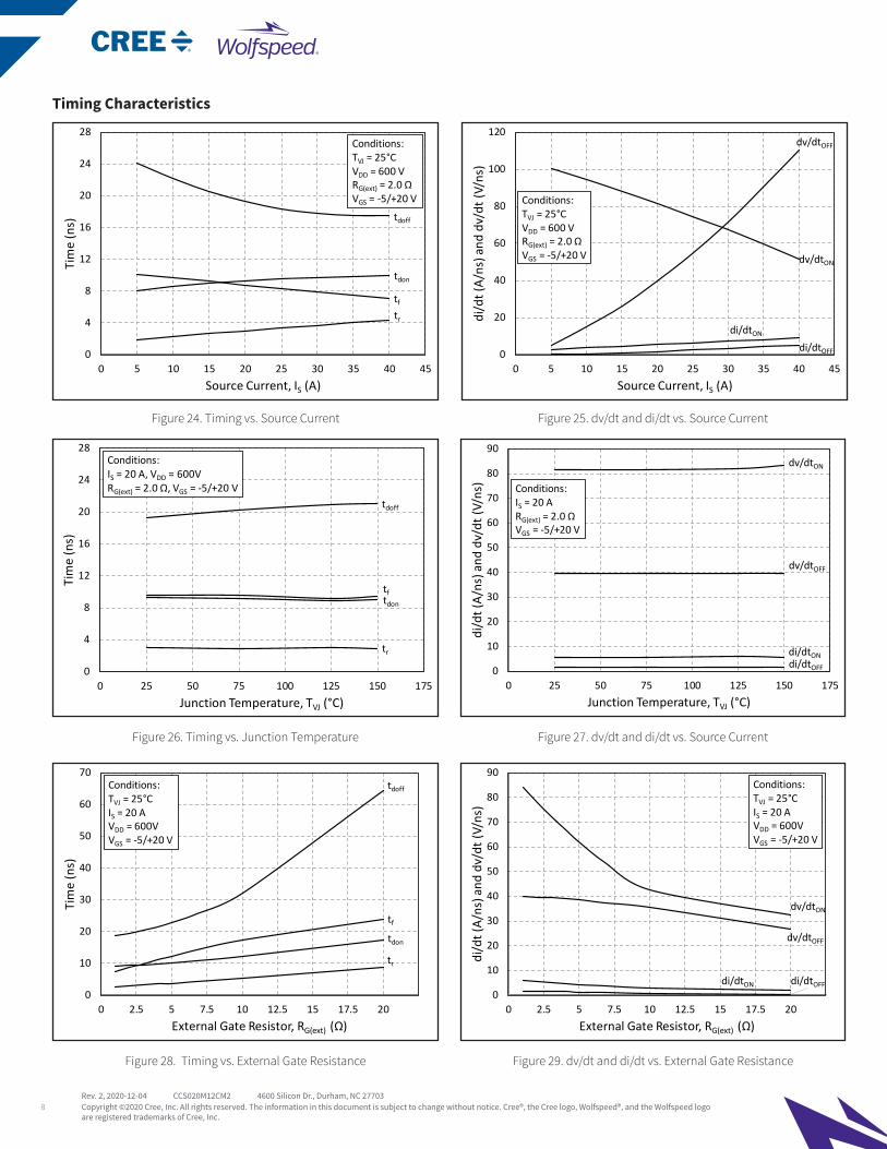
Figure 25. dv/dt and di/dt vs. Source Current
Timing Characteristics
Figure 24. Timing vs. Source Current
Figure 26. Timing vs. Junction Temperature Figure 27. dv/dt and di/dt vs. Source Current
tdoff
tftdon
tr
0
4
8
12
16
20
24
28
0 25 50 75 100 125 150 175
Tim
e (n
s)
Junction Temperature, TVJ (°C)
Conditions:IS = 20 A, VDD = 600VRG(ext) = 2.0 Ω, VGS = -5/+20 V
dv/dtOFF
dv/dtON
di/dtOFF
di/dtON
0
10
20
30
40
50
60
70
80
90
0 25 50 75 100 125 150 175
di/d
t (A/
ns) a
nd d
v/dt
(V/n
s)
Junction Temperature, TVJ (°C)
Conditions:IS = 20 ARG(ext) = 2.0 ΩVGS = -5/+20 V
tdoff
tf
tdon
tr
0
4
8
12
16
20
24
28
0 5 10 15 20 25 30 35 40 45
Tim
e (n
s)
Source Current, IS (A)
Conditions:TVJ = 25°CVDD = 600 VRG(ext) = 2.0 ΩVGS = -5/+20 V
Figure 28. Timing vs. External Gate Resistance Figure 29. dv/dt and di/dt vs. External Gate Resistance
tdoff
tf
tdon
tr
0
10
20
30
40
50
60
70
0 2.5 5 7.5 10 12.5 15 17.5 20
Tim
e (n
s)
External Gate Resistor, RG(ext) (Ω)
Conditions:TVJ = 25°CIS = 20 AVDD = 600VVGS = -5/+20 V
dv/dtOFF
dv/dtON
di/dtOFFdi/dtON0
10
20
30
40
50
60
70
80
90
0 2.5 5 7.5 10 12.5 15 17.5 20
di/d
t (A/
ns) a
nd d
v/dt
(V/n
s)
External Gate Resistor, RG(ext) (Ω)
Conditions:TVJ = 25°CIS = 20 AVDD = 600VVGS = -5/+20 V
dv/dtOFF
dv/dtON
di/dtOFF
di/dtON
0
20
40
60
80
100
120
0 5 10 15 20 25 30 35 40 45
di/d
t (A/
ns) a
nd d
v/dt
(V/n
s)
Source Current, IS (A)
Conditions:TVJ = 25°CVDD = 600 VRG(ext) = 2.0 ΩVGS = -5/+20 V
Copyright ©2020 Cree, Inc. All rights reserved. The information in this document is subject to change without notice. Cree®, the Cree logo, Wolfspeed®, and the Wolfspeed logo are registered trademarks of Cree, Inc.
9Rev. 2, 2020-12-04 CCS020M12CM2 4600 Silicon Dr., Durham, NC 27703
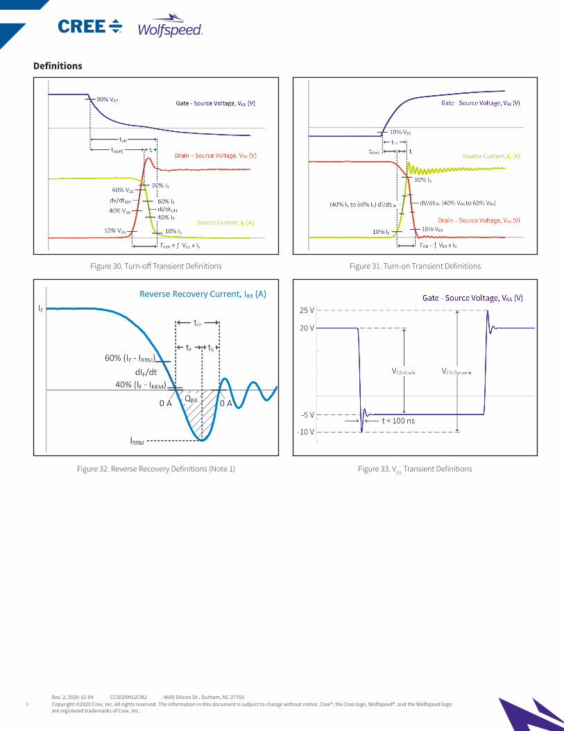
Figure 31. Turn-on Transient Definitions
Definitions
Figure 30. Turn-off Transient Definitions
Figure 32. Reverse Recovery Definitions (Note 1) Figure 33. VGS Transient Definitions
Copyright ©2020 Cree, Inc. All rights reserved. The information in this document is subject to change without notice. Cree®, the Cree logo, Wolfspeed®, and the Wolfspeed logo are registered trademarks of Cree, Inc.
10Rev. 2, 2020-12-04 CCS020M12CM2 4600 Silicon Dr., Durham, NC 27703
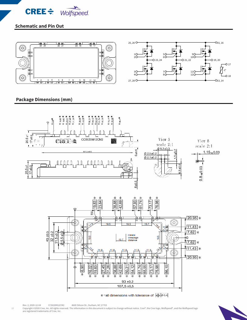
Schematic and Pin Out
Package Dimensions (mm)
CAS120M12BM2HA1940-A019
5
5
4
4
3
3
2
2
1
1
D D
C C
B B
A A
V+
Mid
G1K1
G2K2
G5K5
Mid
NTC1
G6K6 NTC2
G3K3
Mid
G4K4
V-
V+
V-
25, 26 15, 16
1 5 92 6 10
23, 24 21, 22 19, 20
17
3 7 114 8 12 18
13, 1427, 28
-t°
-t°

Copyright ©2020 Cree, Inc. All rights reserved. The information in this document is subject to change without notice. Cree®, the Cree logo, Wolfspeed®, and the Wolfspeed logo are registered trademarks of Cree, Inc.
11Rev. 2, 2020-12-04 CCS020M12CM2 4600 Silicon Dr., Durham, NC 27703
Recommendations for PCB Mounting Stand-offs
In order to mount the PCB onto the module, it is recommended to use four PCB mounting stand-offs by usingself-tapping screws. Following is the recommended self-tapping screw with its torque requirements:
> Ejot DELTA PT WN 5451 K25x8 : Mmax = 0.4Nm ± 10%
Installation of self-tapping screws can be done both by hand or by using an electric screw driver. For an electricscrew driver the recommended maximum speed is 300 RPM.
(Note: Do not use pneumatic screw driver to install self-tapping screws).
The recommended effective length of screw threads entering the PCB mounting stand-offs should be in between4mm to 6.5mm range.
(Note: Self-tapping screws must be inserted straight into the PCB mounting stand-offs)
PCB Mounting Stand-offs (Marked Red)
Copyright ©2020 Cree, Inc. All rights reserved. The information in this document is subject to change without notice. Cree®, the Cree logo, Wolfspeed®, and the Wolfspeed logo are registered trademarks of Cree, Inc.
12Rev. 2, 2020-12-04 CCS020M12CM2 4600 Silicon Dr., Durham, NC 27703
Notes
• This product has not been designed or tested for use in, and is not intended for use in, applications implanted into the human body nor in applications in which failure of the product could lead to death, personal injury or property damage, including but not limited to equipment used in the operation of nuclear facilities, life-support machines, cardiac defibrillators or similar emergency medical equipment, aircraft navigation or communication or control systems, or air traffic control systems.
• The SiC MOSFET module switches at speeds beyond what is customarily associated with IGBT-based modules. Therefore, special precautions are required to realize optimal performance. The interconnection between the gate driver and module housing needs to be as short as possible. This will afford optimal switching time and avoid the potential for device oscillation. Also, great care is required to insure minimum inductance between the module and DC link capacitors to avoid excessive VDS overshoot.


![ECEN325: Electronics Spring 2021[Sedra/Smith] L x V GC x V GS V x V GS V DS • When V DS V GS-V TH=V OV, V GC no longer exceeds V TH, resulting in the channel “pinching off” and](https://img.pdfslide.us/doc/110x75/612a01ce79234c2dda6a1604/ecen325-electronics-spring-2021-sedrasmith-l-x-v-gc-x-v-gs-v-x-v-gs-v-ds-a.jpg)