Embed Size (px)
Citation preview

(12) United States Patent Machado et al.
US007.9594.73B2
US 7.959,473 B2 Jun. 14, 2011
(10) Patent No.: (45) Date of Patent:
(54) UNIVERSAL CONNECTOR ASSEMBLY AND METHOD OF MANUFACTURING
(75) Inventors: Russell Lee Machado, San Diego, CA (US); Victor H. Renteria, Poway, CA (US); Thuyen Dinh, San Diego, CA (US)
(73) Assignee: Pulse Engineering, Inc., San Diego, CA (US)
(*) Notice: Subject to any disclaimer, the term of this patent is extended or adjusted under 35 U.S.C. 154(b) by 0 days.
(21) Appl. No.: 12/871,801
(22) Filed: Aug. 30, 2010
(65) Prior Publication Data
US 2011 FOO59647 A1 Mar. 10, 2011
Related U.S. Application Data (63) Continuation of application No. 12/705.949, filed on
Feb. 15, 2010, now Pat. No. 7,786,009, which is a continuation of application No. 12/151,343, filed on May 5, 2008, now Pat. No. 7,661,994, which is a continuation of application No. 1 1/827,074, filed on Jul. 9, 2007, now Pat. No. 7,367,851, which is a continuation of application No. 1 1/170,583, filed on Jun. 28, 2005, now Pat. No. 7,241,181.
(60) Provisional application No. 60/583,989, filed on Jun. 29, 2004.
(51) Int. Cl. HOIR 24/00 (2006.01)
(52) U.S. Cl. .............. 439/676; 439/620.06; 439/620.15; 439/541.5
(58) Field of Classification Search .................. 439/676, 439/620.06, 620.07, 620.15, 620.16, 620.17,
439/620.18, 620.23, 541.5 See application file for complete search history.
(56) References Cited
U.S. PATENT DOCUMENTS
3.422,394 A 1/1969 Antes 4,109,986 A 8, 1978 Mouissie 4,461.522 A 7, 1984 Bakermans et al. 4,695,115 A 9, 1987 Talend
(Continued)
FOREIGN PATENT DOCUMENTS
EP 1011176 6, 2000
(Continued)
OTHER PUBLICATIONS
Integrated Connector Modules 10/100Base-TX belMag with LEDS data sheet, 2000 Bel Fuse Inc., 2 pages.
(Continued)
Primary Examiner — Tho DTa (74) Attorney, Agent, or Firm — GaZdzinski & Associates, PC
(57) ABSTRACT
An advanced modular plug connector assembly incorporat ing an insert assembly disposed in the rear portion of the connector housing. In one embodiment, the connector has a plurality of ports in multi-row configuration, and the insert assembly includes a Substrate adapted to receive one or more electronic components such as choke coils, transformers, or other signal conditioning elements or magnetics. The Sub strate also interfaces with the conductors of two modular ports of the connector, and is removable from the housing such that an insert assembly of a different electronics or terminal configuration can be substituted therefor. In this fashion, the connector can be configured to a plurality of different standards (e.g., Gigabit Ethernet and 10/100). In yet another embodiment, the connector assembly comprises a plurality of light sources (e.g., LEDs) received within the housing. Methods for manufacturing the aforementioned embodiments are also disclosed.
43 Claims, 27 Drawing Sheets

US 7,959.473 B2 Page 2
U.S. PATENT DOCUMENTS 6,176,741 B1 1/2001 Shutter 6,193,560 B1 2/2001 Morana et al.
4,701,002 10, 1987 Mouissie 6,196,879 B1 3/2001 Hess et al. 4,726,638 2f1988 Farrar et al. 6,224,425 B1 5/2001 Shutter 4,772,224 9, 1988 Talend 6,325,664 B1 12/2001 Someda et al. 4,978,317 12/1990 Pocrass 6,352,446 B2 3/2002 Ezawa et al. 4,995,834 2, 1991 Hasegawa 6,361,357 B1 3/2002 Stillwell et al. 5,011,438 4/1991 Awbrey 6,368,159 B1 4/2002 Hess et al. 5,015,204 5, 1991 Sakamoto et al. 6,409,548 B1 6/2002 Guttierez 386. 38. St. 1 6.425,781 B1 7/2002 Bernstein et al. 5.39442 8, 1992 S IE I. 6,428,361 B1 8/2002 Imschweiler et al.
k --- 6,471,551 B2 10/2002 Morana et al. 5,178,563 1/1993 Reed 6,478,611 B1 1 1/2002 Hyland 5,239,748 8, 1993 Hamilton 6,483,712 B1 1 1/2002 Oliphant et al. 5,282,759 2, 1994 Sakamoto et al. 6,537,110 B1 3/2003 Korsunsky et al. 5,362.257 11/1994 Neal et al. 6,554,638 B1 4/2003 Hess et al. Si; 38: Real 6,568,966 B1* 5/2003 Korsunsky et al. ........... 439/676 5.403.207 4, 1995 yet al. 6,585,540 B2 7/2003 Gutierrez et al.
W - 6,593,840 B2 7/2003 Morrison et al. 5,456,619 10/1995 Belopolsky et al. 6,642,827 B1 1 1/2003 McWilliams et al. 5,475,921 12/1995 Johnston 6,702,610 B2 * 3/2004 Zheng et al. ............... 439/541.5 5,478,261 12/1995 Bogese, II 6,761,595 B1 7/2004 Zheng etal 5,496,195 3, 1996 Reed wr. 6,769,936 B2 8, 2004 Gutierrez et al.
7, 1996 Goodall et al. 6,773,298 B2 8/2004 Gutierrez et al. 5,531,612 5,562,507 10, 1996 Kan 6,773,302 B2 8/2004 Gutierrez et al. s: leg y 6,786,772 B1* 9/2004 Liu .......................... 439/620.06 5,639,267 6, 1997 Loudermilk ... E: 58. SE, d 5.647.767 7, 1997 Scheer et al. sy sy achado et al. w I 6,962,511 B2 11/2005 Gutierrez et al.
5,687,233 EE Silk et al. 6,964,587 B2 11/2005 Colantuono et al. 9. '92. Bush,detal 7,048,590 B2 5/2006 Colantuono et al.
- w 7,052,315 B2 * 5/2006 Murr et al. ................. 439/540.1 5,741, 152 4, 1998 Boutros 7,086,909 B2 8/2006 Colantuono et al. 5,759,067 6, 1998 Scheer 7.241,181 B2 7/2007 Machado et al. 5,766,043 6, 1998 Talend 7,717,749 B2 5/2010 Chen et al. 33. 23. E. 2001/0027055 A1 10/2001 Laity et al. 5,876339 3, 1999 Morin et all 2002/000991.0 A1 1/2002 Posey et al. 5.885.100 3/1999 Talenderal 2002/0058432 A1 5, 2002 Chen et al. 5924,890 7, 1999 Morinet al. 2002fOO81901 A1 6, 2002 Ma et al. 5928,005 7, 1999 Li etal 2002/0146940 A1 10, 2002 Colantuono et al. 5934,940 8, 1999 Maranto etal 2003/0022553. A 1 1/2003 Chen et al. 5-97805 10, 1999 Belopolsky et al 2003/0207622 A1 11/2003 Gutierrez et al.
3. 3. . 1992 St. al FOREIGN PATENT DOCUMENTS -- sys- ea.
6,005,463 12/1999 Lint et al. JP 11-273.795 10, 1999 6,019,631 2/2000 Chen JP 2000-182724 6, 2000 6,062,908 5, 2000 Jones WO WOOO,22697 4/2000 6,080,011 6, 2000 Tsao et al. 6,116,963 9, 2000 Shutter OTHER PUBLICATIONS
&E 1939 yang Product Catalogue of Kingbright Electronic Co., Ltd., published 6,139,366 10, 2000 van Woensel 2000-2001, 5 pages. 6,159,050 12/2000 Belopolsky et al. Integrated Connector Modules I 0/100Base-TX belMag with LEDS 6,162,089 12/2000 Costello et al. data sheet, 2000 Bel Fuse Inc., 2 pages. 6,171,152 B1 1/2001 Kunz 6,174,194 B1 1/2001 Bleicher et al. * cited by examiner

U.S. Patent Jun. 14, 2011 Sheet 1 of 27 US 7.959,473 B2
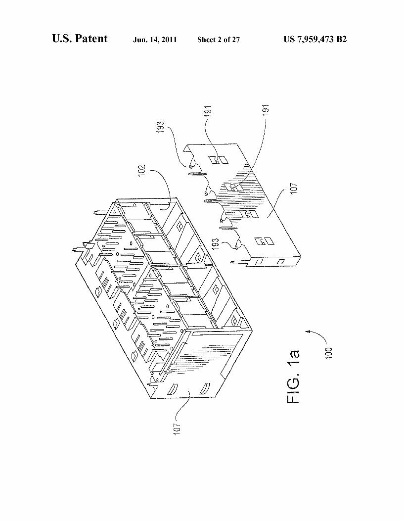
U.S. Patent Jun. 14, 2011 Sheet 2 of 27 US 7.959,473 B2
e e
-. CO r

U.S. Patent Jun. 14, 2011 Sheet 3 of 27 US 7.959,473 B2
U.S. Patent Jun. 14, 2011 Sheet 4 of 27 US 7.959,473 B2
N rue rarer

U.S. Patent Jun. 14, 2011 Sheet 5 Of 27 US 7.959,473 B2

US 7.959,473 B2 Sheet 6 of 27 Jun. 14, 2011 U.S. Patent

U.S. Patent Jun. 14, 2011 Sheet 7 Of 27 US 7.959,473 B2
U.S. Patent Jun. 14, 2011 Sheet 8 of 27 US 7.959,473 B2

U.S. Patent Jun. 14, 2011 Sheet 9 Of 27 US 7.959,473 B2
U.S. Patent Jun. 14, 2011 Sheet 10 of 27 US 7.959,473 B2

U.S. Patent Jun. 14, 2011 Sheet 11 of 27 US 7.959,473 B2
FIG. 1j

U.S. Patent Jun. 14, 2011 Sheet 12 of 27
152
us 7,959.473 B2 U.S. Patent

US 7.959,473 B2 Jun. 14, 2011 Sheet 14 of 27 U.S. Patent
7TTT
| NVV | fea SNS
U.S. Patent Jun. 14, 2011 Sheet 15 of 27 US 7.959,473 B2
s -issue.
5
U.S. Patent Jun. 14, 2011 Sheet 16 of 27 US 7.959,473 B2
5
U.S. Patent Jun. 14, 2011 Sheet 17 Of 27 US 7.959,473 B2

U.S. Patent Jun. 14, 2011 Sheet 18 of 27 US 7.959,473 B2

U.S. Patent Jun. 14, 2011 Sheet 19 Of 27 US 7.959,473 B2
N E. Z 7.
&
s
re
s
3.
U.S. Patent Jun. 14, 2011 Sheet 20 Of 27 US 7.959,473 B2
S

U.S. Patent Jun. 14, 2011 Sheet 21 of 27 US 7.959,473 B2
U.S. Patent Jun. 14, 2011 Sheet 22 of 27 US 7.959,473 B2

U.S. Patent Jun. 14, 2011 Sheet 23 Of 27 US 7.959,473 B2

US 7.959,473 B2 Sheet 24 of 27 Jun. 14, 2011 U.S. Patent

U.S. Patent Jun. 14, 2011 Sheet 25 of 27 US 7.959,473 B2
START
502
FORM HOUSING
500 504 PROVIDE CONDUCTOR -
N SES 506
DEFORM CONDUCTORS
508 MOLDINSERT SUBASSEMBLY
51O
MATE SUBASSEMBLY'S
512 PROVIDE UPPER AND LOWERTERMINALS
514
MOLD BODYELEMENTS
(N-
(a) F.G. 5
(PART 1 OF 3)

U.S. Patent Jun. 14, 2011 Sheet 26 of 27 US 7.959,473 B2
(a) (NJ
516
FORMUPPER SUBSTRATE
500 518
N FORMLOWER SUBSTRATE 520
PROVIDE ELECTRONICS (IF ANY)
522 MATEELECTRONICS - TOUPPER SUBSTRATE
524 PLACE REMAINING
ELECTRONICS IN BODY 526
MATE BODY COMPONENTS
528 ENCAPSULATE IF
DESIRED -
(NJ
F.G. 5 (PART 2 OF 3)

U.S. Patent Jun. 14, 2011 Sheet 27 Of 27 US 7.959,473 B2
(N-
530 MATE UPPER SUBSTRATE
500 -- 532 MATE INSERTASSEMBLY'S O
-- 534 INSERT TERMINAL ---
- ASSEES 536
NSERTLowR SUBSTRATE WITH ASSEMBLY'S
538
ADD NOSE SHIELD
(N-u
F.G. 5 (PART 3 OF 3)

US 7,959,473 B2 1.
UNIVERSAL CONNECTOR ASSEMBLY AND METHOD OF MANUFACTURING
PRIORITY
This application is a continuation of co-owned and U.S. patent application Ser. No. 12/705,949 filed Feb. 15, 2010 of the same title, which is a continuation of co-owned U.S. patent application Ser. No. 12/151,343 filed May 5, 2008 of the same title, now issued as U.S. Pat. No. 7,661,994, which is a continuation of co-owned U.S. patent application Ser. No. 1 1/827,074 filed Jul. 9, 2007 of the same title, now issued as U.S. Pat. No. 7,367,851, which is a continuation of co-owned U.S. patent application Ser. No. 11/170,583 filed Jun. 28, 2005 of the same title, now issued as U.S. Pat. No. 7,241,181, which claims priority to U.S. Provisional Patent Application Ser. No. 60/583,989 filed Jun. 29, 2004 of the same title, each of the foregoing being incorporated herein by reference in its entirety.
COPYRIGHT
A portion of the disclosure of this patent document con tains material that is subject to copyright protection. The copyright owner has no objection to the facsimile reproduc tion by anyone of the patent document or the patent disclo sure, as it appears in the Patent and Trademark Office patent files or records, but otherwise reserves all copyright rights whatsoever.
FIELD OF THE INVENTION
The present invention relates generally to electronic com ponents, and particularly to an improved design for, and method of manufacturing a single- or multi-connector assem bly which may include internal electronic components.
DESCRIPTION OF RELATED TECHNOLOGY
Modular connectors, such as for example those of the “RJ' configuration, are well known in the electronics industry. Such connectors are adapted to receive one or more modular plugs of varying type (e.g., RJ-45 or RJ-11), and communi cate signals between the terminals of the modular plug and the parent device with which the connector is associated. Com monly, some form of signal conditioning (e.g., filtering, Volt age transformation, or the like) is performed by the connector on the signals passing through it. Many different considerations are involved with producing
an effective and economically viable connector design. Such considerations include, for example: (i) Volume and “foot print’ available for the connector; (ii) the need for electrical status indicators (e.g., LEDs); (iii) the cost and complexity associated with assembling and manufacturing the device; (iv) the ability to accommodate various electrical components and signal conditioning configurations, (v) the electrical and noise performance of the device; (vi) the reliability of the device; (vii) the ability to modify the design to accommodate complementary technologies; (viii) compatibility with exist ing terminal and "pin out standards and applications; (ix) ability to configure the connectoras one of a plurality of ports, potentially having individually variant internal component configurations, and (ix) potentially the maintenance or replacement of defective components.
Electrical connectors (including modular jacks) are increasingly used in data networking applications, such as wired or wireless LANs, whether for computers or other
15
25
30
35
40
45
50
55
60
65
2 electronic devices (such as routers, gateways, hubs, Switching centers, digital set-top boxes, etc.). Increasing requirements for data connectivity and capability are driving greater adop tion of these connectors across a broader spectrum of appli cations. Increased data rate requirements, such as those man dated under so-called "gigabit Ethernet’ (GBE) standards, are also increasing the performance demands on these con nectors. As more capability and components (such as both discrete and integrated circuitry) are disposed within the con nector, more efficient use of the available volume within the connector, and more efficient heat dissipation, are also required. The foregoing factors have resulted in myriad different
(and often highly specialized) configurations for modular connectors in the prior art. Many of these designs utilize an internal PCB or substrate for carrying electronic or signal conditioning components internal to the connector housing. For example, U.S. Pat. No. 5,069,641 to Sakamoto, et al. issued Dec. 3, 1991 and entitled “Modular jack” discloses a modular jack to be mounted on a circuit board, and the modu lar jack has a printed board containing a noise Suppressing electronic element in a housing. The printed board is fitted with contactors for contacting with plugs and terminals to be used for mounting the modular jack on the circuit board. The contactors and the terminals are electrically connected with the noise Suppressing electronic element by wires on the printed board.
U.S. Pat. No. 5,531,612 to Goodall, et al. issued Jul. 2, 1996 entitled “Multi-port modularjackassembly' discloses a modular jack assembly for mounting to a printed circuit board, is shown comprising a plurality of modular jacks assembled to a common integral housing and disposed in back-to-back mirror image symmetry. Shielding, is provided around the connector assembly and shielding between the two rows is also provided for Suppressing cross-talk there between. The design is compact, providing for a large number of ports without increasing the length of the connector assem bly, whilst also providing good access to the resilient locking latches of complementary modular plugs received by the jacks.
U.S. Pat. No. 5,587,884 to Raman issued Dec. 24, 1996 and entitled “Electrical connector jack with encapsulated signal conditioning components' discloses a modular jack electrical connector assembly Suitable for conditioning the signals in unshielded twisted pair wires for use with network compo nents is disclosed. The modular jack comprises a conven tional insulative housing and an insert Subassembly including insert molded front insert member and rear insert member. Contact terminals for mating with a modular plug extend from the front insert member and into the rear insert member. The rear insert member also includes signal conditioning components such as common mode choke coils, filter circuits and transformers Suitable for conditioning the twisted pair signals for used in applications such as for input to and output from IEEE 10 Base-T network components.
U.S. Pat. No. 5,647,767 to Scheer, et al. issued Jul.15, 1997 and entitled “Electrical connector jack assembly for signal transmission' discloses a modular jack electrical connector assembly for conditioning the signals in unshielded twisted pair wires for use with network components. The modular jack comprises a conventional insulative housing and an insert Subassembly including an insert molded front insert member and a rear insert member. Contact terminals for mating with a modular plug extend from the front insert member and into the rear insert member. The rear insert member also includes signal conditioning components such as common mode choke coils, filter circuits and transformers
US 7,959,473 B2 3
Suitable for conditioning the twisted pair signals for used in applications such as for input to and output from IEEE 10 Base-T network components. The rear insert member includes an insert molded body which stabilizes the position of the contact terminals and leads extending from the rear insert member for attachment to external circuits, such as the external printed circuit board containing the interface proces sor for the specific application.
U.S. Pat. No. 5,759,067 entitled “Shielded Connector' to Scheer exemplifies a common prior art approach. In this configuration, one or more PCBs are disposed within the connector housing in a vertical planar orientation such that an inner face of the PCB is directed toward an interior of the assembly and an outerface directed toward an exterior of the assembly.
U.S. Pat. No. 6,171,152 to Kunz issued Jan. 9, 2001 entitled “Standard footprint and form factor RJ-45 connector with integrated signal conditioning for high speed networks’ discloses an RJ-45 style modular connector having a plastic rectangular housing with an open front end to receive a matching RJ-45 style modular jack, and an opposite open back end. A contact spring assembly of a plurality of wires in separate circuits passes forward through said open back end into the back of said open front end of the housing. The contact assembly also includes a plastic block that Supports the plurality of wires by a right angle turn and is vertically oriented with respect to the plurality of wires, and the plastic block inserts and locks into the open back end of the housing. A set of mounting pins is disposed at a bottom edge of the plastic block for connection to a printed motherboard. A signal conditioning part is disposed in the plastic block for providing signal conditioning of signals passing from said set of mounting pins to the contact spring assembly.
U.S. Pat. No. 6,585,540 to Gutierrez, et al. issued Jul. 1, 2003 and entitled “Shielded microelectronic connector assembly and method of manufacturing discloses a multi connector electronic assembly incorporating different noise shield elements which reduce noise interference and increase performance. In one embodiment, the connector assembly comprises a plurality of connectors with associated electronic components arranged in two parallel rows, one disposed atop the other. The assembly utilizes a substrate shield which mitigates noise transmission through the bottom Surface of the assembly, as well as an external 'wrap-around shield to mitigate noise transmission through the remaining external Surfaces. In a second embodiment, the connector assembly further includes a top-to-bottom shield interposed between the top and bottom rows of connectors to reduce noise trans mission between the rows of connectors, and a plurality of front-to-back shield elements disposed between the elec tronic components of respective top and bottom row connec tors to limit transmission between the electronic components.
U.S. Pat. No. 6,769,936 to Gutierrez, et al. issued Aug. 3, 2004 entitled “Connector with insert assembly and method of manufacturing discloses a modular plug connector assembly incorporating a Substantially planar, low profile removable insert assembly with associated Substrate disposed in the rear portion of the connector housing, the Substrate adapted to optionally receive one or more electronic components. In one embodiment, the connector assembly comprises a single port with a single insert assembly. The conductors and terminals of the connector are retained within respective molded carri ers which are received within the insert assembly. A plurality of light sources (e.g., LEDs) are also received within the housing, the conductors of the LEDs mated with conductive
10
15
25
30
35
40
45
50
55
60
65
4 traces on the substrate of the insert assembly. In another embodiment, the connector assembly comprises a multi-port “1XN” device.
U.S. Pat. No. 6,773.302 to Gutierrez, et al. issued Aug. 10, 2004 entitled "Advanced microelectronic connector assem bly and method of manufacturing discloses a modular plug connector assembly incorporating a substrate disposed in the rear portion of the connector housing, the Substrate adapted to receive one or more electronic components such as choke coils, transformers, or other signal conditioning elements or magnetics. In one embodiment, the connector assembly com prises a single port pair with a single Substrate disposed in the rear portion of the housing. In another embodiment, the assembly comprises a multi-port "row-and-column” housing with multiple substrates (one per port) received within the rear of the housing, each Substrate having signal conditioning electronics which condition the input signal received from the corresponding modular plug before egress from the connec tor assembly. In yet another embodiment, the connector assembly comprises a plurality of light sources (e.g., LEDs) received within the housing.
U.S. Pat. No. 6,848,943 to Machado, et al. issued Feb. 1, 2005 entitled “Shielded connector assembly and method of manufacturing discloses a shielded modular plug connector assembly incorporating a removable insert assembly dis posed in the connector housing, the insert assembly adapted to optionally receive one or more electronic components. In one exemplary embodiment, the connector assembly com prises a single port connector with integral shielded housing and dual-Substrate insert assembly. The housing is advanta geously formed using a metal casting process which inher ently shields the connector (and exterior environment) from EMT and other noise while allowing for a reduced housing profile. The foregoing citations are merely exemplary of a much
larger number of substantially different approaches to filtered (and unfiltered) modular jacks, such as those used in Ethernet (10/100) or GBE LAN or other data networking applications. However, the foregoing prior art configurations are not opti mized in terms of application flexibility, as well as their other required attributes. Specifically, each of the foregoing solu tions is limited to one particular configuration selected at the time of manufacture. This generally necessitates manufactur ing, distributing, and selling multiple different variants of the same basic connector design, each Such variant having the particular attributes desired for a given application. For example, a traditional 10/100 Ethernetjack utilizes a given set of magnetics (filtration) and other electrical circuitry, as well as a particular pin-out and footprint for mating to a mother board or other device. Similarly, a connector for use in a GBE application may have a different magnetics configuration and different pin-out/footprint. Hence, two distinct products would be required to fill these two needs. This situation is less than optimal, since it requires at least Some separation of manufacturing process, distribution, Stocking, and sale (e.g., different manufacturing lines, labeling, cataloging, part num bers, etc.).
Accordingly, it would be most desirable to provide an improved electrical connector (e.g., modular jack) design that would provide reliable and superior electrical and noise per formance, while also providing application flexibility. Such a connector design would ideally allow for the ready use of a variety of different electronic signal conditioning compo nents in the connector signal path(s), as well as status indica tors if desired, without affecting connector profile or overall footprint, or requiring changes to the housing. The improved connector design would also facilitate easy assembly, as well
US 7,959,473 B2 5
as removal of the internal components of the device if required. The design would further be amenable to integra tion into a multi-port connector assembly, including the abil ity to vary the configuration of the internal components asso ciated with individual port pairs of the assembly.
SUMMARY OF THE INVENTION
The present invention satisfies the foregoing needs by pro viding an improved electrical connector assembly which is Substantially flexible in its application and configuration.
In a first aspect of the invention, an improved connector assembly for use on, interalia, a printed circuit board or other device is disclosed. In one exemplary embodiment, the assembly comprises a connector housing having a single port pair (i.e., two modular plug recesses), a plurality of conduc tors disposed within the recesses for contact with the termi nals of the modular plug, and at least one component Substrate disposed in the rear portion of the housing, the component Substrate (and its traces) forming part the electrical pathway between the conductors and the corresponding circuit board leads. The Substrate mates with terminals of an insert assem bly, the latter optionally having a plurality of signal condi tioning components disposed in the signal path between the aforementioned conductors and those mating with the parent device (e.g., motherboard or PCB). The insert assembly can be adapted to any number of lead (and electronics) configu rations and applications. For example, in one variant, the insert assembly is adapted for use in Gigabit Ethernet (GBE) applications, while in another it is adapted for Ethernet 10/100 applications.
In a second exemplary embodiment, the assembly com prises a connector housing having a plurality of connector recesses arranged in port pairs, the recesses arranged in Sub stantially over-under and side-by-side orientation.
In a third exemplary embodiment, the connector assembly comprises a connector housing comprising a plurality of plug-receiving recesses and at least one rear cavity; a plurality of terminal insert assemblies each comprised of a Substan tially mirror imaged pair of terminal inserts such that a given one of the plurality of terminal insert assemblies is received at least partly within at least two of the plug-receiving recesses; and a plurality of insert assemblies. In one variant, each insert assembly comprises: a top Substrate having a plurality of electrically conductive pathways associated therewith, and at least one electronic component disposed substantially thereon, the top Substrate further comprising a plurality of terminal apertures; and a pair of insert body elements com prised of an electronic component receiving space. Each of the body elements comprises in one variant: a plurality of upper conductive terminal portions; a plurality of lower con ductive terminal portions; and a plurality of channels that run between the electronic component receiving space and at least a portion of the lower conductive terminal portions. The plurality of channels allow for the routing of wire between the electronic component receiving space and the lower conduc tive terminal portions internal to an outer periphery formed by mated pairs of insert body elements.
In a fourth embodiment, the connector assembly com prises: a connector housing comprising a plurality of plug receiving recesses and at least one cavity, the at least one cavity being disposed substantially in a rear portion of the housing; a plurality of terminal insert structures, each com prising: an upper and a lower plurality of conductors; and an upper and a lower polymer carrier. The upper and the lower plurality of conductors are disposed at least partly within the upper and the lower polymer carriers respectively, the upper
10
15
25
30
35
40
45
50
55
60
65
6 and the lower polymer carriers being arranged in a Substan tially mirror-image configuration with one another, and the upper and the lower plurality of conductors are disposed at least partly within the plug-receiving recesses and configured to interface electrically with respective ones of a modular plug. The connector assembly further includes an insert assembly comprising a substrate having a plurality of electri cally conductive pathways and a plurality of electronic com ponents associated therewith, with one or more of the elec tronic components disposed on the Substrate, the insert assembly further comprised of a plurality of slots on a bottom surface thereof. The slots permit the electrical connection of one or more electronic components disposed within a cavity associated with the insert assembly to a plurality of conduc tive terminals disposed external to the cavity.
In a fifth embodiment, the connector assembly comprises: a connector housing comprising a plurality of plug-receiving recesses and Substantially defining an outer perimeter of the connector assembly; a plurality of terminal insert assemblies, each comprising: a first and a second plurality of conductors; and a first and a second polymer carrier, Supporting at least a portion of the first and second plurality of conductors, respec tively; at least one indicator assembly comprising a plurality of light pipes, at least a portion of the indicator assembly being mounted Substantially along arear face of the connector assembly and configured to provide one or more indications visible from a front face of the connector assembly; and a plurality of insert structures. In one variant, each of the plu rality of insert structures comprises: a Substrate disposed horizontally atop at least two insert body elements, the sub strate having one or more electronic components disposed substantially thereon and a plurality of conductive traces that are configured to interface with at least one of the plurality of terminal insert assemblies via a Surface mounted electrical connection. The at least two insert body elements form an electronic component receiving space, each of the body ele ments comprising: a top Surface with one or more upper conductive terminal portions protruding therefrom, the top Surface also including a standoff feature; a bottom Surface with one or more lower conductive terminal portions protrud ing therefrom; and a plurality of wire channels with at least a first portion of the wire channels running from the electronic component receiving space to the bottom surface; and a plu rality of wired electronic components, each having at least two wired ends, the wired electronic components being dis posed at least partially within the electronic component receiving space. The wired ends of the wired electronic com ponents collectively are routed to both the upper conductive terminal portions and the lower conductive terminal portions.
In a sixth embodiment, the connector assembly comprises: a connector housing comprising a plurality of plug-receiving recesses and at least one rear cavity; a plurality of insert assemblies each having: first and second terminal sets, the first and second terminal sets formating with corresponding terminals of respective plugs received in respective ones of the plug-receiving recesses; at least one Substrate bearing at least one electronic component; third and fourth terminal sets for mating with an external component; and at least one Substrate having a non-conductive layer and a metallic con ductive layer formed thereon, the metallic layer not being present immediately proximate apertures through which the third and fourth terminal sets penetrate. The connector assem bly further comprises an exterior noise shield Surrounding a majority of the housing; and at least one indicator assembly comprising a plurality of substantially arcuate light pipes and corresponding light sources, the light Sources being optically isolated from one another, the indicator assembly being Sub

US 7,959,473 B2 7
stantially removable from the connector assembly without removing the exterior noise shield.
In a second aspect of the invention, the connector assembly further includes a plurality of light sources (e.g., LEDs) adapted for direct or indirect viewing by an operator during 5 operation. The light sources advantageously permit the operator to determine the status of each of the individual connectors simply by viewing the front of the assembly. In one exemplary embodiment, the connector assembly com prises a single port pair having LEDs disposed relative to the recesses and adjacent to the modular plug latch formed therein, such that the LEDs are readily viewable from the front of the connector assembly. The LED conductors (two per LED) are mated with the upper substrates within the rear of the housing. In another embodiment, the LED conductors comprise continuous electrodes which terminate directly to the printed circuit board/external device. A multi-port embodiment having a plurality of modular plug recesses arranged in row-and-column fashion, and a pair of LEDs per 20 recess, is also disclosed.
In another exemplary embodiment, the light Sources com prise a “light pipe arrangement wherein an optically conduc tive medium is used to transmit light of the desired wave length(s) from a remote light source (e.g., LED) to the desired 25 viewing location on the connector. In one variant, the light Source comprises an LED which is disposed substantially on the PCB or device upon which the connector assembly is ultimately mounted, wherein the optically conductive medium receives light energy directly from the LED. 30
In a third aspect of the invention, an improved electronic assembly utilizing the aforementioned connector assembly is disclosed. In one exemplary embodiment, the electronic assembly comprises the foregoing connector assembly which is mounted to a printed circuit board (PCB) substrate having 35 a plurality of conductive traces formed thereon, and bonded thereto using a soldering process, thereby forming a conduc tive pathway from the traces through the conductors of the respective connectors of the package. In another embodi ment, the connector assembly is mounted on an intermediary 40 substrate, the latter being mounted to a PCB or other compo nent using a reduced footprint terminal array.
In a fourth aspect of the invention, an improved method of manufacturing the connector assembly of the present inven tion is disclosed. In one embodiment, the method generally 45 comprises the steps of forming an assembly housing having at least two modular plug receiving recesses and at least one rear cavity disposed therein; providing a plurality of conductors comprising a first set adapted for use within the first recess of the housing element so as to mate with corresponding con- 50 ductors of a modular plug; providing another plurality of conductors comprising a second set adapted for use within the second recess of the housing element so as to mate with corresponding conductors of a second modular plug; provid ing at least one Substrate having electrical pathways formed 55 thereon, and adapted for receipt within the rear cavity, termi nating one end of the conductors of the first set to the sub strate; terminating one end of the conductors of the second set to the Substrate; providing a third set of conductors adapted for termination to the substrate and which form at least a 60 portion of an electrical pathway to an external device (e.g., circuit board) to which the connector will be mated; and terminating the third set of conductors to the substrate. The termination of the third set to the substrate thereby forms an electrical pathway from the modular plugs (when inserted in 65 the recess) through at least one of the conductors of the first and second set to the distal end of at least one of the conduc
10
15
8 tors of the third set. A fourth set of conductors may optionally be used to route signals from the third set of conductors to the external device.
In another embodiment of the method, one or more elec tronic components are mounted on the Substrate(s), thereby providing an electrical pathway from the modular plugter minals through the electronic component(s) to the distal ends of the third terminals.
BRIEF DESCRIPTION OF THE DRAWINGS
The features, objectives, and advantages of the invention will become more apparent from the detailed description set forth below when taken in conjunction with the drawings, wherein:
FIG. 1 shows front and back perspective views of a first exemplary embodiment (shielded 2x4, for Gigabit Ethernet or GBE) of the connector assembly according to the present invention.
FIG. 1a is a rear perspective view of the connector assem bly of FIG. 1, showing the rear shield removed.
FIG. 1b is a rear perspective view of the connector assem bly of FIG.1, showing the relationship between the shield and the lower substrate.
FIG. 1c shows side perspective cutaway views of the con nector assembly according to FIG. 1, taken along line 1c-1c.
FIG. 1d is a rear perspective view of the connector assem bly of FIG. 1, showing one insert assembly removed.
FIG.1e is a rear perspective view of the housing element of the connector assembly of FIG. 1, showing the terminal insert assemblies removed and various housing element details.
FIG. 1fis a rear perspective view of an insert assembly of the connector assembly of FIG. 1.
FIG. 1g is a front perspective view of the insert assemblies of the connector assembly of FIG. 1, with lower substrate removed.
FIG. 1 h is a rear perspective view of an insert assembly of the connector assembly of FIG. 1, with lower and upper substrates removed.
FIG. 1 i is a rear perspective view of an alternate embodi ment of the insert assembly of the connector (with lower and upper Substrates removed), showing adaptation for a typical 10/100 Ethernet application.
FIG. 1j is a rear perspective view of the insert assembly body of FIG. 1 h, with one-half removed.
FIG. 1 k is a rear perspective view of the insert assembly body of FIG. 1i, with one-half removed.
FIG. 11 is a rear perspective exploded view of a terminal insert assembly of the connector assembly of FIG. 1. FIG.1m is a cross-sectional view of the connector assem
bly of FIG. 1 taken along line 1c-1c, showing the interior arrangement of the terminal insert assembly and the upper substrate.
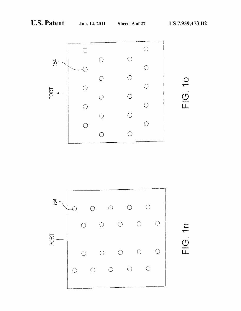
FIG. 1n is a plan view of the terminal arrangement of the connector assembly of FIG. 1 (GBE).
FIG. 1o is a plan view of the terminal arrangement of the connector assembly of FIG. 1 i (10/100).
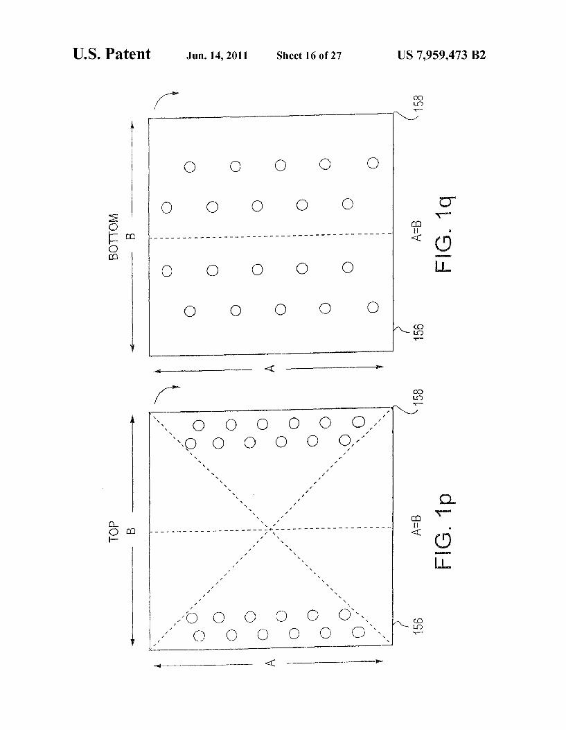
FIG. 1p is a top plan view of the terminal arrangement of yet another embodiment of the electronics insert assembly, showing multiple upper terminal arrays.
FIG.1q is a bottom plan view of the insert assembly of FIG. 1p showing the “universal GBE and 10/100 pin configura tions.
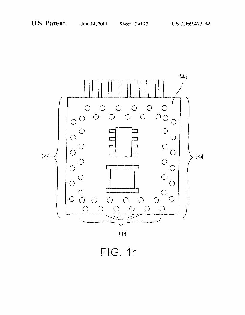
FIG. 1r is a top plan view of an exemplary upper substrate configuration useful with the insert assembly of FIGS. 1p and

US 7,959,473 B2
FIG. 1s is a rear perspective view of another exemplary embodiment (2x1, for Gigabit Ethernet) of the connector assembly according to the present invention.
FIG. 2 is a rear perspective view of a second exemplary embodiment (single port) of the connector assembly accord ing to the present invention.
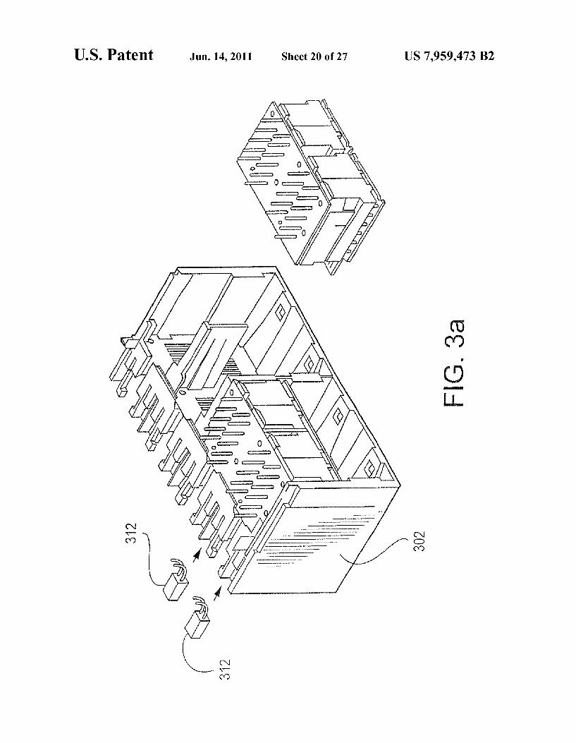
FIGS. 3a–3d are various rear perspective views of another exemplary embodiment (2x4) of the connector assembly according to the present invention, including one configura tion of indicating means.
FIG. 4 is a side cross-sectional view of yet another exem plary embodiment (2x4) of the connector assembly according to the present invention (shown unshielded, and with elec tronics inserts and various components removed for clarity), including another configuration of indicating means.
FIG. 5 is a logical flow diagram illustrating one exemplary embodiment of the method of manufacturing the connector assembly of the present invention.
DETAILED DESCRIPTION OF THE PREFERRED EMBODIMENT
Reference is now made to the drawings wherein like numerals refer to like parts throughout.
It is noted that while the following description is cast primarily in terms of a plurality of RJ-type connectors and associated modular plugs of the type well known in the art, the present invention may be used in conjunction with any num ber of different connector types. Accordingly, the following discussion of the RJ connectors and plugs is merely exem plary of the broader concepts. As used herein, the terms "electrical component” and
'electronic component” are used interchangeably and refer to components adapted to provide some electrical function, including without limitation inductive reactors ("choke coils'), transformers, filters, gapped core toroids, inductors, capacitors, resistors, operational amplifiers, and diodes, whether discrete components or integrated circuits, whether alone or in combination. For example, the improved toroidal device disclosed in Assignee's U.S. patent application Ser. No. 09/661,628 entitled “Advanced Electronic Microminia ture Coil and Method of Manufacturing filed Sep. 13, 2000 (now issued as U.S. Pat. No. 6,642.827), which is incorpo rated herein by reference in its entirety, may be used in con junction with the invention disclosed herein. As used herein, the term 'signal conditioning or “condi
tioning shall be understood to include, but not be limited to, signal Voltage transformation, filtering, current limiting, Sam pling, processing, and time delay. As used herein, the term “port pair refers to an upper and
lower modular connector (port) which are in a Substantially over-under arrangement; i.e., one port disposed substantially atop the other port, whether directly or offset in a given direction. As used herein, the term “interlock base' refers generally
to, without limitation, a structure such as that disclosed in U.S. Pat. No. 5,015,981 to Lint, et al. issued May 14, 1991 entitled “Electronic microminiature packaging and method”. U.S. Pat. No. 5,986,894 to Lint, et al. issued Nov. 16, 1999
5
10
15
25
30
35
40
45
50
55
entitled “Microelectronic component carrier and method of 60 its manufacture', U.S. Pat. No. 6,005,463 to Lint, et al. issued Dec. 21, 1999 entitled “Through-hole interconnect device with isolated wire-leads and component barriers, U.S. Pat. No. 6,395,983 to Gutierrez issued May 28, 2002 entitled “Electronic packaging device and method’, or U.S. Pat. No. 6,593,840 to Morrison, et al. issued Jul. 15, 2003 entitled "Electronic packaging device with insertable leads and
65
10 method of manufacturing, each of the foregoing incorpo rated herein by reference in its entirety.
Multi-Port Embodiment
Referring now to FIGS. 1-1o, a first embodiment of the connector assembly of the present invention is described. As shown in FIG. 1, the assembly 100 generally comprises a connector housing element 102 having a plurality of indi vidual connectors 104 formed therein. Specifically, the con nectors 104 are arranged in the illustrated embodiment in side-by-side row fashion within the housing 102 such that two rows 108, 110 of connectors 104 are formed, one disposed atop the other ("row-and-column). The front walls 106a of each individual connector 104 are further disposed parallel to one another and generally coplanar, Such that modular plugs may be inserted into the plug recesses 112 formed in each connector 104 simultaneously without physical interference. The plug recesses 112 are each adapted to receive one modu lar plug (not shown) having a plurality of electrical conduc tors disposed therein in a predetermined array, the array being so adapted to mate with respective conductors 120a present in each of the recesses 112 thereby forming an electrical con nection between the plug conductors and connector conduc tors 120a, as described in greater detail below. The rows 108, 110 of the embodiment of FIG. 1 are ori
ented in mirror-image fashion, Such that the latching mecha nism for each connector 104 in the top row 108 is reversed or mirror-imaged from that of its corresponding connector in the bottom row 110. This approach allows the user to access the latching mechanism (in this case, a flexible tab and recess arrangement of the type commonly used on RJ modular jacks, although other types may be substituted) of both rows 108, 110 with the minimal degree of physical interference. It will be recognized, however, that the connectors within the top and bottom rows 108, 110 may be oriented identically with respect to their latching mechanisms. Such as having all the latches of both rows of connectors disposed at the top of the plug recess 112, if desired. The connector housing element 102 is in the illustrated
embodiment electrically non-conductive and is formed from a thermoplastic (e.g. PCT Thermex, IR compatible, UL94V 0), although it will recognized that other materials, polymer or otherwise, may conceivably be used. An injection molding process is used to form the housing element 102, although other processes may be used, depending on the material cho sen. The selection and manufacture of the housing element is well understood in the art, and accordingly will not be described further herein. As shown in FIGS. 1a-1b, the connector assembly may
also be shielded with, interalia, an external tin or alloy noise shield 107 of the type well known in the art, or of the con figuration described in greater detail Subsequently herein. A plurality of grooves 122 which are disposed generally
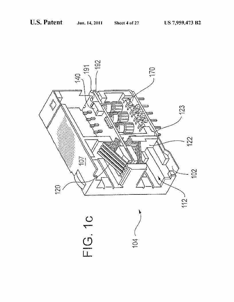
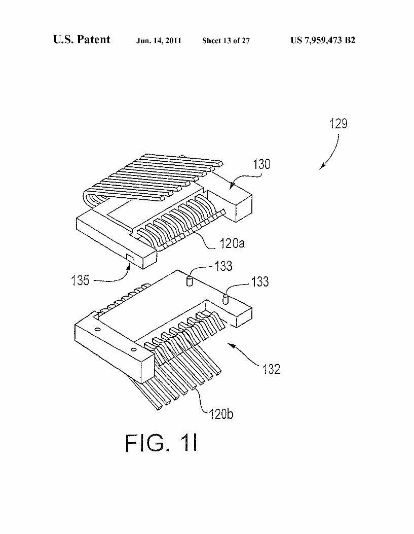
parallel and oriented vertically within the housing 102 are formed generally within the recess 112 of each connector 104 in the housing element 102. The grooves 122 are spaced and adapted to guide and receive the aforementioned conductors 120 used to mate with the conductors of the modular plug. The conductors 120 are formed in a predetermined shape and held within one of a plurality of conductor or terminal insert assemblies 129 each formed of two sub-assemblies 130, 132 (FIG. 11), the latter also being received within the housing element 102 as shown in FIGS. 1c and 1 m. Specifically, the housing element 102 includes a plurality of cavities 134 formed in the back of respective connectors 104 generally adjacent to the rear wall of each connector 104 and extending

US 7,959,473 B2 11
forward into proximity of the recesses 112, each cavity 134 being adapted to receive the terminal insert assemblies 129 (either one, two, or more, as described below in various embodiments). The first conductors 120a of the substrate/ component assemblies 129 are deformed such that when the assemblies 129 are inserted into their respective cavities 134, the upper conductors 120a are received within the grooves 122., maintained in position to mate with the conductors of the modular plug when the latter is received within the plug recess 112, and also maintained in electrical separation by the separators 123 disposed between and defining the grooves 122. When installed, the respective terminal inserts 129 are in a Substantially juxtaposed arrangement (see FIG. 1e).
Each cavity is further adapted to receive an electronics insert assembly 150 of the type generally shown in FIG. 1f. It will be recognized that the term “electronics' as used herein does not require that any electronic components or electron ics be disposed on or within the assembly 150, albeit a pre ferred construction. Specifically, the connector assembly of the present invention may be practiced with no electronic components whatsoever for one or more ports if desired.
Referring now to FIGS. 1d and 1f1 k, exemplary configu rations of the (electronics) insert elements 150 are described in detail. As shown best in FIGS. 1d and 1.f. the exemplary embodiment of the connector assembly 100 includes a plu rality of insert assemblies 150 that are received substantially within the rear cavities 134 of the housing 102. These assem blies include an upper substrate 140 and a plurality of upper terminals 152 and lower terminals 154, the latter which in the illustrated embodiment are separate components, although it will be recognized that they may be made unitary if desired (e.g., in a one-piece “pass through configuration which traverses the thickness of the insert element body 151). Alter natively, one or both sets ofterminals (or even individual ones of the terminals within a set) can be configured in a different fashion, such as for example using a Surface mount technique (e.g., akin to a ball grid array or BGA semiconductor pack age). It will be appreciated that the terms “upper and “lower as used herein are meant in a completely relative sense, and are not in any way limiting or indicative of any preferred orientation. For example, where the connector assembly is installed on the underside of a substantially horizontal moth erboard, the “upper terminals would actually be disposed below the “lower terminals.
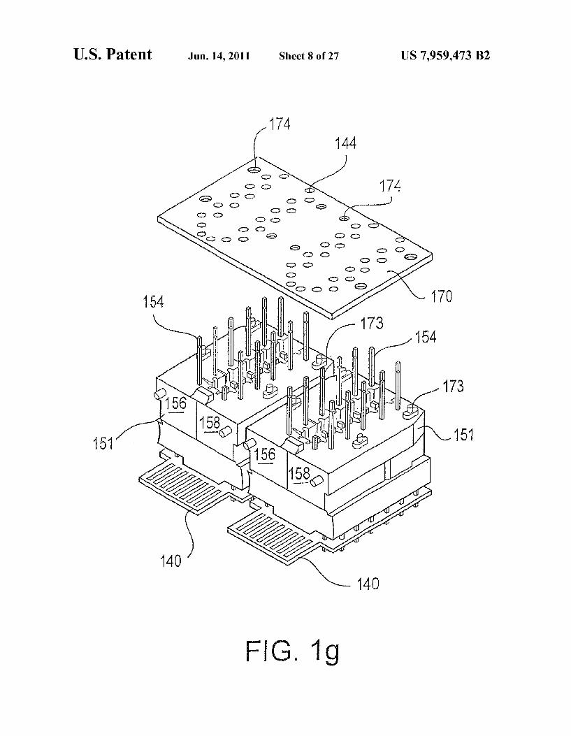
The exemplary terminals shown in FIGS. 1d and 1f1 k are insert-molded into the two insert body elements 156, 158 which form the insert element body 151, although these may be fixed using an adhesive, inserted after molding, use of “staking, etc. Furthermore, the two body elements 156,158 may beformed using any number of processes including, e.g., injection molding or transfer molding. The upper substrate 140 includes a plurality of apertures
144 to receive the upper terminals 152, and may be populated on one or both Surfaces with any manner of electronic com ponents (whether discrete components such as resistors, capacitors, etc. or integrated circuits), conductive traces, etc. The upper substrate 140 also includes a distal portion 145 which has a series (e.g., eight) conductive traces 146 disposed on its Surfaces (both upper and lower) So as to cooperate with corresponding ones of the rear-most ends of the conductors 120a, 120b of the terminal insert assembly 129, as shown best in FIG. 1 m. The upper substrate 140 may be a single-layer board, or alternatively comprise a multi-layer board having a plurality of vias or other electrical pathways formed thereinas is well known in the electronic arts. When assembled, each individual insert assembly 150 is
'ganged with its adjacent port-pair neighbor (if any) as
10
15
25
30
35
40
45
50
55
60
65
12 shown in FIG. 1d. Specifically, the individual assemblies 150 are mated to a common lower substrate 170 using a set of complementary frictional or snap pins 173 on the insert body elements 156, 158 and holes 174 formed in the lower sub strate, although other means (such as via Soldering the lower terminals 154, adhering the assemblies 150 to the substrate 170, heat staking, or another such approaches) may be used if desired. It will be recognized, however, that other configura tions may be used, including without limitation: (i) having each insert assembly 150 and its upper and lower substrates comprise an individual unit, thereby making each assembly 150 for each port-pair independently removable; (ii) using both common upper and lower Substrates for each pair of insert assemblies 150; or (iii) using common upper and/or lower substrates for more than two insert assemblies 150 (such as where all four inserts 150 of a 2x4 configuration are commonly "ganged onto one common lower substrate 170 that is received in one large cavity 134 formed in the back end of the connector housing 102. Several other approaches are possible, each being readily recognized and implemented by those of ordinary skill provided the present disclosure. The lower substrate(s) 170 are disposed in the illustrated
embodiment on the bottom face of the connector assembly 100 adjacent to the PCB or external device to which the assembly 100 is ultimately mounted. Each substrate 170 com prises, in the illustrated embodiment, at least one layer of fiberglass, although other arrangements and materials may be used. The substrate 170 further includes a plurality of con ductor perforation arrays formed at predetermined locations on the substrate 170 with respect to the lower conductors 154 of each insert assembly 150 such that when the connector assembly 100 is fully assembled, the conductors 154 pen etrate the substrate 170 via respective ones of the aperture arrays. This arrangement advantageously provide mechanical stability and registration for the lower conductors 154, as well as stability for the insert assemblies 150. One salient attribute of the present invention relates to its
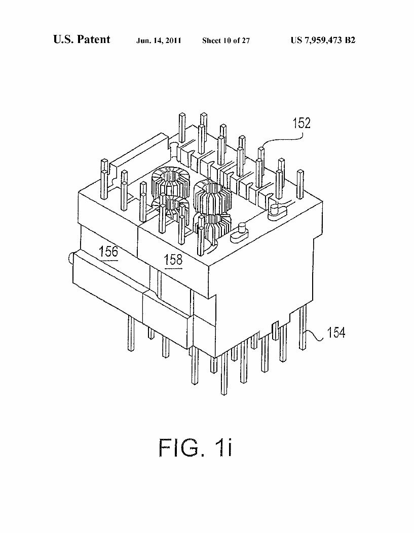
ability to be used in a number of different configurations and/or applications. Specifically, as shown in FIGS. 1f1.h and 1i, the connector assembly can include lower terminals 154 disposed in one or multiple Substantially parallel rows run ning fore-to-aft (i.e., along lines running from the front face 106 to the rear of the housing 102), such as is typically used in gigabit Ethernet (GBE) or other applications; see FIG. 1n for a plan view of this lower terminal configuration. Alterna tively, as shown in FIGS. 1n, 1k, and 10, the insert assembly 150 can be configured with the lower terminals 154 disposed in one or more Substantially parallel rows disposed perpen dicular to those previously described, as is typically used in many 10/100 Ethernet applications. Myriad other configura tions of the lower terminals (including mixtures of the two approaches described above) can be employed as desired, Such as for custom terminal pin-outs.
Notably, the illustrated embodiments previously described also use a common configuration for the upper terminals 152 of the insert assemblies 150, so that the upper substrate 140 which is disposed atop the insert assembly 150 need not be changed for each different insert assembly configuration. Hence, the exemplary connector assembly 100 can be con figured as either a GBE device, a 10/100 device, or otherwise simply by inserting a different configuration of the insert assembly 150 within the housing 102. This simplifies manu facturing, since the housings 104, terminal inserts 129, upper substrates 140, noise shields, etc. are identical for each dif ferent variant; the only change relates to the insert assembly 150 and the lower substrate(s) 170.

US 7,959,473 B2 13
In fact, the lower substrates 170 may be either (i) com pletely obviated in certain embodiments or applications, or (ii) made also to be “universal' by having perforations for both GBE and 10/100 pin-outs such that the same lower Substrate 170 can be used with either insert element 150. This can be accomplished for example by aligning the various components including the lower terminals and insert bodies 156, 158 to meet the pin-out requirements, and then placing the perforations in the lower substrate 170 such that they both meet both of the pin-outs, and utilize at least some of the same perforations for either application.
It will also be recognized that a given insert assembly 150 can itself be made “universal'. In one embodiment of the invention (FIGS. 1p and 19), each insert assembly body 156, 158 is configured such that it is effectively square, and there fore can be inserted into the housing 102 in either a first or second orientation (each orientation being rotated 90-degrees from the other). The upper substrate 140 (FIG. 1r) is designed to remain in the same orientation regardless of the orientation of the insert assembly body, and accordingly has two sets of substantially identical perforations 144 formed therein such that the upper terminals 152 of the insert element body can be received in one set or another of the perforations regardless of the orientation of the insert body. The lower terminals 154 (FIG. 19) are accordingly disposed in either the GBE orien tation or the 10/100 (or whatever other pin-outs of signifi cance are chosen) depending on how the insert body is inserted into the housing.
It is noted also that the electronics package utilized within the insert assembly 150 can be made to accommodate both variants (i.e., GBE or 10/100) by the use of additional or extra electronic components (e.g., magnetics) to account for either use, and/or by making the electronics serve a dual-purpose where possible. Alternatively, individual ones of the insert assemblies 150 designed for GBE applications can be wired/ equipped one way, and those destined for 10/100 applications wired/equipped another, since even the use of “universal insert assembly body elements 156,158 reduces manufactur ing costs since only one type of insert assembly (albeit wired and equipped differently) is needed.
In the illustrated embodiments, one or more types of elec tronic components are disposed within the interior cavity 180 formed within each insert assembly 150, including e.g., choke coils, transformers, etc. (see FIG. 1j). These compo nents have their wires in electrical communication with one or more of the upper and lower terminals 152, 154 of the assembly 150. Such as via wire-wrapping, soldering, welding, or the like. A plurality of wire channels 184 are also provided to aid in wire routing and separation. The terminals 152, 154 may also be notched as is well known in the art to further facilitate bonding of the wires thereto. The electronic com ponents may also be encapsulated within a potting compound or encapsulant Such as epoxy or silicone gel, if desired. The two body elements 156, 158 are snapped together using a pin-hole arrangement as shown in FIG. 1j, although it will be appreciated that other mechanisms may be used Such as adhe sives, thermal bonding, etc. Furthermore, it will be recog nized that the insert body may be formed as a unitary com ponent (e.g., with an opening to insert the various electronic components, or as a sold block of plastic or encapsulant) rather than in “halves” as shown.
In another embodiment, an interlock base or comparable component is used inside of the cavity 180 for, inter alia, additional electrical separation.
In yet another embodiment (not shown), the insert assem bly 150 can be split top-and-bottom, such that the two body elements 156, 158 are disposed in substantially over/under
5
10
15
25
30
35
40
45
50
55
60
65
14 arrangement. The upper terminals 152 are hence insert molded or otherwise disposed within the upper body element, while the lower terminals 154 are formed or disposed in the lower body element. The terminal insert assemblies 129 are retained within their
cavities 134 substantially by way of friction with the housing element 102, although other methods and arrangements may be substituted with equal success. The illustrated approach allows for easy insertion of the completed terminal assem blies 129 into the housing 102, and subsequent selective removal if desired.
FIG.1 lbest shows the construction of the terminal assem blies 129, comprising the two sub-assemblies 130, 132. In the illustrated embodiment, the two sub-assemblies are held together by at least a friction locating pin 133 or heat stake arrangement, although other arrangements readily apparent to those of ordinary skill can be used (such as adhesives). Alternatively, the two sub-assemblies can be formed as one unitary component if desired. The embodiment of FIG. 11 uses insert-molded terminals
(conductors) 120 of the type well known in the connector arts, although other arrangements can be used, including inserting the unformed leads into the sub-assemblies 130, 132 after formation and then Subsequently forming the conductors 120.
It will also be recognized that separators or EMI shields can be disposed between the conductor sets of any given terminal insert assembly 129 (or between adjacent ones of the juxta posed assemblies 129) so as to minimize electrical noise and cross-talk between the conductor sets 120a, 120b and/or between other components. For example, the multi-dimen sional shielding apparatus and techniques described in U.S. Pat. No. 6,585,540 to Gutierrez, et al. issued Jul. 1, 2003 entitled “Shielded microelectronic connector assembly and method of manufacturing and incorporated herein by refer ence in its entirety may be used consistent with the present invention, with proper adaptation. Other shielding configura tions may also be used, the foregoing being but one option. Furthermore, other techniques well known in the electronic arts for minimizing EMI and/or cross-talk may be used con sistent with the invention if desired. The inserts 129 are also provided with optional locking
mechanisms 135 to lock them into their channels within the housing 102, although this can also be accomplished using friction, heat staking, or another means.
In the illustrated embodiment, the two sets of conductors 120a, 120b for each terminal insert 129 are disposed relative to one another in Substantially mirror image, although this is by no means a requirement. Use of mirror-image sets of conductors can significantly simplify the manufacturing pro cess, since formation and handling of heterogeneous conduc tor configurations are obviated. However, there are applica tions where it may be desirable to use Such heterogeneous configurations, such as where the two connectors in the port pair are heterogeneous, or where the internal structure of the assembly 100 dictates such a configuration.
It is further noted that while the embodiment of FIGS. 1-1q comprises two rows 108, 110 of four connectors 104 each (thereby forming a 2 by 4 array of connectors), other array configurations may be used. For example, a 2 by 2 array comprising two rows of two connectors each could be Sub stituted. Alternatively, a 2 by 8 arrangement could be used. A 2x1 array (FIG. 1s) may also be used. As yet another alterna tive, an asymmetric arrangement may be used. Such as by having two rows with an unequal number of connectors in each row (e.g., two connectors in the top row, and four con nectors in the bottom row). The modular plug recesses 112 (and front faces 106a) of each connector also need not nec

US 7,959,473 B2 15
essarily be coplanaras in the embodiment of FIG. 1. Further more, certain connectors in the array need not have lower Substrates/electronic components, or alternatively may have components disposed in the insert assemblies 150 and/or on the substrates different than those for other connectors in the same array. As yet another alternative, the connector configurations
within the connector housing may be heterogeneous or hybridized. For example, one or more of the upper/lower row port pairs may utilize configurations which are different from those used for other port pairs. Such as where the electronics package for one port-pair is different than that for another port-pair within the same connector assembly 100. Alterna tively, individual ports within a pair can have heterogeneous configuration. As yet another alternative, port-pairs can be intermixed, such as where two of the four insert assemblies 150 used in the 2x4 configuration of FIG. 1 are configured for GBE, while the other two are configured for 10/100 or another standard. Many other permutations are possible consistent with the
invention; hence, the embodiments shown herein are merely illustrative of the broader concept.
Single Port Embodiment
Referring now to FIG. 2, another embodiment of the con nector assembly of the present invention is described. As shown in FIG. 2, the assembly 200 generally comprises a connector housing element 202 having one modular plug receiving connector 204 formed therein. The front wall 206a of the connector 204 is further disposed generally perpen dicular or orthogonal to the PCB surface (or other device) to which the connector assembly 200 is mounted, with the latch mechanism located away from the PCB, such that modular plugs may be inserted into the plug recess 212 formed in the connector 204 without physical interference with the PCB. The plug recess 212 is adapted to receive one modular plug (not shown) having a plurality of electrical conductors dis posed therein in a predetermined array, the array being so adapted to mate with respective conductors 220a present in the recess 212 thereby forming an electrical connection between the plug conductors and connector conductors 220a. This embodiment can be thought of in a broad sense as being only one port of only the lower portion of the connector 100 of FIG.1m. Specifically, the upper substrate 240 has traces, components, etc. disposed on its lower Surface in order to conserve vertical profile (although this is not a requirement), and the substrate 240 disposed atop a streamlined body 251 similar to the insert assembly 150 of the connector 100 of FIG. 1. Specifically, since the connector 200 has only one port, the signal conditioning/electronics requirements are proportionately less, and hence the insert assembly 250 (and cavity 234) can be made Smaller and more compact if desired. Also, reduced height upper terminals can be used to reduce vertical profile, or alternatively another interface mechanism (such as BGA or the like) can be employed. Hence, the connector assembly 200 of FIG. 2 can optionally have the form factor (and footprint) of a conventional RJ or similar jack if desired.
Referring now to FIGS. 1-1c and 1f another aspect of the invention is described. Specifically, as best shown in the foregoing Figures, the connector assembly 100 optionally includes an external noise shield 107 disposed substantially around the exterior of the connector 100. The exemplary shield 107 comprises a two piece construction (although more or less pieces may be used), and includes a plurality of “clips' 191 formed in the rear of the shield (see FIGS. 1a and
5
10
15
25
30
35
40
45
50
55
60
65
16 1c). These clips 191 are adapted to connect electrically with corresponding pads or contacts 192 on the upper Substrate 140 when the rear shield component is placed over the rear of the connector housing 102. The contacts 192 are electrically connected to a capacitor disposed on, e.g., the upper Sub strate, thereby providing a low impedance path to ground through the shield. These clips 191 and contacts 192 may be purely a friction fit, soldered or otherwise mechanically bonded, or both, as desired. As shown in FIG. 1a, the rear shield element ground tabs
193 slide between the lower Substrate 170 and the insert assembly 150. Also, the front tabs 194 of the shield (FIG.1b) slide within grooves formed on the bottom of the housing and under the lower substrate 170 as well, thereby securing the shield 170 to the housing. These tabs are also optionally connected electrically to the lower substrate 170 (e.g., contact pads formed on the top or bottom surface thereof) in order to provide a ground connection similar to the for the clips 191 previously discussed. Such connection may be frictional, via a bonding process such as soldering, or otherwise.
It is noted that the aforementioned shield can also be adapted to accommodate various component packages dis posed at the rear of the connector assembly, for example the illuminating means shown in FIGS. 3a–3d, described subse quently herein.
Connector Assembly with Light Sources
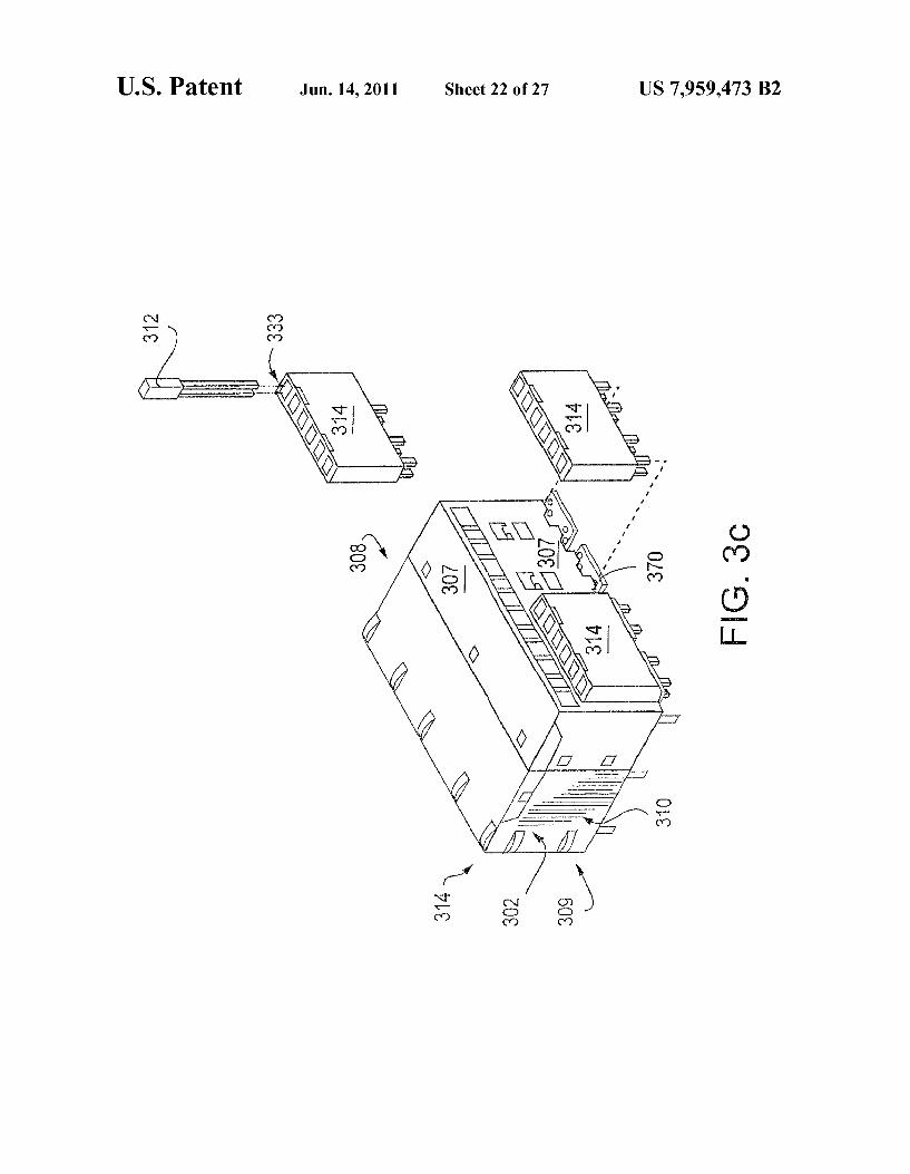
Referring now to FIGS. 3 and 4, yet other embodiments of the connector assembly of the present invention are described. As shown in FIGS. 3a–3d, another embodiment of the
connector 300 includes light sources comprising a light pipe arrangement. Light pipes are generally known in the art; however, the arrangement of the present invention adapts the light pipe to the connector configurations otherwise disclosed herein. Specifically, as shown in FIGS. 3a–3d, the illustrated embodiment comprises a two-row connector assembly (i.e., at least one upper row connector and at least one lower row connector) having one or more light pipe assemblies 310 associated therewith. For the upper row connector 302, the light pipe assembly 310 comprises an optically conductive medium 304 adapted to transmit the desired wavelength(s) of light energy from a light source 312, in this case an LED. The LED 312 is disposed within a carrier element 314 disposed proximate to the back Surface of the connector assembly which is adapted and sized to receive the LED(s). The carrier 314 can accommodate a number of LEDs or similar sources as shown. The LED conductors are mated to the lower sub strate 370, which projects somewhat out the back of the connector assembly 300 as shown best in FIG. 3e. Note that the LED recesses 333 within the carrier 314 may
also be coated internally with a reflective coating of the type well known in the art to enhance the reflection of light energy radiated by the LED during operation into the interior face of the optical medium 304. The optically conductive medium may comprise a single unitary light path from the interior face 316 to the viewing face 318, or alternatively a plurality of abutted or joined optically transmissive segments. As yet another approach, one or more 'ganged’ optical fibers (e.g., single mode or multimode fibers of the type well known in the optical networking arts) may be used as the optical medium. As yet another alternative, a Substantially prismatic device may be used as the optical medium 304, especially if substan tial chromatic dispersion is desired. The optical medium may be removably retained within the connector assembly hous ing, or alternatively fixed in place (such as by being molded
US 7,959,473 B2 17
within the housing, or retained using an adhesive or friction), or any combination of the foregoing as desired. The light pipe assembly 310 is disposed within the upper
portion of the connector housing within a channel formed therein. It will be noted that due to the longer optical “run” and greater optical losses associated with this second optical medium, the size/intensity of the LED 312, and/or the optical properties or dimensions of the medium 304, may optionally be adjusted so as to produce a luminosity Substantially equivalent to that associated with the LEDs for the bottom OW.
Also, the LEDs for the bottom row can be used with a lens, prism, or optical medium (albeit much shorter in length than that for the upper row of connectors) if desired in order to provide a homogeneous appearance for the indicators of the top and bottom rows of connectors.
It will also be appreciated that while the embodiment of FIG.3a-3d is shown with an exemplary external noise shield 307, this shield is optional, or may comprise another configu ration if desired, including one which is external to the LEDs and optical indicators. Placing of the LEDs outside of the noise shield also helps mitigate interference between the LEDs and the signal paths/electronic components within the COnnectOr.
It can also be appreciated that while the foregoing embodi ment is described interms of a two-row connector device, the light pipe assemblies of the invention may also be imple mented in devices having other numbers of rows, such as for example with a 1xN device.
In another variant, the light pipe configuration of the type shown in co-owned and co-pending U.S. patent application Ser. No. 10/246,840 filed Sep. 18, 2002 entitled "Advanced Microelectronic Connector Assembly and Method of Manu facturing (now issued as U.S. Pat. No. 6,962.511), incorpo rated herein by reference in its entirety, can be used consistent with the invention in order to provide indication functionality.
In the alternate embodiment of FIG. 4, the connector assembly 400 comprises a plurality of light sources 403, presently in the form of light emitting diodes LEDs of the type well known in the art. The light sources 403 are used to indicate the status of the electrical connection within each connector, as is well understood. The LEDs 403 of the embodiment of FIG. 4 are disposed at the bottom edge 409 of the bottom row 410 and the top edge 414 of the top row 408, two LEDs per connector, adjacent to and on either side of the modular plug latch mechanism, so as to be visible from the front face of the connector assembly 400. The individual LEDs 403 are, in the present embodiment, received within recesses 444 formed in the front face of the housing element 402. The LEDs each include two conductors 411 which run from the rear of the LED to the rear portion of the connector housing element 402 generally in a horizontal direction within lead channels formed in the housing element. The LED conductors 411 are sized and deformed at such an angle towards their distalends such that they can either (i) mate with respective apertures formed on the primary Substrate(s) asso ciated with each modular plug port, the conductors then being in electrical communication with respective second conduc tors disposed at the other end of the primary substrate, (ii) run uninterrupted to the upper Substrate 440 (i.e., one continuous conductor), and penetrate therethrough and emerge from cor responding apertures formed in the Substrate 440, or (iii) run directly from the LED to the PCB/external device without regard to or interaction with the upper Substrate.
Similarly, a set of complementary grooves are provided, Such grooves terminating on the bottom face of the housing 402 coincident with the conductors 411 for the LEDs of the
10
15
25
30
35
40
45
50
55
60
65
18 bottom row of connectors. These allow the LED conductors to be received within their respective recesses 444, and upon emergence from the rear end of the recess 444, be deformed downward to be frictionally received within their respective grooves. The recesses 444 formed within the housing element 402
each encompass their respective LED when the latter is inserted therein, and securely hold the LED in place via friction between the LED 403 and the inner walls of the recess (not shown). Alternatively, a looser fit and adhesive may be used, or both friction and adhesive. As yet another alternative, the recess 444 may comprise only two walls, with the LEDs being retained in place primarily by their conductors 411, which are frictionally received within grooves formed in the adjacent Surfaces of the connector housing. As yet another alternative, the external shield element 107 may be used to provide support and retention of the LEDs within the recesses 444, the latter comprising three-sided channels into which the LEDs 403 fit. Many other configurations for locating and retaining the LEDs in position with respect to the housing element 402 may be used. Such configurations being well known in the relevant art. The two LEDs 403 used for each connector 404 radiate
visible light of the desired wavelength(s). Such as green light from one LED and red light from the other, although multi chromatic devices (such as a “white light' LED), or even other types of light sources, may be substituted if desired. For example, a light pipe arrangement Such as that using an opti cal fiber or pipe to transmit light from a remote source to the front face of the connector assembly 400 may be employed. Many other alternatives such as incandescent lights or even liquid crystal (LCD) or thin film transistor (TFT) devices are possible, all being well known in the electronic arts. The connector assembly 400 with LEDs 403 may further
be configured to include noise shielding for the individual LEDs if desired. Note that in the embodiment of FIG. 4, the LEDs 403 are positioned inside of (i.e., on the connector housing side) of the external noise shield 107 (not shown). If it is desired to shield the individual connectors 404 and their associated conductors and component packages from noise radiated by the LEDs, such shielding may be included within the connector assembly 300 in any number of different ways. In one embodiment, the LED shielding is accomplished by forming a thin metallic (e.g., copper, nickel, or copper-zinc alloy) layer on the interior walls of the LED recesses 444 (or even over the non-conductive portions of LED itself) prior to insertion of each LED. In a second embodiment, a discrete shield element (not shown) which is separable from the con nector housing 402 can be used, each shield element being formed so as to accommodate its respective LED and also fit within its respective recess 444. In yet another embodiment, the external noise shield may be fabricated and deformed within the recesses 444 so as to accommodate the LEDs 403 on the outer surface of the shield, thereby providing noise separation between the LEDs and the individual connectors 404. Myriad other approaches for shielding the connectors 404 from the LEDs may be used as well if desired, with the only constraint being Sufficient electrical separation between the LED conductors and other metallic components on the connector assembly to avoid electrical shorting.
Method of Manufacture
Referring now to FIG. 5, the method 500 of manufacturing the aforementioned connector assembly 100 is described in detail. It is noted that while the following description of the method 500 of FIG. 5 is cast in terms of the multiple port-pair
US 7,959,473 B2 19
connector assembly of FIG. 1, the broader method of the invention is equally applicable to other configurations (in cluding e.g., the single-port embodiment of FIG. 2).
In the embodiment of FIG. 5, the method 500 generally comprises first forming the assembly housing element 102 in 5 step 502. The housing is formed using an injection molding process of the type well known in the art, although other processes may be used. The injection molding process is chosen for its ability to accurately replicate small details of the mold, low cost, and ease of processing.
Next, two conductor sets (120a, 120b) are provided in step 504. As previously described, the conductor sets comprise metallic (e.g., copper or aluminum alloy) strips having a Substantially square or rectangular cross-section and sized to fit within the slots of the connectors in the housing 102. 15
In step 506, the conductors are partitioned into sets; a first set 120a for use with a first connector recess of each port-pair (i.e., within the housing 102, and mating with the modular plugterminals), and a second set 120b for the other port in the port-pair. The conductors are formed to the desired shape(s) using a forming die or machine of the type well known in the art. Specifically, for the embodiment of FIG. 1, the first and second conductor sets 120a, 120b is deformed so as to pro duce the juxtaposed, Substantially coplanar configuration as shown in FIG. 11 and previously described.
In step 508, the first and second conductor sets 120a, 120b are insert-molded within the respective portions of the termi nal insert assembly 129, thereby forming the components shown in FIG. 11. In step 510, the two sub-components of the insert 129 are mated. Such as via Snap-fit, friction, adhesive, thermal bonding, etc.
In step 512, the upper and lower terminals 152, 154 are formed using similar methods to those used for the conduc tors 120a, 120b, although in the illustrated embodiment the upper and lower terminals 152, 154 need not be deformed (i.e., can remain Straight) if desired.
Note also that either or both of the aforementioned con ductor sets may also be notched (not shown) at their distal ends such that electrical leads associated with the electronic components (e.g., fine-gauge wire wrapped around the mag netic toroid element) may be wrapped around the distal end notch to provide a secure electrical connection.
In step 514, the first and second body elements 156,158 of the (electronics) insert assembly 150 are formed, such as via injection or transfer molding. In one embodiment, a high- 45 temperature polymer of the type ubiquitous in the art is used to form the body elements 156, 158, although this is not required, and other materials (even non-polymers) may be used.
Next, the upper substrate 140 is formed and perforated 50 through its thickness with a number of apertures of predeter mined size in step 516. Methods for forming substrates are well known in the electronic arts, and accordingly are not described further herein. Any conductive traces on the sub strate required by the particular design are also added. Such 55 that necessary ones of the conductors, when received within the apertures, are in electrical communication with the traces.
The apertures within the primary Substrate are arranged in two arrays of juxtaposed perforations, one at each end of the Substrate, and with spacing (i.e., pitch) such that their position 60 corresponds to the desired pattern, although other arrange ments may be used. Any number of different methods of perforating the Substrate may be used, including a rotating drill bit, punch, heated probe, or even laser energy. Alterna tively, the apertures may beformed at the time of formation of 65 the Substrate itself, thereby obviating a separate manufactur ing step.
10
25
30
35
40
20 Next, the lower substrate 170 is formed and is perforated
through its thickness with a number of apertures of predeter mined size in step 518. The apertures are arranged in an array of bi-planar perforations which receive corresponding ones of the lower conductors 154 therein, the apertures of the lower Substrate acting to register and add mechanical stability to the lower set of conductors. Alternatively, the apertures may be formed at the time of formation of the substrate itself.
In step 520, one or more electronic components, such as the aforementioned toroidal coils and Surface mount devices, are next formed and prepared (if used in the design). The manu facture and preparation of such electronic components is well known in the art, and accordingly is not described further herein. The relevant electronic components are then mated to the
upper substrate 140 in step 522. Note that if no components are used, the conductive traces formed on/within the primary substrate will form the conductive pathway between the first and second sets of conductors 120 and respective ones of the upper conductors 152. The components may optionally be (i) received within corresponding apertures designed to receive portions of the component (e.g., for mechanical stability), (ii) bonded to the substrate such as through the use of an adhesive or encapsulant, (iii) mounted in “free space' (i.e., held in place through tension generated on the electrical leads of the component when the latter are terminated to the substrate conductive traces and/or conductor distal ends, or (iv) main tained in position by other means. In one embodiment, the Surface mount components are first positioned on the primary Substrate, and the magnetics (e.g., toroids) positioned there after, although other sequences may be used. The components are electrically coupled to the PCB using a eutectic solder re-flow process as is well known in the art.
In step 524, the remaining electrical components are dis posed within the cavity of the insert assembly 150 and wired electrically to the appropriate ones of the upper and lower terminals 152, 154. This wiring may comprise wrapping, soldering, welding, or any other Suitable process to form the desired electrical connections.
In step 526, the two completed body elements 156,158 are mated (e.g., Snap-fit, bonded, etc.) So as to form the body 151 of the insert assembly 150. The electronic components of the assembly 150 are then optionally secured with silicone or other encapsulant (step 528), although other materials may be used. This completes the insert assembly sub-structure 153.
In step 530, the assembled upper substrate with SMT/ magnetics is then mated with the insert assembly Sub-struc ture 153 and its components, specifically such that the upper terminals 152 are disposed in their corresponding apertures of the substrate 140. The terminals 152 are then bonded to the Substrate contacts such as via soldering or welding to ensure a rigid electrical connection for each. The completed insert assembly may be electrically tested to ensure proper opera tion if desired.
In step 532, two of the completed insert assemblies 150 are mated to a common lower substrate 170 and bonded thereto if desired to as to form a Substantially rigid insert structure.
In step 534, the terminal insert assemblies 129 previously formed are inserted within their grooves formed in the cavi ties 134 of the housing 102, and snapped into place.
Next, the completed insert structures of step 532 are inserted into the housing and Snapped into place, thereby completing the (unshielded) connector assembly 100 (step 536).
Alternatively, in step 534, the terminal insert assemblies 129 can be mated directly to the upper substrate; e.g., by inserting the appropriate end of the upper substrate 140
US 7,959,473 B2 21
between the conductor ends 120a, 120b and bonding the latter to their corresponding conductive pads/traces on the Surface of the Substrate 140. Such as via a soldering or welding pro cess. The assembled components (i.e. insert assemblies 150 with attached lower substrate 170 and terminal insert assem bly 129) can then be inserted as a unit into the housing perstep 536.
Lastly, in step 538, the external noise shield (if used) is fitted onto the assembled connector 100, and the various ground straps and clips as previously described positioned so as to provide grounding of the noise shield.
With respect to the other embodiments described herein (i.e., single connector housing, connector assembly with LEDs or light pipes, etc.), the foregoing method may be modified as necessary to accommodate the additional com ponents. Such modifications and alterations will be readily apparent to those of ordinary skill, given the disclosure pro vided herein.
It will be recognized that while certain aspects of the inven tion are described in terms of a specific sequence of steps of a method, these descriptions are only illustrative of the broader methods of the invention, and may be modified as required by the particular application. Certain steps may be rendered unnecessary or optional under certain circum stances. Additionally, certain steps or functionality may be added to the disclosed embodiments, or the order of perfor mance of two or more steps permuted. All Such variations are considered to be encompassed within the invention disclosed and claimed herein.
While the above detailed description has shown, described, and pointed out novel features of the invention as applied to various embodiments, it will be understood that various omis sions, Substitutions, and changes in the form and details of the device or process illustrated may be made by those skilled in the art without departing from the invention. The foregoing description is of the best mode presently contemplated of carrying out the invention. This description is in no way meant to be limiting, but rather should be taken as illustrative of the general principles of the invention. The scope of the invention should be determined with reference to the claims.
What is claimed is: 1. A connector assembly comprising: a connector housing comprising a plurality of plug-receiv
ing recesses and at least one rear cavity; a plurality of terminal insert assemblies each comprised of
a Substantially mirror imaged pair of terminal inserts Such that a given one of the plurality of terminal insert assemblies is received at least partly within at least two of the plug-receiving recesses; and
a plurality of insert assemblies, each said insert assembly comprising: a top Substrate having a plurality of electrically conduc
tive pathways associated therewith, and at least one electronic component disposed substantially thereon, said top Substrate further comprising a plurality of terminal apertures;
a pair of insert body elements comprised of an electronic component receiving space, each of said body ele ments comprising: a plurality of upper conductive terminal portions; a plurality of lower conductive terminal portions; and a plurality of channels that run between the electronic
component receiving space and at least a portion of the lower conductive terminal portions;
wherein said plurality of channels allow for the routing of wire between the electronic component receiving space
5
10
15
25
30
35
40
45
50
55
60
65
22 and the lower conductive terminal portions internal to an outer periphery formed by mated pairs of insert body elements.
2. The connector assembly of claim 1, wherein said assem bly is adapted to receive either of two variants of said insert assemblies without altering the area of an external Substrate consumed by said connector assembly when said connector assembly is mounted on said external Substrate.
3. The connector assembly of claim 2, wherein said hous ing is capable of accommodating a plurality of different con figurations of said insert assemblies both simultaneously and alternatively.
4. The connector assembly of claim3, wherein said plural ity of different configurations comprise at least: (i) a gigabit Ethernet (GBE) configuration, and (ii) an Ethernet 10/100 Mbps configuration.
5. The connector assembly of claim 1, wherein: said housing is capable of accommodating at least two
different configurations of said insert assemblies alter natively without adaptation of the housing:
said at least two different configurations comprise at least: (i) a gigabit Ethernet (GBE) configuration, and (ii) an Ethernet 10/100 Mbps configuration; and
said plurality of plug receiving recesses comprise at least an upper row and lower row of recesses, each of said recesses of said at least upper row configured to receive an RJ-45 modular plug in a first orientation, and each of said recesses of said at least lower row configured to receive an RJ-45 modular plug in a second orientation, said second orientation being a substantial mirror image of said first orientation.
6. The connector assembly of claim 5, further comprising at least one indicator assembly adapted to provide one or more indications visible from a front face of said housing, said at least one indicator assembly comprising at least two at least partly arcuate light pipes, at least two light sources corresponding to said at least two light pipes, and at least one optical isolation element that Substantially isolates the light from a first of said at least two light sources from being carried by a one of said light pipes associated with another of said at least two light sources.
7. The connector assembly of claim 1, further comprising a bottom substrate, said bottom substrate comprised of a plu rality of lower conductive terminal portion apertures and at least one layer of a non-conductive material upon which a layer of a metallic shielding material is disposed.
8. The connector assembly of claim 7, wherein said layer of a metallic shielding material is not present immediately adja cent each of said apertures.
9. The connector assembly of claim 7, wherein first and second ones of said insert assemblies are ganged together in pairs by being mated together with respective common bot tom Substrates.
10. The connector assembly of claim 9, wherein the top Substrate includes a distal portion comprised of a series of conductive traces disposed on both an upper and a lower Surface of said top Substrate.
11. The connector assembly of claim 10, wherein said terminal insert assemblies are mated to said series of conduc tive traces.
12. The connector assembly of claim 11, wherein said terminal insert assemblies are mated to said series of conduc tive traces via a Surface mounted connection.

US 7,959,473 B2 23
13. A connector assembly comprising: a connector housing comprising a plurality of plug-receiv
ing recesses and at least one cavity, said at least one cavity being disposed substantially in a rear portion of said housing:
a plurality of terminal insert structures, each comprising: an upper and a lower plurality of conductors; and an upper and a lower polymer carrier, wherein said upper
and said lower plurality of conductors are disposed at least partly within said upper and said lower polymer carriers respectively, said upper and said lower poly mercarriers being arranged in a substantially mirror image configuration with one another;
wherein said upper and said lower plurality of conduc tors are disposed at least partly within said plug-re ceiving recesses and configured to interface electri cally with respective ones of a modular plug; and
an insert assembly comprising a substrate having a plural ity of electrically conductive pathways and a plurality of electronic components associated therewith, with one or more of said electronic components disposed on said Substrate, said insert assembly further comprised of a plurality of slots on a bottom surface thereof;
wherein said slots permit the electrical connection of one or more electronic components disposed within a cavity associated with said insert assembly to a plurality of conductive terminals disposed external to said cavity;
wherein the connector assembly is further adapted to receive within said cavity alternatively any of at least two variants of said insert assembly.
14. The connector assembly of claim 13, wherein said housing is adapted to accommodate a plurality of different configurations of said insert assemblies both simultaneously and alternatively.
15. The connector assembly of claim 14, wherein said plurality of different configurations comprise at least: (i) a gigabit Ethernet (GBE) configuration, and (ii) an Ethernet 10/100 Mbps configuration.
16. A connector assembly comprising: a connector housing comprising a plurality of plug-receiv
ing recesses and at least one cavity, said at least one cavity being disposed substantially in a rear portion of said housing:
a plurality of terminal insert structures received at least partly within at least two of said plug-receiving recesses simultaneously, each comprising: an upper and a lower plurality of conductors; and an upper and a lower polymer carrier, wherein said upper
and said lower plurality of conductors are disposed at least partly within said upper and said lower polymer carriers respectively, said upper and said lower poly mercarriers being arranged in a substantially mirror image configuration with one another;
wherein said upper and said lower plurality of conduc tors are disposed at least partly within said plug-re ceiving recesses and configured to interface electri cally with respective ones of a modular plug; and
an insert assembly comprising a substrate having a plural ity of electrically conductive pathways and a plurality of electronic components associated therewith with one or more of said electronic components disposed on said Substrate, said insert assembly further comprised of a plurality of slots on a bottom surface thereof, said slots permitting the electrical connection of one or more elec tronic components disposed within a cavity associated with said insert assembly to a plurality of conductive terminals disposed external to said cavity;
5
10
15
25
30
35
40
45
50
55
60
65
24 wherein said Substrate interfaces with a given terminal
insert structure via a surface mounted electrical connec tion, said Surface mounted electrical connection residing on two opposing Surfaces of said Substrate.
17. The connector assembly of claim 16, further compris ing a bottom Substrate, said bottom Substrate comprised of a plurality of lower conductive terminal portion apertures and at least one layer of a non-conductive material upon which a layer of a metallic shielding material is disposed;
wherein said layer of a metallic shielding material is not present immediately adjacent each of said apertures.
18. The connector assembly of claim 16, further compris ing at least one indicator assembly adapted to provide one or more indications visible from a front face of said housing, said at least one indicator assembly comprising at least two at least partly arcuate light pipes, at least two light sources corresponding to respective ones of said at least two light pipes, and at least one optical isolation element that Substan tially isolates the light from a first of said at least two light Sources from being carried by a one of said light pipes asso ciated with another of said at least two light Sources.
19. The connector assembly of claim 18, wherein said at least two light sources are disposed on said connector assem bly Substantially proximate said optical isolation element and proximate in elevation to a bottom Surface of said connector housing.
20. The connector assembly of claim 18, wherein said at least two light pipes, said at least two light sources, and said optical isolation element are removable from said connector assembly Substantially as a single unit.
21. The connector assembly of claim 20, further compris ing a noise shield disposed around at least a portion of the connector housing, and wherein said at least two light pipes, said at least two light sources, and said optical isolation element are removable from said connector assembly Sub stantially as a single unit and without having to remove any portion of said noise shield.
22. A connector assembly comprising: a connector housing comprising a plurality of plug-receiv
ing recesses and Substantially defining an outer perim eter of said connector assembly:
a plurality of terminal insert assemblies, each comprising: a first and a second plurality of conductors; and a first and a second polymer carrier, Supporting at least a
portion of said first and second plurality of conduc tors, respectively;
at least one indicator assembly comprising a plurality of light pipes, at least a portion of said indicator assembly being mounted Substantially along a rear face of said connector assembly and configured to provide one or more indications visible from a front face of said con nector assembly; and
a plurality of insert structures, each of said plurality of insert structures comprising: a Substrate disposed horizontally atop at least two insert body elements, said Substrate having one or more electronic components disposed substantially thereon and a plurality of conductive traces that are configured to interface with at least one of said plurality ofter minal insert assemblies via a Surface mounted elec trical connection;
wherein said at least two insert body elements form an electronic component receiving space, each of said body elements comprising: a top Surface with one or more upper conductive ter
minal portions protruding therefrom, said top Sur face also including a standoff feature;
US 7,959,473 B2 25
a bottom surface with one or more lower conductive terminal portions protruding therefrom; and
a plurality of wire channels with at least a first portion of said wire channels running from said electronic component receiving space to said bottom surface; and
a plurality of wired electronic components, at least a portion having at least two wired ends, said wired electronic components being disposed at least par tially within said electronic component receiving Space;
wherein the wired ends of the wired electronic components collectively are routed to both the upper conductive ter minal portions and the lower conductive terminal por tions; and
wherein said connector assembly is adapted to receive either of two variants of said insert structures in pairs without altering the size of said defined outer perimeter of said connector assembly.
23. The connector assembly of claim 22, wherein said housing is adapted to accommodate a plurality of different configurations of said insert structures both simultaneously and alternatively.
24. The connector assembly of claim 23, wherein said plurality of different configurations comprise at least: (i) a gigabit Ethernet (GBE) configuration, and (ii) an Ethernet 10/100 Mbps configuration.
25. A connector assembly comprising: a connector housing comprising a plurality of plug-receiv
ing recesses and Substantially defining an outer perim eter of said connector assembly:
a plurality of terminal insert assemblies, each comprising: a first and a second plurality of conductors; and a first and a second polymer carrier, Supporting at least a
portion of said first and second plurality of conduc tors, respectively;
at least one indicator assembly comprising a plurality of light pipes, at least a portion of said indicator assembly being mounted Substantially along a rear face of said connector assembly and configured to provide one or more indications visible from a front face of said con nector assembly; and
a plurality of insert structures, each of said plurality of insert structures comprising: a Substrate disposed horizontally atop at least two insert body elements, said Substrate having one or more electronic components disposed Substantially thereon and a plurality of conductive traces that are configured to interface with at least one of said plurality ofter minal insert assemblies via a Surface mounted elec trical connection;
wherein said at least two insert body elements form an electronic component receiving space, each of said body elements comprising: a top Surface with one or more upper conductive ter
minal portions protruding therefrom, said top Sur face also including a standoff feature;
a bottom surface with one or more lower conductive terminal portions protruding therefrom; and
a plurality of wire channels with at least a first portion of said wire channels running from said electronic component receiving space to said bottom surface; and
a plurality of wired electronic components, each having at least two wired ends, said wired electronic compo nents being disposed at least partially within said electronic component receiving space;
5
10
15
25
30
35
40
45
50
55
60
65
26 wherein the wired ends of the wired electronic components
collectively are routed to both the upper conductive ter minal portions and the lower conductive terminal por tions; and
wherein said terminal insert assemblies are connected to said Substrate via a surface mounted electrical connec tion on at least two Surfaces of said substrate.
26. The connector assembly of claim 25, wherein each terminal insert assembly is received within at least two plug receiving recesses simultaneously.
27. The connector assembly of claim 26, wherein said at least one indicator assembly further comprises a light Source carrier, said carrier comprising an optical isolation feature disposed substantially between at least two light sources.
28. The connector assembly of claim 27, wherein said light Source carrier retains said at least two light sources in a Substantially vertical configuration.
29. The connector assembly of claim 28, further compris ing a noise shield, wherein said at least one indicator assem bly is removable and installable on said connector assembly while said noise shield remains installed.
30. The connector assembly of claim 29, wherein said light pipes at least partially physically interface with said light Source carrier and/or said at least two light Sources external to said noise shield.
31. The connector assembly of claim 30, wherein said noise shield includes a plurality of apertures disposed at its rear face.
32. The connector assembly of claim 31, wherein said light pipes are inserted through said plurality of apertures of said noise shield.
33. The connector assembly of claim 1, further comprising at least one indicator assembly adapted to provide one or more indications visible from a front face of said housing, said at least one indicator assembly comprising at least two at least partly arcuate light pipes, at least two light sources corresponding to respective ones of said at least two light pipes, and at least one optical isolation element that Substan tially isolates the light from a first of said at least two light Sources from being carried by a one of said light pipes asso ciated with another of said at least two light Sources.
34. The connector assembly of claim 33, wherein said at least two light sources are disposed on said connector assem bly Substantially proximate said optical isolation element and proximate in elevation to a bottom Surface of said connector housing.
35. The connector assembly of claim 33, wherein said at least two light pipes, said at least two light sources, and said optical isolation element are removable from said connector assembly Substantially as a single unit.
36. The connector assembly of claim 35, further compris ing a noise shield disposed around at least a portion of the connector housing, and wherein said at least two light pipes, said at least two light sources, and said optical isolation element are removable from said connector assembly Sub stantially as a single unit and without having to remove any portion of said noise shield.
37. A connector assembly comprising: a connector housing comprising means for receiving a
modular plug and means for receiving a plurality of insert assemblies;
a plurality of terminal insert assemblies each comprised of means for interfacing with a modular plug, each of said terminal insert assemblies being received within at least two of the means for receiving a modular plug; and
a plurality of insert assemblies, each said insert assembly comprising:
US 7,959,473 B2 27
a top Substrate having a plurality of electrically conductive pathways associated therewith, and at least one elec tronic component disposed substantially thereon, said top Substrate further comprising means for interfacing with a plurality of terminals: 5
a pair of insert body elements comprised of an electronic component receiving space, each of said body elements comprising:
a plurality of upper conductive terminal portions; a plurality of lower conductive terminal portions; and means for routing wire between the electronic component
receiving space and at least a portion of the lower con ductive terminal portions;
wherein said means for routing allow for the routing of is wire between the electronic component receiving space and the lower conductive terminal portions internal to an outer periphery formed by mated pairs of insert body elements.
38. The connector assembly of claim 37, wherein said
10
assembly further includes means for receiving either of two variants of said insert assemblies without altering the area of
28 an external Substrate consumed by said connector assembly when said connector assembly is mounted on an external substrate.
39. The connector assembly of claim 37, further compris ing means for providing one or more indications visible from a front face of said housing.
40. The connector assembly of claim 39, further compris ing means for shielding a bottom portion of said connector assembly.
41. The connector assembly of claim 39, wherein said means for providing one or more indications further com prises optical isolation means.
42. The connector assembly of claim 39, further compris ing means for shielding said connector assembly, wherein said means for providing one or more indications is remov able and installable on said connector assembly while said means for shielding remains installed.
43. The connector assembly of claim 42, wherein said means for shielding includes a plurality of apertures disposed at its rear face.

Disclaimer
7.959,473 Russellee Machado, San Diego, CA (US), Victor H. Renteria, Poway, CA (US). Thuyen Dinh, San Diego, CA (US). UNIVERSAL CONNECTOR ASSEMBLY AND METHOD OF MANUFACTURING. Patent dated June 14, 2011. Disclaimer filed April 20, 2011, by the assignee Pulse Engineering, Inc. The term of this patent shall not extend beyond the expiration date of Patent No. 7,661,994.
(Official Gazette, January 31, 2012)


![United States Patent [191 [11] Patent Number: 5,389,382 [45] Date … · 2017. 4. 6. · United States Patent [191 List et a1. USOO5389382A [11] Patent Number: [45] Date of Patent:](https://img.pdfslide.us/doc/110x75/60bd3e45b423d52f4d291c3d/united-states-patent-191-11-patent-number-5389382-45-date-2017-4-6.jpg)
![United States Patent 5,768,242 - NASA · United States Patent [191 [ill Patent Number: 5,768,242 Juday [45] Date of Patent: Jun. 16, 1998 41 APPARATUS AND METHOD FOR FOCUSING DIMENSIONAL](https://img.pdfslide.us/doc/110x75/5f0b5b997e708231d4301efd/united-states-patent-5768242-nasa-united-states-patent-191-ill-patent-number.jpg)