Embed Size (px)
Citation preview

(12) United States Patent Blumenthal et al.
USOO9722705B2
US 9,722,705 B2 Aug. 1, 2017
(10) Patent No.: (45) Date of Patent:
(54)
(71)
(72)
(73)
(*)
(21)
(22)
(65)
(60)
(51)
(52)
METHOD AND APPARATUS FOR CONTROLLING, MONITORING, AND COMMUNICATING WITH TUNABLE OPTICAL DEVICES AND SUBASSEMBLES
Applicant: OE SOLUTIONS AMERICA, INC., Englewood Cliffs, NJ (US)
Inventors: Daniel J. Blumenthal, Englewood Cliffs, NJ (US); Holger Klein, Englewood Cliffs, NJ (US); Todd Cicchi, Englewood Cliffs, NJ (US); Patrick Bybee, Englewood Cliffs, NJ (US); Henrik Poulsen, Englewood Cliffs, NJ (US)
Assignee: OE SOLUTIONS AMERICA, INC., Ridgefield Park, NJ (US)
Notice: Subject to any disclaimer, the term of this patent is extended or adjusted under 35 U.S.C. 154(b) by 0 days.
Appl. No.: 14/947.905
Filed: Nov. 20, 2015
Prior Publication Data
US 2016/0254.866 A1 Sep. 1, 2016
Related U.S. Application Data Provisional application No. 62/082.545, filed on Nov. 20, 2014.
Int. C. H04B I/O (2013.01) H04B I/50 (2013.01)
(Continued) U.S. C. CPC ....... H04B 10/5057 (2013.01); HOIS 5/0687
(2013.01); H04B 10/503 (2013.01); (Continued)
Host Fielcrogrammabie Cointrolier Gewice
(58) Field of Classification Search CPC .............. H04B 10/5057; H04B 10/503; H04B
10/572; H01S 5/06; H01S 5/0687; (Continued)
(56) References Cited
U.S. PATENT DOCUMENTS
6,496.619 B2 * 12/2002 Naganuma ......... GO2B 6,29391 359,342
6,631,146 B2 * 10/2003 Pontis ..................... HOS 5.141 372/2O
(Continued)
FOREIGN PATENT DOCUMENTS
WO 2014014846 1, 2014 WO 2014 107537 T 2014
OTHER PUBLICATIONS
“Control of Widely Tunable SSG-DBR Lasers for Dense Wavelenght Division Multiplexing', by Gert Sarlet, et al., vol. 18, No. 8, Aug. 2000, pp. 1128-1138.
(Continued)
Primary Examiner — Hibret Woldekidan (74) Attorney, Agent, or Firm — Ichthus International Law, PLLC
(57) ABSTRACT An apparatus for controlling, monitoring, and communicat ing with an optical device, photonic integrated circuit or Subassembly is provided. The apparatus includes an optical device or Subassembly; and afield programmable device including programmable hardware gates coupled to the optical device or subassembly. The field programmable device may be configured to implement a plurality of functions at a gate level for controlling, monitoring, and/or communicating with the optical device or Subassembly, each of the plurality of functions being configured to execute as a concurrent process, without use of a microprocessor or a microcontroller. Further, a programmable optical device, Such as a programmable optical transmitter, optical Subas
(Continued)
-1 OO
Lase ontrollectronics
----------- 13
. . . . . . 4.--
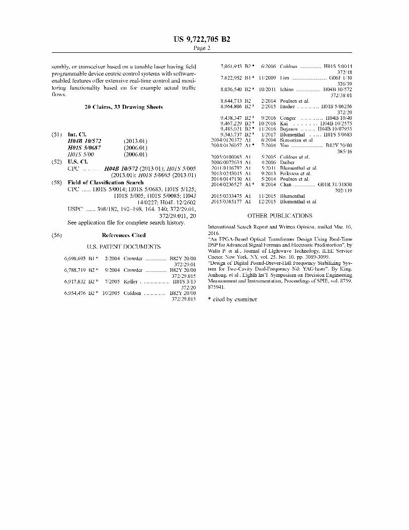
US 9,722.705 B2 Page 2
sembly, or transceiver based on a tunable laser having field programmable device centric control systems with Software enabled features offer extensive real-time control and moni toring functionality based on for example actual traffic flows.
20 Claims, 33 Drawing Sheets
(51) Int. Cl. H04B I/572 (2013.01) HOIS 5/0687 (2006.01) HOIS 5/OO (2006.01)
(52) U.S. Cl. CPC ............ H04B 10/572 (2013.01); HOIS 5/005
(2013.01); HOIS 5/0085 (2013.01) (58) Field of Classification Search
CPC ...... H01S 5/0014; H01S 5/0683; H01S 5/125; H01S 5/005; H01S 5/0085; H04J
14/0227; H04L 12/2602 USPC ...... 398/182, 192–198, 164, 140; 372/29.01,
372/29.011, 20 See application file for complete search history.
(56) References Cited
U.S. PATENT DOCUMENTS
6,690,693 B1* 2/2004 Crowder ................ B82Y 20/OO 372,29.01
6,788,719 B2 * 9/2004 Crowder ................ B82Y 20/OO 372,29,015
6,917,632 B2 * 7/2005 Koller ....................... HOS 3.13 372/2O
6,954,476 B2 * 10/2005 Coldren ................. B82Y 20/OO 372,29,015
7,061,943 B2 * 6/2006 Coldren ................ HO1S 5/OO14 372/18
7.622,952 B1 * 1 1/2009 Lim .......................... G06F 1/10 326/39
8,036,540 B2 * 10/2011 Ichino .................. HO4B 10,572 372/38.01
8,644,713 B2 2/2014 Poulsen et al. 8,964,806 B2 * 2/2015 Ensher ................ HOS 5.06256
372/2O 9,438,347 B2 * 9/2016 Conger .................. HO4B 10/40 9,467,229 B2 * 10/2016 Kai ......... HO4B 10,2575 9.485,021 B2 * 1 1/2016 Bujanos ........... HO4B 1O?O7955 9,543,737 B2* 1/2017 Blumenthal .......... HOS 5.0683
2004/O120372 A1 6/2004 Simsarian et al. 2004/O126057 A1* 7, 2004 Yoo ........................ B82Y 2000
385, 16 2005, 0100.065 A1 2006, OO72634 A1 2011/O116792 A1 2013,0243015 A1 2014/O1471.30 A1 2014/0236527 A1*
5/2005 Coldren et al. 4/2006 Daiber 5, 2011 Blumenthal et al. 9/2013 Eriksson et al. 5, 2014 Poulsen et al. 8/2014 Chan ................ GO1R 31,31830
TO2,119 2015,0333475 A1 2015,0365177 A1
11/2015 Blumenthal 12/2015 Blumenthal et al.
OTHER PUBLICATIONS
International Search Report and Written Opinion, mailed Mar. 16. 2016. “An FPGA-Based Optical Transformer Design Using Real-Time DSP for Advanced Signal Formats and Electronic Predistortion', by Watts P. et al., Journal of Llghtwave Technology, IEEE Service Cneter, New York, NY. vol. 25, No. 10, pp. 3089-3099. “Design of Digital Pound-Drever-Hall Frequency Stabilizing Sys tem for Two-Cavity Dual-Frequency Nd:YAG:laser'. By King, Junhong, et al.. Eighth Intl. Symposium on Precision Engineering Measurement and Instrumentation, Proceedings of SPIE, vol. 8759, 875941.
* cited by examiner

US 9,722,705 B2 Sheet 1 of 33 Aug. 1, 2017 U.S. Patent
{{}{}

US 9,722,705 B2 Sheet 4 of 33 Aug. 1, 2017 U.S. Patent
|Ou?u00 WAT HOd ppe
© **) No.. 1
U.S. Patent Aug. 1, 2017 Sheet 5 Of 33 US 9,722,705 B2
s s
† “OICH
US 9,722,705 B2 Sheet 6 of 33
######
Aug. 1, 2017 U.S. Patent

722,705 B2
/89
U.S. Patent

&###3$ $ 3,334}}
US 9,722,705 B2 U.S. Patent

U.S. Patent Aug. 1, 2017 Sheet 9 Of 33 US 9,722,705 B2
::
:
S
x: S S x E
S
s: & : & 8 & 8 : ; ; ;
(O9 (?INH
8 : 8 8 8 8 8 8 8 8 8 8 8 8 8 8 8 8 8 8 8 8 8 8 8 8 8 8 8 8 8 8 8 8 8 8 8 8 8 8 8 8 8 8 8 8 8 8 8 8 8 8 8 8 :
US 9,722,705 B2 Sheet 10 of 33
:::::
:
riod edities
8:
Aug. 1, 2017
3. * 3.
3×3×3×3.
U.S. Patent

US 9,722,705 B2 Sheet 11 of 33 Aug. 1, 2017 U.S. Patent
?sit?s szöä*********öö - Å” }}$ $ 3x3x3;{&
fittiei.

US 9,722,705 B2
?äöižºv, žš?&#öºžë?ïöö aeg- - - - - - - - - - - - - - - - - - - - - - - - - -!,|- - - - - - - - - - - -: ~~~~);- - - - - - - - - - - - - - - - - - - - - - - - - - -|- - - - - - - - - - - - - - - - - - - - - - - - - - - -|- - - - - - - - - - - - - - - - - - - - - - - - - - - -|{}
? perºxxxx+x3?xxx + 3×3×3× …” ;; .. *****?}?}; :| ...……**|z ?ºwa?, i?}?};
|****§§ x.zºº, ,xg89g%*****?×g××3×3:::::&…,|-> ~ ~ ~ ~ ~ ~ ~ ~ ~ ~ ~ ~ ~ ~ ~ ~ ~ ~ ~ ~ ~ ~ ~ ~ ~ ~ ~|||-> ~ ~ ~ ~ ~ ~ ~ ~ ~ ~ ~ ~ ~ ~ ~ ~ ~ ~ ~ ~ ~ ~ ~ ~ ~ ~ ~||§ §
Sheet 12 of 33
vujei in
Aug. 1, 2017
|- - - - - - - - - - - - - - - - - - - - - - - - - - - -|- - - - - - - - - - - - - - - - - - - - - - - - - - -|- - - - - - - - - - - - - - - - - - - - - - - -tºdo?a?y:- - - - - -,|- - - - - - - - - - - - - - - - - - - - - - - - - - - -,- - - - - - - - - - - - - - - - - - - - - - - - - - -|- - - - - - - - - - - - - - - - - - - - - - - - - - - -|- - - - - - - - - - - - - - - - - - - - - - - - - - - -|{}?z
U.S. Patent

US 9,722,705 B2 Sheet 13 of 33 Aug. 1, 2017 U.S. Patent
V8 ‘91).
US 9,722,705 B2 Sheet 14 of 33 Aug. 1, 2017 U.S. Patent

722,705 B2 9 US 9 Sheet 15 Of 33 1, 2017
W6 (?INH
Aug U.S. Patent

US 9,722,705 B2
No. :::::::::::::::::::::::::::::::::::::
Sheet 16 of 33 Aug. 1, 2017 U.S. Patent

US 9,722,705 B2 Sheet 17 Of 33 Aug. 1, 2017 U.S. Patent
VOI ‘OIMH
z x,x :
705 B2 9 US 9,722 Sheet 18 of 33 , 2017 1. Aug U.S. Patent
‘OIMH


::::::::::::::::::
US 9,722,705 B2 Sheet 20 of 33 Aug. 1, 2017
r
-No. £{{:::::::::::::::::::::::::::::::::::::::: U.S. Patent
US 9,722,705 B2 Sheet 21 of 33 Aug. 1, 2017 U.S. Patent
/ IZT
© I **) | H |
TOZT assssssssssssssssssssssssssssssssssssssssssssssssssssssssssssssssssssssssssssss
US 9,722,705 B2 Sheet 22 of 33 Aug. 1, 2017 U.S. Patent
Y s-wa. -- a- - - - - - -- - - - a wa- - - a -- wa, - a. a- - - - - -
383 §3 x 3. §§§3.
ezet
4: I º ‘DI ( 1

US 9,722,705 B2 Sheet 23 of 33 Aug. 1, 2017 U.S. Patent

US 9,722,705 B2 Sheet 24 of 33 Aug. 1, 2017 U.S. Patent
uol?onpaae u?punwau'r I?eH uænado
punc

US 9,722,705 B2 Sheet 25 Of 33 Aug. 1, 2017 U.S. Patent
9 LI **) No.. !

US 9,722,705 B2 Sheet 26 of 33 Aug. 1, 2017 U.S. Patent
ainoa??olvasqve,

US 9,722,705 B2 Sheet 27 Of 33 Aug. 1, 2017 U.S. Patent
WSO/WSO.
SOWO "SOW Ben-G poA end 33.
uoinci3SiO pue Bugouen beS O-3 uo pue O3 uOA
U.S. Patent Aug. 1, 2017 Sheet 28 of 33 US 9,722,705 B2
x:
{{:388

722,705 B2 9 US 9 Sheet 29 Of 33 , 2017 1. Aug U.S. Patent
890? |- 990 Z
690€.
| 24 **') ) {
US 9,722,705 B2 U.S. Patent
US 9,722,705 B2 Sheet 31 of 33 Aug. 1, 2017 U.S. Patent
© **) No.!

US 9,722,705 B2 Sheet 32 of 33 Aug. 1, 2017 U.S. Patent
V8, **) No.! ----------------'-----------------
U.S. Patent Aug. 1, 2017 Sheet 33 Of 33 US 9,722,705 B2
.
*
...s. ::
&
*** as:
s - &
. --- s
sa

US 9,722,705 B2 1.
METHOD AND APPARATUS FOR CONTROLLING, MONITORING, AND COMMUNICATING WITH TUNABLE
OPTICAL DEVICES AND SUBASSEMBLES
CLAIM OF PRIORITY UNDER 35 U.S.C. S 119
This patent application claims benefit of U.S. Provisional Patent Application Ser. No. 62/082.545 filed on Nov. 20, 2014, titled “Methods and Apparatus for Controlling Tun able Optical Devices and Subassemblies, the entire disclo sure of which is incorporated herein by reference in its entirety.
10
BACKGROUND 15
Today’s fiber optic based networks use transceivers as the interface between electronics and optical signals that propa gate on the optical fiber and at other points in the network where information is converted between electronic form and optical form. 2O
Optical devices, including optical, photonic and optoelec tronic devices and components are used to transmit, code, receive, and decode optical data for transmission on an optical fiber. The optical devices are interfaced to a variety of electronic circuits which are used to control the devices as and components, as well as interface data in electronic form on the transmit and receive side, code and decode electronic data, perform other functions like clock recovery and error correction and realize functions required to control an envi ronment of the circuitry including temperature, wavelength and other tunable laser functions and functions of the interface optics and circuits that are used to realize a fully operational tunable laser and tunable Subassembly.
Programmable optical devices, such as transmitters, opti cal Subassemblies, and transceivers, based on a tunable laser, require many control systems to Support the functions of the 35 tunable laser and Support the control, monitoring and com munications functionality. A widely tunable laser includes multiple sections, generally including a gain section, a tunable phase section, and tunable mirror sections and in Some designs a tunable filter section is also incorporated. 40 Tuning the physical parameters of these sections results in tuning of an output laser wavelength. Other parameters of the tunable laser include an optical data modulator, if it is integrated or not integrated, and other functions like power control, wavelength locking, linewidth narrowing and con trol, modulation control, higher order modulation, or the like, performance of which may be enhanced using the present disclosure.
Examples of prior art references may include “Control of Widely Tunable SSG-DBR Lasers for Dense Wavelength Division Multiplexing.” Journal of Lightwave Technology, vol. 18, No. 8, August 2000; U.S. Pat. Nos. 6,954,476: 6,788,719; 6,690,693; and U.S. Pat. App. No. 2004/ 0120372, the entire disclosures of which are incorporated herein by reference in their entirety. Known prior art programmable wavelength tunable trans- 55
mitters, such as transmitter optical Subsystem assembly (TOSA), transceivers and other communications optical Subassemblies, however, are not programmable in real-time and thus lack flexibility and responsiveness at the optical layer. Further, as the existing devices lack real time pro- 60 grammability, there is a high cost associated with planning, building, operating and maintaining data center networks.
30
45
50
SUMMARY 65
It is to be understood that both the foregoing general description and the following detailed description are exem
2 plary, and are intended to provide further explanation of the present technology or disclosure as described. The present disclosure relates generally to optical devices
and Subassemblies, such as optical transceivers, modules and Subassemblies as well as laser transmitters and receivers that employ integrated electronics and photonic integrated circuits and combinations thereof. The optical devices and Subassemblies contain multiple elements, for example, widely tunable semiconductor lasers integrated on the same Substrate with optical modulators and semiconductor optical amplifiers, non-integrated optical and optoelectronic ele ments, and other measurement and control devices and elements.
In an aspect, an apparatus for controlling, monitoring, and communicating with an optical device, photonic integrated circuit or Subassembly for optical communications is pro vided. The apparatus includes an optical device or Subas sembly and a field programmable device including program mable hardware gates coupled to the optical device or Subassembly. The field programmable device is configured to implement a plurality of functions at a gate level for controlling, monitoring, and/or communicating with the optical device or subassembly, each of the plurality of functions being configured to execute as a concurrent pro cess, without use of a microprocessor or a microcontroller.
In an aspect of the present disclosure, an optical commu nication system includes an optical device or Subassembly comprising a tunable laser integrated on a same Substrate with an optical modulator and a semiconductor optical amplifier, non-integrated optical and optoelectronic ele ments; and a field programmable device including program mable hardware gates coupled to the optical device or subassembly and the laser transmitter and receiver. The field programmable device is configured to implement a plurality of functions at a gate level for controlling, monitoring, and/or communicating with the optical device or Subassem bly, each of the plurality of functions being configured to run as a concurrent process, without use of a microprocessor or a microcontroller. The field programmable device of the optical communication system comprises one or more field programmable gate arrays (FPGAs) or programmable logic devices (PLDs). Further, the field programmable device of the optical communication system may be configured to comprise application programmable interfaces (APIs) for real-time control and monitoring of the optical device and subassembly based on actual traffic flows. Also, the plurality of functions may be configured to run at different clock signals in the field programmable device. Further, the field programmable device may comprise a communication inter face including one or both of sockets to a graphical user interface (GUI) or an application programming interface (API) that allows control, monitoring and/or communication with the tunable laser integrated on the same substrate with the optical modulator and the semiconductor optical ampli fier, non-integrated optical and optoelectronic elements.
In another aspect, the present disclosure comprises real time programmable optical devices and Subassemblies. Such as wavelength tunable transmitters (e.g., TOSA), transceiv ers, and other communications optical Subassemblies. According to the present disclosure, Software-enabled fea tures, accessible via application programmable interfaces (APIs), offer extensive real-time control and monitoring of the optical devices and subassemblies based on, for example, actual traffic flows. Programmability enables an unprecedented level of flexibility and responsiveness at the optical layer with real-time scaling and rerouting of band width, higher bandwidth extraction from a given fiber plant

US 9,722,705 B2 3
as well as a reduction in complexity and related cost of planning, building, operating and maintaining data center networks.
In an aspect of the present disclosure, programmable systems, methods and devices are provided to control, monitor and communicate with tunable lasers, tunable trans mitters, tunable transceiver pluggables and Subassemblies, and board mounted tunable transceivers and the auxiliary integrated or non-integrated optics, optoelectronics and/or electronics. The systems, methods and devices described herein realize functions to design, build, produce and manu facture a fully functional tunable laser, tunable transmitter, tunable transceiver, pluggable, Subassembly or board mount. The present disclosure implements monitoring and control and communications functions for the tunable laser, trans ceiver, module or optical Subassembly in a field program mable device including a field programmable gate array (FPGA) or programmable logic device (PLD) circuitry architecture, or in combination with a microprocessor or microcontroller.
Both the FPGA and PLD circuitry are reconfigurable circuitry, which can be programmed/re-programmed in the field and/or real-time after manufacture. According to the present disclosure, the control functions of the optical device or Subassembly can be implemented without a microcon troller or microprocessor. For example, various functions including control functions may be embedded in the FPGA or PLD. By way of example, the functions that are embed ded in the FPGA or PLD include, but are not limited to, soft state machines, electronic filters, control and feedback loops, decisions circuits, communications interfaces, etc., which are implemented by embedding concurrent processes in the FPGA, the PLD or the combination of programmable logic and microprocessor. The present disclosure is an advance over existing technologies that utilize microproces sors or microcontrollers for control and programmable logic devices such as FPGAs or PLDs to store calibration and other data for lookup operation(s).
Other advantages of the present disclosure are described in further detail below. By way of example, the control, monitoring and communications functions to build and operate a tunable transmitter, tunable laser, tunable trans ceiver, pluggable or Subassembly may be programmed in hardware gates in the FPGA, using firmware, each running at their own clock speed and implemented modularly. The concurrency, modularity, ability to run processes at different clock speeds, may result in advances over the existing technology for reduced costs, complexity, power consump tion, and other advantages.
The present disclosure includes, but is not limited to, the control, monitor and communications method and apparatus for a tunable laser/transceiver which is programmable and firmware updatable, and may be fully FPGA controlled (no microprocessor or microcontroller required). Embodiments of the present disclosure may include, but are not limited to:
Communications interfaces to/from a client or host or fiber communications channel;
Tunable laser wavelength memory and management; Programmable read only memory (PROM)-serial periph
eral interface (SPI) FLASH interface to external eras able programmable read-only memory (EPROM);
Set currents and Voltages for all control and monitoring functions for the tunable laser, modulator, optoelectron ics, electronics, sensors and other control and monitor points that interface via Voltages and currents;
Optical and electronic and photonic integrated circuit (PIC) monitors;
10
15
25
30
35
40
45
50
55
60
65
4 Boxcar averagers and other signal processing functions; Automatic optical power control; Wavelength locking: Linewidth narrowing algorithms and circuits (e.g., Pound
Dreyer Hall (PDH)); Temperature monitoring and control; Alarm and monitoring control and communications; Application programmable interfaces (APIs); and Fully calibrated Stand-alone, ready for integration into
pluggables or on-board—digital control/monitoring/ data onboard calibrated EPROM.
According to an aspect of the present disclosure, control systems and methods are provided to rapidly control an optical device and/or Subassembly. The control systems and methods comprise functionality to control elements of the optical device or Subassembly, such as a tunable laser, internal and external optical and optoelectronic monitoring and control functions, internal and external electronic moni toring and control functions, signal processing functions, and associated functions in a transceiver, optical module and/or optical Subassembly.
According to another aspect of the present disclosure is an implementation of the embodiments of the control systems and methods according to the present disclosure in a field programmable device, such as a FPGA, PLD, or the like, either stand alone or in combination with a microcontroller, and/or in combination with analog to digital converting (ADC) and digital to analog converting (DAC) circuits, where the FPGA, PLD, or the like is used for the control functions as part of the first embodiment, beyond the simple present day use of FPGAs and PLDs as data storage only mechanisms, for example, lookup tables fortunable lasers. This embodiment of the present disclosure thus provides various advantageous over the existing technology, which utilizes FPGAs and/or PLDs in a limited capacity to store data about tunable lasers and other embodiments to be accessed by other processing modules for monitoring, con trol and processing, but not for the control systems and methods as described herein.
In an aspect of the present disclosure, the field program mable device may be configured to automatically adapt laser control currents of a tunable laser to measured temperature so as to reduce a load on a thermoelectric cooler (TEC), based on the measured temperature and at least one of by moving between tables stored in the field programmable device or by extrapolating between temperature wavelength maps. An advantage of using the field programmable device,
such as the FPGA, PLD, or the like, as part of the control systems and methods according to the present disclosure is that code and processes may be modular and/or concurrent processes, each may run at different, unique clocks speeds within the same device and is reprogrammable, and can handle all control, monitoring, and communication embodi ments. Accordingly, in an aspect of the present disclosure, one or more submodules of the system can be replaced, modified, programmed, and/or re-programmed without affecting other modules/submodules. As such, advantages of running the control, monitoring, and communications sys tems of the optical devices and Subassemblies in a program mable manner at a gate level may include lower power consumption, lower cost, wider use across broader classes of applications, and introduction of new control modules of a variety of types (filter, analog circuits, state machines, etc.) in a common programmable architecture.
According to another of the present disclosure, the meth ods and systems described herein may be utilized with a

US 9,722,705 B2 5
multi-facet laser architecture, as described in U.S. patent application Ser. No. 147146,717, published on Jul. 10, 2014 as WO2014/107537, which is incorporated herein by refer ence in its entirety. As described in WO2014/107537, two or more facet of a tunable laser may be used for an output and may be connected to a novel modulator structure. The control and monitoring described in the present disclosure, in certain forms, may have additional advantages over prior state of the art when combined with the inventions described in WO2O14/107537.
According to an aspect, the present disclosure may be employed with optical devices and Subassemblies that use an FPGA centric architecture. Examples of devices and subas semblies may include U.S. Pat. No. 8,644.713, and U.S. patent application Ser. No. 14/171.480, titled “Program mable Optical Subassemblies and Modules'; Ser. No. 12/945,470, titled “Optical Network Interface Module Using A Hardware Programmable Optical Network'; and Ser. No. 13/942,519, titled “Control Systems for Optical Devices and Subassemblies,” which are incorporated herein by reference in their entirety. The FPGA centric architecture may run all control, monitoring, communications, algorithms using an internal FPGA without use of a microprocessor or micro controller in these optical devices and Subassemblies.
According to the present disclosure, the same firmware for an external FPGA may also be used to calibrate the laser and significantly speed up the calibration speed, where the resulting calibration data is then ported to a wavelength control FPGA which is used to control the tunable laser, making the calibration during manufacturing and the control and re-calibration or re-programming uniform with FPGA technology and firmware across all embodiments of the use of a tunable laser from manufacturing to deployment in a network. As such, the present technology may significantly cut down on the cost of manufacturing and ownership as well as improving performance.
According to another aspect of the present disclosure, a communications interface may be integrated into the field programmable device (e.g., FPGA) as described in U.S. patent application Ser. No. 12/945,470, which is incorpo rated herein by reference in its entirety, as well as associated patents and patent applications. The communications inter face may comprise sockets to graphical users interfaces (GUIs) and/or application programmable interfaces (API) that allow software control, monitoring and calibration of a complete tunable laser using a Software layer that interacts with the tunable laser through the field programmable device (e.g. FPGA or PLD or the like) to implement one of any of the fast wavelength calibration algorithms, making the ease of use, manufacturability, speed of calibration, and integra tion into other manufacturing, system integration and net work operation systems enabled and significantly lower cost and flexible compared to any existing approach. The speed of the calibration routines, on the order of minutes, may even allow recalibration in the field or real-time using the appli cation layer interfaces via the field programmable device (e.g., FPGA, PLD or the like).
In another aspect of the present disclosure, the field programmable device may be configured to receive one or more control signals from a GUI coupled to the field programmable device via wireless communications or from a GUI of another apparatus located at a remote site over an optical communication link.
Other significant advantages of the present disclosure may also include the ability to utilize processes embedded in the field programmable device (e.g., FPGA, PLD or the like), in addition to control and monitoring interfaces, to realize all
10
15
25
30
35
40
45
50
55
60
65
6 functions needed to improve the performance of the tunable laser and transmitter using firmware, for example, narrowing a laser linewidth for coherent communications, reducing the laser relative intensity noise (RIN), as two of many examples. These processes may be run in parallel with all other processes for the tunable laser, transmitter, transceiver, module or Subassembly, and in many cases can re-use hardware used for other functions.
BRIEF DESCRIPTION OF THE DRAWINGS
A more detailed understanding may be obtained from the following description in conjunction with the accompanying drawings.
FIG. 1A illustrates a block diagram conceptually showing components for a field programmable device centric control system in accordance with an aspect of the present disclo SUC.
FIG. 1B illustrates an example of a field programmable device in accordance with an aspect of the present disclo SUC.
FIG. 1C illustrates an example of how functions are implemented as concurrent, independent processes in the field programmable device.
FIG. 2 illustrates a typical implementation of a tunable laser or transceiver control, monitor, and communications using a microprocessor or microcontroller based architec ture.
FIG. 3 illustrates an example of an implementation of a Register Write operation in accordance with an aspect of the present disclosure.
FIG. 4 illustrates an example of a block diagram of a photonic integrated circuit (PIC) tunable modulator.
FIG. 5 is an example block diagram of an external control function or loop using the field programmable device tech nology in accordance with an aspect of the present disclo SUC.
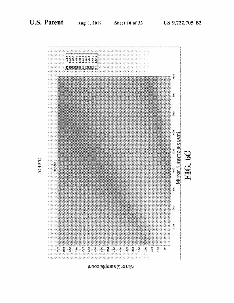
FIGS. 6A-6C illustrate examples of gain voltage maps obtained by tuning laser mirror currents of a tunable laser at three different temperatures in accordance with an aspect of the present disclosure.
FIGS. 7A and 7B are examples of tuning approximations for two laser mirror currents at 1542.02 nm and 1577.16 mm wavelengths versus temperature.
FIGS. 8A-11B illustrate examples of graphical user inter faces (GUIs) that are configured to communicate through processes running in a field programmable device.
FIG. 12 illustrates a typical implementation of an analog PDH control system.
FIG. 13 illustrates an example implementation of a PDH feedback loop in accordance with an aspect of the present disclosure.
FIG. 14 illustrates an example implementation of a PDH algorithm in accordance with an aspect of the present disclosure.
FIG. 15 illustrates an example implementation of the PDH algorithm in accordance with an aspect of the present disclosure.
FIG. 16 shows an example of an equation for detected power from an etalon reflected optical signal in accordance with an aspect of the present disclosure.
FIG. 17 illustrates an example implementation of the PDH algorithm in accordance with an aspect of the present disclosure.
FIG. 18 illustrates an example block diagram of firmware control of a field programmable device and other devices in accordance with an aspect of the present disclosure.
US 9,722,705 B2 7
FIG. 19 illustrates an example of general etalon reflected and transmitted responses in accordance with an aspect of the present disclosure.
FIG. 20 illustrates an example of a block diagram illus trating an example implementation of a wavelength locking algorithm, in accordance with an aspect of the present disclosure.
FIG. 21 illustrates an example diagram of one implemen tation of a temperature control process in accordance with an aspect of the present disclosure.
FIG. 22 illustrates a block diagram of a symbolic model of one channel of the boxcar filter in accordance with an aspect of the present disclosure.
FIG. 23A illustrates an example address spacing of a flash memory in accordance with an aspect of the present disclo SUC.
FIG. 23B illustrates an example of a wavelength defini tion table in accordance with an aspect of the present disclosure.
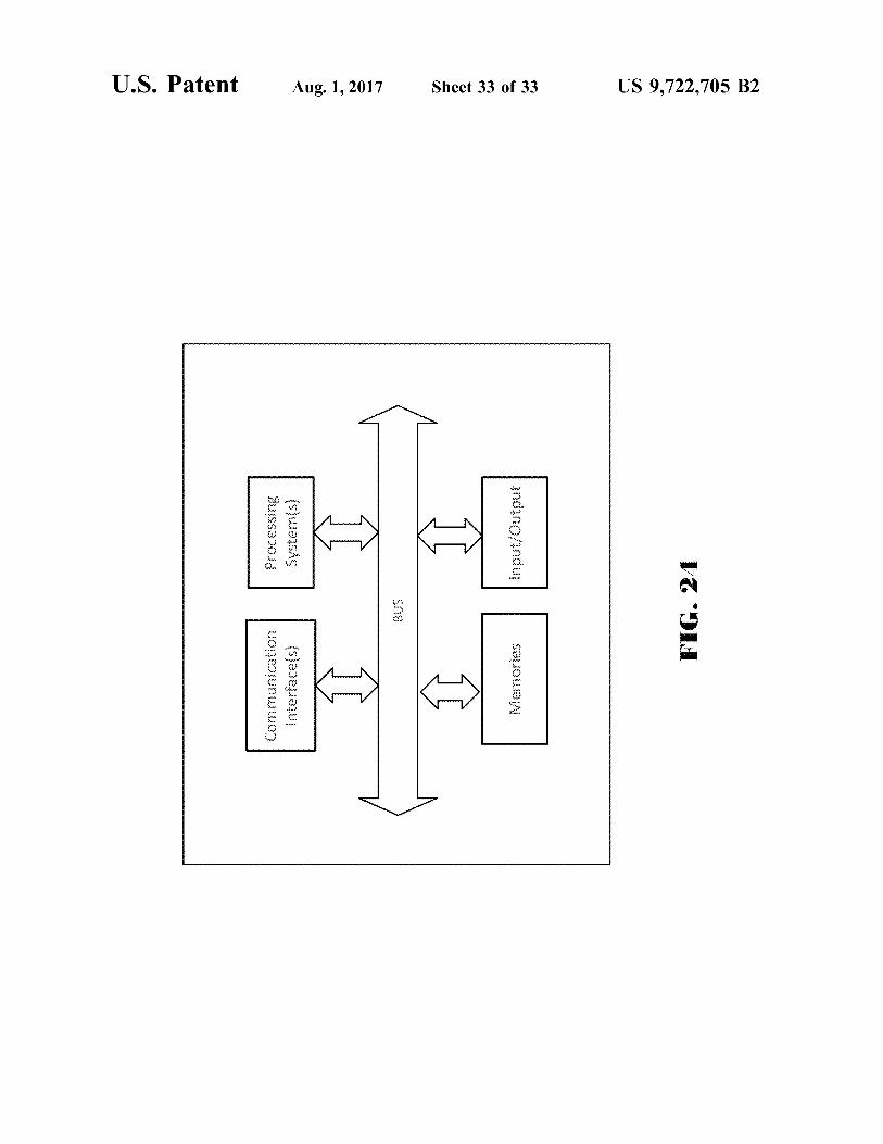
FIG. 24 illustrates an example of an implementation of one or more processing systems in accordance with an aspect of the present disclosure.
DETAILED DESCRIPTION
According to the present disclosure, optical devices, such as optical transmitters, optical Subassemblies, and transceiv ers which are programmable are described. By way of example, the programmable optical devices are based on a tunable laser having field programmable device centric (e.g., a FPGA or a PLD centric) control systems which support various functions of the tunable laser and supporting control, monitoring and communications functionality. The present disclosure comprises real-time programmable wavelength tunable transmitters, such as transmitter optical Subassem blies (TOSAs), transceivers, and other communications optical Subassemblies.
FIG. 1A illustrates a block diagram conceptually showing components for a field programmable device centric (e.g., FPGA/PLD centric) control system. A system 100 shown in FIG. 1 includes a host controller 101, a field programmable device 103 (e.g., FPGA, PLD or the like), laser control electronics 105, a tunable laser 109, and a storage 111. The host controller 101 may be configured to communicate with the field programmable device 103 for various functions, and also configured to receive data relating to operation of the tunable laser 109. In the example, the field program mable device 103 may drive the laser control electrodes 105 through digital-to-analog converters (DACs) 107 interfaced to the field programmable device 103 and the tunable laser 109. Further, the field programmable device 103 may be coupled to the tunable laser 109 through analog-to-digital converters (ADCs) 117 for communications and control of the tunable laser 109.
Further, the field programmable device 103 may also include various components, modules or processes (which are not shown in FIG. 1A, but described herein in detail), Such as communication interfaces to/from a client or host for fiber communications channel; tunable laser wavelength memory and management; PROM-SPI Flash interface to external memory; setting currents and Voltages for all con trol and monitoring functions for the tunable laser, modu lator, optoelectronics, sensor and other control and monitor points that interface via Voltages and currents; optical and electronic and photonic integrated circuit (PIC) monitors; boxcar averagers and signal processing functions; automatic optical power control; wavelength locking; linewidth nar
10
15
25
30
35
40
45
50
55
60
65
8 rowing functions, temperature monitoring and control; alarm and monitoring control and communications; appli cation programming interfaces (APIs); and many other functions for implementing various aspects of the present methodology described herein. Further, the field program mable device 103 may include an internal storage (not shown) and/or an external storage Such as the storage or memory 111 coupled to the field programmable device 103 for storing various parameters including parameters for implementing various aspects of the present technology. In an aspect of the present disclosure, the memory 111 may include one or more look-up tables of data in connection with implementing various aspects of the present technology described herein.
Further, in an aspect of the present disclosure, a field programmable device-centric architecture (e.g., FPGA, PLD or the like centric) may be implemented as follows. The host controller 101 may transfer code for one or more algorithms, modules, processes or functions to the field programmable device 103, either as high level programming language (e.g., C code or the like) in an embedded soft processor, or for even more efficiency and high speed, as hardware descrip tion language (e.g., HDL code or the like). The host com puter 101 may also be connected through a standard inter face, i.e., a universal serial bus (USB) connection, to the field programmable device 103. As noted, while performing various aspects of the present technology, the field program mable device 103 may communicate directly with DACs 117 that are configured to drive currents to various compo nents including laser mirrors of the tunable laser 109 and communicates with ADCs 107 that are configured to moni tor the electrode voltages and/or power detectors to collect data from the tunable laser 109 in accordance with various aspects of the present technology. Alternatively, and/or in addition to, the field programmable device 103 may control transients in laser temperature by monitoring a thermistor on the tunable laser 109 and driving a current control input to a TEC controller of the tunable laser 109. Further, the field programmable device 103 may buffer or store data relating to controlling, monitoring, and communicating with the tunable laser 109 in one or more storage devices, such as the memory 111, whether it is internal or external to the field programmable device 103, to perform various functions, methods, algorithms or methodologies, in accordance with aspects of the present disclosure.
In an aspect of the present disclosure, the present tech nology may be viewed as a field programmable device (e.g., FPGA, PLD or the like) centric architecture for optical communications systems. As such, the one or more imple mentations of the present technology may be optimized for a hardware architecture and the methodology or algorithm itself, incurring negligible overhead in the processing of various aspects of the present technology in the field pro grammable device 103, and thus data transfers to and from the coupled ADCs 107, DACs 117, and storage 111 may be very efficient.
In another aspect, the present disclosure provides Soft ware-enabled features accessible via application program mable interfaces (APIs), offering extensive real-time control and monitoring of one or more modules or processes based on, for example, actual traffic flows. Such programmability provides an unprecedented level of flexibility and respon siveness at an optical layer with real-time scaling and rerouting of a bandwidth, a higher bandwidth extraction from a given fiber plant as well as a reduction in complexity and related cost of planning, building, operating and main taining data center networks. Rapid control of all aspects of
US 9,722,705 B2
a tunable laser, in which more than one facet are optically available, or integrated transmitter photonic integrated cir cuit (PIC) assembly that combines a tunable laser and modulator, or optical transceiver or optical Subassembly is provided. That is, the present disclosure may provide control which is modular, concurrent, independent processes, fast and reprogrammable, and thus may handle all control, monitoring, and communication aspects, in which any Sub module of a system may be replaced, modified, programmed without affecting other modules or processes. In other words, in an aspect, the control, monitoring, and commu nications system may comprises modular, independent, and/ or concurrent processes configured to run in the field pro grammable device, each of which may be configured to run at different clocks. The advantage of running all control, monitoring and communications in a programmable manner at a gate level may result in lower power, lower cost, wider use across abroader classes of applications, and introduction of new control modules of a variety of types (filter, analog circuits, state machines, etc.) in a common programmable architecture. As such, the present disclosure may provide for control,
monitoring, communications, and algorithm implementa tions using an internal field programmable device Such as am FPGA, PLD, or the like, without using a microprocessor or a microcontroller, and may even use the same firmware for an external FPGA, which is used to calibrate a tunable laser, thereby significantly speeding up the calibration speed of the tunable laser. The resulting calibration data may then be ported to a wavelength control FPGA which is used to control the tunable laser, making the calibration during manufacturing and the control and re-calibration or re programming uniform with the field programmable device based technology described herein and firmware across all aspects of the use of a tunable laser from manufacturing to deployment in a network, significantly cutting down on the cost of manufacturing and ownership as well as improving performance.
In an aspect of the present disclosure, the communications interface into the field programmable device 103 may pro vide gate level general programming and interfaces for graphical users interfaces (GUIs) and/or application pro grammable interfaces (API) that allow software control, monitoring and calibration of a complete tunable laser using a software layer that interacts with the tunable laser through the field programmable device 103 to implement one of any of the algorithms described herein including the fast wave length calibration algorithms, making the ease of use, manu facturability, speed of calibration, and integration into other manufacturing, system integration and network operation systems enabled and significantly lower cost and make flexible compared to any prior existing technology. The speed of the calibration routines, on the order of minutes, may even allow recalibration in the field or real-time using the application layer interfaces via the field programmable device (e.g., FPGA, PLD or the like).
Advantages of the present disclosure may include, but not limited to, many significant advantages over the existing technology that uses a microcontroller or microprocessor as a main control and an FPGA primarily as a data storage and lookup device. In the past, the performance as a function of footprint and power consumption of field programmable devices such as FGPAs was not considered competitive to microprocessors to handle various functions required for real time data and control in tunable laser applications. However, in recent years, field programmable device tech nology, including FPGA, PLD, or the like technology, has
10
15
25
30
35
40
45
50
55
60
65
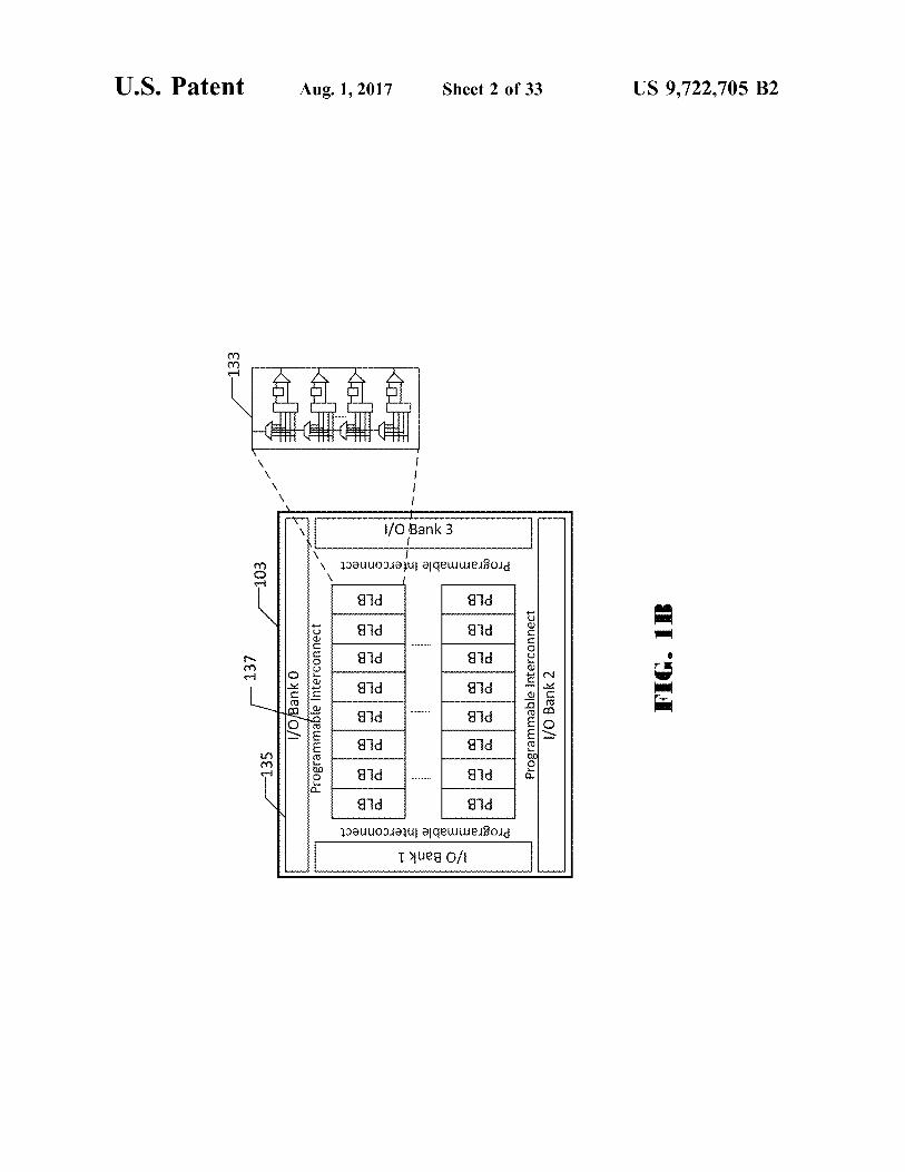
10 advanced significantly and has become a preferred and more flexible method and apparatus to control, monitor and com municate than many microcontroller or microprocessor based solutions. By way of example, as shown in FIG. 1B, a field
programmable device Such as an FPGA is an integrated circuit that can be programmed in the field or real-time after manufacture, unlike certain integrated circuits such as a microcontroller or a microprocessor, which is hard-core. That is, FPGAs are semiconductor device that are based on a programmable/configurable logic blocs connected via pro grammable interconnects or wiring circuits, thereby enabling the FPGAs to be reprogrammable to desired appli cation or functionality requirements after manufacturing. In other words, an FPGA is a device based on a gate and device interconnection loaded into the FPGA to operate on data and signals at inputs to generate outputs. In one implementation, the field programmable device 103 may include an FPGA or PLD or the like comprising a plurality of configurable logic blocks (CLBs) 133, a plurality of input/output (I/O) ports 135, programmable interconnect 137, etc. Each configurable logic block 133 (CLB) may include various components, Such as carry logic, input look-up tables, flip-flops, etc. The operation of the FPGA as well as the clock speed of different processes running on the FPGA may be changed in real time, and thus a wide variety of control, monitoring, feedback, communications and other functions may be realized with hardware level performance in the FPGA. Thus, by way of example, in accordance with an aspect of the present dis closure, a field programmable device (e.g., FPGA, PLD, or the like) based architecture may enable concurrent control, monitoring, and communications processes for the tunable laser or tunable laser based module.
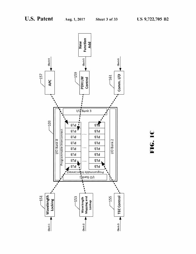
Further, as shown in FIG. 1C, different areas of the FPGA circuitry may be allocated or used to implement different data and/or control functions all within the single device. By way of example, in FIG. 1C, a plurality of data and/or control functions or modules may be implemented in one or more PLBs, e.g., a wavelength locking 151, wavelength mapping and lookup 153, TEC control 155, automatic power control (APC) 157, PHD Linewidth control 159, communi cations I/O 161, etc., each running at different clock signals, e.g., clock 1, 2, ... 6. Further, a new module or process such as a PDH linewidth (LW) control 159 with a clock signal (e.g., clock 5) may be added in real-time.
In an aspect of the present disclosure, Some functions that may be realized in accordance with various aspects of the present technology may include but are not limited to:
Control of optical properties of a data modulated tunable laser including a chirp of a transmitted optical signal and adjusting the control based on an output wave length of the tunable laser and other parameters;
Temperature monitoring and control of temperature sen sitive components (e.g., laser, etalon, etc.);
Control and/or adjustment of a laser output power (e.g., by adjusting gain sections and Voltage controlled attenuators);
Control of a laser wavelength of a tunable laser by controlling mirrors, resonators, phase sections and other wavelength tunable elements by embedding a current-wavelength control map, that can also be a function of temperature;
Control and monitoring of a wavelength locker circuit and function. The internal mapping can also be changed in real time in response to calibration and re-calibration of the tunable laser using a wavelength locker;
US 9,722,705 B2 11
Functions that require larger memory capabilities of FPGAs, like state size, as compared to microcontrollers or microprocessors;
Concurrent processes that can operate independently of each other leading to a higher performance at a given clock speed compared to serial finite state micropro cessors, with higher fault tolerance, ability to manage power by turning on and off processes individually and updating processes individually without having to rewrite and recompile the complete code;
Continual operation upon host failure (e.g., a control interface that in the case that the host fails the unit can still continue to operate);
Corrective action (e.g., if laser output power deteriorates or laser wavelength shifts the FPGA can take corrective action per locker and other mechanisms); and
Other functions that can be reprogrammed to fit different applications. One chip or a smaller Subset of electronic chips may therefore be used across a wider variety of applications and PIC, Switches, or transmitter and receiver Subassemblies driving up the Volume and lower cost and eventually power consumption and size.
As noted above, some examples of the programmable firmware functions that may be implemented in the field programmable device 103 such as the FPGA, PLD or the like, may include but not limited to (functions or examples below may be implemented alone or in combination with others):
Host communications interfaces and memory map: Wavelength memory and management; Programmable read-only memory (PROM)-serial periph
eral interface (SPI) FLASH interface to external eras able programmable read-only memory (EPROM);
Set currents and Voltages; Optical and electronic and photonic integrated circuit
(PIC) monitors; Boxcar averagers; Automatic power control; Wavelength locking: Linewidth narrowing algorithms (like Pound Dreyer Hall
(PDH)); Temperature monitoring and control; Alarm and monitoring control and communications; and Application programmable interfaces: As noted earlier, FIG. 1C illustrates an example of how
Some of the functions that may be implemented as concur rent, modular processes, while providing an advantage over the existing technology using a microcontroller and/or a serial state machine as shown in FIG. 2, which illustrates a typical implementation of a tunable laser or transceiver control, monitor, and communications using a microproces sor or microcontroller based architecture. As shown, the microprocessor or microcontroller by design executes the functions, modules or processes in a sequential manner, for example, executing the wavelength mapping and lookup 161, wavelength locking 163, APC 165, TEC control 167, and communication I/O 168. Further, if a new function such as a PDH LW control 173 is to be added (at 171), then code need to be redesigned for the microprocessor or microcon troller.
However, as noted above, in accordance with an aspect of the present disclosure, the present technology provides the field programmable device 103 (e.g., FPGA, PLD or the like) which may implement various functions, modules or processes relating to control, monitor, and communication with a tunable laser or transceiver, as concurrent, indepen
5
10
15
25
30
35
40
45
50
55
60
65
12 dent modules or processes which are configured to run at different clock signals, without use of the microprocessor or microcontroller.
Host Communication Interfaces and Memory Map
In an aspect of the present disclosure, the field program mable device 103 may include a slave controller that may implement standard serial protocols, such as an Inter-IC bus (I2C) and/or serial peripheral interface (SPI), or other pro prietary protocols. The advantage of the present technology over any microprocessor/microcontroller or system-on-chip (SoC) based system is that the slave controller of the present disclosure is not a hard-core, and thus it may easily be modified to suit host interface requirements in the field programmable device 103. By way of example, in an aspect of the present disclosure,
a register map architecture may be based on two dual port random access memories (RAMs), one for a register map and one for wavelength table data which may be imple mented in (or external but coupled to) the field program mable device 103. Host read/writes to the register map may then be directly addressed to one port of the register table RAM, while up/download of the wavelength table data is accomplished through a set of registers that include the parameters for a single wave table entry and redirect this data to an appropriate location in a wave table RAM. The second RAM port may be used for updating of digital-to analog (DAC) data from RAM, reading of analog-to-digital (ADC) monitor data to RAM, and updating of laser/modu lator control parameters from the wave table RAM when wavelength is changed or as dictated by a system. Dedicated control logic may perform RAM to ADC/DAC transactions, without the use of a microcontroller or microprocessor. The logic implemented in the field programmable device 103 may be optimized further for transfer efficiency, has pre dictable latency, and can be tuned to prioritize transactions that require very low latency.
In another aspect of the present disclosure, a registered memory map of the field programmable device 103 may be implemented within the field programmable device 103 and controlled via a host communication interface. The regis tered memory map may define a current state of a control system, which in turn determines the wavelength and output power of a tunable laser assembly. The state of a control system may be a result of electrode currents, bias Voltages, device operating temperature and various configurable set tings associated with the tunable laser like a TEC PID control loop and wavelength locker, for example. All of these individually configurable modules or processes may be changed and monitored by writing to or reading from an appropriate register in the registered memory map of the field programmable device 103, without the use of the microprocessor or microcontroller. By way of example, an example implementation of a
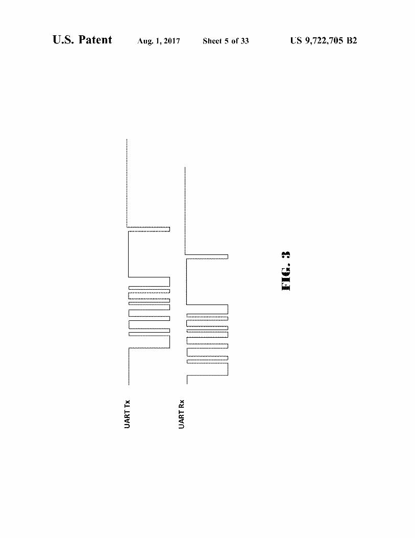
Register Write operation via UART is shown in FIG. 3. In the implementation, a UART is used to communicate to an I2C device. As shown in FIG. 3, the field programmable device 103 receives a command from a host or host con troller 101 via a UART string (e.g., UART Tx from the host to the field programmable device), the UART string is echoed back to the host or host controller (e.g., UART RX from the field programmable device to the host), the com mand is then interpreted, and an I2C command is issued to a register interface on the I2C bus coupled to the field programmable device 103. The UART then sends a string

US 9,722,705 B2 13
back with the written data. In the implementation, for a register write cycle it may take approximately 1.2 ms.
Automatic Power Control (APC)
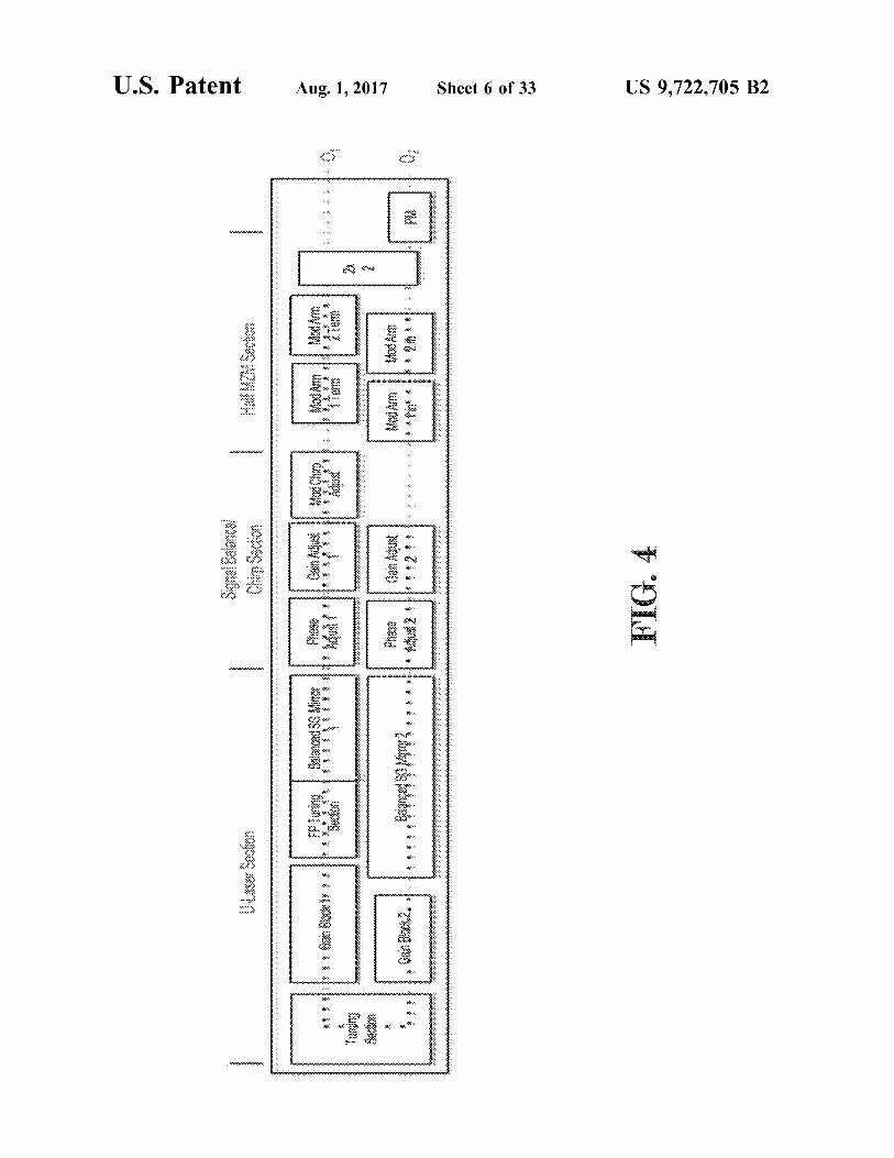
In an aspect of the present disclosure, an automatic power control (APC) function or loop may be implemented as a concurrent, independent module or process within the field programmable device 103. An APC control function or loop dynamically maintains a laser output power at a commanded level while also maintaining a ratio of semiconductor optical amplifier (SOA) currents in a tunable laser (e.g., a U-Laser), which in turn maintains a balance of photocurrents in Mach Zehnder modulator legs, which is required for proper modu lation. FIG. 4 illustrates a block diagram of an example PIC tunable modulator as described in U.S. Patent Application Ser. No. 61/748,415, published on Jul. 10, 2014 as WO2014/ 107537 with elements that enable APC and the APC loop. Further, an example block diagram of an external control function or loop using the field programmable device tech nology such as FPGA, PLD or like technology is also shown in FIG. 5.
In an aspect of the present disclosure, a field program mable device 531 (similar to the field programmable device 103 shown in FIG. 1A) may include an averaging filter 533, a SOA balancing 535, a loop filter 537, and a DAC control 539. In the example, the averaging filter 533, SOA balancing 535, loop filter 537, and DAC control 539 may all be implemented digitally as one or more concurrent, indepen dent modules or processes within the field programmable device 531. The field programmable device 531 (e.g., FPGA or PLD or the like technology) is configured to allow performing these functions optimally and with low fixed latency and high noise immunity. Further, in the example, current DAC 551 and ADC 559 may be located outside but coupled to the field programmable device 531, and the field programmable device 531 drives the laser SOA currents to a tunable laser (e.g., U-laser 553) through the external current DAC (e.g., Current DAC 551). The detected optical powers, via detectors 557, from two legs of the Mach Zehnder Modulator 555 may be digitized in the external ADC 559 and input to the field programmable device 531, which first passes them through the averaging filter 533 to Smooth a response and filter noise picked up in an analog path. The filtered detected powers are input to the SOA bal
ancing 535, which starts with default SOA currents provided from a wavelength table (not shown) and then measures the detected powers to determine a proper ratio of SOA currents to maintain balanced MZM outputs. This ratio is fed to the loop filter 537 along with TX Power, which is the power out of leg 1 of the Mach-Zehnder Modulator 555, and total power, which is a sum of the powers in the two modulator legs. The linear loop filter 537 may be configured to adjust SOA1 and SOA2 currents in fixed steps, while maintaining a ratio of the SOA1 to SOA2 currents until a desired Tx power is attained. An initial step size in the larger of SOA1 or SOA2 may be in 1000 uA increments. When the output power is within one 1000 uA increment, the step size may be reduced to 125 uA and a final “Vernier search may be performed until the output power is within one 125 uA step. If the measured power changes by more than 2 counts or 250 uA, the Vernier search resumes. If the tunable laser is reinitialized (e.g., turned off and then on), however, a crude search may restart followed by the Vernier search.
It is also noted that theoretically, SOA current may affect laser wavelength tuning and stability through its electrical
5
10
15
25
30
35
40
45
50
55
60
65
14 and thermal effects. When SOA current changes, its control circuits could affect the circuits that control the laser's gain sections, laser phase section and mirror sections, thus affect the wavelengths tuning and stability. In addition, SOA current change could affect the thermal stability around the mirrors, which affects the mirrors performance, in turn it affects the wavelength tuning and stability.
In one implementation of the APC function in the field programmable device 531, the SOA power may be adjusted proportionally per wavelength using a real time control loop to maintain output power. Measurements to date have shown that, with the APC and wavelength locker modules operating cooperatively, small incremental adjustments of the SOA may not significantly affect the wavelength.
In an aspect of the present disclosure, the wavelength and power stability may be Summarized as examples as below.
State Power Wavelength Time Comments
Off <=-30 dBm +f-0.9 mm Power-on <=1 mW/s, +f-0.2 nm <30s APC may be
<=1 dB modified to Ower- reduce power shoot per specified
slope Active +f-1 dB +/-25 pm Wave
length tuning 2s
Power-off -2.1 dB +f-0.3 nm Lambda inside mask with indicated vertices as power slopes down
Power-off -5.6 dB +f-0.4 nm Power-off -7.6 dB +f-0.7 mm Off <=-30 dBm +f-0.9 mm <=2 ms Time from full
(DWDM), power to off 10 us
(SFP+)
Automatic Wavelength Mapping (AWM)
One of the limiting factors in reducing power consump tion of optical laser modules is the need for active tempera ture stabilization of a laser to keep the lasing wavelength within the specified accuracy. Typically, a laser needs to be stabilized to within +0.05°C., and especially in the extreme regions of a temperature range (a typical temperature range is -5° C. to 70° C.) the thermoelectric cooler (TEC) con figured to facilitate temperature Stabilization may consume a significant amount of power to meet this specification. For example, when the laser needs to be at a temperature of 20° C. and the environment is at 70° C., meaning that the laser package is at 80° C. to 85°C., the TEC needs to span a temperature gap of 60° C. to 65° C.
In an aspect of the present disclosure, a means to reduce a load of the TEC and in some instances completely remove the load may be provided by, instead of keeping laser control currents fixed and stabilizing the laser, letting the laser control currents automatically adapt to the temperature. To exemplify the embodiment further, instead of operating the laser at 20°C., one could operate the laser at 60°C. and thus reduce the gap from the laser temperature to the laser package temperature to 20° C. to 25°C. This may be done "dynamically, based on the measured temperature, and by moving between tables stored a-prior in a field program mable device (531 or 103) such as an FPGA, a PLD or the

US 9,722,705 B2 15
like, or extrapolating between temperature wavelength maps using certain algorithms and fit functions. The effects of dynamic temperature setting of a tunable laser may include: (i) overall reduction in power consumption of an optical transmitter since the temperature delta (or difference) between the tunable laser and the case temperature of the optical transmitter may be maintained as Small as possible by adjusting a set-temperature of the tunable laser as the case temperature changes, and (ii) a range of an operating tem perature of the optical transmitter may be widened compared to the existing technology which sets the laser temperature at a certain temperature value.
FIGS. 6A-6C show examples of gain-voltage maps obtained by tuning laser mirror currents of a tunable laser at three different temperatures (e.g., 20° C., 30° C., and 40° C.). In this present disclosure, the three different tempera tures may be referred to as the calibration temperatures. In an aspect, tuning points or wavelengths are identified using one or more calibration algorithms, such as algorithms described in U.S. patent application Ser. No. 62/073,713, and its corresponding utility patent application, which are incorporated herein by reference in its entirety, for each map and loaded into the FPGA.
For example, FIG. 6A illustrates an example of a gain Voltage map which is obtained by tuning laser mirror currents of a tunable laser having two mirrors at a tempera ture of 20° C. In the example, the gain-Voltage map is generated by observing optical output power as values of two mirror currents are varied. Further, all the minima of the gain-Voltage map may be identified, via various processing, as points where the tunable laser is outputting a maximum power, and thus associated wavelengths may be extracted. The extracted wavelengths (or lasing wavelength peaks) may be used for tuning and calibrating processes of the tunable laser. Similarly, attemperatures of 30° C. and 40°C., corresponding gain-Voltage maps may be generated respec tively as shown in FIGS. 6B and 6C. In the example, it is noted that the gain-Voltage maps are different based on the temperature values.
In an aspect of the present disclosure, the automatic wavelength mapping process may be implemented as a concurrent, independent module or process in the field programmable device 103 or 531, and may be configured to enable control loops to use data at different calibration temperatures. The adjustment of tuning currents for the laser mirrors may be done using one or more algorithms, and points from the tuning maps (or the gain-Voltage maps) are described in more detail below as well as shown in FIGS. 7A and 7B. From the gain-Voltage maps, the temperature depen dence of the mirror currents may be estimated and analytical approximations may be derived. The temperature depen dence of the mirror currents may then be derived from three or less gain-Voltage maps taken at different temperatures given detailed knowledge of the tunable laser itself. By way of example, the characteristics of the mirror
currents, I, as a function of temperature t, can be accurately approximated by a second order polynomial equation as shown below.
where a, b and c are constants that may or may not be specific to a given wavelength and t is the temperature of the laser. Therefore, each channel may or may not require additional parameters associated with it to accurately apply mirror currents with varying temperature. As noted, in FIGS. 7A and 7B, an example of tuning
approximations for the two laser mirror currents at 1542.02
10
15
25
30
35
40
45
50
55
60
65
16 nm and 1577.16 mm wavelengths versus temperature is provided. In the examples of mirror currents, one can observe a continuous current over 30° C. on the left curve and a wrap-around scenario where one mirror current exceeds that maximum allowed current and wraps around as a curve, as shown in a bottom part of FIG. 7B. The latter is in some cases not desirable and thus the continuous example on the left may be the only feasible option for use. There may be thus two options that, if both employed, can avoid the "wrap-around Scenario: (i) when doing gain-Voltage scans typically each wavelength is found multiple times and one can thus eliminate Some of the wrap-around channels and in addition, (ii) the mirrors can have higher current limitations removing the remaining wrap-around channels. Typically, the latter is avoided to reduce power consumption as the wrap-round is perfectly acceptable when the tempera ture is fixed (the currents are changed only when a channel is changed and significant current changes are acceptable in this case). When the temperature is not fixed, mirror currents may increase and thus PIC power consumption also increase, as the cost in power is minimal compared to what is saved on the TEC power.
Further, it is noted that as can be seen in FIGS. 6A-6C, different gain-voltage maps are observed over different temperatures. Various aspects of the automatic wavelength mapping, tuning and calibration of the tunable laser, as described herein, may be implemented as one or more concurrent, independent modules or processes in the field programmable device 103 or 531, and subsequently be configured to use data (e.g., data relating to the lasing wavelengths and others) at different calibration tempera tures. Further, in an aspect of the present disclosure, the gain-Voltage maps observed at the different temperatures may be used to determine lasing wavelengths at the different temperatures of the tunable laser. Also, the temperatures of the tunable laser in the field may be adaptively changed via one or more currently running processes in the field pro grammable device or by control through one or more graphical user interfaces described below. Alternatively, the laser mirror currents may be automatically adapted based on the gain-Voltage maps at different temperatures (also referred to herein as the laser mirror currents adaptation).
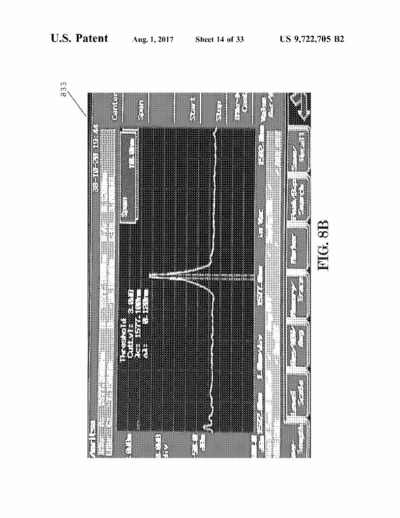
In an aspect of the present disclosure, a remote operator may have complete control of parameter settings of the tunable laser, via various graphical user interfaces (GUIs) configured to communicate through embedded processes in the field programmable device 103 or 531 (e.g., FPGA or PLD or the like) to the laser current and temperature settings of the tunable laser. For example, the remote operator may change various parameter settings at different temperature settings and observe optical output spectra. In the example, FIGS. 8A-11B show GUIs that may be configured to control the laser current and temperature settings at 23°C., 30° C. and 40°C., with respective output spectra under the control of an operator via the GUIs.
In one implementation, the GUI function may be inte grated in the field programmable device or a system includ ing the field programmable device, connected to the system via one or more wireless techniques, or connected to the system over optical transmission line(s) from a remote site or location. In particular, the GUI control function may be performed at the system via one or more communication interfaces including API, I2C, GPIO, or etc. of an optical transmitter (or transceiver). Also, one or more control sig nals may be supplied from a GUI of the system, a GUI connected to the system via one or more wireless techniques, or a GUI connected to the system over optical transmission
US 9,722,705 B2 17
line(s) where the one or more control signals come from a GUI of another system at a remote site. Further, when the one or more control signals come from the GUI of another system at the remote site, the optical receiver of the system may read or decode input signals directly to control a wavelength of the system. Alternatively, the one or more control signals from the GUI of another system at the remote site may be received and decoded by a host coupled to the system and Subsequently issue one or more commands to control the wavelength of the system. By way of example, FIG. 8A illustrates laser current and
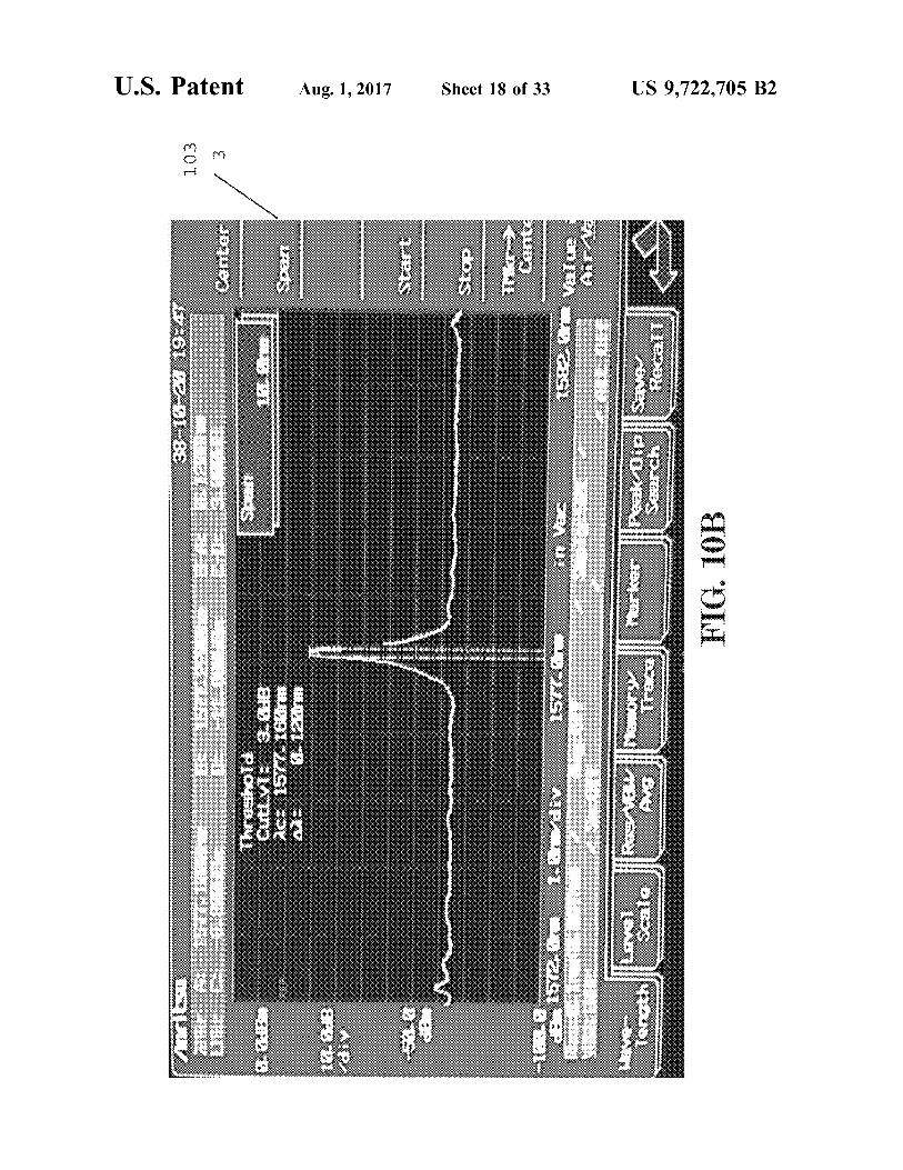
temperature settings from GUI control 831 for a temperature value of 23°C. with laser mirror current adaptation enabled, and FIG. 8B shows its corresponding optical spectrum output 833. FIG. 9A illustrates laser current and temperature settings from GUI control 931 for a temperature value of 30° C. without laser mirror current adaptation, and FIG. 9B shows its corresponding optical spectrum output 933. FIG. 10A illustrates laser current and temperature settings from GUI control 1031 for a temperature value of 30° C. with laser mirror current adaptation enabled, and FIG. 10B shows its corresponding optical spectrum output 1033. FIG. 11A illustrates laser current and temperature settings from GUI control 1131 for a temperature value of 40° C. with laser mirror current adaptation enabled, and FIG. 11B shows its corresponding optical spectrum output 1133. As noted, for the temperature values of 23°C. and 40°C.
is shown only with the current correction function enabled, whereas for 30° C. is shown laser current settings and example spectra both with and without the current correc tion. In the case of 30° C., it is noted that the optical spectrum output is centered at 1577. 160 nm with laser mirror current adaptation enabled, while the optical spec trum output is centered at 1578.040 nm without laser mirror current adaptation enabled. As such, the present disclosure may provide the operator at a remote location (e.g., at a host device) with enhanced capability to control various param eter settings of the tunable laser, as well as operational parameters relating to one or more processes concurrently running in the field programmable device, via the one or more GUIs as shown in FIGS. 8A, 9A, 10A, and 11A.
Linewidth Reduction Algorithm Digital Signal Processing
In an aspect of the present disclosure, a linewidth reduc tion algorithm may be digitally implemented as a concur rent, independent module or process in the field program mable device 103 or 531, such as the FPGA, PLD, or the like. By way of example, the linewidth reduction algorithm, such as the Pound-Drever-Hall (PDH) technique is a widely used and powerful approach for stabilizing the frequency of light from tunable lasers by locking to a stable cavity. The range of applications for the PDH technique is broad and may include interferometric gravitational wave detectors, atomic physics, and time measurement standards, many of which also use related techniques such as frequency modu lation spectroscopy.
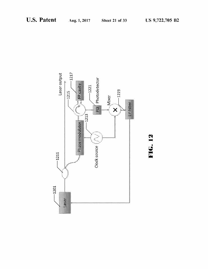
FIG. 12 illustrates a typical implementation of an analog PDH control system. The emitted light from a laser 1201 is split by a splitter 1211 by some ratio and a part is phase modulated using an external clock source 1213. The phase modulated signal is sent through a circulator 1215 and to a Fabry-Perot filter 1217, and the reflected light from the Fabry-Perot filter 1217 is detected by a photodetector 1221 and Subsequently mixed with an original clock source signal to generate an error signal 1223. The error signal 1223 is
10
15
25
30
35
40
45
50
55
60
65
18 then signal processed and used on the laser to rectify phase aberrations, thus reducing its linewidth. As noted, in an aspect of the present disclosure, a PDH feedback loop may be implemented as a concurrent, independent module or process in the field programmable device for high bit rate coherent communications as shown in FIG. 13.
In an aspect of the present disclosure, an example of a system with a 100 Gbps transmitter using a wavelength locker system as an optical detection system is illustrated in FIG. 13. The advantages of the present disclosure for linewidth narrowing or reduction, required for coherent communications and other high bit rate communications (and spectrally efficient communications systems), may include that the control circuitry may be implemented as a concurrent, independent module or process in the field programmable device 103 or 531, such as the FPGA, PLD or the like, running at a clock speed independent of other control loop processes and optimized for a desired lin ewidth. Additionally, in one implementation, the same optics, optoelectronics, analog electronics and analog-to digital circuits used for other purposes, e.g., a wavelength locker 1323, may also be dual used for the linewidth narrowing, e.g., PHD circuit 1325, thereby reducing the cost, complexity, size, weight and power of a low linewidth transceiver or transmitter, which may be implemented in accordance with an aspect of the present disclosure. Using the present technology described herein, thus, all of the building blocks of the analog PDH control system illustrated in FIG. 12 may be implemented in reprogrammable hard ware gates of the field programmable device 103 or 531. An illustration of a PDH linewidth control system that re-uses (dual use) wavelength locker components is shown in FIG. 13 with the PIC, external components and the PDH control loop.
Traditionally, PDH algorithms use analog electronics to form the filtering, demodulation and feedback portions of a noise reduction loop. These functions may be problematic to perform in a microprocessor or a microcontroller, due to certain requirements for fixed low latency in a path from a detector to a laser phase modulator. However, advantages of the present technology may provide that the field program mable device 103 Or 531 enables implementations of digital signal processing (DSP) functions as fixed, dedicated mod ules or processes, allowing precise control of latency. As such, the implementation of the PDH feedback loop in accordance with the present disclosure may result in immu nity from analog noise and electronic magnetic interference (EMI) sources and programmability which greatly simplifies calibration and optimization offeedback loop characteristics and linewidth reduction performance.
FIG. 14 shows an example block diagram illustrating one embodiment showing connections of a field programmable device (e.g., FPGA or PLD or the like) to ADC, DACs, laser and optical path, in accordance with an aspect of the present disclosure. FIG. 15 shows an example block diagram illus trating implementation of filtering function(s) embedded in a field programmable device for the PDH loop, in accor dance with an aspect of the present disclosure. In the example, the detected optical power from a reflected etalon optical path is digitized and fed into the field programmable device such as an FPGA 1531, which is configured to perform the PDH algorithm filtering, demodulation, and produce an error cancellation signal that drives the laser phase modulator in a photonic integrated circuit (PIC) 1535. The FPGA 1531 is also configured to produce a reference
US 9,722,705 B2 19
modulation frequency that drives an etalon input optical signal phase modulator through a DAC, as shown in FIG. 15.
In another aspect of the present disclosure, in the example of FIG. 15, an equation for the detected power from the etalon reflected optical signal, represented as a function of a difference between the reference modulation frequency and a representative unwanted frequency component may be derived and used, as shown in FIG. 16. In the equation, the detected power (P) includes three components, a DC term 1601, a component at a modulation frequency (error signal 1603), and a component at twice the modulation frequency (diagnostic 1605). The component at twice (2x) the modu lation frequency (diagnostic 1605) may be used for test and calibration of a system. In an example implementation of the PDH algorithm, through modulating a laser wavelength Such that side lobes occur on a highly sloped portion of a resonator response, an amplitude of the component at the modulation frequency (error signal 1603) is proportional to a difference between any extraneous frequency components and the modulation frequency, and responds oppositely to positive and negative phase perturbations, thus producing a desired error signal.
Further, in one implementation of the PDH algorithm, the error signal may be extracted and fed back to the phase modulator in the tunable laser to cancel undesired compo nents as shown in FIG. 17. Here, ADC interface logic receives a digitized power signal from the etalon reflected optical path detector. A digital FIR band pass filter centered at the modulation frequency removes the DC component and 2x modulation frequency components from the detected power signal. The band pass output is then multiplied by the modulation frequency reference, which is generated by a DDS. The result is a demodulated error signal with a component at 2x modulation frequency which is unwanted. As a result, a FIR low pass filter with cutoff at about the modulation frequency removes the unwanted 2x modulation frequency component, while leaving any error components up to the modulation frequency.
The resulting error signal goes through gain and offset blocks to provide proper amplitude and DC offset to drive the laser phase modulator, and then goes to the DAC interface logic which formats the data and sends it to the DAC. The design latency in the example path shown between the detected power from the etalon and the laser phase electrode, including the external ADC and DAC is less than 500 ns, the main contribution being from the FIR filters. Optimization of the foregoing algorithm may result in even lower latency. The reference DDS provides phase adjust ment of the modulator reference signals sent to both the demodulator and the reference phase modulator such that the response can be nulled for initial calibration. Gain and offset adjustment are also provided for the reference modulation output. FIR filter coefficients, reference frequency and phase, gains, and offsets are all programmable by the host, enabling ease of algorithm optimization, tuning and calibra tion of the tunable laser and it associated systems. As such, in an aspect of the present disclosure, the linewidth reduc tion algorithm may be digitally implemented as a concur rent, independent module or process in the field program mable device 103 or 531, such as the FPGA, PLD, or the like.
Real-time Monitoring of Parameters
Many parameters in a tunable laser/modulator require real time monitoring and feedback to dynamic control loops.
10
15
25
30
35
40
45
50
55
60
65
20 Parameters also require measurement at many operating points for calibration and analysis purposes, and the speed with which these measurements can be performed may be critical to enabling large scale production of tunable lasers.
In an aspect of the present disclosure, the present tech nology enables Such large scale production of tunable lasers. In other words, parallel architectures that may be created using field programmable devices, such as FPGAs or PLDs or the like, enable monitoring of the critical parameters and feed them back to multiple control loops simultaneously with minimal latency, whereas a microprocessor or micro controller would have to process and distribute all of the information in a serial and/or sequential manner. As noted above, a field programmable device-centric
implementation (e.g., FPGA/PLD-centric implementation) may be described as one embodiment of the present disclo Sure. Of parameter monitoring, the field programmable device (103, 531, etc.) may be configured to control read cycles to a plurality of ADC channels, e.g., 24 ADC chan nels, such that the channel reads occur with minimal over head and yet are fully programmable as to sequence and frequency per channel. This aspect of the present disclosure may enable monitoring of parameters critical to real time control loops with frequencies high enough to provide data for real time controls, such as wavelength locking, power control and temperature control. Table 1 below lists some of the real-time controls as well as calibration algorithms with representative parameters that need to be monitored for each and sample rates.
TABLE 1.
Real-time Controls and Functions with Representative Parameters
Sample Function Parameters Rates
Wavelength Locking Output Power 1 KHZ Etalon Transmitted Power 1 KHZ Etalon Reflected Power 1 KHZ
Automatic Power Control Output Power 100 Hz MZM Output 1 Power 100 Hz MZM Output 2 Power 100 Hz
Temperature Control Thermistor Voltage 10 Hz Linewidth Reduction Etalon Reflected Power 20 MHz
Etalon Transmitted Power 1 Laser Gain Voltage SOA1 Voltage SOA2 Voltage MZM Output 1 Power MZM Output 2 Power Mod Bias P Voltage Mod Bias N Voltage
Wavelength Calibration
Modulator Calibration K H Z.
As can be seen from Table 1 above, two things may be noted: (i) some parameters need to be sourced by more than one function; and (ii) Some parameters need to be sampled much faster than others. Thus, one or more implementations based on field programmable devices, in accordance with aspects of the present disclosure, may allow the flexibility to architect the monitoring functions in a way that maximizes efficiency and allows all processes to obtain required data at Sufficient rates simultaneously.
FIG. 18, for example, illustrates an example block dia gram of firmware control of a field programmable device 1831, e.g., FPGA/PLD firmware, and attached ADCs and DACs 1833 that are used for monitoring parameters. In the example, all real time control loops may be configured to run in parallel with independent rates, e.g., independent clock rates (for example, 10 Khz, 6.25 Khz, 100 Mhz. 1 Khz, and 20 Mhz in FIG. 18). Parameters required by the real time
US 9,722,705 B2 21
control loops may be Supplied by monitor and control logic 1835, which may be configured to access parameters through one or more SPI busses 1837 interfaced to ADCs, DACs and other devices. Further, the field programmable device 1831, e.g., FPGA, PLD, or the like, is configured to allow creating multiple SPI interfaces, each with different protocols, for devices that need high priority access, while also maximizing bandwidth and running with near-Zero overhead on the SPI interfaces shared by multiple devices. Furthermore, the parameters required by multiple control loops may be distributed simultaneously to all required functions, and the parameters that are required with high bandwidth by some functions but not others may be supplied from multiple monitoring devices, as required. As a result, in an aspect of the present disclosure, the real
time control functions may be implemented in the field programmable device 1831 as one or more concurrent, independent processes in the field programmable device 1831, and thus may be used to analyze the parameters received from the monitor and control logic 1835 and generate alarms and status which are fed back to a host via a host or register interface 1841 and/or discrete 1843. Further, in the example, the generated alarms may include: (i) laser temperature yellow and red alarms; (ii) laser power yellow and red alarms; (iii) laser on; and (iv) lambda stable. Further, in another aspect, the field programmable device 1831 may also allow the calculations and decision processes for alarms to run in parallel, minimizing the latency of reporting anomalous conditions to the host.
Wavelength Locking
A wavelength locking algorithm dynamically tunes a laser wavelength to maintain it at a precise set point over varia tions in operating conditions based on a response of a Fabry-Perot etalon. Typically, the etalon has peak responses at wavelengths and intervals coincident with standard ITU specifications, but in principle the wavelengths could be at any value or interval, depending on the design of the etalon.
FIG. 19 shows an example of general etalon reflected and transmitted responses. The transmitted response 1901 has peaks at the wavelengths of interest, whereas the reflected response 1903 has minima at these same wavelengths. In order to create an etalon geometry physically small enough to be placed with other optics in a pluggable module, compromises may be made on the finesse, or sharpness of the etalon maxima and minima, lessening the precision with which wavelength locking may be performed. In an aspect of the present disclosure, efficient measurement of etalon response and algorithmic processing of the measurements are enabled to improve the quality of the results.
In order to find the etalon peak and/or minimum corre sponding to a desired operating wavelength, the laser is first tuned to near a correct wavelength by tuning the mirrors based on a pre-calibrated table of mirror current values and corresponding wavelengths. The wavelength locking algo rithm then fine-tunes the wavelength by dithering a laser phase electrode current over a Small range about a default pre-calibrated value and searching for peak and/or minimum response. The algorithm may be performed digitally by controlling a current DAC that drives the laser phase elec trode, and monitoring the etalon response through ADCs.
FIG. 20 shows an example of a block diagram illustrating another implementation of a wavelength locking algorithm, in accordance with an aspect of the present disclosure. Here, the wavelength locking algorithm is performed digitally by controlling a current DAC 2051 that drives the laser phase
10
15
25
30
35
40
45
50
55
60
65
22 electrode, and monitoring the etalon response through ADCs 2051. In the example implementation, a phase dithering speed may be a compromise between obtaining updates to a phase offset, and hence an operating wavelength, at a sufficient rate, minimizing linewidth effects of the dithering. The example technique may step the phase at a 100 us rate. The amplitude of the dithering may also be a compromise between scanning over a wide enough range to capture the maximum/minimum and not scanning so far as to perpetuate a mode hop in the laser 2053. The scan amplitude (or range) in the example implementation may be programmable and may be set per wavelength based on calibration tables, but is generally in a range of +/-1 mA of phase electrode Current.
In an aspect, the detected etalon transmitted and reflected powers (via detectors 2058 coupled to a circulator 2055 and a etalon 2057) received from the ADC 2059 are then processed through an averaging filter 2033 to reduce noise and Smooth the response. The field programmable device 2031 such as the FPGA, PLD or the like is configured to facilitate filtering the transmitted and reflected power data in parallel. The algorithm then attempts to find a maximum in the transmitted data and a corresponding minimum in the reflected data, via a maximum/minimum search 2035, based on finding the maximum/minimum value over a data set and verifying that it is in fact an inflection point by requiring a threshold exceedance above/below the minimum/maximum at points on both sides of the minimum/maximum in the Scan. The average of the determined maximum and mini mum points is then used as a new phase offset to be applied to the laser 2053 to set a fine adjustment of the wavelength. If the algorithm fails to find an acceptable minimum or maximum, the new phase offset will be based on the inflection point successfully determined, or if neither a minimum nor maximum is determined, the data for the current scan is not used and the phase is not changed until a successful scan is obtained. The new phase offset is provided to a phase offset 2037 and to the laser 2053 via a DAC control 2039 and a current DAC 2051. Further, it is noted that the above wavelength locking algorithm may be implemented as one or more concurrent, independent pro cesses in the field programmable device (103, 531, or the like), such as the FPGA, PLD or the like.
Further, it is noted that phase modulation may be needed to achieve at least one or more of the following: (i) wave length locking, (ii) linewidth reduction; and (iii) Brillioun scattering mitigation. By way of example, in the one imple mentation, the laser wavelength is tuned under control of the field programmable device such as the FPGA or PLD or the like, via a multi-channel current DAC driving the laser electrodes, interfaced via SPI. The initial mirror and phase electrode currents for a commanded wavelength may be set via a lookup table, and a wavelength locking control loop may run continuously based on detected etalon power to maintain wavelength stability. As such, the field program mable device (e.g., FPGA, PLD, or the like) based imple mentation of real time control algorithms facilitates enhancements and optimization, as individual control loops can be tuned independently without impacting overall sys tem performance and timeline.
Temperature Control
In another aspect of the present disclosure, a process for temperature control of a tunable laser may be implemented as a concurrent, independent process in the field program mable device (e.g., FPGA/PLD) which is configured to run
US 9,722,705 B2 23
at a different clock signal from other processes. FIG. 21 illustrates an example diagram of one implementation of the temperature control process. By way of example, a module 2129 (e.g., temp pid) monitors and controls an attached TEC 2131 through a TEC controller 2135 using a discrete PID loop. It may be configured to accept desired temperature as an input and servos at a settable sample rate (the time constant) until the TEC actual temperature is the same as the set temperature. The module 2129 (e.g., temp pid) monitors the TEC
temperature, comparing it to the set temperature (e.g., tem perature setpoint) and adjusting the TEC drive current to achieve the desired temperature. The TEC 2131 may be controlled through a linear control chip. As such, tempera tures may be monitored via localized thermistors and selected ADC channel(s). TEC drive current may also be monitored via the linear control chip and selected ADC channel(s). TEC drive current may also be computed based on a PID loop output, the set temperature, and an actual TEC temperature. The PID loop output thus drives a selected DAC channel which determines the controller output cur rent. As noted above, the module 2129 (e.g., temp pid) is
configured to monitor and control an attached TEC 2131 through a TEC controller circuit 2135. The module 2129 may be configured to accept a desired temperature value as an input and servos at a settable rate (the time constant) until TEC actual temperature becomes the same as the set tem perature. Maximum TEC current as well as maximum and minimum temperature may also be monitored for alarm conditions which are indicated with red and yellow alarm outputs. The algorithm used for the servo may include a PID loop using the following discrete time domain formula:
where u(k) is the output, u(k-1) is the previously computed output, e(k) is the difference between the set temperature and
actual temperature, y(k), y(k-1), y(k-2) are the one and two sample delayed input
temperature from TEC controller. Also, values a0, a1, a2, a3 may be derived from the PID
coefficients Kp, Ki, Kd and the sample period Ts as follows:
The structure of the ALU used to generate u(k) may consist of a 16x16 multiplier with a 4:1 x 16 mux on each input followed by a 36 bit summer with an accumulator register. A 16 bit substractor block produces the e(k) value. u(k) and u(k-1) are range checked and limited to x"1000 to avoid windup or overflow. The accumulator becomes the u(k-1) value for the next iteration. The input mux and multiplier and the ALU are all pipelined and it may take 2 clocks for the first product and Sum and one clock each for the Subsequent 3 multiply-and-adds. The accumulator then may hold u(k), which is u(k-1) for the next cycle.
In an aspect of the present disclosure, there may be two indicators of errors: a red alarm and a yellow alarm. A red alarm may indicate that either a maximum temperature, current, or temperature margin has been exceeded. After an initial period of suppressing the TEC shutdown, if a red alarm occurs to allow the PID loop time to achieve the set
5
10
15
25
30
35
40
45
50
55
60
65
24 temperature, a red alarm will cause a TEC shutdown and a laser shutdown. There may be a plurality of procedures as follows: TEC init proc: When TEC is initially enabled, red alarm
shutdown is Suppressed for a period of time propor tional to the sample period, but no less than about 5.8 seconds.
Temp control: Sets and monitors alarm limits, current limits, and PID limits.
PID proc: A finite state machine (FSM) that controls PID ALU initialization and sequencing of PIDALU.
Pid impy inst: An instance of an embedded parallel signed 16x16 multiplier with a synchronizing 32 bit output register. It may be part of the PIDALU.
Local CLK Proc: Programmable sample clock generator in increments of 100 uS.
Further, in an aspect of the present disclosure, the PID constants and sample period may be estimating and set. The PID constants may be estimated using a Ziegler-Nichols method, which may require knowledge of a frequency at which the control loop will oscillate given Sufficient gains without differential or integral terms. Further, due to safety limits imposed on the design, it may not be possible to obtain this value which requires steady state oscillation. Instead, Tu may be estimated from a damped oscillation period and Ku may be estimated.
In an aspect of the present disclosure, a simple first order model of the TEC (a single coefficient low pass filter) and the PID servo may be created in a spreadsheet with the discrete coefficients, a0-a3 derived from the PID values. A step change in a set point for the temperature may generate a step response of the loop with the selected PID constants, Kp, Ki, and Kd, and the sample period Ts and the model transfer coefficient, “xfer coeff. The response may be graphed so that the results may be viewed interactively. Actual coefficient inputs to the PID module may also be multiplied by 128, allowing for a binary point at bit 6 and fractional coefficients. Additionally, the Ziegler-Nichols table may be implemented to give staring values for the PID constants given the estimates of Ku and Tu.
Further, there may be two panes in a spreadsheet for computing variables. The first pane may be used to discover Ku and Tu interactively; the second pane may be used to interactively develop optimal Kp and Ki for the SFP (the differential term has been set to zero). Further, in an aspect of the present disclosure, the Ziegler-Nichols method may assign PID coefficients based on experimental data or simu lated plant behavior using the following technique:
Set the Ki and Kd coefficients to zero. Increase the Kp (gain) coefficient until the loop oscillates
with a constant amplitude. Note the period of oscillation this is Tu in the table
below. Note the Kp gain value—this is Ku, the ultimate gain in
the table below.
control type Kp Ki Kd
P OSKu PI O45Ku 1.2Kp/Tu PD O.8Ku KpTu?2 PID 0.6Ku 2Kp/Tu KpTu/8 Pessen Integral O.7Ku 2.5Kp/Tu 0.15KpTu Some overshoot O.33Ku 2Kp/Tu KpTu/3 no overshoot 0.2Ku 2Kp/Tu KpTu/3
Note
that the spreadsheet “Ku, Tu' worksheet may be used to find the Ku and then Tuvalues after the sample rate and first order filter coefficient are selected.

US 9,722,705 B2 25
Boxcar Filter
In an aspect of the present disclosure, one or more multichannel moving average (also known as 'boxcar) filters may be digitally implemented in the field program mable device (e.g., FPGA or PLD), which may be config ured to provide configurable low pass filtering for each of 24 ADC channels in the 10G TOSA electronics board, for example. Each of the 24 channels may be set to a different filter depth of 0, 1, 2, 4, 8, 16, 32, 64, 128, or 256 samples. This capability may enable filtering of ADC output data where needed for short term fluctuations or random higher frequency noise. Filter depth and enable may also be pro grammed through a set of channel number associated reg isters in the register memory space. Before filtered output is determined to be valid, the sample memory for a given filter channel must be full of samples. As such, in one implemen tation, as the samples are taken, a sum of all the samples and the new sample minus the oldest sample may be averaged and presented as an output value of the filter.
In an aspect of the present disclosure, one or more boxcar filters may be implemented using internal memory blocks of the field programmable device (e.g., FPGA or PLD) for data history storage, addressing and indexing, and accumulating Sums for each channel. By way of example, a single 24-bit ALU in the field programmable device may be used for data Summing and Sums may be shifted right a number of positions appropriate for the depth of each filter. In one implementation, it may take approximately 10 system clock times from input to output (about 400 ns). Since a sample rate of an associated analog Subsystem may be about 4 KHZ/channel, the boxcar filter may easily accommodate all channels while adding very little delay time. A block dia gram for a symbolic model of one channel of the boxcar filter is shown in FIG. 22.
Non-Volatile Memory Storage
In an aspect of the present disclosure, a state of the registered memory map as well as device wavelength tables may be stored in one or more non-volatile flash memories (e.g., a Mcronix flash memory, MX25L4006E). Each flash memory may be a 4 Mb capacity device and may be integral during the power-up of the device to apply the proper personality and in maintaining end user defined behavior of an entire system. There may be a set of registers which when written to, cause an immediate writing of that byte to the flash. Therefore, when power is cycled, that byte data may persist, maintaining the user defined personality. An example of the address space of the non-volatile flash memory may be defined as shown in FIG. 23A. Also, a wavelength definition table may be defined as shown in FIG. 23B. Each wavelength table may be a 32 byte structure, and each device may include storage space for a number of wavelength tables, whether internal or external to the field programmable device.
Power-Up Flash Procedures to Populate Registers and Wavelength Tables
In an aspect of the present disclosure, upon power up of an optical communication system or a device, on board firmware personality may undergo two procedures in order to place the device in a state determined by an end user. For example, the procedures may include a loading of the registered memory map into a firmware system and a copying of the wavelength tables into RAM storage of the
10
15
25
30
35
40
45
50
55
60
65
26 communication system. Each of the memory spaces may be defined as 4096 bytes (4 KB). As shown in the flash memory map in FIG. 23A, the register memory map may begin at 0x70000. Upon the power up, the first procedure performed by the on board firmware personality is to copy the register values into the firmware register space. The second proce dure performed is the copying of the wavelength tables from the flash beginning at 0x71000 into the wavelength RAM space on the device. Once all of the memory has been copied from the flash, the register value for a "current wavelength” is read by the device, and that wavelength is written to the laser electrode registers. At this point, the device may be fully powered up and configured, with the selected wave length loaded and ready for operation. In the implementa tion, it may take approximately 0.4 ms to copy all of the register and wavelength data from the flash storage device.
Applications Programming Interface (API)
In an aspect of the present disclosure, the Applications Programming Interface (API) may be implemented by DLL executable libraries. By importing the API DLLs into a coding project, a user of the API may have access to functions that control a tunable laser control electronics. The API functions available to the user may allow one to properly open a serial communications port, read and write to the register interface, and even provide some higher level macro functions to directly read the device temperature, set electrode currents, read monitor Voltages, set a wavelength, and turn the laser and laser TEC on and off. As such, the present disclosure may provide software-enabled features accessible via the APIs, offering extensive real-time control and monitoring of one or more modules or processes based on, for example, actual traffic flows. As noted, such pro grammability provides an unprecedented level of flexibility and responsiveness at an optical layer with real-time scaling and rerouting of a bandwidth, a higher bandwidth extraction from a given fiber plant as well as a reduction in complexity and related cost of planning, building, operating and main taining data networks.
While the foregoing written description of the present disclosure enables one of ordinary skill to make and use what is considered presently to be the best mode thereof, those of ordinary skill will understand and appreciate the existence of variations, combinations, and equivalents of the specific embodiment, method, and examples herein. The present disclosure should therefore not be limited by the above described embodiment, method, and examples, but by all embodiments and methods within the scope and spirit of the present disclosure.
Various aspects of the present disclosure may also be implemented by one or more processing systems. For example, the host controller 101, field programmable device 103, or laser 109 may be implemented with a bus architec ture, which may include a bus and any number of intercon necting buses and bridges, as shown in FIG. 24. The bus links together various circuits including one or more pro cessing systems, one or more memories, one or more communication interfaces, and input/output devices. The one or more processing systems are responsible for manag ing the bus and general processing, including the execution of software stored on the non-transitory computer-readable medium. As noted, the one or more processing systems may include one or more reconfigurable circuit blocks that inter pret and execute instructions. In the example implementa tions, the one or more processing systems may be imple mented as or include one or more application specific
US 9,722,705 B2 27
integrated circuits, field programmable logic arrays, or the like. The software, when executed by the one or more processing systems, causes the one or more processing systems to perform the various functions described herein for any particular apparatus. The non-transitory computer readable medium may also be used for storing data that is manipulated by the one or more processing systems when executing Software. The one or more memories may include various types of memories including a random access memory or a read only memory, and/or other types of magnetic or optical recording medium and its corresponding derive for storing information and/or instructions. The one or more input/output devices may include devices that permit inputting information and/or outputting information to an external device or equipment. The one or more communication interfaces may also include any transceiver like mechanism that enables communication with other devices and/or systems, including optical transceivers (e.g., TOSA and/or ROSA).
Even though particular combinations of features are dis closed in the specification and/or recited in the claims, these combinations are not intended to limit the disclosure of the present technology. Further, the methods or methodologies for the present technology disclosed herein may be imple mented in Software, hardware, any combinations of software and hardware, a computer program or firmware incorporated in a computer readable medium for execution by a process ing system that includes discrete hardware circuits, gated logic, state machines, programmable logic devices (PLDS), field programmable gate arrays (FPGAs), application spe cific integrated circuits (ASICs), and other suitable hardware configured to perform various functions described herein. The term “software.” “module,” or “process' used herein
is to be construed broadly to mean any instructions, instruc tion sets, programs, Subprograms, code, program code, Software modules, applications, software packages, routines, objects, executables, threads of execution, procedures, func tions, etc. including firmware, microcode, middleware, Soft ware, hardware description language, or the like. Also, the Software may include various types of machine instructions including instructions, code, programs, Subprograms, soft ware modules, applications, Software packages, routines, Subroutines, executables, procedures, functions, etc. Further, the software may also refer to general Software, firmware, middleware, microcode, hardware description language, or etc. As noted above, the software may be stored on a computer-readable medium.
Examples of a computer-readable medium may include a non-transitory computer-readable medium, Such as, by way of example, an optical disk, a magnetic storage device, a digital versatile disk, a flash memory, random access memory (RAM), static random access memory (SRAM), synchronous dynamic random access memory (SDRAM), read only memory (ROM), a register, programmable ROM (PROM), erasable PROM (EPROM), electrically erasable PROM (EEPROM), a removable disk, a flash memory device, and any other Suitable medium for storing software that may be accessed and read by a processor or a processing system. It is also appreciated that one skilled in the art will recognize how best to implement the described functionality relating to various functions that are to be implemented in one or more field programmable device standalone or in combination with one or more computing systems, depend ing upon a particular application within design constraints. The term “unit' or “component used herein means
Software, hardware, or any combinations thereof. A compo nent may be implemented as a Software component, a
10
15
25
30
35
40
45
50
55
60
65
28 hardware component, or any combinations thereof, includ ing a field programmable gate array (FPGA), digital logic, digital logic arrays, application specific integrated circuit (ASIC), digital signal processor (DSP), etc. or any combi nations thereof. The component thus may include software components, task components, processes, procedures, func tions, program code, firmware, micro-codes, circuits, data structures, tables, arrays, and variables. While for the purpose of simplicity the methodologies are
described herein as a series of steps or acts, it is to be understood that the claimed subject matter is not limited by the order of steps or acts, as some steps or acts may occur in different orders and/or concurrently with other acts from that shown and described herein. Further, not all illustrated steps or acts may be required to implement various meth odologies according to the present technology disclosed herein. Furthermore, the methodologies disclosed herein and throughout this specification are capable of being stored on an article of manufacture to facilitate transporting and transferring Such methodologies to one or more processing systems. The term “article of manufacture' as used herein is intended to encompass a computer program accessible from any computer-readable device, carrier, or medium. The terms “first,” “second, and so forth used herein may
be used to describe various components, but the components are not limited by the above terms. The above terms are used only to discriminate one component from the other compo nent. For example, without departing from the scope of the present disclosure, a second component may be referred to as a first component, and the first component may be referred to as the second component in a similar manner. Also, the term “and/or used herein includes a combination of a plurality of associated items or any item of the plurality of associated items.
Further, it is to be noted that when it is described that an element is “coupled or “connected to another element, the element may be directly coupled or directly connected to the other element, or the element may be coupled or connected to the other element through a third element. A singular form may include a plural form if there is no clearly opposite meaning in the context. In the present disclosure, the term “include’ or “have' used herein indicates that a feature, an operation, a component, a step, a number, a part or any combination thereof described herein is present. However, the term “include or “have does not exclude a possibility of presence or addition of one or more other features, operations, components, steps, numbers, parts or combina tions. Also, as used herein, the article “a” is intended to include one or more items. Further, no element, act, step, or instruction used in the present disclosure should be con Strued as critical or essential to the present disclosure unless explicitly described as such in the present disclosure.
Although the present technology has been illustrated with specific examples described herein for purposes of describ ing example embodiments, it is appreciated by one skilled in the relevant art that a wide variety of alternate and/or equivalent implementations may be substituted for the spe cific examples shown and described without departing from the scope of the present disclosure. As such, the present disclosure is intended to cover any adaptations or variations of the examples and/or embodiments shown and described herein, without departing from the spirit and the technical Scope of the present disclosure.

US 9,722,705 B2 29
What is claimed is: 1. An apparatus for controlling, monitoring, and/or com
municating with an optical device, photonic integrated cir cuit or Subassembly, the apparatus comprising:
an optical device including a tunable laser having two mirrors; and
a field programmable device including programmable hardware gates coupled to the optical device,
wherein the field programmable device is configured to act as a control device for the apparatus and to imple ment a plurality of functions at a gate level for con trolling, monitoring, and/or communicating with the optical device, each of the plurality of functions being configured to run as a concurrent process within the field programmable device;
wherein the plurality of functions includes functions to obtain one or more gain-Voltage maps by tuning laser mirror currents of the tunable laser at a temperature value; and
wherein the plurality of functions further includes func tions to determine lasing wavelengths corresponding to minima of the one or more gain-Voltage maps, the lasing wavelengths being used for tuning or calibrating the tunable laser of the optical device.
2. The apparatus of claim 1, wherein the plurality of functions is configured to run at different clock signals in the field programmable device.
3. The apparatus of claim 1, wherein the minima of the one or more gain-Voltage maps are determined as points of maximum power output of the tunable laser.
4. The apparatus of claim 1, wherein the field program mable device is configured to control one or more elements of the optical device which is selected from the group consisting of an optical data modulator/demodulator, inter nal or external optical and optoelectronic monitoring and control functions.
5. The apparatus of claim 4, wherein the field program mable device comprises one or more field programmable gate arrays (FPGAs) or programmable logic devices (PLDs).
6. The apparatus of claim 1, wherein the field program mable device is configured to automatically adapt laser control currents of the tunable laser to measure a tempera ture so as to reduce a load on a thermoelectric cooler (TEC), based on the measured temperature and at least one of by moving between tables stored in the field programmable device or by extrapolating between temperature wavelength maps.
7. The apparatus of claim 1, wherein the field program mable device is configured to run one or more functions selected from the group consisting of:
control and/or monitoring of a laser output power of the tunable laser;
(ii) control and/or monitoring of temperature sensitive components in connection with the optical device;
(iii) control and/or monitoring of a laser wavelength of the tunable laser;
(iv) control of a wavelength locker function; and (V) control and/or monitoring of one or more communi
cation interfaces coupled to a host. 8. The apparatus of claim 1, wherein the optical device
comprises a communication interface which is integrated into the field programmable device, preferably wherein the programmable device comprises a field programmable gate array (FPGA).
9. The apparatus of claim 8, wherein the communication interface comprises one or more of Sockets to a graphical user interface (GUI) or an application programming inter
5
10
15
25
30
35
40
45
50
55
60
65
30 face (API) that allows control, monitoring and/or commu nication with the tunable laser, an optical data modulator/ demodulator, or other optical or optoelectronic elements which are monolithically integrated.
10. The apparatus of claim 9, wherein a software layer is used to interact with the tunable laser through the field programmable device to implement a fast wavelength cali bration algorithm.
11. The apparatus of claim 1, wherein the field program mable device is configured to determine a temperature dependence of the mirror currents of the tunable laser based on the one or more gain-Voltage maps, and to automatically adapt the laser mirror currents based on the one or more gain-Voltage maps at different temperatures.
12. The apparatus of claim 1, wherein the plurality of functions includes a Pound-Drever-Hall (PDH) algorithm for reducing a linewidth and/or stabilizing a frequency of light from the tunable laser of the optical device.
13. The apparatus of claim 12, wherein the PDH algo rithm is implemented in reprogrammable hardware gates of the field programmable device and some of the reprogram mable hardware gates are used for implementing a wave length locking function.
14. The apparatus of claim 13, wherein the reprogram mable hardware gates of the field programmable device are configured to implement at least one of host communica tions interfaces, a memory map, wavelength memory and management, programmable read-only memory (PROM) - serial peripheral interface (SPI) Flash interface to external erasable programmable read-only memory (EPROM), set currents and voltages to the optical device, monitoring of optical and electronic components, boxcar averagers, auto matic power control, wavelength locking, linewidth narrow ing algorithms, temperature monitoring and control, alarm generation, monitoring, control and communication of sta tuses, and application programmable interfaces.
15. The apparatus of claim 1, wherein the field program mable device is configured to receive one or more control signals from a graphical user interface (GUI) coupled to the apparatus via wireless communications or from a GUI of another apparatus located at a remote site over an optical communication link.
16. An optical communication system comprising: an optical device including a tunable laser integrated on a
same Substrate with an optical modulator and a semi conductor optical amplifier, non-integrated optical and optoelectronic elements; and
a field programmable device including programmable hardware gates coupled to the optical device and a laser transmitter and receiver,
wherein the field programmable device is configured to act as a control device for the optical communication system and to implement a plurality of functions at a gate level for controlling, monitoring, and/or commu nicating with the optical device, each of the plurality of functions being configured to run as a concurrent process, within the field programmable device;
wherein the plurality of functions includes functions to obtain one or more gain-Voltage maps based on laser mirror currents of the tunable laser at a temperature value; and
wherein the plurality of functions further includes func tions to determine lasing wavelengths corresponding to minima of the one or more gain-Voltage maps, the lasing wavelengths being used for tuning or calibrating the tunable laser of the optical device.

US 9,722,705 B2 31
17. The optical communication system of claim 16, wherein the field programmable device comprises one or more field programmable gate arrays (FPGAs) or program mable logic devices (PLDs).
18. The optical communication system of claim 17, wherein the field programmable device is configured to comprise application programmable interfaces (APIs) for real-time control and monitoring of the optical device based on actual traffic flows.
19. The optical communication system of claim 16, wherein the plurality of functions is configured to run at different clock signals in the field programmable device.
20. The optical communication system of claim 16, wherein the field programmable device comprises a com munication interface including one or both of sockets to a graphical user interface (GUI) or an application program ming interface (API) that allows control, monitoring and/or communication with the tunable laser integrated on the same substrate with the optical modulator and the semiconductor
10
15
optical amplifier, non-integrated optical and optoelectronic 20 elements.
32