Embed Size (px)
Citation preview
10.7 Gbps Active Back-Termination, Differential Laser Diode Driver
Data Sheet ADN2525
Rev. B Document Feedback Information furnished by Analog Devices is believed to be accurate and reliable. However, no responsibility is assumed by Analog Devices for its use, nor for any infringements of patents or other rights of third parties that may result from its use. Specifications subject to change without notice. No license is granted by implication or otherwise under any patent or patent rights of Analog Devices. Trademarks and registered trademarks are the property of their respective owners.
One Technology Way, P.O. Box 9106, Norwood, MA 02062-9106, U.S.A.Tel: 781.329.4700 ©2005–2017 Analog Devices, Inc. All rights reserved. Technical Support www.analog.com
FEATURES Up to 10.7 Gbps operation Very low power: 670 mW (IBIAS = 40 mA, IMOD = 40 mA) Typical 24 ps rise/fall times Full back-termination of output transmission lines Compatible with XMD-MSA TOSA Drives TOSAs with resistances ranging from 5 Ω to 50 Ω PECL-/CML-compatible data inputs Bias current range: 10 mA to 100 mA Differential modulation current range: 10 mA to 80 mA Automatic laser shutdown (ALS) 3.3 V operation Compact 3 mm × 3 mm LFCSP Voltage input control for bias and modulation currents XFP-compliant bias current monitor Optical evaluation board available
APPLICATIONS SONET OC-192 optical transceivers SDH STM-64 optical transceivers 10 Gb Ethernet optical transceivers XFP/X2/XENPAK/XPAK/MSA 300 optical modules SR and VSR optical links
GENERAL DESCRIPTION
The ADN2525 laser diode driver is designed for direct modula-tion of packaged laser diodes having a differential resistance ranging from 5 Ω to 50 Ω. The active back-termination technique provides excellent matching with the output transmission lines while reducing the power dissipation in the output stage. The back-termination in the ADN2525 absorbs signal reflections from the TOSA end of the output transmission lines, enabling excellent optical eye quality to be achieved even when the TOSA end of the output transmission lines is significantly misterminated. The small package provides the optimum solution for compact modules where laser diodes are packaged in low pin-count optical subassemblies.
The modulation and bias currents are programmable via the MSET and BSET control pins. By driving these pins with control voltages, the user has the flexibility to implement various average power and extinction ratio control schemes, including closed-loop control and look-up tables. The automatic laser shutdown (ALS) feature allows the user to turn on/off the bias and modulation currents by driving the ALS pin with the proper logic levels.
The product is available in a space-saving 3 mm × 3 mm LFCSP specified from −40°C to +85°C.
FUNCTIONAL BLOCK DIAGRAM
50Ω
200Ω
800Ω
200Ω 2Ω
VCCDATAP
DATAN
MSET GND BSET
IBMON
IBIAS
IMODP
IMODN
ADN2525
VCC ALS
GND
VCC
VCC
50Ω 50Ω
200Ω
800Ω
IMOD
0507
7-00
1
Figure 1.

ADN2525 Data Sheet
Rev. B | Page 2 of 16
TABLE OF CONTENTS Features .............................................................................................. 1
Applications ....................................................................................... 1
General Description ......................................................................... 1
Functional Block Diagram .............................................................. 1
Revision History ............................................................................... 2
Specifications ..................................................................................... 3
Thermal Specifications ................................................................ 4
Absolute Maximum Ratings ............................................................ 5
ESD Caution .................................................................................. 5
Pin Configuration and Function Descriptions ............................. 6
Typical Performance Characteristics ............................................. 7
Theory of Operation ........................................................................ 9
Input Stage ..................................................................................... 9
Bias Current ...................................................................................9
Automatic Laser Shutdown (ALS) ........................................... 10
Modulation Current ................................................................... 10
Load Mistermination ................................................................. 12
Power Consumption .................................................................. 12
Applications Information .............................................................. 13
Typical Application Circuit ....................................................... 13
Layout Guidelines....................................................................... 13
Design Example .......................................................................... 14
Outline Dimensions ....................................................................... 15
Ordering Guide .......................................................................... 15
REVISION HISTORY
4/2017—Rev. A to Rev. B Changed CP-16-3 to CP-16-22 .................................... Throughout Updated Outline Dimensions ....................................................... 15 Changes to Ordering Guide .......................................................... 15
8/2006—Rev. 0 to Rev. A Changes to Format ............................................................. Universal Changes to Features and Figure 1 ................................................... 1 Changes to Table 1 ............................................................................ 3 Changes to Table 3 ............................................................................ 5 Changes to Figure 19 ........................................................................ 9 Changes to Figure 25 ...................................................................... 10 Changes to Modulation Current Section and Figure 29 ........... 11 Changes to Typical Application Circuit Section......................... 13 Changes to Ordering Guide .......................................................... 15
3/2005—Revision 0: Initial Version

Data Sheet ADN2525
Rev. B | Page 3 of 16
SPECIFICATIONS VCC = VCCMIN to VCCMAX, TA = −40°C to +85°C, 50 Ω differential load resistance, unless otherwise noted. Typical values are specified at 25°C, IMOD = 40 mA.
Table 1. Parameter Min Typ Max Unit Test Conditions/Comments BIAS CURRENT (IBIAS)
Bias Current Range 10 100 mA Bias Current while ALS Asserted 100 µA ALS = high Compliance Voltage1 0.6 VCC – 1.2 V IBIAS = 100 mA
0.6 VCC – 0.8 V IBIAS = 10 mA MODULATION CURRENT (IMODP, IMODN)
Modulation Current Range 10 80 mA diff RLOAD = 5 Ω to 50 Ω differential Modulation Current While ALS Asserted 0.5 mA diff ALS = high Rise Time (20% to 80%)2, 3 24 32.5 ps Fall Time (20% to 80%)2, 3 24 32.5 ps Random Jitter2, 3 0.4 0.9 ps rms Deterministic Jitter3, 4 7.2 12 ps p-p Includes pulse-width distortion Pulse-Width Distortion2, 3 2 5 ps PWD = ABS(THIGH − TLOW)/2 Differential |S22| −10 dB 5 GHz < f < 10 GHz, Z0 = 50 Ω differential −14 dB f < 5 GHz, Z0 = 50 Ω differential Compliance Voltage1 VCC − 1.1 VCC + 1.1 V
DATA INPUTS (DATAP, DATAN) Input Data Rate 10.7 Gbps NRZ Differential Input Swing 0.4 1.6 V p-p diff Differential ac-coupled Differential |S11| −16.8 dB f < 10 GHz, Z0 = 100 Ω differential Input Termination Resistance 85 100 115 Ω Differential
BIAS CONTROL INPUT (BSET) BSET Voltage to IBIAS Gain 75 100 120 mA/V BSET Input Resistance 800 1000 1200 Ω
MODULATION CONTROL INPUT (MSET) MSET Voltage to IMOD Gain 70 88 110 mA/V See Figure 29 MSET Input Resistance 800 1000 1200 Ω
BIAS MONITOR (IBMON) IBMON to IBIAS Ratio 10 µA/mA Accuracy of IBIAS to IBMON Ratio −5.0 +5.0 % 10 mA ≤ IBIAS < 20 mA, RIBMON = 1 kΩ
−4.0 +4.0 % 20 mA ≤ IBIAS < 40 mA, RIBMON = 1 kΩ −2.5 +2.5 % 40 mA ≤ IBIAS < 70 mA, RIBMON = 1 kΩ −2 +2 % 70 mA ≤ IBIAS < 100 mA, RIBMON = 1 kΩ AUTOMATIC LASER SHUTDOWN (ALS)
VIH 2.4 V VIL 0.8 V IIL −20 +20 µA IIH 0 200 µA ALS Assert Time 2 µs Rising edge of ALS to fall of IBIAS and
IMOD below 10% of nominal; see Figure 2 ALS Negate Time 10 µs Falling edge of ALS to rise of IBIAS and
IMOD above 90% of nominal; see Figure 2 POWER SUPPLY
VCC 3.07 3.3 3.53 V ICC
5 39 45 mA VBSET = VMSET = 0 V ISUPPLY
6 157 176 mA VBSET = VMSET = 0 V; ISUPPLY = ICC + IMODP + IMODN
See notes on next page.
ADN2525 Data Sheet
Rev. B | Page 4 of 16
1 Refers to the voltage between the pin for which the compliance voltage is specified and GND. 2 The pattern used is composed by a repetitive sequence of eight 1s followed by eight 0s at 10.7 Gbps. 3 Measured using the high speed characterization circuit shown in Figure 3. 4 The pattern used is K28.5 (00111110101100000101) at a 10.7 Gbps rate. 5 Only includes current in the ADN2525 VCC pins. 6 Includes current in ADN2525 VCC pins and dc current in IMODP and IMODN pull-up inductors. See the Power Consumption section for total supply current calculation.
THERMAL SPECIFICATIONS Table 2. Parameter Min Typ Max Unit Conditions/Comments θJ-PAD 2.6 5.8 10.7 °C/W Thermal resistance from junction to bottom of exposed pad θJ-TOP 65 72.2 79.4 °C/W Thermal resistance from junction to top of package IC Junction Temperature 125 °C
90%
10%
ALS
IBIASAND IMOD
ALSASSERT TIME
ALSNEGATE TIME
t
t
0507
7-00
2
Figure 2. ALS Timing Diagram
MSET NC1 ALS GND
BSET IBMON IBIAS GND
VCC
IMODP
IMODN
VCC
10nF
10nF
J8 J5
VEEVEE
TP1 10nF
ADN2525
22µF
VEE
GND
GND
GND
GND
GND
GND
GND
GND
GND
GND
GND
50Ω
50Ω
OSCILLOSCOPE
BIAS TEE: PICOSECOND PULSE LABS MODEL 5542-219ADAPTER: PASTERNACK PE-9436 2.92mm FEMALE-TO-FEMALE ADAPTERATTENUATOR: PASTERNACK PE-7046 2.92mm 20dB ATTENUATOR
ADAPTER
VBSET
Z0 = 50Ω Z0 = 25Ω Z0 = 50Ω
Z0 = 25Ω Z0 = 50ΩZ0 = 50ΩZ0 = 50Ω
Z0 = 50Ω
1kΩ
VEE
VEE
VMSET
GND GND GND
TP2
10Ω
70Ω
35Ω
35Ω
10nF GNDVEE
J2
GND GND GND
GND
VCC
VCC
DATAN
DATAP
GND
GNDGND
J3
GND GND
BIASTEE
BIASTEE
ADAPTER
ATTENUATOR
ATTENUATOR
0507
7-00
3
Figure 3. High Speed Characterization Circuit
Data Sheet ADN2525
Rev. B | Page 5 of 16
ABSOLUTE MAXIMUM RATINGS Table 3. Parameter Min Max Unit Supply Voltage, VCC to GND −0.3 +4.2 V IMODP, IMODN to GND VCC − 1 .5 4.75 V DATAP, DATAN to GND VCC − 1.8 VCC − 0.4 V All Other Pins −0.3 VCC + 0.3 V Junction Temperature 150 °C Storage Temperature Range −65 +150 °C Soldering Temperature
(Less than 10 sec) 300 °C
Stresses at or above those listed under Absolute Maximum Ratings may cause permanent damage to the product. This is a stress rating only; functional operation of the product at these or any other conditions above those indicated in the operational section of this specification is not implied. Operation beyond the maximum operating conditions for extended periods may affect product reliability.
ESD CAUTION

ADN2525 Data Sheet
Rev. B | Page 6 of 16
PIN CONFIGURATION AND FUNCTION DESCRIPTIONS
GND
IBIAS
IBMON
BSET
VCC
IMO
DN
IMO
DP
VCC
MSET
GND
ALS
NC
PIN 1INDICATOR
VCC
DA
TAN
DA
TAP
VCC
0507
7-01
6
12
11
10
1
3
4 9
2
65 7 8
16 15 14 13
ADN2525TOP VIEW
(Not to Scale)
Figure 4. Pin Configuration
Note that the exposed pad on the bottom of the package must be connected to the VCC or GND plane.
Table 4. Pin Function Description Pin No. Mnemonic I/O Description 1 MSET Input Modulation Current Control Input 2 NC N/A No Connect—Leave Floating 3 ALS Input Automatic Laser Shutdown 4 GND Power Negative Power Supply 5 VCC Power Positive Power Supply 6 IMODN Output Modulation Current Negative Output 7 IMODP Output Modulation Current Positive Output 8 VCC Power Positive Power Supply 9 GND Power Negative Power Supply 10 IBIAS Output Bias Current Output 11 IBMON Output Bias Current Monitoring Output 12 BSET Input Bias Current Control Input 13 VCC Power Positive Power Supply 14 DATAP Input Data Signal Positive Input 15 DATAN Input Data Signal Negative Input 16 VCC Power Positive Power Supply Exposed Pad Pad Power Connect to GND or VCC
Data Sheet ADN2525
Rev. B | Page 7 of 16
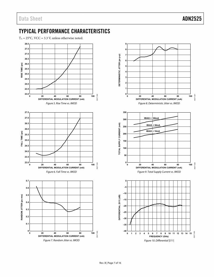
TYPICAL PERFORMANCE CHARACTERISTICS TA = 25°C, VCC = 3.3 V, unless otherwise noted.
DIFFERENTIAL MODULATION CURRENT (mA)
1000 20 40 60 80
RIS
E T
IME
(p
s)
28.0
23.5
24.0
24.5
25.0
25.5
26.0
26.5
27.0
27.5
23.005
077-
004
Figure 5. Rise Time vs. IMOD
DIFFERENTIAL MODULATION CURRENT (mA)
1000 20 40 60 80
FA
LL
TIM
E (
ps)
27.5
26.5
27.0
25.5
26.0
25.0
24.0
24.5
23.5
23.0
0507
7-00
5
Figure 6. Fall Time vs. IMOD
DIFFERENTIAL MODULATION CURRENT (mA)
1000 20 40 60 80
RA
ND
OM
JIT
TE
R (
ps
rms)
0.7
0.5
0.6
0.4
0.3
0.2
0.1
0
0507
7-00
6
Figure 7. Random Jitter vs. IMOD
DIFFERENTIAL MODULATION CURRENT (mA)
1000 20 40 60 80
DE
TE
RM
INIS
TIC
JIT
TE
R (
ps
p-p
)
9
8
7
4
3
6
5
2
1
0
0507
7-00
7
Figure 8. Deterministic Jitter vs. IMOD
DIFFERENTIAL MODULATION CURRENT (mA)
1000 20 40 60 80
TO
TA
L S
UP
PL
Y C
UR
RE
NT
(m
A)
350
300
250
200
150
100
50
0
IBIAS = 10mA
IBIAS = 50mA
IBIAS = 100mA
0507
7-00
8
Figure 9. Total Supply Current vs. IMOD
FREQUENCY (GHz)
150 1 2 3 4 5 6 7 8 9 10 11 12 13 14
DIF
FE
RE
NT
IAL
|S
11|
(dB
)
0
–40
–35
–30
–25
–20
–15
–10
–5
0507
7-00
9
Figure 10. Differential |S11|
ADN2525 Data Sheet
Rev. B | Page 8 of 16
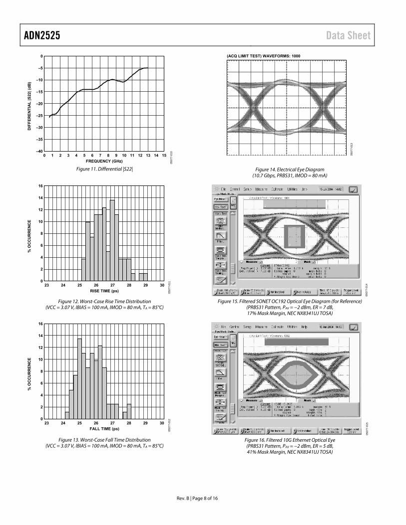
FREQUENCY (GHz)
150 1 2 3 4 5 6 7 8 9 10 11 12 13 14
DIF
FE
RE
NT
IAL
|S
22|
(dB
)
0
–40
–35
–30
–25
–20
–15
–10
–5
0507
7-01
0Figure 11. Differential |S22|
RISE TIME (ps)
3023 24 25 26 27 28 29
% O
CC
UR
RE
NC
E
16
10
12
14
6
8
4
2
0
0507
7-01
1
Figure 12. Worst-Case Rise Time Distribution (VCC = 3.07 V, IBIAS = 100 mA, IMOD = 80 mA, TA = 85°C)
FALL TIME (ps)
3023 24 25 26 27 28 29
% O
CC
UR
RE
NC
E
16
10
12
14
8
6
4
2
0
0507
7-01
2
Figure 13. Worst-Case Fall Time Distribution (VCC = 3.07 V, IBIAS = 100 mA, IMOD = 80 mA, TA = 85°C)
(ACQ LIMIT TEST) WAVEFORMS: 1000
0507
7-01
3
Figure 14. Electrical Eye Diagram (10.7 Gbps, PRBS31, IMOD = 80 mA)
0507
7-01
4
Figure 15. Filtered SONET OC192 Optical Eye Diagram (for Reference) (PRBS31 Pattern, PAV = −2 dBm, ER = 7 dB, 17% Mask Margin, NEC NX8341UJ TOSA)
0507
7-01
5
Figure 16. Filtered 10G Ethernet Optical Eye (PRBS31 Pattern, PAV = −2 dBm, ER = 5 dB, 41% Mask Margin, NEC NX8341UJ TOSA)
Data Sheet ADN2525
Rev. B | Page 9 of 16
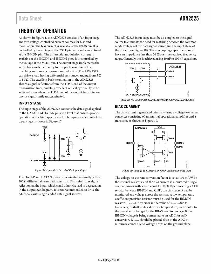
THEORY OF OPERATION As shown in Figure 1, the ADN2525 consists of an input stage and two voltage-controlled current sources for bias and modulation. The bias current is available at the IBIAS pin. It is controlled by the voltage at the BSET pin and can be monitored at the IBMON pin. The differential modulation current is available at the IMODP and IMODN pins. It is controlled by the voltage at the MSET pin. The output stage implements the active back-match circuitry for proper transmission line matching and power consumption reduction. The ADN2525 can drive a load having differential resistance ranging from 5 Ω to 50 Ω. The excellent back-termination in the ADN2525 absorbs signal reflections from the TOSA end of the output transmission lines, enabling excellent optical eye quality to be achieved even when the TOSA end of the output transmission lines is significantly misterminated.
INPUT STAGE The input stage of the ADN2525 converts the data signal applied to the DATAP and DATAN pins to a level that ensures proper operation of the high speed switch. The equivalent circuit of the input stage is shown in Figure 17.
VCC50Ω
50Ω
VCC
DATAP
DATAN
VCC
0507
7-01
7
Figure 17. Equivalent Circuit of the Input Stage
The DATAP and DATAN pins are terminated internally with a 100 Ω differential termination resistor. This minimizes signal reflections at the input, which could otherwise lead to degradation in the output eye diagram. It is not recommended to drive the ADN2525 with single-ended data signal sources.
The ADN2525 input stage must be ac-coupled to the signal source to eliminate the need for matching between the common-mode voltages of the data signal source and the input stage of the driver (see Figure 18). The ac-coupling capacitors should have an impedance less than 50 Ω over the required frequency range. Generally, this is achieved using 10 nF to 100 nF capacitors.
ADN2525
DATAP
DATANC
C50Ω 50Ω
DATA SIGNAL SOURCE
0507
7-01
8
Figure 18. AC-Coupling the Data Source to the ADN2525 Data Inputs
BIAS CURRENT The bias current is generated internally using a voltage-to-current converter consisting of an internal operational amplifier and a transistor, as shown in Figure 19.
GND
200Ω
800Ω
2Ω
R R
VCC
IBMONBSET
IBMON
ADN2525
IBIAS
200Ω
IBIAS
0507
7-01
9
Figure 19. Voltage-to-Current Converter Used to Generate IBIAS
The voltage-to-current conversion factor is set at 100 mA/V by the internal resistors, and the bias current is monitored using a current mirror with a gain equal to 1/100. By connecting a 1 kΩ resistor between IBMON and GND, the bias current can be monitored as a voltage across the resistor. A low temperature coefficient precision resistor must be used for the IBMON resistor (RIBMON). Any error in the value of RIBMON due to tolerances, or drift in its value over temperature, contributes to the overall error budget for the IBIAS monitor voltage. If the IBMON voltage is being connected to an ADC for A/D conversion, RIBMON should be placed close to the ADC to minimize errors due to voltage drops on the ground plane.

ADN2525 Data Sheet
Rev. B | Page 10 of 16
The equivalent circuits of the BSET, IBIAS, and IBMON pins are shown in Figure 20, Figure 21, and Figure 22.
VCC
BSET
VCC
800Ω
200Ω
0507
7-02
0
Figure 20. Equivalent Circuit of the BSET Pin
2Ω
2kΩ
100Ω
IBIAS
VCC
VCC05
077-
021
Figure 21. Equivalent Circuit of the IBIAS Pin
VCC
IBMON
VCC
100Ω
500Ω
VCC
0507
7-02
2
Figure 22. Equivalent Circuit of the IBMON Pin
The recommended configuration for BSET, IBIAS, and IBMON is shown in Figure 23.
ADN2525
BSET
VBSETGND
IBMON
IBIAS
TO LASER CATHODE
L
RIBMON1kΩ
IBIAS
0507
7-02
3
Figure 23. Recommended Configuration for the BSET, IBIAS, and IBMON Pins
The circuit used to drive the BSET voltage must be able to drive the 1 kΩ input resistance of the BSET pin. For proper operation of the bias current source, the voltage at the IBIAS pin must be between the compliance voltage specifications for this pin over supply, temperature, and bias current range (see Table 1). The maximum compliance voltage is specified for only two bias current levels (10 mA and 100 mA), but it can be calculated for any bias current by
VCOMPLIANCE_MAX (V) = VCC (V) − 0.75 − 4.4 × IBIAS (A)
See the Applications Information section for examples of headroom calculations.
The function of the inductor L is to isolate the capacitance of the IBIAS output from the high frequency signal path. For recommended components, see Table 6.
AUTOMATIC LASER SHUTDOWN (ALS) The ALS pin is a digital input that enables/disables both the bias and modulation currents, depending on the logic state applied, as shown in Table 5.
Table 5. ALS Logic State IBIAS and IMOD High Disabled Low Enabled Floating Enabled
The ALS pin is compatible with 3.3 V CMOS and TTL logic levels. Its equivalent circuit is shown in Figure 24.
VCC
ALS
VCC
100Ω
50kΩ2kΩ
0507
7-02
4
Figure 24. Equivalent Circuit of the ALS Pin
MODULATION CURRENT The modulation current can be controlled by applying a dc voltage to the MSET pin. This voltage is converted into a dc current by using a voltage-to-current converter using an operational amplifier and a bipolar transistor, as shown in Figure 25.
50Ω
200Ω
800Ω
MSET
GND
IMODP
IMODN
ADN2525
VCC
FROM INPUT STAGE
IMOD
0507
7-02
5
Figure 25. Generation of Modulation Current on the ADN2525
This dc current is switched by the data signal applied to the input stage (DATAP and DATAN pins) and gained up by the output stage to generate the differential modulation current at the IMODP and IMODN pins.
The output stage also generates the active back-termination, which provides proper transmission line termination. Active back-termination uses feedback around an active circuit to synthesize a broadband termination resistance. This provides

Data Sheet ADN2525
Rev. B | Page 11 of 16
excellent transmission line termination, while dissipating less power than a traditional resistor passive back-termination. No portion of the modulation current flows in the active back-termination resistance. All of the preset modulation current IMOD, the range specified in Table 1, flows in the external load. The equivalent circuits for MSET, IMODP, and IMODN are shown in Figure 26 and Figure 27. The two 25 Ω resistors in Figure 27 are not real resistors; they represent the active back-termination resistance.
VCC
MSET800Ω
200Ω
VCC
0507
7-02
6
Figure 26. Equivalent Circuit of the MSET Pin
VCC VCC
3.3Ω 3.3Ω
25Ω
IMODPIMODN
25Ω
0507
7-02
7
Figure 27. Equivalent Circuit of the IMODP and IMODN Pins
The recommended configuration of the MSET, IMODP, and IMODN pins is shown in Figure 28. See Table 6 for recommended components.
ADN2525
MSET
VMSET GND
IMODP
IBIAS
VCC
L
C
TOSA
L
IMODN
Z0 = 25Ω Z0 = 25Ω
VCC
VCC
L
C
L
Z0 = 25Ω Z0 = 25Ω
0507
7-02
8
Figure 28. Recommended Configuration for the MSET, IMODP, and IMODN Pins
The ratio between the voltage applied to the MSET pin and the differential modulation current available at the IMODP and IMODN pins is a function of the load resistance value, as shown in Figure 29.
DIFFERENTIAL LOAD RESISTANCE550 5 10 15 20 25 30 35 40 45 50
I MO
D/V M
SET
(mA
/V)
210200190180170160150140130120110100
90807060
MINIMUM
TYPICAL
MAXIMUM
0507
7-02
9
Figure 29. MSET Voltage-to-Modulation Current Ratio vs.
Differential Load Resistance
Using the resistance of the TOSA, the user can calculate the voltage range that should be applied to the MSET pin to generate the required modulation current range (see the example in the Applications Information section).
The circuit used to drive the MSET voltage must be able to drive the 1 kΩ resistance of the MSET pin. To be able to drive 80 mA modulation currents through the differential load, the output stage of the ADN2525 (the IMODP and IMODN pins) must be ac-coupled to the load. The voltages at these pins have a dc component equal to VCC and an ac component with single-ended, peak-to-peak amplitude of IMOD × 25 Ω. This is the case even if the load impedance is less than 50 Ω differential, because the transmission line characteristic impedance sets the peak-to-peak amplitude. For proper operation of the output stage, the voltages at the IMODP and IMODN pins must be between the compliance voltage specifications for this pin over supply, temperature, and modulation current range, as shown in Figure 30. See the Applications Information section for examples of headroom calculations.

ADN2525 Data Sheet
Rev. B | Page 12 of 16
IMODP, IMODN
VCC
VCC – 1.1V
VCC + 1.1V
NORMAL OPERATION REGION
0507
7-03
0
Figure 30. Allowable Range for the Voltage at IMODP and IMODN
LOAD MISTERMINATION Due to its excellent S22 performance, the ADN2525 can drive differential loads that range from 5 Ω to 50 Ω. In practice, many TOSAs have differential resistance less than 50 Ω. In this case, with 50 Ω differential transmission lines connecting the ADN2525 to the load, the load end of the transmission lines are misterminated. This mistermination leads to signal reflections back to the driver. The excellent back-termination in the ADN2525 absorbs these reflections, preventing their reflection back to the load. This enables excellent optical eye quality to be achieved, even when the load end of the transmission lines is significantly misterminated. The connection between the load and the ADN2525 must be made with 50 Ω differential (25 Ω single-ended) transmission lines so that the driver end of the transmission lines is properly terminated.
POWER CONSUMPTION The power dissipated by the ADN2525 is given by
IBIASVIV
VCCP IBIASSUPPLYMSET
13.5
where:
VCC is the power supply voltage.
IBIAS is the bias current generated by the ADN2525.
VMSET is the voltage applied to the MSET pin.
ISUPPLY is the sum of the current that flows into the VCC, IMODP, and IMODN pins of the ADN2525 when IBIAS = IMOD = 0 expressed in amps (see Table 1).
VIBIAS is the average voltage on the IBIAS pin.
Considering VBSET/IBIAS = 10 as the conversion factor from VBSET to IBIAS, the dissipated power becomes
IBIASBSET
SUPPLYMSET V
VI
VVCCP
105.13
To ensure long-term reliable operation, the junction tempera-ture of the ADN2525 must not exceed 125°C, as specified in
Table 2. For improved heat dissipation, the module’s case can be used as heat sink, as shown in Figure 31. A compact optical module is a complex thermal environment, and calculations of device junction temperature using the package θJA (junction-to-ambient thermal resistance) do not yield accurate results.
TTOP
TJ
TPAD
DIE
PACKAGE
THERMAL COMPOUND MODULE CASE
PCB
VIASCOPPER PLANE
THERMOCOUPLE
0507
7-03
1
Figure 31. Typical Optical Module Structure
The following procedure can be used to estimate the IC junction temperature:
TTOP is the temperature at top of package in °C.
TPAD is the temperature at package exposed paddle in °C.
TJ is the IC junction temperature in °C.
P is the power dissipation in W.
θJ-TOP is the thermal resistance from IC junction to package top.
θJ-PAD is the thermal resistance from IC junction to package exposed pad.
P
θJ-TOP
TPAD
TTOP
TTOP
θJ-PAD
TPAD
0507
7-03
2
Figure 32. Electrical Model for Thermal Calculations
TTOP and TPAD can be determined by measuring the temperature at points inside the module, as shown in Figure 31. The thermo-couples should be positioned to obtain an accurate measurement of the package top and paddle temperatures. Using the model shown in Figure 32, the junction temperature can be calculated by
TOPJPADJ
TOPJPADPADJTOPTOPJPADJJ
TTPT
where:
θJ-TOP and θJ-PAD are given in Table 2.
P is the power dissipated by the ADN2525.
Data Sheet ADN2525
Rev. B | Page 13 of 16
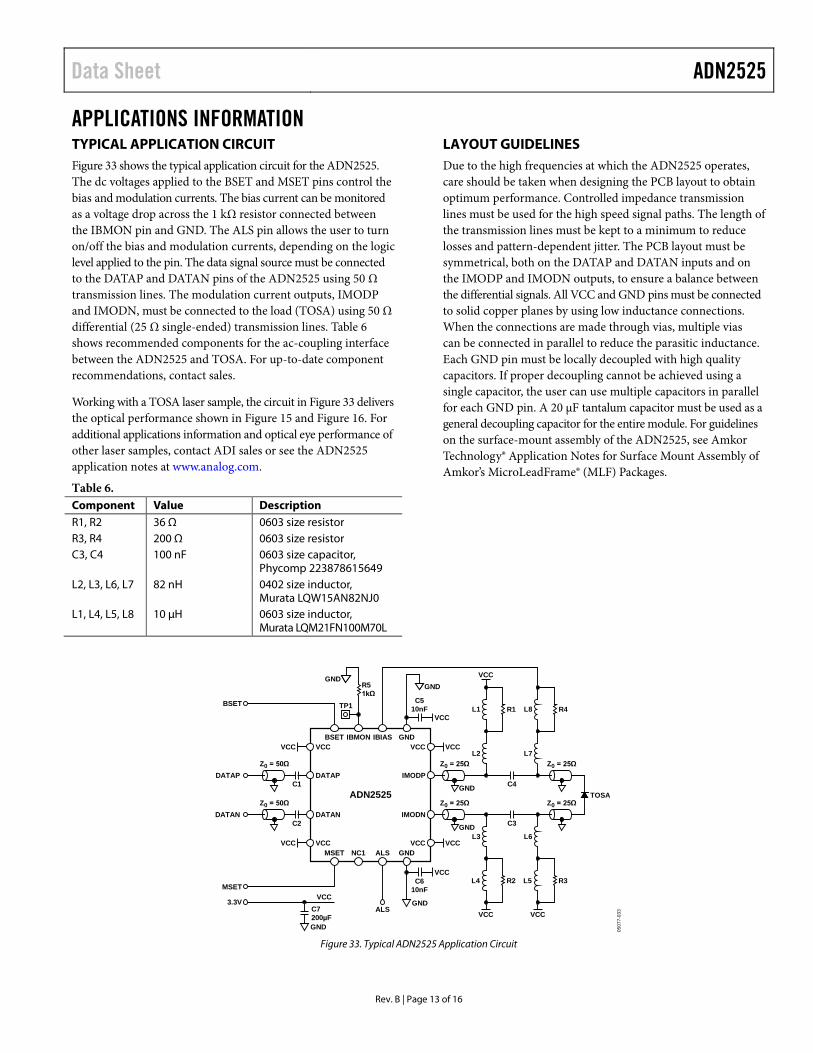
APPLICATIONS INFORMATION TYPICAL APPLICATION CIRCUIT Figure 33 shows the typical application circuit for the ADN2525. The dc voltages applied to the BSET and MSET pins control the bias and modulation currents. The bias current can be monitored as a voltage drop across the 1 kΩ resistor connected between the IBMON pin and GND. The ALS pin allows the user to turn on/off the bias and modulation currents, depending on the logic level applied to the pin. The data signal source must be connected to the DATAP and DATAN pins of the ADN2525 using 50 Ω transmission lines. The modulation current outputs, IMODP and IMODN, must be connected to the load (TOSA) using 50 Ω differential (25 Ω single-ended) transmission lines. Table 6 shows recommended components for the ac-coupling interface between the ADN2525 and TOSA. For up-to-date component recommendations, contact sales.
Working with a TOSA laser sample, the circuit in Figure 33 delivers the optical performance shown in Figure 15 and Figure 16. For additional applications information and optical eye performance of other laser samples, contact ADI sales or see the ADN2525 application notes at www.analog.com.
Table 6. Component Value Description R1, R2 36 Ω 0603 size resistor R3, R4 200 Ω 0603 size resistor C3, C4 100 nF 0603 size capacitor,
Phycomp 223878615649 L2, L3, L6, L7 82 nH 0402 size inductor,
Murata LQW15AN82NJ0 L1, L4, L5, L8 10 µH 0603 size inductor,
Murata LQM21FN100M70L
LAYOUT GUIDELINES Due to the high frequencies at which the ADN2525 operates, care should be taken when designing the PCB layout to obtain optimum performance. Controlled impedance transmission lines must be used for the high speed signal paths. The length of the transmission lines must be kept to a minimum to reduce losses and pattern-dependent jitter. The PCB layout must be symmetrical, both on the DATAP and DATAN inputs and on the IMODP and IMODN outputs, to ensure a balance between the differential signals. All VCC and GND pins must be connected to solid copper planes by using low inductance connections. When the connections are made through vias, multiple vias can be connected in parallel to reduce the parasitic inductance. Each GND pin must be locally decoupled with high quality capacitors. If proper decoupling cannot be achieved using a single capacitor, the user can use multiple capacitors in parallel for each GND pin. A 20 µF tantalum capacitor must be used as a general decoupling capacitor for the entire module. For guidelines on the surface-mount assembly of the ADN2525, see Amkor Technology® Application Notes for Surface Mount Assembly of Amkor’s MicroLeadFrame® (MLF) Packages.
MSET NC1 ALS GND
BSET IBMON IBIAS GNDVCC
DATAP
DATAN
VCC
VCC
IMODP
IMODN
VCC
DATAP
DATAN
C1
C2
MSET
BSET
R51kΩ
ADN2525
Z0 = 50Ω Z0 = 25Ω Z0 = 25Ω
Z0 = 50Ω
GND
VCC
GND
VCC
TOSAC4
C7200µF
L2
L1 R1
3.3V
VCC VCC
VCC
VCC
VCC
TP1C5
10nF
GND
GND
VCCC6
10nF
GNDALS
L7
L8 R4
L6
L5 R3
VCC
L3
L4 R2
VCC
Z0 = 25Ω Z0 = 25Ω
C3GND
0507
7-03
3
Figure 33. Typical ADN2525 Application Circuit
ADN2525 Data Sheet
Rev. B | Page 14 of 16
DESIGN EXAMPLE This design example covers:
• Headroom calculations for IBIAS, IMODP, and IMODN pins.
• Calculation of the typical voltage required at the BSET and MSET pins to produce the desired bias and modulation currents.
This design example assumes that the resistance of the TOSA is 25 Ω, the forward voltage of the laser at low current is VF = 1 V, IBIAS = 40 mA, IMOD = 60 mA, and VCC = 3.3 V.
Headroom Calculations
To ensure proper device operation, the voltages on the IBIAS, IMODP, and IMODN pins must meet the compliance voltage specifications in Table 1.
Considering the typical application circuit shown in Figure 33, the voltage at the IBIAS pin can be written as
VIBIAS = VCC − VF − (IBIAS × RTOSA) − VLA
where:
VCC is the supply voltage.
VF is the forward voltage across the laser at low current.
RTOSA is the resistance of the TOSA.
VLA is the dc voltage drop across L5, L6, L7, and L8.
VLB is the dc voltage drop across L1, L2, L3, and L4.
For proper operation, the minimum voltage at the IBIAS pin should be greater than 0.6 V, as specified by the minimum IBIAS compliance specification in Table 1.
Assuming that the voltage drop across the 25 Ω transmission lines is negligible and that VLA = 0 V, VF = 1 V, and IBIAS = 40 mA,
VIBIAS = 3.3 − 1 − (0.04 × 25) = 1.3 V
VIBIAS = 1.3 V > 0.6 V, which satisfies the requirement
The maximum voltage at the IBIAS pin must be less than the maximum IBIAS compliance specification as described by
VCOMPLIANCE_MAX = VCC − 0.75 − 4.4 × IBIAS (A)
For this example: VCOMPLIANCE_MAX = VCC – 0.75 − 4.4 × 0.04 = 2.53 V
VIBIAS = 1.3 V < 2.53 V, which satisfies the requirement
To calculate the headroom at the modulation current pins (IMODP and IMODN), the voltage has a dc component equal to VCC due to the ac-coupled configuration and a swing equal to IMOD × 25 Ω. For proper operation of the ADN2525, the
voltage at each modulation output pin should be within the normal operation region shown in Figure 30.
Assuming VLB = 0 V and IMOD = 60 mA, the minimum voltage at the modulation output pins is equal to
VCC − (IMOD × 25)/2 = VCC − 0.75
VCC − 0.75 > VCC − 1.1 V, which satisfies the requirement
The maximum voltage at the modulation output pins is equal to
VCC + (IMOD × 25)/2 = VCC + 0.75
VCC + 0.75 < VCC + 1.1 V, which satisfies the requirement
Headroom calculations must be repeated for the minimum and maximum values of the required IBIAS and IMOD ranges to ensure proper device operation over all operating conditions.
BSET and MSET Pin Voltage Calculation
To set the desired bias and modulation currents, the BSET and MSET pins of the ADN2525 must be driven with the appropriate dc voltage. The voltage range required at the BSET pin to generate the required IBIAS range can be calculated using the BSET voltage to IBIAS gain specified in Table 1. Assuming that IBIAS = 40 mA and the typical IBIAS/VBSET ratio of 100 mA/V, the BSET voltage is given by
V4.010040
mA/V100(mA)
===IBIAS
VBSET
The BSET voltage range can be calculated using the required IBIAS range and the minimum and maximum BSET voltage to IBIAS gain values specified in Table 1.
The voltage required at the MSET pin to produce the desired modulation current can be calculated using
KIMODVMSET =
where K is the MSET voltage to IMOD ratio.
The value of K depends on the actual resistance of the TOSA. It can be read using the plot shown in Figure 29. For a TOSA resistance of 25 Ω, the typical value of K = 120 mA/V. Assuming that IMOD = 60 mA and using the preceding equation, the MSET voltage is given by
V5.012060
mA/V120(mA)
===IMOD
VMSET
The MSET voltage range can be calculated using the required IMOD range and the minimum and maximum K values. These can be obtained from the minimum and maximum curves in Figure 29.

Data Sheet ADN2525
Rev. B | Page 15 of 16
OUTLINE DIMENSIONS
0.300.230.18
1.751.60 SQ1.45
3.103.00 SQ2.90
10.50BSC
BOTTOM VIEWTOP VIEW
16
58
9
12
13
4
0.500.400.30
0.05 MAX0.02 NOM
0.20 REF
0.20 MIN
COPLANARITY0.08
PIN 1INDICATOR
0.800.750.70
COMPLIANT TOJEDEC STANDARDS MO-220-WEED-6.PK
G-0
05
13
8
SEATINGPLANE
TOP VIEW
EXPOSEDPAD
02-2
3-2
017
-E
PIN 1INDICATOR AREA OPTIONS(SEE DETAIL A)
DETAIL A(JEDEC 95)
FOR PROPER CONNECTION OFTHE EXPOSED PAD, REFER TOTHE PIN CONFIGURATION ANDFUNCTION DESCRIPTIONSSECTION OF THIS DATA SHEET.
Figure 34. 16-Lead Lead Frame Chip Scale Package [LFCSP]
3 mm × 3 mm Body and 0.75 mm Package Height (CP-16-22)
Dimensions shown in millimeters
ORDERING GUIDE Model1 Temperature Range Package Description Package Option Branding ADN2525ACPZ-R2 −40°C to +85°C 16-Lead LFCSP, 250-Piece Reel CP-16-22 F06 ADN2525ACPZ-500R7 −40°C to +85°C 16-Lead LFCSP, 7” 1,500-Piece Reel CP-16-22 F06 ADN2525ACPZ-REEL7 −40°C to +85°C 16-Lead LFCSP, 7” 500-Piece Reel CP-16-22 F06 1 Z = RoHS Compliant part.

ADN2525 Data Sheet
Rev. B | Page 16 of 16
NOTES
©2005–2017 Analog Devices, Inc. All rights reserved. Trademarks and registered trademarks are the property of their respective owners. D05077-0-4/17(B)