Embed Size (px)
Citation preview
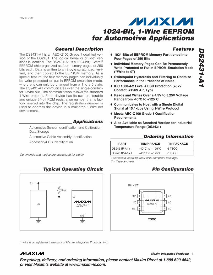
General DescriptionThe DS2431-A1 is an AEC-Q100 Grade 1 qualified ver-sion of the DS2431. The logical behavior of both ver-sions is identical. The DS2431-A1 is a 1024-bit, 1-Wire®
EEPROM chip organized as four memory pages of 256bits each. Data is written to an 8-byte scratchpad, veri-fied, and then copied to the EEPROM memory. As aspecial feature, the four memory pages can individuallybe write protected or put in EPROM-emulation mode,where bits can only be changed from a 1 to a 0 state.The DS2431-A1 communicates over the single-conduc-tor 1-Wire bus. The communication follows the standard1-Wire protocol. Each device has its own unalterableand unique 64-bit ROM registration number that is fac-tory lasered into the chip. The registration number isused to address the device in a multidrop 1-Wire netenvironment.
ApplicationsAutomotive Sensor Identification and CalibrationData Storage
Automotive Cable Assembly Identification
Accessory/PCB Identification
Features♦ 1024 Bits of EEPROM Memory Partitioned Into
Four Pages of 256 Bits
♦ Individual Memory Pages Can Be PermanentlyWrite Protected or Put in EPROM-Emulation Mode(“Write to 0”)
♦ Switchpoint Hysteresis and Filtering to OptimizePerformance in the Presence of Noise
♦ IEC 1000-4-2 Level 4 ESD Protection (+8kVContact, +15kV Air, Typ)
♦ Reads and Writes Over a 4.5V to 5.25V VoltageRange from -40°C to +125°C
♦ Communicates to Host with a Single DigitalSignal at 15.4kbps Using 1-Wire Protocol
♦ Meets AEC-Q100 Grade 1 QualificationRequirements
♦ Also Available as Standard Version for IndustrialTemperature Range (DS2431)
DS
24
31
-A1
1024-Bit, 1-Wire EEPROMfor Automotive Applications
________________________________________________________________ Maxim Integrated Products 1
N.C.
I/O
GND
N.C.
N.C.
N.C.
TSOC
TOP VIEW
+
5
4
6
2
3
1
DS2431-A1
Pin Configuration
Ordering Information
DS2431-A1
I/O
RPUP
VCC
μC
GND
Typical Operating Circuit
Rev 1; 3/08
For pricing, delivery, and ordering information, please contact Maxim Direct at 1-888-629-4642,or visit Maxim’s website at www.maxim-ic.com.
+Denotes a lead(Pb)-free/RoHS-compliant package.T = Tape and reel.
PART TEMP RANGE PIN-PACKAGE
DS2431P-A1+ -40°C to +125°C 6 TSOC
DS2431P-A1+T -40°C to +125°C 6 TSOC Commands and modes are capitalized for clarity.
1-Wire is a registered trademark of Maxim Integrated Products, Inc.
DS
24
31
-A1
1024-Bit, 1-Wire EEPROMfor Automotive Applications
2 _______________________________________________________________________________________
ABSOLUTE MAXIMUM RATINGS
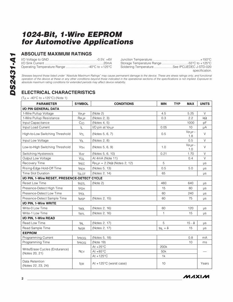
ELECTRICAL CHARACTERISTICS(TA = -40°C to +125°C) (Note 1)
Stresses beyond those listed under “Absolute Maximum Ratings” may cause permanent damage to the device. These are stress ratings only, and functionaloperation of the device at these or any other conditions beyond those indicated in the operational sections of the specifications is not implied. Exposure toabsolute maximum rating conditions for extended periods may affect device reliability.
I/O Voltage to GND .....................................................-0.5V, +6VI/O Sink Current ..................................................................20mAOperating Temperature Range .........................-40°C to +125°C
Junction Temperature ......................................................+150°CStorage Temperature Range .............................-55°C to +125°CSoldering Temperature .....................See IPC/JEDEC J-STD-020
specification.
PARAMETER SYMBOL CONDITIONS MIN TYP MAX UNITS
I/O PIN GENERAL DATA1-Wire Pullup Voltage VPUP (Note 2) 4.5 5.25 V 1-Wire Pullup Resistance RPUP (Notes 2, 3) 0.3 2.2 kInput Capacitance CIO (Notes 4, 5) 1000 pF Input Load Current IL I/O pin at VPUP 0.05 10 μA
High-to-Low Switching Threshold VTL (Notes 5, 6, 7) 0.5 VPUP -
1.8 V
Input Low Voltage VIL (Notes 2, 8) 0.5 V
Low-to-High Switching Threshold VTH (Notes 5, 6, 9) 1.0 VPUP -
1.0 V
Switching Hysteresis VHY (Notes 5, 6, 10) 0.21 1.70 V Output Low Voltage VOL At 4mA (Note 11) 0.4 V
Recovery Time tREC RPUP = 2.2k (Notes 2, 12) 5 μs
Rising-Edge Hold-Off Time tREH (Notes 5, 13) 0.5 5.0 μs
Time Slot Duration tSLOT (Notes 2, 14) 65 μs
I/O PIN, 1-Wire RESET, PRESENCE-DETECT CYCLE
Reset Low Time tRSTL (Note 2) 480 640 μs
Presence-Detect High Time tPDH 15 60 μs
Presence-Detect Low Time tPDL 60 240 μs
Presence-Detect Sample Time tMSP (Notes 2, 15) 60 75 μs
I/O PIN, 1-Wire WRITE
Write-0 Low Time tW0L (Notes 2, 16) 60 120 μs
Write-1 Low Time tW1L (Notes 2, 16) 1 15 μs
I/O PIN, 1-Wire READ
Read Low Time tRL (Notes 2, 17) 5 15 - μs
Read Sample Time tMSR (Notes 2, 17) tRL + 15 μs
EEPROMProgramming Current IPROG (Notes 5, 18) 0.8 mA Programming Time tPROG (Note 19) 10 ms
At +25°C 200k At +85°C 50k
Write/Erase Cycles (Endurance) (Notes 20, 21)
NCY
At +125°C 1k
Data Retention (Notes 22, 23, 24)
tDR At +125°C (worst case) 10 Years
DS
24
31
-A1
1024-Bit, 1-Wire EEPROMfor Automotive Applications
_______________________________________________________________________________________ 3
Note 1: Specifications at TA = -40°C are guaranteed by design only and not production tested.Note 2: System requirement.Note 3: Maximum allowable pullup resistance is a function of the number of 1-Wire devices in the system and 1-Wire recovery times.
The specified value here applies to systems with only one device and with the minimum 1-Wire recovery times. For moreheavily loaded systems, an active pullup such as that found in the DS2482-x00, DS2480B, or DS2490 may be required.
Note 4: Maximum value represents the internal parasite capacitance when VPUP is first applied. If a 2.2kΩ resistor is used to pullup the data line, 2.5µs after VPUP has been applied, the parasite capacitance does not affect normal communications.
Note 5: Guaranteed by design, characterization, and/or simulation only. Not production tested.Note 6: VTL, VTH, and VHY are a function of the internal supply voltage, which is a function of VPUP, RPUP, 1-Wire timing, and
capacitive loading on I/O. Lower VPUP, higher RPUP, shorter tREC, and heavier capacitive loading all lead to lower valuesof VTL, VTH, and VHY.
Note 7: Voltage below which, during a falling edge on I/O, a logic 0 is detected.Note 8: The voltage on I/O needs to be less than or equal to VILMAX at all times the master is driving I/O to a logic-0 level.Note 9: Voltage above which, during a rising edge on I/O, a logic 1 is detected.Note 10: After VTH is crossed during a rising edge on I/O, the voltage on I/O must drop by at least VHY to be detected as logic 0.Note 11: The I-V characteristic is linear for voltages less than 1V.Note 12: Applies to a single device attached to a 1-Wire line.Note 13: The earliest recognition of a negative edge is possible at tREH after VTH has been reached on the preceding rising edge.Note 14: Defines maximum possible bit rate. Equal to tW0LMIN + tRECMIN.Note 15: Interval after tRSTL during which a bus master is guaranteed to sample a logic 0 on I/O if there is a DS2431-A1 present.
Minimum limit is tPDHMAX; maximum limit is tPDHMIN + tPDLMIN.Note 16: ε in Figure 11 represents the time required for the pullup circuitry to pull the voltage on I/O up from VIL to VTH. The actual
maximum duration for the master to pull the line low is tW1LMAX + tF - ε and tW0LMAX + tF - ε, respectively.Note 17: δ in Figure 11 represents the time required for the pullup circuitry to pull the voltage on I/O up from VIL to the input-high
threshold of the bus master. The actual maximum duration for the master to pull the line low is tRLMAX + tF.Note 18: Current drawn from I/O during the EEPROM programming interval. The pullup circuit on I/O during the programming inter-
val should be such that the voltage at I/O is greater than or equal to VPUPMIN. If VPUP in the system is close to VPUPMIN, alow-impedance bypass of RPUP, which can be activated during programming, may need to be added.
Note 19: Interval begins tREHMAX after the trailing rising edge on I/O for the last time slot of the E/S byte for a valid CopyScratchpad sequence. Interval ends once the device’s self-timed EEPROM programming cycle is complete and the cur-rent drawn by the device has returned from IPROG to IL.
Note 20: Write-cycle endurance is degraded as TA increases.Note 21: Not 100% production tested; guaranteed by reliability monitor sampling.Note 22: Data retention is degraded as TA increases.Note 23: Guaranteed by 100% production test at elevated temperature for a shorter time; equivalence of this production test to the
data sheet limit at operating temperature range is established by reliability testing.Note 24: EEPROM writes can become nonfunctional after the data-retention time is exceeded. Long-term storage at elevated tem-
peratures is not recommended; the device can lose its write capability after 10 years at +125°C or 40 years at +85°C.
DS
24
31
-A1
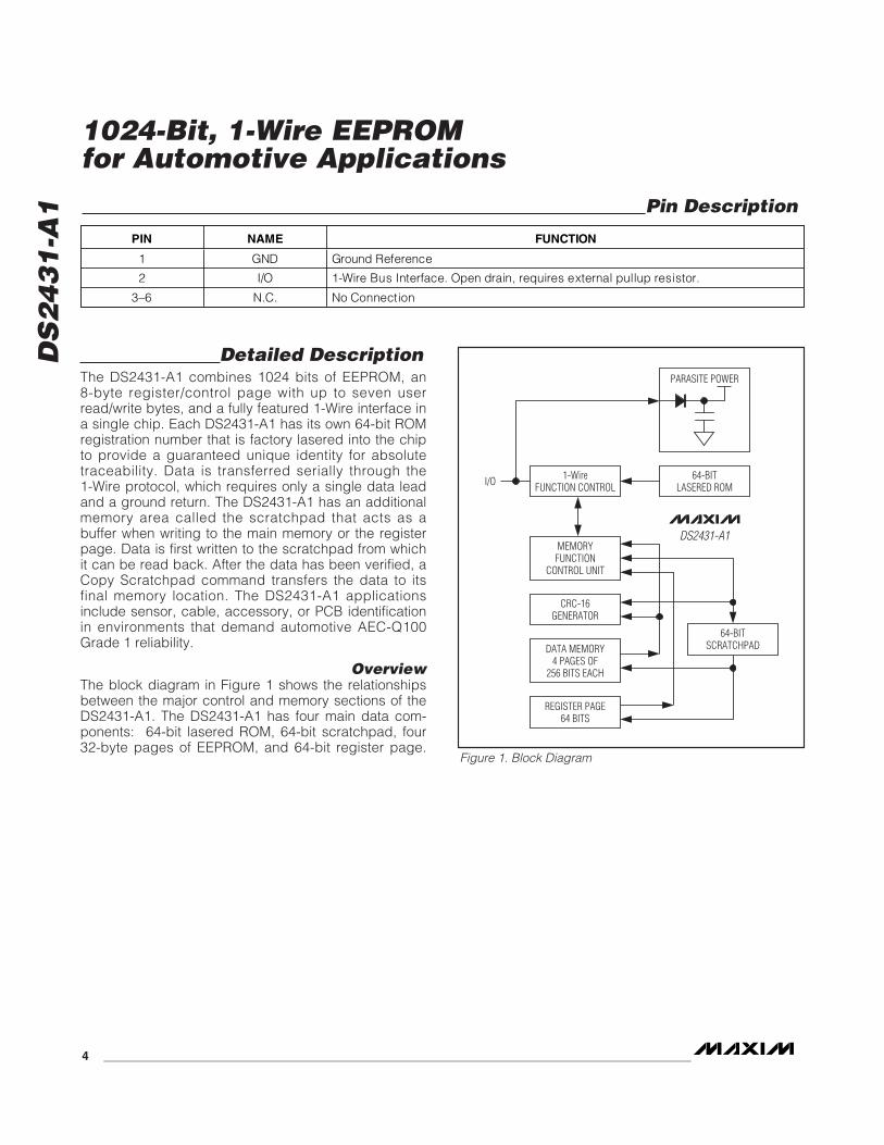
Detailed DescriptionThe DS2431-A1 combines 1024 bits of EEPROM, an 8-byte register/control page with up to seven userread/write bytes, and a fully featured 1-Wire interface ina single chip. Each DS2431-A1 has its own 64-bit ROMregistration number that is factory lasered into the chipto provide a guaranteed unique identity for absolutetraceability. Data is transferred serially through the 1-Wire protocol, which requires only a single data leadand a ground return. The DS2431-A1 has an additionalmemory area called the scratchpad that acts as abuffer when writing to the main memory or the registerpage. Data is first written to the scratchpad from whichit can be read back. After the data has been verified, aCopy Scratchpad command transfers the data to itsfinal memory location. The DS2431-A1 applicationsinclude sensor, cable, accessory, or PCB identificationin environments that demand automotive AEC-Q100Grade 1 reliability.
OverviewThe block diagram in Figure 1 shows the relationshipsbetween the major control and memory sections of theDS2431-A1. The DS2431-A1 has four main data com-ponents: 64-bit lasered ROM, 64-bit scratchpad, four32-byte pages of EEPROM, and 64-bit register page.
1024-Bit, 1-Wire EEPROMfor Automotive Applications
4 _______________________________________________________________________________________
Pin Description
PIN NAME FUNCTION
1 GND Ground Reference
2 I/O 1-Wire Bus Interface. Open drain, requires external pullup resistor.
3–6 N.C. No Connection
DS2431-A1MEMORY
FUNCTIONCONTROL UNIT
DATA MEMORY4 PAGES OF
256 BITS EACH
CRC-16GENERATOR
64-BITSCRATCHPAD
1-WireFUNCTION CONTROL
64-BITLASERED ROM
PARASITE POWER
I/O
REGISTER PAGE64 BITS
Figure 1. Block Diagram
The hierarchical structure of the 1-Wire protocol isshown in Figure 2. The bus master must first provideone of the five ROM function commands: Read ROM,Match ROM, Search ROM, Skip ROM, and Resume.The protocol required for these ROM function com-mands is described in Figure 9. After a ROM functioncommand is successfully executed, the memory func-tions become accessible and the master can provideany one of the four memory function commands. Theprotocol for these memory function commands isdescribed in Figure 7. All data is read and writtenleast significant bit first.
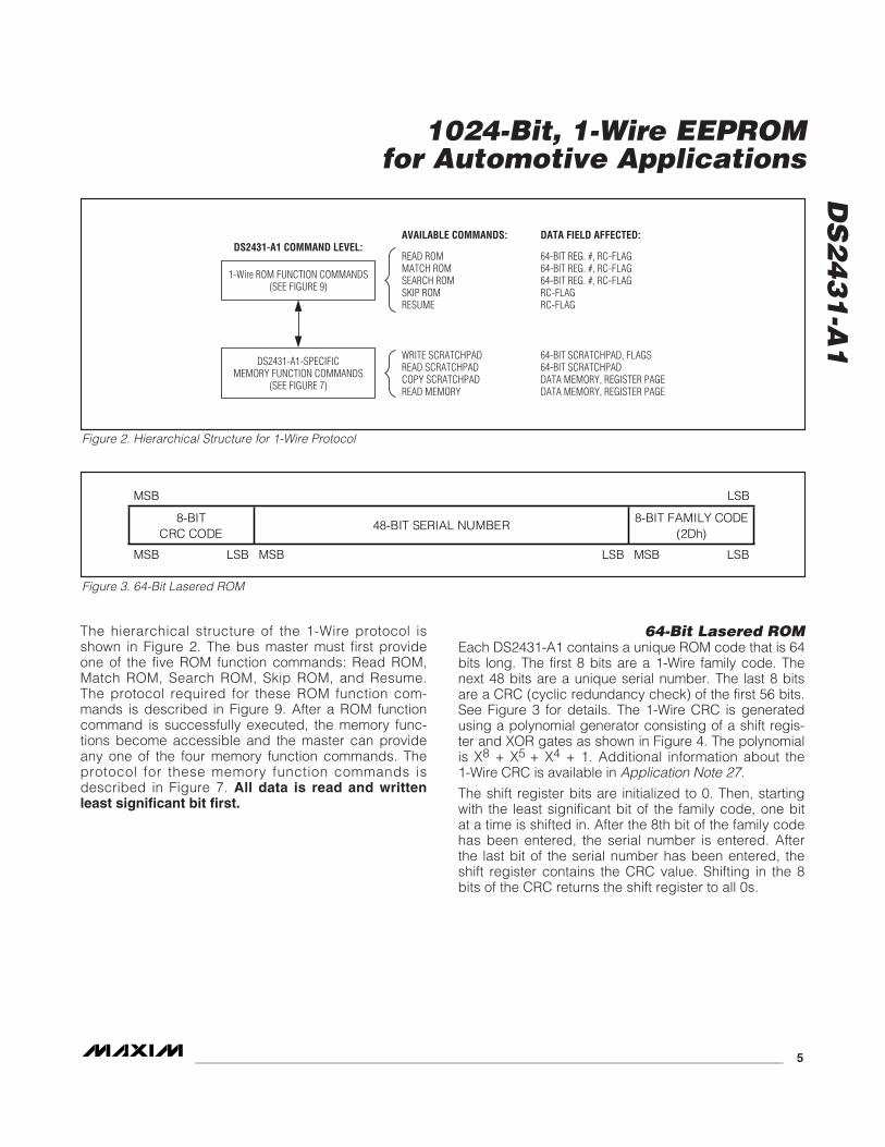
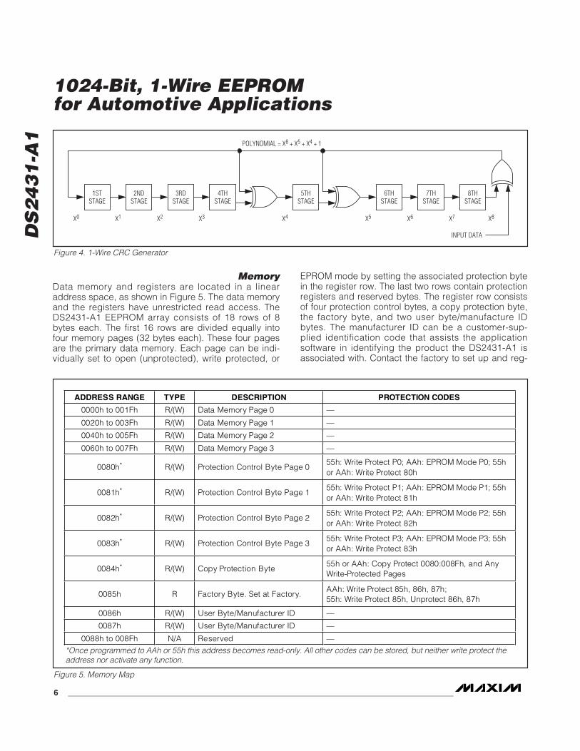
64-Bit Lasered ROMEach DS2431-A1 contains a unique ROM code that is 64bits long. The first 8 bits are a 1-Wire family code. Thenext 48 bits are a unique serial number. The last 8 bitsare a CRC (cyclic redundancy check) of the first 56 bits.See Figure 3 for details. The 1-Wire CRC is generatedusing a polynomial generator consisting of a shift regis-ter and XOR gates as shown in Figure 4. The polynomialis X8 + X5 + X4 + 1. Additional information about the 1-Wire CRC is available in Application Note 27.
The shift register bits are initialized to 0. Then, startingwith the least significant bit of the family code, one bitat a time is shifted in. After the 8th bit of the family codehas been entered, the serial number is entered. Afterthe last bit of the serial number has been entered, theshift register contains the CRC value. Shifting in the 8bits of the CRC returns the shift register to all 0s.
DS
24
31
-A1
1024-Bit, 1-Wire EEPROMfor Automotive Applications
_______________________________________________________________________________________ 5
DS2431-A1 COMMAND LEVEL:AVAILABLE COMMANDS: DATA FIELD AFFECTED:
READ ROMMATCH ROMSEARCH ROMSKIP ROMRESUME
64-BIT REG. #, RC-FLAG64-BIT REG. #, RC-FLAG64-BIT REG. #, RC-FLAGRC-FLAGRC-FLAG
1-Wire ROM FUNCTION COMMANDS(SEE FIGURE 9)
WRITE SCRATCHPADREAD SCRATCHPADCOPY SCRATCHPADREAD MEMORY
64-BIT SCRATCHPAD, FLAGS64-BIT SCRATCHPADDATA MEMORY, REGISTER PAGEDATA MEMORY, REGISTER PAGE
DS2431-A1-SPECIFICMEMORY FUNCTION COMMANDS
(SEE FIGURE 7)
Figure 2. Hierarchical Structure for 1-Wire Protocol
MSB LSB
8-BIT CRC CODE
48-BIT SERIAL NUMBER 8-BIT FAMILY CODE
(2Dh)
MSB LSB MSB LSB MSB LSB
Figure 3. 64-Bit Lasered ROM
DS
24
31
-A1
MemoryData memory and registers are located in a linearaddress space, as shown in Figure 5. The data memoryand the registers have unrestricted read access. TheDS2431-A1 EEPROM array consists of 18 rows of 8bytes each. The first 16 rows are divided equally intofour memory pages (32 bytes each). These four pagesare the primary data memory. Each page can be indi-vidually set to open (unprotected), write protected, or
EPROM mode by setting the associated protection bytein the register row. The last two rows contain protectionregisters and reserved bytes. The register row consistsof four protection control bytes, a copy protection byte,the factory byte, and two user byte/manufacture IDbytes. The manufacturer ID can be a customer-sup-plied identification code that assists the applicationsoftware in identifying the product the DS2431-A1 isassociated with. Contact the factory to set up and reg-
1024-Bit, 1-Wire EEPROMfor Automotive Applications
6 _______________________________________________________________________________________
1STSTAGE
2NDSTAGE
3RDSTAGE
4THSTAGE
7THSTAGE
8THSTAGE
6THSTAGE
5THSTAGE
X0 X1 X2 X3 X4
POLYNOMIAL = X8 + X5 + X4 + 1
INPUT DATA
X5 X6 X7 X8
Figure 4. 1-Wire CRC Generator
ADDRESS RANGE TYPE DESCRIPTION PROTECTION CODES
0000h to 001Fh R/(W) Data Memory Page 0 —
0020h to 003Fh R/(W) Data Memory Page 1 —
0040h to 005Fh R/(W) Data Memory Page 2 —
0060h to 007Fh R/(W) Data Memory Page 3 —
0080h* R/(W) Protection Control Byte Page 0 55h: Write Protect P0; AAh: EPROM Mode P0; 55h or AAh: Write Protect 80h
0081h* R/(W) Protection Control Byte Page 1 55h: Write Protect P1; AAh: EPROM Mode P1; 55h or AAh: Write Protect 81h
0082h* R/(W) Protection Control Byte Page 2 55h: Write Protect P2; AAh: EPROM Mode P2; 55h or AAh: Write Protect 82h
0083h* R/(W) Protection Control Byte Page 3 55h: Write Protect P3; AAh: EPROM Mode P3; 55h or AAh: Write Protect 83h
0084h* R/(W) Copy Protection Byte 55h or AAh: Copy Protect 0080:008Fh, and Any Write-Protected Pages
0085h R Factory Byte. Set at Factory. AAh: Write Protect 85h, 86h, 87h; 55h: Write Protect 85h, Unprotect 86h, 87h
0086h R/(W) User Byte/Manufacturer ID —
0087h R/(W) User Byte/Manufacturer ID —
0088h to 008Fh N/A Reserved —
Figure 5. Memory Map
*Once programmed to AAh or 55h this address becomes read-only. All other codes can be stored, but neither write protect theaddress nor activate any function.
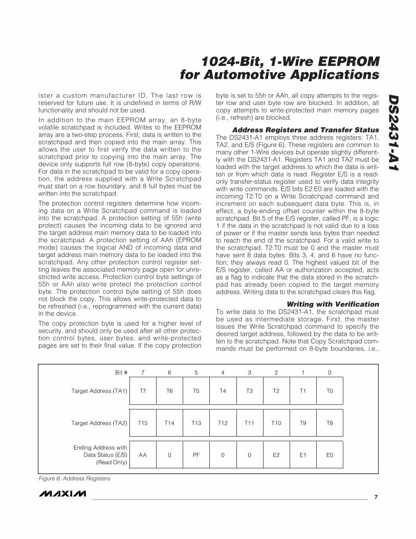
ister a custom manufacturer ID. The last row isreserved for future use. It is undefined in terms of R/Wfunctionality and should not be used.
In addition to the main EEPROM array, an 8-bytevolatile scratchpad is included. Writes to the EEPROMarray are a two-step process. First, data is written to thescratchpad and then copied into the main array. Thisallows the user to first verify the data written to thescratchpad prior to copying into the main array. Thedevice only supports full row (8-byte) copy operations.For data in the scratchpad to be valid for a copy opera-tion, the address supplied with a Write Scratchpadmust start on a row boundary, and 8 full bytes must bewritten into the scratchpad.
The protection control registers determine how incom-ing data on a Write Scratchpad command is loadedinto the scratchpad. A protection setting of 55h (writeprotect) causes the incoming data to be ignored andthe target address main memory data to be loaded intothe scratchpad. A protection setting of AAh (EPROMmode) causes the logical AND of incoming data andtarget address main memory data to be loaded into thescratchpad. Any other protection control register set-ting leaves the associated memory page open for unre-stricted write access. Protection control byte settings of55h or AAh also write protect the protection controlbyte. The protection control byte setting of 55h doesnot block the copy. This allows write-protected data tobe refreshed (i.e., reprogrammed with the current data)in the device.
The copy protection byte is used for a higher level ofsecurity, and should only be used after all other protec-tion control bytes, user bytes, and write-protectedpages are set to their final value. If the copy protection
byte is set to 55h or AAh, all copy attempts to the regis-ter row and user byte row are blocked. In addition, allcopy attempts to write-protected main memory pages(i.e., refresh) are blocked.
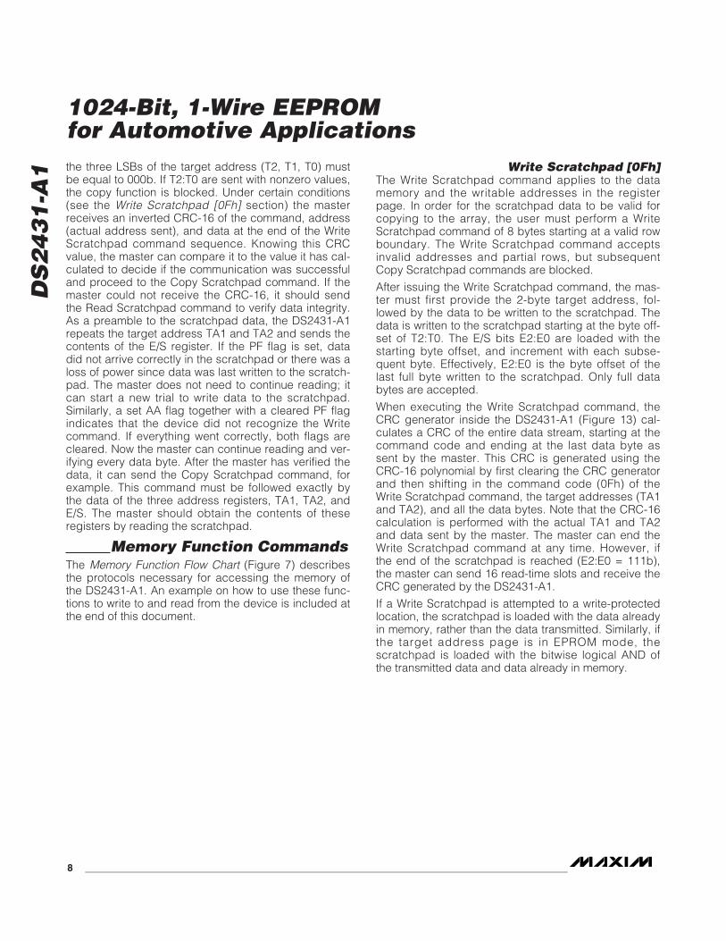
Address Registers and Transfer StatusThe DS2431-A1 employs three address registers: TA1,TA2, and E/S (Figure 6). These registers are common tomany other 1-Wire devices but operate slightly different-ly with the DS2431-A1. Registers TA1 and TA2 must beloaded with the target address to which the data is writ-ten or from which data is read. Register E/S is a read-only transfer-status register used to verify data integritywith write commands. E/S bits E2:E0 are loaded with theincoming T2:T0 on a Write Scratchpad command andincrement on each subsequent data byte. This is, ineffect, a byte-ending offset counter within the 8-bytescratchpad. Bit 5 of the E/S register, called PF, is a logic1 if the data in the scratchpad is not valid due to a lossof power or if the master sends less bytes than neededto reach the end of the scratchpad. For a valid write tothe scratchpad, T2:T0 must be 0 and the master musthave sent 8 data bytes. Bits 3, 4, and 6 have no func-tion; they always read 0. The highest valued bit of theE/S register, called AA or authorization accepted, actsas a flag to indicate that the data stored in the scratch-pad has already been copied to the target memoryaddress. Writing data to the scratchpad clears this flag.
Writing with VerificationTo write data to the DS2431-A1, the scratchpad mustbe used as intermediate storage. First, the masterissues the Write Scratchpad command to specify thedesired target address, followed by the data to be writ-ten to the scratchpad. Note that Copy Scratchpad com-mands must be performed on 8-byte boundaries, i.e.,
DS
24
31
-A1
1024-Bit, 1-Wire EEPROMfor Automotive Applications
_______________________________________________________________________________________ 7
Bit # 7 6 5 4 3 2 1 0
Target Address (TA1) T7 T6 T5 T4 T3 T2 T1 T0
Target Address (TA2) T15 T14 T13 T12 T11 T10 T9 T8
Ending Address with Data Status (E/S)
(Read Only) AA 0 PF 0 0 E2 E1 E0
Figure 6. Address Registers
DS
24
31
-A1 the three LSBs of the target address (T2, T1, T0) must
be equal to 000b. If T2:T0 are sent with nonzero values,the copy function is blocked. Under certain conditions(see the Write Scratchpad [0Fh] section) the masterreceives an inverted CRC-16 of the command, address(actual address sent), and data at the end of the WriteScratchpad command sequence. Knowing this CRCvalue, the master can compare it to the value it has cal-culated to decide if the communication was successfuland proceed to the Copy Scratchpad command. If themaster could not receive the CRC-16, it should sendthe Read Scratchpad command to verify data integrity.As a preamble to the scratchpad data, the DS2431-A1repeats the target address TA1 and TA2 and sends thecontents of the E/S register. If the PF flag is set, datadid not arrive correctly in the scratchpad or there was aloss of power since data was last written to the scratch-pad. The master does not need to continue reading; itcan start a new trial to write data to the scratchpad.Similarly, a set AA flag together with a cleared PF flagindicates that the device did not recognize the Writecommand. If everything went correctly, both flags arecleared. Now the master can continue reading and ver-ifying every data byte. After the master has verified thedata, it can send the Copy Scratchpad command, forexample. This command must be followed exactly bythe data of the three address registers, TA1, TA2, andE/S. The master should obtain the contents of theseregisters by reading the scratchpad.
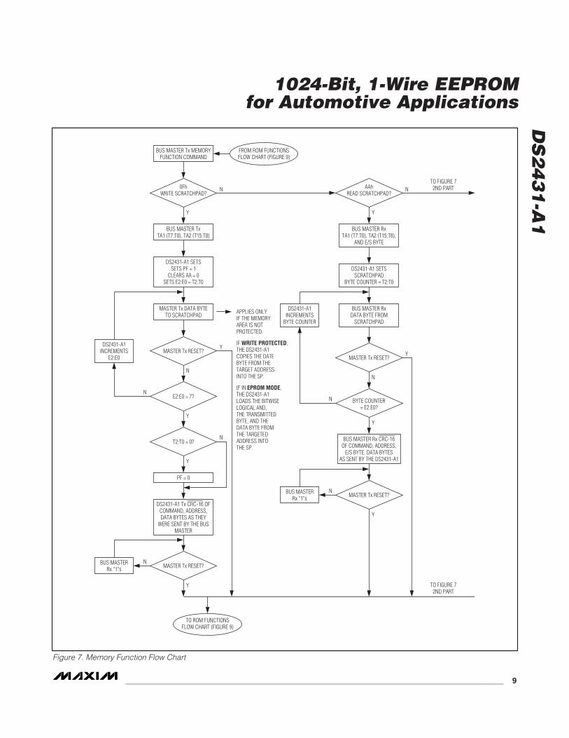
Memory Function CommandsThe Memory Function Flow Chart (Figure 7) describesthe protocols necessary for accessing the memory ofthe DS2431-A1. An example on how to use these func-tions to write to and read from the device is included atthe end of this document.
Write Scratchpad [0Fh]The Write Scratchpad command applies to the datamemory and the writable addresses in the registerpage. In order for the scratchpad data to be valid forcopying to the array, the user must perform a WriteScratchpad command of 8 bytes starting at a valid rowboundary. The Write Scratchpad command acceptsinvalid addresses and partial rows, but subsequentCopy Scratchpad commands are blocked.
After issuing the Write Scratchpad command, the mas-ter must first provide the 2-byte target address, fol-lowed by the data to be written to the scratchpad. Thedata is written to the scratchpad starting at the byte off-set of T2:T0. The E/S bits E2:E0 are loaded with thestarting byte offset, and increment with each subse-quent byte. Effectively, E2:E0 is the byte offset of thelast full byte written to the scratchpad. Only full databytes are accepted.
When executing the Write Scratchpad command, theCRC generator inside the DS2431-A1 (Figure 13) cal-culates a CRC of the entire data stream, starting at thecommand code and ending at the last data byte assent by the master. This CRC is generated using theCRC-16 polynomial by first clearing the CRC generatorand then shifting in the command code (0Fh) of theWrite Scratchpad command, the target addresses (TA1and TA2), and all the data bytes. Note that the CRC-16calculation is performed with the actual TA1 and TA2and data sent by the master. The master can end theWrite Scratchpad command at any time. However, ifthe end of the scratchpad is reached (E2:E0 = 111b),the master can send 16 read-time slots and receive theCRC generated by the DS2431-A1.
If a Write Scratchpad is attempted to a write-protectedlocation, the scratchpad is loaded with the data alreadyin memory, rather than the data transmitted. Similarly, ifthe target address page is in EPROM mode, thescratchpad is loaded with the bitwise logical AND ofthe transmitted data and data already in memory.
1024-Bit, 1-Wire EEPROMfor Automotive Applications
8 _______________________________________________________________________________________
DS
24
31
-A1
1024-Bit, 1-Wire EEPROMfor Automotive Applications
_______________________________________________________________________________________ 9
BUS MASTER Tx MEMORYFUNCTION COMMAND
BUS MASTER TxTA1 (T7:T0), TA2 (T15:T8)
BUS MASTER RxTA1 (T7:T0), TA2 (T15:T8),
AND E/S BYTE
BUS MASTER RxDATA BYTE FROM
SCRATCHPAD
MASTER Tx DATA BYTETO SCRATCHPAD APPLIES ONLY
IF THE MEMORYAREA IS NOTPROTECTED.
IF WRITE PROTECTED,THE DS2431-A1COPIES THE DATEBYTE FROM THE TARGET ADDRESSINTO THE SP.
IF IN EPROM MODE,THE DS2431-A1LOADS THE BITWISELOGICAL AND, THE TRANSMITTEDBYTE, AND THEDATA BYTE FROMTHE TARGETEDADDRESS INTOTHE SP.
BUS MASTERRx "1"s
DS2431-A1INCREMENTS
E2:E0
PF = 0
DS2431-A1 SETSSETS PF = 1
CLEARS AA = 0SETS E2:E0 = T2:T0
0FhWRITE SCRATCHPAD?
N
Y
N
Y
N
Y
Y
Y
N
N
MASTER Tx RESET?
E2:E0 = 7?
T2:T0 = 0?
MASTER Tx RESET?
DS2431-A1 SETSSCRATCHPAD
BYTE COUNTER = T2:T0
AAhREAD SCRATCHPAD?
N
Y
DS2431-A1 Tx CRC-16 OFCOMMAND, ADDRESS,DATA BYTES AS THEY
WERE SENT BY THE BUSMASTER
BUS MASTERRx "1"s
Y
NMASTER Tx RESET?
BUS MASTER Rx CRC-16OF COMMAND, ADDRESS,
E/S BYTE, DATA BYTESAS SENT BY THE DS2431-A1
Y
N
MASTER Tx RESET?
Y
BYTE COUNTER= E2:E0?
FROM ROM FUNCTIONSFLOW CHART (FIGURE 9)
TO ROM FUNCTIONSFLOW CHART (FIGURE 9)
DS2431-A1INCREMENTS
BYTE COUNTER
N
TO FIGURE 72ND PART
TO FIGURE 72ND PART
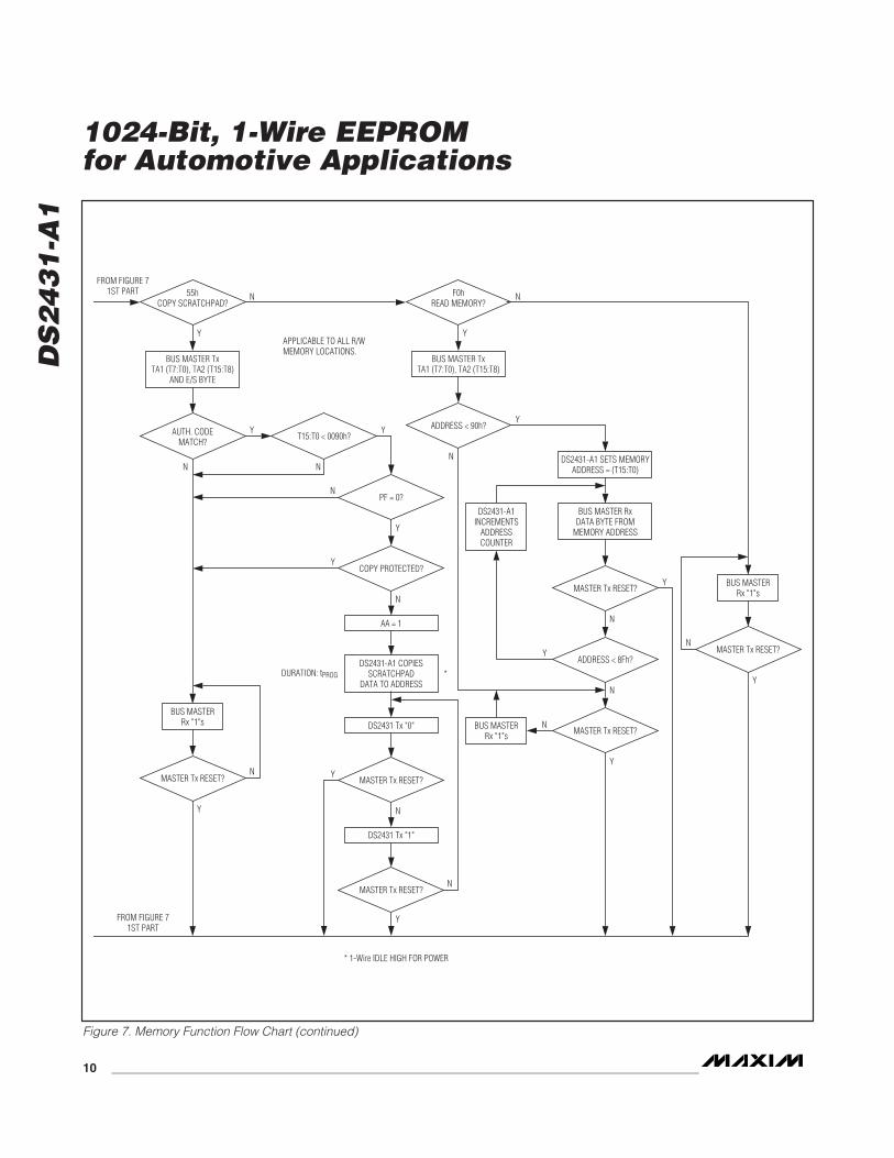
Figure 7. Memory Function Flow Chart
DS
24
31
-A1
1024-Bit, 1-Wire EEPROMfor Automotive Applications
10 ______________________________________________________________________________________
BUS MASTER TxTA1 (T7:T0), TA2 (T15:T8)
APPLICABLE TO ALL R/WMEMORY LOCATIONS.
DURATION: tPROG *
* 1-Wire IDLE HIGH FOR POWER
DS2431-A1 COPIESSCRATCHPAD
DATA TO ADDRESS
BUS MASTERRx "1"s
AA = 1
BUS MASTERRx "1"s
MASTER Tx RESET?N Y
N
N
MASTER Tx RESET?
Y
MASTER Tx RESET?
BUS MASTER TxTA1 (T7:T0), TA2 (T15:T8)
AND E/S BYTE
55hCOPY SCRATCHPAD?
N
Y
Y
Y
N
DS2431 Tx "0"
DS2431 Tx "1"
F0hREAD MEMORY?
N
Y
Y
N
AUTH. CODEMATCH?
Y
N
Y
N
N
T15:T0 < 0090h?
PF = 0?
ADDRESS < 90h?
YCOPY PROTECTED?
BUS MASTERRx "1"s
MASTER Tx RESET?N
Y
DS2431-A1 SETS MEMORYADDRESS = (T15:T0)
BUS MASTER RxDATA BYTE FROM
MEMORY ADDRESS
Y
N
N
MASTER Tx RESET?
ADDRESS < 8Fh?
N
Y
MASTER Tx RESET?
DS2431-A1INCREMENTS
ADDRESSCOUNTER
Y
FROM FIGURE 71ST PART
FROM FIGURE 71ST PART
Figure 7. Memory Function Flow Chart (continued)
Read Scratchpad [AAh]The Read Scratchpad command allows verifying thetarget address and the integrity of the scratchpad data.After issuing the command code, the master beginsreading. The first two bytes are the target address. Thenext byte is the ending offset/data status byte (E/S) fol-lowed by the scratchpad data, which may be differentfrom what the master originally sent. This is of particularimportance if the target address is within the registerpage or a page in either Write Protection or EPROMmodes. See the Write Scratchpad [0Fh] section fordetails. The master should read through the scratchpad(E2:E0 - T2:T0 + 1 bytes), after which it receives theinverted CRC, based on data as it was sent by theDS2431-A1. If the master continues reading after theCRC, all data are logic 1s.
Copy Scratchpad [55h]The Copy Scratchpad command is used to copy datafrom the scratchpad to writable memory sections. Afterissuing the Copy Scratchpad command, the mastermust provide a 3-byte authorization pattern, whichshould have been obtained by an immediately preced-ing Read Scratchpad command. This 3-byte patternmust exactly match the data contained in the threeaddress registers (TA1, TA2, E/S, in that order). If thepattern matches, the target address is valid, the PF flagis not set, and the target memory is not copy protected,then the AA (authorization accepted) flag is set and thecopy begins. All eight bytes of scratchpad contents arecopied to the target memory location. The duration ofthe device’s internal data transfer is tPROG duringwhich the voltage on the 1-Wire bus must not fall below2.8V. A pattern of alternating 0s and 1s are transmittedafter the data has been copied until the master issues areset pulse. If the PF flag is set or the target memory iscopy protected, the copy does not begin and the AAflag is not set.
Read Memory [F0h]The Read Memory command is the general function toread data from the DS2431-A1. After issuing the com-mand, the master must provide the 2-byte targetaddress. After these two bytes, the master reads databeginning from the target address and may continueuntil address 008Fh. If the master continues reading,the result is logic 1s. The device’s internal TA1, TA2,E/S, and scratchpad contents are not affected by aRead Memory command.
1-Wire Bus SystemThe 1-Wire bus is a system that has a single bus mas-ter and one or more slaves. In all instances theDS2431-A1 is a slave device. The bus master is typical-ly a microcontroller. The discussion of this bus systemis broken down into three topics: hardware configura-tion, transaction sequence, and 1-Wire signaling (signaltypes and timing). The 1-Wire protocol defines bustransactions in terms of the bus state during specifictime slots, which are initiated on the falling edge ofsync pulses from the bus master.
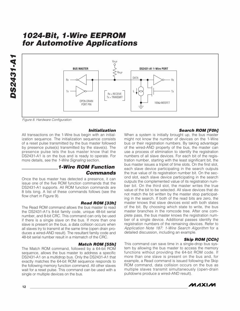
Hardware ConfigurationThe 1-Wire bus has only a single line by definition; it isimportant that each device on the bus be able to driveit at the appropriate time. To facilitate this, each deviceattached to the 1-Wire bus must have open-drain orthree-state outputs. The 1-Wire port of the DS2431-A1is open drain with an internal circuit equivalent to thatshown in Figure 8.
A multidrop bus consists of a 1-Wire bus with multipleslaves attached. The DS2431-A1 communicates at amaximum data rate of 15.4kbps. Note that legacy1-Wire products support a standard communicationspeed of 16.3kbps. The slightly reduced rates for theDS2431-A1 are a result of additional recovery times,which in turn were driven by a 1-Wire physical interfaceenhancement to improve noise immunity. The value ofthe pullup resistor primarily depends on the networksize and load conditions. The DS2431-A1 requires apullup resistor of 2.2kΩ (max).
The idle state for the 1-Wire bus is high. If for any rea-son a transaction needs to be suspended, the busMUST be left in the idle state if the transaction is toresume. If this does not occur and the bus is left low formore than 120µs, one or more devices on the busmight be reset.
Transaction SequenceThe protocol for accessing the DS2431-A1 through the 1-Wire port is as follows:
• Initialization
• ROM Function Command
• Memory Function Command
• Transaction/Data
DS
24
31
-A1
1024-Bit, 1-Wire EEPROMfor Automotive Applications
______________________________________________________________________________________ 11
DS
24
31
-A1
InitializationAll transactions on the 1-Wire bus begin with an initial-ization sequence. The initialization sequence consistsof a reset pulse transmitted by the bus master followedby presence pulse(s) transmitted by the slave(s). Thepresence pulse lets the bus master know that theDS2431-A1 is on the bus and is ready to operate. Formore details, see the 1-Wire Signaling section.
1-Wire ROM FunctionCommands
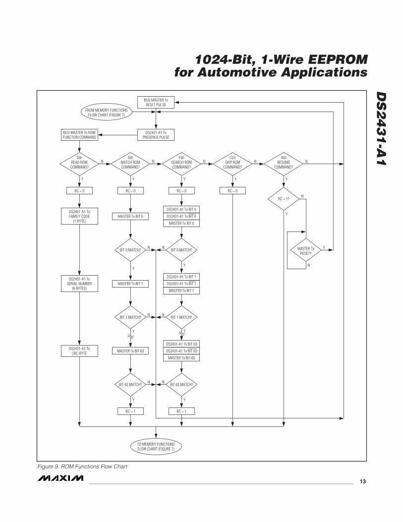
Once the bus master has detected a presence, it canissue one of the five ROM function commands that theDS2431-A1 supports. All ROM function commands are8 bits long. A list of these commands follows (see theflow chart in Figure 9).
Read ROM [33h]The Read ROM command allows the bus master to readthe DS2431-A1’s 8-bit family code, unique 48-bit serialnumber, and 8-bit CRC. This command can only be usedif there is a single slave on the bus. If more than oneslave is present on the bus, a data collision occurs whenall slaves try to transmit at the same time (open drain pro-duces a wired-AND result). The resultant family code and48-bit serial number result in a mismatch of the CRC.
Match ROM [55h]The Match ROM command, followed by a 64-bit ROMsequence, allows the bus master to address a specificDS2431-A1 on a multidrop bus. Only the DS2431-A1 thatexactly matches the 64-bit ROM sequence responds tothe following memory function command. All other slaveswait for a reset pulse. This command can be used with asingle or multiple devices on the bus.
Search ROM [F0h]When a system is initially brought up, the bus mastermight not know the number of devices on the 1-Wirebus or their registration numbers. By taking advantageof the wired-AND property of the bus, the master canuse a process of elimination to identify the registrationnumbers of all slave devices. For each bit of the regis-tration number, starting with the least significant bit, thebus master issues a triplet of time slots. On the first slot,each slave device participating in the search outputsthe true value of its registration number bit. On the sec-ond slot, each slave device participating in the searchoutputs the complemented value of its registration num-ber bit. On the third slot, the master writes the truevalue of the bit to be selected. All slave devices that donot match the bit written by the master stop participat-ing in the search. If both of the read bits are zero, themaster knows that slave devices exist with both statesof the bit. By choosing which state to write, the busmaster branches in the romcode tree. After one com-plete pass, the bus master knows the registration num-ber of a single device. Additional passes identify theregistration numbers of the remaining devices. Refer toApplication Note 187: 1-Wire Search Algorithm for adetailed discussion, including an example.
Skip ROM [CCh]This command can save time in a single-drop bus sys-tem by allowing the bus master to access the memoryfunctions without providing the 64-bit ROM code. Ifmore than one slave is present on the bus and, forexample, a Read command is issued following the SkipROM command, data collision occurs on the bus asmultiple slaves transmit simultaneously (open-drainpulldowns produce a wired-AND result).
1024-Bit, 1-Wire EEPROMfor Automotive Applications
12 ______________________________________________________________________________________
Rx
RPUP
IL
VPUP
BUS MASTER
OPEN-DRAINPORT PIN 100Ω MOSFET
Tx
Rx
Tx
DATA
DS2431-A1 1-Wire PORT
Rx = RECEIVETx = TRANSMIT
Figure 8. Hardware Configuration
DS
24
31
-A1
1024-Bit, 1-Wire EEPROMfor Automotive Applications
______________________________________________________________________________________ 13
DS2431-A1 TxPRESENCE PULSE
BUS MASTER TxRESET PULSE
BUS MASTER Tx ROMFUNCTION COMMAND
DS2431-A1 TxCRC BYTE
DS2431-A1 TxFAMILY CODE
(1 BYTE)
DS2431-A1 TxSERIAL NUMBER
(6 BYTES)
RC = 0
MASTER Tx BIT 0
RC = 0 RC = 0 RC = 0
YYY
Y
Y
Y
Y
33hREAD ROM
COMMAND?N
55hMATCH ROMCOMMAND?
BIT 0 MATCH? BIT 0 MATCH?
N
N N
N N
N N
F0hSEARCH ROMCOMMAND?
NCCh
SKIP ROMCOMMAND?
N
RC = 1
MASTER Tx BIT 1
MASTER Tx BIT 63
BIT 1 MATCH?
BIT 63 MATCH?
Y
Y
RC = 1
FROM MEMORY FUNCTIONSFLOW CHART (FIGURE 7)
TO MEMORY FUNCTIONSFLOW CHART (FIGURE 7)
DS2431-A1 Tx BIT 0
DS2431-A1 Tx BIT 0
MASTER Tx BIT 0
BIT 1 MATCH?
BIT 63 MATCH?
DS2431-A1 Tx BIT 1
DS2431-A1 Tx BIT 1
MASTER Tx BIT 1
DS2431-A1 Tx BIT 63
DS2431-A1 Tx BIT 63
MASTER Tx BIT 63
Y
RC = 1?
Y
A5hRESUME
COMMAND?N
N
Y
YMASTER TxRESET?
N
Figure 9. ROM Functions Flow Chart
Resume [A5h]To maximize the data throughput in a multidrop envi-ronment, the Resume function is available. This functionchecks the status of the RC bit and, if it is set, directlytransfers control to the Memory functions, similar to aSkip ROM command. The only way to set the RC bit isthrough successfully executing the Match ROM orSearch ROM command. Once the RC bit is set, thedevice can repeatedly be accessed through theResume command function. Accessing another deviceon the bus clears the RC bit, preventing two or moredevices from simultaneously responding to the Resumecommand function.
1-Wire SignalingThe DS2431-A1 requires strict protocols to ensure dataintegrity. The protocol consists of four types of signal-ing on one line: reset sequence with reset pulse andpresence pulse, write-zero, write-one, and read-data.Except for the presence pulse, the bus master initiatesall falling edges.
To get from idle to active, the voltage on the 1-Wire lineneeds to fall from VPUP below the threshold VTL. To getfrom active to idle, the voltage needs to rise from VILMAX past the threshold VTH. The time it takes for thevoltage to make this rise is seen in Figure 10 as ε, andits duration depends on the pullup resistor (RPUP) usedand the capacitance of the 1-Wire network attached.The voltage VILMAX is relevant for the DS2431-A1 whendetermining a logical level, not triggering any events.
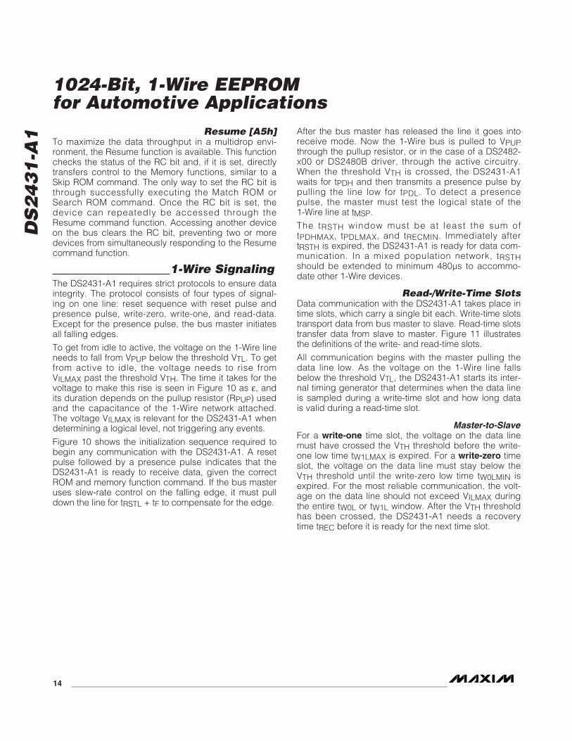
Figure 10 shows the initialization sequence required tobegin any communication with the DS2431-A1. A resetpulse followed by a presence pulse indicates that theDS2431-A1 is ready to receive data, given the correctROM and memory function command. If the bus masteruses slew-rate control on the falling edge, it must pulldown the line for tRSTL + tF to compensate for the edge.
After the bus master has released the line it goes intoreceive mode. Now the 1-Wire bus is pulled to VPUPthrough the pullup resistor, or in the case of a DS2482-x00 or DS2480B driver, through the active circuitry.When the threshold VTH is crossed, the DS2431-A1waits for tPDH and then transmits a presence pulse bypulling the line low for tPDL. To detect a presencepulse, the master must test the logical state of the1-Wire line at tMSP.
The tRSTH window must be at least the sum oftPDHMAX, tPDLMAX, and tRECMIN. Immediately aftertRSTH is expired, the DS2431-A1 is ready for data com-munication. In a mixed population network, tRSTHshould be extended to minimum 480µs to accommo-date other 1-Wire devices.
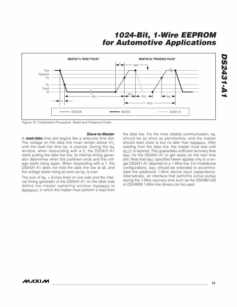
Read-/Write-Time SlotsData communication with the DS2431-A1 takes place intime slots, which carry a single bit each. Write-time slotstransport data from bus master to slave. Read-time slotstransfer data from slave to master. Figure 11 illustratesthe definitions of the write- and read-time slots.
All communication begins with the master pulling thedata line low. As the voltage on the 1-Wire line fallsbelow the threshold VTL, the DS2431-A1 starts its inter-nal timing generator that determines when the data lineis sampled during a write-time slot and how long datais valid during a read-time slot.
Master-to-SlaveFor a write-one time slot, the voltage on the data linemust have crossed the VTH threshold before the write-one low time tW1LMAX is expired. For a write-zero timeslot, the voltage on the data line must stay below theVTH threshold until the write-zero low time tW0LMIN isexpired. For the most reliable communication, the volt-age on the data line should not exceed VILMAX duringthe entire tW0L or tW1L window. After the VTH thresholdhas been crossed, the DS2431-A1 needs a recoverytime tREC before it is ready for the next time slot.
DS
24
31
-A1
1024-Bit, 1-Wire EEPROMfor Automotive Applications
14 ______________________________________________________________________________________
DS
24
31
-A1
1024-Bit, 1-Wire EEPROMfor Automotive Applications
______________________________________________________________________________________ 15
Slave-to-MasterA read-data time slot begins like a write-one time slot.The voltage on the data line must remain below VTLuntil the read low time tRL is expired. During the tRLwindow, when responding with a 0, the DS2431-A1starts pulling the data line low; its internal timing gener-ator determines when this pulldown ends and the volt-age starts rising again. When responding with a 1, theDS2431-A1 does not hold the data line low at all, andthe voltage starts rising as soon as tRL is over.
The sum of tRL + δ (rise time) on one side and the inter-nal timing generator of the DS2431-A1 on the other sidedefine the master sampling window (tMSRMIN totMSRMAX), in which the master must perform a read from
the data line. For the most reliable communication, tRLshould be as short as permissible, and the mastershould read close to but no later than tMSRMAX. Afterreading from the data line, the master must wait untiltSLOT is expired. This guarantees sufficient recovery timetREC for the DS2431-A1 to get ready for the next timeslot. Note that tREC specified herein applies only to a sin-gle DS2431-A1 attached to a 1-Wire line. For multideviceconfigurations, tREC should be extended to accommo-date the additional 1-Wire device input capacitance.Alternatively, an interface that performs active pullupduring the 1-Wire recovery time such as the DS2482-x00or DS2480B 1-Wire line drivers can be used.
RESISTOR MASTER DS2431-A1
tRSTL tPDL
tRSTH
tPDH
MASTER Tx "RESET PULSE" MASTER Rx "PRESENCE PULSE"
VPUPVIHMASTER
VTH
VTLVILMAX
0V
ε
tF
tREC
tMSP
Figure 10. Initialization Procedure: Reset and Presence Pulse
RESISTOR MASTER
RESISTOR MASTER
RESISTOR MASTER DS2431-A1
ε
ε
δ
VPUPVIHMASTER
VTH
VTLVILMAX
0VtF
VPUPVIHMASTER
VTH
VTLVILMAX
0V
tF
VPUPVIHMASTER
VTH
VTLVILMAX
0VtF
tSLOT
tW1L
tRECtSLOT
tSLOT
tW0L
tREC
MASTERSAMPLINGWINDOW
tRL
tMSR
WRITE-ONE TIME SLOT
WRITE-ZERO TIME SLOT
READ-DATA TIME SLOT
Figure 11. Read/Write Timing Diagrams
DS
24
31
-A1
1024-Bit, 1-Wire EEPROMfor Automotive Applications
16 ______________________________________________________________________________________
DS
24
31
-A1
1024-Bit, 1-Wire EEPROMfor Automotive Applications
______________________________________________________________________________________ 17
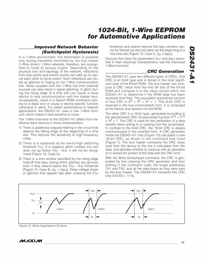
Improved Network Behavior(Switchpoint Hysteresis)
In a 1-Wire environment, line termination is possibleonly during transients controlled by the bus master (1-Wire driver). 1-Wire networks, therefore, are suscep-tible to noise of various origins. Depending on thephysical size and topology of the network, reflectionsfrom end points and branch points can add up or can-cel each other to some extent. Such reflections are visi-ble as glitches or ringing on the 1-Wire communicationline. Noise coupled onto the 1-Wire line from externalsources can also result in signal glitching. A glitch dur-ing the rising edge of a time slot can cause a slavedevice to lose synchronization with the master and,consequently, result in a Search ROM command com-ing to a dead end or cause a device-specific functioncommand to abort. For better performance in networkapplications, the DS2431-A1 uses a new 1-Wire front-end, which makes it less sensitive to noise.
The 1-Wire front-end of the DS2431-A1 differs from tra-ditional slave devices in three characteristics.
1) There is additional lowpass filtering in the circuit thatdetects the falling edge at the beginning of a timeslot. This reduces the sensitivity to high-frequencynoise.
2) There is a hysteresis at the low-to-high switchingthreshold VTH. If a negative glitch crosses VTH butdoes not go below VTH - VHY, it will not be recog-nized (Figure 12, Case A).
3) There is a time window specified by the rising edgehold-off time tREH during which glitches are ignored,even if they extend below the VTH - VHY threshold(Figure 12, Case B, tGL < tREH). Deep voltage dropsor glitches that appear late after crossing the VTH
threshold and extend beyond the tREH window can-not be filtered out and are taken as the beginning of anew time slot (Figure 12, Case C, tGL ≥ tREH).
Devices that have the parameters VHY and tREH speci-fied in their electrical characteristics use the improved1-Wire front-end.
CRC GenerationThe DS2431-A1 uses two different types of CRCs. OneCRC is an 8-bit type and is stored in the most signifi-cant byte of the 64-bit ROM. The bus master can com-pute a CRC value from the first 56 bits of the 64-bitROM and compare it to the value stored within theDS2431-A1 to determine if the ROM data has beenreceived error-free. The equivalent polynomial functionof this CRC is X8 + X5 + X4 + 1. This 8-bit CRC isreceived in the true (noninverted) form. It is computedat the factory and lasered into the ROM.
The other CRC is a 16-bit type, generated according tothe standardized CRC-16 polynomial function X16 + X15
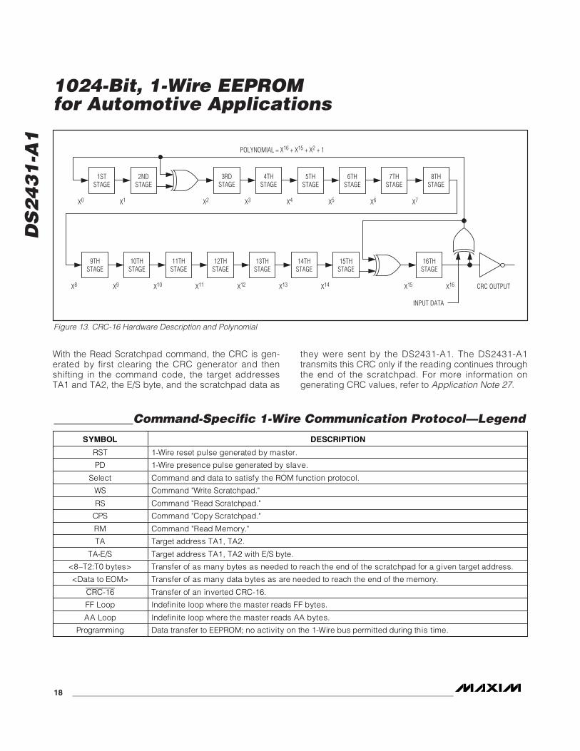
+ X2 + 1. This CRC is used for fast verification of a datatransfer when writing to or reading from the scratchpad.In contrast to the 8-bit CRC, the 16-bit CRC is alwayscommunicated in the inverted form. A CRC generatorinside the DS2431-A1 chip (Figure 13) calculates a new16-bit CRC, as shown in the command flow chart(Figure 7). The bus master compares the CRC valueread from the device to the one it calculates from thedata, and decides whether to continue with an operationor to reread the portion of the data with the CRC error.
With the Write Scratchpad command, the CRC is gen-erated by first clearing the CRC generator and thenshifting in the command code, the target addressesTA1 and TA2, and all the data bytes as they were sentby the bus master. The DS2431-A1 transmits this CRConly if E2:E0 = 111b.
VPUP
VTHVHY
0V
tREH
tGL
tREH
tGL
CASE A CASE CCASE B
Figure 12. Noise Suppression Scheme
With the Read Scratchpad command, the CRC is gen-erated by first clearing the CRC generator and thenshifting in the command code, the target addressesTA1 and TA2, the E/S byte, and the scratchpad data as
they were sent by the DS2431-A1. The DS2431-A1transmits this CRC only if the reading continues throughthe end of the scratchpad. For more information ongenerating CRC values, refer to Application Note 27.
1STSTAGE
2NDSTAGE
3RDSTAGE
4THSTAGE
7THSTAGE
8THSTAGE
6THSTAGE
5THSTAGE
X0 X1 X2 X3 X4
POLYNOMIAL = X16 + X15 + X2 + 1
INPUT DATA
CRC OUTPUT
X5 X6
11THSTAGE
12THSTAGE
15THSTAGE
14THSTAGE
13THSTAGE
X11 X12
9THSTAGE
10THSTAGE
X9 X10 X13 X14
X7
16THSTAGE
X16X15X8
Figure 13. CRC-16 Hardware Description and Polynomial
Command-Specific 1-Wire Communication Protocol—Legend
SYMBOL DESCRIPTION
RST 1-Wire reset pulse generated by master.
PD 1-Wire presence pulse generated by slave.
Select Command and data to satisfy the ROM function protocol.
WS Command "Write Scratchpad."
RS Command "Read Scratchpad."
CPS Command "Copy Scratchpad."
RM Command "Read Memory."
TA Target address TA1, TA2.
TA-E/S Target address TA1, TA2 with E/S byte.
<8–T2:T0 bytes> Transfer of as many bytes as needed to reach the end of the scratchpad for a given target address.
<Data to EOM> Transfer of as many data bytes as are needed to reach the end of the memory.
CRC-16 Transfer of an inverted CRC-16.
FF Loop Indefinite loop where the master reads FF bytes.
AA Loop Indefinite loop where the master reads AA bytes.
Programming Data transfer to EEPROM; no activity on the 1-Wire bus permitted during this time.
DS
24
31
-A1
1024-Bit, 1-Wire EEPROMfor Automotive Applications
18 ______________________________________________________________________________________
DS
24
31
-A1
1024-Bit, 1-Wire EEPROMfor Automotive Applications
______________________________________________________________________________________ 19
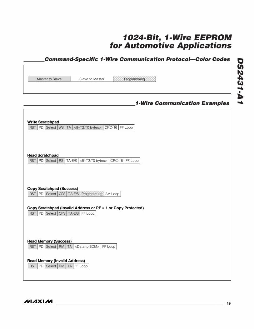
Command-Specific 1-Wire Communication Protocol—Color Codes
1-Wire Communication Examples
Master to Slave Slave to Master Programming
Write Scratchpad RST PD Select WS TA <8–T2:T0 bytes> CRC-16 FF Loop
Read Scratchpad RST PD Select RS TA-E/S <8–T2:T0 bytes> CRC-16 FF Loop
Copy Scratchpad (Success) RST PD Select CPS TA-E/S Programming AA Loop
Copy Scratchpad (Invalid Address or PF = 1 or Copy Protected) RST PD Select CPS TA-E/S FF Loop
Read Memory (Success) RST PD Select RM TA <Data to EOM> FF Loop
Read Memory (Invalid Address) RST PD Select RM TA FF Loop
DS
24
31
-A1
1024-Bit, 1-Wire EEPROMfor Automotive Applications
20 ______________________________________________________________________________________
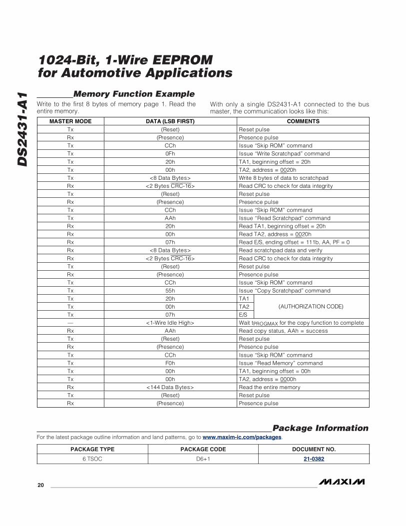
Memory Function ExampleWrite to the first 8 bytes of memory page 1. Read theentire memory.
With only a single DS2431-A1 connected to the busmaster, the communication looks like this:
MASTER MODE DATA (LSB FIRST) COMMENTS Tx (Reset) Reset pulse Rx (Presence) Presence pulse Tx CCh Issue “Skip ROM” command Tx 0Fh Issue “Write Scratchpad” command Tx 20h TA1, beginning offset = 20h Tx 00h TA2, address = 0020h Tx <8 Data Bytes> Write 8 bytes of data to scratchpad Rx <2 Bytes CRC-16> Read CRC to check for data integrity Tx (Reset) Reset pulse Rx (Presence) Presence pulse Tx CCh Issue “Skip ROM” command Tx AAh Issue “Read Scratchpad” command Rx 20h Read TA1, beginning offset = 20h Rx 00h Read TA2, address = 0020h Rx 07h Read E/S, ending offset = 111b, AA, PF = 0 Rx <8 Data Bytes> Read scratchpad data and verify Rx <2 Bytes CRC-16> Read CRC to check for data integrity Tx (Reset) Reset pulse Rx (Presence) Presence pulse Tx CCh Issue “Skip ROM” command Tx 55h Issue “Copy Scratchpad” command Tx 20h TA1 Tx 00h TA2 Tx 07h E/S
(AUTHORIZATION CODE)
— <1-Wire Idle High> Wait tPROGMAX for the copy function to complete Rx AAh Read copy status, AAh = success Tx (Reset) Reset pulse Rx (Presence) Presence pulse Tx CCh Issue “Skip ROM” command Tx F0h Issue “Read Memory” command Tx 00h TA1, beginning offset = 00h Tx 00h TA2, address = 0000h Rx <144 Data Bytes> Read the entire memory Tx (Reset) Reset pulse Rx (Presence) Presence pulse
PACKAGE TYPE PACKAGE CODE DOCUMENT NO.
6 TSOC D6+1 21-0382
Package InformationFor the latest package outline information and land patterns, go to www.maxim-ic.com/packages.
DS
24
31
-A1
1024-Bit, 1-Wire EEPROMfor Automotive Applications
Maxim cannot assume responsibility for use of any circuitry other than circuitry entirely embodied in a Maxim product. No circuit patent licenses areimplied. Maxim reserves the right to change the circuitry and specifications without notice at any time.
Maxim Integrated Products, 120 San Gabriel Drive, Sunnyvale, CA 94086 408-737-7600 ____________________ 21
© 2008 Maxim Integrated Products Maxim is a registered trademark of Maxim Integrated Products, Inc.
Revision HistoryREVISION NUMBER
REVISION DATE
DESCRIPTIONPAGES
CHANGED
0 11/07 Initial release. —
1 3/08 Removed all references to overdrive speed. 1–5, 8, 11, 13, 14, 15, 18