Embed Size (px)
Citation preview

1
Understanding Current Sensing Applications & How to Choose the Right DevicePete Semig
Applications Engineer-Precision Linear

2
Outline & Presentation Goals
• Outline– Fundamentals
– Devices
– Accuracy
– PCB Layout & Troubleshooting
• Goals of this presentation– Select a current sensing topology (direct vs. indirect, high vs. low-side, etc.)
– Select the appropriate device (op amp, difference amp, inst. amp, or CSM?)
– Calculate the accuracy of their solution
– Troubleshoot a design (is the device out of specification?)

Fundamentals
3

4
Indirect Sensing
• Based on Ampere’s and Faraday’s Laws
• Noninvasive
• Inherently isolated
• No power lost by the system
• Recommend– Very high currents (e.g. >100A)– Very high voltage– Very dynamic load currents– Isolation required
loadIr2
IB loado
5
Indirect Sensing-Solutions
• Hall Effect Sensor– ADS1208, ADS1205, ADS7861, ADS8361, ADS8365
– Application note SLAA286

6
Indirect Sensing-Solutions
• VAC Sensor– DRV401 is a custom solution for VAC Sensors
– Combine with SAR ADC (e.g. ADS8509)
– Less sensitive to temperature drift and initial offset than Hall sensor solutions

7
Direct Sensing
shuntR+
-
loadI
shuntV+
GND
+
-
oV
• Based on Ohm’s Law
• Shunt resistor in series with load
• Invasive
• Power dissipated by Rshunt
• Sensing circuit not isolated from system load
• Recommend– Smaller currents (<100A)– System can tolerate power loss– Low voltage– Load current not very dynamic– Isolation not required (though it can
be accomplished)
Differential Amplifier
8
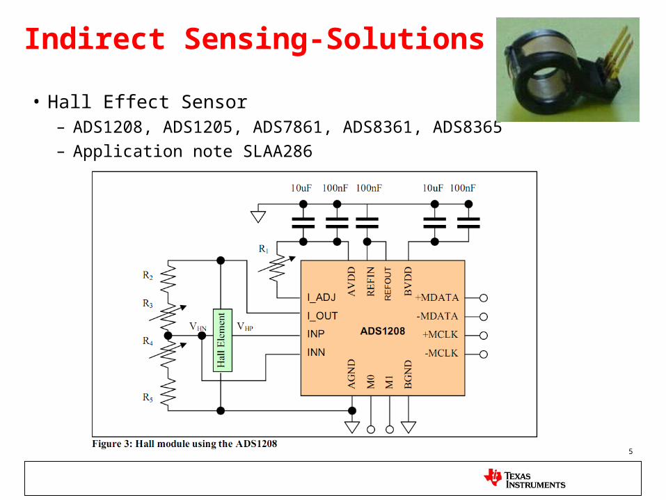
Differential Input Amplifier
• Differential input amplifiers are devices/circuits that can input and amplify differential signals while suppressing common-mode signals– This includes operational amplifiers, instrumentation amplifiers, difference
amplifiers, and current-shunt monitors
Difference
Amplifier
Instrumentation AmplifiersOperational
Amplifier
CSM

9
Common-Mode Voltage
+
+
–
+
–
GNDGND
pV nV
GND
+
-
oV
2
VVV
npcm
+
+
– 2
VidGND
+
-dmido AVV
+
–
GND
+
–
2
Vid
cmV
+
-idV
DifferentialAmplifier
dmAGain alDifferenti
10
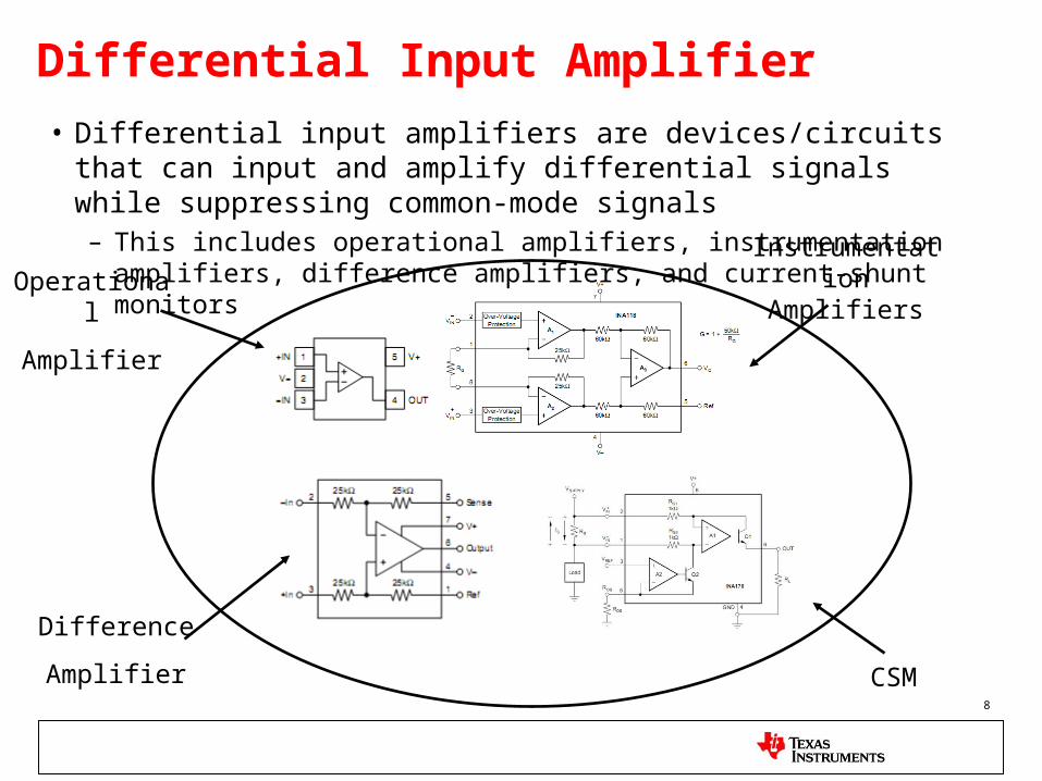
Low-Side Sensing
• Shunt resistor placed between the system load and ground
• Pros– Vcm≈0V– Straightforward– Inexpensive (may use an op amp)
• Cons– Can’t detect load shorts to ground– Single-ended measurement (stay
tuned)– System GND is now Iload*Rshunt
SystemLoad
+
–busV
shuntR+
-
loadI
shuntV
GND
+
GND
+
-
oV
DifferentialAmplifier
GNDVcm
11
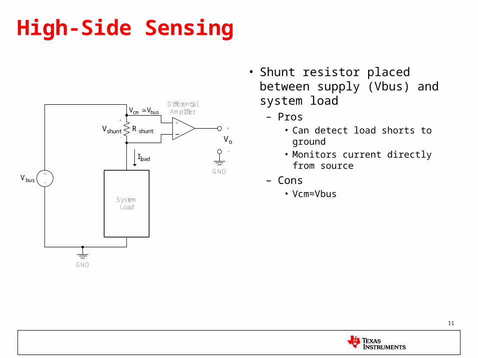
High-Side Sensing
busV
SystemLoad
+
–
shuntR+
-
loadI
shuntV+
GND
+
-
oV
GND
DifferentialAmplifierbuscm VV
• Shunt resistor placed between supply (Vbus) and system load
– Pros• Can detect load shorts to ground• Monitors current directly from source
– Cons• Vcm≈Vbus

12
Directionality
• Application may require sensing current in both directions
busV
SystemLoad
+
–
shuntR+
-
loadI
shuntV+
GND
+
-
oV
GND
DifferentialAmplifier
refV
oV
refV
System Sinking
System Sourcing

13
Output
• Op amps, difference amplifiers, and instrumentation amplifiers have voltage outputs
• Current shunt monitors can also have current-output and digital-output
INA138/168

Devices
14
15
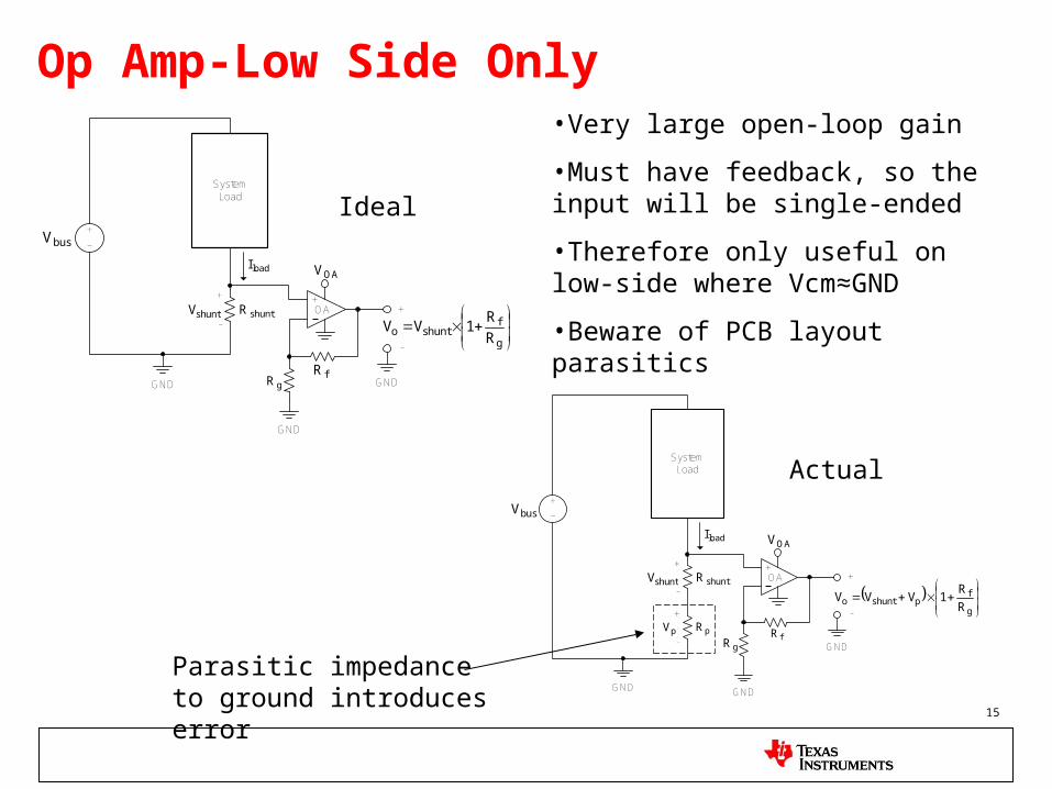
Op Amp-Low Side Only
SystemLoad
+
–busV
shuntR+
-
loadI
shuntV+
GND
+
-
g
fshunto R
R1VV
OA
GND
GND
fRgR
OAV
SystemLoad
+
–busV
shuntR+
-
loadI
shuntV+
GND
+
-
g
fpshunto R
R1VVV
OA
GND GND
fRgR
OAV
pR+
-pV
Ideal
Actual
Parasitic impedance to ground introduces error
•Very large open-loop gain
•Must have feedback, so the input will be single-ended
•Therefore only useful on low-side where Vcm≈GND
•Beware of PCB layout parasitics
16
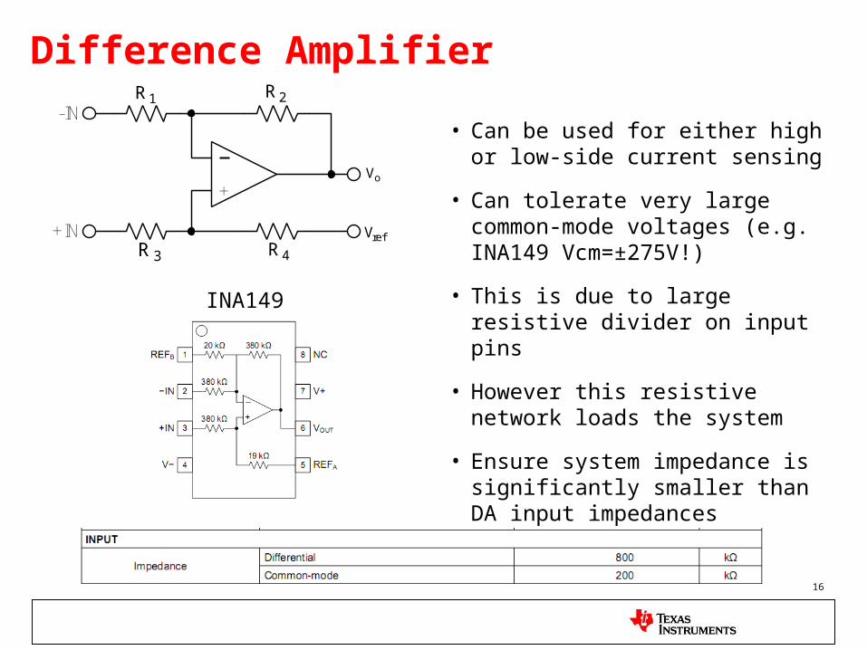
Difference Amplifier
+
+IN
-IN1R 2R
3R 4R
oV
refV
• Can be used for either high or low-side current sensing
• Can tolerate very large common-mode voltages (e.g. INA149 Vcm=±275V!)
• This is due to large resistive divider on input pins
• However this resistive network loads the system
• Ensure system impedance is significantly smaller than DA input impedances
INA149
17
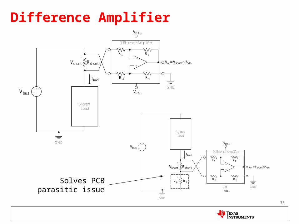
Difference Amplifier
busV
SystemLoad
+
–
shuntR+
-
loadI
shuntV
GND
dmshunto AVV +
1R 2R
3R 4R
GND
Difference Amplifier
DAV
DAV
SystemLoad
+
–busV
shuntR+
-
loadI
shuntV dmshunto AVV
GND
pR+
-pV
+
1R 2R
3R 4R
GND
Difference Amplifier
DAV
DAV
Solves PCB parasitic issue

18
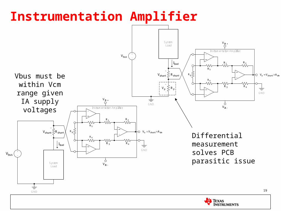
Instrumentation Amplifier
• A three op amp IA is made of a DA with buffered inputs
• Pros– Large input impedance– Change gain with external resistor
• Cons– Common-mode voltage must remain
within supply voltage
• Usually used for low-side sensing, but can be used for high-side depending on common-mode voltage
+
1R 2R
3R 4R
oV
refV
+
gR
+
+IN
-IN
5R
6R
19
Instrumentation Amplifier
SystemLoad
+
–busV
shuntR+
-
loadI
shuntV dmshunto AVV
GND
pR+
-pV
+
1R 2R
3R 4R
+
gR
+
5R
6R
Instrumentation Amplifier
GND
IAV
IAV
busV
SystemLoad
+
–
shuntR+
-
loadI
shuntV
GND
dmshunto AVV +
1R 2R
3R 4R
+
gR
+
5R
6R
Instrumentation Amplifier
GND
IAV
IAV
Vbus must be within Vcm range given IA supply
voltages
Differential measurement solves PCB parasitic issue
20
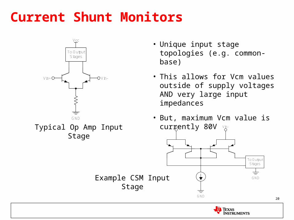
Current Shunt Monitors
• Unique input stage topologies (e.g. common-base)
• This allows for Vcm values outside of supply voltages AND very large input impedances
• But, maximum Vcm value is currently 80V
To Output Stages
GND
Vin+ Vin-
Vcc
GND
Vin+ Vin-
To Output Stages
GND
Typical Op Amp Input Stage
Example CSM Input Stage

21
Input and Output Voltage Range
• Always ensure that desired input and output voltage ranges are within datasheet specifications
• Instrumentation amplifiers can be tricky
• For example, can we effectively use the INA826 for a low-side current measurement (Vcm≈0V)?
22
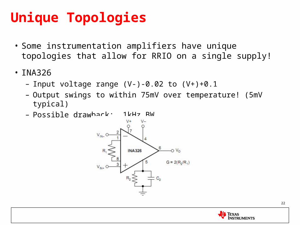
Unique Topologies
• Some instrumentation amplifiers have unique topologies that allow for RRIO on a single supply!
• INA326– Input voltage range (V-)-0.02 to (V+)+0.1
– Output swings to within 75mV over temperature! (5mV typical)
– Possible drawback: 1kHz BW
23
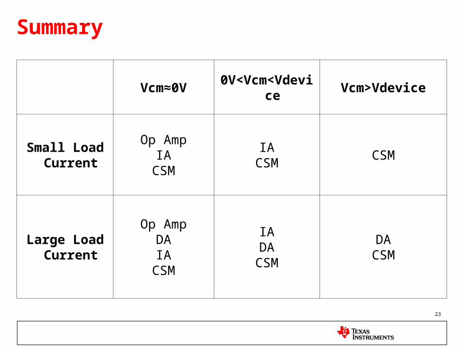
Summary
Vcm≈0V 0V<Vcm<Vdevice Vcm>Vdevice
Small Load Current
Op AmpIA
CSM
IACSM CSM
Large Load Current
Op AmpDAIA
CSM
IADA
CSM
DACSM

Accuracy
24

25
Accuracy
• Definition– Worst case
– Probable (Root-sum-square)
n
1
ncaseworst e100%
n
1
2nRSS e100%
Error Sources
26
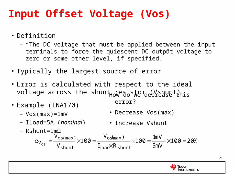
Input Offset Voltage (Vos)
• Definition– “The DC voltage that must be applied between the input terminals to force
the quiescent DC output voltage to zero or some other level, if specified.”
• Typically the largest source of error
• Error is calculated with respect to the ideal voltage across the shunt resistor (Vshunt)
• Example (INA170)– Vos(max)=1mV
– Iload=5A (nominal)
– Rshunt=1mΩ
%20100
mV5
mV1100
RI
V100
V
Ve
shuntload
maxos
shunt
(max)osVos
How do we decrease this error?
• Decrease Vos(max)
• Increase Vshunt

27
Common-mode Rejection Ratio (CMRR)
• Measure of a device’s ability to reject common-mode signals
• Otherwise the common-mode signals can manifest themselves into differential signals which add to the error
• Specified one of two ways– Linear: μV/V
• Worst case is the maximum value
– Logarithmic: dB• Worst case is the minimum value
• Need the following to calculate error– Worst case specification
– Common-mode test condition from datasheet (Vcm-pds)
– System common-mode voltage (Vcm-sys)
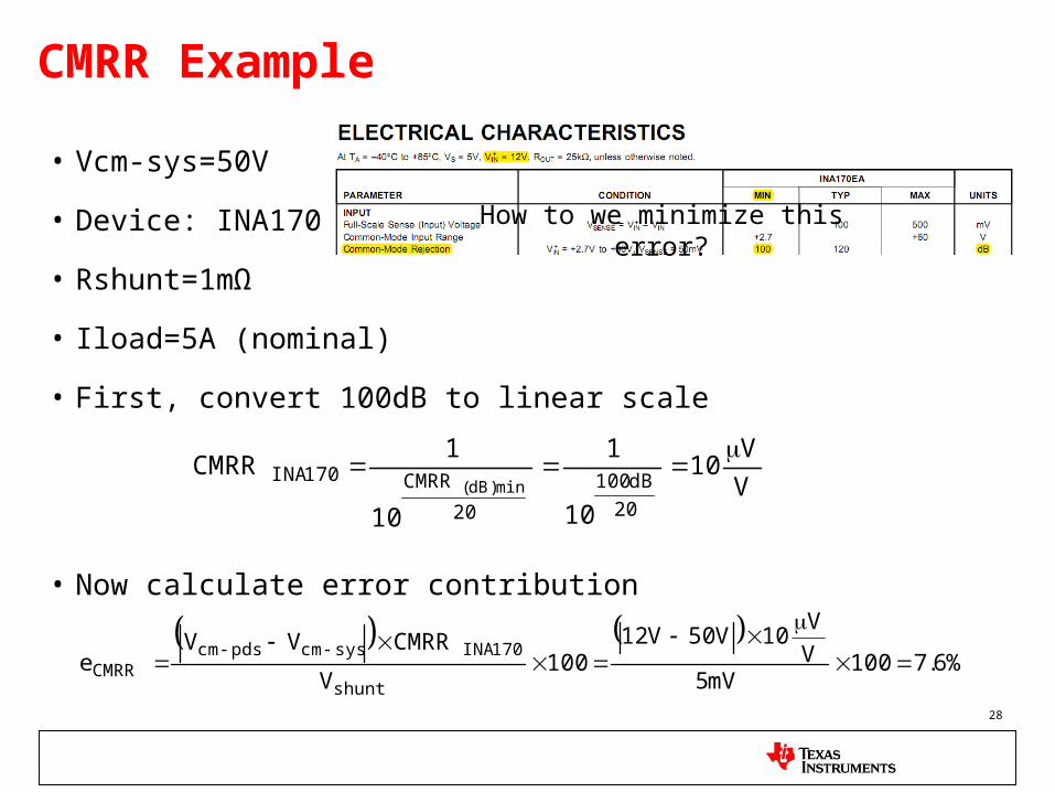
28
CMRR Example
• Vcm-sys=50V
• Device: INA170
• Rshunt=1mΩ
• Iload=5A (nominal)
• First, convert 100dB to linear scale
• Now calculate error contribution
V
V10
10
1
10
1CMRR
20
dB100
20
CMRR170INAmin)dB(
%6.7100
mV5V
V10V50V12
100V
CMRRVVe
shunt
170INAsyscmpdscmCMRR
How to we minimize this error?
29
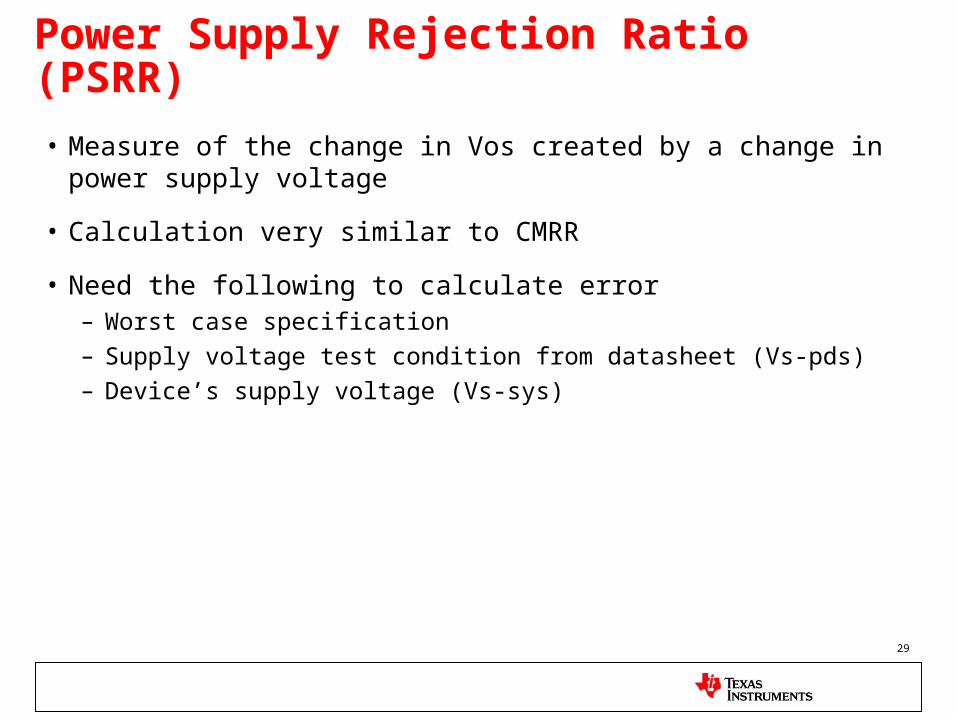
Power Supply Rejection Ratio (PSRR)
• Measure of the change in Vos created by a change in power supply voltage
• Calculation very similar to CMRR
• Need the following to calculate error– Worst case specification
– Supply voltage test condition from datasheet (Vs-pds)
– Device’s supply voltage (Vs-sys)
30
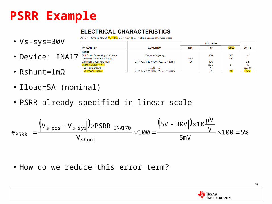
PSRR Example
• Vs-sys=30V
• Device: INA170
• Rshunt=1mΩ
• Iload=5A (nominal)
• PSRR already specified in linear scale
• How do we reduce this error term?
%5100
mV5V
V10V30V5
100V
PSRRVVe
shunt
170INAsysspdssPSRR

31
Other Errors
• Gain error– Usually listed in datasheet as a percentage
• Shunt resistor tolerance– Usually given as a percentage. Beware of temperature drift, though.
• Vos drift– Usually listed in datasheet as μV/˚C– Multiply specification by maximum deviation from 25C
• Vos shift– Change in Vos due to time– Usually not specified. Most likely never guaranteed.– Rule of thumb: In 10 years, Vos may shift no more than the Vos(max)
specification.– This is in addition to the device’s initial Vos specification.
32
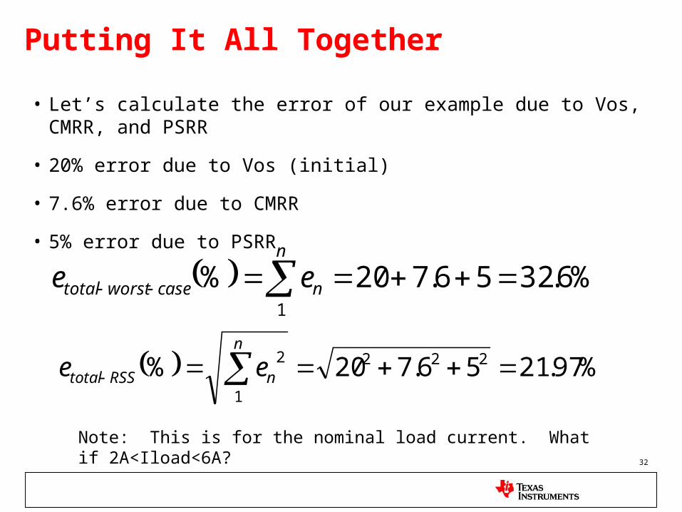
Putting It All Together
• Let’s calculate the error of our example due to Vos, CMRR, and PSRR
• 20% error due to Vos (initial)
• 7.6% error due to CMRR
• 5% error due to PSRR
%6.3256.720%1
n
ncaseworsttotal ee
%97.2156.720% 222
1
2
n
nRSStotal ee
Note: This is for the nominal load current. What if 2A<Iload<6A?

PCB Layout and Troubleshooting
33
34
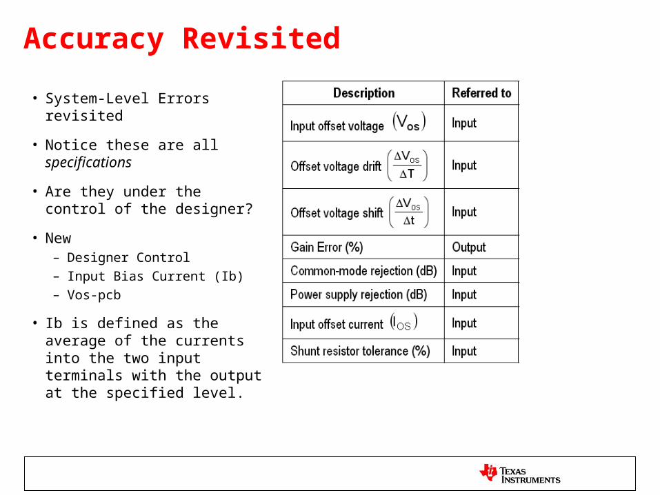
Accuracy Revisited
• System-Level Errors revisited
• Notice these are all specifications
• Are they under the control of the designer?
• New– Designer Control– Input Bias Current (Ib)– Vos-pcb
• Ib is defined as the average of the currents into the two input terminals with the output at the specified level.
35
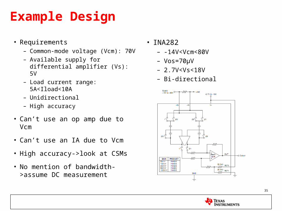
Example Design
• Requirements– Common-mode voltage (Vcm): 70V– Available supply for differential
amplifier (Vs): 5V– Load current range: 5A<Iload<10A– Unidirectional– High accuracy
• Can’t use an op amp due to Vcm
• Can’t use an IA due to Vcm
• High accuracy->look at CSMs
• No mention of bandwidth->assume DC measurement
• INA282– -14V<Vcm<80V– Vos=70μV– 2.7V<Vs<18V– Bi-directional
36
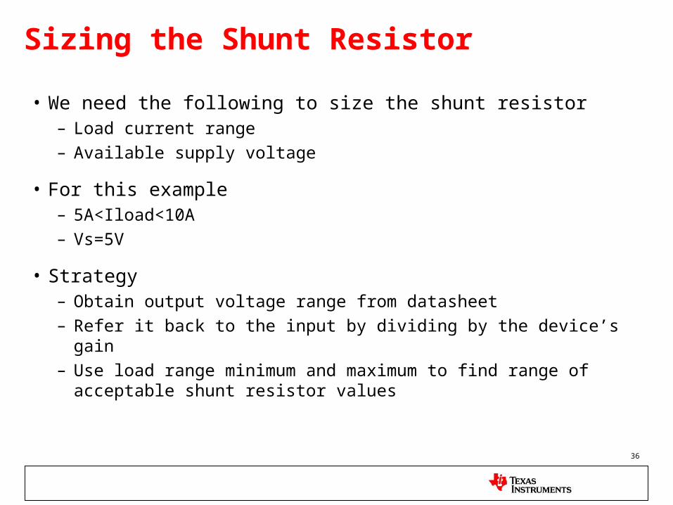
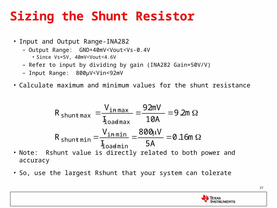
Sizing the Shunt Resistor
• We need the following to size the shunt resistor– Load current range
– Available supply voltage
• For this example – 5A<Iload<10A
– Vs=5V
• Strategy– Obtain output voltage range from datasheet
– Refer it back to the input by dividing by the device’s gain
– Use load range minimum and maximum to find range of acceptable shunt resistor values
37
Sizing the Shunt Resistor
• Input and Output Range-INA282– Output Range: GND+40mV<Vout<Vs-0.4V
• Since Vs=5V, 40mV<Vout<4.6V
– Refer to input by dividing by gain (INA282 Gain=50V/V)– Input Range: 800μV<Vin<92mV
• Calculate maximum and minimum values for the shunt resistance
• Note: Rshunt value is directly related to both power and accuracy
• So, use the largest Rshunt that your system can tolerate
m16.0A5
V800
I
VR
m2.9A10
mV92
I
VR
minload
mininminshunt
maxload
maxinmaxshunt
38
Example Simulation
Vs 5R1 10k
-
+Vout
Rshunt 8m
V+
In+ In-
Out
Ref1Ref2Gnd
U1 INA282
Iload
Vcm 70 5A<Iload<10A
T
Load current (A)
5.0 6.0 7.0 8.0 9.0 10.0
Out
put
Vol
tage
(V
)
2.0
2.5
3.0
3.5
4.0

39
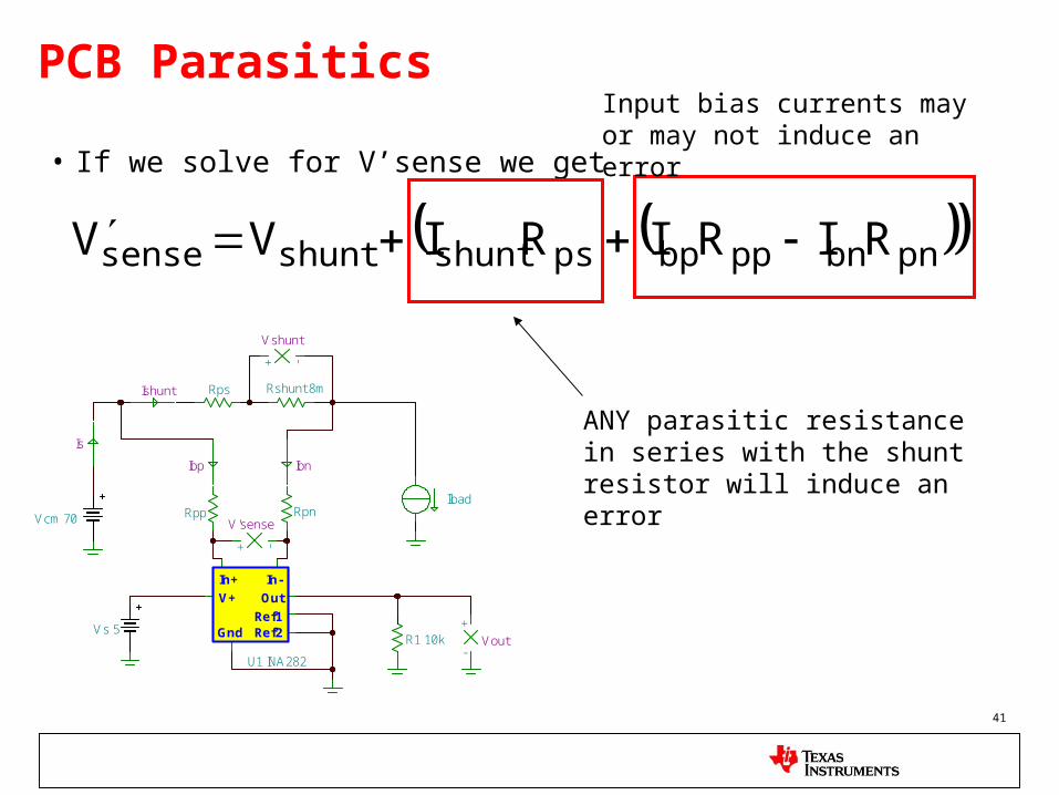
PCB Parasitics
• There are 3 parasitic resistances that can affect the accuracy
Vs 5R1 10k
-
+Vout
Rshunt 8m
V+
In+ In-
Out
Ref1Ref2Gnd
U1 INA282
Iload
Vcm 70
Rps
Rpp Rpn
-+
Vshunt
-+V'sense
Ibp Ibn
Is
Ishunt
In series with the shunt (load current) In series with the
device inputs (input bias current)

40
PCB Parasitics
• Ideally Vshunt=Vsense
• Vsense is the voltage at the pins of the device
• However, the parasitics cause Vshunt≠Vsense, so we will rename the voltage at the pins to V’sense
Vs 5R1 10k
-
+Vout
Rshunt 8m
V+
In+ In-
Out
Ref1Ref2Gnd
U1 INA282
Iload
Vcm 70
Rps
Rpp Rpn
-+
Vshunt
-+
V'sense
Ibp Ibn
Is
Ishunt
shunt
PCBOSPCB V
V100%e
senseshuntPCBOS VVV
Ideal Shunt Voltage
41
PCB Parasitics
• If we solve for V’sense we get
Vs 5R1 10k
-
+Vout
Rshunt 8m
V+
In+ In-
Out
Ref1Ref2Gnd
U1 INA282
Iload
Vcm 70
Rps
Rpp Rpn
-+
Vshunt
-+
V'sense
Ibp Ibn
Is
Ishunt
pnbnppbppsshuntshuntsense RIRIRIVV
ANY parasitic resistance in series with the shunt resistor will induce an error
Input bias currents may or may not induce an error
42
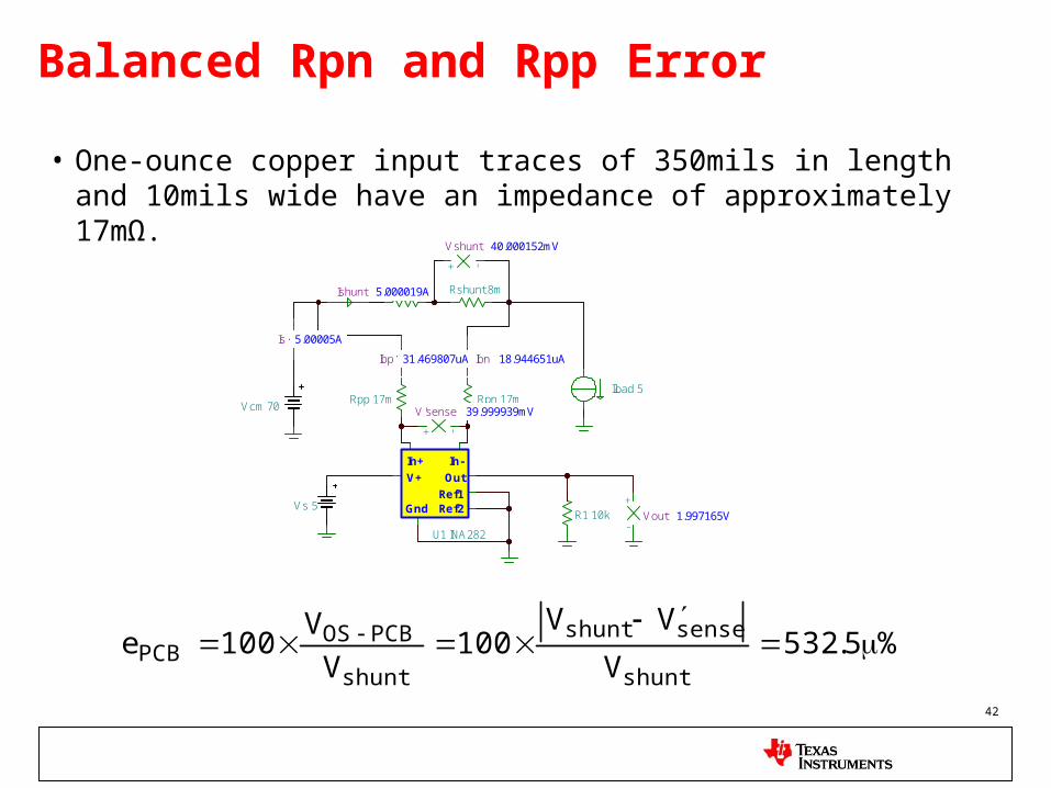
Balanced Rpn and Rpp Error
• One-ounce copper input traces of 350mils in length and 10mils wide have an impedance of approximately 17mΩ.
Vs 5R1 10k
-
+Vout
Rshunt 8m
V+
In+ In-
Out
Ref1Ref2Gnd
U1 INA282
Iload 5
Vcm 70
Rps 0
Rpp 17m Rpn 17m
-+
Vshunt
-+V'sense
Ibp Ibn
Is
Ishunt 5.000019A
5.00005A
18.944651uA31.469807uA
39.999939mV
40.000152mV
1.997165V
%5.532V
VV100
V
V100e
shunt
senseshunt
shunt
PCBOSPCB
43
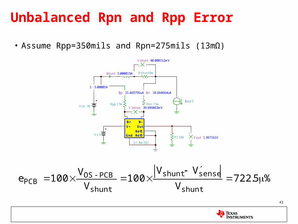
Unbalanced Rpn and Rpp Error
• Assume Rpp=350mils and Rpn=275mils (13mΩ)
%5.722V
VV100
V
V100e
shunt
senseshunt
shunt
PCBOSPCB
Vs 5R1 10k
-
+Vout
Rshunt 8m
V+
In+ In-
Out
Ref1Ref2Gnd
U1 INA282
Iload 5
Vcm 70
Rps 0
Rpp 17m Rpn 13m
-+
Vshunt
-+
V'sense
Ibp Ibn
Is
Ishunt 5.000019A
5.00005A
18.944664uA31.469795uA
39.999863mV
40.000152mV
1.997161V
44
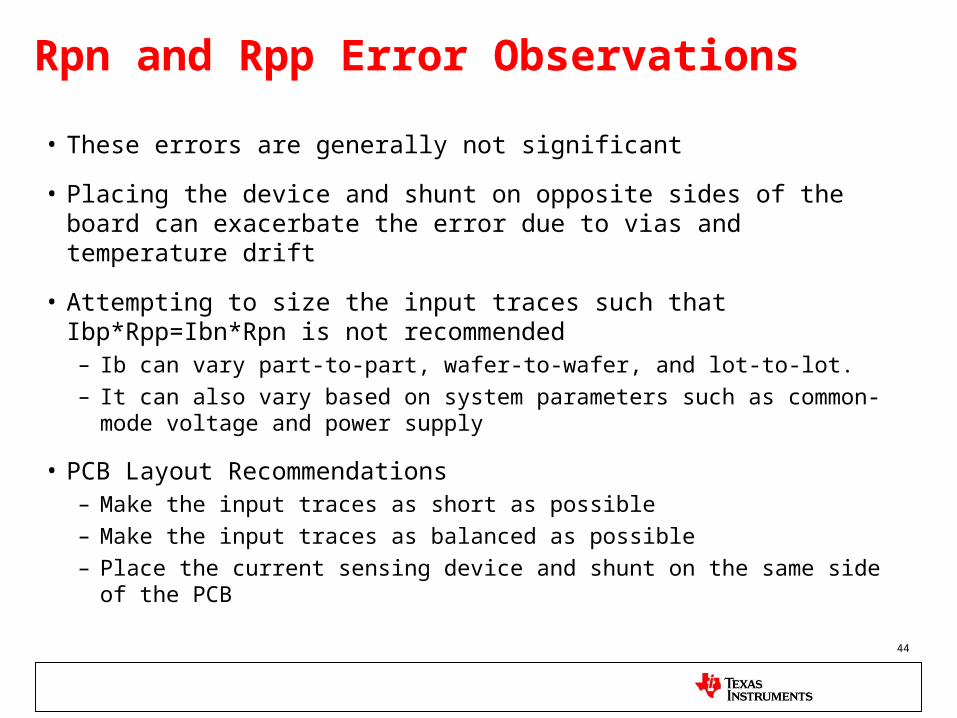
Rpn and Rpp Error Observations
• These errors are generally not significant
• Placing the device and shunt on opposite sides of the board can exacerbate the error due to vias and temperature drift
• Attempting to size the input traces such that Ibp*Rpp=Ibn*Rpn is not recommended– Ib can vary part-to-part, wafer-to-wafer, and lot-to-lot.
– It can also vary based on system parameters such as common-mode voltage and power supply
• PCB Layout Recommendations– Make the input traces as short as possible
– Make the input traces as balanced as possible
– Place the current sensing device and shunt on the same side of the PCB

45
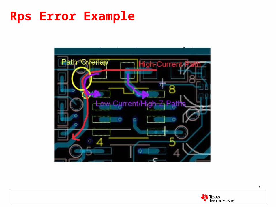
Rps Error
• ANY resistance in series with the shunt will induce an error
• One-ounce copper trace of 10mils in length and 25mils wide has an impedance of approximately 193μΩ. – Recall that Rps is in the high-current path
%41.2V
VV100
V
V100e
shunt
senseshunt
shunt
PCBOSPCB
2.41% error due to 193μΩ!
Vs 5R1 10k
-
+Vout
Rshunt 8m
V+
In+ In-
Out
Ref1Ref2Gnd
U1 INA282
Iload 10
Vcm 70
Rps 193u
Rpp 0 Rpn 0
-+
Vshunt
-+
V'sense
Ibp Ibn
Is
Ishunt 10.000012A
10.00005A
11.851271uA38.562853uA
81.930097mV
80.000095mV
4.084038V
How did we get resistance in series with Rshunt? Rshunt not Kelvin-connected!
46
Rps Error Example

47
PCB Layout Summary
+ -
High Current Path →
LoadSource
DifferentialAmplifier
Rshunt
Rpp Rpn
+ -
High Current Path →
LoadSource
DifferentialAmplifier
Rshunt
Bad
Good! Kelvin-connection
48
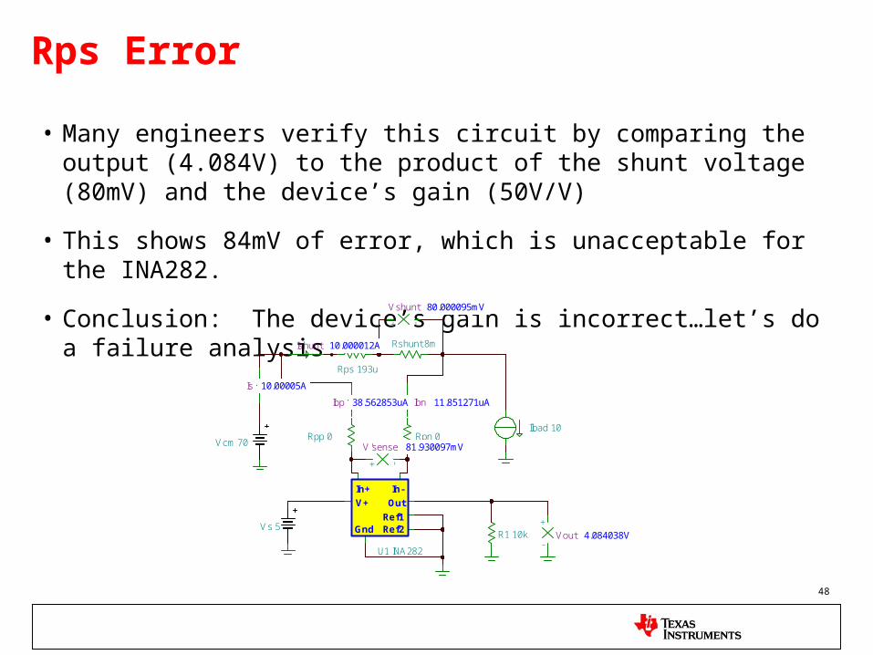
Rps Error
• Many engineers verify this circuit by comparing the output (4.084V) to the product of the shunt voltage (80mV) and the device’s gain (50V/V)
• This shows 84mV of error, which is unacceptable for the INA282.
• Conclusion: The device’s gain is incorrect…let’s do a failure analysis!
Vs 5R1 10k
-
+Vout
Rshunt 8m
V+
In+ In-
Out
Ref1Ref2Gnd
U1 INA282
Iload 10
Vcm 70
Rps 193u
Rpp 0 Rpn 0
-+
Vshunt
-+
V'sense
Ibp Ibn
Is
Ishunt 10.000012A
10.00005A
11.851271uA38.562853uA
81.930097mV
80.000095mV
4.084038V

49
Rps Error
• Not so fast!
• To determine error introduced by the device you must use V’sense
Vs 5R1 10k
-
+Vout
Rshunt 8m
V+
In+ In-
Out
Ref1Ref2Gnd
U1 INA282
Iload 10
Vcm 70
Rps 193u
Rpp 0 Rpn 0
-+
Vshunt
-+
V'sense
Ibp Ibn
Is
Ishunt 10.000012A
10.00005A
11.851271uA38.562853uA
81.930097mV
80.000095mV
4.084038V
Gain'VV senseidealout
idealout
idealoutmeasuredoutdevice V
VV100%e
%3.0
V
V50mV93.81
V
V50mV93.81V084.4
100(%)edevice
Not the device…no FA required.

50
PCB Layout & Troubleshooting Summary
• Always ensure that the shunt resistor is Kelvin-connected
• Make the input traces as short as possible
• Make the input traces as balanced as possible
• Place the current sensing device and shunt on the same side of the PCB
• To determine device error, look at voltage across device pins (Vsense)
• Check to see if device is within specification for given application– Quickly calculate error referred to output due to Vos, CMRR, and PSRR

Questions?
51
Additional Reading
• Current Sensing Fundamentals
• Current Sensing Devices
• Current Sensing Accuracy
• Current Sensing Layout & Troubleshooting
52
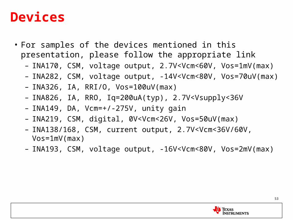
Devices
• For samples of the devices mentioned in this presentation, please follow the appropriate link– INA170, CSM, voltage output, 2.7V<Vcm<60V, Vos=1mV(max)
– INA282, CSM, voltage output, -14V<Vcm<80V, Vos=70uV(max)
– INA326, IA, RRI/O, Vos=100uV(max)
– INA826, IA, RRO, Iq=200uA(typ), 2.7V<Vsupply<36V
– INA149, DA, Vcm=+/-275V, unity gain
– INA219, CSM, digital, 0V<Vcm<26V, Vos=50uV(max)
– INA138/168, CSM, current output, 2.7V<Vcm<36V/60V, Vos=1mV(max)
– INA193, CSM, voltage output, -16V<Vcm<80V, Vos=2mV(max)
53

Backup
54
55
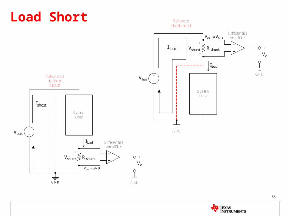
Load Short
SystemLoad
+
–busV
shuntR+
-
loadI
shuntV
GND
+
GND
+
-
oV
DifferentialAmplifier
GNDVcm
Rshunt not in short circuit
shortI
busV
SystemLoad
+
–
shuntR+
-
loadI
shuntV+
GND
+
-
oV
GND
DifferentialAmplifierbuscm VV
Rshunt in short circuit
shortI