Embed Size (px)
Citation preview
OpenVINO Starter Kit GT Edition User Manual December 17, 2019
www.terasic.com.cn
1
OpenVINO Starter Kit GT Edition User Manual December 17, 2019
www.terasic.com.cn
2
Content
Chapter 1 OpenVINO Stater Kit GT Edition .......................................... 4
1.1 Package Contents ........................................................................................................... 4
1.2 OpenVINO Starter Kit GT Edition System CD ............................................................. 5
1.3 Getting Help ................................................................................................................... 5
Chapter 2 Introduction of the OpenVINO Starter Kit GT Edition ..... 6
2.1 Layout and Components ................................................................................................ 6
2.2 Block Diagram of the OpenVINO Starter Kit GT Edition ............................................ 7
Chapter 3 Using the OpenVINO Starter Kit GT Edition ................... 10
3.1 Configuring the Cyclone V FPGA ............................................................................... 10
3.2 Board Status Elements ................................................................................................. 15
3.3 Clock Circuitry............................................................................................................. 16
3.4 Peripherals Connected to the FPGA ............................................................................ 16
3.4.1 User Push-buttons, Switches and LEDs ........................................................................ 16
3.4.2 7-Segment Displays ....................................................................................................... 19
3.4.3 SDRAM Memory .......................................................................................................... 21
3.4.4 DDR3 Memory .............................................................................................................. 22
3.4.5 UART to USB ............................................................................................................... 25
3.4.6 Arduino Uno R3 Expansion Header .............................................................................. 26
3.4.7 2x20 GPIO Expansion Header ...................................................................................... 31
Chapter 4 OpenVINO Starter Kit GT Edition System Builder ......... 37
4.1 Introduction .................................................................................................................. 37
4.2 General Design Flow ................................................................................................... 37
4.3 Using OpenVINO Starter Kit GT Edition System Builder .......................................... 38
Chapter 5 Examples of Advanced Demonstrations ........................... 44
5.1 OpenVINO Starter Kit GT Edition Factory Default Configuration ............................ 44
OpenVINO Starter Kit GT Edition User Manual December 17, 2019
www.terasic.com.cn
3
5.2 Nios II SDRAM Test.................................................................................................... 45
5.3 Verilog SDRAM Test ................................................................................................... 48
5.4 DDR3 SDRAM Test .................................................................................................... 50
5.5 DDR3 SDRAM Test by Nios II ................................................................................... 52
5.6 UART Control .............................................................................................................. 54
5.7 ADC Reading ............................................................................................................... 59
Chapter 6 Programming the EPCQ ...................................................... 64
6.1 Convert .sof File to .jic File ......................................................................................... 64
6.2 Write a .jic File to the EPCQ ....................................................................................... 67
6.3 Erase the EPCQ device ................................................................................................ 69
Chapter 7 PCIe Reference Design for Windows .................................. 70
7.1 PCI Express System Infrastructure .............................................................................. 70
7.2 PCI Express Software SDK ......................................................................................... 71
7.3 PCI Express Software Stack ........................................................................................ 71
7.4 PCIe Library API ......................................................................................................... 77
7.5 PCIe Reference Design - Fundamental ........................................................................ 81
7.6 PCIe Reference Design – DDR3.................................................................................. 86
Chapter 8 PCIe Reference Design for Linux .......................................... 93
8.1 PCI Express System Infrastructure .............................................................................. 93
8.2 PCI Express Software SDK ......................................................................................... 94
8.3 PCI Express Software Stack ........................................................................................ 94
8.4 PCI Express Library API ............................................................................................. 97
8.5 PCIe Reference Design – Fundamental ....................................................................... 97
8.6 PCIe Reference Design – DDR3................................................................................ 102
OpenVINO Starter Kit GT Edition User Manual December 17, 2019
www.terasic.com.cn
4
Chapter 1
OpenVINO Stater Kit GT Edition
The OpenVINO Starter Kit GT Edition presents a robust hardware design platform built
around the Intel Cyclone V FPGA, it also provides a powerful platform of reconfigurable
power with high performance and low power processing system. The OpenVINO Starter
Kit GT Edition is equipped with PCIe Gen2x4, high-speed DDR3 memory, GPIO, Arduino
and much more that promises many exciting applications.
The OpenVINO Starter Kit GT Edition is equipped with PCIe Gen2x4 interface, it is low
development cost, and can support users who develop mainstream applications and
OpenCL applications based on PCIe, as well as a wide range of high-speed connectivity
applications.
The OpenVINO Starter Kit GT Edition contains all the tools needed to use the board in
conjunction with a computer that runs the Microsoft Windows 7 or later.
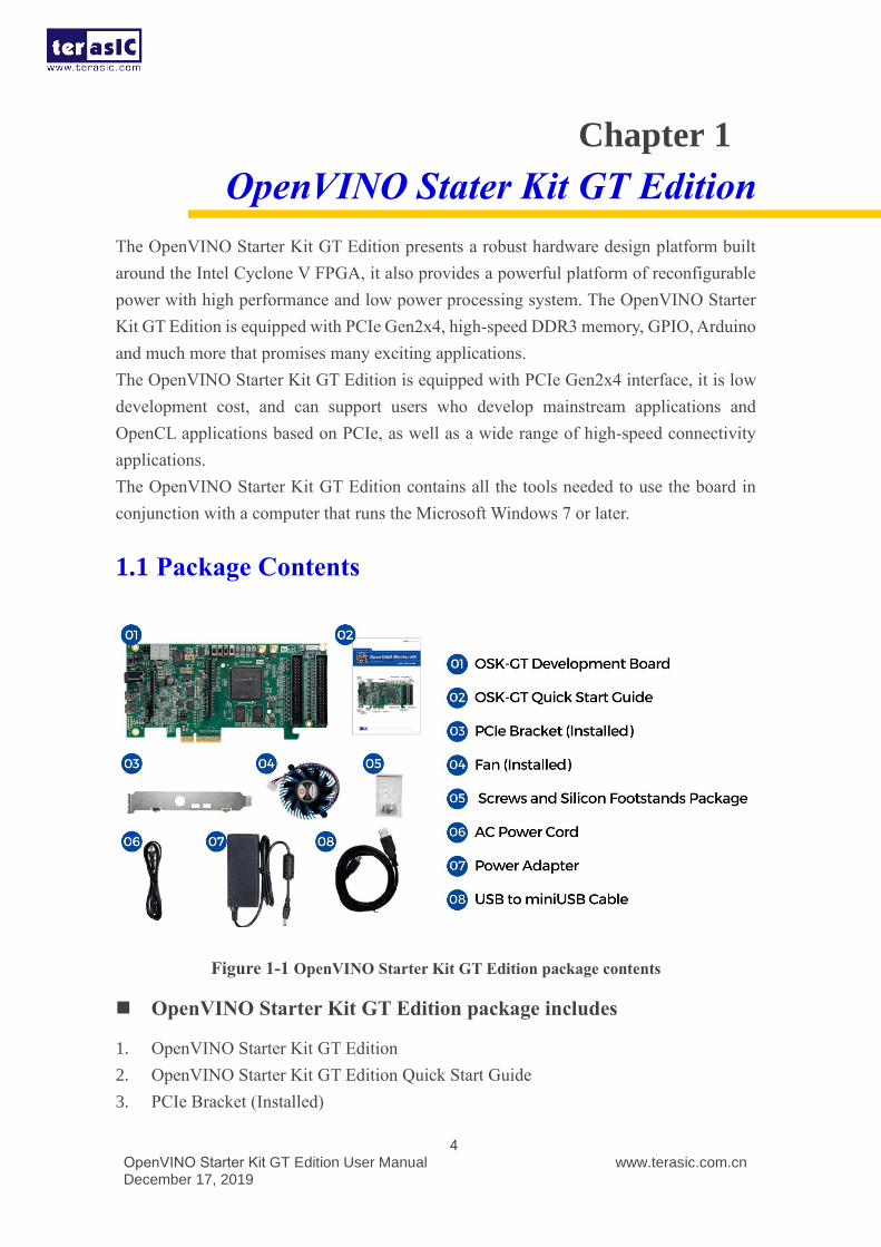
1.1 Package Contents
Figure 1-1 OpenVINO Starter Kit GT Edition package contents
◼ OpenVINO Starter Kit GT Edition package includes
1. OpenVINO Starter Kit GT Edition
2. OpenVINO Starter Kit GT Edition Quick Start Guide
3. PCIe Bracket (Installed)
OpenVINO Starter Kit GT Edition User Manual December 17, 2019
www.terasic.com.cn
5
4. Fan (Installed)
5. Screw and Silicon Footstands Package
6. AC Power Cord
7. Power Adapter
8. USB to mini-USB Cable
1.2 OpenVINO Starter Kit GT Edition System CD
The OpenVINO Starter Kit GT Edition System CD contains all the documents and
supporting materials associated with OpenVINO Starter Kit GT Edition, including the user
manual, system builder, reference designs, and device datasheets. Users can download this
system CD from the link http://OpenVINO Starter Kit.terasic.com/.
1.3 Getting Help
Here are the addresses where you can get help if you encounter any problems:
⚫ Terasic Inc.
⚫ 9F., No.176, Sec.2, Gongdao 5th Rd, East Dist, Hsinchu City, 30070. Taiwan
⚫ Email: [email protected]
⚫ Tel.: +886-3-575-0880
⚫ Website: http://OpenVINO Starter Kit.terasic.com/
OpenVINO Starter Kit GT Edition User Manual December 17, 2019
www.terasic.com.cn
6
Chapter 2
Introduction of the OpenVINO
Starter Kit GT Edition
This chapter provides an introduction to the features and design characteristics of the
OpenVINO Starter Kit GT Edition.
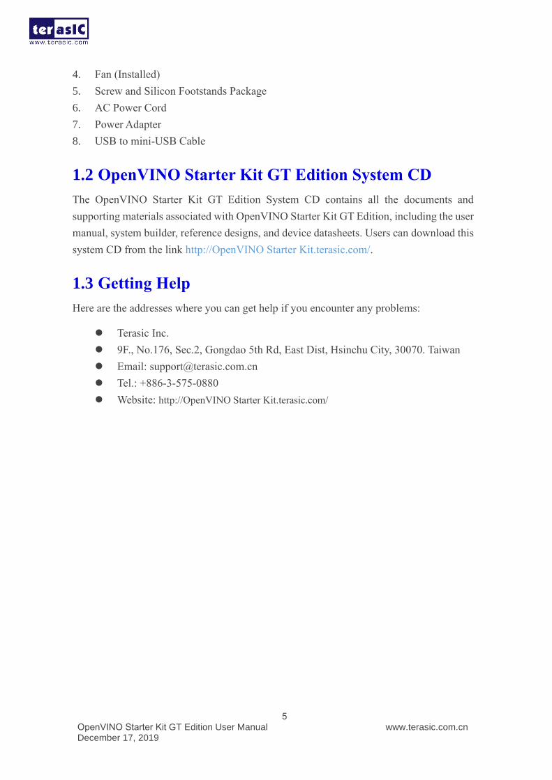
2.1 Layout and Components
Figure 2-1 and Figure 2-2 shows a photograph of the board. It depicts the layout of the
board and indicates the location of the connectors and key components.
Figure 2-1 OpenVINO Starter Kit GT Edition (top view)
OpenVINO Starter Kit GT Edition User Manual December 17, 2019
www.terasic.com.cn
7
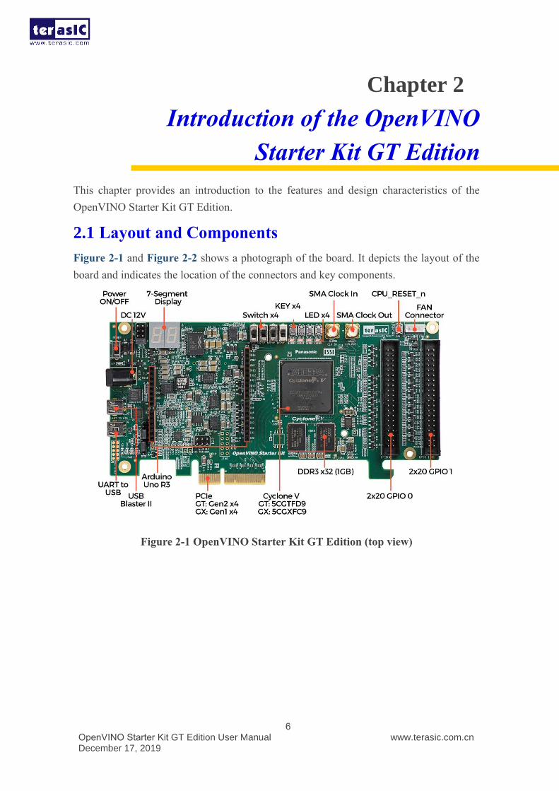
Figure 2-2 OpenVINO Starter Kit GT Edition (bottom view)
The OpenVINO Starter Kit GT Edition board has many features that allow users to
implement a wide range of designed circuits, from simple circuits to various multimedia
projects:
⚫ Intel FPGA Cyclone® V GT 5CGTFD9D5F27C7N device
⚫ Serial configuration device – EPCQ256
⚫ USB-Blaster II onboard for programming; JTAG Mode
⚫ UART to USB (USB Mini-B connector)
⚫ PCIe Gen2x4
⚫ 1GB DDR3 SDRAM (32-bit data bus)
⚫ 64MB SDRAM (16-bit data bus)
⚫ 4 push-buttons
⚫ 4 slide switches
⚫ 4 green LED
⚫ Two 7-segment displays
⚫ Four 50MHz clock sources from the clock generator
⚫ One Arduino header
⚫ Two 40 pin GPIO header
2.2 Block Diagram of the OpenVINO Starter Kit GT
Edition
Figure 2-3 is the block diagram of the board. All the connections are established through
the Cyclone V FPGA device to provide maximum flexibility for users. Users can configure
the FPGA to implement any system design.
OpenVINO Starter Kit GT Edition User Manual December 17, 2019
www.terasic.com.cn
8
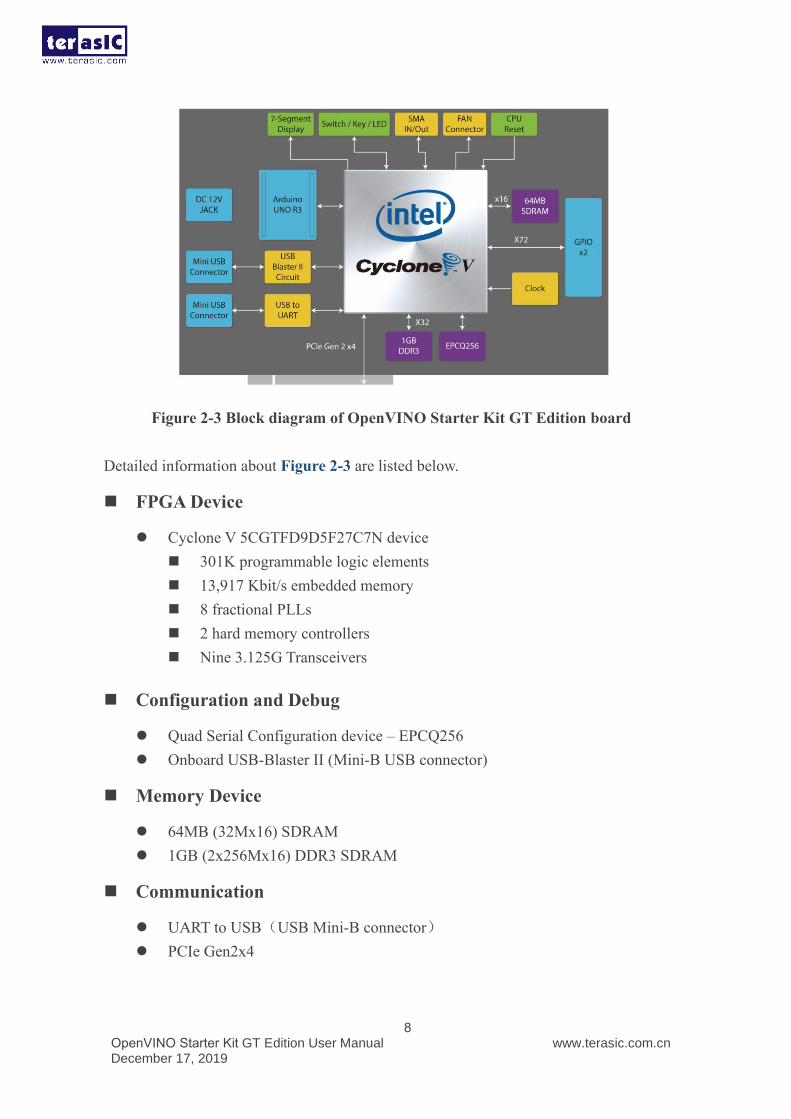
Figure 2-3 Block diagram of OpenVINO Starter Kit GT Edition board
Detailed information about Figure 2-3 are listed below.
◼ FPGA Device
⚫ Cyclone V 5CGTFD9D5F27C7N device
◼ 301K programmable logic elements
◼ 13,917 Kbit/s embedded memory
◼ 8 fractional PLLs
◼ 2 hard memory controllers
◼ Nine 3.125G Transceivers
◼ Configuration and Debug
⚫ Quad Serial Configuration device – EPCQ256
⚫ Onboard USB-Blaster II (Mini-B USB connector)
◼ Memory Device
⚫ 64MB (32Mx16) SDRAM
⚫ 1GB (2x256Mx16) DDR3 SDRAM
◼ Communication
⚫ UART to USB(USB Mini-B connector)
⚫ PCIe Gen2x4
OpenVINO Starter Kit GT Edition User Manual December 17, 2019
www.terasic.com.cn
9
◼ Connectors
⚫ Two 40 Pin GPIO header,features of each GPIO connector
◼ 36 General GPIO Pins
◼ Support to configureas 8 LVDS TX and LVDS RX
◼ With diode protection
◼ Configurable I/O standards (voltage levels: 3.3/2.5/1.8/1.5V)
⚫ One Arduino Uno Revision 3 header
◼ Analog ADC
◼ Interface: SPI
◼ Fast through put rate:500Ksps
◼ Channel number: 8
◼ Resolution: 12-bit
◼ Analog input range:0 ~ 4.096 V
◼ Digital IO
◼ With diode protection
⚫ SMA IN/OUT 3.3V Single-end input and output
◼ Switches/ Buttons/ Indicators
⚫ 5 user Keys (4 general keys, 1 CPU_RESET_n)
⚫ 4 user switches
⚫ 4 LEDG
⚫ Two 7-segment displays
◼ Power
⚫ 12V DC Input
⚫ PCIe 12V Input
◼ Cooling System
⚫ 12V Fan with 5000 Rotational Speed
OpenVINO Starter Kit GT Edition User Manual December 17, 2019
www.terasic.com.cn
10
Chapter 3
Using the OpenVINO Starter Kit GT
Edition
This chapter provides instructions to how to use the board and describes the peripherals.
3.1 Configuring the Cyclone V FPGA
There are two types of programming method supported by OpenVINO Starter Kit GT
Edition:
1. JTAG programming: It is named after the IEEE standards Joint Test Action Group.
The configuration bitstream is downloaded directly into the Cyclone V FPGA. The
FPGA will retain its current status as long as power is applied to the board; the
configuration information will be lost when the power is off.
2. AS programming: The other programming method is Active Serial configuration. The
configuration bitstream is downloaded into the Intel FPGA EPCQ256 device, which
provides non-volatile storage for the bit stream. The information is retained within
EPCQ256 even if the OpenVINO Starter Kit GT Edition board is turned off. When
the board is powered on, the configuration data in the EPCQ256 device is
automatically loaded into the Cyclone V FPGA.
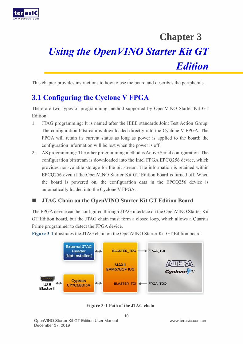
◼ JTAG Chain on the OpenVINO Starter Kit GT Edition Board
The FPGA device can be configured through JTAG interface on the OpenVINO Starter Kit
GT Edition board, but the JTAG chain must form a closed loop, which allows a Quartus
Prime programmer to detect the FPGA device.
Figure 3-1 illustrates the JTAG chain on the OpenVINO Starter Kit GT Edition board.
Figure 3-1 Path of the JTAG chain
OpenVINO Starter Kit GT Edition User Manual December 17, 2019
www.terasic.com.cn
11
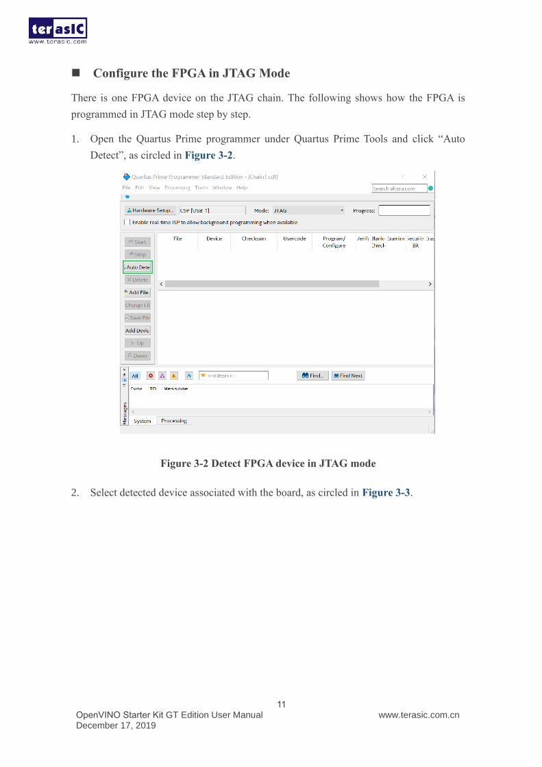
◼ Configure the FPGA in JTAG Mode
There is one FPGA device on the JTAG chain. The following shows how the FPGA is
programmed in JTAG mode step by step.
1. Open the Quartus Prime programmer under Quartus Prime Tools and click “Auto
Detect”, as circled in Figure 3-2.
Figure 3-2 Detect FPGA device in JTAG mode
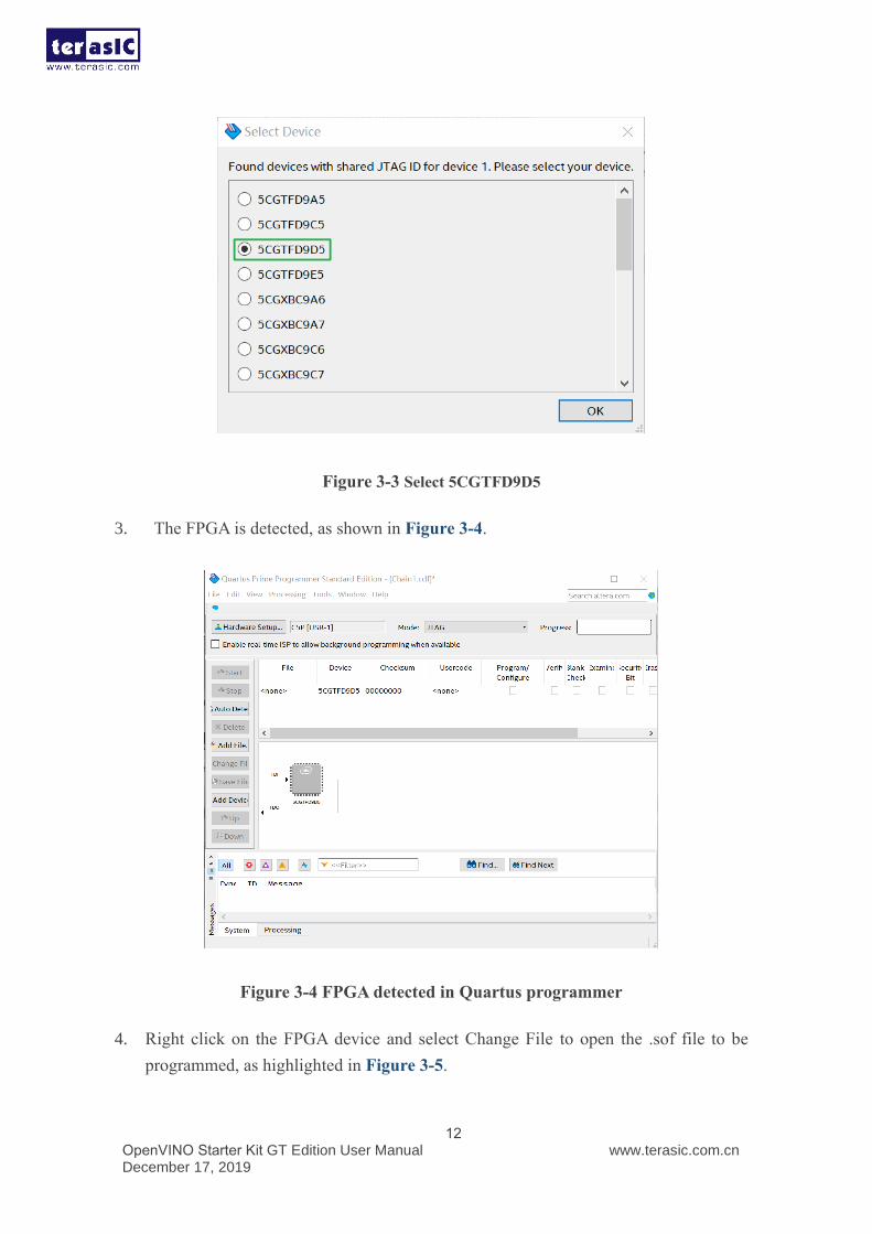
2. Select detected device associated with the board, as circled in Figure 3-3.
OpenVINO Starter Kit GT Edition User Manual December 17, 2019
www.terasic.com.cn
12
Figure 3-3 Select 5CGTFD9D5
3. The FPGA is detected, as shown in Figure 3-4.
Figure 3-4 FPGA detected in Quartus programmer
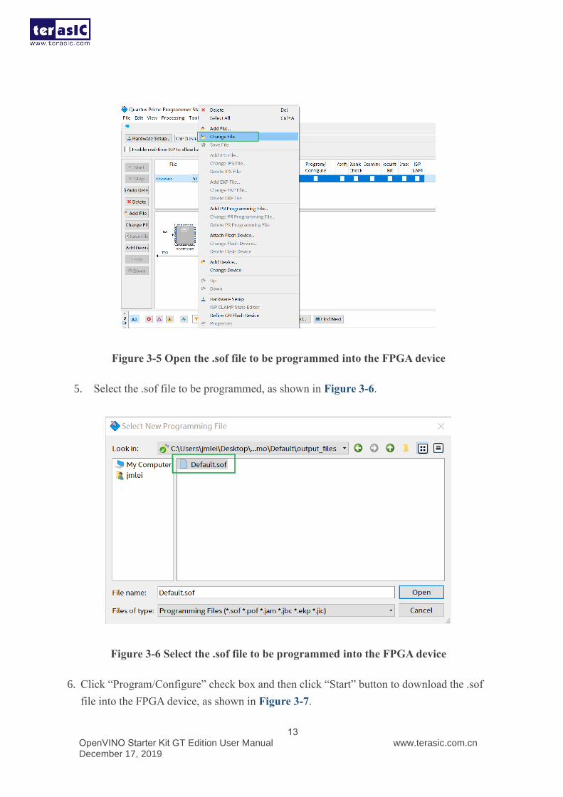
4. Right click on the FPGA device and select Change File to open the .sof file to be
programmed, as highlighted in Figure 3-5.
OpenVINO Starter Kit GT Edition User Manual December 17, 2019
www.terasic.com.cn
13
Figure 3-5 Open the .sof file to be programmed into the FPGA device
5. Select the .sof file to be programmed, as shown in Figure 3-6.
Figure 3-6 Select the .sof file to be programmed into the FPGA device
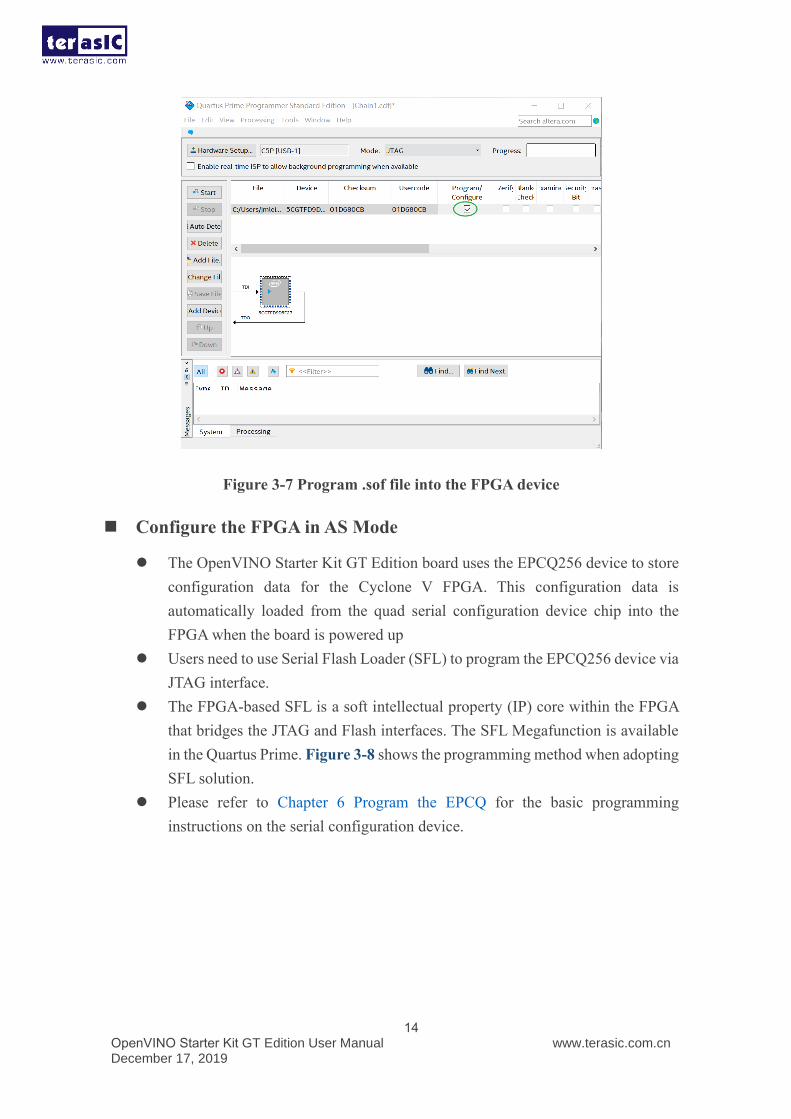
6. Click “Program/Configure” check box and then click “Start” button to download the .sof
file into the FPGA device, as shown in Figure 3-7.
OpenVINO Starter Kit GT Edition User Manual December 17, 2019
www.terasic.com.cn
14
Figure 3-7 Program .sof file into the FPGA device
◼ Configure the FPGA in AS Mode
⚫ The OpenVINO Starter Kit GT Edition board uses the EPCQ256 device to store
configuration data for the Cyclone V FPGA. This configuration data is
automatically loaded from the quad serial configuration device chip into the
FPGA when the board is powered up
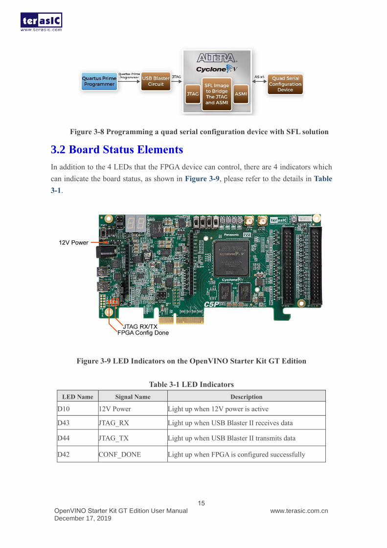
⚫ Users need to use Serial Flash Loader (SFL) to program the EPCQ256 device via
JTAG interface.
⚫ The FPGA-based SFL is a soft intellectual property (IP) core within the FPGA
that bridges the JTAG and Flash interfaces. The SFL Megafunction is available
in the Quartus Prime. Figure 3-8 shows the programming method when adopting
SFL solution.
⚫ Please refer to Chapter 6 Program the EPCQ for the basic programming
instructions on the serial configuration device.
OpenVINO Starter Kit GT Edition User Manual December 17, 2019
www.terasic.com.cn
15
Figure 3-8 Programming a quad serial configuration device with SFL solution
3.2 Board Status Elements
In addition to the 4 LEDs that the FPGA device can control, there are 4 indicators which
can indicate the board status, as shown in Figure 3-9, please refer to the details in Table
3-1.
Figure 3-9 LED Indicators on the OpenVINO Starter Kit GT Edition
Table 3-1 LED Indicators
LED Name Signal Name Description
D10 12V Power Light up when 12V power is active
D43 JTAG_RX Light up when USB Blaster II receives data
D44 JTAG_TX Light up when USB Blaster II transmits data
D42 CONF_DONE Light up when FPGA is configured successfully
OpenVINO Starter Kit GT Edition User Manual December 17, 2019
www.terasic.com.cn
16
3.3 Clock Circuitry
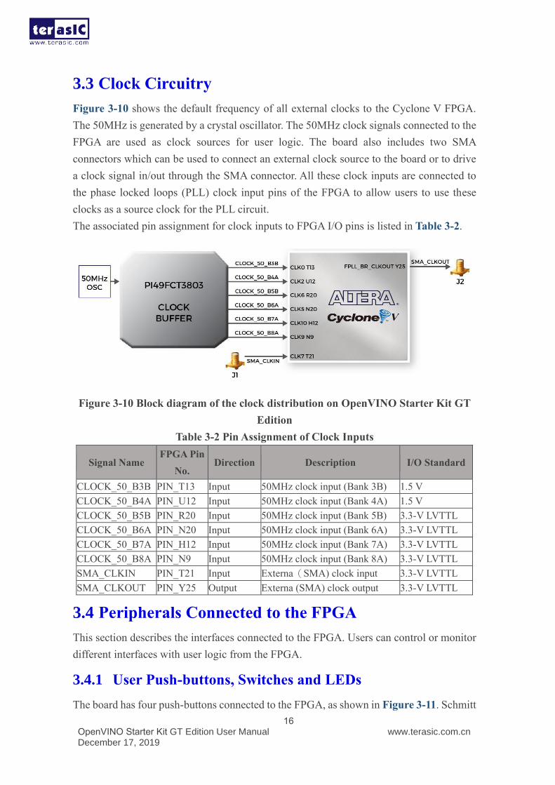
Figure 3-10 shows the default frequency of all external clocks to the Cyclone V FPGA.
The 50MHz is generated by a crystal oscillator. The 50MHz clock signals connected to the
FPGA are used as clock sources for user logic. The board also includes two SMA
connectors which can be used to connect an external clock source to the board or to drive
a clock signal in/out through the SMA connector. All these clock inputs are connected to
the phase locked loops (PLL) clock input pins of the FPGA to allow users to use these
clocks as a source clock for the PLL circuit.
The associated pin assignment for clock inputs to FPGA I/O pins is listed in Table 3-2.
Figure 3-10 Block diagram of the clock distribution on OpenVINO Starter Kit GT
Edition
Table 3-2 Pin Assignment of Clock Inputs
Signal Name FPGA Pin
No. Direction Description I/O Standard
CLOCK_50_B3B PIN_T13 Input 50MHz clock input (Bank 3B) 1.5 V
CLOCK_50_B4A PIN_U12 Input 50MHz clock input (Bank 4A) 1.5 V
CLOCK_50_B5B PIN_R20 Input 50MHz clock input (Bank 5B) 3.3-V LVTTL
CLOCK_50_B6A PIN_N20 Input 50MHz clock input (Bank 6A) 3.3-V LVTTL
CLOCK_50_B7A PIN_H12 Input 50MHz clock input (Bank 7A) 3.3-V LVTTL
CLOCK_50_B8A PIN_N9 Input 50MHz clock input (Bank 8A) 3.3-V LVTTL
SMA_CLKIN PIN_T21 Input Externa(SMA) clock input 3.3-V LVTTL
SMA_CLKOUT PIN_Y25 Output Externa (SMA) clock output 3.3-V LVTTL
3.4 Peripherals Connected to the FPGA
This section describes the interfaces connected to the FPGA. Users can control or monitor
different interfaces with user logic from the FPGA.
3.4.1 User Push-buttons, Switches and LEDs
The board has four push-buttons connected to the FPGA, as shown in Figure 3-11. Schmitt
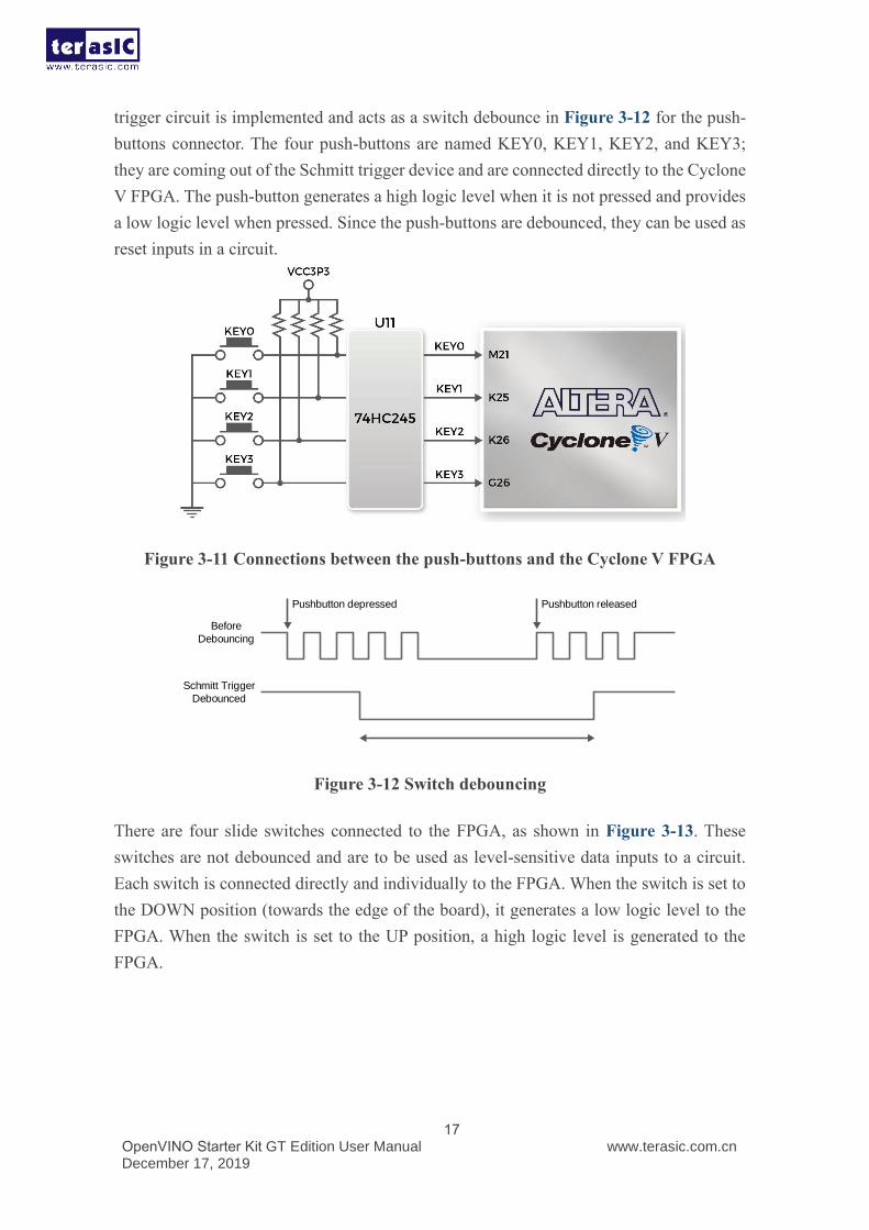
OpenVINO Starter Kit GT Edition User Manual December 17, 2019
www.terasic.com.cn
17
trigger circuit is implemented and acts as a switch debounce in Figure 3-12 for the push-
buttons connector. The four push-buttons are named KEY0, KEY1, KEY2, and KEY3;
they are coming out of the Schmitt trigger device and are connected directly to the Cyclone
V FPGA. The push-button generates a high logic level when it is not pressed and provides
a low logic level when pressed. Since the push-buttons are debounced, they can be used as
reset inputs in a circuit.
Figure 3-11 Connections between the push-buttons and the Cyclone V FPGA
Figure 3-12 Switch debouncing
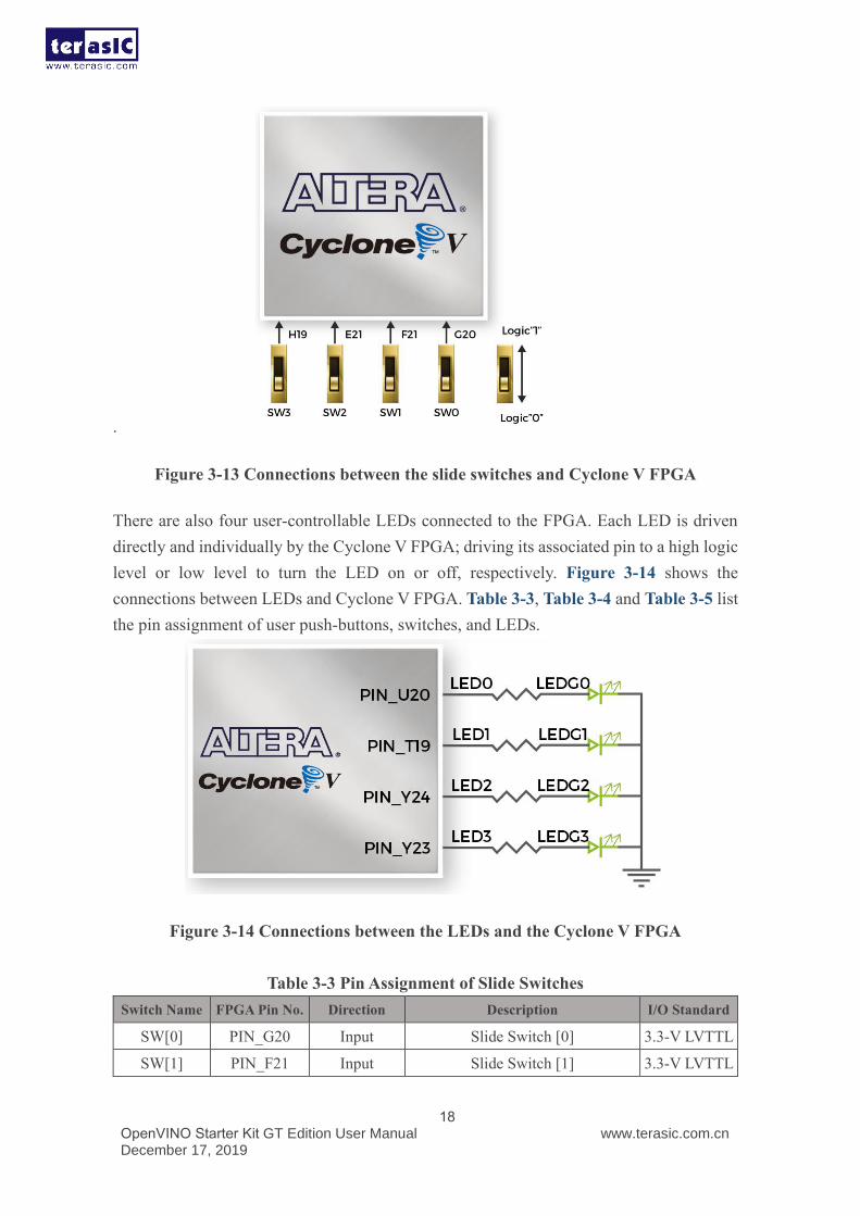
There are four slide switches connected to the FPGA, as shown in Figure 3-13. These
switches are not debounced and are to be used as level-sensitive data inputs to a circuit.
Each switch is connected directly and individually to the FPGA. When the switch is set to
the DOWN position (towards the edge of the board), it generates a low logic level to the
FPGA. When the switch is set to the UP position, a high logic level is generated to the
FPGA.
Pushbutton releasedPushbutton depressed
Before
Debouncing
Schmitt Trigger
Debounced
OpenVINO Starter Kit GT Edition User Manual December 17, 2019
www.terasic.com.cn
18
.
Figure 3-13 Connections between the slide switches and Cyclone V FPGA
There are also four user-controllable LEDs connected to the FPGA. Each LED is driven
directly and individually by the Cyclone V FPGA; driving its associated pin to a high logic
level or low level to turn the LED on or off, respectively. Figure 3-14 shows the
connections between LEDs and Cyclone V FPGA. Table 3-3, Table 3-4 and Table 3-5 list
the pin assignment of user push-buttons, switches, and LEDs.
Figure 3-14 Connections between the LEDs and the Cyclone V FPGA
Table 3-3 Pin Assignment of Slide Switches
Switch Name FPGA Pin No. Direction Description I/O Standard
SW[0] PIN_G20 Input Slide Switch [0] 3.3-V LVTTL
SW[1] PIN_F21 Input Slide Switch [1] 3.3-V LVTTL
OpenVINO Starter Kit GT Edition User Manual December 17, 2019
www.terasic.com.cn
19
SW[2] PIN_E21 Input Slide Switch [2] 3.3-V LVTTL
SW[3] PIN_H19 Input Slide Switch [3] 3.3-V LVTTL
Table 3-4 Pin Assignment of Push-buttons
Key Name FPGA Pin No. Direction Description I/O
Standard
CPU_RESET_n PIN_AB24 Input
Generate a high logic level when it
is not pressed
3.3-V
LVTTL
KEY[0] PIN_M21 Input
Generate a high logic level when it
is not pressed. Four push-buttons
(KEY0, KEY1, KEY2 and KEY3)
are debounced.
3.3-V
LVTTL
KEY[1] PIN_K25 Input 3.3-V
LVTTL
KEY[2] PIN_K26 Input 3.3-V
LVTTL
KEY[3] PIN_G26 Input 3.3-V
LVTTL
Table 3-5 LED Pin Assignment of LEDs
LED
Name FPGA Pin No. Direction Description
I/O
Standard
LED[0] PIN_U20 Output
Drive high logic 1 to I/O pin to turn
the LED on.
Drive lowh logic 0 to I/O pin to turn
the LED off.
3.3-V
LVTTL
LED[1] PIN_T19 Output 3.3-V
LVTTL
LED[2] PIN_Y24 Output 3.3-V
LVTTL
LED[3] PIN_Y23 Output 3.3-V
LVTTL
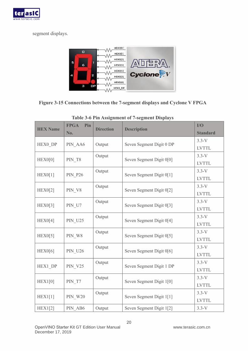
3.4.2 7-Segment Displays
OpenVINO Starter Kit GT Edition has two 7-segment displays. Figure 3-15 shows the
connection of seven segments (common anode) to pins on Cyclone V FPGA.The segment
can be turned on or off by applying a low logic level or high logic level from the FPGA,
respectively. Each segment in a display is indexed from 0 to 6, with the corresponding
positions given in the Figure 3-15. Table 3-6 shows the pin assignment of FPGA to the 7-
OpenVINO Starter Kit GT Edition User Manual December 17, 2019
www.terasic.com.cn
20
segment displays.
Figure 3-15 Connections between the 7-segment displays and Cyclone V FPGA
Table 3-6 Pin Assignment of 7-segment Displays
HEX Name FPGA Pin
No. Direction Description
I/O
Standard
HEX0_DP PIN_AA6 Output Seven Segment Digit 0 DP 3.3-V
LVTTL
HEX0[0] PIN_T8 Output
Seven Segment Digit 0[0] 3.3-V
LVTTL
HEX0[1] PIN_P26 Output
Seven Segment Digit 0[1] 3.3-V
LVTTL
HEX0[2] PIN_V8 Output
Seven Segment Digit 0[2] 3.3-V
LVTTL
HEX0[3] PIN_U7 Output
Seven Segment Digit 0[3] 3.3-V
LVTTL
HEX0[4] PIN_U25 Output
Seven Segment Digit 0[4] 3.3-V
LVTTL
HEX0[5] PIN_W8 Output
Seven Segment Digit 0[5] 3.3-V
LVTTL
HEX0[6] PIN_U26 Output
Seven Segment Digit 0[6] 3.3-V
LVTTL
HEX1_DP PIN_V25 Output
Seven Segment Digit 1 DP 3.3-V
LVTTL
HEX1[0] PIN_T7 Output
Seven Segment Digit 1[0] 3.3-V
LVTTL
HEX1[1] PIN_W20 Output
Seven Segment Digit 1[1] 3.3-V
LVTTL
HEX1[2] PIN_AB6 Output Seven Segment Digit 1[2] 3.3-V
OpenVINO Starter Kit GT Edition User Manual December 17, 2019
www.terasic.com.cn
21
LVTTL
HEX1[3] PIN_AC22 Output
Seven Segment Digit 1[3] 3.3-V
LVTTL
HEX1[4] PIN_Y9 Output
Seven Segment Digit 1[4] 3.3-V
LVTTL
HEX1[5] PIN_W21 Output
Seven Segment Digit 1[5] 3.3-V
LVTTL
HEX1[6] PIN_N25 Output
Seven Segment Digit 1[6] 3.3-V
LVTTL
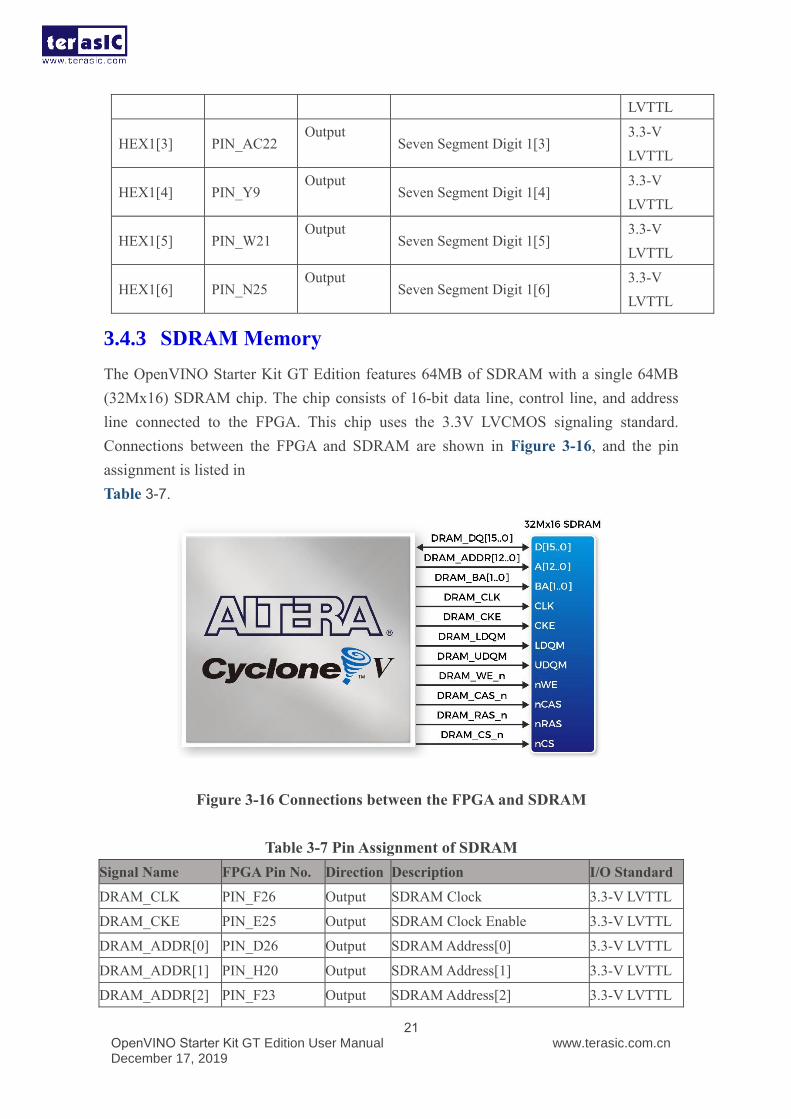
3.4.3 SDRAM Memory
The OpenVINO Starter Kit GT Edition features 64MB of SDRAM with a single 64MB
(32Mx16) SDRAM chip. The chip consists of 16-bit data line, control line, and address
line connected to the FPGA. This chip uses the 3.3V LVCMOS signaling standard.
Connections between the FPGA and SDRAM are shown in Figure 3-16, and the pin
assignment is listed in
Table 3-7.
Figure 3-16 Connections between the FPGA and SDRAM
Table 3-7 Pin Assignment of SDRAM
Signal Name FPGA Pin No. Direction Description I/O Standard
DRAM_CLK PIN_F26 Output SDRAM Clock 3.3-V LVTTL
DRAM_CKE PIN_E25 Output SDRAM Clock Enable 3.3-V LVTTL
DRAM_ADDR[0] PIN_D26 Output SDRAM Address[0] 3.3-V LVTTL
DRAM_ADDR[1] PIN_H20 Output SDRAM Address[1] 3.3-V LVTTL
DRAM_ADDR[2] PIN_F23 Output SDRAM Address[2] 3.3-V LVTTL
OpenVINO Starter Kit GT Edition User Manual December 17, 2019
www.terasic.com.cn
22
DRAM_ADDR[3] PIN_G22 Output SDRAM Address[3] 3.3-V LVTTL
DRAM_ADDR[4] PIN_B25 Output SDRAM Address[4] 3.3-V LVTTL
DRAM_ADDR[5] PIN_D22 Output SDRAM Address[5] 3.3-V LVTTL
DRAM_ADDR[6] PIN_C25 Output SDRAM Address[6] 3.3-V LVTTL
DRAM_ADDR[7] PIN_E23 Output SDRAM Address[7] 3.3-V LVTTL
DRAM_ADDR[8] PIN_B26 Output SDRAM Address[8] 3.3-V LVTTL
DRAM_ADDR[9] PIN_E24 Output SDRAM Address[9] 3.3-V LVTTL
DRAM_ADDR[10] PIN_D25 Output SDRAM Address[10] 3.3-V LVTTL
DRAM_ADDR[11] PIN_M26 Output SDRAM Address[11] 3.3-V LVTTL
DRAM_ADDR[12] PIN_M25 Output SDRAM Address[12] 3.3-V LVTTL
DRAM_BA[0] PIN_J20 Output SDRAM Bank Address[0] 3.3-V LVTTL
DRAM_BA[1] PIN_H22 Output SDRAM Bank Address[1] 3.3-V LVTTL
DRAM_DQ[0] PIN_L24 Inout SDRAM Data[0] 3.3-V LVTTL
DRAM_DQ[1] PIN_M24 Inout SDRAM Data[1] 3.3-V LVTTL
DRAM_DQ[2] PIN_N23 Inout SDRAM Data[2] 3.3-V LVTTL
DRAM_DQ[3] PIN_K23 Inout SDRAM Data[3] 3.3-V LVTTL
DRAM_DQ[4] PIN_H24 Inout SDRAM Data[4] 3.3-V LVTTL
DRAM_DQ[5] PIN_J23 Inout SDRAM Data[5] 3.3-V LVTTL
DRAM_DQ[6] PIN_K24 Inout SDRAM Data[6] 3.3-V LVTTL
DRAM_DQ[7] PIN_L22 Inout SDRAM Data[7] 3.3-V LVTTL
DRAM_DQ[8] PIN_G25 Inout SDRAM Data[8] 3.3-V LVTTL
DRAM_DQ[9] PIN_G24 Inout SDRAM Data[9] 3.3-V LVTTL
DRAM_DQ[10] PIN_H25 Inout SDRAM Data[10] 3.3-V LVTTL
DRAM_DQ[11] PIN_J21 Inout SDRAM Data[11] 3.3-V LVTTL
DRAM_DQ[12] PIN_L23 Inout SDRAM Data[12] 3.3-V LVTTL
DRAM_DQ[13] PIN_K21 Inout SDRAM Data[13] 3.3-V LVTTL
DRAM_DQ[14] PIN_N24 Inout SDRAM Data[14] 3.3-V LVTTL
DRAM_DQ[15] PIN_M22 Inout SDRAM Data[15] 3.3-V LVTTL
DRAM_LDQM PIN_H23 Output DQ[7:0] SDRAM Data Mask 3.3-V LVTTL
DRAM_UDQM PIN_F24 Output DQ[15:8] SDRAM Data Mask 3.3-V LVTTL
DRAM_CS_n PIN_F22 Output SDRAM Chip Select 3.3-V LVTTL
DRAM_WE_n PIN_J25 Output SDRAM Write Enable 3.3-V LVTTL
DRAM_CAS_n PIN_J26 Output SDRAM Column Address Strobe 3.3-V LVTTL
DRAM_RAS_n PIN_E26 Output SDRAM Row Address Strobe 3.3-V LVTTL
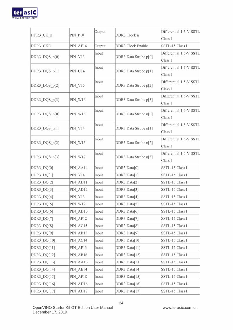
3.4.4 DDR3 Memory
OpenVINO Starter Kit GT Edition supports 1GB of DDR3 SDRAM comprising of two
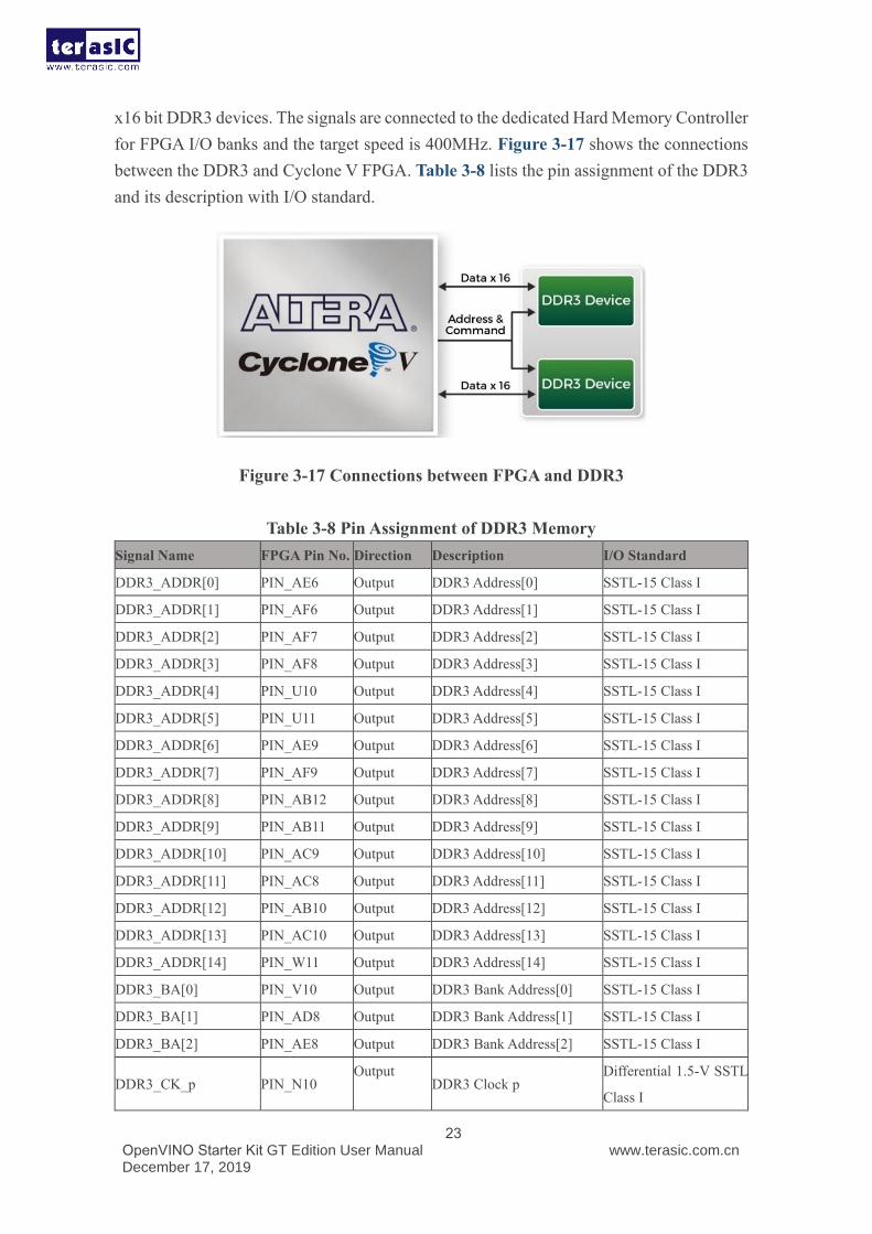
OpenVINO Starter Kit GT Edition User Manual December 17, 2019
www.terasic.com.cn
23
x16 bit DDR3 devices. The signals are connected to the dedicated Hard Memory Controller
for FPGA I/O banks and the target speed is 400MHz. Figure 3-17 shows the connections
between the DDR3 and Cyclone V FPGA. Table 3-8 lists the pin assignment of the DDR3
and its description with I/O standard.
Figure 3-17 Connections between FPGA and DDR3
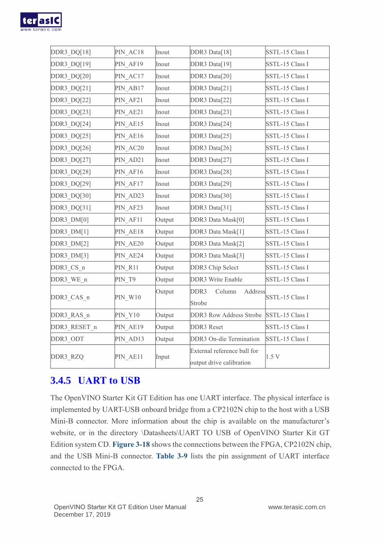
Table 3-8 Pin Assignment of DDR3 Memory
Signal Name FPGA Pin No. Direction Description I/O Standard
DDR3_ADDR[0] PIN_AE6 Output DDR3 Address[0] SSTL-15 Class I
DDR3_ADDR[1] PIN_AF6 Output DDR3 Address[1] SSTL-15 Class I
DDR3_ADDR[2] PIN_AF7 Output DDR3 Address[2] SSTL-15 Class I
DDR3_ADDR[3] PIN_AF8 Output DDR3 Address[3] SSTL-15 Class I
DDR3_ADDR[4] PIN_U10 Output DDR3 Address[4] SSTL-15 Class I
DDR3_ADDR[5] PIN_U11 Output DDR3 Address[5] SSTL-15 Class I
DDR3_ADDR[6] PIN_AE9 Output DDR3 Address[6] SSTL-15 Class I
DDR3_ADDR[7] PIN_AF9 Output DDR3 Address[7] SSTL-15 Class I
DDR3_ADDR[8] PIN_AB12 Output DDR3 Address[8] SSTL-15 Class I
DDR3_ADDR[9] PIN_AB11 Output DDR3 Address[9] SSTL-15 Class I
DDR3_ADDR[10] PIN_AC9 Output DDR3 Address[10] SSTL-15 Class I
DDR3_ADDR[11] PIN_AC8 Output DDR3 Address[11] SSTL-15 Class I
DDR3_ADDR[12] PIN_AB10 Output DDR3 Address[12] SSTL-15 Class I
DDR3_ADDR[13] PIN_AC10 Output DDR3 Address[13] SSTL-15 Class I
DDR3_ADDR[14] PIN_W11 Output DDR3 Address[14] SSTL-15 Class I
DDR3_BA[0] PIN_V10 Output DDR3 Bank Address[0] SSTL-15 Class I
DDR3_BA[1] PIN_AD8 Output DDR3 Bank Address[1] SSTL-15 Class I
DDR3_BA[2] PIN_AE8 Output DDR3 Bank Address[2] SSTL-15 Class I
DDR3_CK_p PIN_N10 Output
DDR3 Clock p Differential 1.5-V SSTL
Class I
OpenVINO Starter Kit GT Edition User Manual December 17, 2019
www.terasic.com.cn
24
DDR3_CK_n PIN_P10 Output
DDR3 Clock n Differential 1.5-V SSTL
Class I
DDR3_CKE PIN_AF14 Output DDR3 Clock Enable SSTL-15 Class I
DDR3_DQS_p[0] PIN_V13 Inout
DDR3 Data Strobe p[0] Differential 1.5-V SSTL
Class I
DDR3_DQS_p[1] PIN_U14 Inout
DDR3 Data Strobe p[1] Differential 1.5-V SSTL
Class I
DDR3_DQS_p[2] PIN_V15 Inout
DDR3 Data Strobe p[2] Differential 1.5-V SSTL
Class I
DDR3_DQS_p[3] PIN_W16 Inout
DDR3 Data Strobe p[3] Differential 1.5-V SSTL
Class I
DDR3_DQS_n[0] PIN_W13 Inout
DDR3 Data Strobe n[0] Differential 1.5-V SSTL
Class I
DDR3_DQS_n[1] PIN_V14 Inout
DDR3 Data Strobe n[1] Differential 1.5-V SSTL
Class I
DDR3_DQS_n[2] PIN_W15 Inout
DDR3 Data Strobe n[2] Differential 1.5-V SSTL
Class I
DDR3_DQS_n[3] PIN_W17 Inout
DDR3 Data Strobe n[3] Differential 1.5-V SSTL
Class I
DDR3_DQ[0] PIN_AA14 Inout DDR3 Data[0] SSTL-15 Class I
DDR3_DQ[1] PIN_Y14 Inout DDR3 Data[1] SSTL-15 Class I
DDR3_DQ[2] PIN_AD11 Inout DDR3 Data[2] SSTL-15 Class I
DDR3_DQ[3] PIN_AD12 Inout DDR3 Data[3] SSTL-15 Class I
DDR3_DQ[4] PIN_Y13 Inout DDR3 Data[4] SSTL-15 Class I
DDR3_DQ[5] PIN_W12 Inout DDR3 Data[5] SSTL-15 Class I
DDR3_DQ[6] PIN_AD10 Inout DDR3 Data[6] SSTL-15 Class I
DDR3_DQ[7] PIN_AF12 Inout DDR3 Data[7] SSTL-15 Class I
DDR3_DQ[8] PIN_AC15 Inout DDR3 Data[8] SSTL-15 Class I
DDR3_DQ[9] PIN_AB15 Inout DDR3 Data[9] SSTL-15 Class I
DDR3_DQ[10] PIN_AC14 Inout DDR3 Data[10] SSTL-15 Class I
DDR3_DQ[11] PIN_AF13 Inout DDR3 Data[11] SSTL-15 Class I
DDR3_DQ[12] PIN_AB16 Inout DDR3 Data[12] SSTL-15 Class I
DDR3_DQ[13] PIN_AA16 Inout DDR3 Data[13] SSTL-15 Class I
DDR3_DQ[14] PIN_AE14 Inout DDR3 Data[14] SSTL-15 Class I
DDR3_DQ[15] PIN_AF18 Inout DDR3 Data[15] SSTL-15 Class I
DDR3_DQ[16] PIN_AD16 Inout DDR3 Data[16] SSTL-15 Class I
DDR3_DQ[17] PIN_AD17 Inout DDR3 Data[17] SSTL-15 Class I
OpenVINO Starter Kit GT Edition User Manual December 17, 2019
www.terasic.com.cn
25
DDR3_DQ[18] PIN_AC18 Inout DDR3 Data[18] SSTL-15 Class I
DDR3_DQ[19] PIN_AF19 Inout DDR3 Data[19] SSTL-15 Class I
DDR3_DQ[20] PIN_AC17 Inout DDR3 Data[20] SSTL-15 Class I
DDR3_DQ[21] PIN_AB17 Inout DDR3 Data[21] SSTL-15 Class I
DDR3_DQ[22] PIN_AF21 Inout DDR3 Data[22] SSTL-15 Class I
DDR3_DQ[23] PIN_AE21 Inout DDR3 Data[23] SSTL-15 Class I
DDR3_DQ[24] PIN_AE15 Inout DDR3 Data[24] SSTL-15 Class I
DDR3_DQ[25] PIN_AE16 Inout DDR3 Data[25] SSTL-15 Class I
DDR3_DQ[26] PIN_AC20 Inout DDR3 Data[26] SSTL-15 Class I
DDR3_DQ[27] PIN_AD21 Inout DDR3 Data[27] SSTL-15 Class I
DDR3_DQ[28] PIN_AF16 Inout DDR3 Data[28] SSTL-15 Class I
DDR3_DQ[29] PIN_AF17 Inout DDR3 Data[29] SSTL-15 Class I
DDR3_DQ[30] PIN_AD23 Inout DDR3 Data[30] SSTL-15 Class I
DDR3_DQ[31] PIN_AF23 Inout DDR3 Data[31] SSTL-15 Class I
DDR3_DM[0] PIN_AF11 Output DDR3 Data Mask[0] SSTL-15 Class I
DDR3_DM[1] PIN_AE18 Output DDR3 Data Mask[1] SSTL-15 Class I
DDR3_DM[2] PIN_AE20 Output DDR3 Data Mask[2] SSTL-15 Class I
DDR3_DM[3] PIN_AE24 Output DDR3 Data Mask[3] SSTL-15 Class I
DDR3_CS_n PIN_R11 Output DDR3 Chip Select SSTL-15 Class I
DDR3_WE_n PIN_T9 Output DDR3 Write Enable SSTL-15 Class I
DDR3_CAS_n PIN_W10 Output DDR3 Column Address
Strobe SSTL-15 Class I
DDR3_RAS_n PIN_Y10 Output DDR3 Row Address Strobe SSTL-15 Class I
DDR3_RESET_n PIN_AE19 Output DDR3 Reset SSTL-15 Class I
DDR3_ODT PIN_AD13 Output DDR3 On-die Termination SSTL-15 Class I
DDR3_RZQ PIN_AE11 Input External reference ball for
output drive calibration 1.5 V
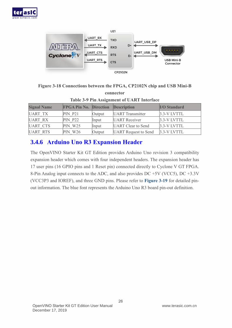
3.4.5 UART to USB
The OpenVINO Starter Kit GT Edition has one UART interface. The physical interface is
implemented by UART-USB onboard bridge from a CP2102N chip to the host with a USB
Mini-B connector. More information about the chip is available on the manufacturer’s
website, or in the directory \Datasheets\UART TO USB of OpenVINO Starter Kit GT
Edition system CD. Figure 3-18 shows the connections between the FPGA, CP2102N chip,
and the USB Mini-B connector. Table 3-9 lists the pin assignment of UART interface
connected to the FPGA.
OpenVINO Starter Kit GT Edition User Manual December 17, 2019
www.terasic.com.cn
26
Figure 3-18 Connections between the FPGA, CP2102N chip and USB Mini-B
connector
Table 3-9 Pin Assignment of UART Interface
Signal Name FPGA Pin No. Direction Description I/O Standard
UART_TX PIN_P21 Output UART Transmitter 3.3-V LVTTL
UART_RX PIN_P22 Input UART Receiver 3.3-V LVTTL
UART_CTS PIN_W25 Input UART Clear to Send 3.3-V LVTTL
UART_RTS PIN_W26 Output UART Request to Send 3.3-V LVTTL
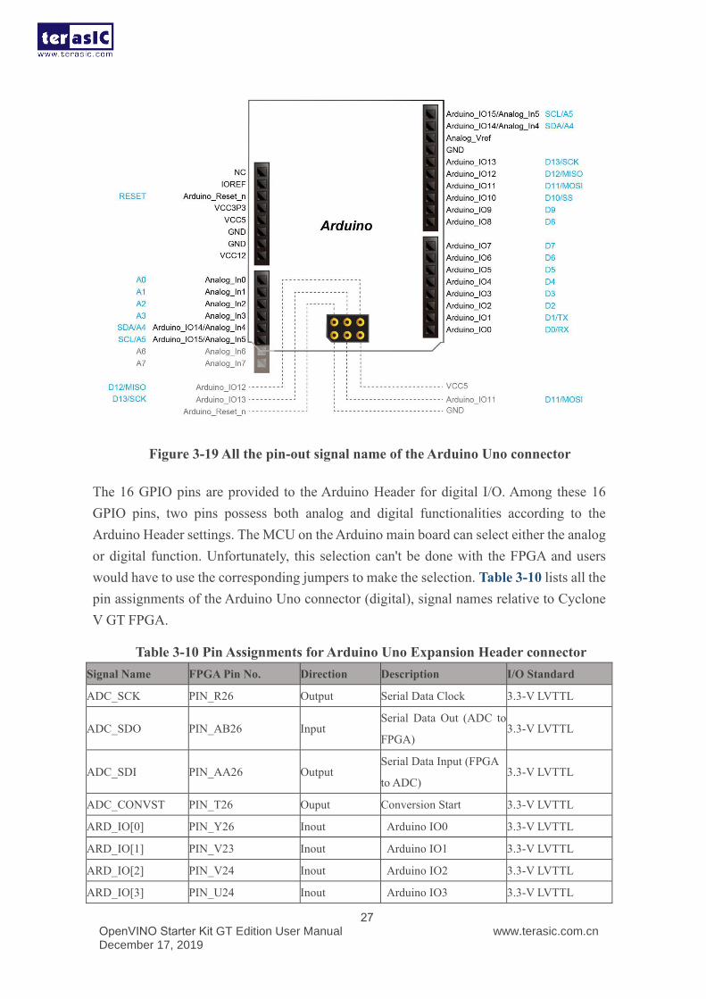
3.4.6 Arduino Uno R3 Expansion Header
The OpenVINO Starter Kit GT Edition provides Arduino Uno revision 3 compatibility
expansion header which comes with four independent headers. The expansion header has
17 user pins (16 GPIO pins and 1 Reset pin) connected directly to Cyclone V GT FPGA.
8-Pin Analog input connects to the ADC, and also provides DC +5V (VCC5), DC +3.3V
(VCC3P3 and IOREF), and three GND pins. Please refer to Figure 3-19 for detailed pin-
out information. The blue font represents the Arduino Uno R3 board pin-out definition.
OpenVINO Starter Kit GT Edition User Manual December 17, 2019
www.terasic.com.cn
27
Figure 3-19 All the pin-out signal name of the Arduino Uno connector
The 16 GPIO pins are provided to the Arduino Header for digital I/O. Among these 16
GPIO pins, two pins possess both analog and digital functionalities according to the
Arduino Header settings. The MCU on the Arduino main board can select either the analog
or digital function. Unfortunately, this selection can't be done with the FPGA and users
would have to use the corresponding jumpers to make the selection. Table 3-10 lists all the
pin assignments of the Arduino Uno connector (digital), signal names relative to Cyclone
V GT FPGA.
Table 3-10 Pin Assignments for Arduino Uno Expansion Header connector
Signal Name FPGA Pin No. Direction Description I/O Standard
ADC_SCK PIN_R26 Output Serial Data Clock 3.3-V LVTTL
ADC_SDO PIN_AB26 Input Serial Data Out (ADC to
FPGA) 3.3-V LVTTL
ADC_SDI PIN_AA26 Output Serial Data Input (FPGA
to ADC) 3.3-V LVTTL
ADC_CONVST PIN_T26 Ouput Conversion Start 3.3-V LVTTL
ARD_IO[0] PIN_Y26 Inout Arduino IO0 3.3-V LVTTL
ARD_IO[1] PIN_V23 Inout Arduino IO1 3.3-V LVTTL
ARD_IO[2] PIN_V24 Inout Arduino IO2 3.3-V LVTTL
ARD_IO[3] PIN_U24 Inout Arduino IO3 3.3-V LVTTL
OpenVINO Starter Kit GT Edition User Manual December 17, 2019
www.terasic.com.cn
28
ARD_IO[4] PIN_T24 Inout Arduino IO4 3.3-V LVTTL
ARD_IO[5] PIN_T23 Inout Arduino IO5 3.3-V LVTTL
ARD_IO[6] PIN_T22 Inout Arduino IO6 3.3-V LVTTL
ARD_IO[7] PIN_R24 Inout Arduino IO7 3.3-V LVTTL
ARD_IO[8] PIN_P20 Inout Arduino IO8 3.3-V LVTTL
ARD_IO[9] PIN_R23 Inout Arduino IO9 3.3-V LVTTL
ARD_IO[10] PIN_R25 Inout Arduino IO10 3.3-V LVTTL
ARD_IO[11] PIN_P23 Inout Arduino IO11 3.3-V LVTTL
ARD_IO[12] PIN_AC25 Inout Arduino IO12 3.3-V LVTTL
ARD_IO[13] PIN_AD25 Inout Arduino IO13 3.3-V LVTTL
ARD_IO[14] PIN_AB25 Inout Arduino IO14 3.3-V LVTTL
ARD_IO[15] PIN_AA24 Inout Arduino IO15 3.3-V LVTTL
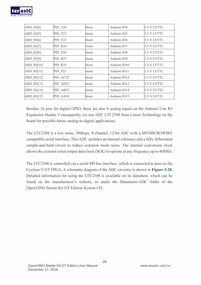
Besides 16 pins for digital GPIO, there are also 8 analog inputs on the Arduino Uno R3
Expansion Header. Consequently, we use ADC LTC2308 from Linear Technology on the
board for possible future analog-to-digital applications.
The LTC2308 is a low noise, 500ksps, 8-channel, 12-bit ADC with a SPI/MICROWIRE
compatible serial interface. This ADC includes an internal reference and a fully differential
sample-and-hold circuit to reduce common mode noise. The internal conversion clock
allows the external serial output data clock (SCK) to operate at any frequency up to 40MHz.
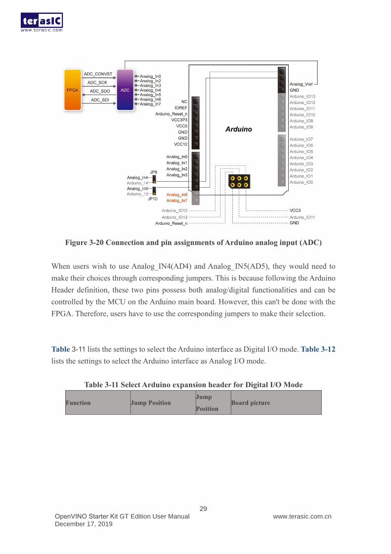
The LTC2308 is controlled via a serial SPI bus interface, which is connected to pins on the
Cyclone V GT FPGA. A schematic diagram of the ADC circuitry is shown in Figure 3-20.
Detailed information for using the LTC2308 is available on its datasheet, which can be
found on the manufacturer’s website, or under the Datasheets\ADC folder of the
OpenVINO Starter Kit GT Edition System CD.
OpenVINO Starter Kit GT Edition User Manual December 17, 2019
www.terasic.com.cn
29
Figure 3-20 Connection and pin assignments of Arduino analog input (ADC)
When users wish to use Analog_IN4(AD4) and Analog_IN5(AD5), they would need to
make their choices through corresponding jumpers. This is because following the Arduino
Header definition, these two pins possess both analog/digital functionalities and can be
controlled by the MCU on the Arduino main board. However, this can't be done with the
FPGA. Therefore, users have to use the corresponding jumpers to make their selection.
Table 3-11 lists the settings to select the Arduino interface as Digital I/O mode. Table 3-12
lists the settings to select the Arduino interface as Analog I/O mode.
Table 3-11 Select Arduino expansion header for Digital I/O Mode
Function Jump Position Jump
Position Board picture
OpenVINO Starter Kit GT Edition User Manual December 17, 2019
www.terasic.com.cn
30
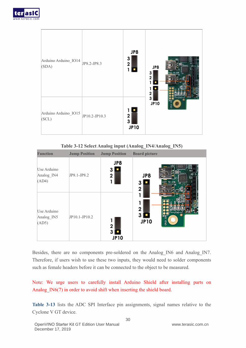
Arduino Arduino_IO14
(SDA) JP8.2-JP8.3
Arduino Arduino_IO15
(SCL) JP10.2-JP10.3
Table 3-12 Select Analog input (Analog_IN4/Analog_IN5)
Function Jump Position Jump Position Board picture
Use Arduino
Analog_IN4
(AD4)
JP8.1-JP8.2
Use Arduino
Analog_IN5
(AD5)
JP10.1-JP10.2
Besides, there are no components pre-soldered on the Analog_IN6 and Analog_IN7.
Therefore, if users wish to use these two inputs, they would need to solder components
such as female headers before it can be connected to the object to be measured.
Note: We urge users to carefully install Arduino Shield after installing parts on
Analog_IN6(7) in order to avoid shift when inserting the shield board.
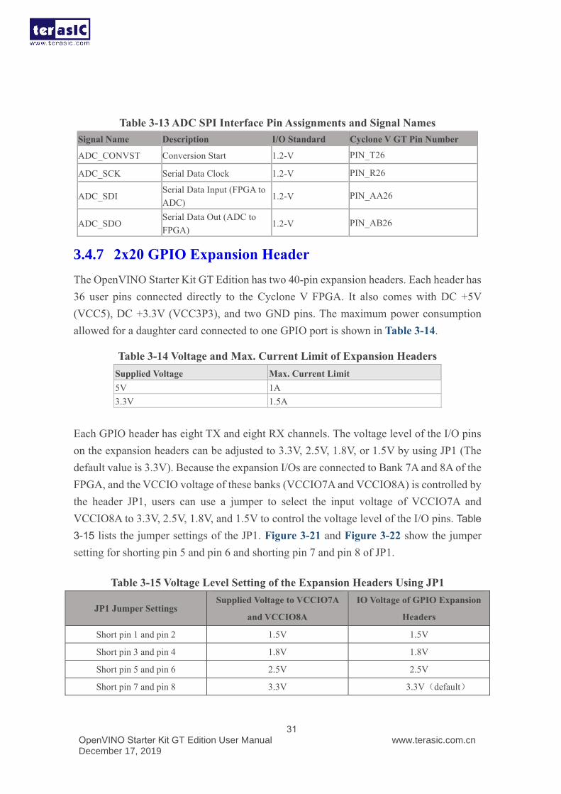
Table 3-13 lists the ADC SPI Interface pin assignments, signal names relative to the
Cyclone V GT device.
OpenVINO Starter Kit GT Edition User Manual December 17, 2019
www.terasic.com.cn
31
Table 3-13 ADC SPI Interface Pin Assignments and Signal Names
Signal Name Description I/O Standard Cyclone V GT Pin Number
ADC_CONVST Conversion Start 1.2-V PIN_T26
ADC_SCK Serial Data Clock 1.2-V PIN_R26
ADC_SDI Serial Data Input (FPGA to
ADC) 1.2-V PIN_AA26
ADC_SDO Serial Data Out (ADC to
FPGA) 1.2-V PIN_AB26
3.4.7 2x20 GPIO Expansion Header
The OpenVINO Starter Kit GT Edition has two 40-pin expansion headers. Each header has
36 user pins connected directly to the Cyclone V FPGA. It also comes with DC +5V
(VCC5), DC +3.3V (VCC3P3), and two GND pins. The maximum power consumption
allowed for a daughter card connected to one GPIO port is shown in Table 3-14.
Table 3-14 Voltage and Max. Current Limit of Expansion Headers
Supplied Voltage Max. Current Limit
5V 1A
3.3V 1.5A
Each GPIO header has eight TX and eight RX channels. The voltage level of the I/O pins
on the expansion headers can be adjusted to 3.3V, 2.5V, 1.8V, or 1.5V by using JP1 (The
default value is 3.3V). Because the expansion I/Os are connected to Bank 7A and 8A of the
FPGA, and the VCCIO voltage of these banks (VCCIO7A and VCCIO8A) is controlled by
the header JP1, users can use a jumper to select the input voltage of VCCIO7A and
VCCIO8A to 3.3V, 2.5V, 1.8V, and 1.5V to control the voltage level of the I/O pins. Table
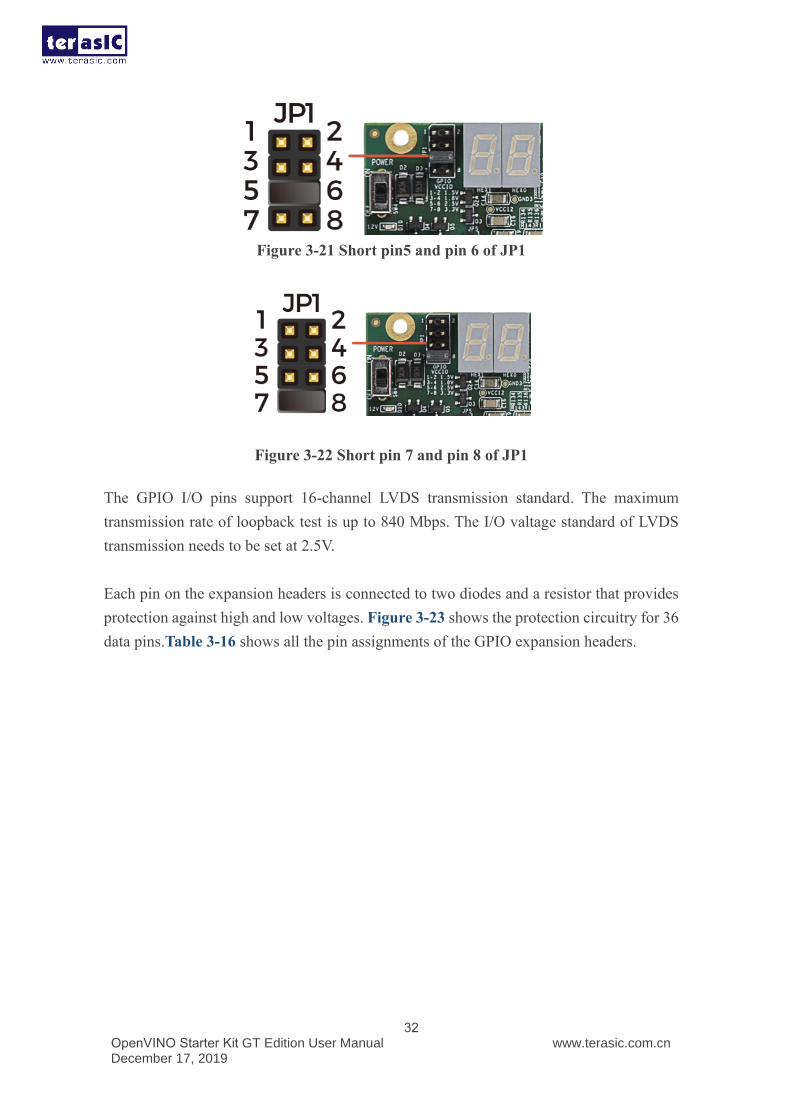
3-15 lists the jumper settings of the JP1. Figure 3-21 and Figure 3-22 show the jumper
setting for shorting pin 5 and pin 6 and shorting pin 7 and pin 8 of JP1.
Table 3-15 Voltage Level Setting of the Expansion Headers Using JP1
JP1 Jumper Settings Supplied Voltage to VCCIO7A
and VCCIO8A
IO Voltage of GPIO Expansion
Headers
Short pin 1 and pin 2 1.5V 1.5V
Short pin 3 and pin 4 1.8V 1.8V
Short pin 5 and pin 6 2.5V 2.5V
Short pin 7 and pin 8 3.3V 3.3V(default)
OpenVINO Starter Kit GT Edition User Manual December 17, 2019
www.terasic.com.cn
32
Figure 3-21 Short pin5 and pin 6 of JP1
Figure 3-22 Short pin 7 and pin 8 of JP1
The GPIO I/O pins support 16-channel LVDS transmission standard. The maximum
transmission rate of loopback test is up to 840 Mbps. The I/O valtage standard of LVDS
transmission needs to be set at 2.5V.
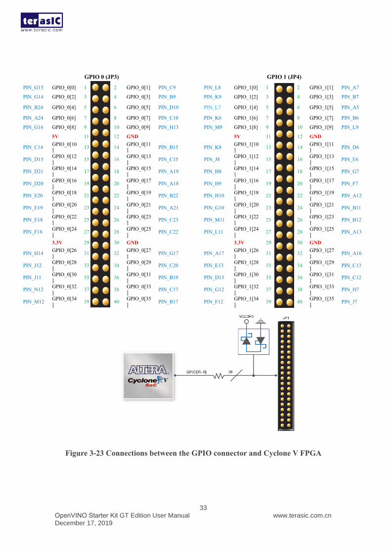
Each pin on the expansion headers is connected to two diodes and a resistor that provides
protection against high and low voltages. Figure 3-23 shows the protection circuitry for 36
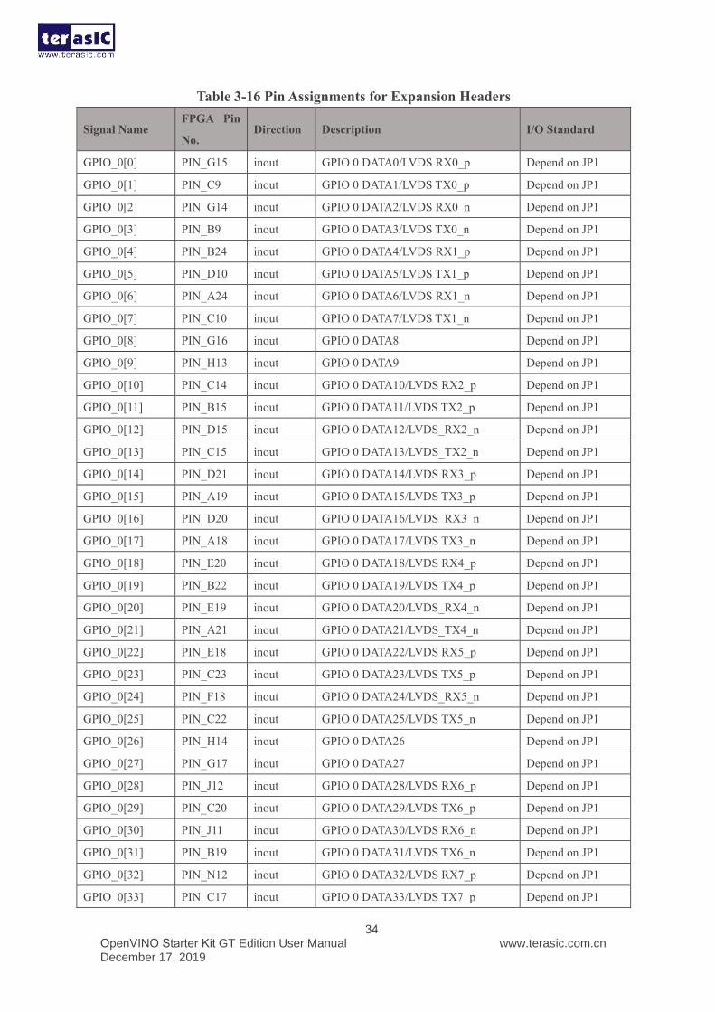
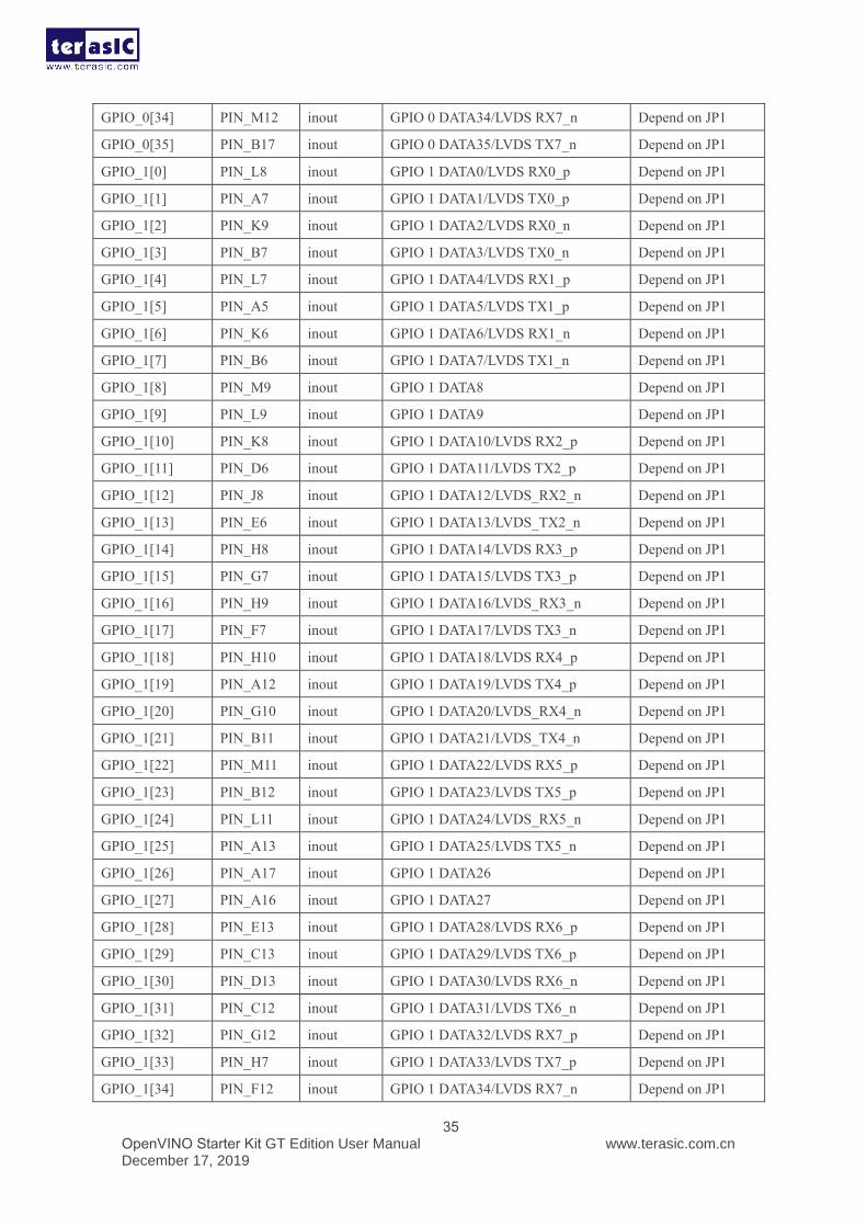
data pins.Table 3-16 shows all the pin assignments of the GPIO expansion headers.
OpenVINO Starter Kit GT Edition User Manual December 17, 2019
www.terasic.com.cn
33
Figure 3-23 Connections between the GPIO connector and Cyclone V FPGA
GPIO 0 (JP3) GPIO 1 (JP4)
PIN_G15 GPIO_0[0] 1 2 GPIO_0[1] PIN_C9 PIN_L8 GPIO_1[0] 1 2 GPIO_1[1] PIN_A7
PIN_G14 GPIO_0[2] 3 4 GPIO_0[3] PIN_B9 PIN_K9 GPIO_1[2] 3 4 GPIO_1[3] PIN_B7
PIN_B24 GPIO_0[4] 5 6 GPIO_0[5] PIN_D10 PIN_L7 GPIO_1[4] 5
6 GPIO_1[5] PIN_A5
PIN_A24 GPIO_0[6] 7 8 GPIO_0[7] PIN_C10 PIN_K6 GPIO_1[6] 7 8 GPIO_1[7] PIN_B6
PIN_G16 GPIO_0[8] 9 10 GPIO_0[9] PIN_H13 PIN_M9 GPIO_1[8] 9 10 GPIO_1[9] PIN_L9
5V 11 12 GND 5V 11 12 GND
PIN_C14 GPIO_0[10]
13 14 GPIO_0[11]
PIN_B15 PIN_K8 GPIO_1[10]
13 14 GPIO_1[11]
PIN_D6
PIN_D15 GPIO_0[12
] 15 16
GPIO_0[13
] PIN_C15 PIN_J8
GPIO_1[12
] 15 16
GPIO_1[13
] PIN_E6
PIN_D21 GPIO_0[14
] 17 18
GPIO_0[15
] PIN_A19 PIN_H8
GPIO_1[14
] 17 18
GPIO_1[15
] PIN_G7
PIN_D20 GPIO_0[16]
19 20 GPIO_0[17]
PIN_A18 PIN_H9 GPIO_1[16]
19 20 GPIO_1[17]
PIN_F7
PIN_E20 GPIO_0[18
] 21 22
GPIO_0[19
] PIN_B22 PIN_H10
GPIO_1[18
] 21 22
GPIO_1[19
] PIN_A12
PIN_E19 GPIO_0[20
] 23 24
GPIO_0[21
] PIN_A21 PIN_G10
GPIO_1[20
] 23 24
GPIO_1[21
] PIN_B11
PIN_E18 GPIO_0[22
] 25 26
GPIO_0[23
] PIN_C23 PIN_M11
GPIO_1[22
] 25 26
GPIO_1[23
] PIN_B12
PIN_F18 GPIO_0[24]
27 28 GPIO_0[25]
PIN_C22 PIN_L11 GPIO_1[24]
27 28 GPIO_1[25]
PIN_A13
3.3V 29 30 GND 3.3V 29 30 GND
PIN_H14 GPIO_0[26
] 31 32
GPIO_0[27
] PIN_G17 PIN_A17
GPIO_1[26
] 31 32
GPIO_1[27
] PIN_A16
PIN_J12 GPIO_0[28
] 33 34
GPIO_0[29
] PIN_C20 PIN_E13
GPIO_1[28
] 33 34
GPIO_1[29
] PIN_C13
PIN_J11 GPIO_0[30]
35 36 GPIO_0[31]
PIN_B19 PIN_D13 GPIO_1[30]
35 36 GPIO_1[31]
PIN_C12
PIN_N12 GPIO_0[32
] 37 38
GPIO_0[33
] PIN_C17 PIN_G12
GPIO_1[32
] 37 38
GPIO_1[33
] PIN_H7
PIN_M12 GPIO_0[34
] 39 40
GPIO_0[35
] PIN_B17 PIN_F12
GPIO_1[34
] 39 40
GPIO_1[35
] PIN_J7
OpenVINO Starter Kit GT Edition User Manual December 17, 2019
www.terasic.com.cn
34
Table 3-16 Pin Assignments for Expansion Headers
Signal Name FPGA Pin
No. Direction Description I/O Standard
GPIO_0[0] PIN_G15 inout GPIO 0 DATA0/LVDS RX0_p Depend on JP1
GPIO_0[1] PIN_C9 inout GPIO 0 DATA1/LVDS TX0_p Depend on JP1
GPIO_0[2] PIN_G14 inout GPIO 0 DATA2/LVDS RX0_n Depend on JP1
GPIO_0[3] PIN_B9 inout GPIO 0 DATA3/LVDS TX0_n Depend on JP1
GPIO_0[4] PIN_B24 inout GPIO 0 DATA4/LVDS RX1_p Depend on JP1
GPIO_0[5] PIN_D10 inout GPIO 0 DATA5/LVDS TX1_p Depend on JP1
GPIO_0[6] PIN_A24 inout GPIO 0 DATA6/LVDS RX1_n Depend on JP1
GPIO_0[7] PIN_C10 inout GPIO 0 DATA7/LVDS TX1_n Depend on JP1
GPIO_0[8] PIN_G16 inout GPIO 0 DATA8 Depend on JP1
GPIO_0[9] PIN_H13 inout GPIO 0 DATA9 Depend on JP1
GPIO_0[10] PIN_C14 inout GPIO 0 DATA10/LVDS RX2_p Depend on JP1
GPIO_0[11] PIN_B15 inout GPIO 0 DATA11/LVDS TX2_p Depend on JP1
GPIO_0[12] PIN_D15 inout GPIO 0 DATA12/LVDS_RX2_n Depend on JP1
GPIO_0[13] PIN_C15 inout GPIO 0 DATA13/LVDS_TX2_n Depend on JP1
GPIO_0[14] PIN_D21 inout GPIO 0 DATA14/LVDS RX3_p Depend on JP1
GPIO_0[15] PIN_A19 inout GPIO 0 DATA15/LVDS TX3_p Depend on JP1
GPIO_0[16] PIN_D20 inout GPIO 0 DATA16/LVDS_RX3_n Depend on JP1
GPIO_0[17] PIN_A18 inout GPIO 0 DATA17/LVDS TX3_n Depend on JP1
GPIO_0[18] PIN_E20 inout GPIO 0 DATA18/LVDS RX4_p Depend on JP1
GPIO_0[19] PIN_B22 inout GPIO 0 DATA19/LVDS TX4_p Depend on JP1
GPIO_0[20] PIN_E19 inout GPIO 0 DATA20/LVDS_RX4_n Depend on JP1
GPIO_0[21] PIN_A21 inout GPIO 0 DATA21/LVDS_TX4_n Depend on JP1
GPIO_0[22] PIN_E18 inout GPIO 0 DATA22/LVDS RX5_p Depend on JP1
GPIO_0[23] PIN_C23 inout GPIO 0 DATA23/LVDS TX5_p Depend on JP1
GPIO_0[24] PIN_F18 inout GPIO 0 DATA24/LVDS_RX5_n Depend on JP1
GPIO_0[25] PIN_C22 inout GPIO 0 DATA25/LVDS TX5_n Depend on JP1
GPIO_0[26] PIN_H14 inout GPIO 0 DATA26 Depend on JP1
GPIO_0[27] PIN_G17 inout GPIO 0 DATA27 Depend on JP1
GPIO_0[28] PIN_J12 inout GPIO 0 DATA28/LVDS RX6_p Depend on JP1
GPIO_0[29] PIN_C20 inout GPIO 0 DATA29/LVDS TX6_p Depend on JP1
GPIO_0[30] PIN_J11 inout GPIO 0 DATA30/LVDS RX6_n Depend on JP1
GPIO_0[31] PIN_B19 inout GPIO 0 DATA31/LVDS TX6_n Depend on JP1
GPIO_0[32] PIN_N12 inout GPIO 0 DATA32/LVDS RX7_p Depend on JP1
GPIO_0[33] PIN_C17 inout GPIO 0 DATA33/LVDS TX7_p Depend on JP1
OpenVINO Starter Kit GT Edition User Manual December 17, 2019
www.terasic.com.cn
35
GPIO_0[34] PIN_M12 inout GPIO 0 DATA34/LVDS RX7_n Depend on JP1
GPIO_0[35] PIN_B17 inout GPIO 0 DATA35/LVDS TX7_n Depend on JP1
GPIO_1[0] PIN_L8 inout GPIO 1 DATA0/LVDS RX0_p Depend on JP1
GPIO_1[1] PIN_A7 inout GPIO 1 DATA1/LVDS TX0_p Depend on JP1
GPIO_1[2] PIN_K9 inout GPIO 1 DATA2/LVDS RX0_n Depend on JP1
GPIO_1[3] PIN_B7 inout GPIO 1 DATA3/LVDS TX0_n Depend on JP1
GPIO_1[4] PIN_L7 inout GPIO 1 DATA4/LVDS RX1_p Depend on JP1
GPIO_1[5] PIN_A5 inout GPIO 1 DATA5/LVDS TX1_p Depend on JP1
GPIO_1[6] PIN_K6 inout GPIO 1 DATA6/LVDS RX1_n Depend on JP1
GPIO_1[7] PIN_B6 inout GPIO 1 DATA7/LVDS TX1_n Depend on JP1
GPIO_1[8] PIN_M9 inout GPIO 1 DATA8 Depend on JP1
GPIO_1[9] PIN_L9 inout GPIO 1 DATA9 Depend on JP1
GPIO_1[10] PIN_K8 inout GPIO 1 DATA10/LVDS RX2_p Depend on JP1
GPIO_1[11] PIN_D6 inout GPIO 1 DATA11/LVDS TX2_p Depend on JP1
GPIO_1[12] PIN_J8 inout GPIO 1 DATA12/LVDS_RX2_n Depend on JP1
GPIO_1[13] PIN_E6 inout GPIO 1 DATA13/LVDS_TX2_n Depend on JP1
GPIO_1[14] PIN_H8 inout GPIO 1 DATA14/LVDS RX3_p Depend on JP1
GPIO_1[15] PIN_G7 inout GPIO 1 DATA15/LVDS TX3_p Depend on JP1
GPIO_1[16] PIN_H9 inout GPIO 1 DATA16/LVDS_RX3_n Depend on JP1
GPIO_1[17] PIN_F7 inout GPIO 1 DATA17/LVDS TX3_n Depend on JP1
GPIO_1[18] PIN_H10 inout GPIO 1 DATA18/LVDS RX4_p Depend on JP1
GPIO_1[19] PIN_A12 inout GPIO 1 DATA19/LVDS TX4_p Depend on JP1
GPIO_1[20] PIN_G10 inout GPIO 1 DATA20/LVDS_RX4_n Depend on JP1
GPIO_1[21] PIN_B11 inout GPIO 1 DATA21/LVDS_TX4_n Depend on JP1
GPIO_1[22] PIN_M11 inout GPIO 1 DATA22/LVDS RX5_p Depend on JP1
GPIO_1[23] PIN_B12 inout GPIO 1 DATA23/LVDS TX5_p Depend on JP1
GPIO_1[24] PIN_L11 inout GPIO 1 DATA24/LVDS_RX5_n Depend on JP1
GPIO_1[25] PIN_A13 inout GPIO 1 DATA25/LVDS TX5_n Depend on JP1
GPIO_1[26] PIN_A17 inout GPIO 1 DATA26 Depend on JP1
GPIO_1[27] PIN_A16 inout GPIO 1 DATA27 Depend on JP1
GPIO_1[28] PIN_E13 inout GPIO 1 DATA28/LVDS RX6_p Depend on JP1
GPIO_1[29] PIN_C13 inout GPIO 1 DATA29/LVDS TX6_p Depend on JP1
GPIO_1[30] PIN_D13 inout GPIO 1 DATA30/LVDS RX6_n Depend on JP1
GPIO_1[31] PIN_C12 inout GPIO 1 DATA31/LVDS TX6_n Depend on JP1
GPIO_1[32] PIN_G12 inout GPIO 1 DATA32/LVDS RX7_p Depend on JP1
GPIO_1[33] PIN_H7 inout GPIO 1 DATA33/LVDS TX7_p Depend on JP1
GPIO_1[34] PIN_F12 inout GPIO 1 DATA34/LVDS RX7_n Depend on JP1

OpenVINO Starter Kit GT Edition User Manual December 17, 2019
www.terasic.com.cn
36
GPIO_1[35] PIN_J7 inout GPIO 1 DATA35/LVDS TX7_n Depend on JP1
OpenVINO Starter Kit GT Edition User Manual December 17, 2019
www.terasic.com.cn
37
Chapter 4
OpenVINO Starter Kit GT Edition
System Builder
This chapter describes how users can create a custom design project on the board by using
the OpenVINO Starter Kit GT Edition System Builder.Besides, users can also use the
Quartus Golden top for the project building. Golden top project is located in folder:
CD\Demonstration.
4.1 Introduction
The OpenVINO Starter Kit GT Edition System Builder is a Windows-based software utility,
designed to assist users to create a Quartus Prime project for the board within minutes. The
generated Quartus Prime project files include:
⚫ Quartus Prime project file (.qpf)
⚫ Quartus Prime setting file (.qsf)
⚫ Top-level design file (.v or .vhd)
⚫ Synopsis design constraints file (.sdc)
⚫ Pin assignment document (.htm)
By providing the above files, the OpenVINO Starter Kit GT Edition System Builder
prevents occurrence of situations that are prone to errors when users manually edit the top-
level design file or place pin assignments. The common mistakes that users encounter are
shown below:
⚫ OpenVINO Starter Kit GT Edition board damage due to wrong pin/bank voltage
assignments.
⚫ OpenVINO Starter Kit GT Edition board malfunction caused by wrong device
connections or missing pin counts for connected ends.
⚫ Performance degradation due to improper pin assignments.
4.2 General Design Flow
This section will introduce the general design flow to build a project for the development
board via the OpenVINO Starter Kit GT Edition System Builder. The general design flow
is illustrated in Figure 4-1.
Users should launch the OpenVINO Starter Kit GT Edition System Builder and create a
new project according to their design requirements. When users complete the settings, the
OpenVINO Starter Kit GT Edition User Manual December 17, 2019
www.terasic.com.cn
38
OpenVINO Starter Kit GT Edition System Builder will generate two major files, a top-
level design file (.v or .vhd) and a Quartus Prime setting file (.qsf).
The top-level design file contains top-level Verilog or VHDL HDL wrapper for users to
add their own design/logic. The Quartus Prime setting file contains information such as
FPGA device type, top-level pin assignments, and the I/O standard for each user-defined
I/O pin.
Finally, the Quartus Prime programmer must be used to download .sof file to the
OpenVINO Starter Kit GT Edition development board using a JTAG interface.
Figure 4-1 The general design flow of building a design
4.3 Using OpenVINO Starter Kit GT Edition System
Builder
This section provides detailed procedures on how to use the OpenVINO Starter Kit GT
Edition System Builder.
◼ Install and launch OpenVINO Starter Kit GT Edition System Builder
The OpenVINO Starter Kit GT Edition System Builder is located in the directory:
“Tools\SystemBuilder” in the OpenVINO Starter Kit GT Edition System CD. Users can
copy the whole folder to a host computer without installing the utility. Launch the
OpenVINO Starter Kit GT Edition User Manual December 17, 2019
www.terasic.com.cn
39
OpenVINO Starter Kit GT Edition System Builder by executing the OpenVINO Starter Kit
GT Edition _SystemBuilder.exe on the host computer and the GUI window will appear as
shown in Figure 4-2.
Figure 4-2 OpenVINO Starter Kit GT EditionSystem Builder window
◼ Input Project Name
Input project name as shown in Figure 4-3, type in an appropriate name in the green circled
area, it will automatically be assigned as the name of your top-level design entity.
OpenVINO Starter Kit GT Edition User Manual December 17, 2019
www.terasic.com.cn
40
Figure 4-3 Board Type and Project Name
◼ System Configuration
Under the System Configuration users are given the flexibility of enabling their choice of
components included on the board as shown in Figure 4-4, each component of the board
is listed where users can enable or disable a component according to their design by simply
marking a check or removing the check in the field provided. If the component is enabled,
the OpenVINO Starter Kit GT Edition System Builder will automatically generate the
associated pin assignments including the pin name, pin location, pin direction, and I/O
standard.

OpenVINO Starter Kit GT Edition User Manual December 17, 2019
www.terasic.com.cn
41
Figure 4-4 System Configuration Group
◼ GPIO Expansion
Users can connect Terasic GPIO daughter cards onto the GPIO connector located on the
development board. As shown in Figure 4-5, the OpenVINO Starter Kit GT Edition System
Builder will generate a project that includes related module. It will automatically generate
the associated pin assignment including pin name, pin location, pin direction, and I/O
standard.
OpenVINO Starter Kit GT Edition User Manual December 17, 2019
www.terasic.com.cn
42
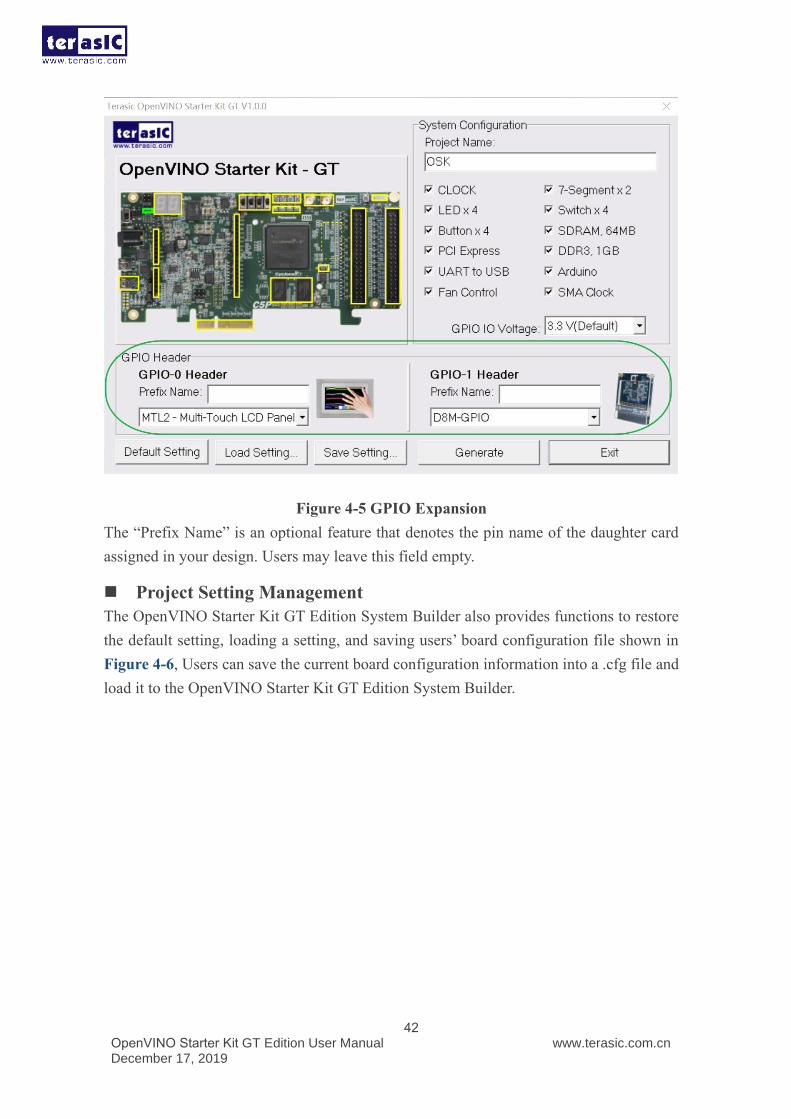
Figure 4-5 GPIO Expansion
The “Prefix Name” is an optional feature that denotes the pin name of the daughter card
assigned in your design. Users may leave this field empty.
◼ Project Setting Management
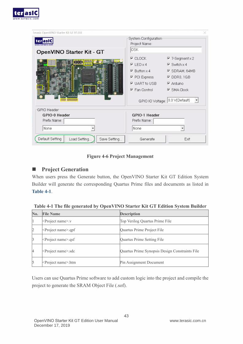
The OpenVINO Starter Kit GT Edition System Builder also provides functions to restore
the default setting, loading a setting, and saving users’ board configuration file shown in
Figure 4-6, Users can save the current board configuration information into a .cfg file and
load it to the OpenVINO Starter Kit GT Edition System Builder.
OpenVINO Starter Kit GT Edition User Manual December 17, 2019
www.terasic.com.cn
43
Figure 4-6 Project Management
◼ Project Generation
When users press the Generate button, the OpenVINO Starter Kit GT Edition System
Builder will generate the corresponding Quartus Prime files and documents as listed in
Table 4-1.
Table 4-1 The file generated by OpenVINO Starter Kit GT Edition System Builder
No. File Name Description
1 <Project name>.v Top Verilog Quartus Prime File
2 <Project name>.qpf Quartus Prime Project File
3 <Project name>.qsf Quartus Prime Setting File
4 <Project name>.sdc Quartus Prime Synopsis Design Constraints File
5 <Project name>.htm Pin Assignment Document
Users can use Quartus Prime software to add custom logic into the project and compile the
project to generate the SRAM Object File (.sof).
OpenVINO Starter Kit GT Edition User Manual December 17, 2019
www.terasic.com.cn
44
Chapter 5
Examples of Advanced
Demonstrations This chapter introduces several advanced demos designed by using RTL or Qsys. These
examples provide demonstrations of the major features which are connected to the FPGA
interface on the board, such as audio, SDRAM and IR Receiver. All these associated files
can be found in the Demonstrations folder on the OpenVINO Starter Kit GT Edition
System CD.
◼ Demonstration Installation
How to run the Demonstaions with the computer:
Copy the Demonstration folder to the selected local directory, make sure that the path to
the local directory does not contain the whitespace, otherwise the Nios II will run with error.
Note that you must install the v17.1 or later Quartus Prime (including Cyclone V device)
to run the OpenVINO Starter Kit GT Edition design example.
5.1 OpenVINO Starter Kit GT Edition Factory Default
Configuration
The OpenVINO Starter Kit GT Edition is shipped from the factory with a default
configuration bit-stream that demonstrates some of the basic features of the board, such as
scrolling LED Marquee, HEX goes from 0 to F. The setup required for this demonstration,
and the locations of its files are explained below.
◼ Demonstration Setup and Instructions
⚫ Project directory: Default.
⚫ Demo Batch File: Default\demo_batch_jic\test.bat.
⚫ FPGA Configure File: Default.sof or Default.jic.
⚫ Connect the USB cable provided to the USB Blaster II port on the OpenVINO
Starter Kit GT Edition. Ensure that power is applied to the OpenVINO Starter
Kit GT Edition. If necessary(EPCQ is erased), please program the default code
into EPCQ via the JTAG connection for the factory default configuration.
⚫ Now, the 7-segment displays are enabled to display from 0 to F, and the LED is
flashing.
⚫ The project also provides the demo_batch folder for running easily. By running
OpenVINO Starter Kit GT Edition User Manual December 17, 2019
www.terasic.com.cn
45
the test.bat,it is not only able to download the .sof into FPGA by command, but
also to enable it to convert .sof to .jic file, which can be used to program the
EPCQ device.
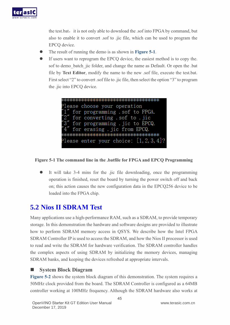
⚫ The result of running the demo is as shown in Figure 5-1.
⚫ If users want to reprogram the EPCQ device, the easiest method is to copy the.
sof to demo_batch_jic folder, and change the name as Default. Or open the .bat
file by Text Editor, modify the name to the new .sof file, execute the test.bat.
First select “2” to convert .sof file to .jic file, then select the option “3” to program
the .jic into EPCQ device.
Figure 5-1 The command line in the .batfile for FPGA and EPCQ Programming
⚫ It will take 3-4 mins for the .jic file downloading, once the programming
operation is finished, reset the board by turning the power switch off and back
on; this action causes the new configuration data in the EPCQ256 device to be
loaded into the FPGA chip.
5.2 Nios II SDRAM Test
Many applications use a high-performance RAM, such as a SDRAM, to provide temporary
storage. In this demonstration the hardware and software designs are provided to illustrate
how to perform SDRAM memory access in QSYS. We describe how the Intel FPGA
SDRAM Controller IP is used to access the SDRAM, and how the Nios II processor is used
to read and write the SDRAM for hardware verification. The SDRAM controller handles
the complex aspects of using SDRAM by initializing the memory devices, managing
SDRAM banks, and keeping the devices refreshed at appropriate intervals.
◼ System Block Diagram
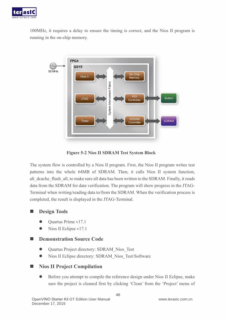
Figure 5-2 shows the system block diagram of this demonstration. The system requires a
50MHz clock provided from the board. The SDRAM Controller is configured as a 64MB
controller working at 100MHz frequency. Although the SDRAM hardware also works at
OpenVINO Starter Kit GT Edition User Manual December 17, 2019
www.terasic.com.cn
46
100MHz, it requires a delay to ensure the timing is correct, and the Nios II program is
running in the on-chip memory.
Figure 5-2 Nios II SDRAM Test System Block
The system flow is controlled by a Nios II program. First, the Nios II program writes test
patterns into the whole 64MB of SDRAM. Then, it calls Nios II system function,
alt_dcache_flush_all, to make sure all data has been written to the SDRAM. Finally, it reads
data from the SDRAM for data verification. The program will show progress in the JTAG-
Terminal when writing/reading data to/from the SDRAM. When the verification process is
completed, the result is displayed in the JTAG-Terminal.
◼ Design Tools
⚫ Quartus Prime v17.1
⚫ Nios II Eclipse v17.1
◼ Demonstration Source Code
⚫ Quartus Project directory: SDRAM_Nios_Test
⚫ Nios II Eclipse directory: SDRAM_Nios_Test\Software
◼ Nios II Project Compilation
⚫ Before you attempt to compile the reference design under Nios II Eclipse, make
sure the project is cleaned first by clicking ‘Clean’ from the ‘Project’ menu of
OpenVINO Starter Kit GT Edition User Manual December 17, 2019
www.terasic.com.cn
47
Nios II Eclipse. Refer to the OpenVINO Starter Kit_My_First_NiosII document
for more details.
◼ Demonstration Batch File
Demo Batch File Folder: SDRAM_Nios_Test \demo_batch.
The demo batch file includes following files:
⚫ USB-Blaster II Batch File: test.bat、test.sh
⚫ FPGA Configuration File: SDRAM_Nios_Test.sof
⚫ Nios II Program: SDRAM_Nios_Test.elf
◼ Demonstration Setup
⚫ Make sure the Quartus Prime v17.1, Nios II v17.1 and USB-Blaster II driver are
installed on your PC.
⚫ Use USB cable to connect PC and the OpenVINO Starter Kit GT Edition(J5),
power on the board.
⚫ Execute the demo batch file “test.bat” under the batch file folder:
SDRAM_Nios_Test\demo_batch for project running.
⚫ After Nios II program is downloaded and executed successfully, a prompt
message will be displayed in nios2-terminal.
⚫ Press KEY0 or KEY1 of the OpenVINO Starter Kit GT Edition to start the
SDRAM verify process. Press KEY0 for test continued.
⚫ The program will display progressing and result information, as shown in Figure
5-3.
OpenVINO Starter Kit GT Edition User Manual December 17, 2019
www.terasic.com.cn
48
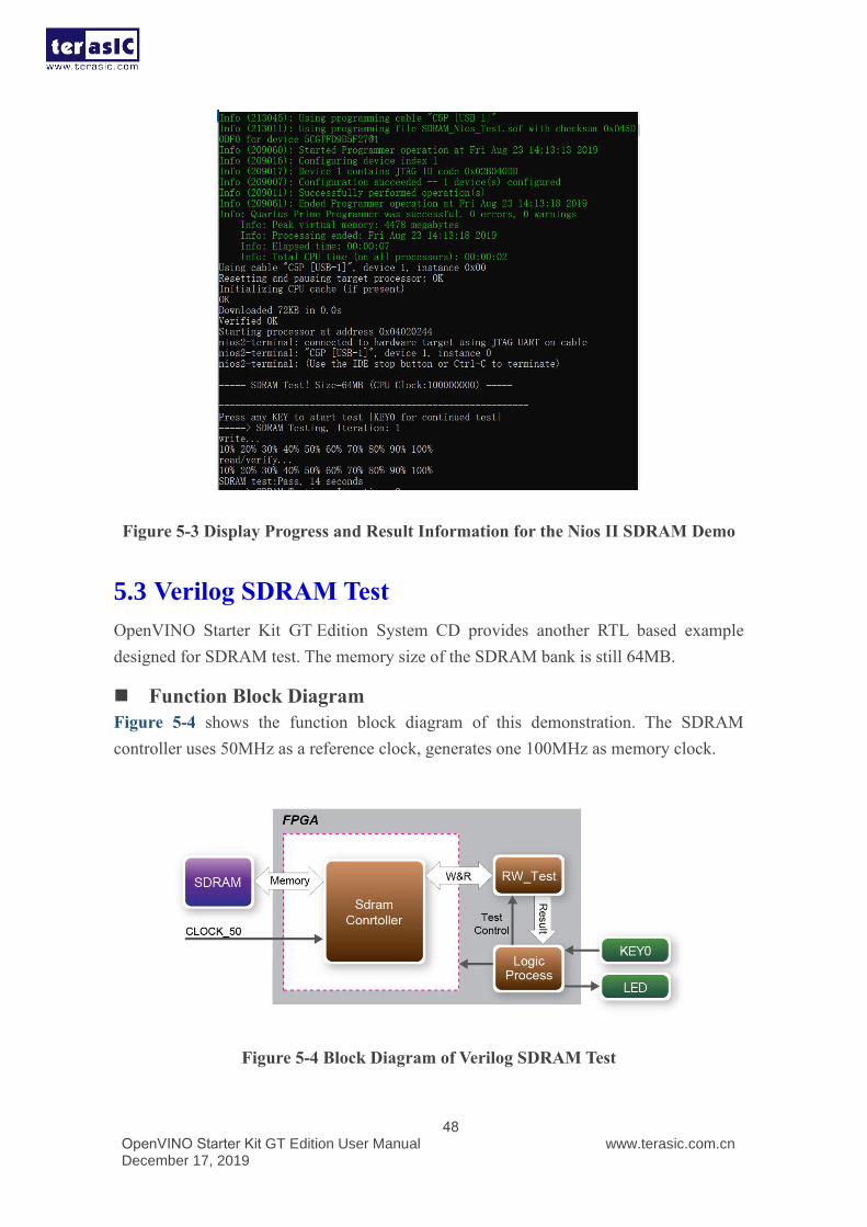
Figure 5-3 Display Progress and Result Information for the Nios II SDRAM Demo
5.3 Verilog SDRAM Test
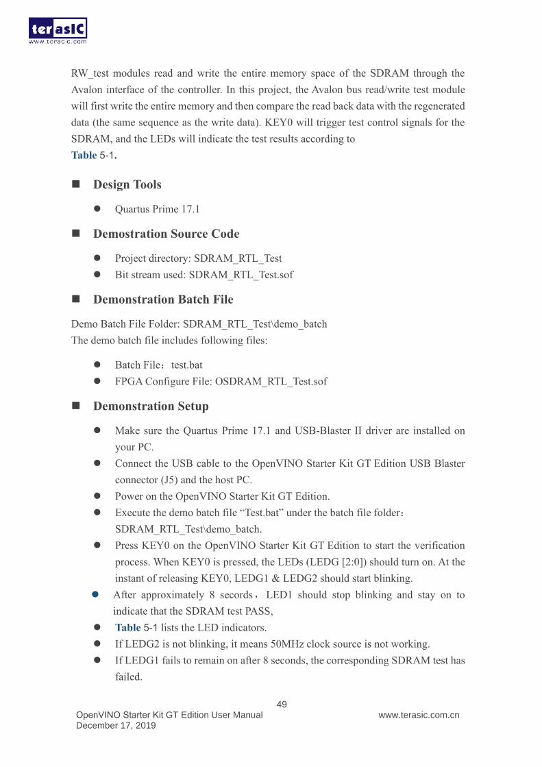
OpenVINO Starter Kit GT Edition System CD provides another RTL based example
designed for SDRAM test. The memory size of the SDRAM bank is still 64MB.
◼ Function Block Diagram
Figure 5-4 shows the function block diagram of this demonstration. The SDRAM
controller uses 50MHz as a reference clock, generates one 100MHz as memory clock.
Figure 5-4 Block Diagram of Verilog SDRAM Test
OpenVINO Starter Kit GT Edition User Manual December 17, 2019
www.terasic.com.cn
49
RW_test modules read and write the entire memory space of the SDRAM through the
Avalon interface of the controller. In this project, the Avalon bus read/write test module
will first write the entire memory and then compare the read back data with the regenerated
data (the same sequence as the write data). KEY0 will trigger test control signals for the
SDRAM, and the LEDs will indicate the test results according to
Table 5-1.
◼ Design Tools
⚫ Quartus Prime 17.1
◼ Demostration Source Code
⚫ Project directory: SDRAM_RTL_Test
⚫ Bit stream used: SDRAM_RTL_Test.sof
◼ Demonstration Batch File
Demo Batch File Folder: SDRAM_RTL_Test\demo_batch
The demo batch file includes following files:
⚫ Batch File:test.bat
⚫ FPGA Configure File: OSDRAM_RTL_Test.sof
◼ Demonstration Setup
⚫ Make sure the Quartus Prime 17.1 and USB-Blaster II driver are installed on
your PC.
⚫ Connect the USB cable to the OpenVINO Starter Kit GT Edition USB Blaster
connector (J5) and the host PC.
⚫ Power on the OpenVINO Starter Kit GT Edition.
⚫ Execute the demo batch file “Test.bat” under the batch file folder:
SDRAM_RTL_Test\demo_batch.
⚫ Press KEY0 on the OpenVINO Starter Kit GT Edition to start the verification
process. When KEY0 is pressed, the LEDs (LEDG [2:0]) should turn on. At the
instant of releasing KEY0, LEDG1 & LEDG2 should start blinking.
⚫ After approximately 8 secords,LED1 should stop blinking and stay on to
indicate that the SDRAM test PASS,
⚫ Table 5-1 lists the LED indicators.
⚫ If LEDG2 is not blinking, it means 50MHz clock source is not working.
⚫ If LEDG1 fails to remain on after 8 seconds, the corresponding SDRAM test has
failed.
OpenVINO Starter Kit GT Edition User Manual December 17, 2019
www.terasic.com.cn
50
⚫ Press KEY0 again to regenerate the test control signals for a new test.
Table 5-1 LED Indicators
Name Description
LEDG0 Reset
LEDG1 If light after KEY0 releasing, SDRAM test pass
LEDG2 It blinks indicating 50MHz clock source work
well
5.4 DDR3 SDRAM Test
This demonstration presents a memory test function on the bank of DDR3 SDRAM on the
OpenVINO Starter Kit GT Edition. The memory size of the DDR3 SDRAM bank is 1GB.
Cyclone V device supports both hard memory controller and software memory controller.
In this demo, the hard memory controller is used.
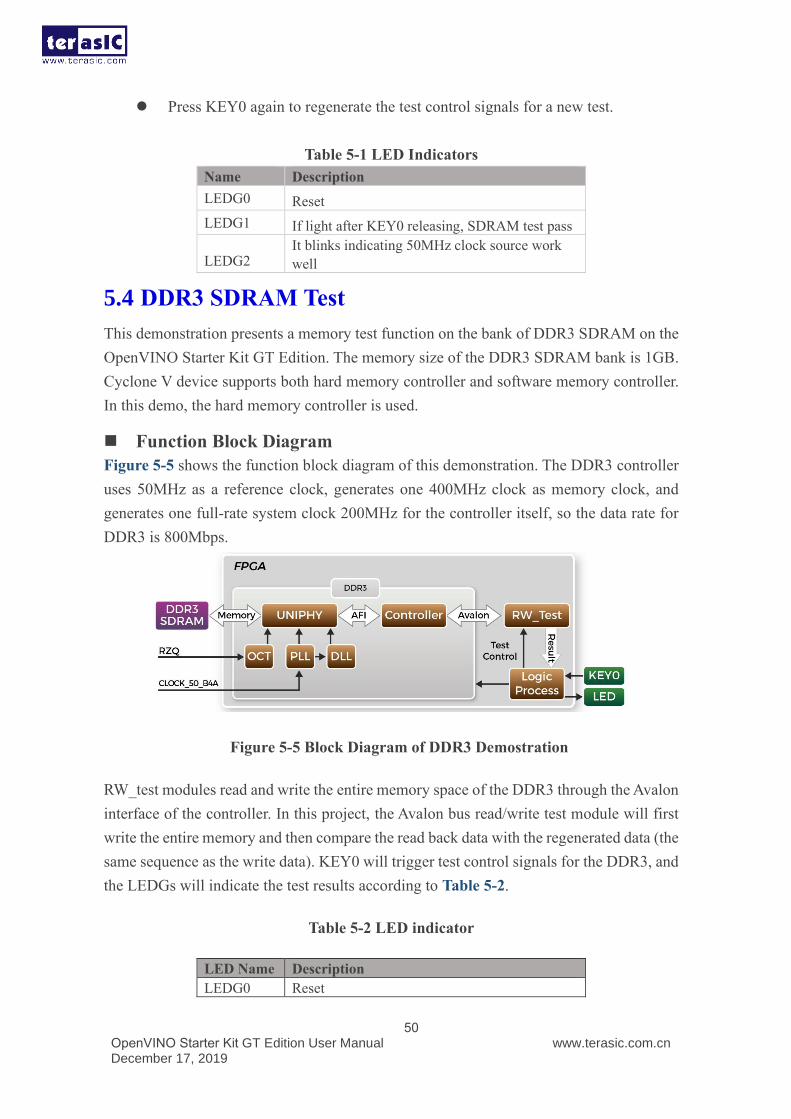
◼ Function Block Diagram
Figure 5-5 shows the function block diagram of this demonstration. The DDR3 controller
uses 50MHz as a reference clock, generates one 400MHz clock as memory clock, and
generates one full-rate system clock 200MHz for the controller itself, so the data rate for
DDR3 is 800Mbps.
Figure 5-5 Block Diagram of DDR3 Demostration
RW_test modules read and write the entire memory space of the DDR3 through the Avalon
interface of the controller. In this project, the Avalon bus read/write test module will first
write the entire memory and then compare the read back data with the regenerated data (the
same sequence as the write data). KEY0 will trigger test control signals for the DDR3, and
the LEDGs will indicate the test results according to Table 5-2.
Table 5-2 LED indicator
LED Name Description
LEDG0 Reset
OpenVINO Starter Kit GT Edition User Manual December 17, 2019
www.terasic.com.cn
51
LEDG1 If light, DDR3 test pass
LEDG2
It blinks indicating 50MHz clock source work
well
◼ DDR3 SDRAM Controller with UniPHY
To use DDR3 controller, users need to perform the three major steps:
⚫ Create correct pin assignments for the DDR3.
⚫ Perform “Analysis and Synthesis” by selecting from the Quartus Prime menu
Processing→Start→Start Analysis & Synthesis.
⚫ Run the TCL files generated by DDR3 IP by selecting from the Quartus Prime
menu Tools→TCL Scripts.
◼ Design Tools
⚫ Quartus Prime v17.1
◼ Demonstration Source Code
⚫ Project directory: DDR3_RTL_Test
⚫ Bitstream File: DDR3_RTL_Test.sof
◼ Demonstration Batch File
Demo Batch File Folder:DDR3_RTL_Test \demo_batch
The demo batch file includes following files:
⚫ Batch File: test.bat
⚫ FPGA Configure File: DDR3_RTL_Test.sof
◼ Demonstration Setup
⚫ Make sure the Quartus Prime v17.1 & USB-Blaster II driver are installed on your
PC.
⚫ Connect the USB cable to the USB Blaster II connector (J5) on the OpenVINO
Starter Kit GT Edition and host PC.
⚫ Power on the OpenVINO Starter Kit GT Edition.
⚫ Execute the demo batch file “test.bat” under the batch file folder:
DDR3_RTL_Test\demo_batch.
⚫ Press KEY0 on the OpenVINO Starter Kit GT Edition to start the verification
process. When KEY0 is pressed, the LEDs (LEDG [2:0]) should turn on. At the
instant of releasing KEY0, LEDG1, LEDG2 should start blinking. After
OpenVINO Starter Kit GT Edition User Manual December 17, 2019
www.terasic.com.cn
52
approximately 1 seconds, LEDG1 should stop blinking and stay on to indicate
that the DDR3 has passed the test, respectively, Table 5-2 lists the LED
indicators.
⚫ If LEDG2 is not blinking, it means 50MHz clock source is not working.
⚫ If LEDG1 does not light up after releasing KEY0, it indicates the DDR3
initializing failed.
⚫ If LEDG1 still keeps flashing after 1 second, the corresponding DDR3 test has
failed.
⚫ Press KEY0 again to regenerate the test control signals for a new test.
5.5 DDR3 SDRAM Test by Nios II
Many applications use a high-performance RAM, such as a DDR3 SDRAM Controller
with UniPHY IP, to provide temporary storage. In this demonstration hardware and
software designs are provided to illustrate how to perform DDR3 memory access in QSYS.
We describe how the Altera’s “DDR3 SDRAM Controller with UniPHY IP” is used to
access the DDR3-SDRAM, and how the Nios II processor is used to read and write the
SDRAM for hardware verification. The DDR3 SDRAM controller handles the complex
aspects of using DDR3 SDRAM by initializing the memory devices, managing SDRAM
banks, and keeping the devices refreshed at appropriate intervals. Cyclone V series deivce
supports both hard memory IP and soft memory IP. In this demonstration, it uses the hard
memory IP.
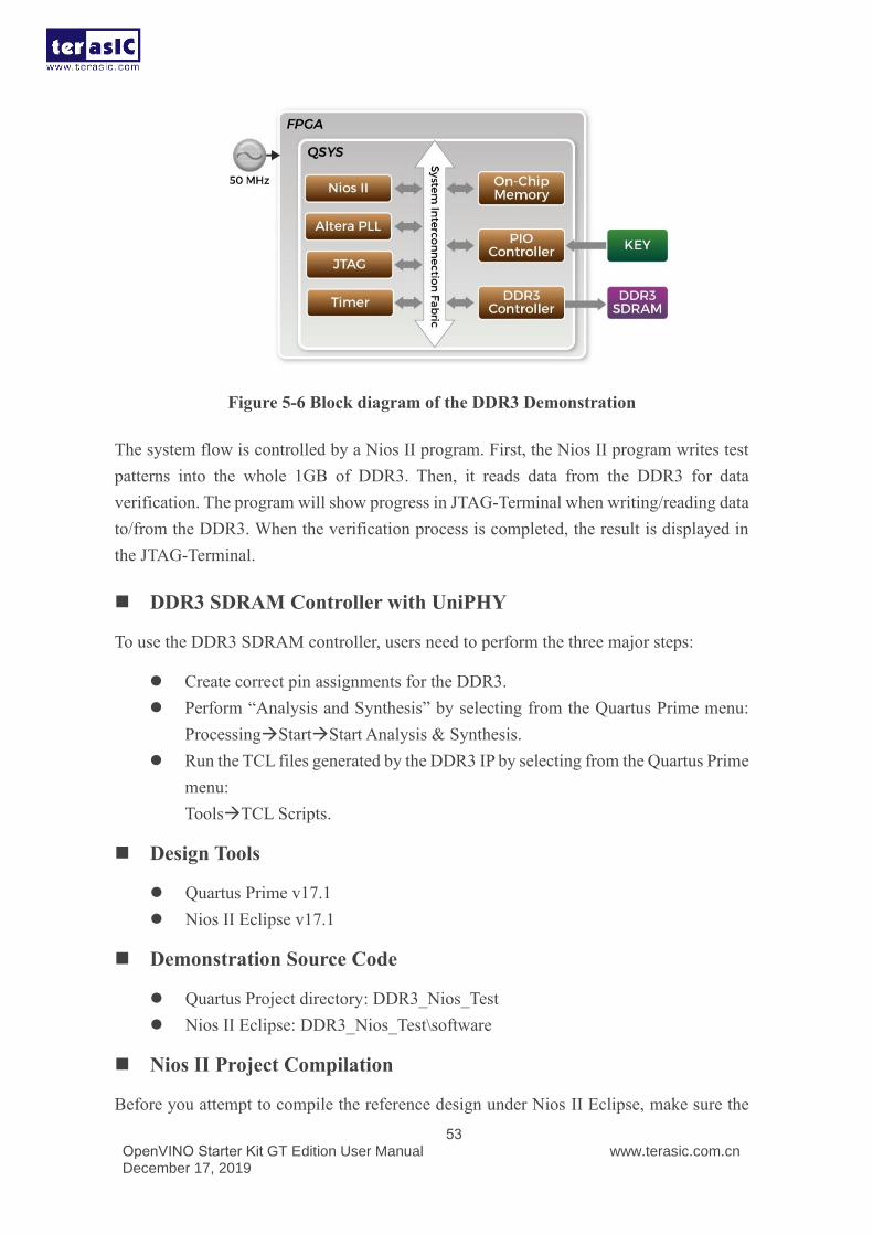
◼ System Block Diagram
Figure 5-6 shows the system block diagram of this demonstration. The system requires a
50MHz clock provided from the board. The DDR3 controller is configured as a 1GB
DDR3-400 controller with the DDR3 data rate of 800Mbps. DDR3 IP generates one
400MHz clock as DDR3’s data clock and one half-rate system clock 200MHz for those
host controllers. In the QSYS, Nios II and the On-Chip Memory are designed running with
the 100MHz clock, and the Nios II program is running in the on-chip memory.
OpenVINO Starter Kit GT Edition User Manual December 17, 2019
www.terasic.com.cn
53
Figure 5-6 Block diagram of the DDR3 Demonstration
The system flow is controlled by a Nios II program. First, the Nios II program writes test
patterns into the whole 1GB of DDR3. Then, it reads data from the DDR3 for data
verification. The program will show progress in JTAG-Terminal when writing/reading data
to/from the DDR3. When the verification process is completed, the result is displayed in
the JTAG-Terminal.
◼ DDR3 SDRAM Controller with UniPHY
To use the DDR3 SDRAM controller, users need to perform the three major steps:
⚫ Create correct pin assignments for the DDR3.
⚫ Perform “Analysis and Synthesis” by selecting from the Quartus Prime menu:
Processing→Start→Start Analysis & Synthesis.
⚫ Run the TCL files generated by the DDR3 IP by selecting from the Quartus Prime
menu:
Tools→TCL Scripts.
◼ Design Tools
⚫ Quartus Prime v17.1
⚫ Nios II Eclipse v17.1
◼ Demonstration Source Code
⚫ Quartus Project directory: DDR3_Nios_Test
⚫ Nios II Eclipse: DDR3_Nios_Test\software
◼ Nios II Project Compilation
Before you attempt to compile the reference design under Nios II Eclipse, make sure the
OpenVINO Starter Kit GT Edition User Manual December 17, 2019
www.terasic.com.cn
54
project is cleaned first by clicking “Clean” from the “Project” menu of Nios II Eclipse.
◼ Demonstration Batch File
Demo Batch File Folder:DDR3_Nios_Test\demo_batch
The demo batch file includes following files:
⚫ Batch File for USB Blaster II: test.bat, test.sh
⚫ FPGA Configure File: DDR3_Nios_Test.sof
⚫ Nios II Program: MEM_TEST.elf
◼ Demonstration Setup
⚫ Make sure the Quartus Prime v17.1、Nios II and USB-Blaster II driver are all
installed on your PC.
⚫ Use USB cable to connect PC and the OpenVINO Starter Kit GT Edition USB
Blaster II connector (J5).
⚫ Power on the OpenVINO Starter Kit GT Edition.
⚫ Execute the demo batch file “test.bat” under the batch file folder:
DDR3_Nios_Test\demo_batch.
⚫ After Nios II program is downloaded and executed successfully, a prompt
message will be displayed in nios2-terminal.
⚫ Press KEY3~KEY0 of the OpenVINO Starter Kit GT Edition to start DDR3
verify process.
OpenVINO Starter Kit GT Edition User Manual December 17, 2019
www.terasic.com.cn
55
⚫ The program will display progressing and result information, as shown in Figure
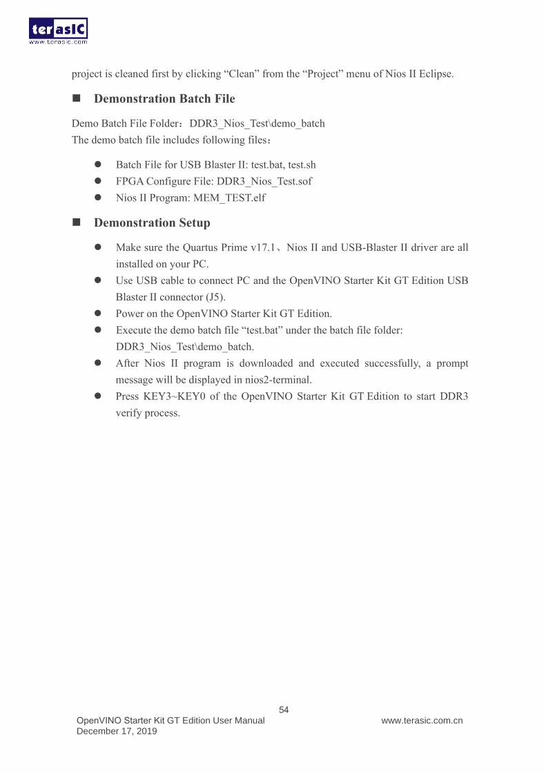
5-7.
Figure 5-7 Display Progress and Result Information for the DDR3 Demonstration
5.6 UART Control
Many applications need communication with computer through common ports, the
traditional connector is RS232 which needs to connect to a RS232 cable. But today many
personal computers don't have the RS232 connector which makes it very inconvenient to
develop projects. The OpenVINO Starter Kit GT Edition is designed to support UART
communication through the USB cable. The UART to USB circuit is responsible for
converting the data format. Developers can use a USB cable rather than a RS232 cable to
enable the communication between the FPGA and the host computer. In this demonstration
we will show you how to control the LEDs by sending a command on the computer putty
terminal. The command is sent and received through a USB cable to the FPGA. Note that
in FPGA, the information was received and sent through a UART IP.
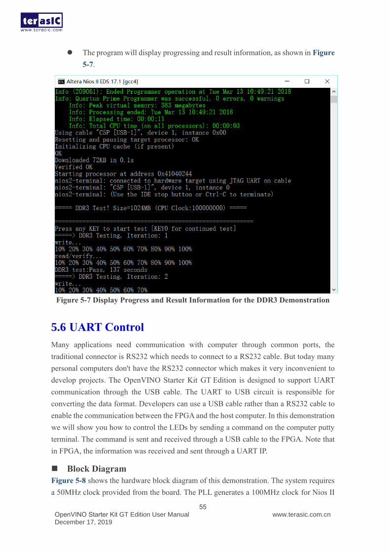
◼ Block Diagram
Figure 5-8 shows the hardware block diagram of this demonstration. The system requires
a 50MHz clock provided from the board. The PLL generates a 100MHz clock for Nios II
OpenVINO Starter Kit GT Edition User Manual December 17, 2019
www.terasic.com.cn
56
processor and the controller IP. The LEDs are controlled by the PIO IP. The UART
controller sends and receives command data and the command is sent through the Putty
terminal on the computer.
Figure 5-8 Block diagram of UART Control LED demonstration
◼ Design Tools
⚫ Quartus Prime v17.1
⚫ Nios II Eclipse v17.1
◼ Demonstration Source Code
⚫ Quartus Project Directory: UART_USB_LED
⚫ Nios II software Directory: UART_USB_LED\software
◼ Demonstration Batch File
Demo Batch File Folder:UART_USB_LED \demo_batch
The demo batch file includes following files:
⚫ Batch File:test.bat、test.sh
⚫ FPGA Configure File:UART_USB_LED.sof
⚫ Nios II Program:UART_USB_LED.elf
◼ Demonstration Setup
⚫ Connect a USB cable between your computer and the UART TO USB port (J6).
⚫ Power on the OpenVINO Starter Kit GT Edition.
⚫ Open PC Device Manager, if you find an unrecognized USB Serial Port in
OpenVINO Starter Kit GT Edition User Manual December 17, 2019
www.terasic.com.cn
57
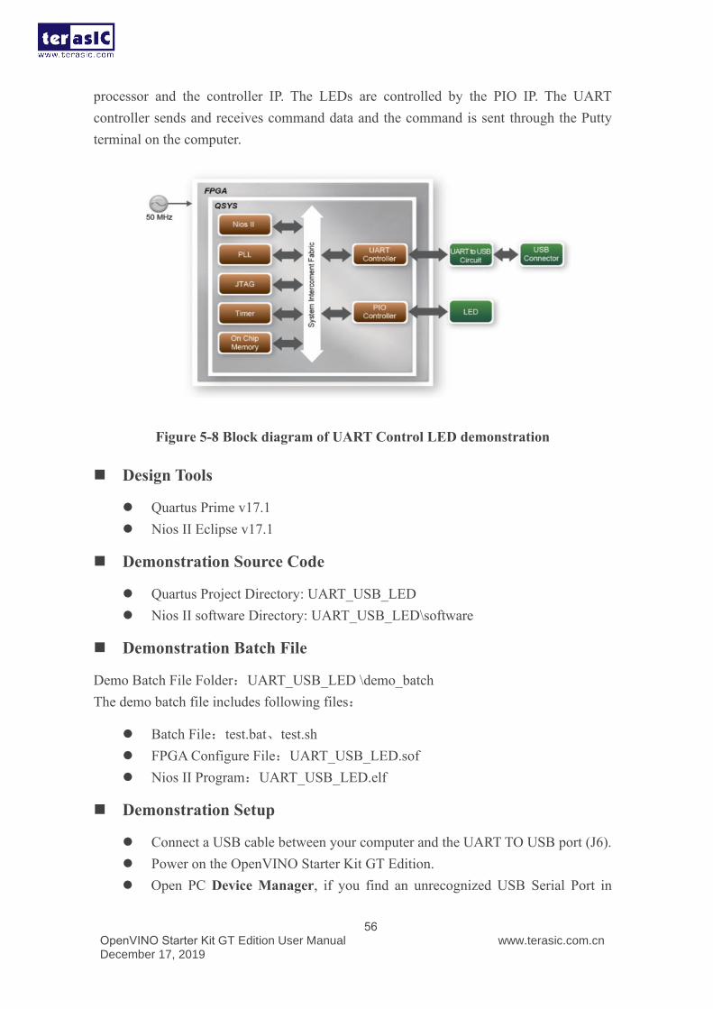
Device Manager as shown in Figure 5-9, you should install the UART to USB
driver before you run the demonstration.
The driver is located in the OpenVINO Starter Kit GT Edition System CD
directory Tool\serial_driver\, you can install the driver corresponds to your PC
operating system.
Figure 5-9 Unrecognized USB Serial Port on PC
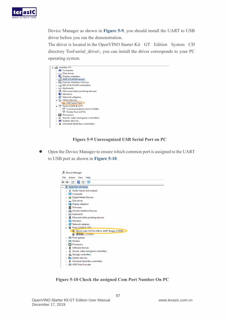
⚫ Open the Device Manager to ensure which common port is assigned to the UART
to USB port as shown in Figure 5-10.
Figure 5-10 Check the assigned Com Port Number On PC
OpenVINO Starter Kit GT Edition User Manual December 17, 2019
www.terasic.com.cn
58
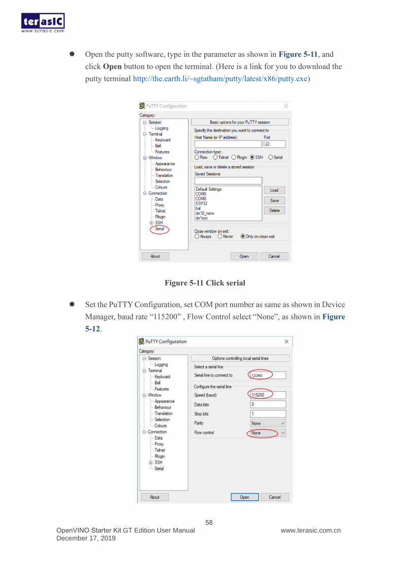
⚫ Open the putty software, type in the parameter as shown in Figure 5-11, and
click Open button to open the terminal. (Here is a link for you to download the
putty terminal http://the.earth.li/~sgtatham/putty/latest/x86/putty.exe)
Figure 5-11 Click serial
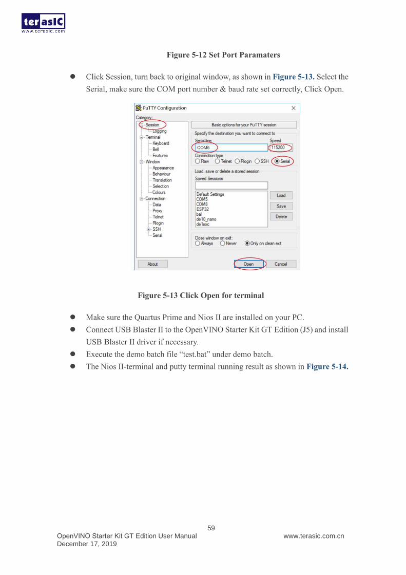
⚫ Set the PuTTY Configuration, set COM port number as same as shown in Device
Manager, baud rate “115200” , Flow Control select “None”, as shown in Figure
5-12.
OpenVINO Starter Kit GT Edition User Manual December 17, 2019
www.terasic.com.cn
59
Figure 5-12 Set Port Paramaters
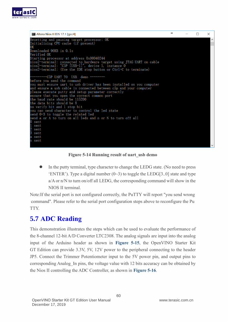
⚫ Click Session, turn back to original window, as shown in Figure 5-13. Select the
Serial, make sure the COM port number & baud rate set correctly, Click Open.
Figure 5-13 Click Open for terminal
⚫ Make sure the Quartus Prime and Nios II are installed on your PC.
⚫ Connect USB Blaster II to the OpenVINO Starter Kit GT Edition (J5) and install
USB Blaster II driver if necessary.
⚫ Execute the demo batch file “test.bat” under demo batch.
⚫ The Nios II-terminal and putty terminal running result as shown in Figure 5-14.
OpenVINO Starter Kit GT Edition User Manual December 17, 2019
www.terasic.com.cn
60
Figure 5-14 Running result of uart_usb demo
⚫ In the putty terminal, type character to change the LEDG state. (No need to press
‘ENTER’). Type a digital number (0~3) to toggle the LEDG[3..0] state and type
a/A or n/N to turn on/off all LEDG, the corresponding command will show in the
NIOS II terminal.
Note:If the serial port is not configured correctly, the PuTTY will report "you send wrong
command". Please refer to the serial port configuration steps above to reconfigure the Pu
TTY.
5.7 ADC Reading
This demonstration illustrates the steps which can be used to evaluate the performance of
the 8-channel 12-bit A/D Converter LTC2308. The analog signals are input into the analog
input of the Arduino header as shown in Figure 5-15, the OpenVINO Starter Kit
GT Edition can provide 3.3V, 5V, 12V power to the peripheral connecting to the header
JP5. Connect the Trimmer Potentiometer input to the 5V power pin, and output pins to
corresponding Analog_In pins, the voltage value with 12 bits accuracy can be obtained by
the Nios II controlling the ADC Controller, as shown in Figure 5-16.
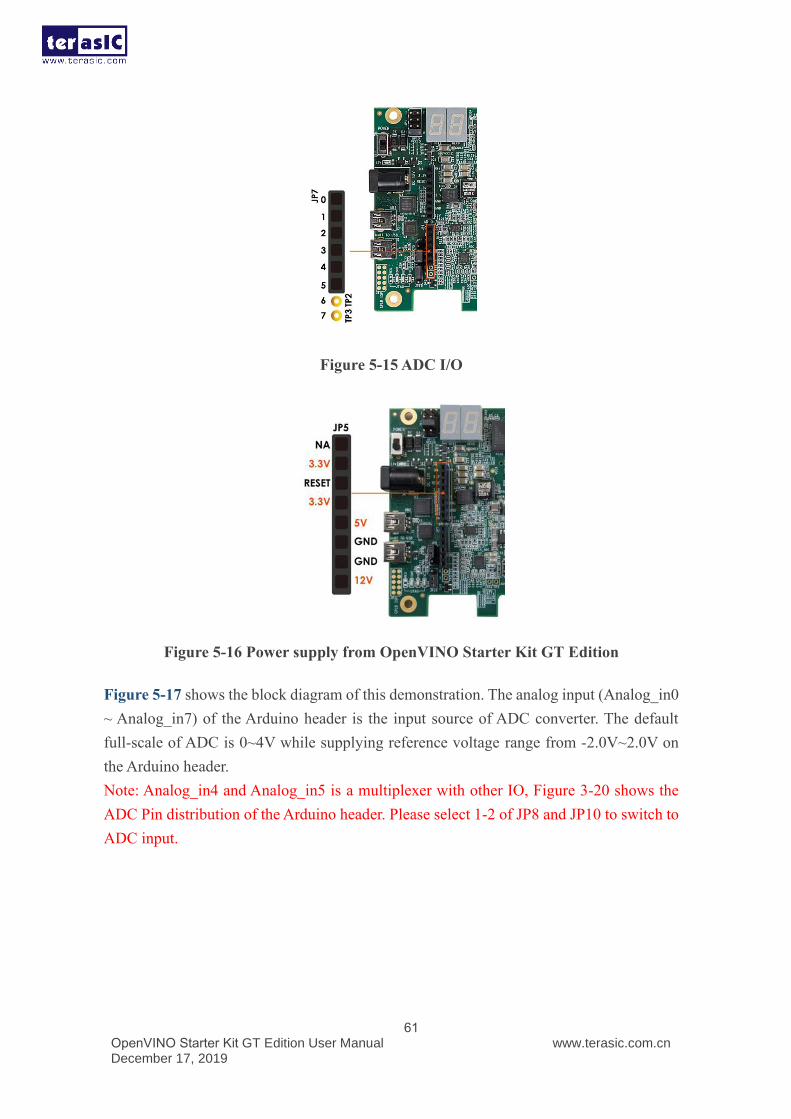
OpenVINO Starter Kit GT Edition User Manual December 17, 2019
www.terasic.com.cn
61
Figure 5-15 ADC I/O
Figure 5-16 Power supply from OpenVINO Starter Kit GT Edition
Figure 5-17 shows the block diagram of this demonstration. The analog input (Analog_in0
~ Analog_in7) of the Arduino header is the input source of ADC converter. The default
full-scale of ADC is 0~4V while supplying reference voltage range from -2.0V~2.0V on
the Arduino header.
Note: Analog_in4 and Analog_in5 is a multiplexer with other IO, Figure 3-20 shows the
ADC Pin distribution of the Arduino header. Please select 1-2 of JP8 and JP10 to switch to
ADC input.
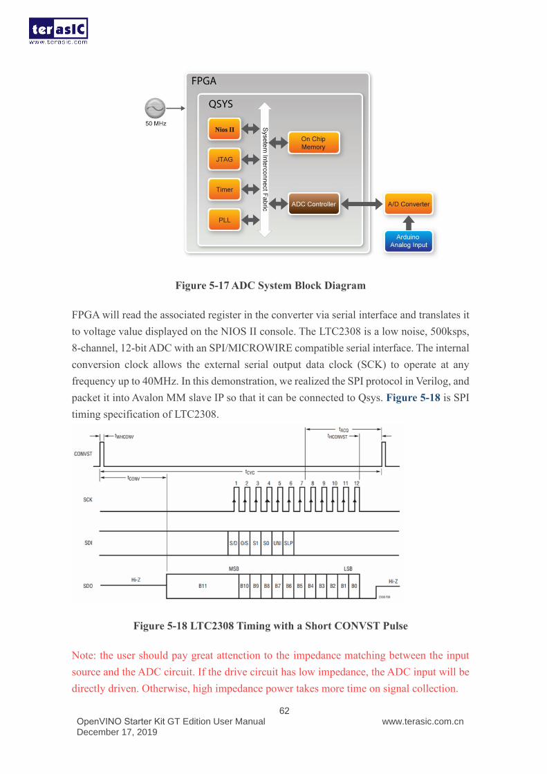
OpenVINO Starter Kit GT Edition User Manual December 17, 2019
www.terasic.com.cn
62
Figure 5-17 ADC System Block Diagram
FPGA will read the associated register in the converter via serial interface and translates it
to voltage value displayed on the NIOS II console. The LTC2308 is a low noise, 500ksps,
8-channel, 12-bit ADC with an SPI/MICROWIRE compatible serial interface. The internal
conversion clock allows the external serial output data clock (SCK) to operate at any
frequency up to 40MHz. In this demonstration, we realized the SPI protocol in Verilog, and
packet it into Avalon MM slave IP so that it can be connected to Qsys. Figure 5-18 is SPI
timing specification of LTC2308.
Figure 5-18 LTC2308 Timing with a Short CONVST Pulse
Note: the user should pay great attenction to the impedance matching between the input
source and the ADC circuit. If the drive circuit has low impedance, the ADC input will be
directly driven. Otherwise, high impedance power takes more time on signal collection.
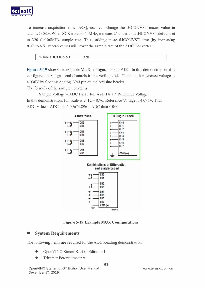
OpenVINO Starter Kit GT Edition User Manual December 17, 2019
www.terasic.com.cn
63
To increase acquisition time tACQ, user can change the tHCONVST macro value in
adc_ltc2308.v. When SCK is set to 40MHz, it means 25ns per unit. tHCONVST default set
to 320 for100MHz sample rate. Thus, adding more tHCONVST time (by increasing
tHCONVST macro value) will lower the sample rate of the ADC Converter
`define tHCONVST 320
Figure 5-19 shows the example MUX configurations of ADC. In this demonstration, it is
configured as 8 signal-end channels in the verilog code. The default reference voltage is
4.096V by floating Analog_Vref pin on the Arduino header.
The formula of the sample voltage is:
Sample Voltage = ADC Data / full scale Data * Reference Voltage.
In this demonstration, full scale is 2^12 =4096. Reference Voltage is 4.096V. Thus
ADC Value = ADC data/4096*4.096 = ADC data /1000
Figure 5-19 Example MUX Configurations
◼ System Requirements
The following items are required for the ADC Reading demonstration:
⚫ OpenVINO Starter Kit GT Edition x1
⚫ Trimmer Potentiometer x1
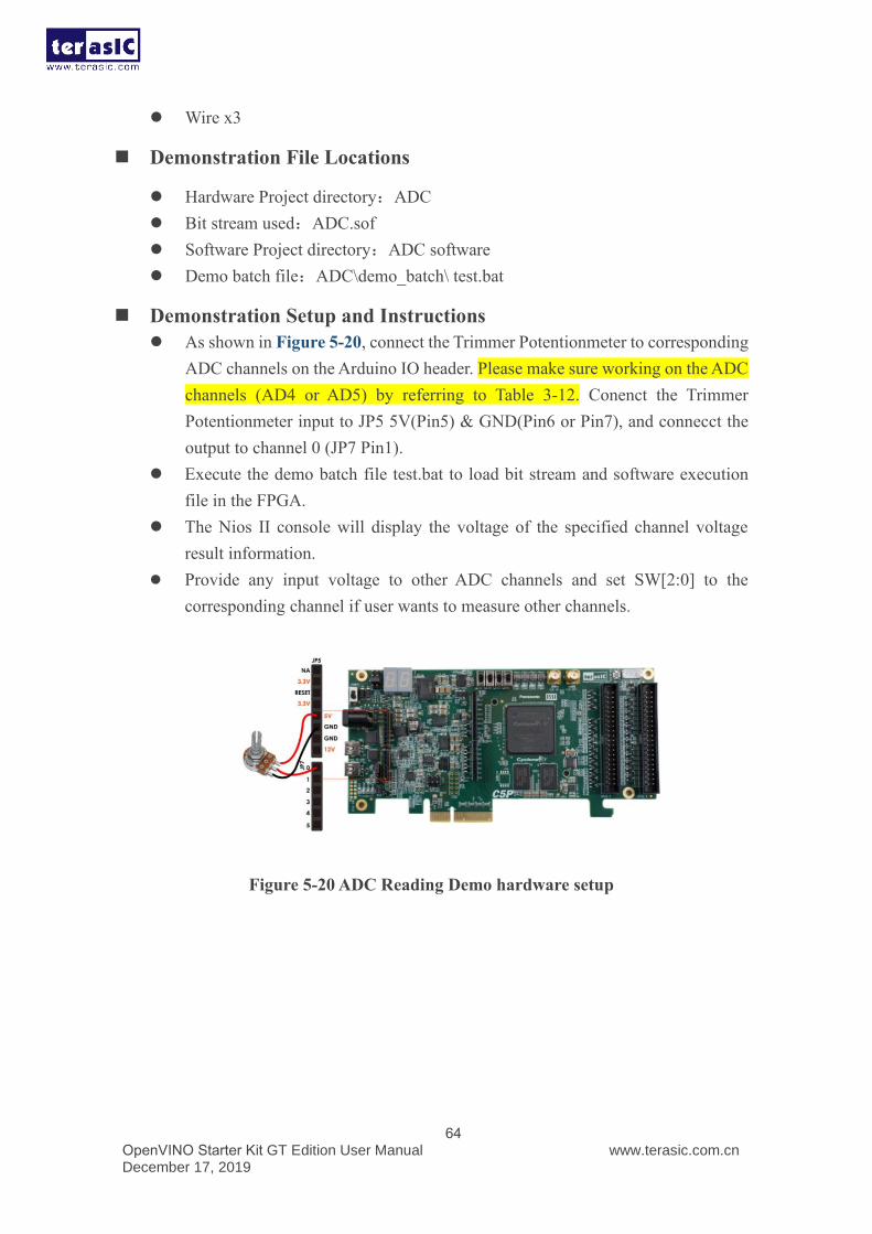
OpenVINO Starter Kit GT Edition User Manual December 17, 2019
www.terasic.com.cn
64
⚫ Wire x3
◼ Demonstration File Locations
⚫ Hardware Project directory:ADC
⚫ Bit stream used:ADC.sof
⚫ Software Project directory:ADC software
⚫ Demo batch file:ADC\demo_batch\ test.bat
◼ Demonstration Setup and Instructions
⚫ As shown in Figure 5-20, connect the Trimmer Potentionmeter to corresponding
ADC channels on the Arduino IO header. Please make sure working on the ADC
channels (AD4 or AD5) by referring to Table 3-12. Conenct the Trimmer
Potentionmeter input to JP5 5V(Pin5) & GND(Pin6 or Pin7), and connecct the
output to channel 0 (JP7 Pin1).
⚫ Execute the demo batch file test.bat to load bit stream and software execution
file in the FPGA.
⚫ The Nios II console will display the voltage of the specified channel voltage
result information.
⚫ Provide any input voltage to other ADC channels and set SW[2:0] to the
corresponding channel if user wants to measure other channels.
Figure 5-20 ADC Reading Demo hardware setup
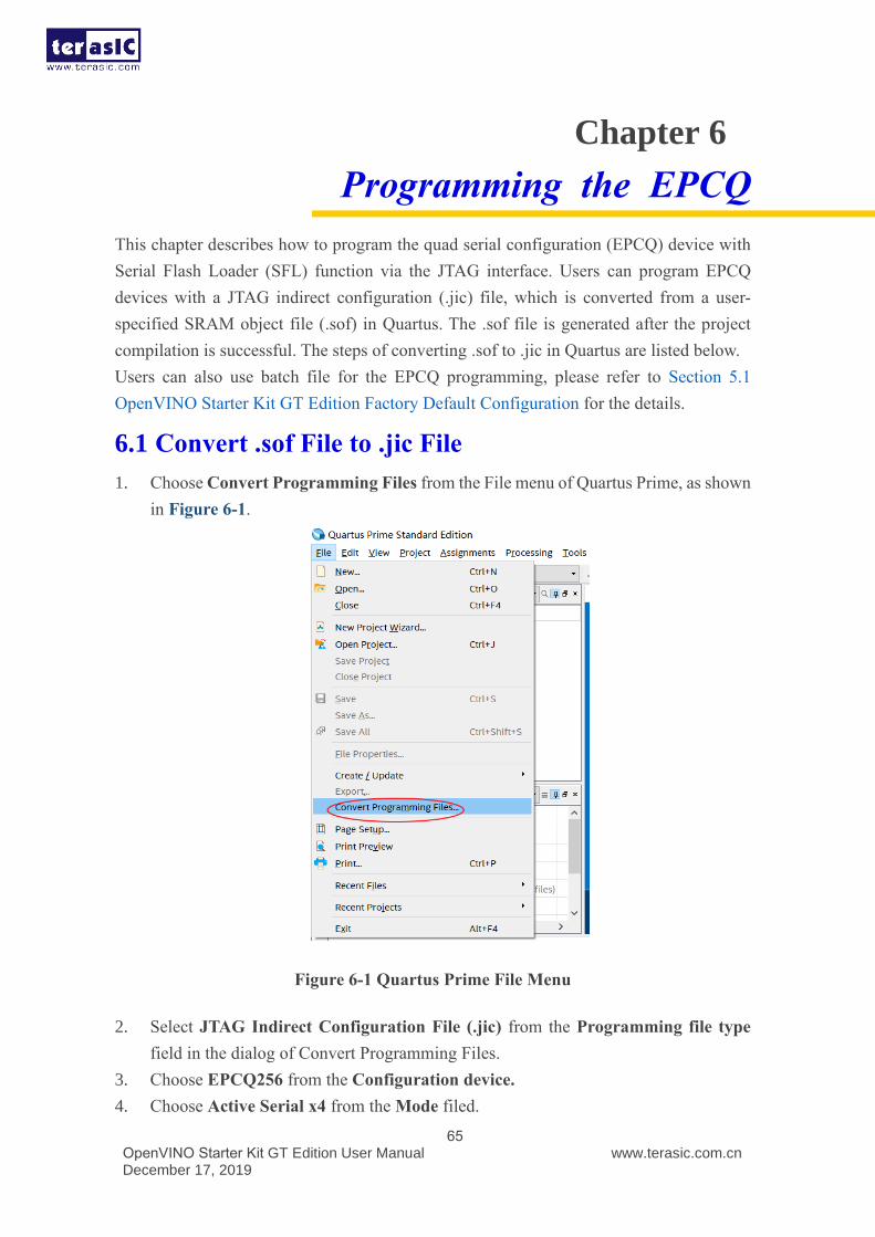
OpenVINO Starter Kit GT Edition User Manual December 17, 2019
www.terasic.com.cn
65
Chapter 6
Programming the EPCQ
This chapter describes how to program the quad serial configuration (EPCQ) device with
Serial Flash Loader (SFL) function via the JTAG interface. Users can program EPCQ
devices with a JTAG indirect configuration (.jic) file, which is converted from a user-
specified SRAM object file (.sof) in Quartus. The .sof file is generated after the project
compilation is successful. The steps of converting .sof to .jic in Quartus are listed below.
Users can also use batch file for the EPCQ programming, please refer to Section 5.1
OpenVINO Starter Kit GT Edition Factory Default Configuration for the details.
6.1 Convert .sof File to .jic File
1. Choose Convert Programming Files from the File menu of Quartus Prime, as shown
in Figure 6-1.
Figure 6-1 Quartus Prime File Menu
2. Select JTAG Indirect Configuration File (.jic) from the Programming file type
field in the dialog of Convert Programming Files.
3. Choose EPCQ256 from the Configuration device.
4. Choose Active Serial x4 from the Mode filed.
OpenVINO Starter Kit GT Edition User Manual December 17, 2019
www.terasic.com.cn
66
5. Browse to the target directory from the File name field and specify the name of output
file.
6. Click on the SOF data in the section of Input files to convert, as shown in Figure
6-2.
Figure 6-2 Dialog of “Convert Programming File”
7. Click Add File.
8. Select the .sof to be converted to a .jic file from the Open File dialog.
9. Click Open.
10. Click on the Flash Loader and click Add Device, as shown in Figure 6-3.
11. Click OK and the Select Devices page will appear.
OpenVINO Starter Kit GT Edition User Manual December 17, 2019
www.terasic.com.cn
67
Figure 6-3 Click on the “Flash Loader”
12. As shown in Figure 6-4, choose the same FPGA device to with the SOF Data.
13. Click OK and the Convert Programming Files will appear,as shown in Figure 6-5.
14. Click Generate,the .jic file will be generated in the seleted directory.
Figure 6-4 Select Devices page
OpenVINO Starter Kit GT Edition User Manual December 17, 2019
www.terasic.com.cn
68
Figure 6-5 Convert Programming Files page
6.2 Write a .jic File to the EPCQ
When the conversion of SOF-to-JIC file is complete, please follow the steps below to
program the EPCQ device with the .jic file created in Quartus Prime Programmer.
1. In Quartus Prime Tools menu, choose Programmer from the Tools menu and the
Chain.cdf window will appear.
2. Click Auto Detect and then select the correct device. The FPGA device should be
detected, as shown in Figure 6-6.
3. Double click the red rectangle region, as shown in Figure 6-6 and the Select New
Programming File page will appear. Select the .jic file to be programmed.
4. Program the EPCQ device by clicking the corresponding Program/Configure box. A
factory default SFL image will be loaded, as shown in Figure 6-7.
5. Click Start to program the EPCQ device.
OpenVINO Starter Kit GT Edition User Manual December 17, 2019
www.terasic.com.cn
69
Figure 6-6 Quartus Prime Programmer detectes the FPGA device
Figure 6-7 Quartus Prime Programmer window with .jic file
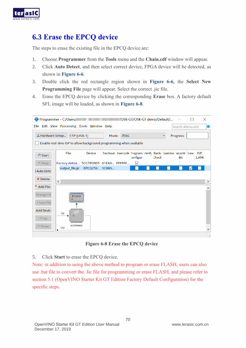
OpenVINO Starter Kit GT Edition User Manual December 17, 2019
www.terasic.com.cn
70
6.3 Erase the EPCQ device
The steps to erase the existing file in the EPCQ device are:
1. Choose Programmer from the Tools menu and the Chain.cdf window will appear.
2. Click Auto Detect, and then select correct device, FPGA device will be detected, as
shown in Figure 6-6.
3. Double click the red rectangle region shown in Figure 6-6, the Select New
Programming File page will appear. Select the correct .jic file.
4. Erase the EPCQ device by clicking the corresponding Erase box. A factory default
SFL image will be loaded, as shown in Figure 6-8.
Figure 6-8 Erase the EPCQ device
5. Click Start to erase the EPCQ device.
Note: in addition to using the above method to program or erase FLASH, users can also
use .bat file to convert the. Jic file for programming or erase FLASH, and please refer to
section 5.1 (OpenVINO Starter Kit GT Edition Factory Default Configuration) for the
specific steps.
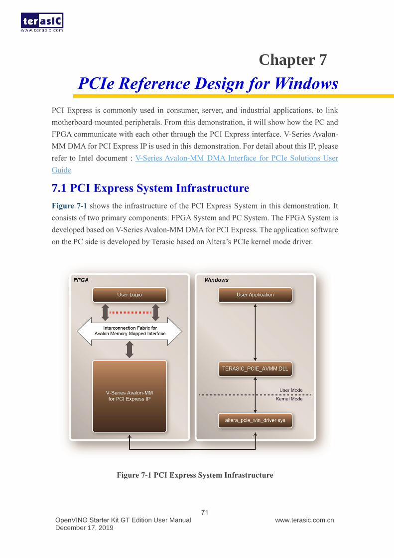
OpenVINO Starter Kit GT Edition User Manual December 17, 2019
www.terasic.com.cn
71
Chapter 7
PCIe Reference Design for Windows
PCI Express is commonly used in consumer, server, and industrial applications, to link
motherboard-mounted peripherals. From this demonstration, it will show how the PC and
FPGA communicate with each other through the PCI Express interface. V-Series Avalon-
MM DMA for PCI Express IP is used in this demonstration. For detail about this IP, please
refer to Intel document : V-Series Avalon-MM DMA Interface for PCIe Solutions User
Guide
7.1 PCI Express System Infrastructure
Figure 7-1 shows the infrastructure of the PCI Express System in this demonstration. It
consists of two primary components: FPGA System and PC System. The FPGA System is
developed based on V-Series Avalon-MM DMA for PCI Express. The application software
on the PC side is developed by Terasic based on Altera’s PCIe kernel mode driver.
Figure 7-1 PCI Express System Infrastructure
OpenVINO Starter Kit GT Edition User Manual December 17, 2019
www.terasic.com.cn
72
7.2 PCI Express Software SDK
The FPGA System CD contains a PC Windows based SDK to allow users to develop their
64-bits software application on Windows XP/7/10 64-bits. The SDK is located in the “CD
ROM\Demonstration\PCIe_SW_KIT\Windows” folder which includes:
⚫ PCI Express Driver
⚫ PCI Express Library
⚫ PCI Express Examples
The kernel mode driver assumes the PCIe vender ID (VID) is 0x1172 and the device ID
(DID) is 0xE001. If different VID and DID are used in the design, users need to modify
the PCIe vender ID (VID) and device ID (DID) in the driver INF file accordingly.
The PCI Express Library is implemented as a single DLL called
TERASIC_PCIE_AVMM.dll. This file is a 64-bits DLL. With the DLL exported to the
software API, users can easily communicate with the FPGA. The library provides the
following functions:
⚫ Basic Data Read and Write
⚫ Data Read and Write by DMA
For high performance data transmission, DMA is required as the read and write operations
are specified under the hardware design on the FPGA.
7.3 PCI Express Software Stack
Figure 7-2 shows the software stack for the PCI Express application software on 64-bit
Windows. The PCI Express driver incorporated in the DLL library is called
TERASIC_PCIE_AVMM.dll. Users can develop their applications based on this DLL. The
altera_pcie_win_driver.sys kernel driver is provided by Intel.
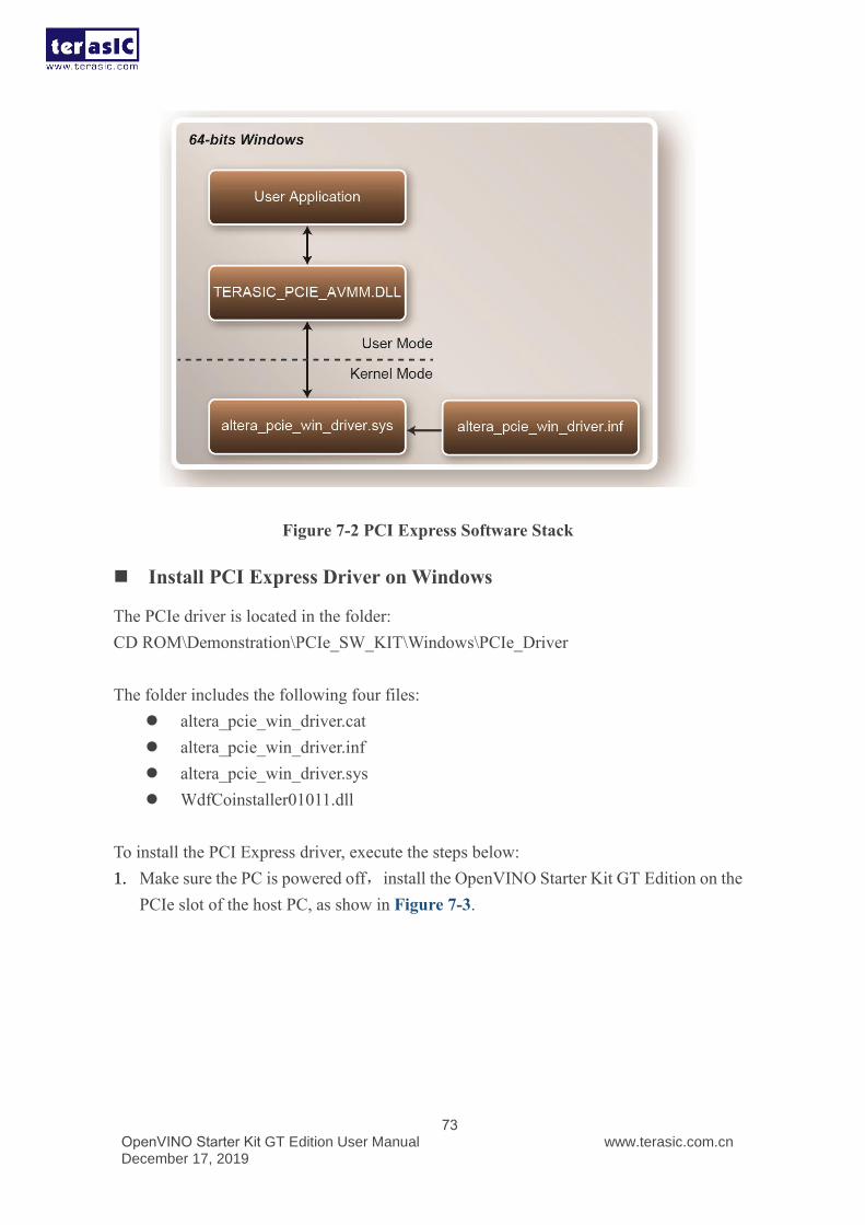
OpenVINO Starter Kit GT Edition User Manual December 17, 2019
www.terasic.com.cn
73
Figure 7-2 PCI Express Software Stack
◼ Install PCI Express Driver on Windows
The PCIe driver is located in the folder:
CD ROM\Demonstration\PCIe_SW_KIT\Windows\PCIe_Driver
The folder includes the following four files:
⚫ altera_pcie_win_driver.cat
⚫ altera_pcie_win_driver.inf
⚫ altera_pcie_win_driver.sys
⚫ WdfCoinstaller01011.dll
To install the PCI Express driver, execute the steps below:
1. Make sure the PC is powered off,install the OpenVINO Starter Kit GT Edition on the
PCIe slot of the host PC, as show in Figure 7-3.
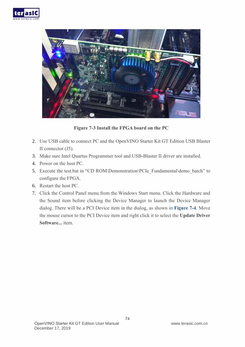
OpenVINO Starter Kit GT Edition User Manual December 17, 2019
www.terasic.com.cn
74
Figure 7-3 Install the FPGA board on the PC
2. Use USB cable to connect PC and the OpenVINO Starter Kit GT Edition USB Blaster
II connector (J5).
3. Make sure Intel Quartus Programmer tool and USB-Blaster II driver are installed.
4. Power on the host PC.
5. Execute the test.bat in “CD ROM\Demonstration\PCIe_Fundamental\demo_batch” to
configure the FPGA.
6. Restart the host PC.
7. Click the Control Panel menu from the Windows Start menu. Click the Hardware and
the Sound item before clicking the Device Manager to launch the Device Manager
dialog. There will be a PCI Device item in the dialog, as shown in Figure 7-4. Move
the mouse cursor to the PCI Device item and right click it to select the Update Driver
Software... item.
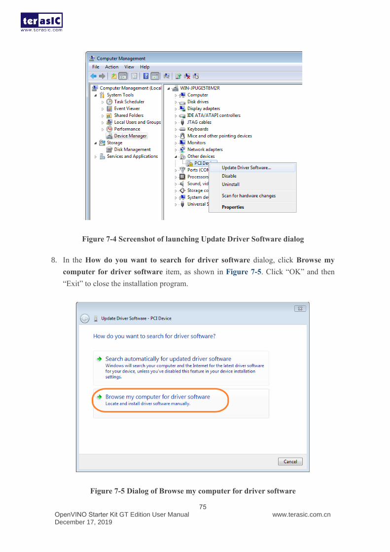
OpenVINO Starter Kit GT Edition User Manual December 17, 2019
www.terasic.com.cn
75
Figure 7-4 Screenshot of launching Update Driver Software dialog
8. In the How do you want to search for driver software dialog, click Browse my
computer for driver software item, as shown in Figure 7-5. Click “OK” and then
“Exit” to close the installation program.
Figure 7-5 Dialog of Browse my computer for driver software
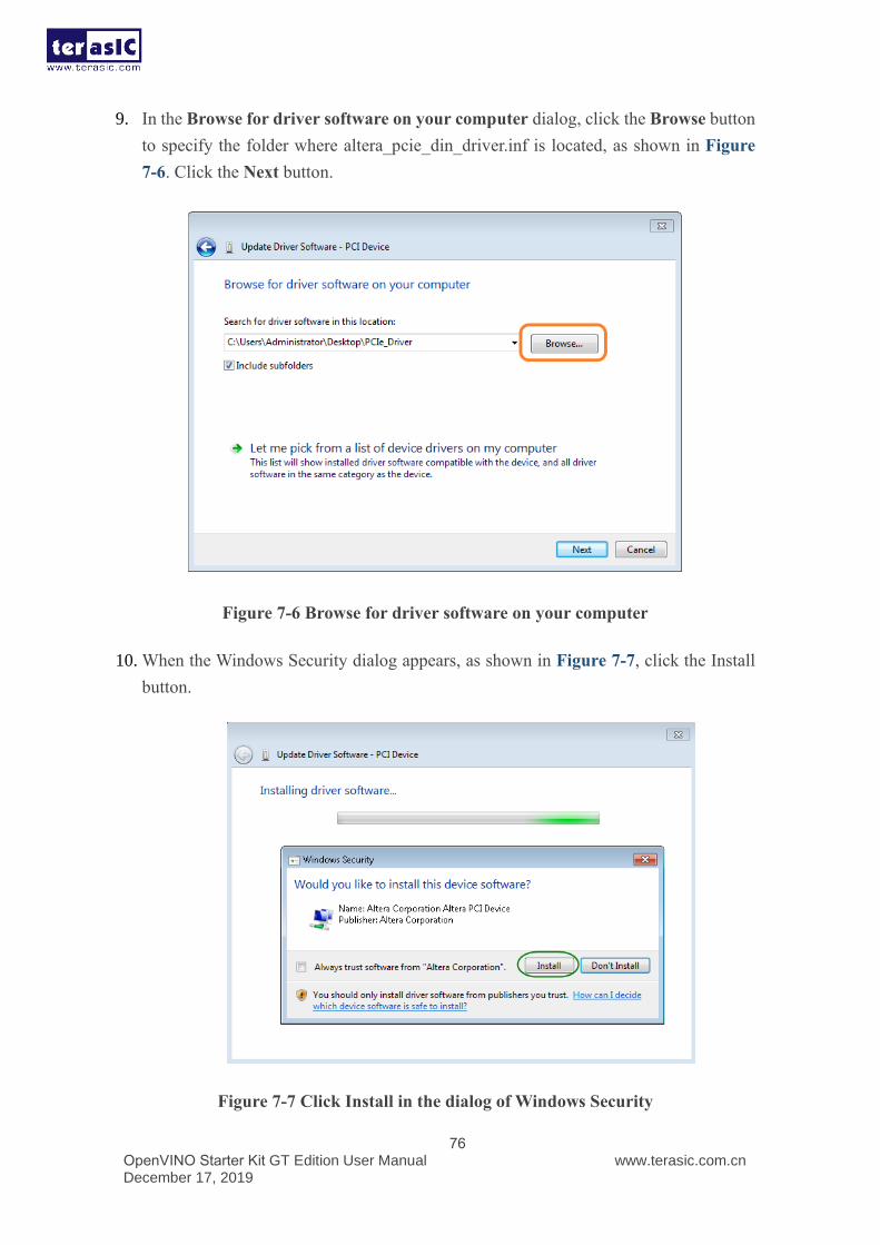
OpenVINO Starter Kit GT Edition User Manual December 17, 2019
www.terasic.com.cn
76
9. In the Browse for driver software on your computer dialog, click the Browse button
to specify the folder where altera_pcie_din_driver.inf is located, as shown in Figure
7-6. Click the Next button.
Figure 7-6 Browse for driver software on your computer
10. When the Windows Security dialog appears, as shown in Figure 7-7, click the Install
button.
Figure 7-7 Click Install in the dialog of Windows Security
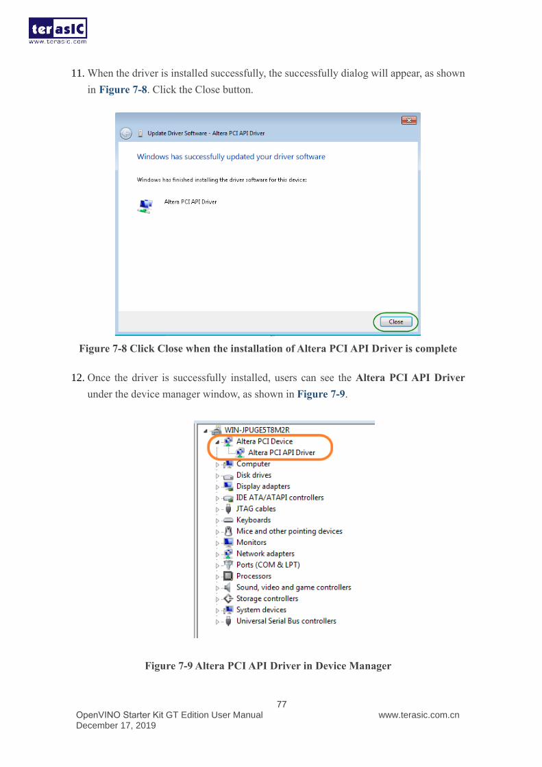
OpenVINO Starter Kit GT Edition User Manual December 17, 2019
www.terasic.com.cn
77
11. When the driver is installed successfully, the successfully dialog will appear, as shown
in Figure 7-8. Click the Close button.
Figure 7-8 Click Close when the installation of Altera PCI API Driver is complete
12. Once the driver is successfully installed, users can see the Altera PCI API Driver
under the device manager window, as shown in Figure 7-9.
Figure 7-9 Altera PCI API Driver in Device Manager
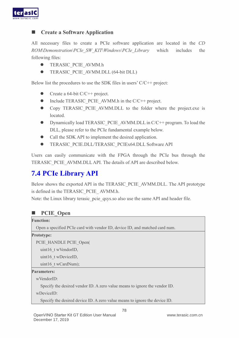
OpenVINO Starter Kit GT Edition User Manual December 17, 2019
www.terasic.com.cn
78
◼ Create a Software Application
All necessary files to create a PCIe software application are located in the CD
ROM\Demonstration\PCIe_SW_KIT\Windows\PCIe_Library which includes the
following files:
⚫ TERASIC_PCIE_AVMM.h
⚫ TERASIC_PCIE_AVMM.DLL (64-bit DLL)
Below list the procedures to use the SDK files in users’ C/C++ project:
⚫ Create a 64-bit C/C++ project.
⚫ Include TERASIC_PCIE_AVMM.h in the C/C++ project.
⚫ Copy TERASIC_PCIE_AVMM.DLL to the folder where the project.exe is
located.
⚫ Dynamically load TERASIC_PCIE_AVMM.DLL in C/C++ program. To load the
DLL, please refer to the PCIe fundamental example below.
⚫ Call the SDK API to implement the desired application.
⚫ TERASIC_PCIE.DLL/TERASIC_PCIEx64.DLL Software API
Users can easily communicate with the FPGA through the PCIe bus through the
TERASIC_PCIE_AVMM.DLL API. The details of API are described below.
7.4 PCIe Library API
Below shows the exported API in the TERASIC_PCIE_AVMM.DLL. The API prototype
is defined in the TERASIC_PCIE_ AVMM.h.
Note: the Linux library terasic_pcie_qsys.so also use the same API and header file.
◼ PCIE_Open
Function:
Open a specified PCIe card with vendor ID, device ID, and matched card num.
Prototype:
PCIE_HANDLE PCIE_Open(
uint16_t wVendorID,
uint16_t wDeviceID,
uint16_t wCardNum);
Parameters:
wVendorID:
Specify the desired vendor ID. A zero value means to ignore the vendor ID.
wDeviceID:
Specify the desired device ID. A zero value means to ignore the device ID.
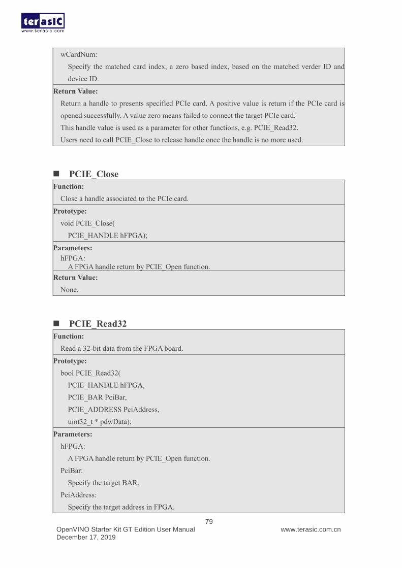
OpenVINO Starter Kit GT Edition User Manual December 17, 2019
www.terasic.com.cn
79
wCardNum:
Specify the matched card index, a zero based index, based on the matched verder ID and
device ID.
Return Value:
Return a handle to presents specified PCIe card. A positive value is return if the PCIe card is
opened successfully. A value zero means failed to connect the target PCIe card.
This handle value is used as a parameter for other functions, e.g. PCIE_Read32.
Users need to call PCIE_Close to release handle once the handle is no more used.
◼ PCIE_Close
Function:
Close a handle associated to the PCIe card.
Prototype:
void PCIE_Close(
PCIE_HANDLE hFPGA);
Parameters:
hFPGA:
A FPGA handle return by PCIE_Open function.
Return Value:
None.
◼ PCIE_Read32
Function:
Read a 32-bit data from the FPGA board.
Prototype:
bool PCIE_Read32(
PCIE_HANDLE hFPGA,
PCIE_BAR PciBar,
PCIE_ADDRESS PciAddress,
uint32_t * pdwData);
Parameters:
hFPGA:
A FPGA handle return by PCIE_Open function.
PciBar:
Specify the target BAR.
PciAddress:
Specify the target address in FPGA.
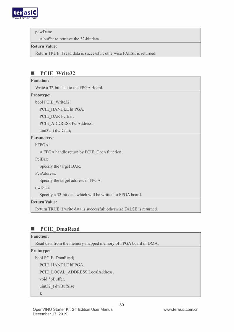
OpenVINO Starter Kit GT Edition User Manual December 17, 2019
www.terasic.com.cn
80
pdwData:
A buffer to retrieve the 32-bit data.
Return Value:
Return TRUE if read data is successful; otherwise FALSE is returned.
◼ PCIE_Write32
Function:
Write a 32-bit data to the FPGA Board.
Prototype:
bool PCIE_Write32(
PCIE_HANDLE hFPGA,
PCIE_BAR PciBar,
PCIE_ADDRESS PciAddress,
uint32_t dwData);
Parameters:
hFPGA:
A FPGA handle return by PCIE_Open function.
PciBar:
Specify the target BAR.
PciAddress:
Specify the target address in FPGA.
dwData:
Specify a 32-bit data which will be written to FPGA board.
Return Value:
Return TRUE if write data is successful; otherwise FALSE is returned.
◼ PCIE_DmaRead
Function:
Read data from the memory-mapped memory of FPGA board in DMA.
Prototype:
bool PCIE_DmaRead(
PCIE_HANDLE hFPGA,
PCIE_LOCAL_ADDRESS LocalAddress,
void *pBuffer,
uint32_t dwBufSize
);
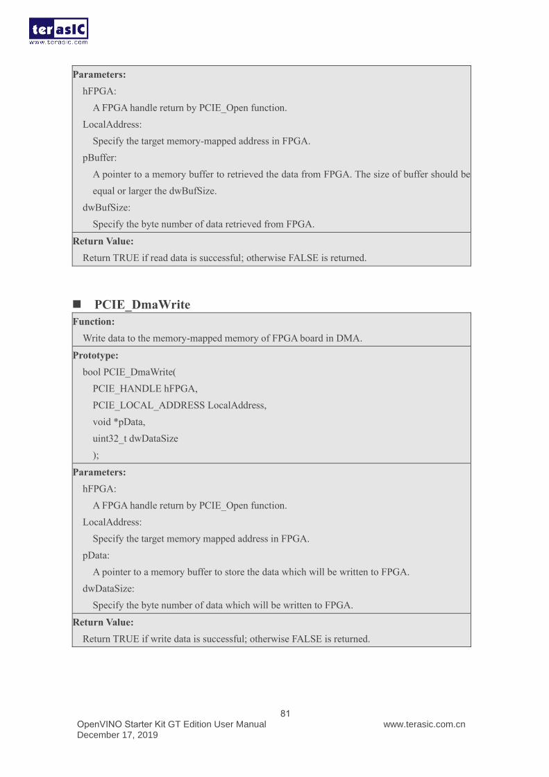
OpenVINO Starter Kit GT Edition User Manual December 17, 2019
www.terasic.com.cn
81
Parameters:
hFPGA:
A FPGA handle return by PCIE_Open function.
LocalAddress:
Specify the target memory-mapped address in FPGA.
pBuffer:
A pointer to a memory buffer to retrieved the data from FPGA. The size of buffer should be
equal or larger the dwBufSize.
dwBufSize:
Specify the byte number of data retrieved from FPGA.
Return Value:
Return TRUE if read data is successful; otherwise FALSE is returned.
◼ PCIE_DmaWrite
Function:
Write data to the memory-mapped memory of FPGA board in DMA.
Prototype:
bool PCIE_DmaWrite(
PCIE_HANDLE hFPGA,
PCIE_LOCAL_ADDRESS LocalAddress,
void *pData,
uint32_t dwDataSize
);
Parameters:
hFPGA:
A FPGA handle return by PCIE_Open function.
LocalAddress:
Specify the target memory mapped address in FPGA.
pData:
A pointer to a memory buffer to store the data which will be written to FPGA.
dwDataSize:
Specify the byte number of data which will be written to FPGA.
Return Value:
Return TRUE if write data is successful; otherwise FALSE is returned.
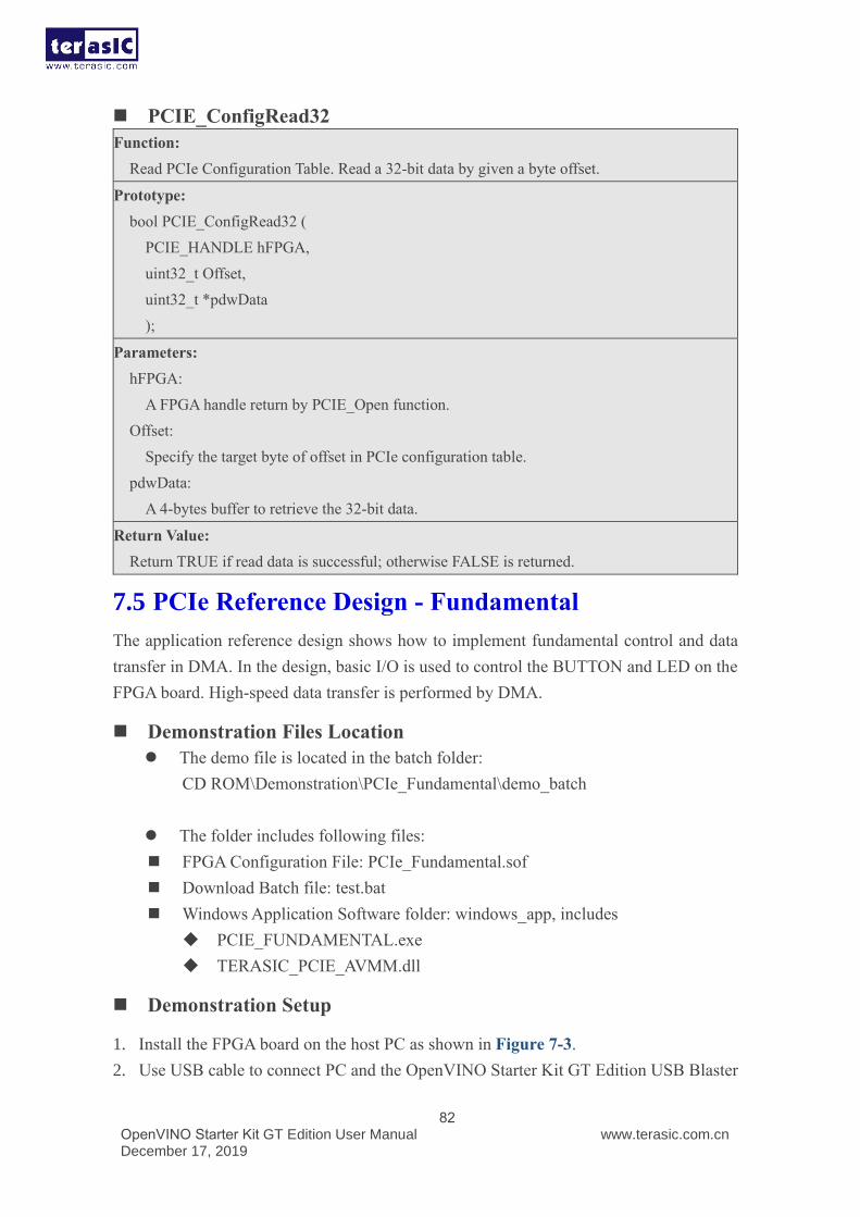
OpenVINO Starter Kit GT Edition User Manual December 17, 2019
www.terasic.com.cn
82
◼ PCIE_ConfigRead32
Function:
Read PCIe Configuration Table. Read a 32-bit data by given a byte offset.
Prototype:
bool PCIE_ConfigRead32 (
PCIE_HANDLE hFPGA,
uint32_t Offset,
uint32_t *pdwData
);
Parameters:
hFPGA:
A FPGA handle return by PCIE_Open function.
Offset:
Specify the target byte of offset in PCIe configuration table.
pdwData:
A 4-bytes buffer to retrieve the 32-bit data.
Return Value:
Return TRUE if read data is successful; otherwise FALSE is returned.
7.5 PCIe Reference Design - Fundamental
The application reference design shows how to implement fundamental control and data
transfer in DMA. In the design, basic I/O is used to control the BUTTON and LED on the
FPGA board. High-speed data transfer is performed by DMA.
◼ Demonstration Files Location
⚫ The demo file is located in the batch folder:
CD ROM\Demonstration\PCIe_Fundamental\demo_batch
⚫ The folder includes following files:
◼ FPGA Configuration File: PCIe_Fundamental.sof
◼ Download Batch file: test.bat
◼ Windows Application Software folder: windows_app, includes
◆ PCIE_FUNDAMENTAL.exe
◆ TERASIC_PCIE_AVMM.dll
◼ Demonstration Setup
1. Install the FPGA board on the host PC as shown in Figure 7-3.
2. Use USB cable to connect PC and the OpenVINO Starter Kit GT Edition USB Blaster
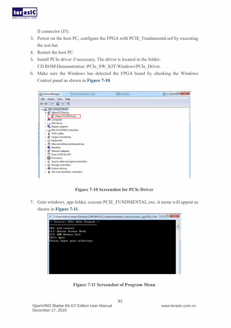
OpenVINO Starter Kit GT Edition User Manual December 17, 2019
www.terasic.com.cn
83
II connector (J5).
3. Power on the host PC, configure the FPGA with PCIE_Fundamental.sof by executing
the test.bat.
4. Restart the host PC.
5. Install PCIe driver if necessary. The driver is located in the folder:
CD ROM\Demonstration \PCIe_SW_KIT\Windows\PCIe_Driver.
6. Make sure the Windows has detected the FPGA board by checking the Windows
Control panel as shown in Figure 7-10.
Figure 7-10 Screenshot for PCIe Driver
7. Goto windows_app folder, execute PCIE_FUNDMENTAL.exe. A menu will appear as
shown in Figure 7-11.
Figure 7-11 Screenshot of Program Menu
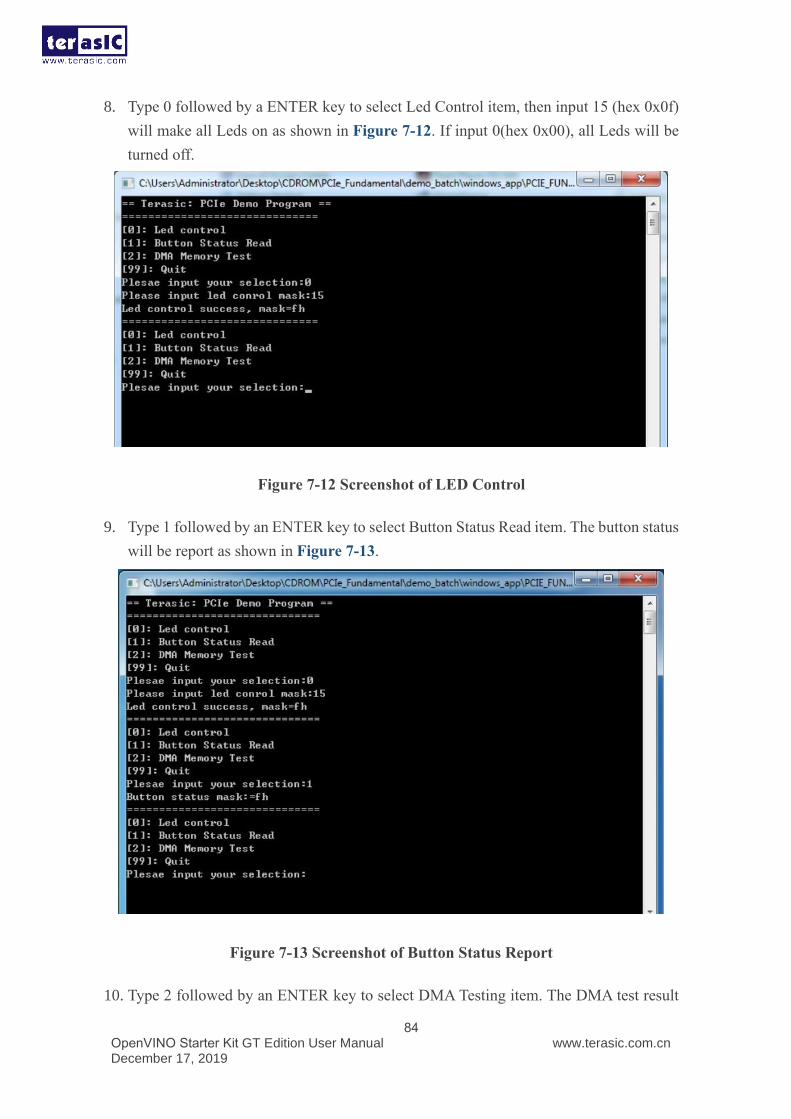
OpenVINO Starter Kit GT Edition User Manual December 17, 2019
www.terasic.com.cn
84
8. Type 0 followed by a ENTER key to select Led Control item, then input 15 (hex 0x0f)
will make all Leds on as shown in Figure 7-12. If input 0(hex 0x00), all Leds will be
turned off.
Figure 7-12 Screenshot of LED Control
9. Type 1 followed by an ENTER key to select Button Status Read item. The button status
will be report as shown in Figure 7-13.
Figure 7-13 Screenshot of Button Status Report
10. Type 2 followed by an ENTER key to select DMA Testing item. The DMA test result
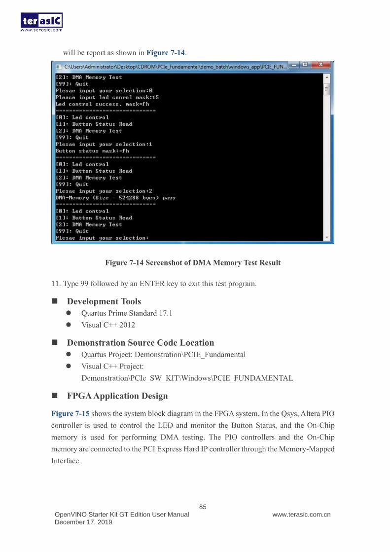
OpenVINO Starter Kit GT Edition User Manual December 17, 2019
www.terasic.com.cn
85
will be report as shown in Figure 7-14.
Figure 7-14 Screenshot of DMA Memory Test Result
11. Type 99 followed by an ENTER key to exit this test program.
◼ Development Tools
⚫ Quartus Prime Standard 17.1
⚫ Visual C++ 2012
◼ Demonstration Source Code Location
⚫ Quartus Project: Demonstration\PCIE_Fundamental
⚫ Visual C++ Project:
Demonstration\PCIe_SW_KIT\Windows\PCIE_FUNDAMENTAL
◼ FPGA Application Design
Figure 7-15 shows the system block diagram in the FPGA system. In the Qsys, Altera PIO
controller is used to control the LED and monitor the Button Status, and the On-Chip
memory is used for performing DMA testing. The PIO controllers and the On-Chip
memory are connected to the PCI Express Hard IP controller through the Memory-Mapped
Interface.
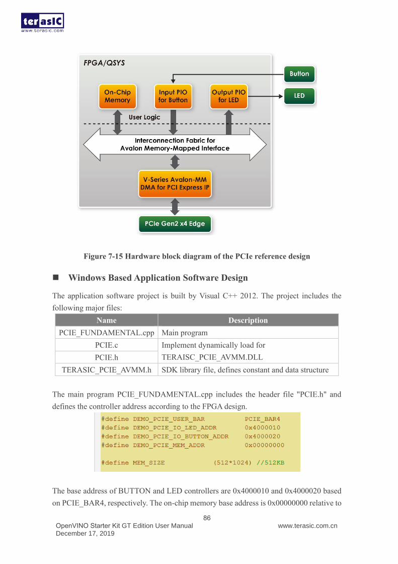
OpenVINO Starter Kit GT Edition User Manual December 17, 2019
www.terasic.com.cn
86
Figure 7-15 Hardware block diagram of the PCIe reference design
◼ Windows Based Application Software Design
The application software project is built by Visual C++ 2012. The project includes the
following major files:
Name Description
PCIE_FUNDAMENTAL.cpp Main program
PCIE.c Implement dynamically load for
TERAISC_PCIE_AVMM.DLL PCIE.h
TERASIC_PCIE_AVMM.h SDK library file, defines constant and data structure
The main program PCIE_FUNDAMENTAL.cpp includes the header file "PCIE.h" and
defines the controller address according to the FPGA design.
The base address of BUTTON and LED controllers are 0x4000010 and 0x4000020 based
on PCIE_BAR4, respectively. The on-chip memory base address is 0x00000000 relative to
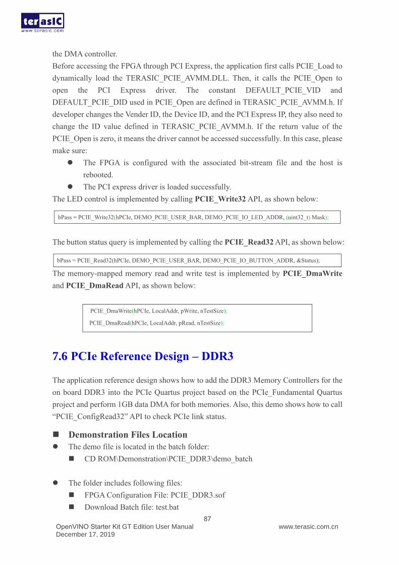
OpenVINO Starter Kit GT Edition User Manual December 17, 2019
www.terasic.com.cn
87
the DMA controller.
Before accessing the FPGA through PCI Express, the application first calls PCIE_Load to
dynamically load the TERASIC_PCIE_AVMM.DLL. Then, it calls the PCIE_Open to
open the PCI Express driver. The constant DEFAULT_PCIE_VID and
DEFAULT_PCIE_DID used in PCIE_Open are defined in TERASIC_PCIE_AVMM.h. If
developer changes the Vender ID, the Device ID, and the PCI Express IP, they also need to
change the ID value defined in TERASIC_PCIE_AVMM.h. If the return value of the
PCIE_Open is zero, it means the driver cannot be accessed successfully. In this case, please
make sure:
⚫ The FPGA is configured with the associated bit-stream file and the host is
rebooted.
⚫ The PCI express driver is loaded successfully.
The LED control is implemented by calling PCIE_Write32 API, as shown below:
bPass = PCIE_Write32(hPCIe, DEMO_PCIE_USER_BAR, DEMO_PCIE_IO_LED_ADDR, (uint32_t) Mask);
The button status query is implemented by calling the PCIE_Read32 API, as shown below:
bPass = PCIE_Read32(hPCIe, DEMO_PCIE_USER_BAR, DEMO_PCIE_IO_BUTTON_ADDR, &Status);
The memory-mapped memory read and write test is implemented by PCIE_DmaWrite
and PCIE_DmaRead API, as shown below:
7.6 PCIe Reference Design – DDR3
The application reference design shows how to add the DDR3 Memory Controllers for the
on board DDR3 into the PCIe Quartus project based on the PCIe_Fundamental Quartus
project and perform 1GB data DMA for both memories. Also, this demo shows how to call
“PCIE_ConfigRead32” API to check PCIe link status.
◼ Demonstration Files Location
⚫ The demo file is located in the batch folder:
◼ CD ROM\Demonstration\PCIE_DDR3\demo_batch
⚫ The folder includes following files:
◼ FPGA Configuration File: PCIE_DDR3.sof
◼ Download Batch file: test.bat
PCIE_DmaWrite(hPCIe, LocalAddr, pWrite, nTestSize);
PCIE_DmaRead(hPCIe, LocalAddr, pRead, nTestSize);
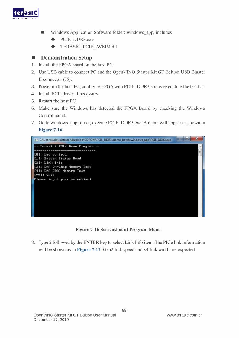
OpenVINO Starter Kit GT Edition User Manual December 17, 2019
www.terasic.com.cn
88
◼ Windows Application Software folder: windows_app, includes
◆ PCIE_DDR3.exe
◆ TERASIC_PCIE_AVMM.dll
◼ Demonstration Setup
1. Install the FPGA board on the host PC.
2. Use USB cable to connect PC and the OpenVINO Starter Kit GT Edition USB Blaster
II connector (J5).
3. Power on the host PC, configure FPGA with PCIE_DDR3.sof by executing the test.bat.
4. Install PCIe driver if necessary.
5. Restart the host PC.
6. Make sure the Windows has detected the FPGA Board by checking the Windows
Control panel.
7. Go to windows_app folder, execute PCIE_DDR3.exe. A menu will appear as shown in
Figure 7-16.
Figure 7-16 Screenshot of Program Menu
8. Type 2 followed by the ENTER key to select Link Info item. The PICe link information
will be shown as in Figure 7-17. Gen2 link speed and x4 link width are expected.
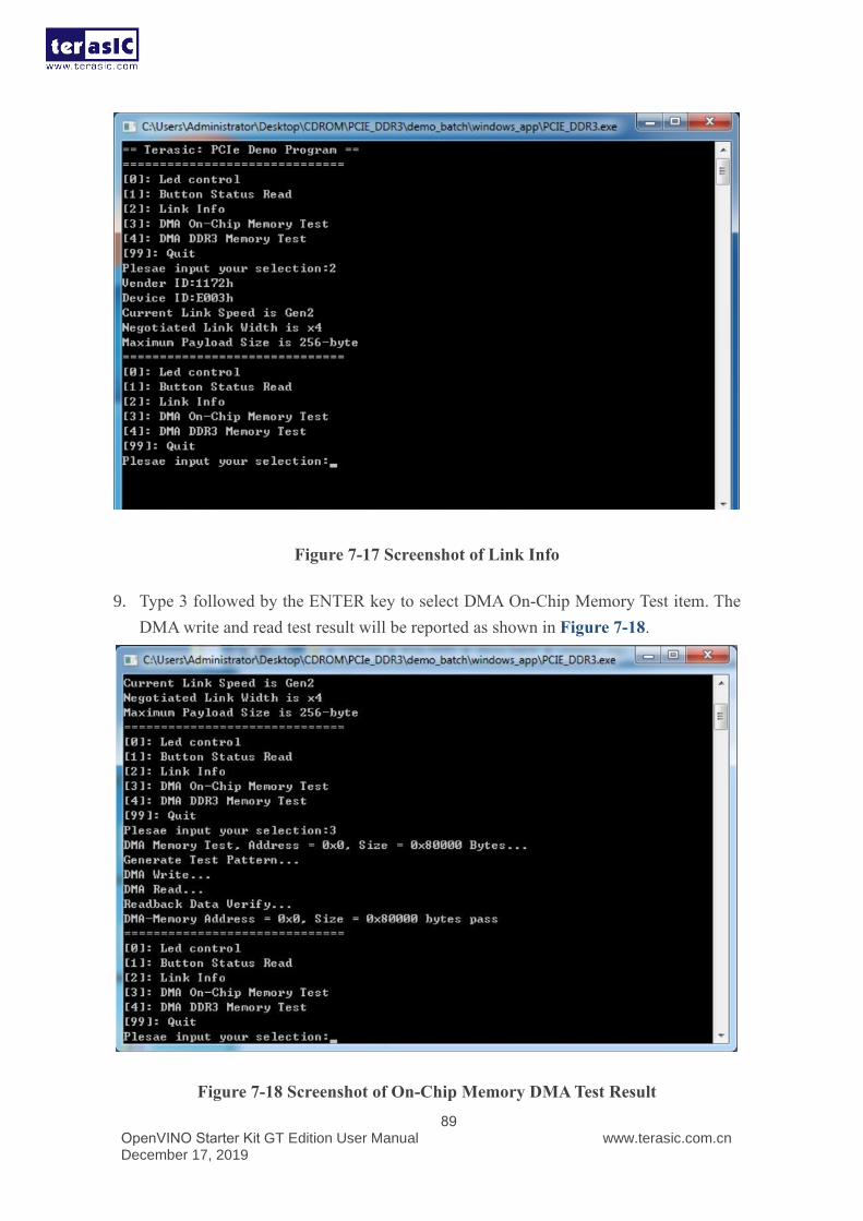
OpenVINO Starter Kit GT Edition User Manual December 17, 2019
www.terasic.com.cn
89
Figure 7-17 Screenshot of Link Info
9. Type 3 followed by the ENTER key to select DMA On-Chip Memory Test item. The
DMA write and read test result will be reported as shown in Figure 7-18.
Figure 7-18 Screenshot of On-Chip Memory DMA Test Result
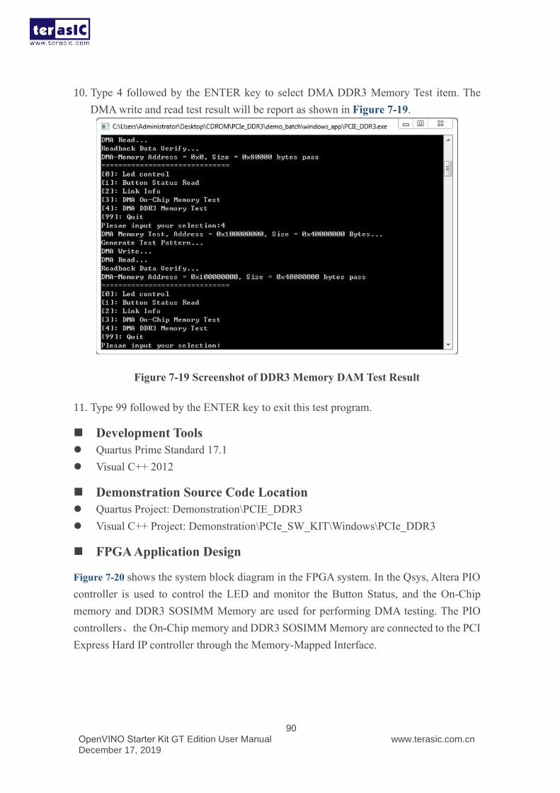
OpenVINO Starter Kit GT Edition User Manual December 17, 2019
www.terasic.com.cn
90
10. Type 4 followed by the ENTER key to select DMA DDR3 Memory Test item. The
DMA write and read test result will be report as shown in Figure 7-19.
Figure 7-19 Screenshot of DDR3 Memory DAM Test Result
11. Type 99 followed by the ENTER key to exit this test program.
◼ Development Tools
⚫ Quartus Prime Standard 17.1
⚫ Visual C++ 2012
◼ Demonstration Source Code Location
⚫ Quartus Project: Demonstration\PCIE_DDR3
⚫ Visual C++ Project: Demonstration\PCIe_SW_KIT\Windows\PCIe_DDR3
◼ FPGA Application Design
Figure 7-20 shows the system block diagram in the FPGA system. In the Qsys, Altera PIO
controller is used to control the LED and monitor the Button Status, and the On-Chip
memory and DDR3 SOSIMM Memory are used for performing DMA testing. The PIO
controllers、the On-Chip memory and DDR3 SOSIMM Memory are connected to the PCI
Express Hard IP controller through the Memory-Mapped Interface.
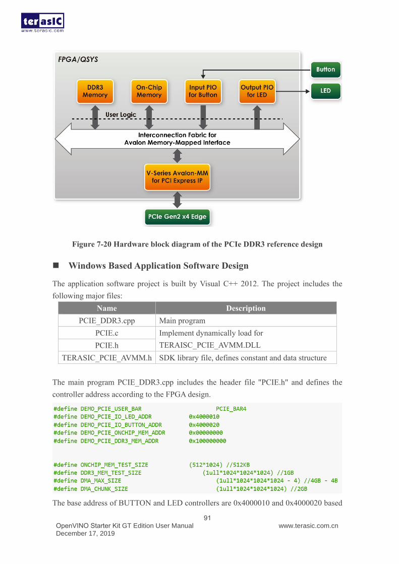
OpenVINO Starter Kit GT Edition User Manual December 17, 2019
www.terasic.com.cn
91
Figure 7-20 Hardware block diagram of the PCIe DDR3 reference design
◼ Windows Based Application Software Design
The application software project is built by Visual C++ 2012. The project includes the
following major files:
Name Description
PCIE_DDR3.cpp Main program
PCIE.c Implement dynamically load for
TERAISC_PCIE_AVMM.DLL PCIE.h
TERASIC_PCIE_AVMM.h SDK library file, defines constant and data structure
The main program PCIE_DDR3.cpp includes the header file "PCIE.h" and defines the
controller address according to the FPGA design.
The base address of BUTTON and LED controllers are 0x4000010 and 0x4000020 based
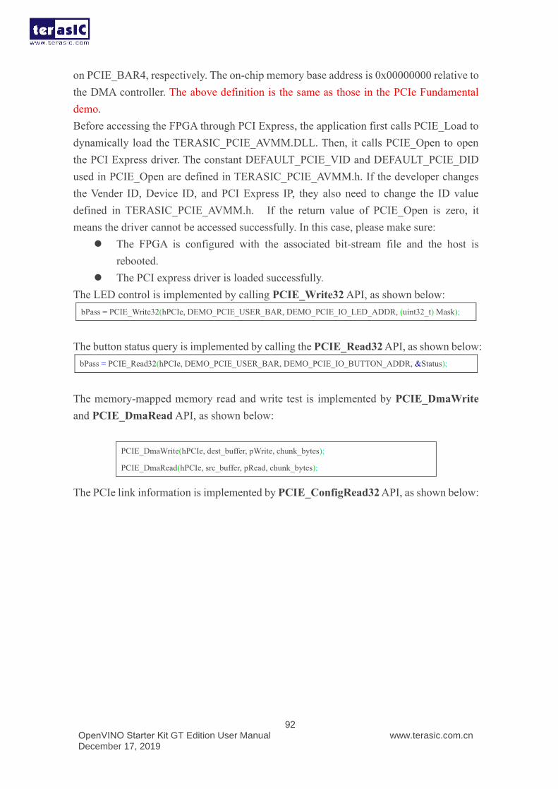
OpenVINO Starter Kit GT Edition User Manual December 17, 2019
www.terasic.com.cn
92
on PCIE_BAR4, respectively. The on-chip memory base address is 0x00000000 relative to
the DMA controller. The above definition is the same as those in the PCIe Fundamental
demo.
Before accessing the FPGA through PCI Express, the application first calls PCIE_Load to
dynamically load the TERASIC_PCIE_AVMM.DLL. Then, it calls PCIE_Open to open
the PCI Express driver. The constant DEFAULT_PCIE_VID and DEFAULT_PCIE_DID
used in PCIE_Open are defined in TERASIC_PCIE_AVMM.h. If the developer changes
the Vender ID, Device ID, and PCI Express IP, they also need to change the ID value
defined in TERASIC_PCIE_AVMM.h. If the return value of PCIE_Open is zero, it
means the driver cannot be accessed successfully. In this case, please make sure:
⚫ The FPGA is configured with the associated bit-stream file and the host is
rebooted.
⚫ The PCI express driver is loaded successfully.
The LED control is implemented by calling PCIE_Write32 API, as shown below:
bPass = PCIE_Write32(hPCIe, DEMO_PCIE_USER_BAR, DEMO_PCIE_IO_LED_ADDR, (uint32_t) Mask);
The button status query is implemented by calling the PCIE_Read32 API, as shown below:
bPass = PCIE_Read32(hPCIe, DEMO_PCIE_USER_BAR, DEMO_PCIE_IO_BUTTON_ADDR, &Status);
The memory-mapped memory read and write test is implemented by PCIE_DmaWrite
and PCIE_DmaRead API, as shown below:
The PCIe link information is implemented by PCIE_ConfigRead32 API, as shown below:
PCIE_DmaWrite(hPCIe, dest_buffer, pWrite, chunk_bytes);
PCIE_DmaRead(hPCIe, src_buffer, pRead, chunk_bytes);
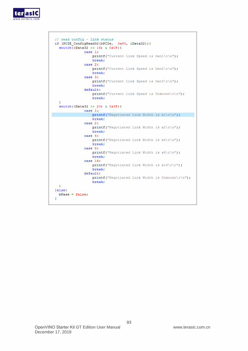
OpenVINO Starter Kit GT Edition User Manual December 17, 2019
www.terasic.com.cn
93
OpenVINO Starter Kit GT Edition User Manual December 17, 2019
www.terasic.com.cn
94
Chapter 8
PCIe Reference Design for Linux PCI Express is commonly used in consumer, server, and industrial applications, to link
motherboard-mounted peripherals. From this demonstration, it will show how the PC
Linux and FPGA communicate with each other through the PCI Express interface. V-Series
Avalon-MM DMA for PCI Express IP is used in this demonstration. For detail about this
IP, please refer to Intel document : V-Series Avalon-MM DMA Interface for PCIe Solutions
User Guide.
8.1 PCI Express System Infrastructure
Figure 8-1 shows the infrastructure of the PCI Express System in this demonstration. It
consists of two primary components: FPGA System and PC System. The FPGA System is
developed based on V-Series Avalon-MM DMA for PCI Express IP with Avalon-MM
DMA. The application software on the PC side is developed by Terasic based on Intel’s
PCIe kernel mode driver.
Figure 8-1 Infrastructure of PCI Express System
OpenVINO Starter Kit GT Edition User Manual December 17, 2019
www.terasic.com.cn
95
8.2 PCI Express Software SDK
The FPGA System CD contains a PC Windows based SDK to allow users to develop their
64-bit software application on 64-bits Linux. CentOS 7.2 is recommended. The SDK is
located in the “CD ROM/Demonstration/PCIe_SW_KIT/Linux” folder which includes:
⚫ PCI Express Driver
⚫ PCI Express Library
⚫ PCI Express Examples
The kernel mode driver assumes the PCIe vendor ID (VID) is 0x1172 and the device ID
(DID) is 0xE001. If different VID and DID are used in the design, users need to modify
the PCIe vendor ID (VID) and device ID (DID) in the driver project and rebuild the driver.
The ID is defined in the file: PCIe_SW_KIT/Linux/PCIe_Driver/altera_pcie_cmd.h.
The PCI Express Library is implemented as a single .so file named terasic_pcie_qsys.so.
This file is a 64-bit library file. With the library exported software API, users can easily
communicate with the FPGA. The library provides the following functions:
⚫ Basic data read and write
⚫ Data read and write by DMA
For high performance data transmission, Altera AVMM DMA is required as the read and
write operations are specified under the hardware design on the FPGA.
8.3 PCI Express Software Stack
Figure 8-2 shows the software stack for the PCI Express application software on 64-bit
Linux. The PCIe library module terasic_pcie_qys.so provides DMA and direct I/O access
for user application program to communicate with FPGA. Users can develop their
applications based on this .so library file. The altera_pcie.ko kernel driver is provided by
Altera.
OpenVINO Starter Kit GT Edition User Manual December 17, 2019
www.terasic.com.cn
96
Figure 8-2 PCI Express Software Stack
◼ Install PCI Express Driver on Linux
To make sure the PCIe driver can meet your kernel of Linux distribution, the driver
altera_pcie.ko should be recompile before use it. The PCIe driver project is locate in the
folder: CD ROM/Demonstrations/PCIe_SW_KIT/Linux/PCIe_Driver
The folder includes the following files:
⚫ altera_pcie.c
⚫ altera_pcie.h
⚫ altera_pcie_cmd.h
⚫ Makefile
⚫ load_driver
⚫ unload
⚫ config_file
To compile and install the PCI Express driver, please execute the steps below:
1. Install the OpenVINO Starter Kit on the PCIe slot of the host PC.
2. Make sure Quartus Programmer and USB-Blaster II driver are installed.
3. Power on your OpenVINO Starter Kit and the host PC.
4. Open a terminal and use "cd" command to goto the path "CDROM/Demonstration/
PCIe_Fundamental/demo_batch".
5. Set QUARTUS_ROOTDIR variable pointing to the Quartus installation path. Set
QUARTUS_ROOTDIR variable by tying the following commands in terminal.
Replace “/home/centos/intelFPGA/17.1/quartus” to your quartus installation path.
OpenVINO Starter Kit GT Edition User Manual December 17, 2019
www.terasic.com.cn
97
6. Execute "sudo sh test.sh" command to configure the FPGA
7. Restart Linux operation system. In Linux, open a terminal and use “cd” command to
goto the PCIe_Driver path.
8. Type the following commands to compile and install the driver altera_pcie.ko, and
make sure driver is loaded successfully and FPGA is detected by the driver as shown
in Figure 8-3.
make
sudo sh load_driver
dmesg | tail -n 15
Figure 8-3 Screenshot of install PCIe driver
◼ Create a Software Application
All the files needed to create a PCIe software application are located in the directory CD
ROM/Demonstration/PCIe_SW_KIT/Linux/PCIe_Library. It includes the following files:
⚫ TERASIC_PCIE_AVMM.h
⚫ terasic_pcie_qsys.so (64-bit library)
Below list the procedures to use the library in users’ C/C++ project:
1. Create a 64-bit C/C++ project.
2. Include TERASIC_PCIE_AVMM.h in the C/C++ project.
3. Copy terasic_pcie_qsys.so to the folder where project execution file is located.
4. Dynamically load terasic_pcie_qsys.so in C/C++ program. To load the
terasic_pcie_qsys.so, please refer to the PCIe fundamental example below.
export QUARTUS_ROOTDIR=/home/centos/intelFPGA/17.1/quartus
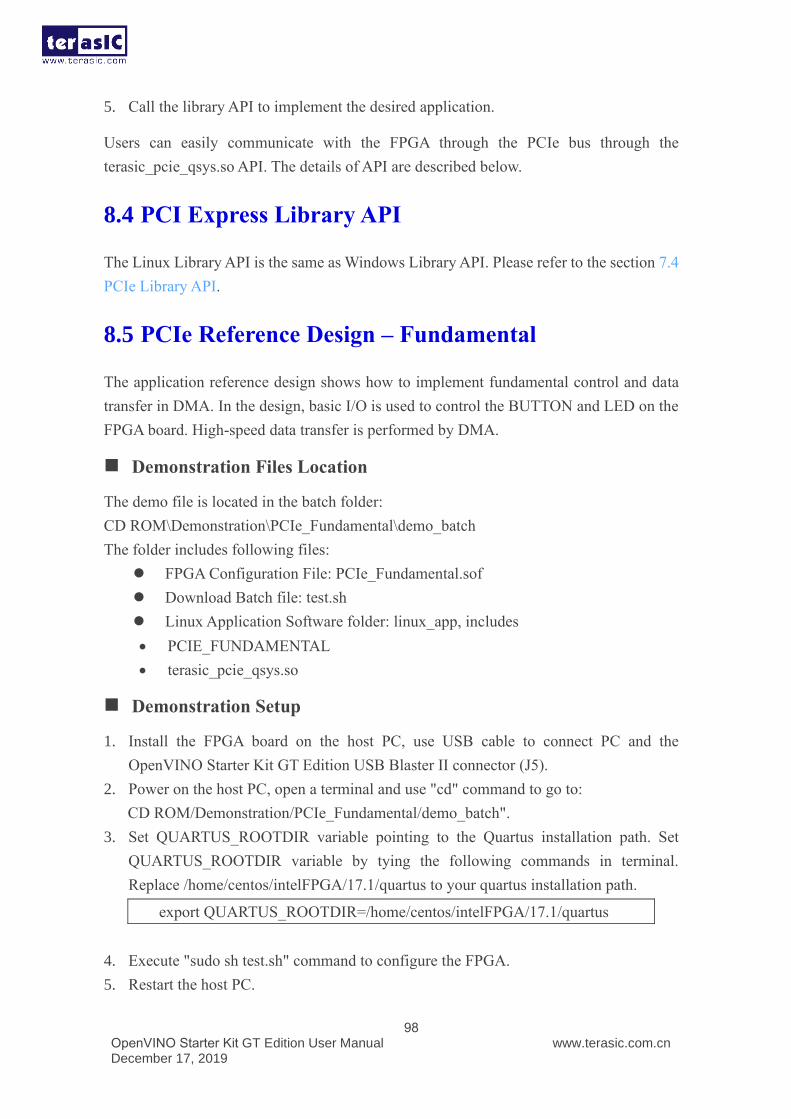
OpenVINO Starter Kit GT Edition User Manual December 17, 2019
www.terasic.com.cn
98
5. Call the library API to implement the desired application.
Users can easily communicate with the FPGA through the PCIe bus through the
terasic_pcie_qsys.so API. The details of API are described below.
8.4 PCI Express Library API
The Linux Library API is the same as Windows Library API. Please refer to the section 7.4
PCIe Library API.
8.5 PCIe Reference Design – Fundamental
The application reference design shows how to implement fundamental control and data
transfer in DMA. In the design, basic I/O is used to control the BUTTON and LED on the
FPGA board. High-speed data transfer is performed by DMA.
◼ Demonstration Files Location
The demo file is located in the batch folder:
CD ROM\Demonstration\PCIe_Fundamental\demo_batch
The folder includes following files:
⚫ FPGA Configuration File: PCIe_Fundamental.sof
⚫ Download Batch file: test.sh
⚫ Linux Application Software folder: linux_app, includes
• PCIE_FUNDAMENTAL
• terasic_pcie_qsys.so
◼ Demonstration Setup
1. Install the FPGA board on the host PC, use USB cable to connect PC and the
OpenVINO Starter Kit GT Edition USB Blaster II connector (J5).
2. Power on the host PC, open a terminal and use "cd" command to go to:
CD ROM/Demonstration/PCIe_Fundamental/demo_batch".
3. Set QUARTUS_ROOTDIR variable pointing to the Quartus installation path. Set
QUARTUS_ROOTDIR variable by tying the following commands in terminal.
Replace /home/centos/intelFPGA/17.1/quartus to your quartus installation path.
4. Execute "sudo sh test.sh" command to configure the FPGA.
5. Restart the host PC.
export QUARTUS_ROOTDIR=/home/centos/intelFPGA/17.1/quartus
OpenVINO Starter Kit GT Edition User Manual December 17, 2019
www.terasic.com.cn
99
6. Install PCIe driver. The driver is located in the folder:
CD ROM/Demonstration/PCIe_SW_KIT/Linux/PCIe_Driver.
7. Type “ls –l /dev/altera_pcie*” to make sure the Linux has detected the FPGA Board. If
the FPGA board is detected, developers can find the /dev/altera_pcieX(where X is
0~255) in Linux file system as shown in Figure 8-4.
Figure 8-4 Linux has detected the FPGA Board
8. Go to linux_app folder, execute PCIE_FUNDAMENTAL. A menu will appear as
shown in Figure 8-5.
Figure 8-5 Screenshot of Program Menu
9. Type 0 followed by a ENTER key to select Led Control item, then input 3 (hex 0x03)
will make LEDG0 and LEDG1 on as shown in Figure 8-6. If input 0 (hex 0x00), all
Led will be turn off.
OpenVINO Starter Kit GT Edition User Manual December 17, 2019
www.terasic.com.cn
100
Figure 8-6 Screenshot of LED Control
10. Type 1 followed by an ENTER key to select Button Status Read item. The button status
will be report as shown in Figure 8-7.
Figure 8-7 Screenshot of Button Status Report
11. Type 2 followed by an ENTER key to select DMA Testing item. The DMA test result
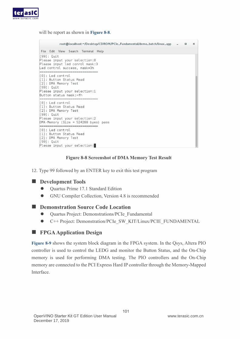
OpenVINO Starter Kit GT Edition User Manual December 17, 2019
www.terasic.com.cn
101
will be report as shown in Figure 8-8.
Figure 8-8 Screenshot of DMA Memory Test Result
12. Type 99 followed by an ENTER key to exit this test program
◼ Development Tools
⚫ Quartus Prime 17.1 Standard Edition
⚫ GNU Compiler Collection, Version 4.8 is recommended
◼ Demonstration Source Code Location
⚫ Quartus Project: Demonstrations/PCIe_Fundamental
⚫ C++ Project: Demonstration/PCIe_SW_KIT/Linux/PCIE_FUNDAMENTAL
◼ FPGA Application Design
Figure 8-9 shows the system block diagram in the FPGA system. In the Qsys, Altera PIO
controller is used to control the LEDG and monitor the Button Status, and the On-Chip
memory is used for performing DMA testing. The PIO controllers and the On-Chip
memory are connected to the PCI Express Hard IP controller through the Memory-Mapped
Interface.
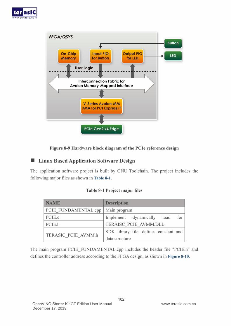
OpenVINO Starter Kit GT Edition User Manual December 17, 2019
www.terasic.com.cn
102
Figure 8-9 Hardware block diagram of the PCIe reference design
◼ Linux Based Application Software Design
The application software project is built by GNU Toolchain. The project includes the
following major files as shown in Table 8-1.
Table 8-1 Project major files
NAME Description
PCIE_FUNDAMENTAL.cpp Main program
PCIE.c Implement dynamically load for
TERAISC_PCIE_AVMM.DLL PCIE.h
TERASIC_PCIE_AVMM.h SDK library file, defines constant and
data structure
The main program PCIE_FUNDAMENTAL.cpp includes the header file "PCIE.h" and
defines the controller address according to the FPGA design, as shown in Figure 8-10.
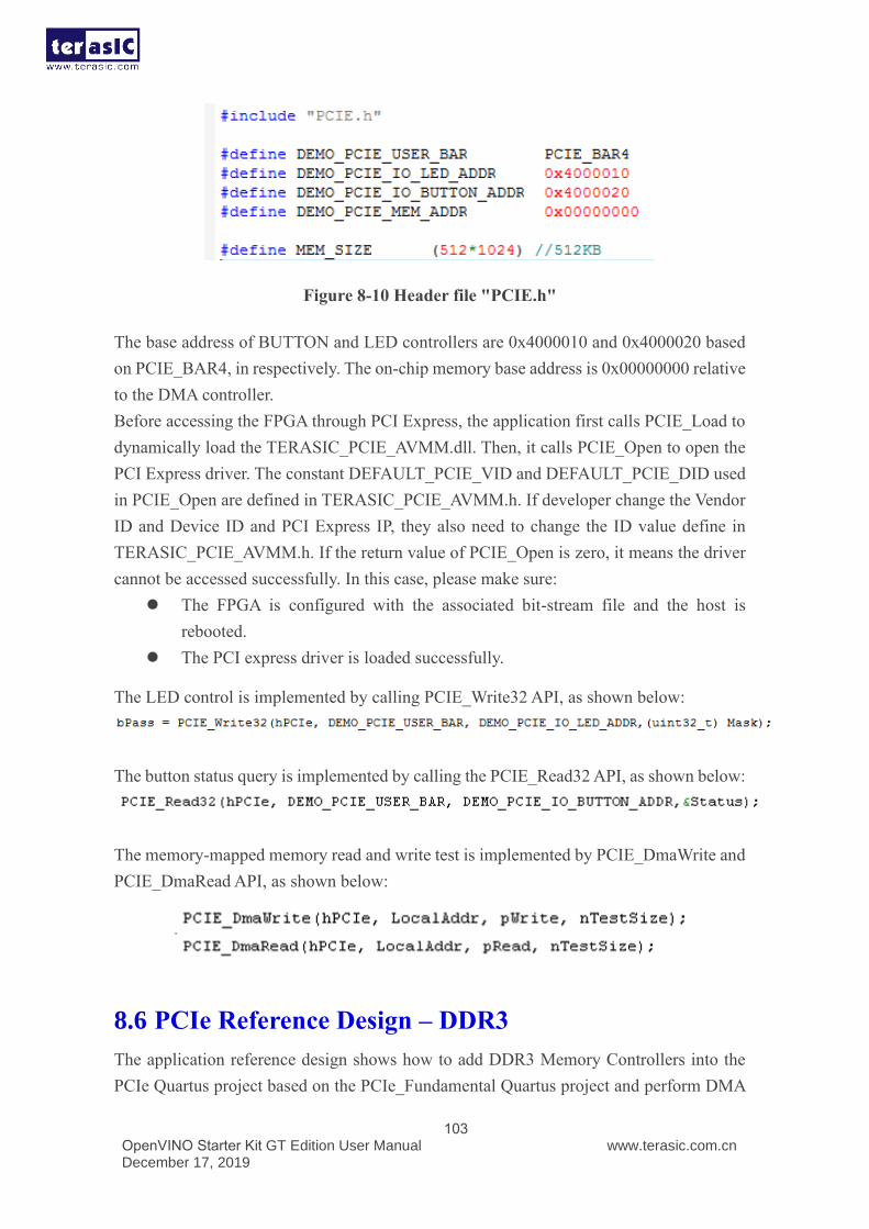
OpenVINO Starter Kit GT Edition User Manual December 17, 2019
www.terasic.com.cn
103
Figure 8-10 Header file "PCIE.h"
The base address of BUTTON and LED controllers are 0x4000010 and 0x4000020 based
on PCIE_BAR4, in respectively. The on-chip memory base address is 0x00000000 relative
to the DMA controller.
Before accessing the FPGA through PCI Express, the application first calls PCIE_Load to
dynamically load the TERASIC_PCIE_AVMM.dll. Then, it calls PCIE_Open to open the
PCI Express driver. The constant DEFAULT_PCIE_VID and DEFAULT_PCIE_DID used
in PCIE_Open are defined in TERASIC_PCIE_AVMM.h. If developer change the Vendor
ID and Device ID and PCI Express IP, they also need to change the ID value define in
TERASIC_PCIE_AVMM.h. If the return value of PCIE_Open is zero, it means the driver
cannot be accessed successfully. In this case, please make sure:
⚫ The FPGA is configured with the associated bit-stream file and the host is
rebooted.
⚫ The PCI express driver is loaded successfully.
The LED control is implemented by calling PCIE_Write32 API, as shown below:
The button status query is implemented by calling the PCIE_Read32 API, as shown below:
The memory-mapped memory read and write test is implemented by PCIE_DmaWrite and
PCIE_DmaRead API, as shown below:
8.6 PCIe Reference Design – DDR3
The application reference design shows how to add DDR3 Memory Controllers into the
PCIe Quartus project based on the PCIe_Fundamental Quartus project and perform DMA
OpenVINO Starter Kit GT Edition User Manual December 17, 2019
www.terasic.com.cn
104
data transmission. Also, this demo shows how to call “PCIE_ConfigRead32” API to check
PCIe link status.
◼ Demonstration Files Location
The demo file is located in the batch folder:
CD ROM\ Demonstrations\PCIE_DDR3\demo_batch
The folder includes following files:
• FPGA Configuration File: PCIE_DDR3.sof
• Download Batch file: test.sh
• Linux Application Software folder: linux_app, includes
• PCIE_DDR3
• terasic_pcie_qsys.so
◼ Demonstration Setup
1. Install the FPGA board on the host PC, install the FPGA board on the host PC, use USB
cable to connect PC and the OpenVINO Starter Kit GT Edition USB Blaster II
connector (J5).
2. Power on the host PC, open a terminal and use "cd" command to go to
"CD ROM/Demonstration/PCIe_Fundamental/demo_batch".
3. Set QUARTUS_ROOTDIR variable pointing to the Quartus installation path. Set
QUARTUS_ROOTDIR variable by tying the following commands in terminal.
Replace /home/centos/intelFPGA/17.1/quartus to your quartus installation path.
4. Execute "sudo sh test.sh" command to configure the FPGA
5. Restart the host PC.
6. Install PCIe driver (If it is necessary). The driver is located in the folder:
CD ROM/Demonstration/PCIe_SW_KIT/Linux/PCIe_Driver.
7. Make sure the Linux host PC has detected the FPGA Board.
8. Go to linux_app folder, execute PCIE_DDR3. A menu will appear as shown in Figure
8-11.
export QUARTUS_ROOTDIR=/home/centos/intelFPGA/17.1/quartus
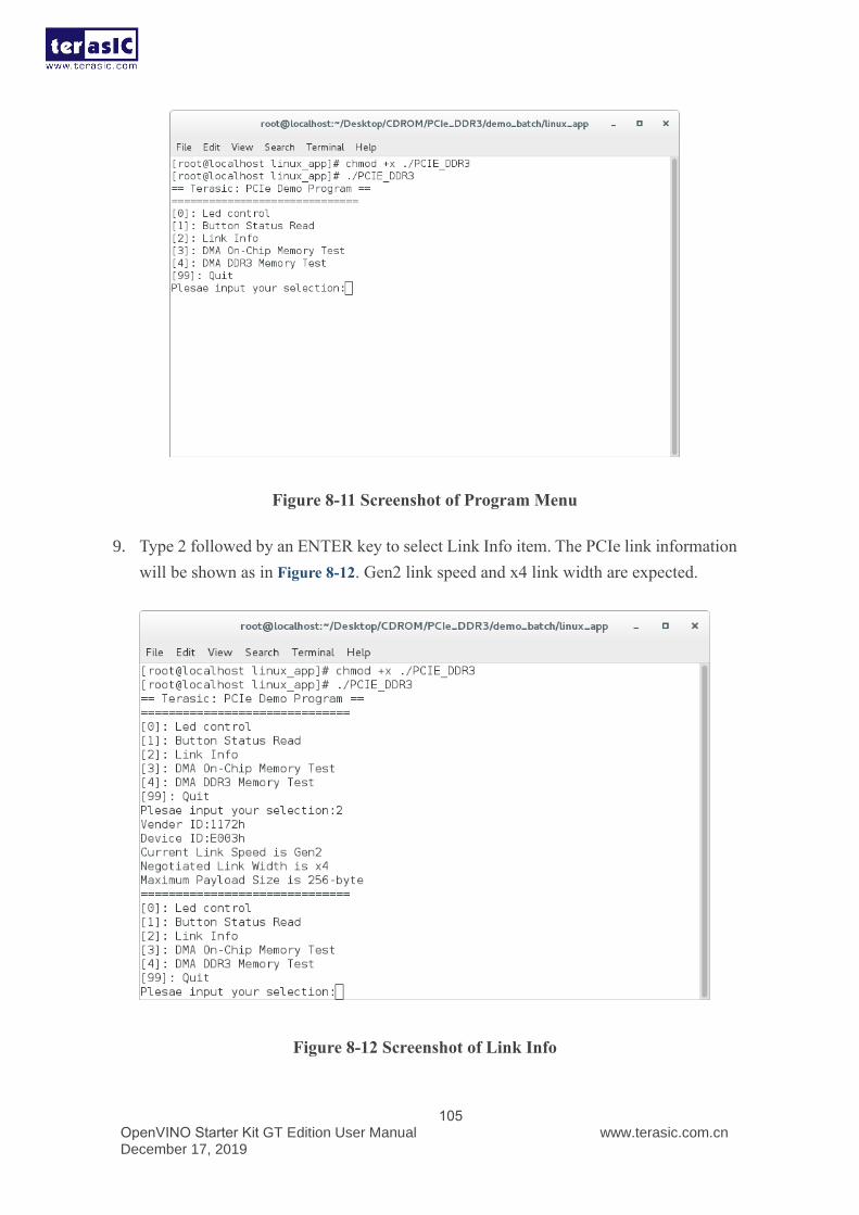
OpenVINO Starter Kit GT Edition User Manual December 17, 2019
www.terasic.com.cn
105
Figure 8-11 Screenshot of Program Menu
9. Type 2 followed by an ENTER key to select Link Info item. The PCIe link information
will be shown as in Figure 8-12. Gen2 link speed and x4 link width are expected.
Figure 8-12 Screenshot of Link Info
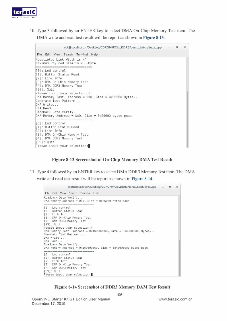
OpenVINO Starter Kit GT Edition User Manual December 17, 2019
www.terasic.com.cn
106
10. Type 3 followed by an ENTER key to select DMA On-Chip Memory Test item. The
DMA write and read test result will be report as shown in Figure 8-13.
Figure 8-13 Screenshot of On-Chip Memory DMA Test Result
11. Type 4 followed by an ENTER key to select DMA DDR3 Memory Test item. The DMA
write and read test result will be report as shown in Figure 8-14.
Figure 8-14 Screenshot of DDR3 Memory DAM Test Result
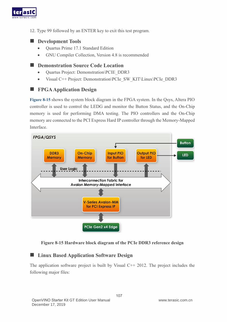
OpenVINO Starter Kit GT Edition User Manual December 17, 2019
www.terasic.com.cn
107
12. Type 99 followed by an ENTER key to exit this test program.
◼ Development Tools
• Quartus Prime 17.1 Standard Edition
• GNU Compiler Collection, Version 4.8 is recommended
◼ Demonstration Source Code Location
• Quartus Project: Demonstration\PCIE_DDR3
• Visual C++ Project: Demonstration\PCIe_SW_KIT\Linux\PCIe_DDR3
◼ FPGA Application Design
Figure 8-15 shows the system block diagram in the FPGA system. In the Qsys, Altera PIO
controller is used to control the LEDG and monitor the Button Status, and the On-Chip
memory is used for performing DMA testing. The PIO controllers and the On-Chip
memory are connected to the PCI Express Hard IP controller through the Memory-Mapped
Interface.
Figure 8-15 Hardware block diagram of the PCIe DDR3 reference design
◼ Linux Based Application Software Design
The application software project is built by Visual C++ 2012. The project includes the
following major files:
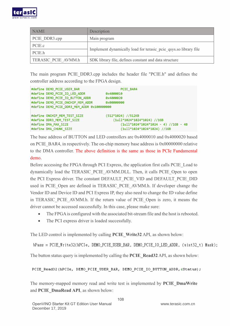
OpenVINO Starter Kit GT Edition User Manual December 17, 2019
www.terasic.com.cn
108
NAME Description
PCIE_DDR3.cpp Main program
PCIE.c Implement dynamically load for terasic_pcie_qsys.so library file
PCIE.h
TERASIC_PCIE_AVMM.h SDK library file, defines constant and data structure
The main program PCIE_DDR3.cpp includes the header file "PCIE.h" and defines the
controller address according to the FPGA design.
The base address of BUTTON and LED controllers are 0x4000010 and 0x4000020 based
on PCIE_BAR4, in respectively. The on-chip memory base address is 0x00000000 relative
to the DMA controller. The above definition is the same as those in PCIe Fundamental
demo.
Before accessing the FPGA through PCI Express, the application first calls PCIE_Load to
dynamically load the TERASIC_PCIE_AVMM.DLL. Then, it calls PCIE_Open to open
the PCI Express driver. The constant DEFAULT_PCIE_VID and DEFAULT_PCIE_DID
used in PCIE_Open are defined in TERASIC_PCIE_AVMM.h. If developer change the
Vendor ID and Device ID and PCI Express IP, they also need to change the ID value define
in TERASIC_PCIE_AVMM.h. If the return value of PCIE_Open is zero, it means the
driver cannot be accessed successfully. In this case, please make sure:
• The FPGA is configured with the associated bit-stream file and the host is rebooted.
• The PCI express driver is loaded successfully.
The LED control is implemented by calling PCIE_Write32 API, as shown below:
The button status query is implemented by calling the PCIE_Read32 API, as shown below:
The memory-mapped memory read and write test is implemented by PCIE_DmaWrite
and PCIE_DmaRead API, as shown below:
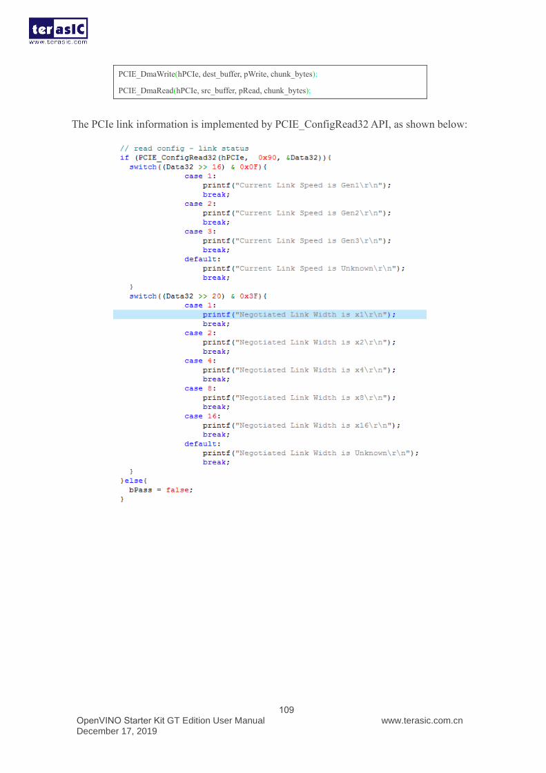
OpenVINO Starter Kit GT Edition User Manual December 17, 2019
www.terasic.com.cn
109
PCIE_DmaWrite(hPCIe, dest_buffer, pWrite, chunk_bytes);
PCIE_DmaRead(hPCIe, src_buffer, pRead, chunk_bytes);
The PCIe link information is implemented by PCIE_ConfigRead32 API, as shown below:

OpenVINO Starter Kit GT Edition User Manual December 17, 2019
www.terasic.com.cn
110
Chapter 9
Appendix
9.1 Revision History
Version Changes Log
V1.0 Initial version
V1.1 Change cover image and Figure 2-1
9.2 Copyright Statement
Copyright© Terasic Technologies Inc. All Rights Reserved.
Mouser Electronics
Authorized Distributor
Click to View Pricing, Inventory, Delivery & Lifecycle Information: Terasic:
P0559 P0559-EDU