Embed Size (px)
Citation preview
1
Microelectronics Processing Course - J. Salzman – Fall 2006
Microelectronics Processing Ion Implantation
2
Microelectronics Processing Course - J. Salzman – Fall 2006
Issues in Ion Implantation
•Equipment
•Dose, Range, Straggle
• Implantation Profile
•Junction Depth
•Channeling
•Energy Loss Mechanisms
•Damage - Anneal
3
Microelectronics Processing Course - J. Salzman – Fall 2006
Ion Implantation
A process in which energetic, charged atoms or molecules are directly introduced into a substrate.
Acceleration energies range between 10-200 KeV. (Today also up to several MeV)
Primarily used to add dopant ions into the surface of silicon wafers.
Goal : to introduce a desired atomic species, with a specified quantity (dose), into the required depth, with lateral selectivity.
4
Microelectronics Processing Course - J. Salzman – Fall 2006
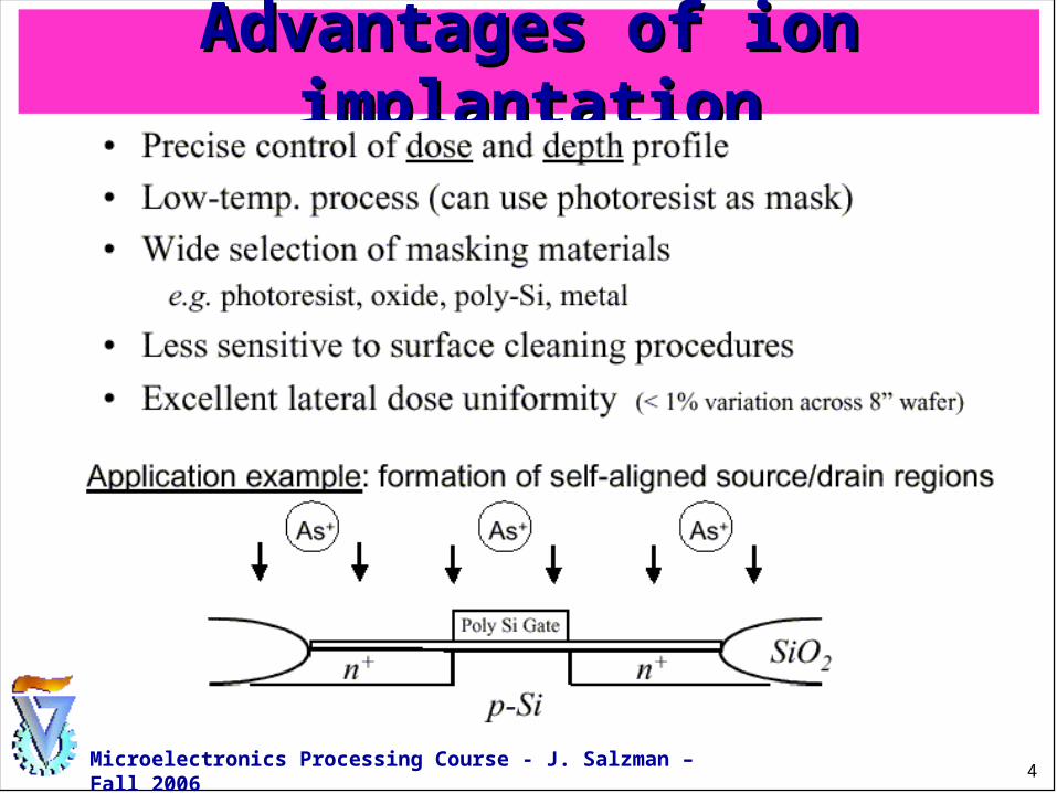
Advantages of ion implantationAdvantages of ion implantation
5
Microelectronics Processing Course - J. Salzman – Fall 2006
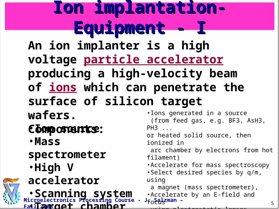
Ion implantation- Equipment - IIon implantation- Equipment - I
An ion implanter is a high voltage particle accelerator producing a high-velocity beam of ions which can penetrate the surface of silicon target wafers. Components: •Ion source•Mass spectrometer•High V accelerator•Scanning system•Target chamber
•Ions generated in a source (from feed gas, e.g. BF3, AsH3, PH3 ...or heated solid source, then ionized in arc chamber by electrons from hot filament)•Accelerate for mass spectroscopy•Select desired species by q/m, using a magnet (mass spectrometer),•Accelerate by an E-field and focus using electrostatic lensesimpact substrate in raster pattern.

6
Microelectronics Processing Course - J. Salzman – Fall 2006
7
Microelectronics Processing Course - J. Salzman – Fall 2006
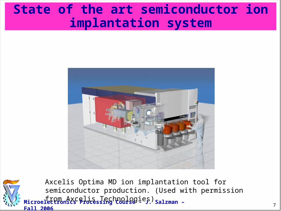
State of the art semiconductor ion implantation system
Axcelis Optima MD ion implantation tool for semiconductor production. (Used with permission from Axcelis Technologies)
8
Microelectronics Processing Course - J. Salzman – Fall 2006
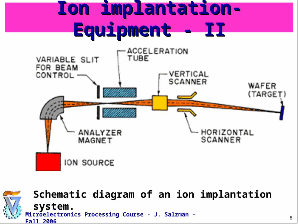
Ion implantation- Equipment - IIIon implantation- Equipment - II
Schematic diagram of an ion implantation system.
9
Microelectronics Processing Course - J. Salzman – Fall 2006
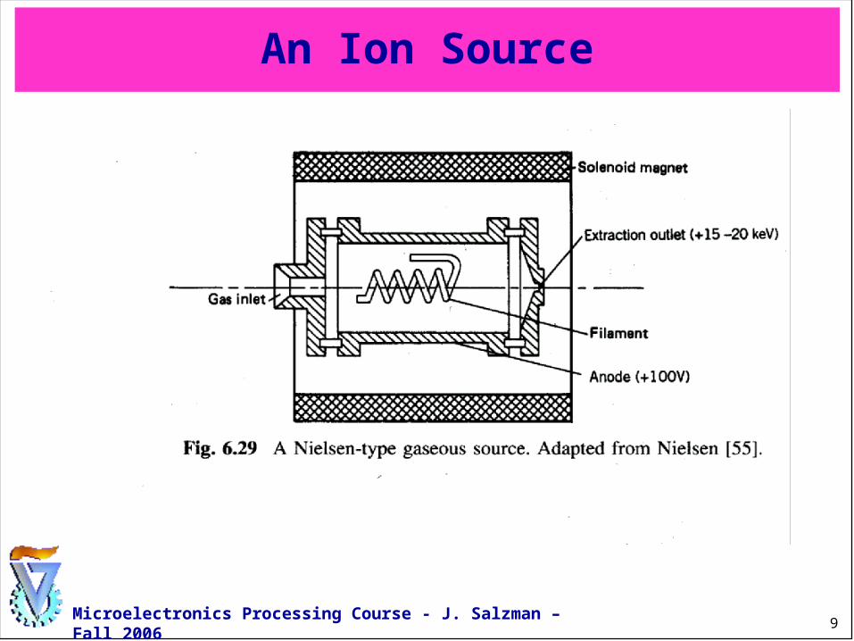
An Ion Source
10
Microelectronics Processing Course - J. Salzman – Fall 2006
Ion Implantation: A random Process
Each ion follows a random trajectory, scattering off silicon atoms, losing energyand coming to rest.
Since a large number of ions is implanted,the average range Rp and their straggle Rp
can be precisely predicted

11
Microelectronics Processing Course - J. Salzman – Fall 2006
Ion implantation-Range and StraggleIon implantation-Range and Straggle
Schematic diagram to show the range, the projected range RP , the
projected (ΔRP ) and lateral ΔR┴ straggle in ion implantation.
y
12
Microelectronics Processing Course - J. Salzman – Fall 2006
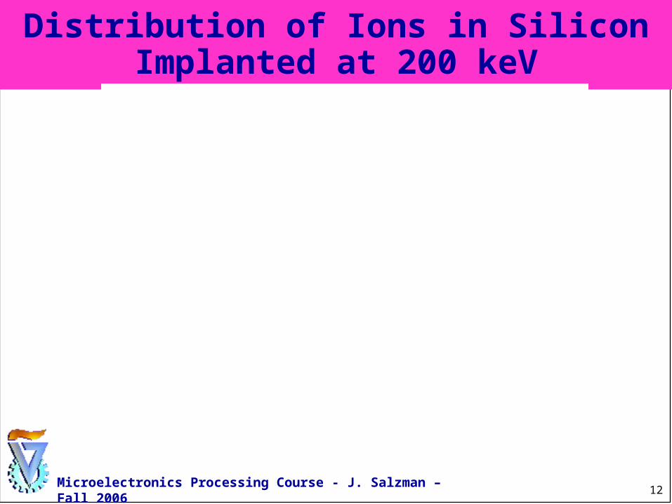
Distribution of Ions in SiliconImplanted at 200 keV
13
Microelectronics Processing Course - J. Salzman – Fall 2006
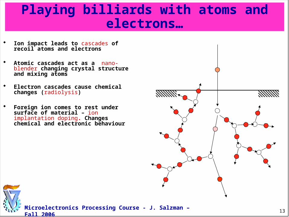
Playing billiards with atoms and electrons…
Ion impact leads to cascades of recoil atoms and electrons
Atomic cascades act as a nano-blender changing crystal structure and mixing atoms
Electron cascades cause chemical changes (radiolysis)
Foreign ion comes to rest under surface of material – ion implantation doping. Changes chemical and electronic behaviour
14
Microelectronics Processing Course - J. Salzman – Fall 2006
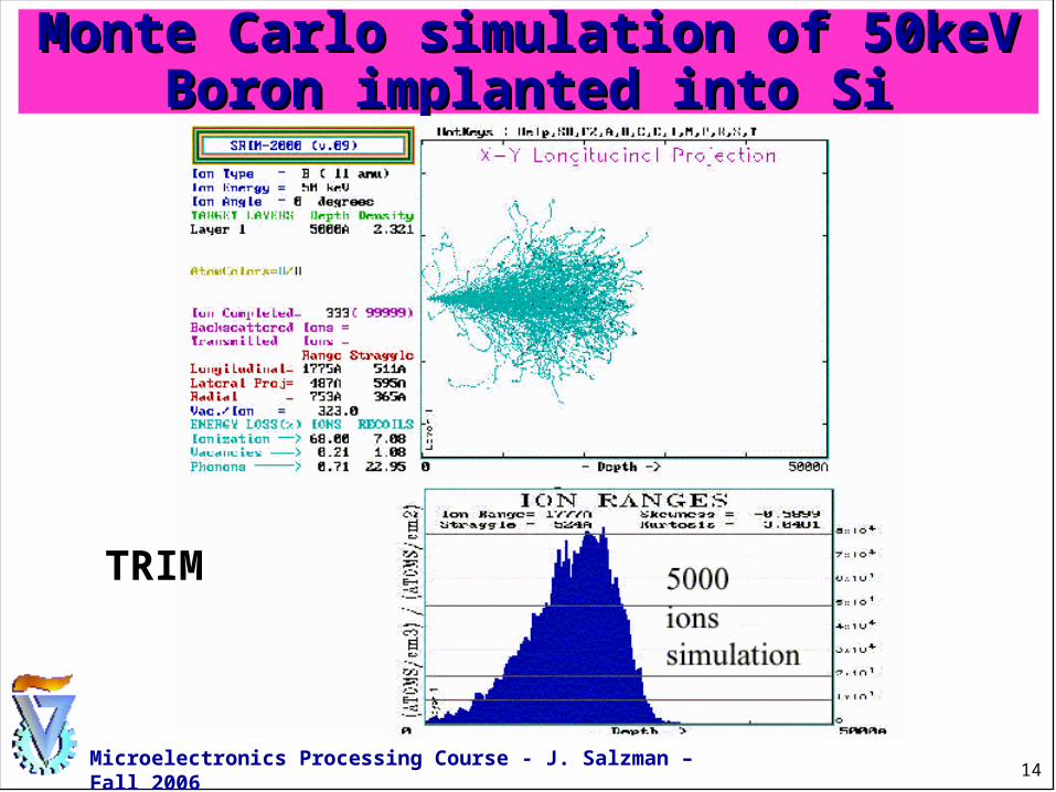
Monte Carlo simulation of 50keV Boron Monte Carlo simulation of 50keV Boron implanted into Siimplanted into Si
TRIM
15
Microelectronics Processing Course - J. Salzman – Fall 2006
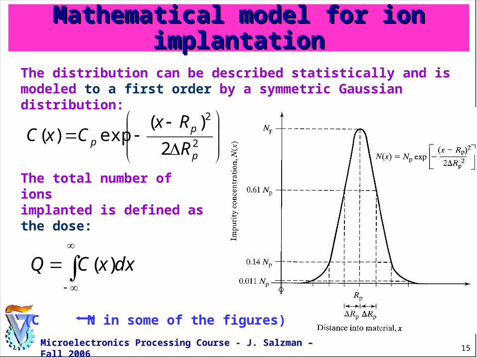
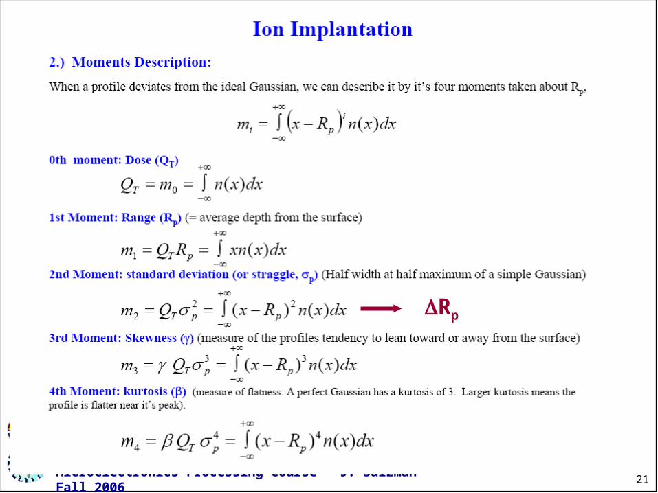
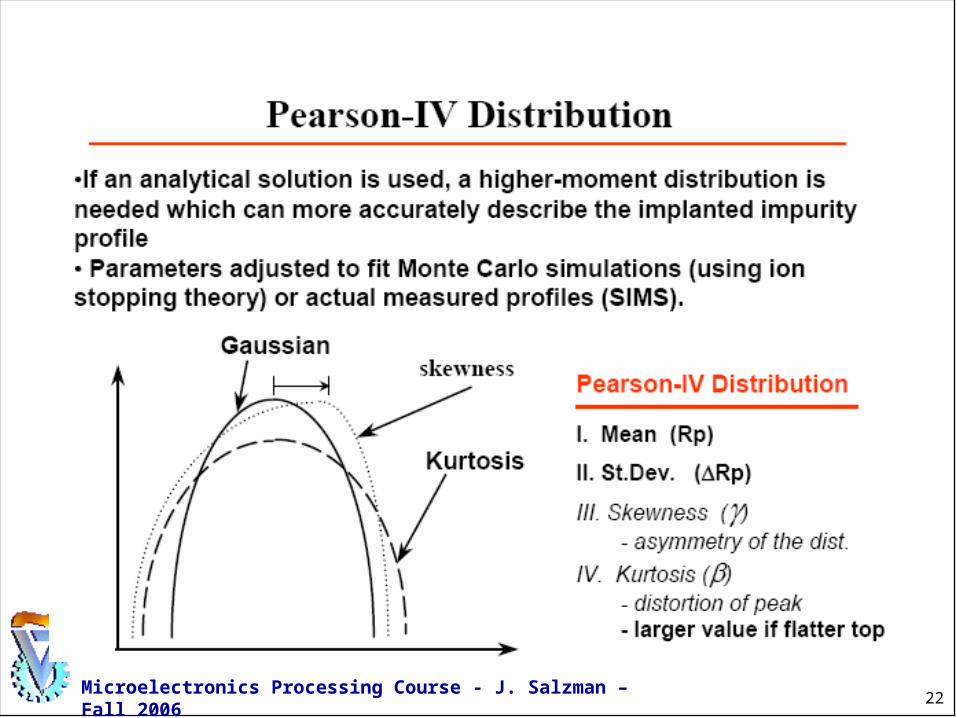
Mathematical model for ion Mathematical model for ion implantationimplantation
The distribution can be described statistically and is modeled to a first order by a symmetric Gaussian distribution:
2
2
2
)(exp)(
p
pp R
RxCxC
The total number of ionsimplanted is defined as the dose:
dxxCQ )(
(C N in some of the figures)
16
Microelectronics Processing Course - J. Salzman – Fall 2006
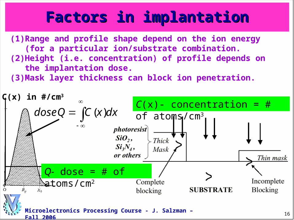
Factors in implantationFactors in implantation (1) Range and profile shape depend on the ion energy (for a particular
ion/substrate combination.(2) Height (i.e. concentration) of profile depends on the implantation
dose.(3) Mask layer thickness can block ion penetration.
C(x) in #/cm3
dxxCQdose )(C(x)- concentration = # of atoms/cm3
Q- dose = # of atoms/cm2
17
Microelectronics Processing Course - J. Salzman – Fall 2006
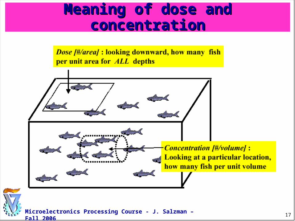
Meaning of dose and Meaning of dose and concentrationconcentration
18
Microelectronics Processing Course - J. Salzman – Fall 2006
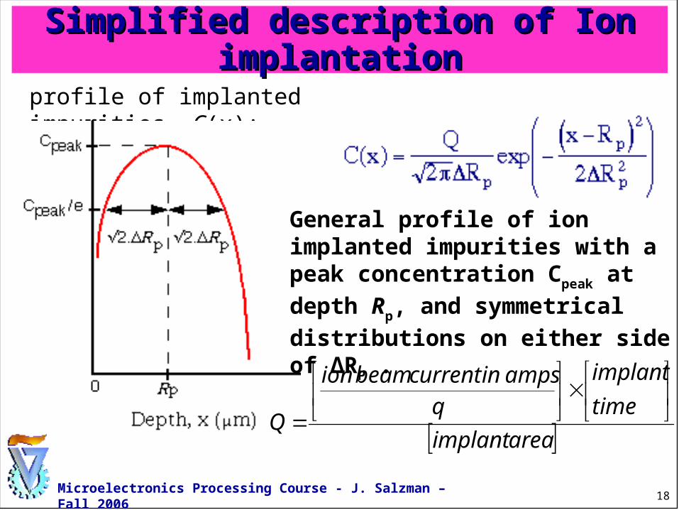
Simplified description of Ion Simplified description of Ion implantationimplantation
profile of implanted impurities, C(x):
General profile of ion implanted impurities with a peak concentration Cpeak at depth Rp, and
symmetrical distributions on either side of ΔRP .
areaimplant
time
implant
qampsincurrentbeamion
Q
19
Microelectronics Processing Course - J. Salzman – Fall 2006
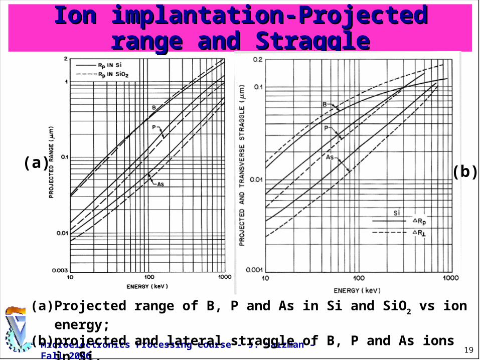
Ion implantation-Projected range Ion implantation-Projected range and Straggleand Straggle
(a) Projected range of B, P and As in Si and SiO2 vs ion energy;
(b) projected and lateral straggle of B, P and As ions in Si.
(a) (b)
20
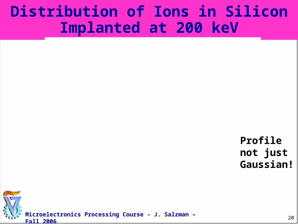
Microelectronics Processing Course - J. Salzman – Fall 2006
Distribution of Ions in SiliconImplanted at 200 keV
Profilenot just Gaussian!
21
Microelectronics Processing Course - J. Salzman – Fall 2006
Rp
22
Microelectronics Processing Course - J. Salzman – Fall 2006
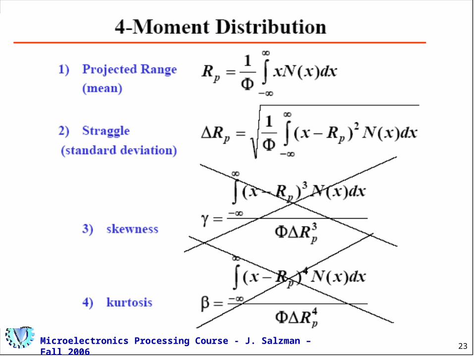
23
Microelectronics Processing Course - J. Salzman – Fall 2006
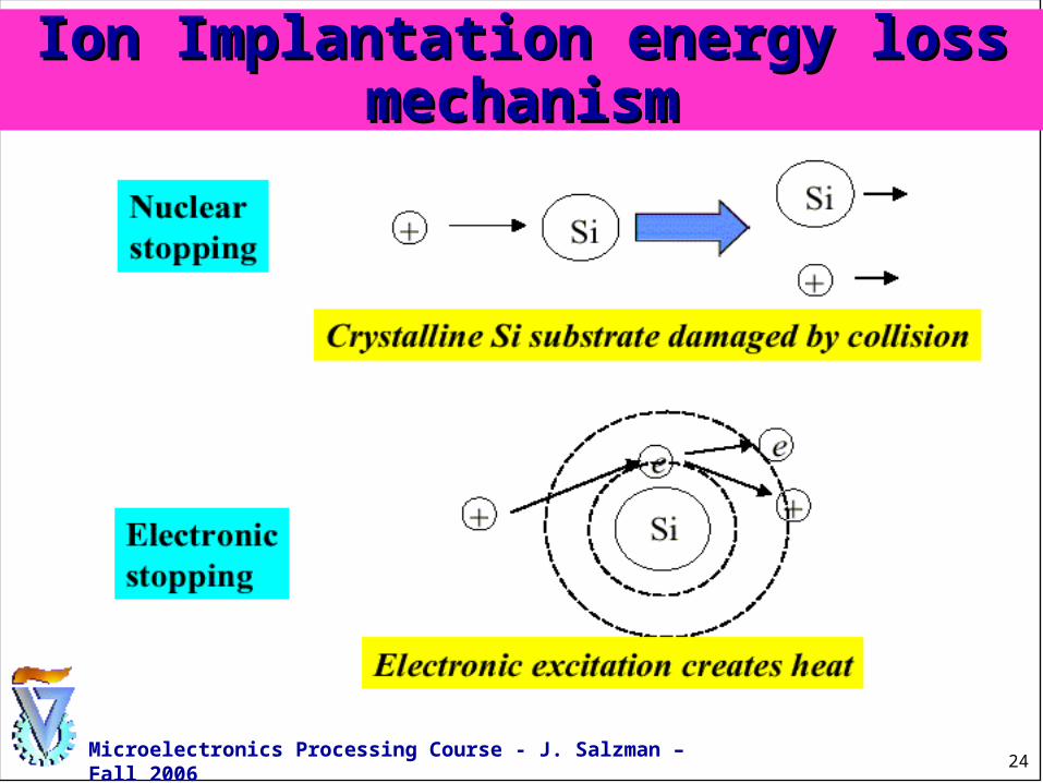
24
Microelectronics Processing Course - J. Salzman – Fall 2006
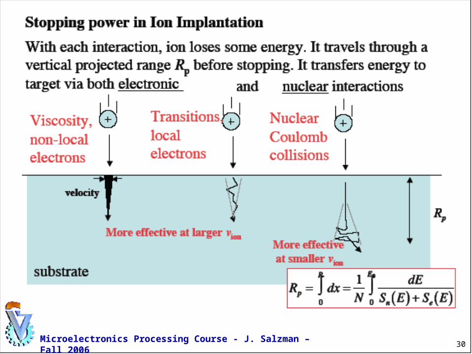
Ion Implantation energy loss Ion Implantation energy loss mechanismmechanism
25
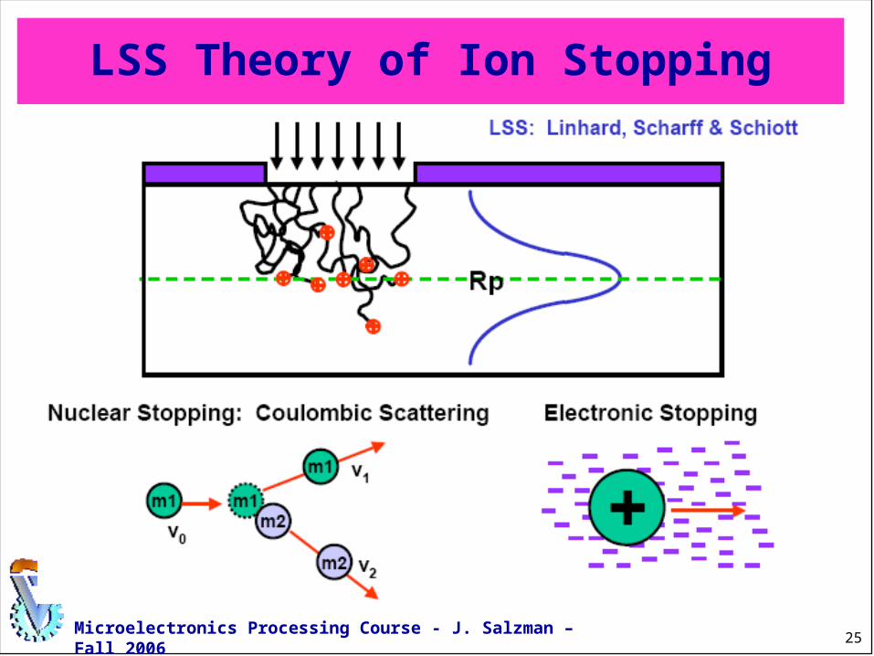
Microelectronics Processing Course - J. Salzman – Fall 2006
LSS Theory of Ion Stopping
26
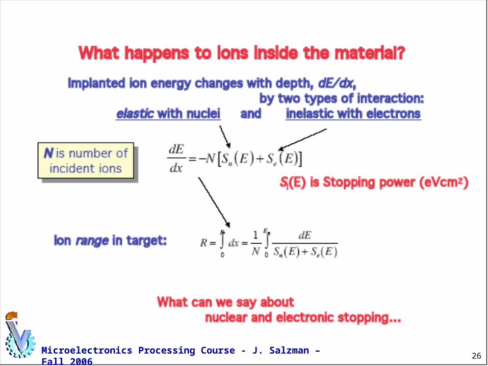
Microelectronics Processing Course - J. Salzman – Fall 2006
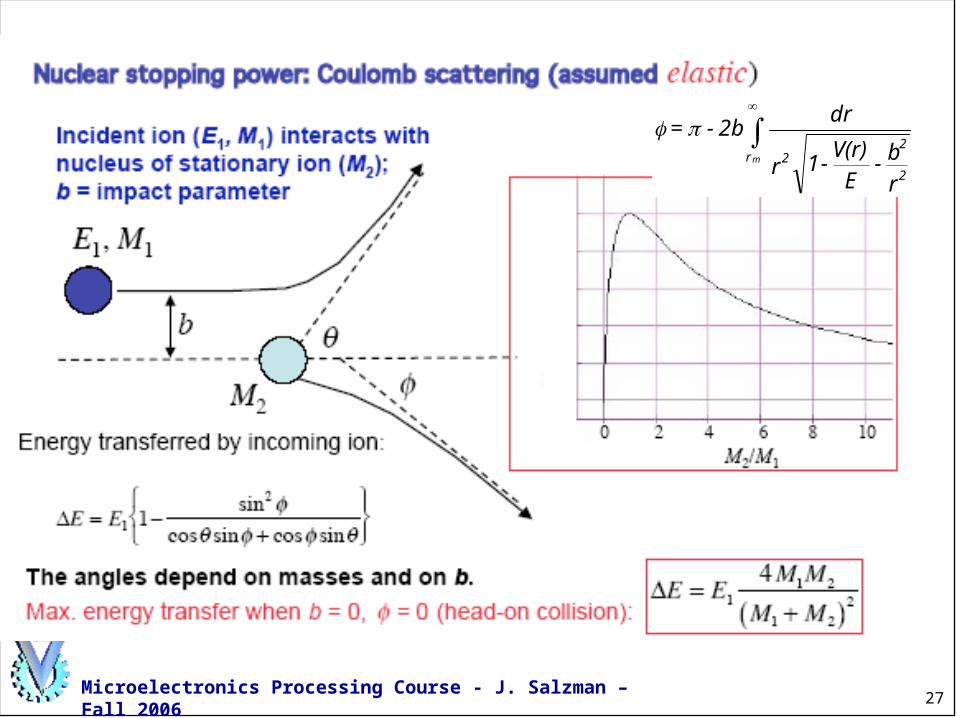
27
Microelectronics Processing Course - J. Salzman – Fall 2006
r
b - E
V(r) - 1 r
dr 2b - =
2
22r m
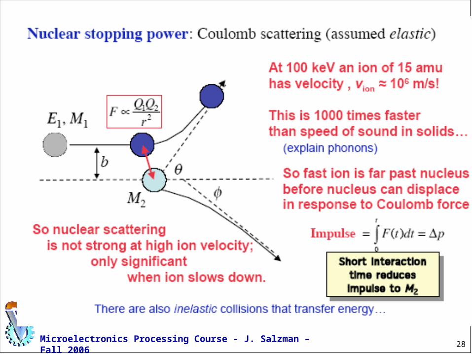
28
Microelectronics Processing Course - J. Salzman – Fall 2006
29
Microelectronics Processing Course - J. Salzman – Fall 2006
30
Microelectronics Processing Course - J. Salzman – Fall 2006
31
Microelectronics Processing Course - J. Salzman – Fall 2006
32
Microelectronics Processing Course - J. Salzman – Fall 2006
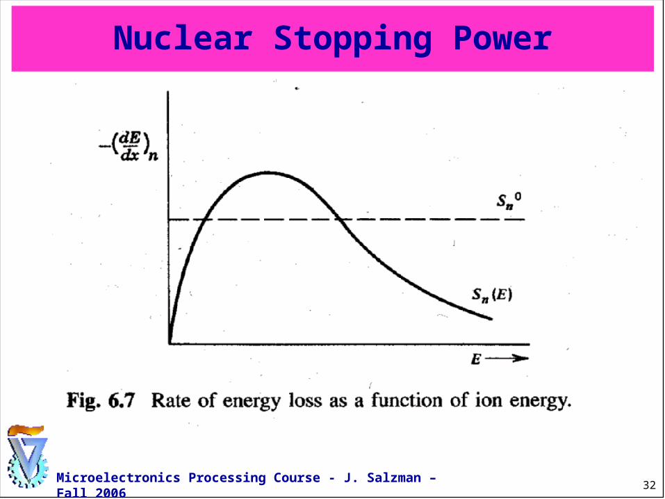
Nuclear Stopping Power
33
Microelectronics Processing Course - J. Salzman – Fall 2006
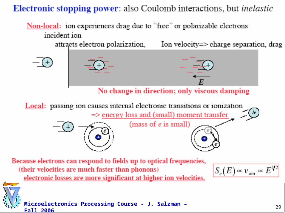
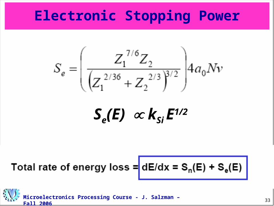
Electronic Stopping Power
Se(E) kSi E1/2
34
Microelectronics Processing Course - J. Salzman – Fall 2006
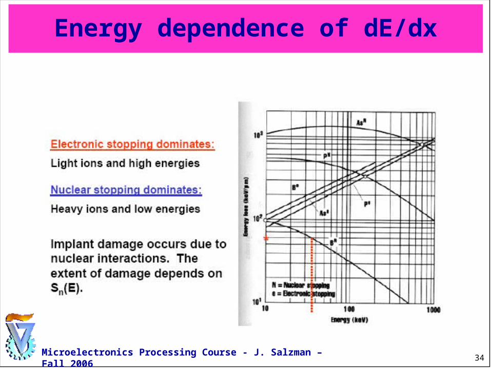
Energy dependence of dE/dx
35
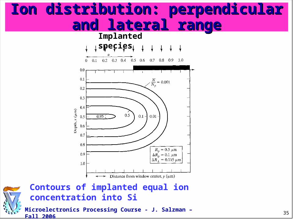
Microelectronics Processing Course - J. Salzman – Fall 2006
Ion distribution: perpendicular and Ion distribution: perpendicular and lateral rangelateral range
Implanted species
Contours of implanted equal ion concentration into Si
36
Microelectronics Processing Course - J. Salzman – Fall 2006
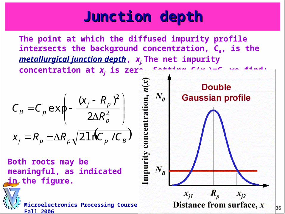
Junction depthJunction depth
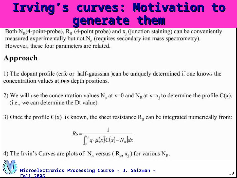
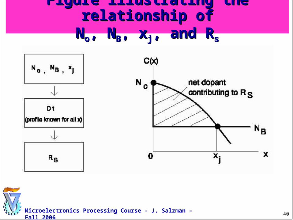
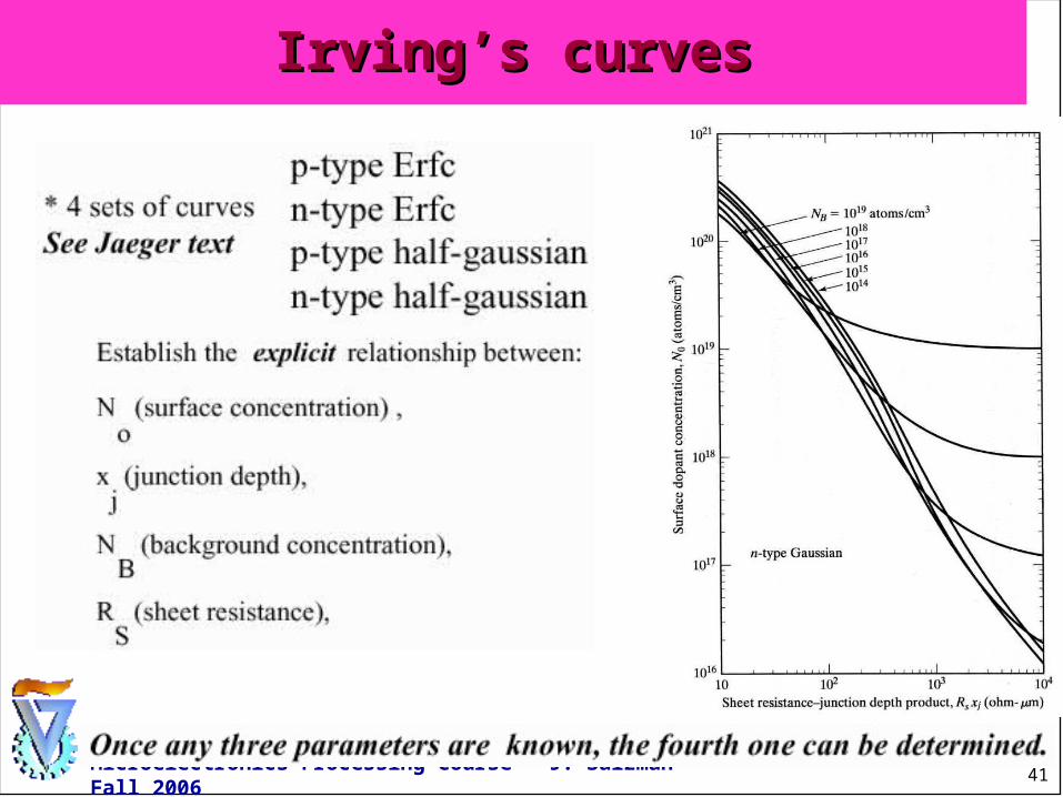
The point at which the diffused impurity profile intersects the background concentration, CB, is the metallurgical junction depth, xj. The net impurity concentration at xj is zero. Setting C(xj)=CB we find:
Bpppj
p
pjpB
CCRRx
R
RxCC
/ln2
2
)(exp
2
2
Both roots may be meaningful, as indicated in the figure.
37
Microelectronics Processing Course - J. Salzman – Fall 2006
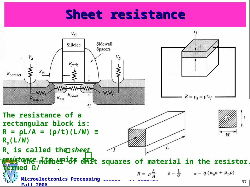
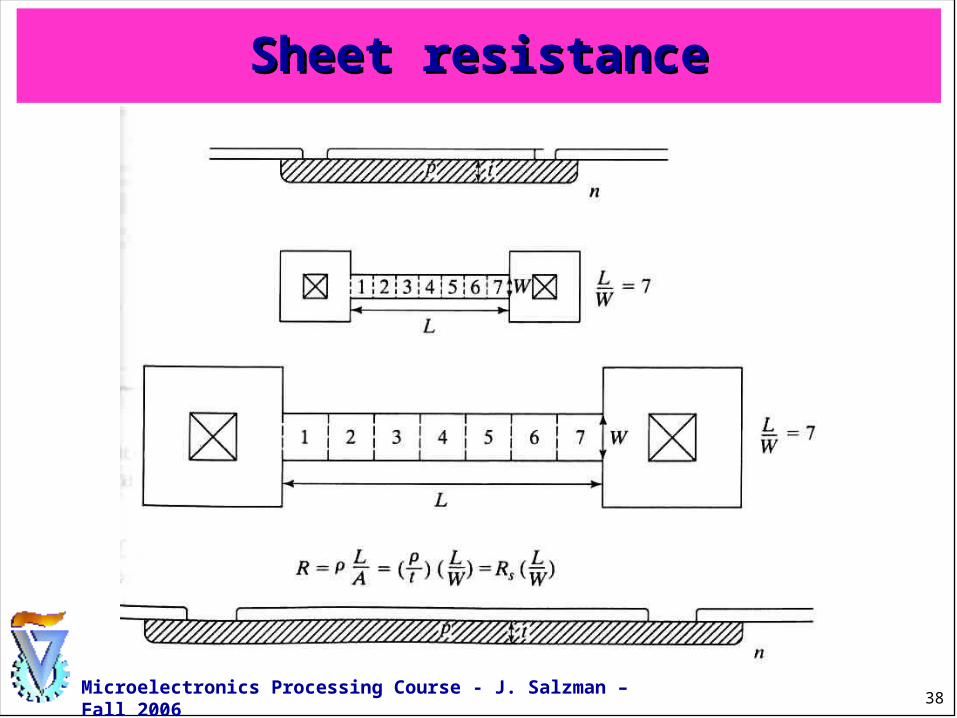
Sheet resistanceSheet resistance
The resistance of a rectangular block is:R = ρL/A = (ρ/t)(L/W) ≡ Rs(L/W)
Rs is called the sheet resistance. Its units are termed Ω/ .
L/W is the number of unit squares of material in the resistor.
38
Microelectronics Processing Course - J. Salzman – Fall 2006
Sheet resistanceSheet resistance
39
Microelectronics Processing Course - J. Salzman – Fall 2006
Irving’s curves: Motivation to generate Irving’s curves: Motivation to generate themthem
40
Microelectronics Processing Course - J. Salzman – Fall 2006
Figure illustrating the relationship ofFigure illustrating the relationship ofNNoo, N, NBB, x, xjj, and R, and Rss
41
Microelectronics Processing Course - J. Salzman – Fall 2006
Irving’s curvesIrving’s curves
42
Microelectronics Processing Course - J. Salzman – Fall 2006
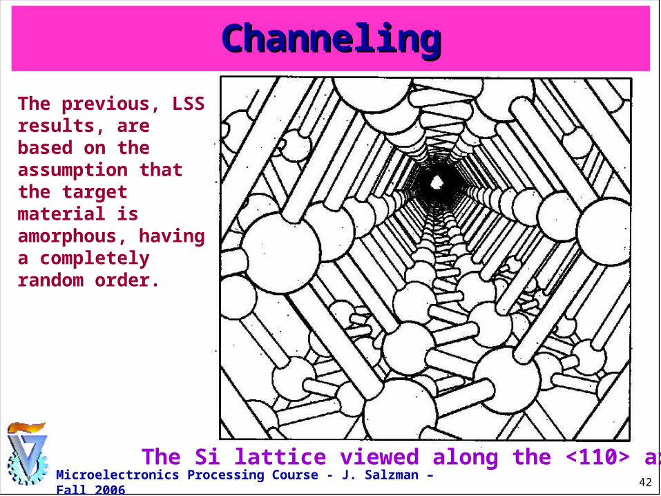
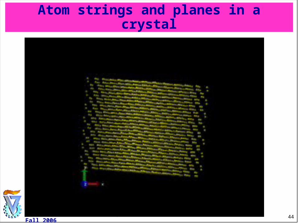
ChannelingChanneling
The previous, LSS results, are based on the assumption that the target material is amorphous, having a completely random order.
The Si lattice viewed along the <110> axis.

43
Microelectronics Processing Course - J. Salzman – Fall 2006
44
Microelectronics Processing Course - J. Salzman – Fall 2006
Atom strings and planes in a crystal
45
Microelectronics Processing Course - J. Salzman – Fall 2006
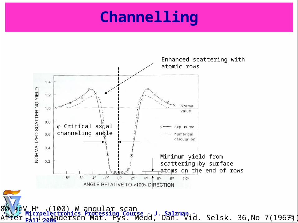
Channelling
480 keV H+ →(100) W angular scan (After J.U. Andersen Mat. Fys. Medd, Dan. Vid. Selsk. 36,No 7(1967))
Enhanced scattering with atomic rows
Minimum yield from scattering by surface atoms on the end of rows
Critical axial channeling angle
46
Microelectronics Processing Course - J. Salzman – Fall 2006
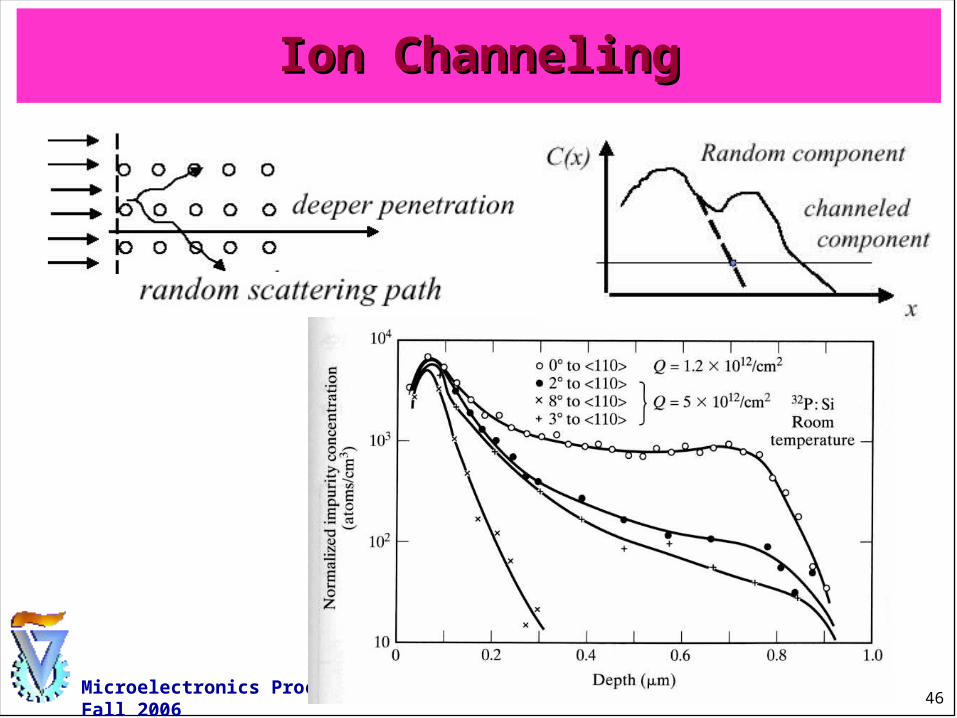
Ion ChannelingIon Channeling
47
Microelectronics Processing Course - J. Salzman – Fall 2006
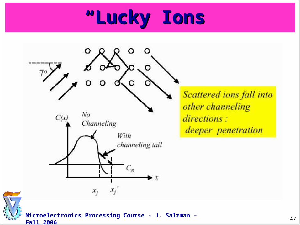
““Lucky Ions”Lucky Ions”
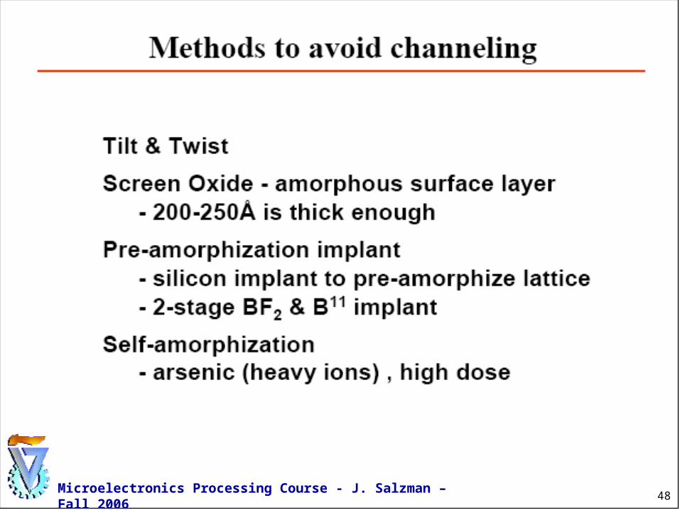
48
Microelectronics Processing Course - J. Salzman – Fall 2006
49
Microelectronics Processing Course - J. Salzman – Fall 2006
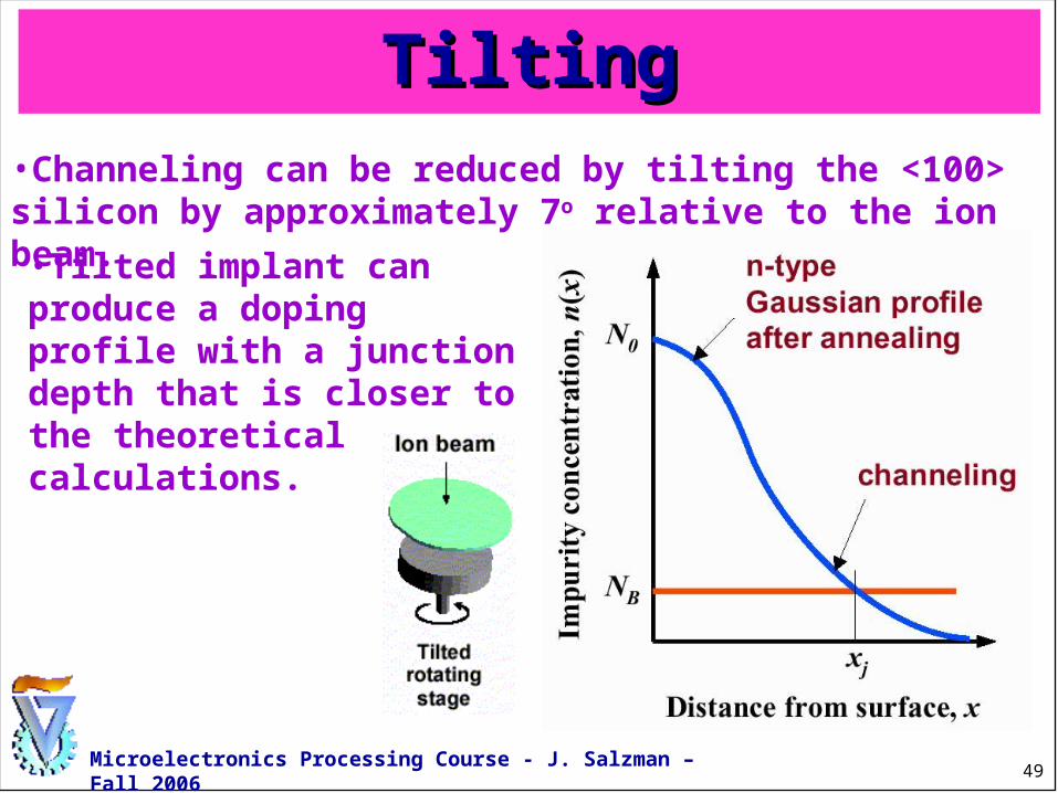
TiltingTilting•Channeling can be reduced by tilting the <100> silicon by approximately 7o relative to the ion beam.
•Tilted implant can produce a doping profile with a junction depth that is closer to the theoretical calculations.
50
Microelectronics Processing Course - J. Salzman – Fall 2006
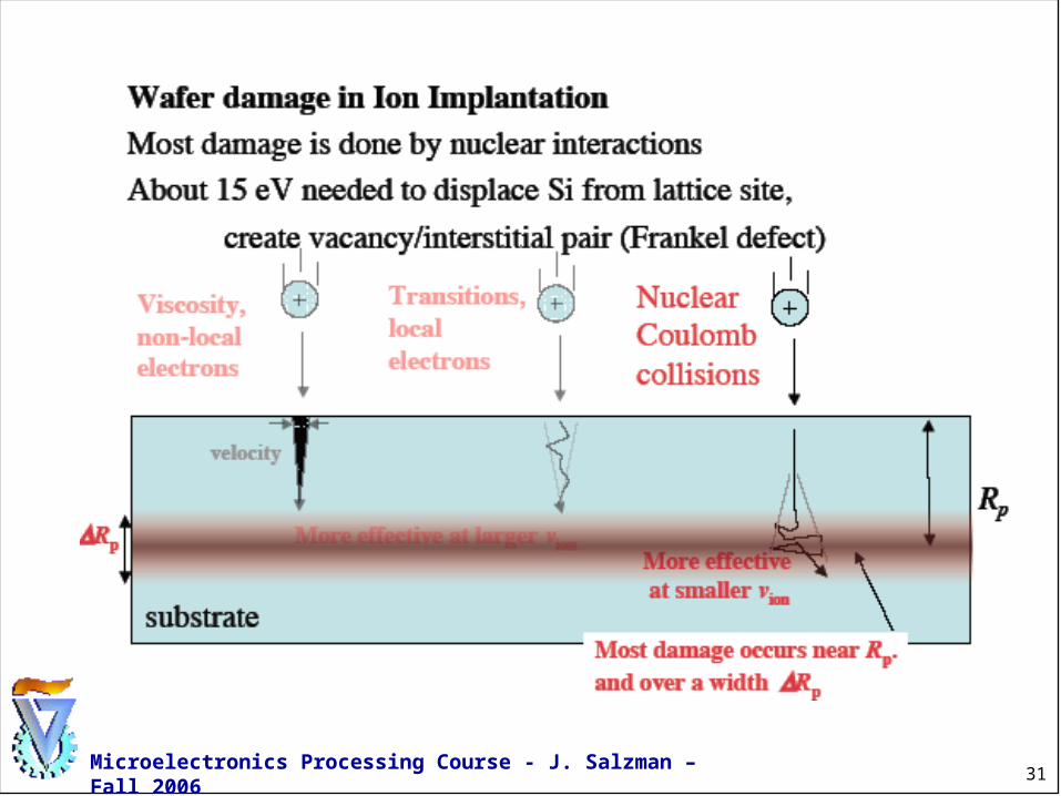
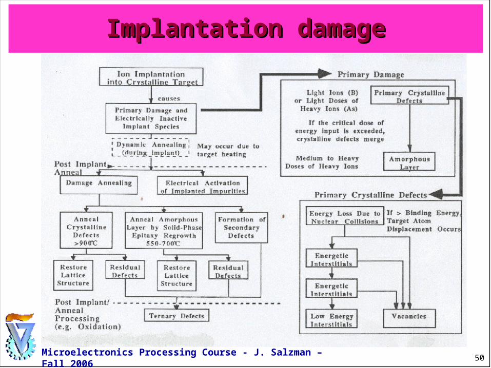
Implantation damageImplantation damage

51
Microelectronics Processing Course - J. Salzman – Fall 2006
Implantation damage - AmorphizationImplantation damage - Amorphization
A plot of the dose required to form an amorphous layer on silicon versus reciprocal target temperature.
52
Microelectronics Processing Course - J. Salzman – Fall 2006
Post Implant Anneal
Electrical activation of implanted Impurities
Annealing of primary crystalline defect damage
Annealing of amorphous layers Dynamic annealing effects Diffusion of implanted impurities
53
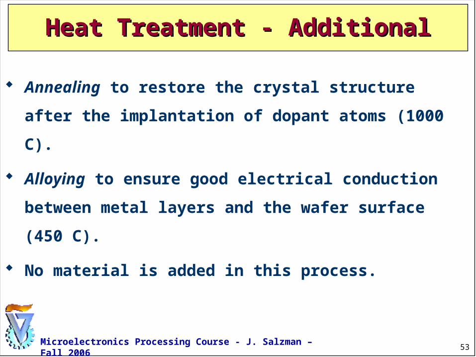
Microelectronics Processing Course - J. Salzman – Fall 2006
Heat Treatment - AdditionalHeat Treatment - Additional
Annealing to restore the crystal structure after the
implantation of dopant atoms (1000 C).
Alloying to ensure good electrical conduction between
metal layers and the wafer surface (450 C).
No material is added in this process.
54
Microelectronics Processing Course - J. Salzman – Fall 2006
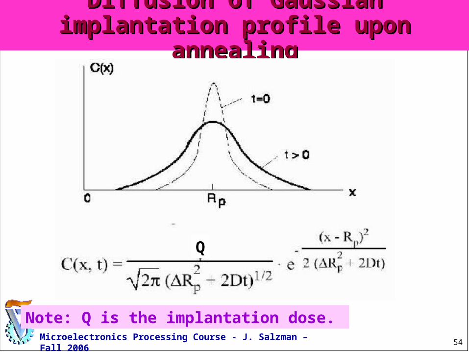
Diffusion of Gaussian implantation Diffusion of Gaussian implantation profile upon annealingprofile upon annealing
Note: Q is the implantation dose.
Q
55
Microelectronics Processing Course - J. Salzman – Fall 2006
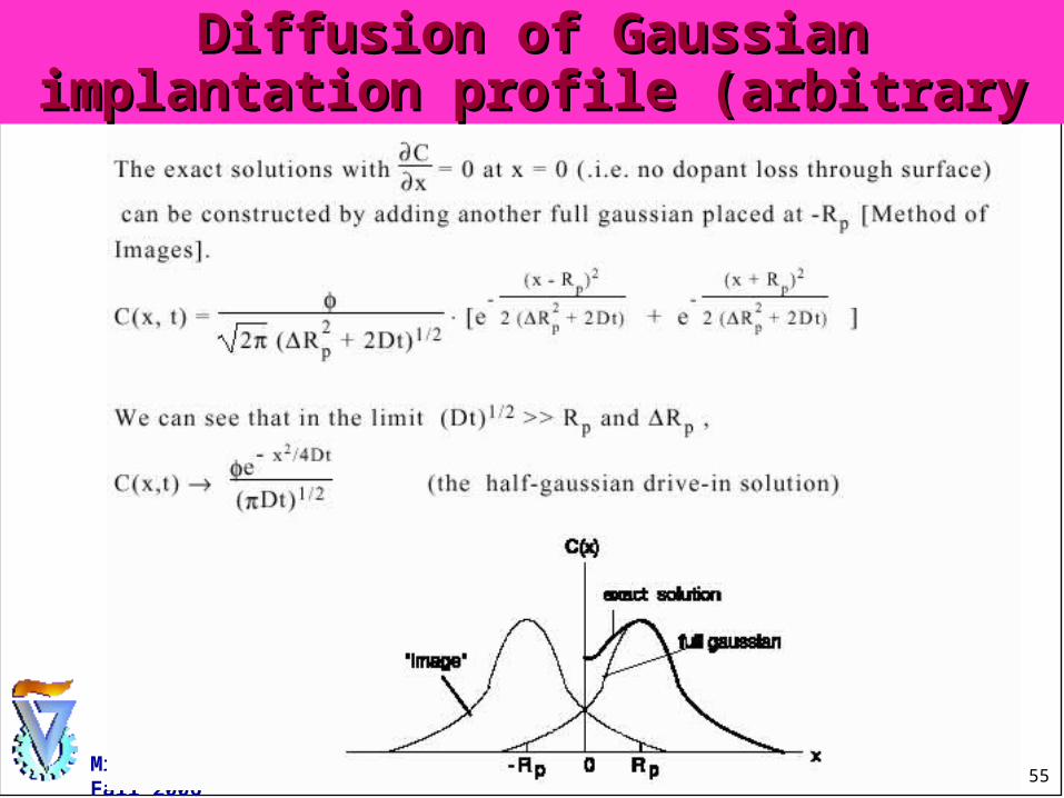
Diffusion of Gaussian implantation Diffusion of Gaussian implantation profile (arbitrary Rprofile (arbitrary Rpp))
56
Microelectronics Processing Course - J. Salzman – Fall 2006
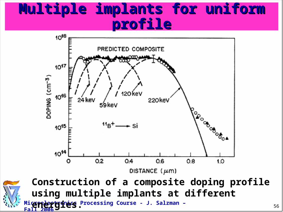
Multiple implants for uniform profileMultiple implants for uniform profile
Construction of a composite doping profile using multiple implants at different energies.
57
Microelectronics Processing Course - J. Salzman – Fall 2006
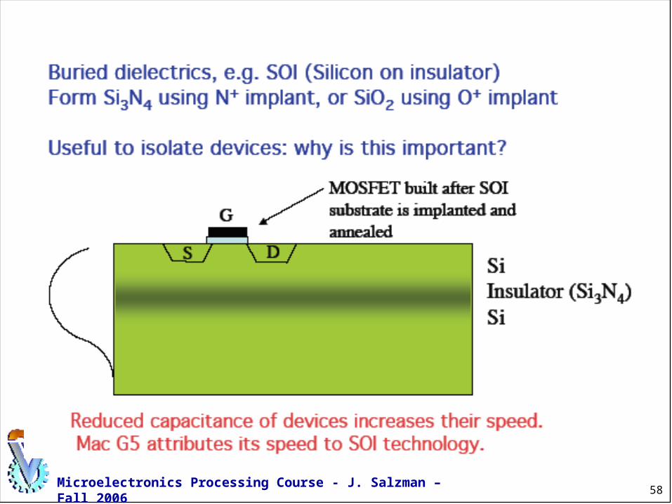
Additional featuresAdditional featuresWafer annealing:
Damage removed by annealing the wafer at high temperature for a short period; implanted impurity atoms are "activated".
Proton isolation Hydrogen ions are used to deliberately change the crystal and convert it into electrically insulating material.
Predeposition by ion implantation Ion implantation predeposition of a fixed number of impurities into the semiconductor in preference to predeposition by thermal diffusion
Threshold voltage adjustment:By shallow ion implants through the SiO2 gate oxide layer
58
Microelectronics Processing Course - J. Salzman – Fall 2006