Embed Size (px)
Citation preview
1Technion- Microelectronic Processing – Joseph Salzman – Fall 2006
Microelectronics Processing Microelectronics Processing EtchingEtching
2Technion- Microelectronic Processing – Joseph Salzman – Fall 2006
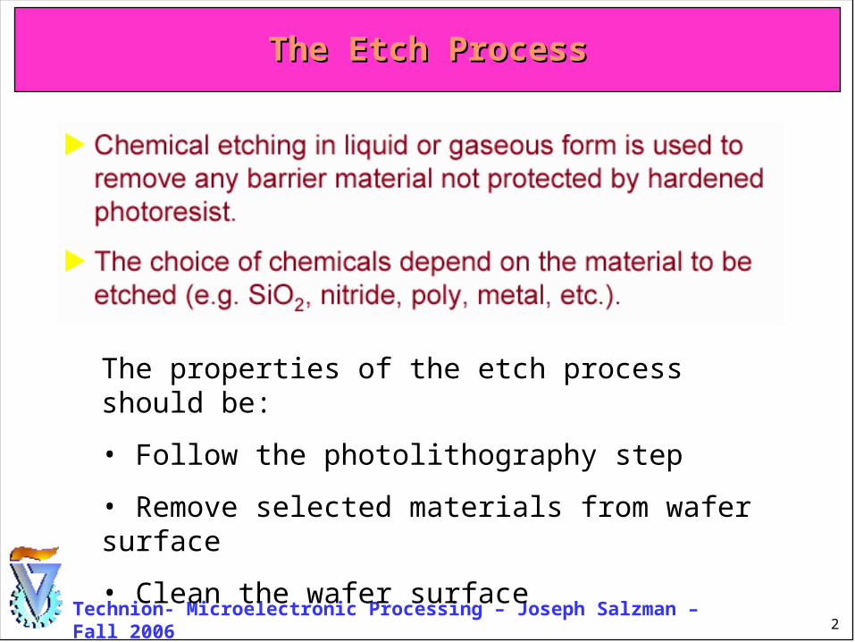
The Etch ProcessThe Etch Process
The properties of the etch process should be:
• Follow the photolithography step
• Remove selected materials from wafer surface
• Clean the wafer surface
3Technion- Microelectronic Processing – Joseph Salzman – Fall 2006
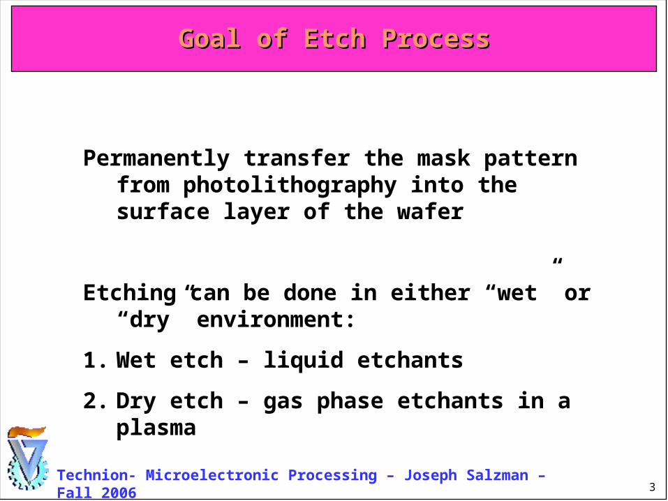
Permanently transfer the mask pattern from photolithography into the surface layer of the wafer
Etching can be done in either “wet” or “dry” environment:
1. Wet etch – liquid etchants
2. Dry etch – gas phase etchants in a plasma
Goal of Etch ProcessGoal of Etch Process
4Technion- Microelectronic Processing – Joseph Salzman – Fall 2006
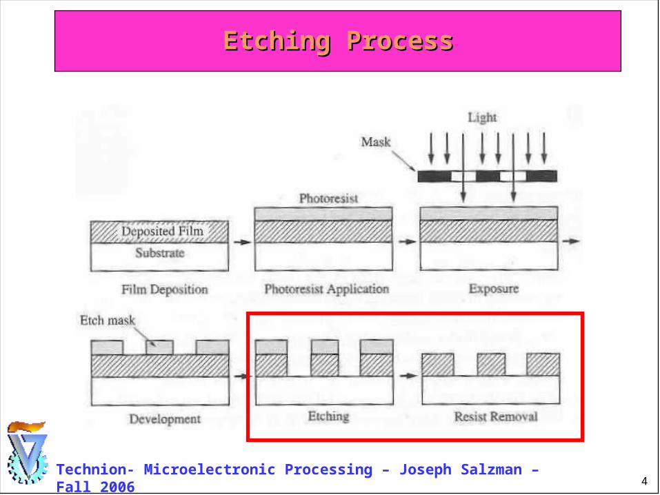
Etching ProcessEtching Process
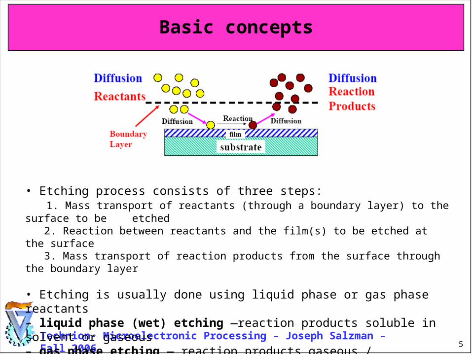
5Technion- Microelectronic Processing – Joseph Salzman – Fall 2006
Basic concepts
• Etching process consists of three steps: 1. Mass transport of reactants (through a boundary layer) to the surface to be etched 2. Reaction between reactants and the film(s) to be etched at the surface 3. Mass transport of reaction products from the surface through the boundary layer
• Etching is usually done using liquid phase or gas phase reactants– liquid phase (wet) etching —reaction products soluble in solvent or gaseous– gas phase etching — reaction products gaseous / sublimation temperature
6Technion- Microelectronic Processing – Joseph Salzman – Fall 2006
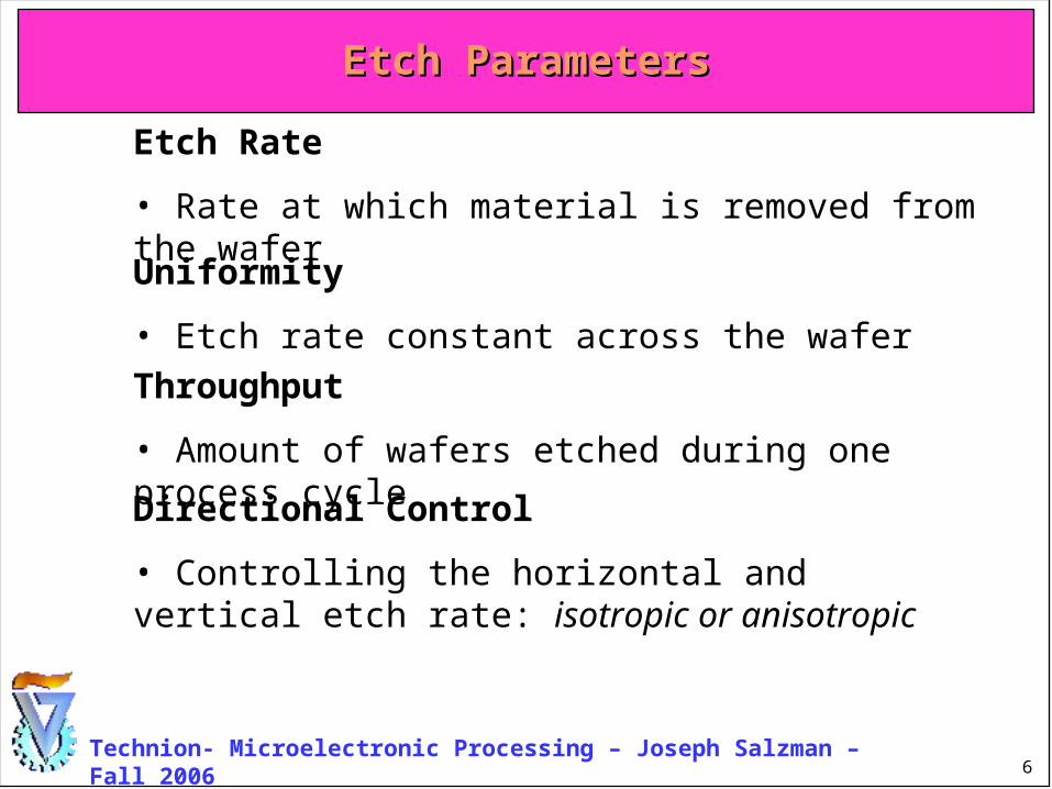
Etch Rate
• Rate at which material is removed from the wafer
Uniformity
• Etch rate constant across the wafer
Throughput
• Amount of wafers etched during one process cycle
Directional Control
• Controlling the horizontal and vertical etch rate: isotropic or anisotropic
Etch ParametersEtch Parameters
7Technion- Microelectronic Processing – Joseph Salzman – Fall 2006
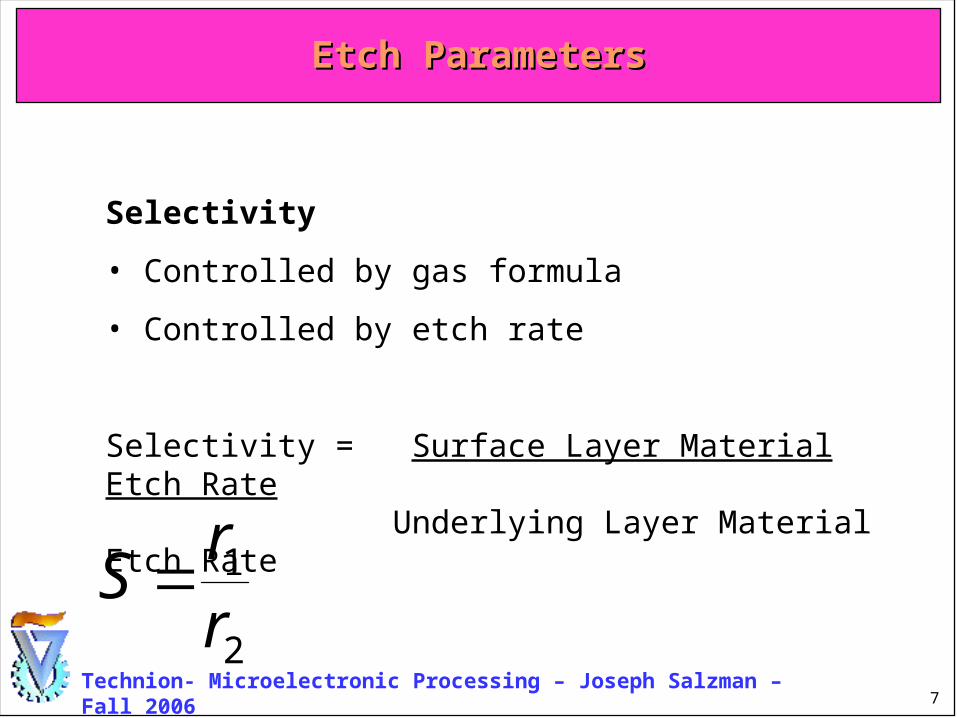
Selectivity
• Controlled by gas formula
• Controlled by etch rate
Selectivity = Surface Layer Material Etch Rate Underlying Layer Material Etch Rate
Etch ParametersEtch Parameters
2
1
rr
S
8Technion- Microelectronic Processing – Joseph Salzman – Fall 2006
Figures of merit
9Technion- Microelectronic Processing – Joseph Salzman – Fall 2006
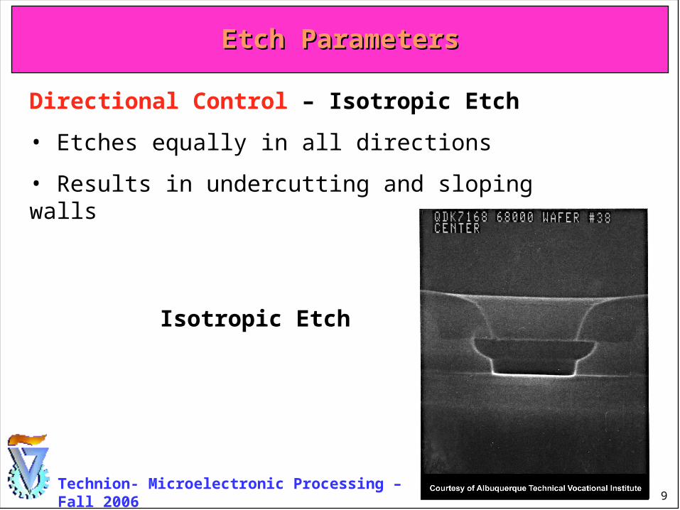
Directional Control – Isotropic Etch
• Etches equally in all directions
• Results in undercutting and sloping walls
Etch ParametersEtch Parameters
Isotropic Etch
10Technion- Microelectronic Processing – Joseph Salzman – Fall 2006
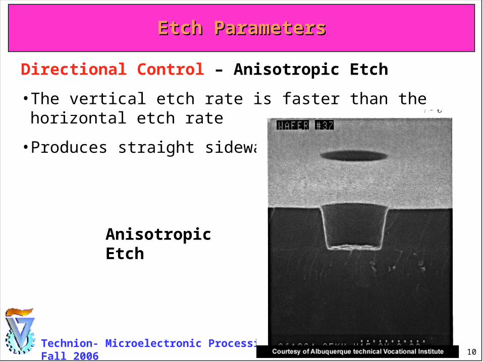
Directional Control – Anisotropic Etch
• The vertical etch rate is faster than the horizontal etch rate
• Produces straight sidewalls
Etch ParametersEtch Parameters
Anisotropic Etch
11Technion- Microelectronic Processing – Joseph Salzman – Fall 2006
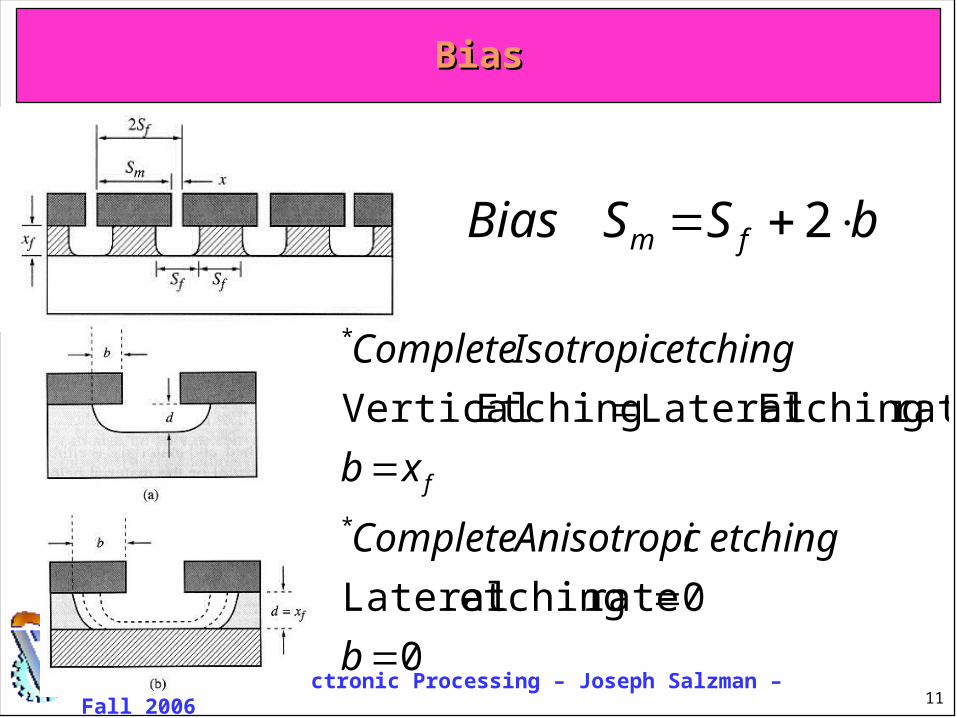
BiasBias
bSSBias fm 2
0
0rate etching Lateral
rate Etching LateralEtching Vertical
*
*
b
etchingcAnisotropiComplete
xb
etchingIsotropicComplete
f
12Technion- Microelectronic Processing – Joseph Salzman – Fall 2006
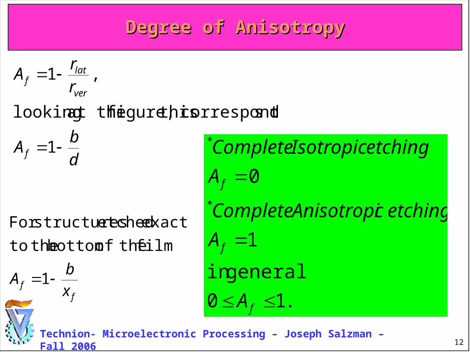
Degree of AnisotropyDegree of Anisotropy
db
A
r
rA
f
ver
latf
1
toscorrespond thisfigure, at the looking
,1
.10
generalin
1
0*
*
f
f
f
A
A
etchingcAnisotropiComplete
A
etchingIsotropicComplete
ff x
bA 1
film theof bottom theto
exactly etched structuresFor
13Technion- Microelectronic Processing – Joseph Salzman – Fall 2006
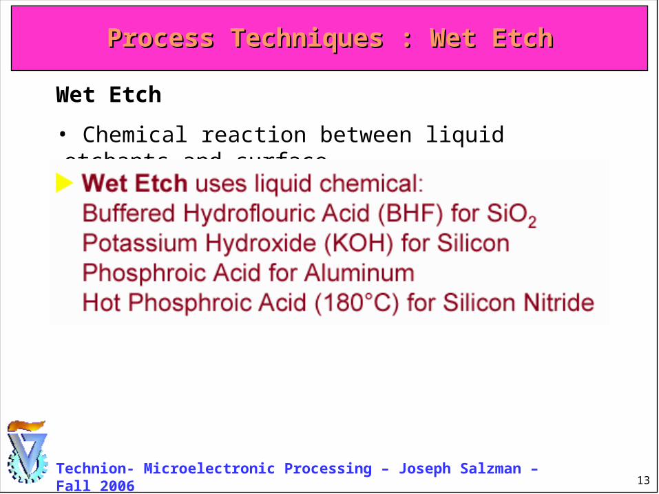
Wet Etch
• Chemical reaction between liquid etchants and surface
Process Techniques : Wet EtchProcess Techniques : Wet Etch
14Technion- Microelectronic Processing – Joseph Salzman – Fall 2006
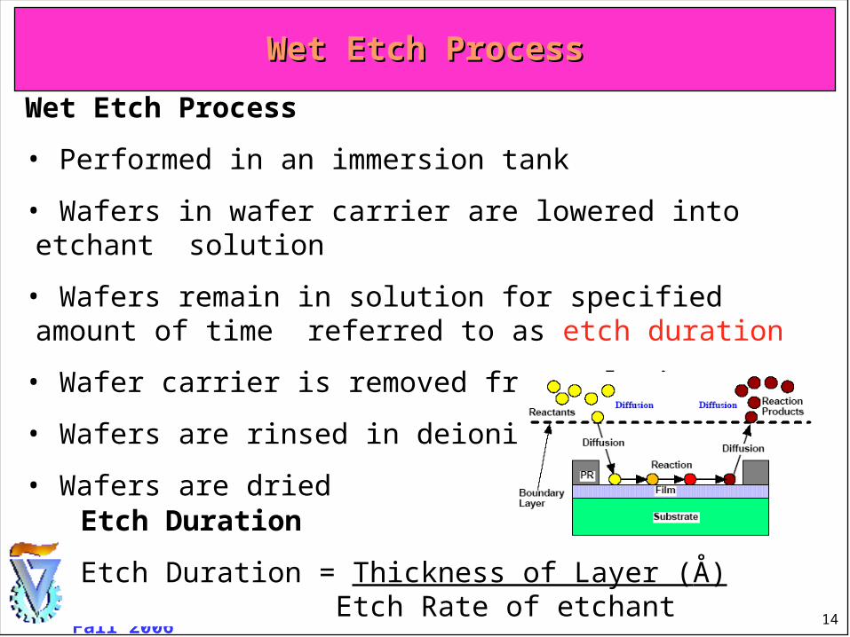
Wet Etch Process
• Performed in an immersion tank
• Wafers in wafer carrier are lowered into etchant solution
• Wafers remain in solution for specified amount of time .referred to as etch duration
• Wafer carrier is removed from solution
• Wafers are rinsed in deionized water
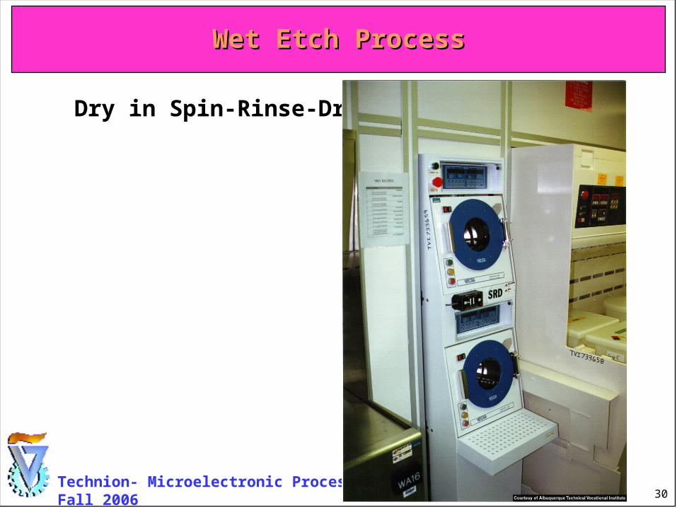
• Wafers are dried
Wet Etch ProcessWet Etch Process
Etch Duration
Etch Duration = Thickness of Layer (Å) Etch Rate of etchant
15Technion- Microelectronic Processing – Joseph Salzman – Fall 2006
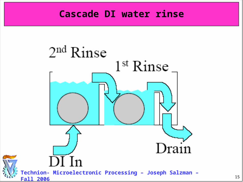
Cascade DI water rinse
16Technion- Microelectronic Processing – Joseph Salzman – Fall 2006
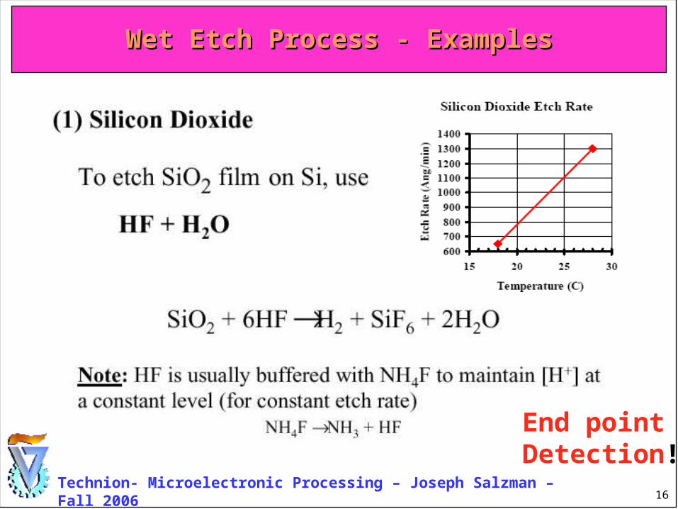
Wet Etch Process - ExamplesWet Etch Process - Examples
End pointDetection!
17Technion- Microelectronic Processing – Joseph Salzman – Fall 2006
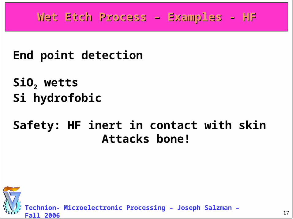
Wet Etch Process – Examples - HFWet Etch Process – Examples - HF
End point detection
SiO2 wettsSi hydrofobic
Safety: HF inert in contact with skin Attacks bone!
18Technion- Microelectronic Processing – Joseph Salzman – Fall 2006
Wet Etch Process - ExamplesWet Etch Process - Examples
19Technion- Microelectronic Processing – Joseph Salzman – Fall 2006
Wet Etch Process - ExamplesWet Etch Process - Examples
20Technion- Microelectronic Processing – Joseph Salzman – Fall 2006
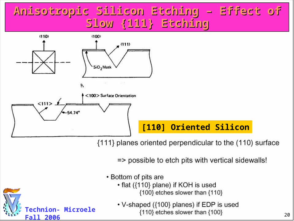
Anisotropic Silicon Etching – Effect of Slow Anisotropic Silicon Etching – Effect of Slow {111} Etching{111} Etching
[110] Oriented Silicon
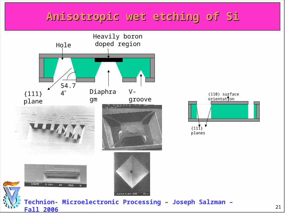
21Technion- Microelectronic Processing – Joseph Salzman – Fall 2006
Anisotropic wet etching of SiAnisotropic wet etching of Si
{111} planes
(110) surface orientation
Heavily borondoped regionHole
Diaphragm V-groove{111} planes
54.74
22Technion- Microelectronic Processing – Joseph Salzman – Fall 2006
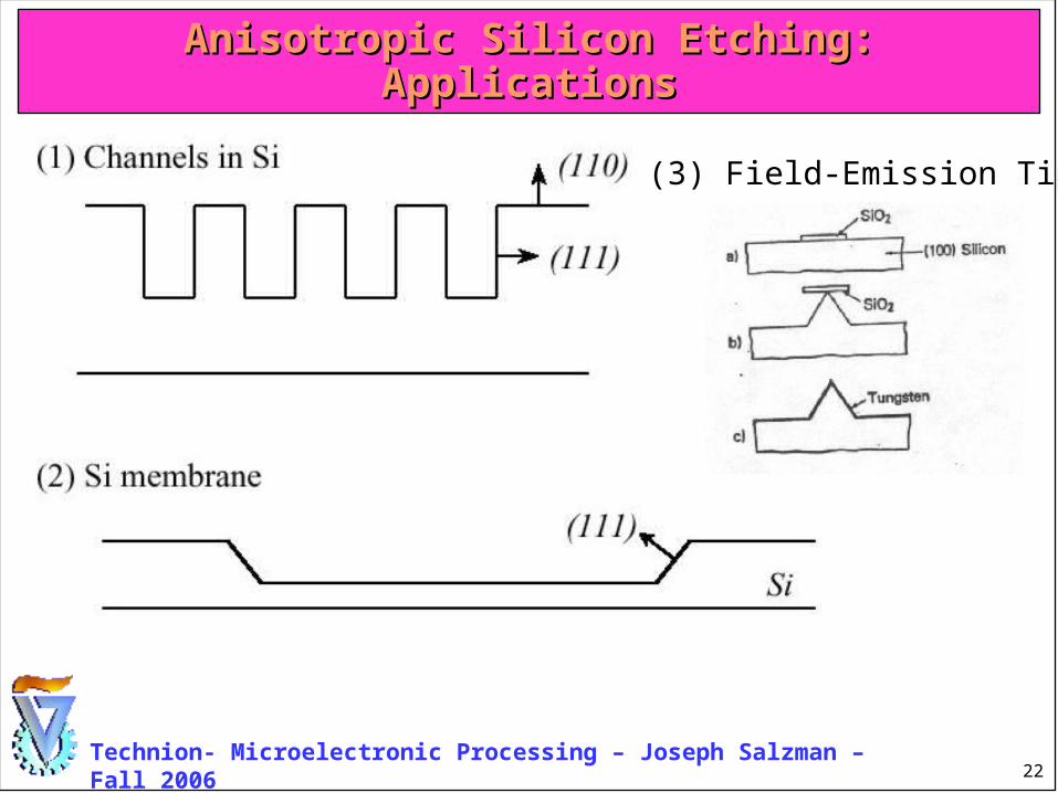
Anisotropic Silicon Etching: ApplicationsAnisotropic Silicon Etching: Applications
(3) Field-Emission Tips
23Technion- Microelectronic Processing – Joseph Salzman – Fall 2006
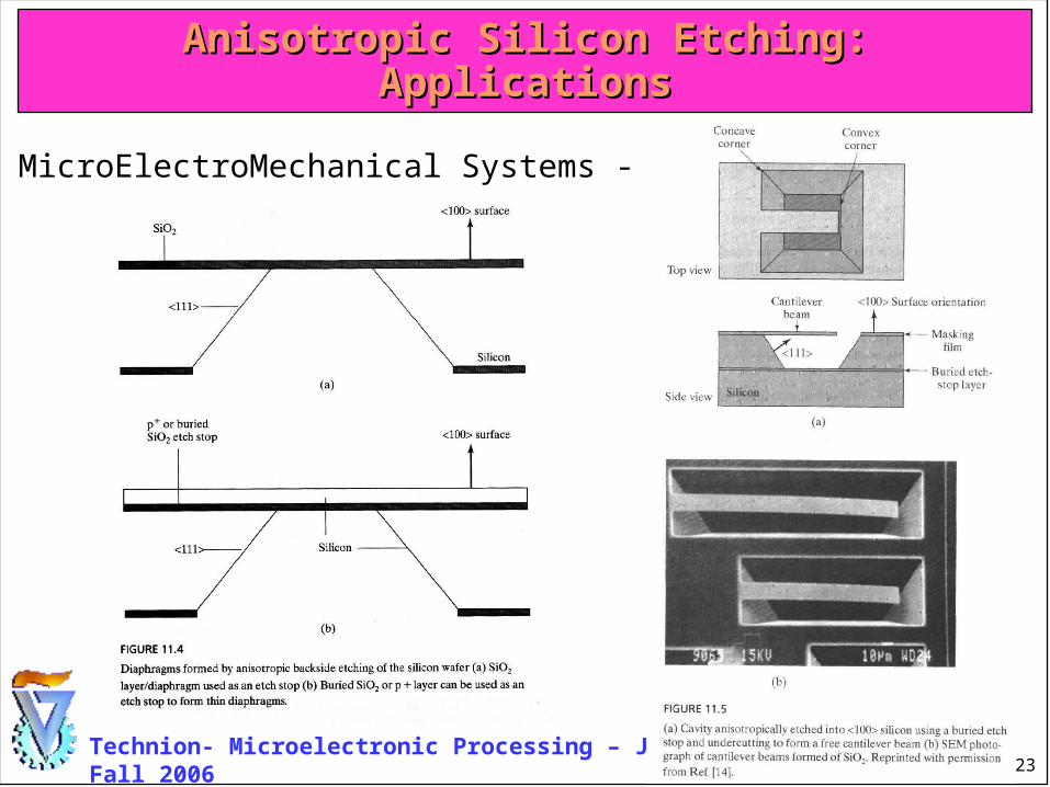
Anisotropic Silicon Etching: ApplicationsAnisotropic Silicon Etching: Applications
(4) MicroElectroMechanical Systems - MEMS
24Technion- Microelectronic Processing – Joseph Salzman – Fall 2006
Etching selectively by doping
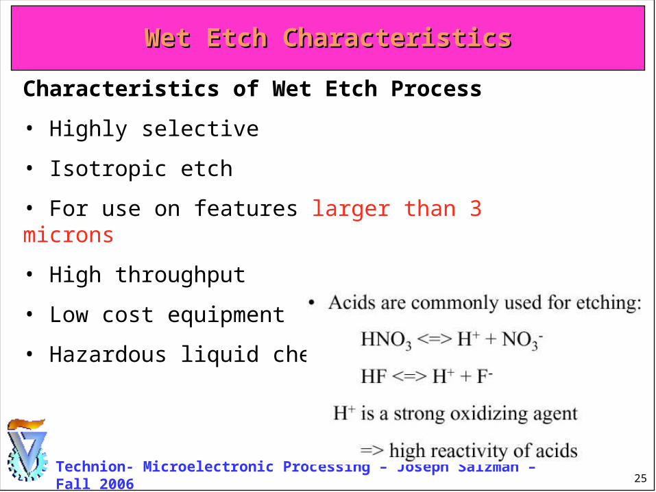
25Technion- Microelectronic Processing – Joseph Salzman – Fall 2006
Characteristics of Wet Etch Process
• Highly selective
• Isotropic etch
• For use on features larger than 3 microns
• High throughput
• Low cost equipment
• Hazardous liquid chemicals
Wet Etch CharacteristicsWet Etch Characteristics
26Technion- Microelectronic Processing – Joseph Salzman – Fall 2006
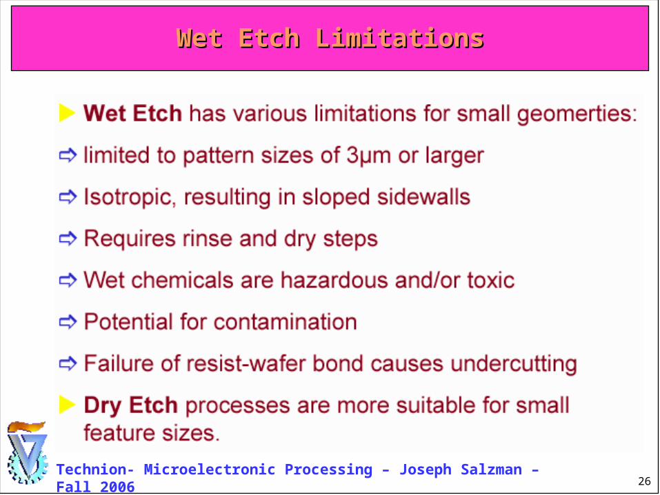
Wet Etch LimitationsWet Etch Limitations
27Technion- Microelectronic Processing – Joseph Salzman – Fall 2006
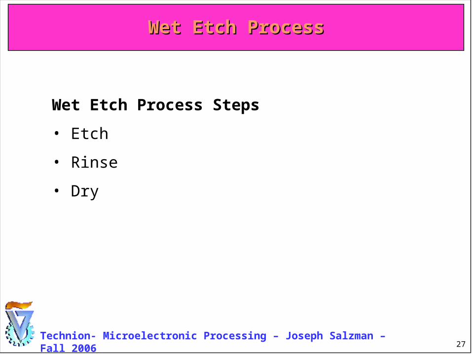
Wet Etch Process Steps
• Etch
• Rinse
• Dry
Wet Etch ProcessWet Etch Process
28Technion- Microelectronic Processing – Joseph Salzman – Fall 2006
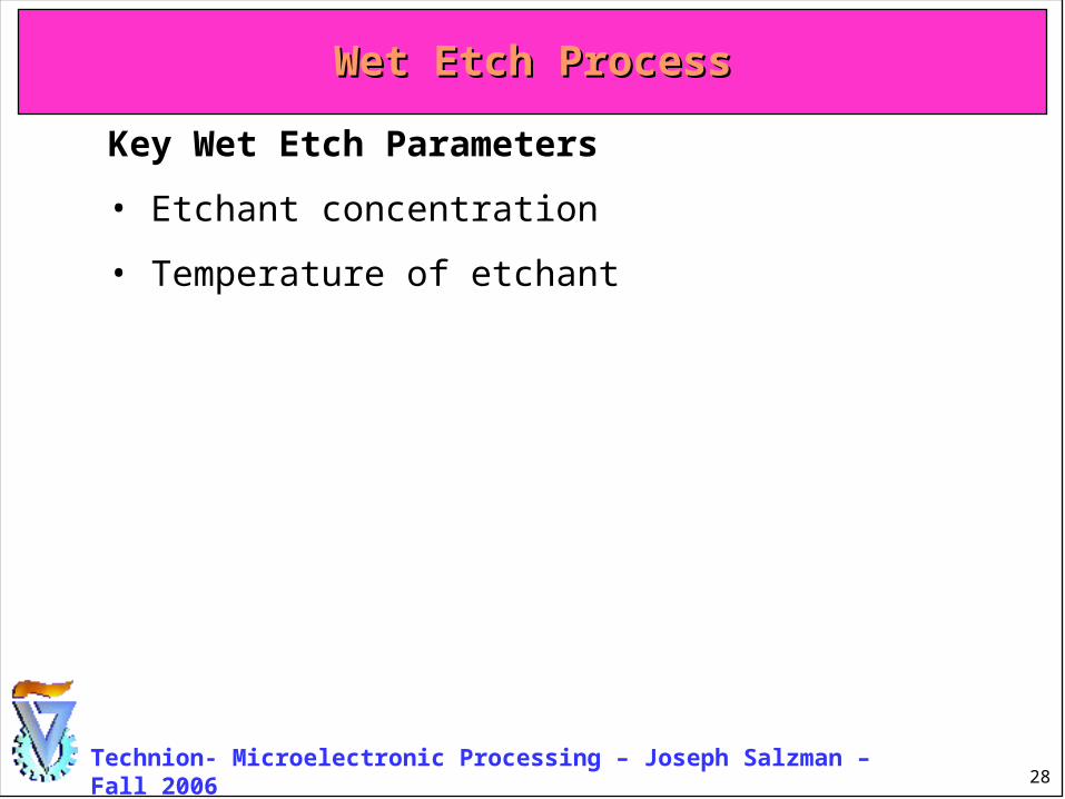
Key Wet Etch Parameters
• Etchant concentration
• Temperature of etchant
Wet Etch ProcessWet Etch Process
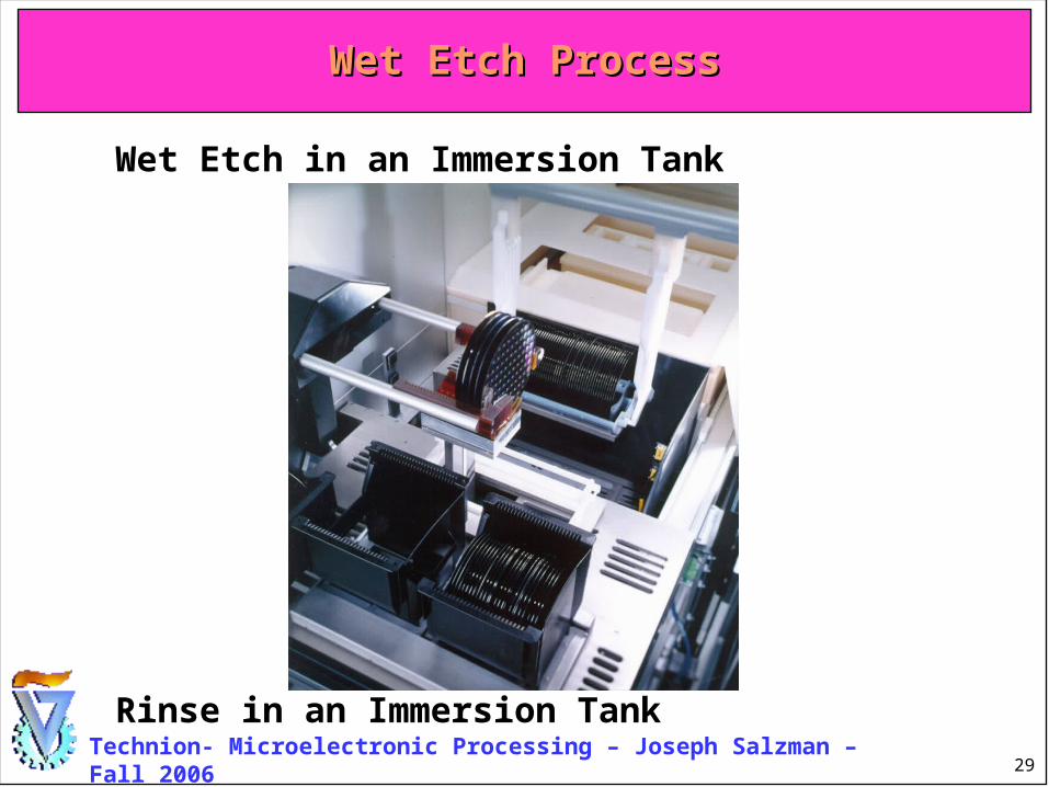
29Technion- Microelectronic Processing – Joseph Salzman – Fall 2006
Wet Etch in an Immersion Tank
Wet Etch ProcessWet Etch Process
Rinse in an Immersion Tank
30Technion- Microelectronic Processing – Joseph Salzman – Fall 2006
Dry in Spin-Rinse-Dryer
Wet Etch ProcessWet Etch Process
31Technion- Microelectronic Processing – Joseph Salzman – Fall 2006
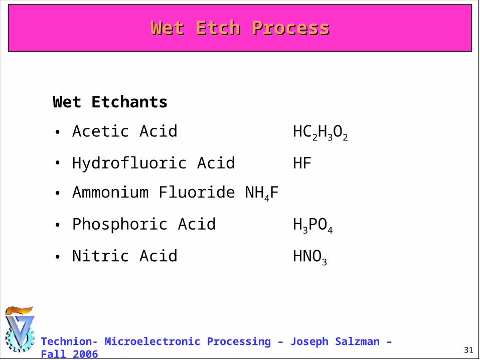
Wet Etchants
• Acetic Acid HC2H3O2
• Hydrofluoric Acid HF
• Ammonium Fluoride NH4F
• Phosphoric Acid H3PO4
• Nitric Acid HNO3
Wet Etch ProcessWet Etch Process
32Technion- Microelectronic Processing – Joseph Salzman – Fall 2006
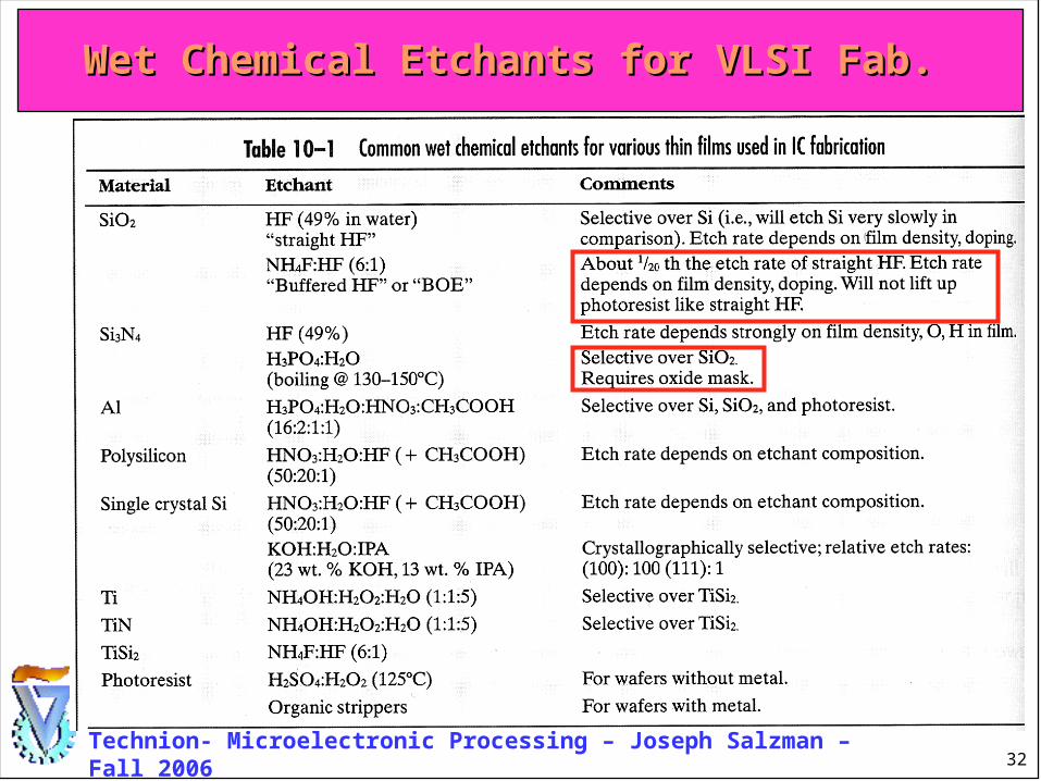
Wet Chemical Etchants for VLSI Fab. Wet Chemical Etchants for VLSI Fab.
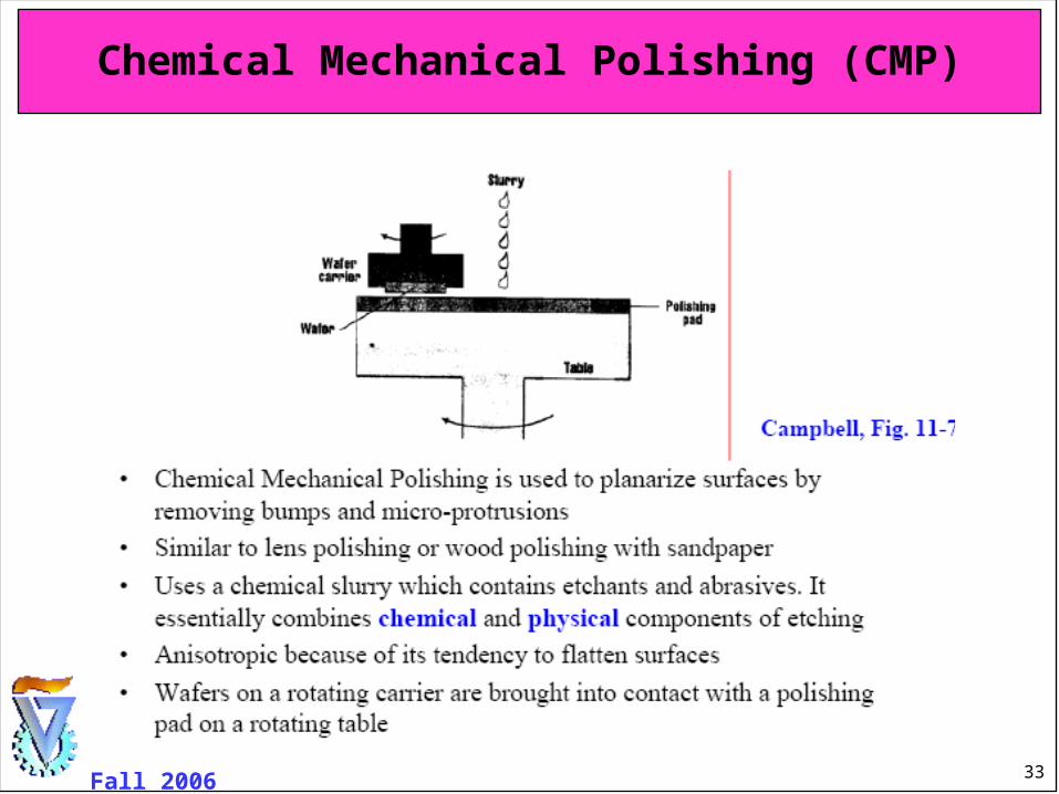
33Technion- Microelectronic Processing – Joseph Salzman – Fall 2006
Chemical Mechanical Polishing (CMP)
34Technion- Microelectronic Processing – Joseph Salzman – Fall 2006
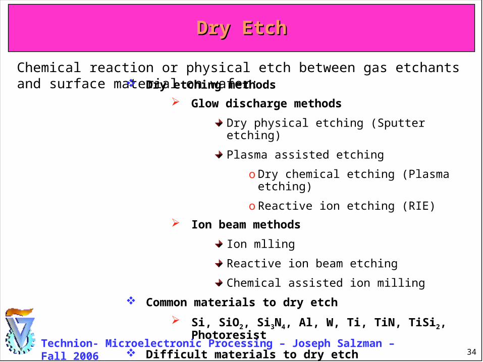
Dry EtchDry Etch
Chemical reaction or physical etch between gas.etchants and surface material on wafer: Dry etching methods
Glow discharge methods
Dry physical etching (Sputter etching)
Plasma assisted etching
o Dry chemical etching (Plasma etching)
o Reactive ion etching (RIE)
Ion beam methods
Ion mlling
Reactive ion beam etching
Chemical assisted ion milling
Common materials to dry etch
Si, SiO2, Si3N4, Al, W, Ti, TiN, TiSi2, Photoresist
Difficult materials to dry etch
Fe, Ni, Co, Cu, Al2O3, LiNbO3, etc.
35Technion- Microelectronic Processing – Joseph Salzman – Fall 2006
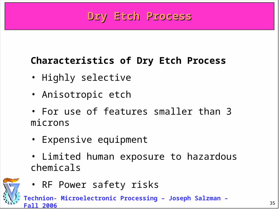
Characteristics of Dry Etch Process
• Highly selective
• Anisotropic etch
• For use of features smaller than 3 microns
• Expensive equipment
• Limited human exposure to hazardous chemicals
• RF Power safety risks
Dry Etch ProcessDry Etch Process
36Technion- Microelectronic Processing – Joseph Salzman – Fall 2006
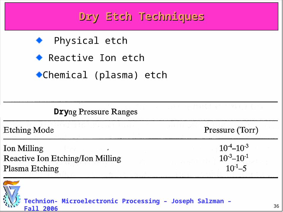
Dry Etch TechniquesDry Etch Techniques
Physical etch
Reactive Ion etch
Chemical (plasma) etch
Dry
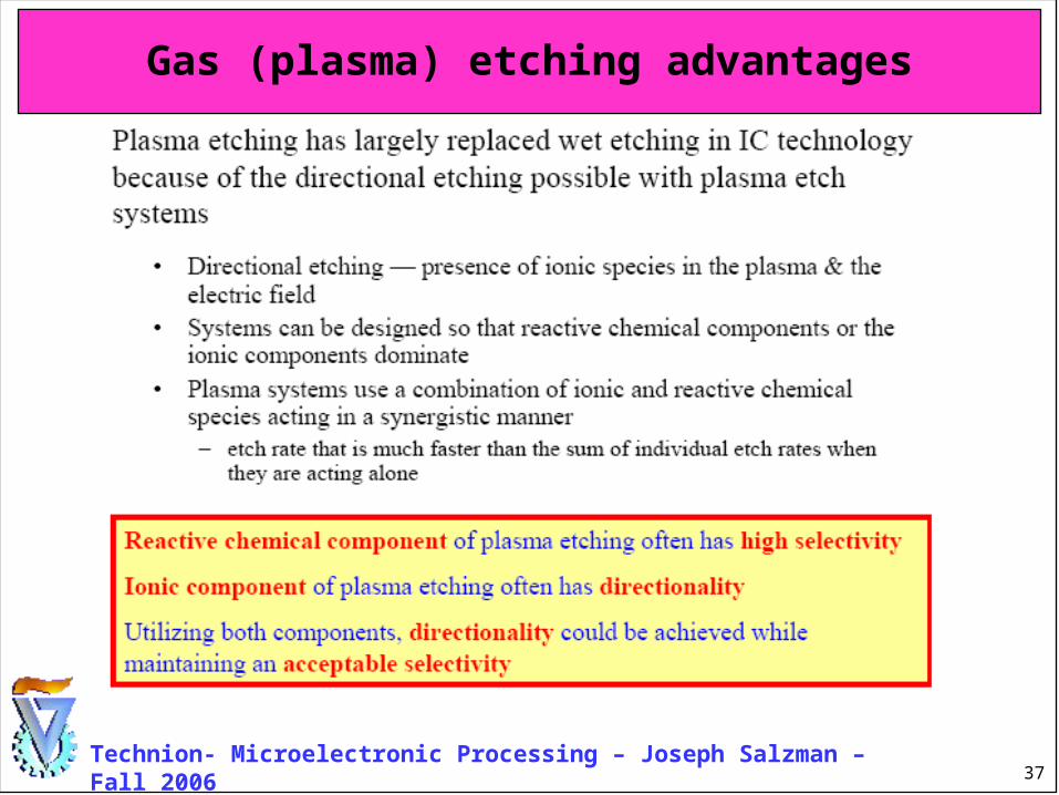
37Technion- Microelectronic Processing – Joseph Salzman – Fall 2006
Gas (plasma) etching advantages
38Technion- Microelectronic Processing – Joseph Salzman – Fall 2006
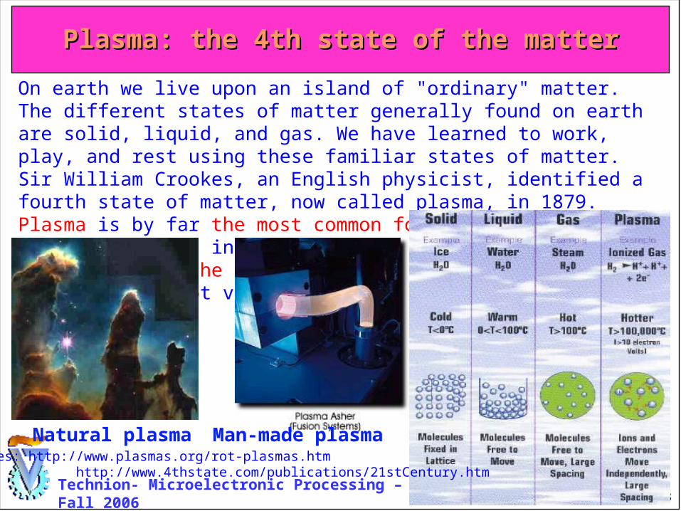
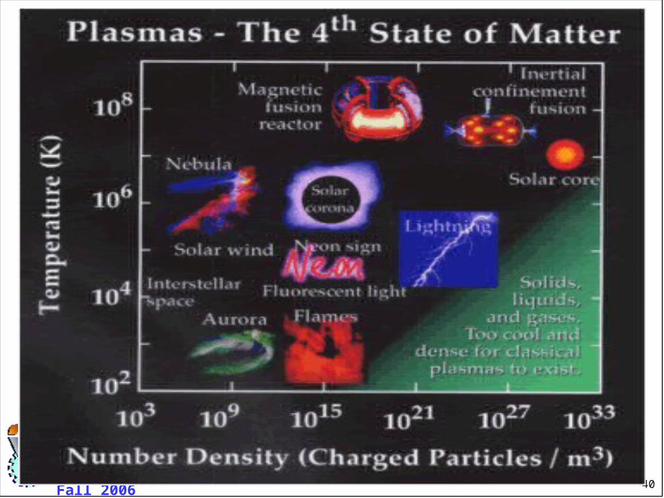
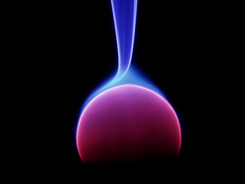
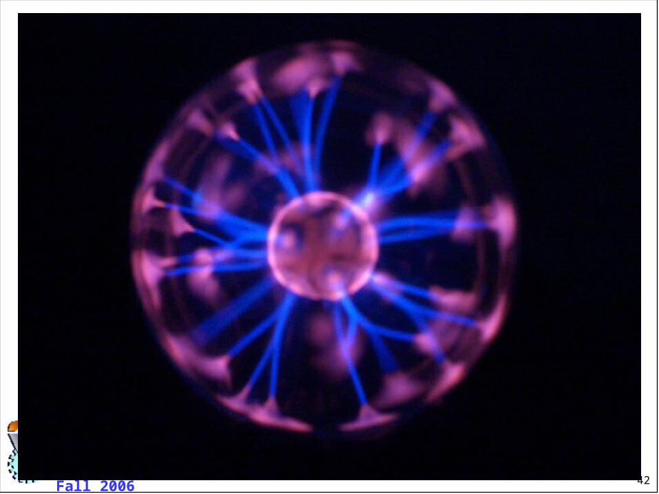
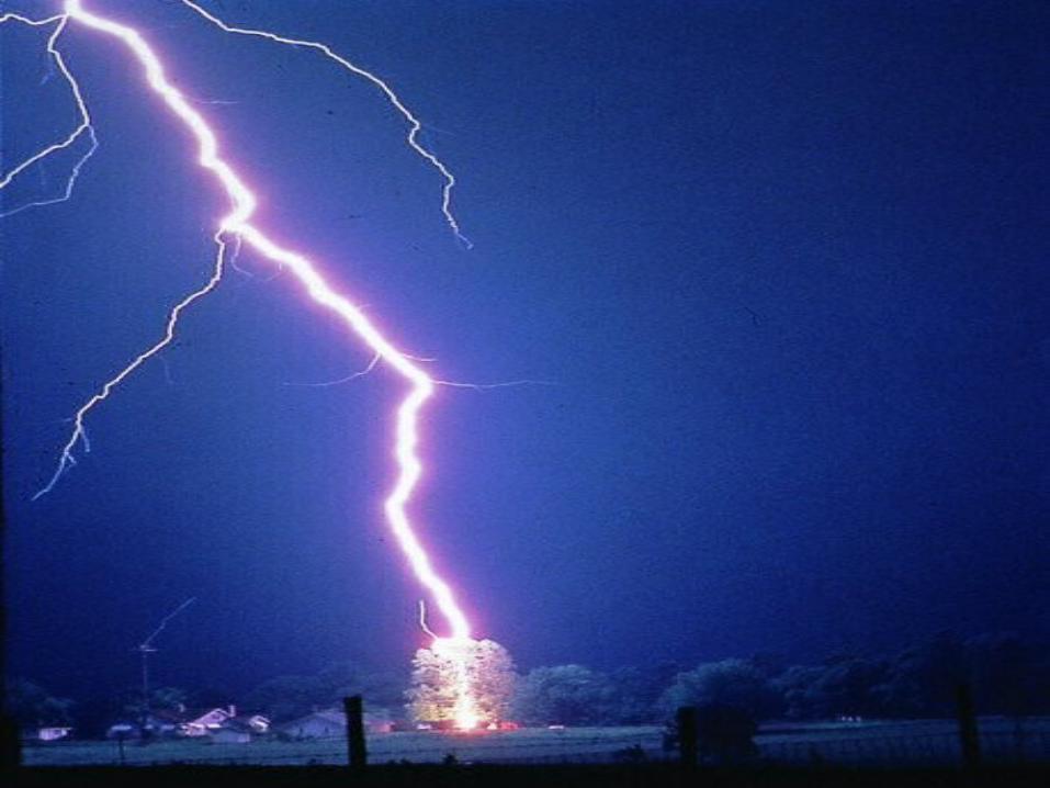
Plasma: the 4th state of the matterPlasma: the 4th state of the matter
On earth we live upon an island of "ordinary" matter. The different states of matter generally found on earth are solid, liquid, and gas. We have learned to work, play, and rest using these familiar states of matter. Sir William Crookes, an English physicist, identified a fourth state of matter, now called plasma, in 1879. Plasma is by far the most common form of matter. Plasma in the stars and in the tenuous space between them makes up over 99% of the visible universe and perhaps most of that which is not visible.
Natural plasma Man-made plasmaSources: http://www.plasmas.org/rot-plasmas.htm http://www.4thstate.com/publications/21stCentury.htm
39Technion- Microelectronic Processing – Joseph Salzman – Fall 2006
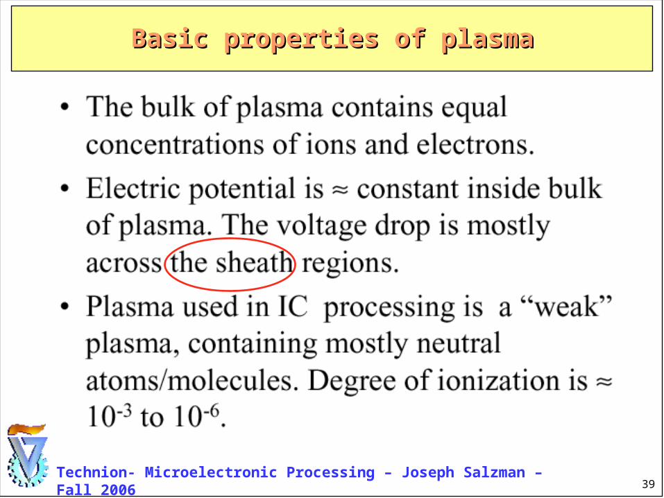
Basic properties of plasmaBasic properties of plasma
40Technion- Microelectronic Processing – Joseph Salzman – Fall 2006
41Technion- Microelectronic Processing – Joseph Salzman – Fall 2006
42Technion- Microelectronic Processing – Joseph Salzman – Fall 2006
43Technion- Microelectronic Processing – Joseph Salzman – Fall 2006
44Technion- Microelectronic Processing – Joseph Salzman – Fall 2006
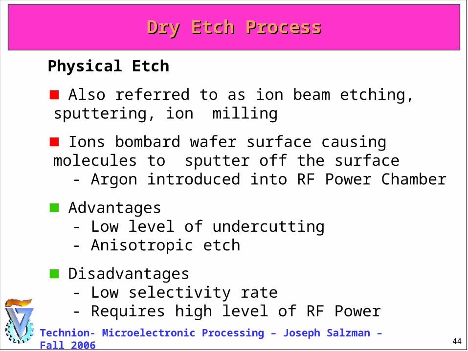
Physical Etch
Also referred to as ion beam etching, sputtering, ion .milling
Ions bombard wafer surface causing molecules to .sputter off the surface - Argon introduced into RF Power Chamber
Advantages - Low level of undercutting - Anisotropic etch
Disadvantages - Low selectivity rate - Requires high level of RF Power
Dry Etch ProcessDry Etch Process
45Technion- Microelectronic Processing – Joseph Salzman – Fall 2006
Sputter etchingSputter etching
In this process all of the electrical energy, usually RF, is applied to the substrate.Physically bombard the films to be etched with energized chemically inert ions or atoms.Material is removed by ion bombardment of the substrate. This process is most often used to pre-clean substrates prior to deposition.Glow discharge is used to energize chemically inert ions or atoms (e.g., Ar)
Highly anisotropic etching
– Damage to underlying material => may change device properties
– Rarely used in VLSI
46Technion- Microelectronic Processing – Joseph Salzman – Fall 2006
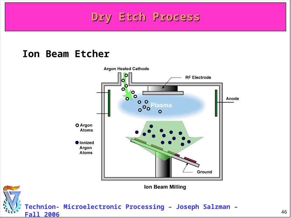
Ion Beam Etcher
Dry Etch ProcessDry Etch Process
47Technion- Microelectronic Processing – Joseph Salzman – Fall 2006
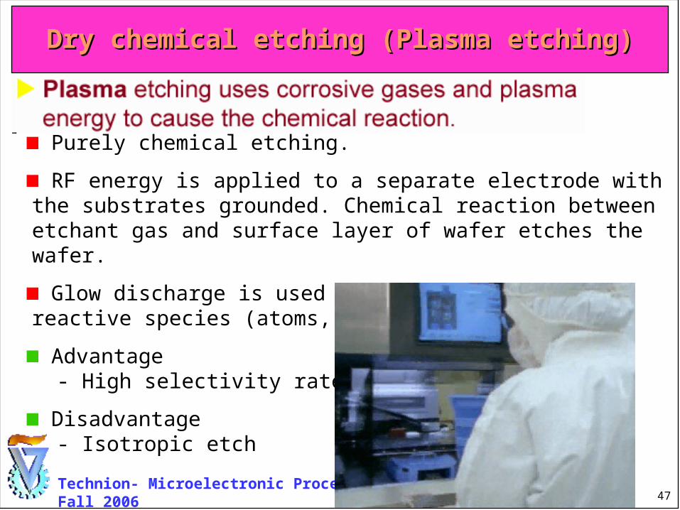
Dry chemical etching (Plasma etching)Dry chemical etching (Plasma etching)
Purely chemical etching.
RF energy is applied to a separate electrode with the substrates grounded. Chemical reaction between etchant gas and surface layer of wafer etches the wafer.
Glow discharge is used to produce chemically reactive species (atoms, radicals, or ions).
Advantage - High selectivity rate
Disadvantage - Isotropic etch
48Technion- Microelectronic Processing – Joseph Salzman – Fall 2006
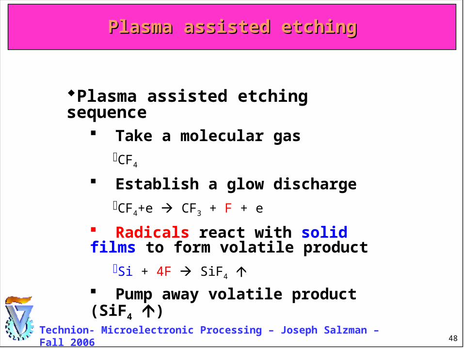
Plasma assisted etchingPlasma assisted etching
Plasma assisted etching sequence Take a molecular gas
CF4
Establish a glow dischargeCF4+e CF3 + F + e
Radicals react with solid films to form volatile product
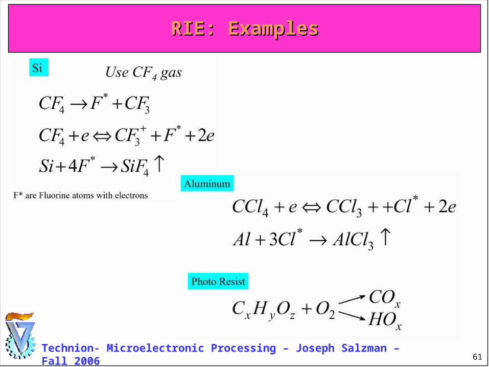
Si + 4F SiF4
Pump away volatile product (SiF4 )
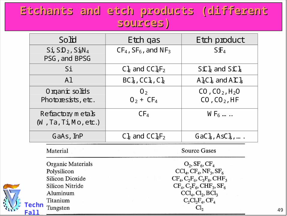
49Technion- Microelectronic Processing – Joseph Salzman – Fall 2006
Etchants and etch products (different Etchants and etch products (different sources)sources)
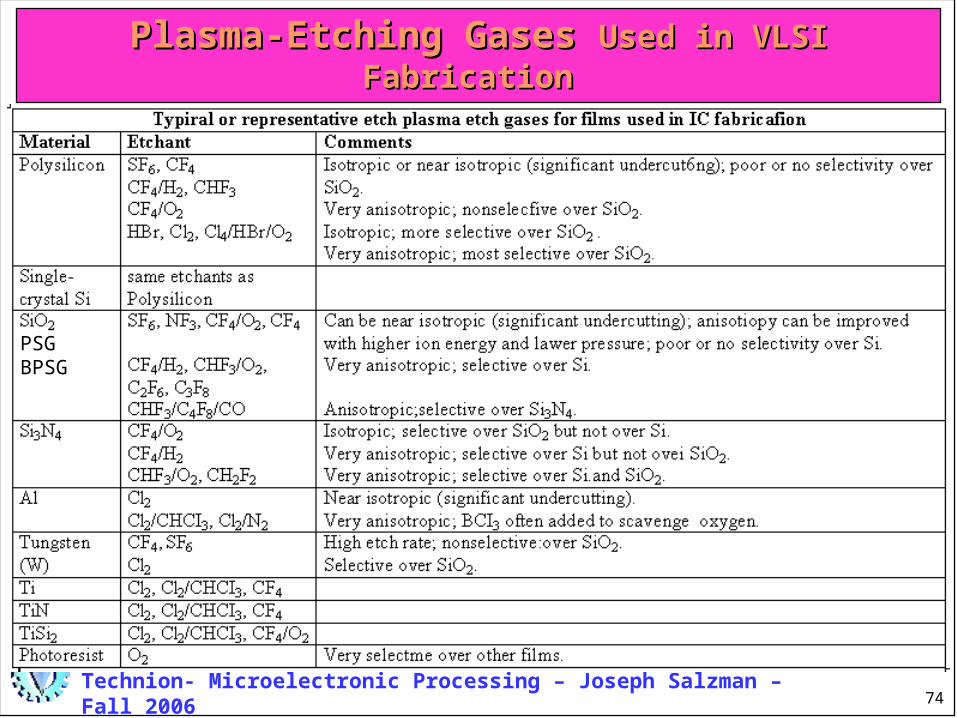
Solid Etch gas Etch productSi, SiO2, Si3N4
PSG, and BPSGCF4, SF6, and NF3 SiF4
Si Cl2 and CCl2F2 SiCl2 and SiCl4Al BCl3, CCl4, Cl2 Al2Cl6 and AlCl3
Organic solidsPhotoresists, etc.
O2
O2 + CF4
CO, CO2, H2OCO, CO2, HF
Refractory metals(W, Ta, Ti, Mo, etc.)
CF4 WF6 …..
GaAs, InP Cl2 and CCl2F2 GaCl3, AsCl5, ….
50Technion- Microelectronic Processing – Joseph Salzman – Fall 2006
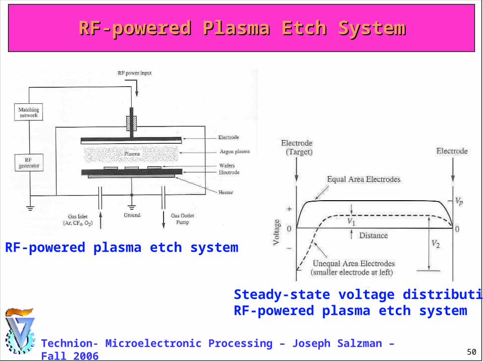
RF-powered Plasma Etch SystemRF-powered Plasma Etch System
RF-powered plasma etch system
Steady-state voltage distribution inRF-powered plasma etch system
51Technion- Microelectronic Processing – Joseph Salzman – Fall 2006
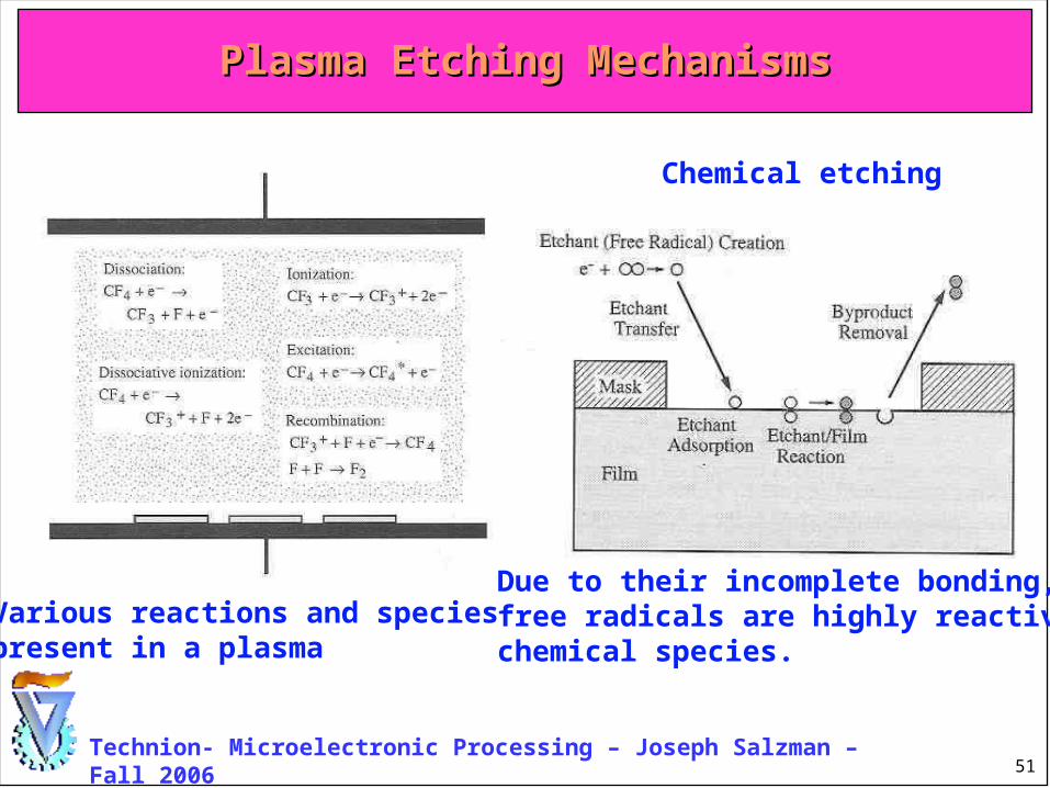
Plasma Etching MechanismsPlasma Etching Mechanisms
Chemical etching
Various reactions and speciespresent in a plasma
Due to their incomplete bonding, free radicals are highly reactive chemical species.
52Technion- Microelectronic Processing – Joseph Salzman – Fall 2006
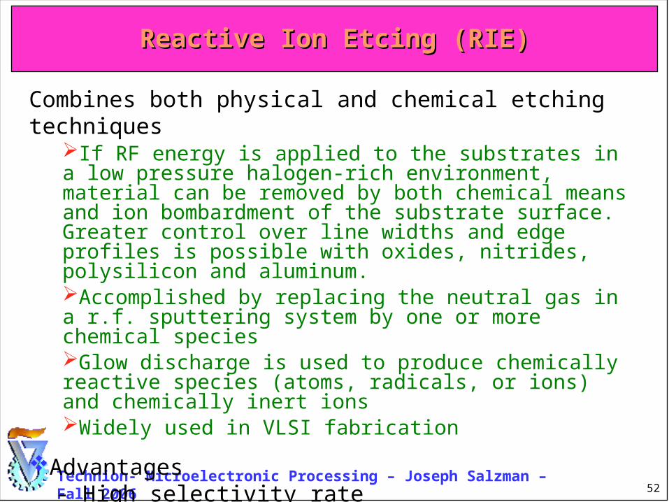
Combines both physical and chemical etching techniquesIf RF energy is applied to the substrates in a low pressure halogen-rich environment, material can be removed by both chemical means and ion bombardment of the substrate surface. Greater control over line widths and edge profiles is possible with oxides, nitrides, polysilicon and aluminum.Accomplished by replacing the neutral gas in a r.f. sputtering system by one or more chemical speciesGlow discharge is used to produce chemically reactive species (atoms, radicals, or ions) and chemically inert ionsWidely used in VLSI fabrication
Advantages - High selectivity rate - Anisotropic
Reactive Ion Etcing (RIE)Reactive Ion Etcing (RIE)
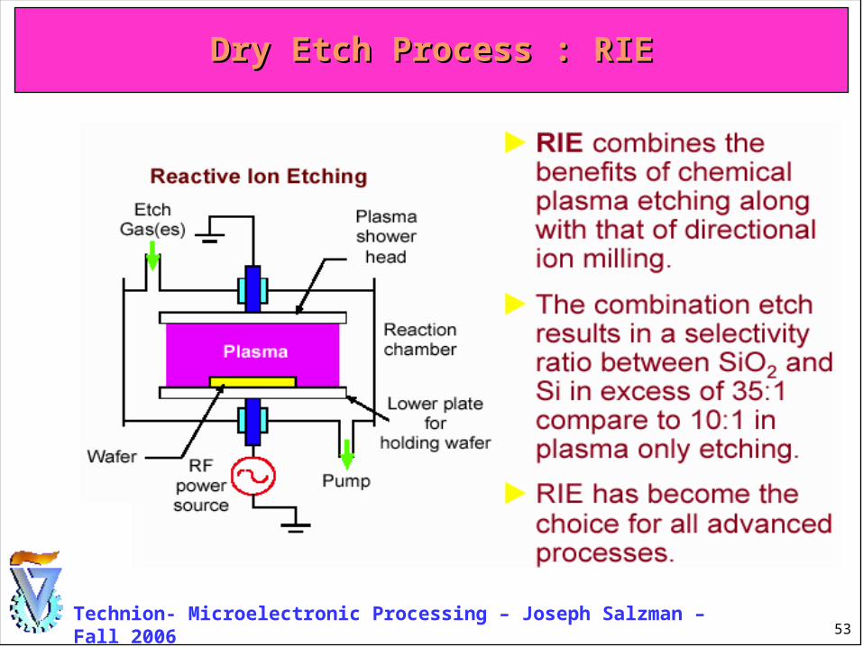
53Technion- Microelectronic Processing – Joseph Salzman – Fall 2006
Dry Etch Process : RIEDry Etch Process : RIE
54Technion- Microelectronic Processing – Joseph Salzman – Fall 2006
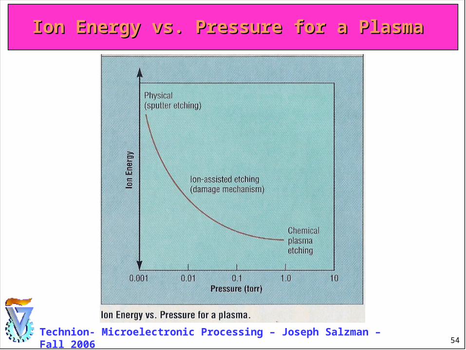
Ion Energy vs. Pressure for a Plasma Ion Energy vs. Pressure for a Plasma
55Technion- Microelectronic Processing – Joseph Salzman – Fall 2006
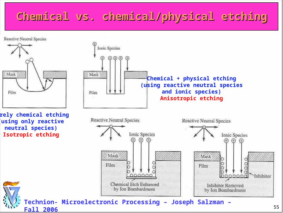
Chemical vs. chemical/physical etchingChemical vs. chemical/physical etching
Purely chemical etching(using only reactive
neutral species)Isotropic etching
Chemical + physical etching(using reactive neutral species
and ionic species)Anisotropic etching
56Technion- Microelectronic Processing – Joseph Salzman – Fall 2006
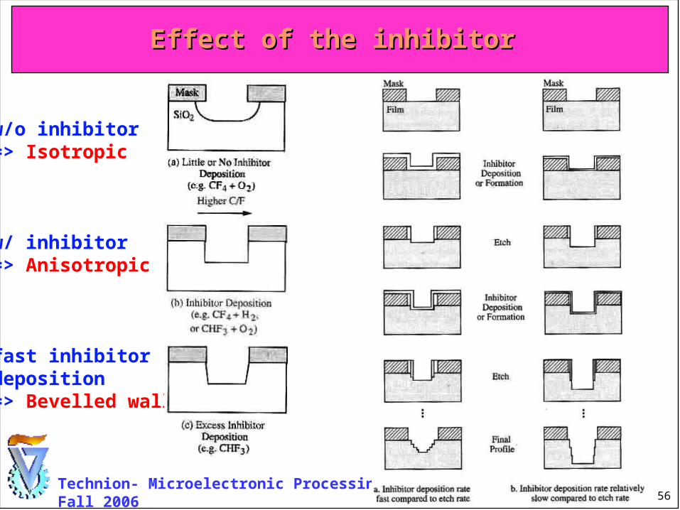
Effect of the inhibitorEffect of the inhibitor
w/o inhibitor=> Isotropic
w/ inhibitor=> Anisotropic
fast inhibitordeposition=> Bevelled walls
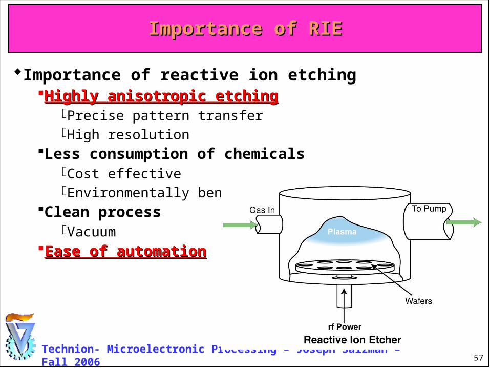
57Technion- Microelectronic Processing – Joseph Salzman – Fall 2006
Importance of reactive ion etchingHighly anisotropic etchingHighly anisotropic etching
Precise pattern transferHigh resolution
Less consumption of chemicalsCost effectiveEnvironmentally benign
Clean processVacuum
Ease of automationEase of automation
Importance of RIEImportance of RIE
58Technion- Microelectronic Processing – Joseph Salzman – Fall 2006
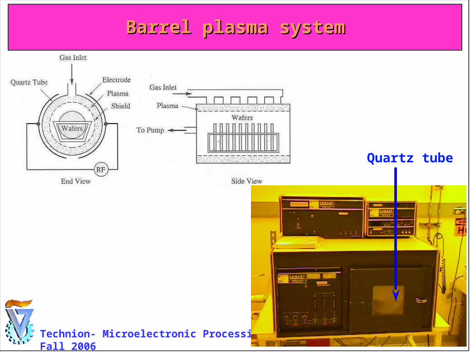
Barrel plasma systemBarrel plasma system
Quartz tube
59Technion- Microelectronic Processing – Joseph Salzman – Fall 2006
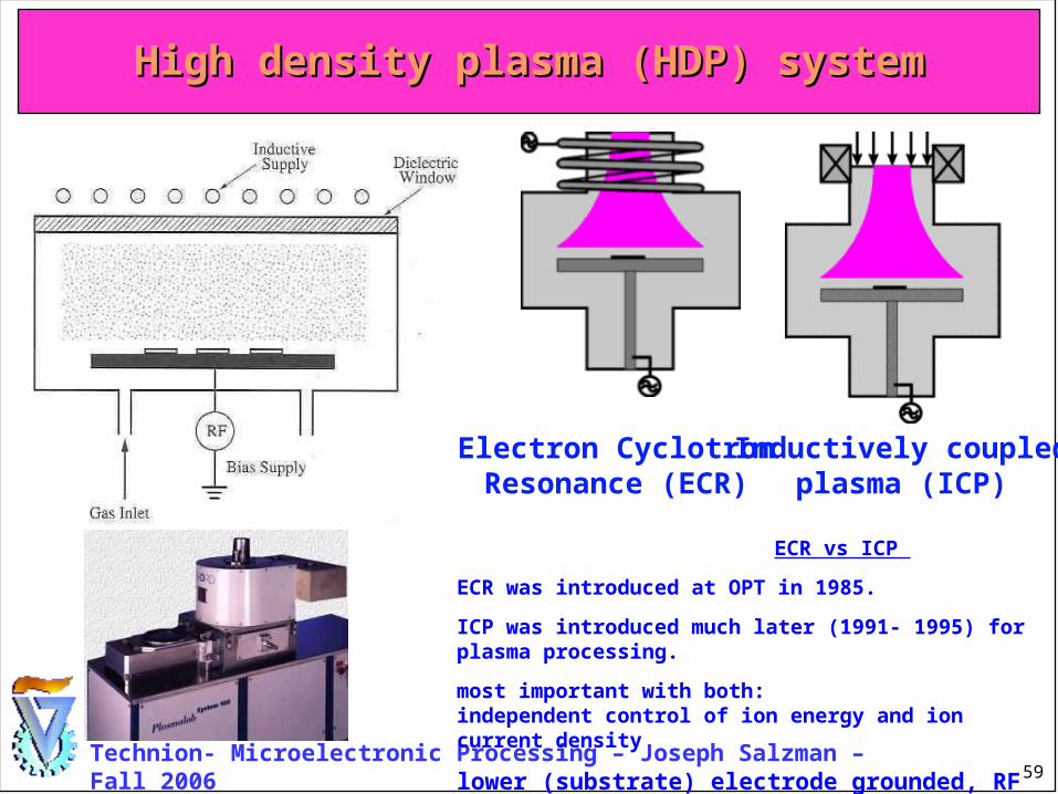
High density plasma (HDP) systemHigh density plasma (HDP) system
ECR vs ICP
ECR was introduced at OPT in 1985.
ICP was introduced much later (1991- 1995) for plasma processing.
most important with both: independent control of ion energy and ion current density
lower (substrate) electrode grounded, RF driving opt.
Electron CyclotronResonance (ECR)
Inductively coupledplasma (ICP)
60Technion- Microelectronic Processing – Joseph Salzman – Fall 2006
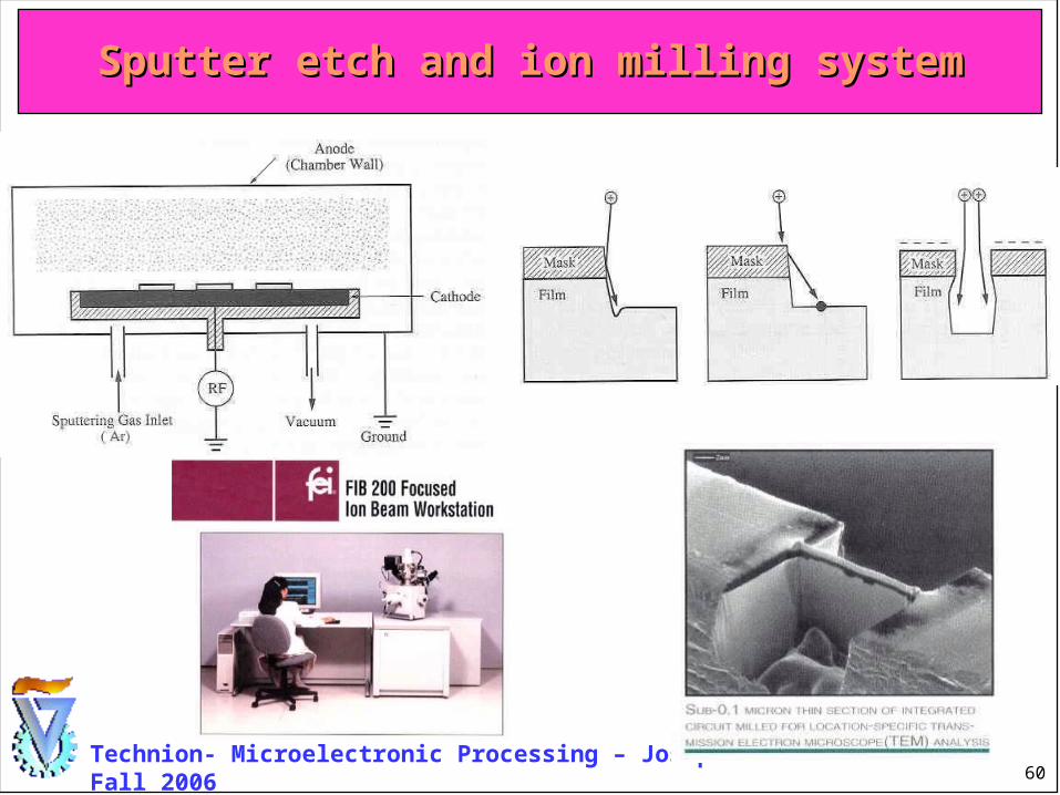
Sputter etch and ion milling systemSputter etch and ion milling system
61Technion- Microelectronic Processing – Joseph Salzman – Fall 2006
RIE: ExamplesRIE: Examples
62Technion- Microelectronic Processing – Joseph Salzman – Fall 2006
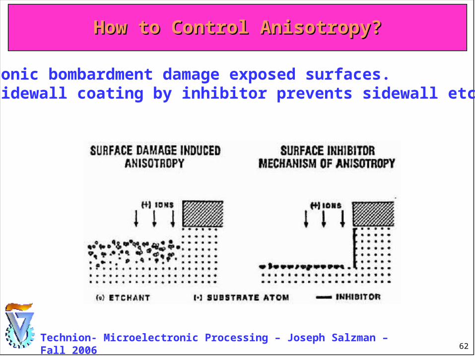
How to Control Anisotropy?How to Control Anisotropy?
1) Ionic bombardment damage exposed surfaces.2) Sidewall coating by inhibitor prevents sidewall etching.
63Technion- Microelectronic Processing – Joseph Salzman – Fall 2006
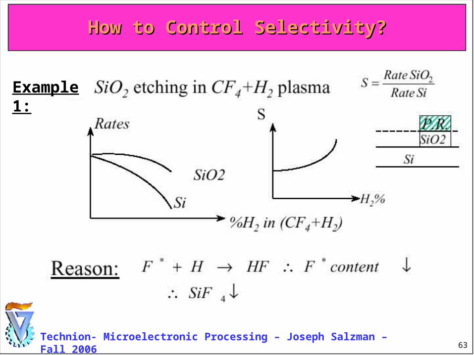
How to Control Selectivity?How to Control Selectivity?
Example 1:
64Technion- Microelectronic Processing – Joseph Salzman – Fall 2006
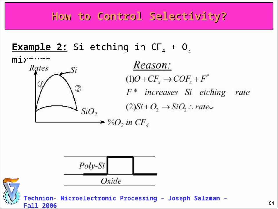
How to Control Selectivity?How to Control Selectivity?
Example 2: Si etching in CF4 + O2 mixture.
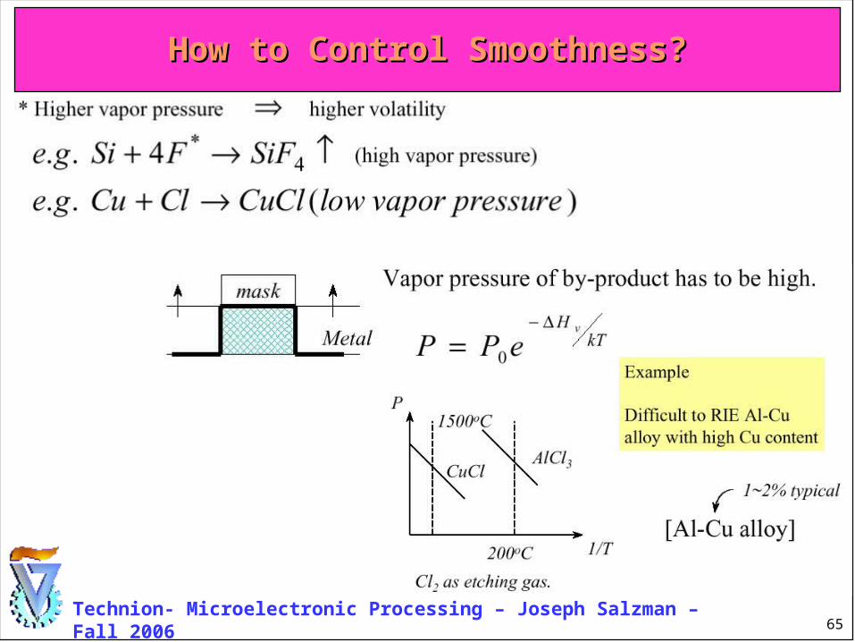
65Technion- Microelectronic Processing – Joseph Salzman – Fall 2006
How to Control Smoothness?How to Control Smoothness?
66Technion- Microelectronic Processing – Joseph Salzman – Fall 2006
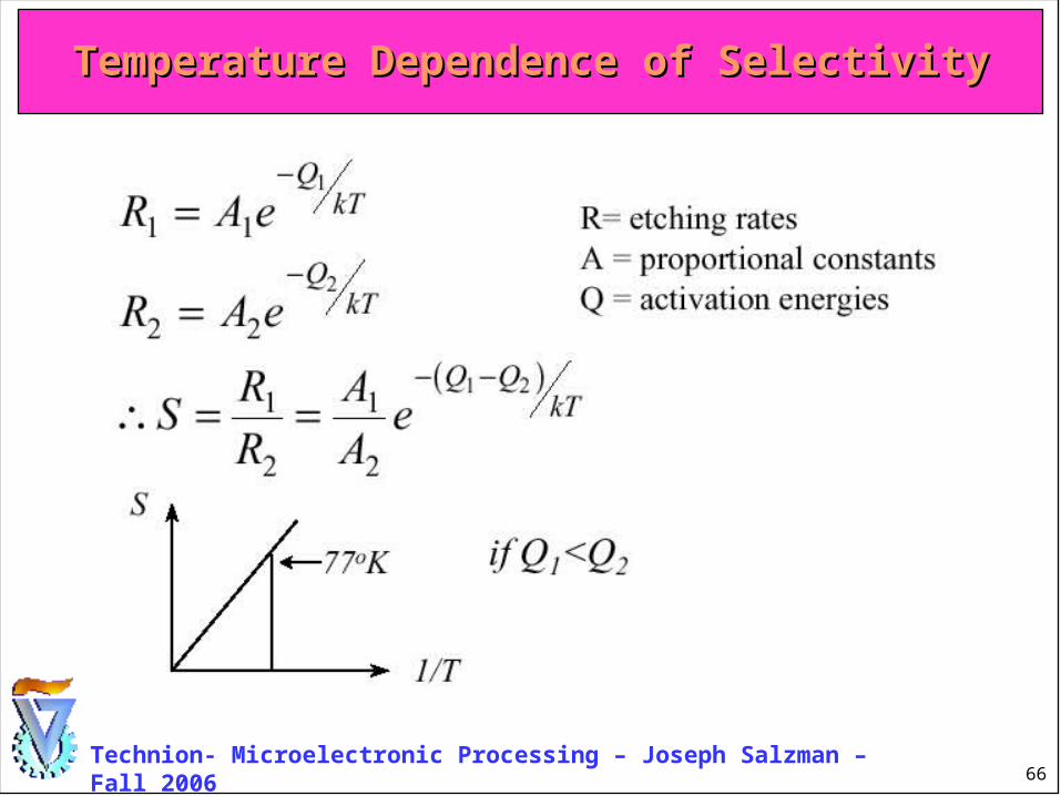
Temperature Dependence of SelectivityTemperature Dependence of Selectivity
67Technion- Microelectronic Processing – Joseph Salzman – Fall 2006
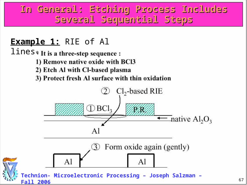
In General: Etching Process Includes In General: Etching Process Includes Several Sequential StepsSeveral Sequential Steps
Example 1: RIE of Al lines.
68Technion- Microelectronic Processing – Joseph Salzman – Fall 2006
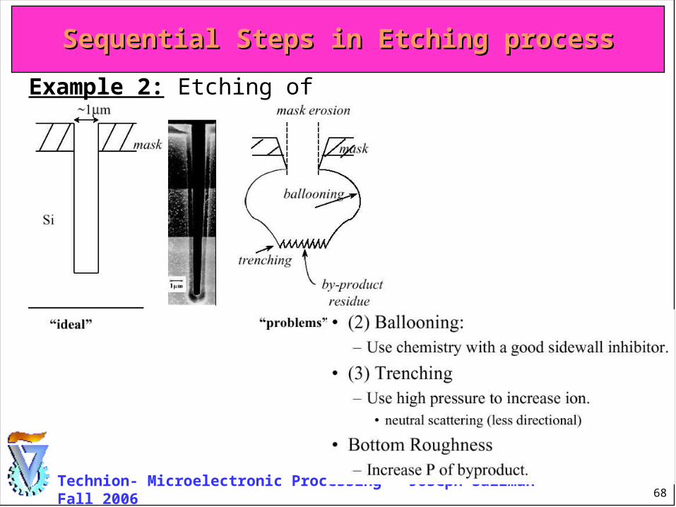
Sequential Steps in Etching processSequential Steps in Etching process
Example 2: Etching of deep trenches.
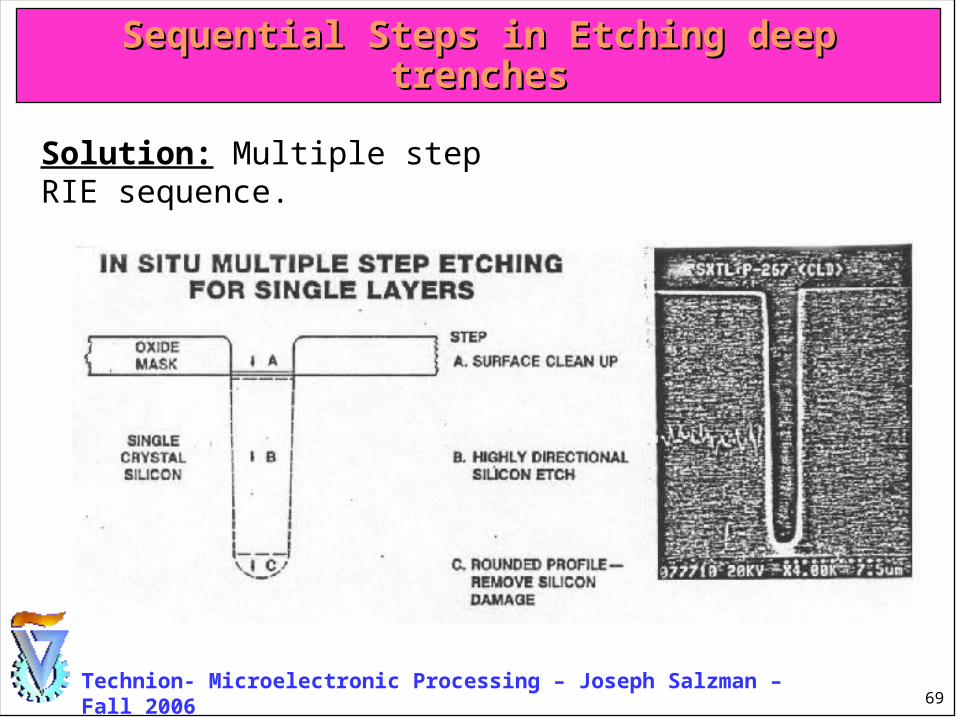
69Technion- Microelectronic Processing – Joseph Salzman – Fall 2006
Sequential Steps in Etching deep trenchesSequential Steps in Etching deep trenches
Solution: Multiple step RIE sequence.
70Technion- Microelectronic Processing – Joseph Salzman – Fall 2006
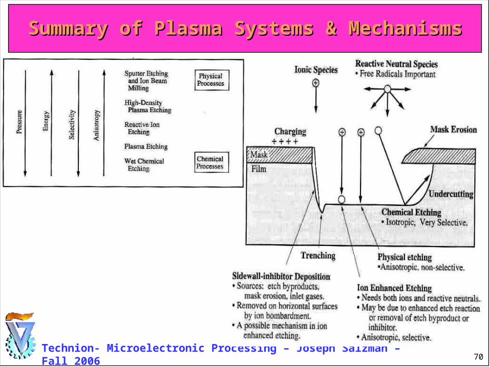
Summary of Plasma Systems & Summary of Plasma Systems & MechanismsMechanisms
71Technion- Microelectronic Processing – Joseph Salzman – Fall 2006
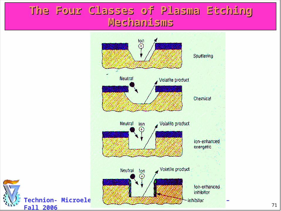
The Four Classes of Plasma Etching The Four Classes of Plasma Etching MechanismsMechanisms
72Technion- Microelectronic Processing – Joseph Salzman – Fall 2006
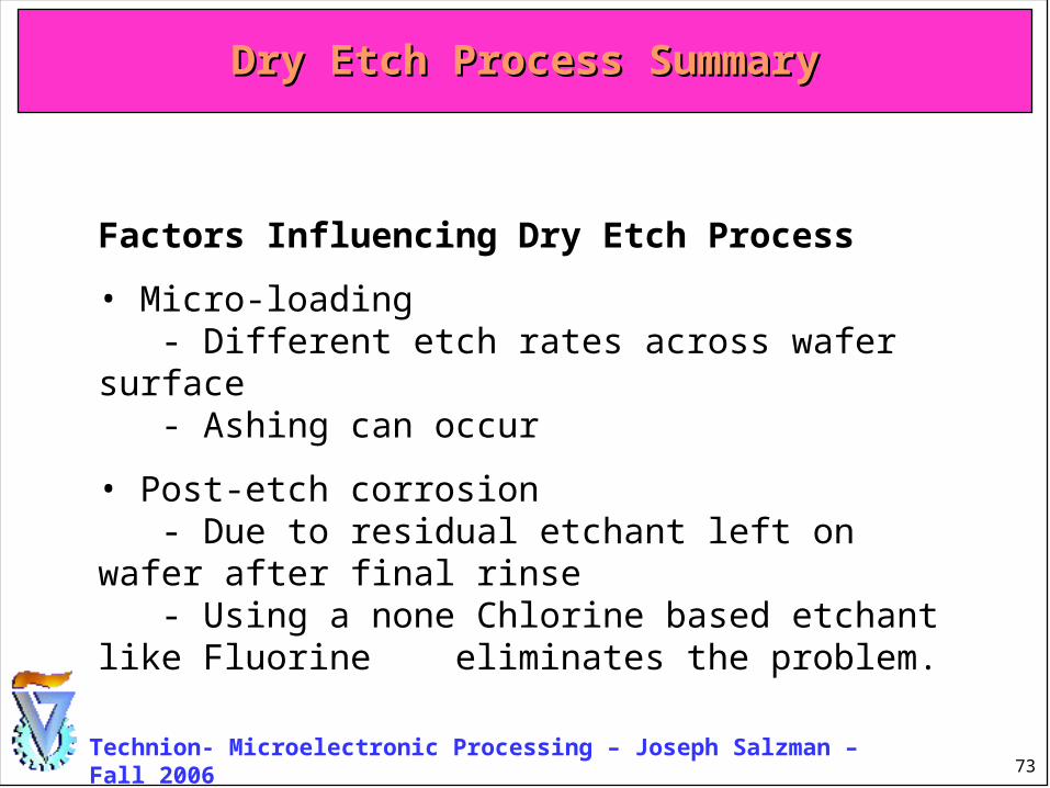
Factors Influencing Dry Etch Process
• Etch rate - RF Power level - Gas formula - Etch Temperature
• Pressure - Extremely high pressure results in an isotropic etch - Low pressure with high energy can damage wafer
Dry Etch Process SummaryDry Etch Process Summary
73Technion- Microelectronic Processing – Joseph Salzman – Fall 2006
Factors Influencing Dry Etch Process
• Micro-loading - Different etch rates across wafer surface - Ashing can occur
• Post-etch corrosion - Due to residual etchant left on wafer after final rinse - Using a none Chlorine based etchant like Fluorine …..eliminates the problem.
Dry Etch Process SummaryDry Etch Process Summary
74Technion- Microelectronic Processing – Joseph Salzman – Fall 2006
Plasma-Etching Gases Plasma-Etching Gases Used in VLSI Used in VLSI FabricationFabrication
PSGBPSG
75Technion- Microelectronic Processing – Joseph Salzman – Fall 2006
Resist Stripping
• Removes residual resist after etch process
• Wet stripping - For use on wafers that have not been plasma …. …..etched - For non-metallic surfaces an acid solvent is used - For metallic surfaces an organic solvent is used
• Plasma Stripping - For use on wafers that have been etched by plasma - Uses oxygen as stripping plasma to remove …..photoresist
Wafer CleaningWafer Cleaning
76Technion- Microelectronic Processing – Joseph Salzman – Fall 2006
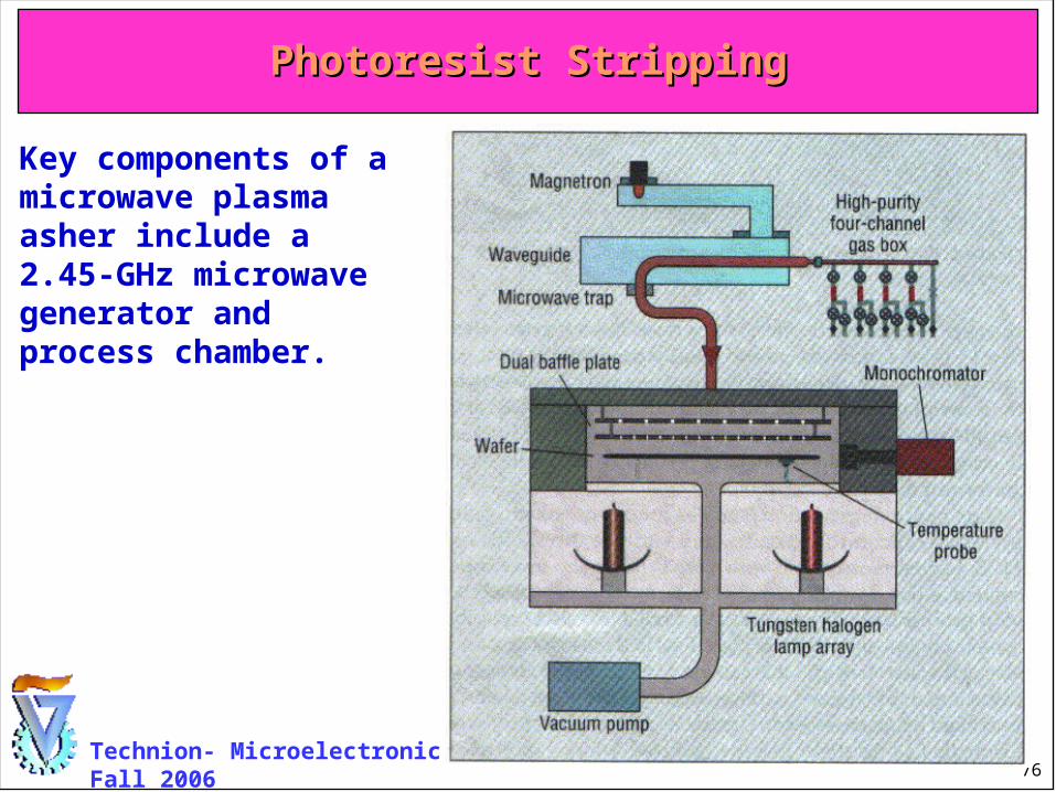
Photoresist StrippingPhotoresist Stripping
Key components of a microwave plasma asher include a 2.45-GHz microwave generator and process chamber.
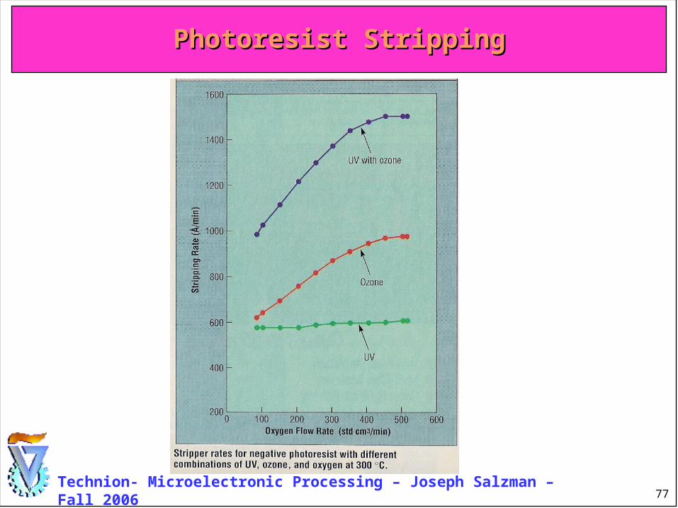
77Technion- Microelectronic Processing – Joseph Salzman – Fall 2006
Photoresist StrippingPhotoresist Stripping
78Technion- Microelectronic Processing – Joseph Salzman – Fall 2006
Etch check
Final check
Critical dimension measurement
Wafer Inspection and MetrologyWafer Inspection and Metrology