Embed Size (px)
Citation preview
1
Lecture 10a: Digital Signal Processors:A TI Architectural History
Collated by: Professor Kurt KeutzerComputer Science 252, Spring 2000
With contributions from:Dr. Brock Barton, Clark Hise TI; Dr. Surendar S. Magar, Berkeley Concept Research Corporation
2
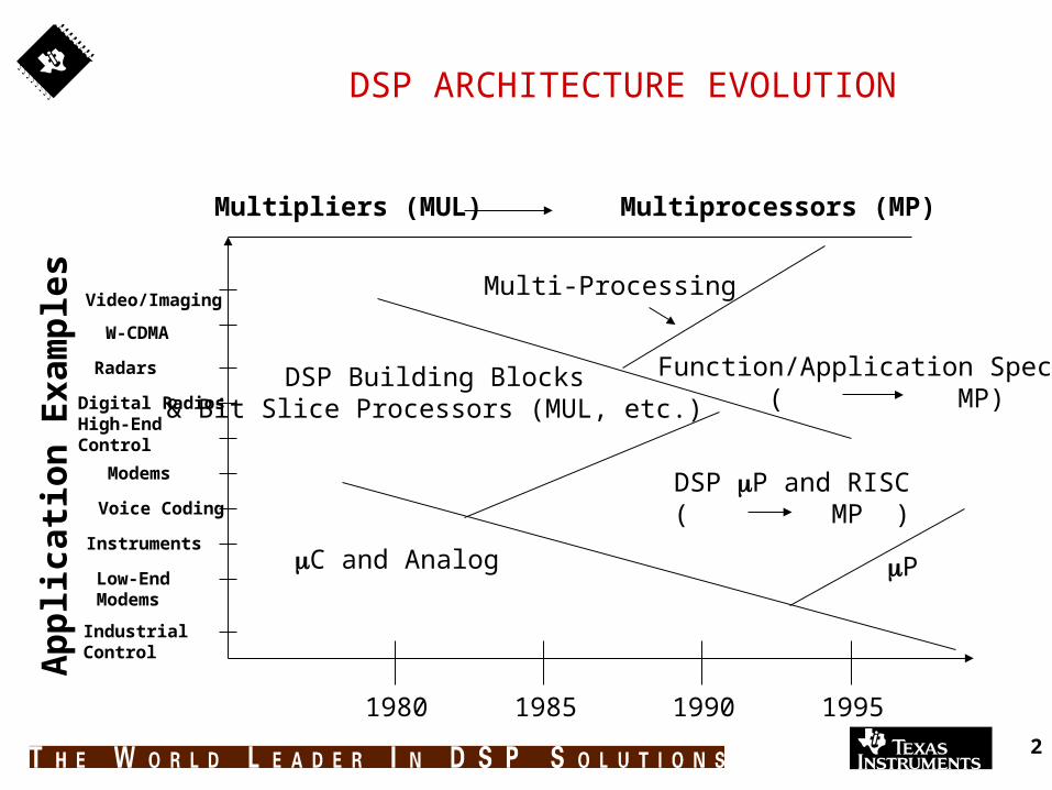
DSP ARCHITECTURE EVOLUTION
Video/Imaging
W-CDMA
Radars
Digital RadiosHigh-EndControl
Modems
Voice Coding
Instruments
Low-EndModems
IndustrialControl
Multi-Processing
DSP Building Blocks& Bit Slice Processors (MUL, etc.)
C and Analog
DSP P and RISC( MP )
Function/Application Specific( MP)
Ap
pli
cati
on E
xam
ple
s
1980 1985 1990 1995
Multipliers (MUL) Multiprocessors (MP)
P
3
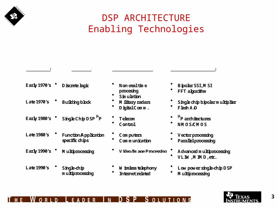
DSP ARCHITECTUREEnabling Technologies
Time Frame Approach Primary Application Enabling Technologies
Early 1970’s Discrete logic Non-real timeprocesing
Simulation
Bipolar SSI, MSI FFT algorithm
Late 1970’s Building block Military radars Digital Comm.
Single chip bipolar multiplier Flash A/D
Early 1980’s Single Chip DSP P Telecom Control
P architectures NMOS/CMOS
Late 1980’s Function/Applicationspecific chips
Computers Communication
Vector processing Parallel processing
Early 1990’s Multiprocessing Video/Image Processing Advanced multiprocessing VLIW, MIMD, etc.
Late 1990’s Single-chipmultiprocessing
Wireless telephony Internet related
Low power single-chip DSP Multiprocessing
4
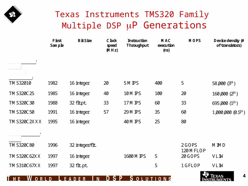
Texas Instruments TMS320 Family Multiple DSP P Generations
FirstSample
Bit Size Clockspeed(MHz)
InstructionThroughput
MACexecution
(ns)
MOPS Device density (#of transistors)
Uniprocessor Based (Harvard Architecture) TMS32010 1982 16 integer 20 5 MIPS 400 5 58,000 (3)
TMS320C25 1985 16 integer 40 10 MIPS 100 20 160,000 (2)
TMS320C30 1988 32 flt.pt. 33 17 MIPS 60 33 695,000 (1)
TMS320C50 1991 16 integer 57 29 MIPS 35 60 1,000,000 (0.5)
TMS320C2XXX 1995 16 integer 40 MIPS 25 80
Multiprocessor Based TMS320C80 1996 32 integer/flt. 2 GOPS
120 MFLOPMIMD
TMS320C62XX 1997 16 integer 1600 MIPS 5 20 GOPS VLIW
TMS310C67XX 1997 32 flt. pt. 5 1 GFLOP VLIW
5
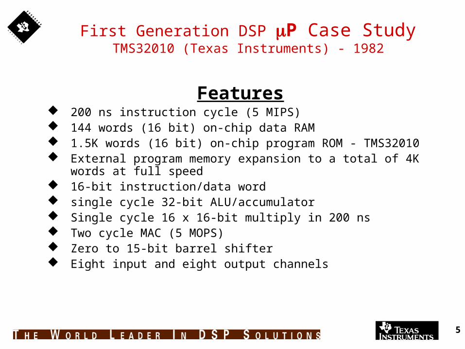
First Generation DSP P Case StudyTMS32010 (Texas Instruments) - 1982
Features 200 ns instruction cycle (5 MIPS) 144 words (16 bit) on-chip data RAM 1.5K words (16 bit) on-chip program ROM - TMS32010 External program memory expansion to a total of 4K words at full
speed 16-bit instruction/data word single cycle 32-bit ALU/accumulator Single cycle 16 x 16-bit multiply in 200 ns Two cycle MAC (5 MOPS) Zero to 15-bit barrel shifter Eight input and eight output channels

6
TMS32010 BLOCK DIAGRAM

7
TMS32010 Program Memory Maps
Address
0
1
2
Microcomputer Mode
16-bit word
Reset 1st Word
Reset 2nd Word
Interrupt
InternalMemory
Space
InternalMemory
Space ReservedFor Testing
ExternalMemory
Space
Reset 1st Word
Reset 2nd Word
Interrupt
0
1
2
Microprocessor Mode
16-bit word
External Memory
Space1525
1536
4095 4095

8
Digital FIR Filter Implementation(Uniprocessor-Circular Buffer)
X
Start
End
2nd. Cycle1st. Cycle
End
Start eachTime here
a n-1 a n-2 a 1 a 0
a n-1a 0
Replacestarting
valuewith new
value
X0
X1
X2
X3
X4
X5
Xn-1
Start
Acc
+

9
TMS32010 FIR FILTER PROGRAMIndirect Addressing (Smaller Program Space)
Y(n) = x[n-(N-1)] . h(N-1) + x[n-(N-2)] . h(N-2) +…+ x(n) . h(0)
For N=50, Indirect Addressing t=42 s (23.8 KHz)For N=50, Direct Addressing t=21.6 s (40.2 KHz)
10
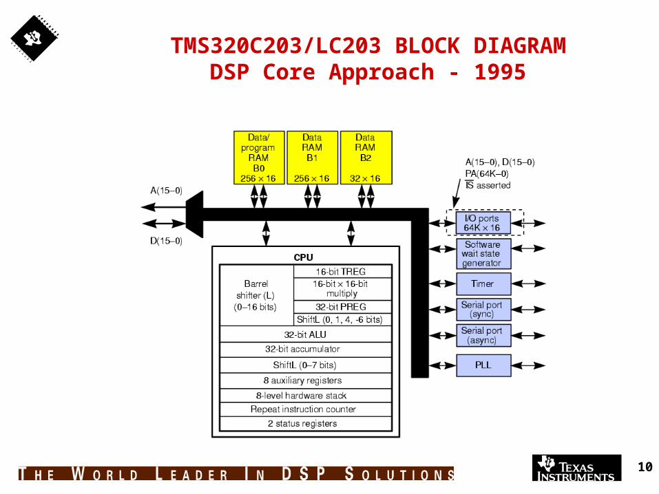
TMS320C203/LC203 BLOCK DIAGRAMDSP Core Approach - 1995
11
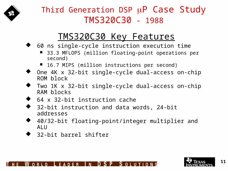
Third Generation DSP P Case StudyTMS320C30 - 1988
TMS320C30 Key Features 60 ns single-cycle instruction execution time
33.3 MFLOPS (million floating-point operations per second) 16.7 MIPS (million instructions per second)
One 4K x 32-bit single-cycle dual-access on-chip ROM block Two 1K x 32-bit single-cycle dual-access on-chip RAM blocks 64 x 32-bit instruction cache 32-bit instruction and data words, 24-bit addresses 40/32-bit floating-point/integer multiplier and ALU 32-bit barrel shifter
12
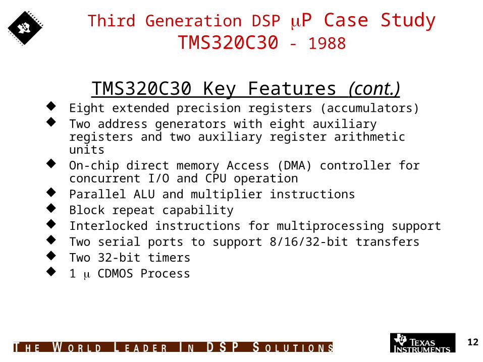
Third Generation DSP P Case StudyTMS320C30 - 1988
TMS320C30 Key Features (cont.) Eight extended precision registers (accumulators) Two address generators with eight auxiliary registers and two auxiliary
register arithmetic units On-chip direct memory Access (DMA) controller for concurrent I/O and
CPU operation Parallel ALU and multiplier instructions Block repeat capability Interlocked instructions for multiprocessing support Two serial ports to support 8/16/32-bit transfers Two 32-bit timers 1 CDMOS Process

13
TMS320C30 BLOCK DIAGRAM

14
TMS320C3x CPU BLOCK DIAGRAM
15
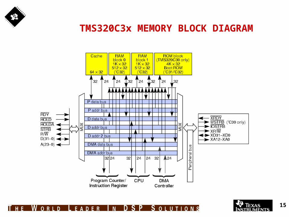
TMS320C3x MEMORY BLOCK DIAGRAM

16
TMS320C30 Memory Organization
Interrupt locations& reserved (192)
external STRB active
ExternalSTRB Active
Oh
BFhCOh
7FFFFFh800000h
801FFFh802000h
803FFFh804000h
805FFFh806000h
807FFFH80800h
8097FFh809800h
809BFFh809C00h
809FFFh80A00h
0FFFFFFh
Expansion BUS MSTRB Active (8K)Reserved
(8K)
Expansion BusIOSTRB Active (8K)
Reserved(8K)
Peripheral Bus Memory MappedRegisters (Internal) (6K)
RAM Block 0 (1K)(Internal)
RAM Block 1 (1K)(Internal)
ExternalSTRB Active
Oh
BFhCOh
7FFFFFh800000h
801FFFh802000h
803FFFh804000h
805FFFh806000h
807FFFH80800h
8097FFh809800h
809BFFh809C00h
809FFFh80A00h
0FFFFFFh
ExternalSTRB Active
RAM Block 1 (1K)(Internal)
RAM Block 0 (1K)(Internal)
Peripheral Bus Memory MappedRegisters (Internal) (6K)
Reserved(8K)
Expansion BusIOSTRB Active (8K)
Reserved(8K)
Expansion BUS MSTRB Active (8K)
Interrupt locations& reserved (192)
ROM(Internal)0FFFh
1000h
Microprocessor Mode Microcomputer Mode
17
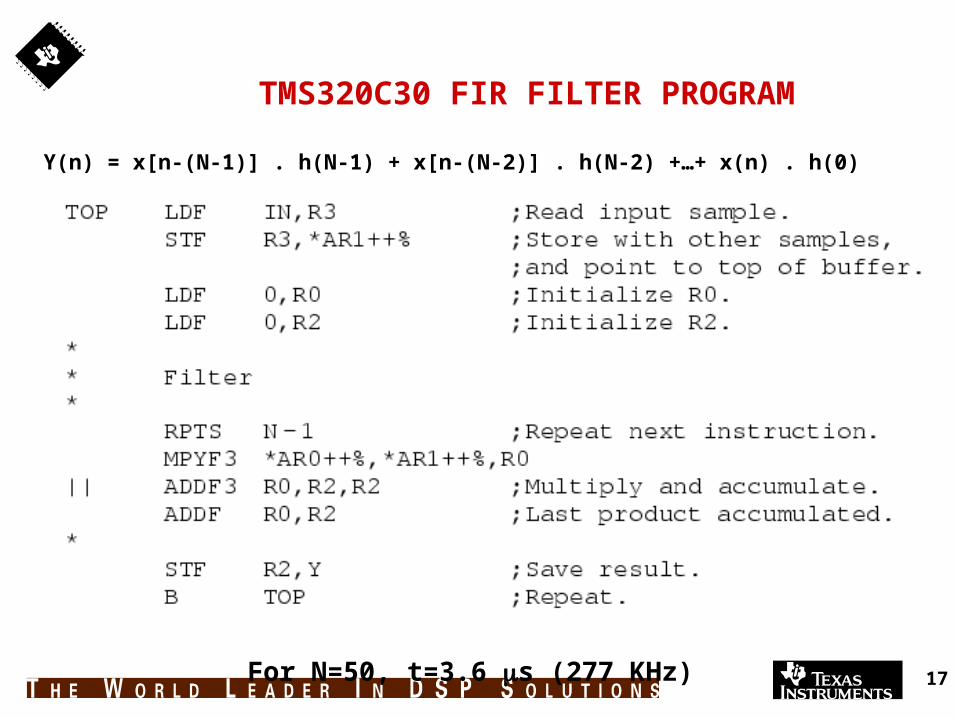
TMS320C30 FIR FILTER PROGRAM
For N=50, t=3.6 s (277 KHz)
Y(n) = x[n-(N-1)] . h(N-1) + x[n-(N-2)] . h(N-2) +…+ x(n) . h(0)

18
‘C54x Architecture

19
TMS320C54x Internal Block Diagram

20
Architecture optimized for DSP#1: CPU designed for efficient DSP processing
MAC unit, 2 Accumulators, Additional Adder, Barrel Shifter
#2: Multiple busses for efficient data and program flow Four busses and large on-chip memory that
result in sustained performance near peak
#3: Highly tuned instruction set for powerful DSP computing Sophisticated instructions that execute in fewer
cycles, with less code and low power demands

21
Key #1: DSP engine
MPY
x a
Y =40 an xn
n = 1*
ADD
y

22
Key #1: MAC Unit
MPY
ADD
MAC *AR2+, *AR3+, A
acc A acc B
Data Coeff PrgmS/US/U
Fractional Mode Bit
ABO
Acc A Temp Acc AData
23
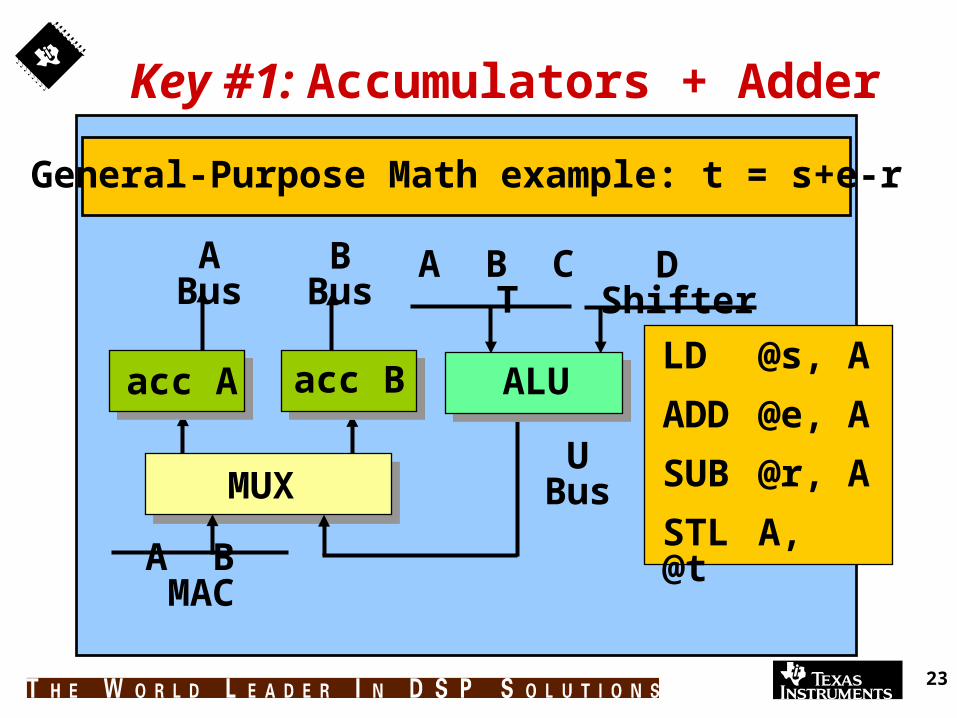
Key #1: Accumulators + Adder
General-Purpose Math example: t = s+e-r
LD @s, A
ADD @e, A
SUB @r, A
STL A, @t
A B C T D ShifterA Bus B Bus
MUX
A B MAC
acc A acc B
U Bus
ALU
24
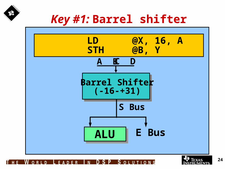
Key #1: Barrel shifter
Barrel Shifter(-16-+31)
S Bus
LD @X, 16, A
C D
ALU E Bus
STH @B, YA B
25
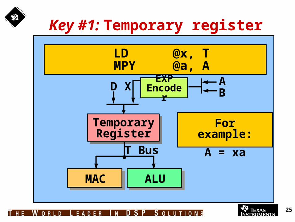
Key #1: Temporary register
TemporaryRegister
ALUMAC
T Bus
D EXPEncoder
ABX
For example:
A = xa
LD @x, TMPY @a, A
26
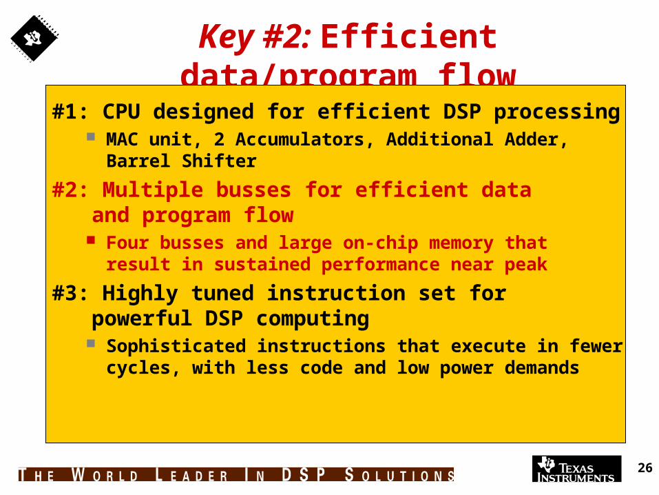
Key #2: Efficient data/program flow
#1: CPU designed for efficient DSP processing MAC unit, 2 Accumulators, Additional Adder,
Barrel Shifter
#2: Multiple busses for efficient data and program flow Four busses and large on-chip memory that
result in sustained performance near peak
#3: Highly tuned instruction set for powerful DSP computing Sophisticated instructions that execute in fewer
cycles, with less code and low power demands
27
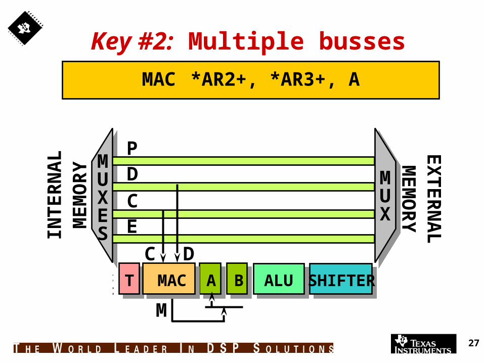
Key #2: Multiple busses
MAC *AR2+, *AR3+, A
CentralArithmeticLogic Unit
EX
TE
RN
AL
ME
MO
RY
MMUUXX
INT
ER
NA
LM
EM
OR
Y MMUUXXEESS
PD
EC
DC
M
ALU SHIFTERBT MAC A

28
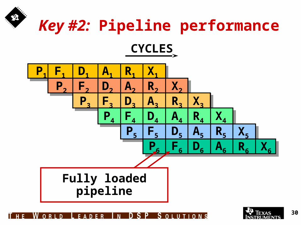
P
Prefetch
F
Fetch
D
Decode
A
Access
R
Read
E
Execute
Key #2: Pipeline
Prefetch: Calculate address of instruction Fetch: Collect instruction Decode: Interpret instruction Access: Collect address of operand Read: Collect operand Execute: Perform operation
29
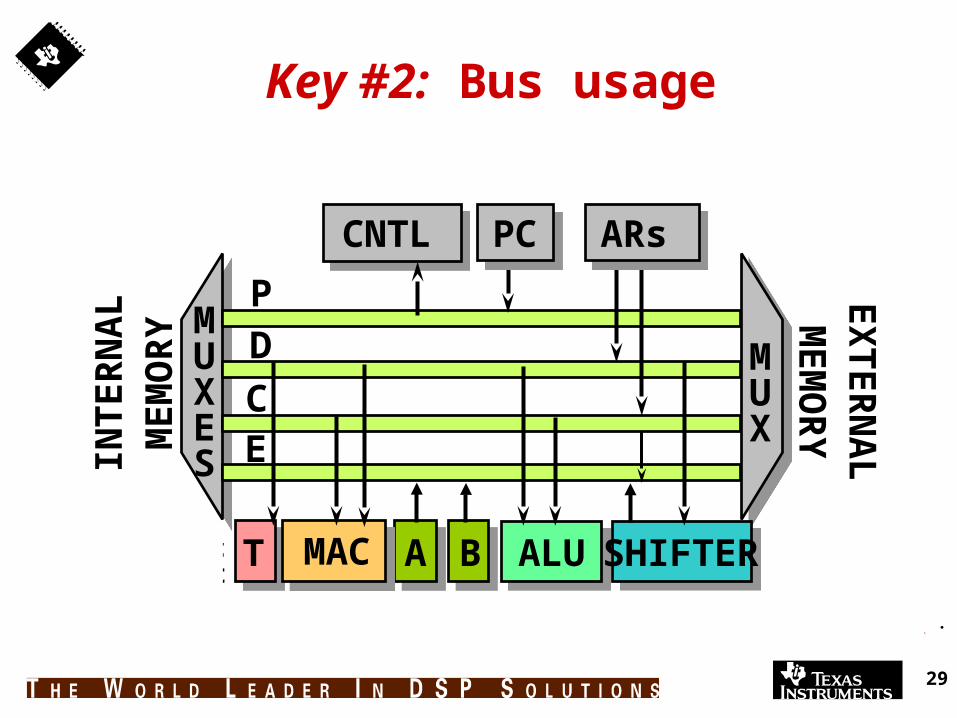
Key #2: Bus usage
CentralArithmeticLogic Unit
EX
TE
RN
AL
ME
MO
RY
MMUUXX
INT
ER
NA
LM
EM
OR
Y MMUUXXEESS
P
ALU SHIFTERBT MAC A
PCCNTL
EC
D
ARs
30
Key #2: Pipeline performance
CYCLES
P1 D1
F2
P3
A1
D2
F3
P4
R1
A2
D3
F4
P5
X1
P6
R2
A3
D4
F5
F6
X2
R3
A4
D5
F1
P2
D6
X3
R4
A5
A6
X4
R5
R6
X5
X6
Fully loaded pipeline
31
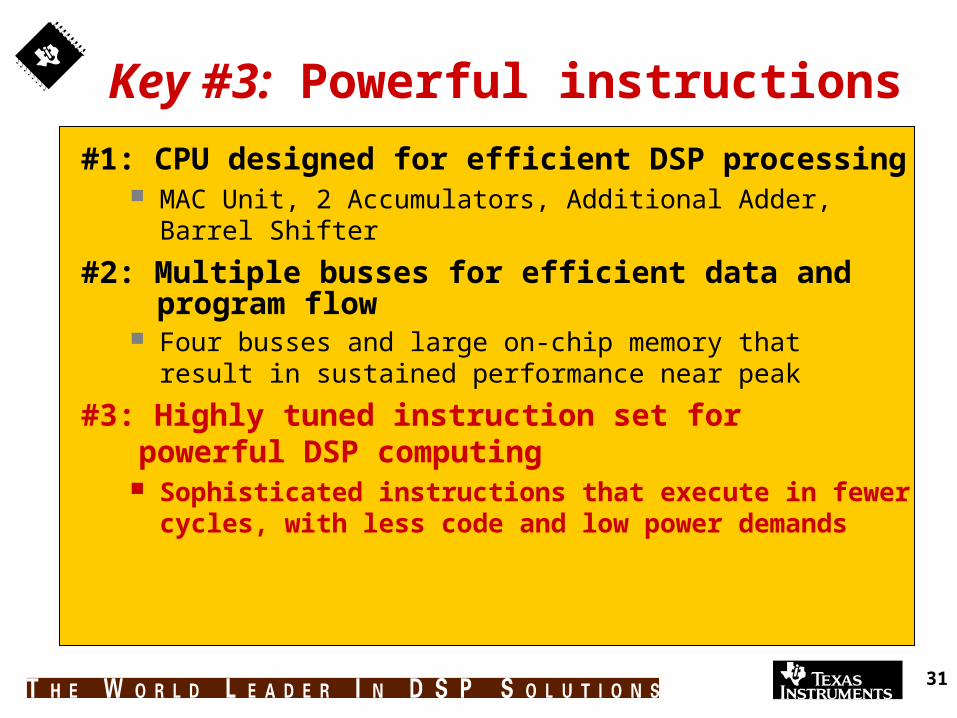
Key #3: Powerful instructions
#1: CPU designed for efficient DSP processing MAC Unit, 2 Accumulators, Additional Adder,
Barrel Shifter
#2: Multiple busses for efficient data and program flow Four busses and large on-chip memory that
result in sustained performance near peak
#3: Highly tuned instruction set for powerful DSP computing Sophisticated instructions that execute in fewer
cycles, with less code and low power demands
32
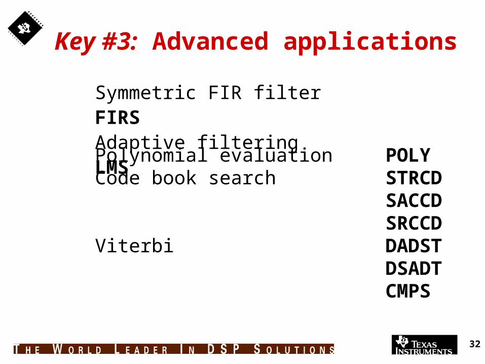
Key #3: Advanced applications
Symmetric FIR filter FIRS Adaptive filtering LMS
Polynomial evaluation POLY Code book search STRCD
SACCD SRCCD
Viterbi DADST DSADT CMPS

33
C62x Architecture

34
TMS320C6201 Revision 2
C6201 CPU Megamodule
Data Path 1
D1M1S1L1
A Register File
Data Path 2
L2S2M2D2
B Register File
Instruction Dispatch
Program Fetch
Interrupts
Control Registers
Control Logic
Emulation
Test
Ext. Memory Interface
4-DMA
Program Cache / Program Memory32-bit address, 256-Bit data512K Bits RAM
Host Port
Interface
2 Timers
2 Multi-channel buffered
serial ports (T1/E1)
Data Memory32-Bit address, 8-, 16-, 32-Bit data
512K Bits RAM
Pwr Dwn
Instruction Decode

35
C6201 Internal Memory Architecture
Separate Internal Program and Data Spaces Program
16K 32-bit instructions (2K Fetch Packets) 256-bit Fetch Width Configurable as either
Direct Mapped Cache, Memory Mapped Program Memory Data
32K x 16 Single Ported Accessible by Both CPU Data Buses 4 x 8K 16-bit Banks
2 Possible Simultaneous Memory Accesses (4 Banks) 4-Way Interleave, Banks and Interleave Minimize Access
Conflicts
36
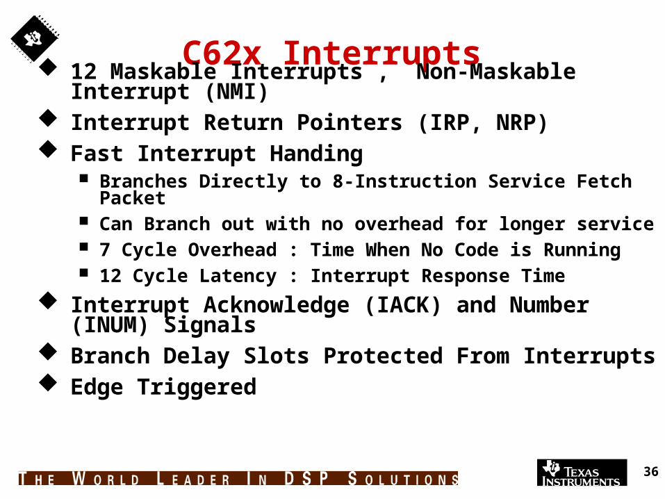
C62x Interrupts 12 Maskable Interrupts , Non-Maskable Interrupt (NMI) Interrupt Return Pointers (IRP, NRP) Fast Interrupt Handing
Branches Directly to 8-Instruction Service Fetch Packet Can Branch out with no overhead for longer service 7 Cycle Overhead : Time When No Code is Running 12 Cycle Latency : Interrupt Response Time
Interrupt Acknowledge (IACK) and Number (INUM) Signals
Branch Delay Slots Protected From Interrupts Edge Triggered

37
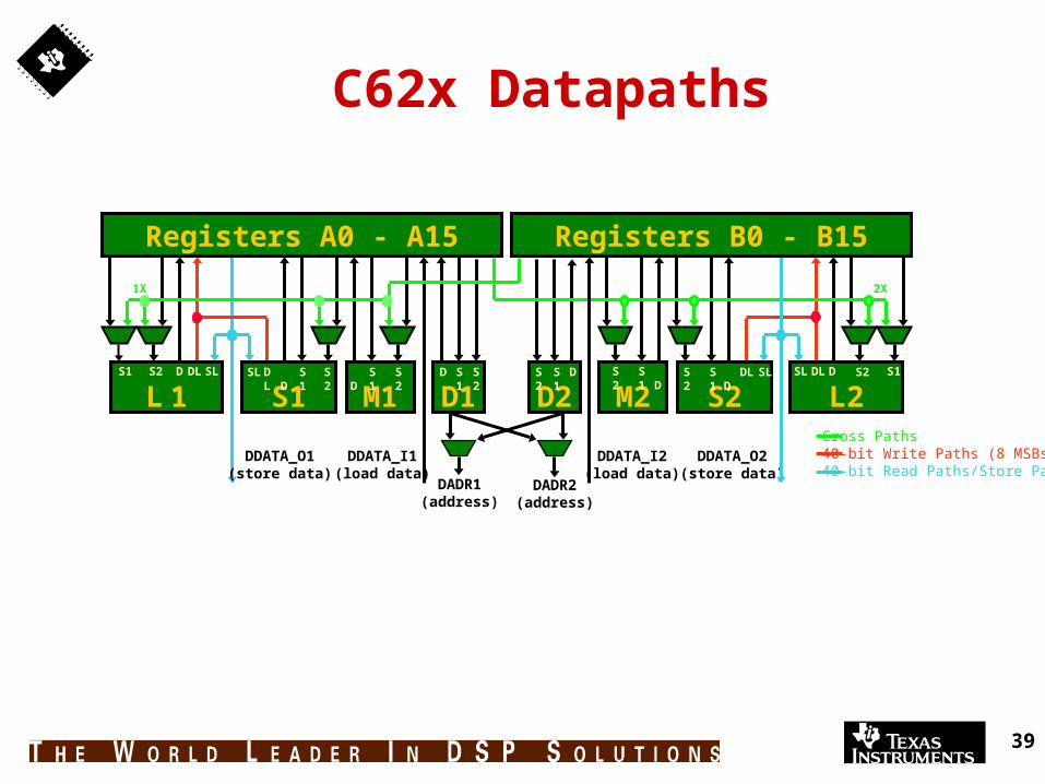
C62x Datapaths
Cross Paths40-bit Write Paths (8 MSBs)40-bit Read Paths/Store Paths
DDATA_I2(load data)
D2DS
1S2
M1 D S
1S2
D1D S
1S2
DDATA_O2(store data)
DADR2(address)
DADR1(address)
DDATA_I1(load data)
DDATA_O1(store data)
2X1X
L 1 S1 S1 S2 DLSL SLD DL S
2S1
D
M2 L2S2 S2 D DL SL SL D DLS
2S1
S1
S2
D S1
Registers B0 - B15Registers A0 - A15
38
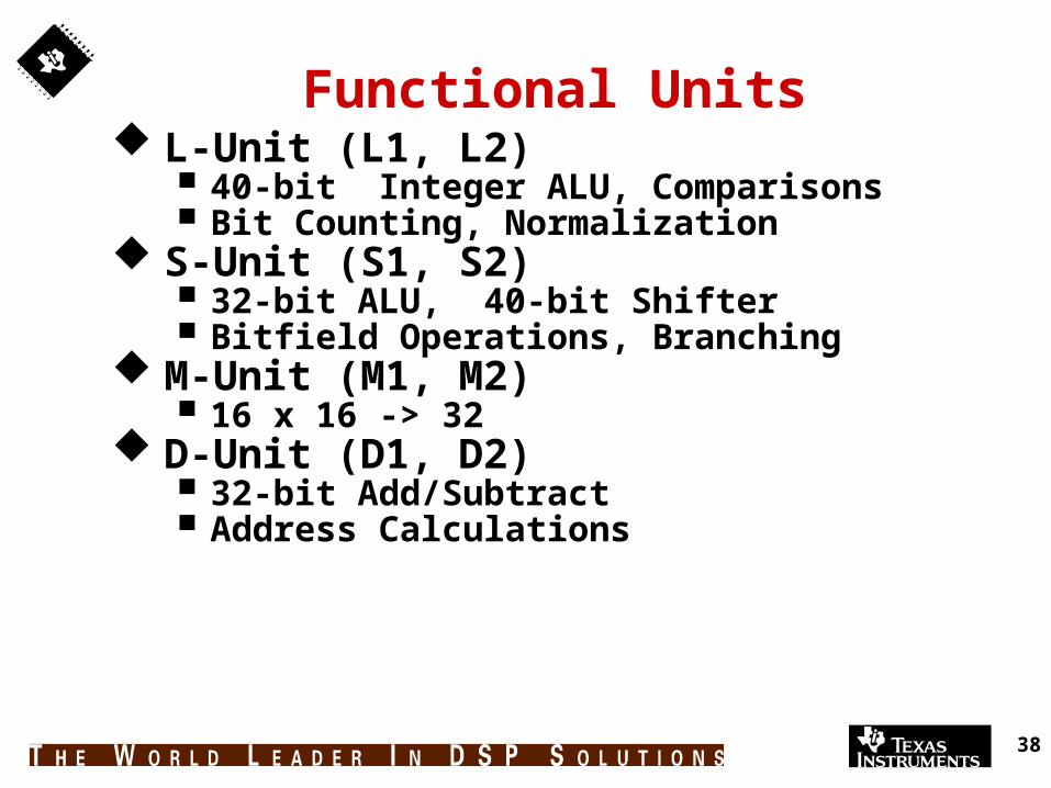
Functional Units L-Unit (L1, L2)
40-bit Integer ALU, Comparisons Bit Counting, Normalization
S-Unit (S1, S2) 32-bit ALU, 40-bit Shifter Bitfield Operations, Branching
M-Unit (M1, M2) 16 x 16 -> 32
D-Unit (D1, D2) 32-bit Add/Subtract Address Calculations
39
C62x Datapaths
Cross Paths40-bit Write Paths (8 MSBs)40-bit Read Paths/Store Paths
DDATA_I2(load data)
D2DS
1S2
M1 D S
1S2
D1D S
1S2
DDATA_O2(store data)
DADR2(address)
DADR1(address)
DDATA_I1(load data)
DDATA_O1(store data)
2X1X
L 1 S1 S1 S2 DLSL SLD DL S
2S1
D
M2 L2S2 S2 D DL SL SL D DLS
2S1
S1
S2
D S1
Registers B0 - B15Registers A0 - A15

40
Example 1
C62x Instruction PackingInstruction Packing Advanced VLIW
Fetch Packet CPU fetches 8 instructions/cycle
Execute Packet CPU executes 1 to 8 instructions/cycle Fetch packets can contain multiple execute packets
Parallelism determined at compile / assembly time
Examples 1) 8 parallel instructions 2) 8 serial instructions 3) Mixed Serial/Parallel Groups
A // B C D E // F // G // H
Reduces Codesize, Number of Program Fetches, Power Consumption
A B C D E F G H
ABCDEFGH
Example 2
A BCDEF G H
Example 3
41
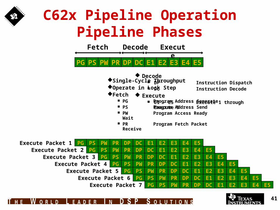
Fetch
PG PS PW PR DP DC E1 E2 E3 E4 E5
Decode Execute
Execute Packet 1
C62x Pipeline OperationPipeline Phases
Single-Cycle ThroughputOperate in Lock StepFetch
PG Program Address Generate PS Program Address Send PW Program Access Ready Wait PR Program Fetch Packet
Receive
Decode DP Instruction Dispatch DC Instruction Decode
Execute E1 - E5 Execute 1 through
Execute 5
PG PS PW PR DP DC E1 E2 E3 E4 E5Execute Packet 2 PG PS PW PR DP DC E1 E2 E3 E4 E5
Execute Packet 3 PG PS PW PR DP DC E1 E2 E3 E4 E5Execute Packet 4 PG PS PW PR DP DC E1 E2 E3 E4 E5
Execute Packet 5 PG PS PW PR DP DC E1 E2 E3 E4 E5Execute Packet 6 PG PS PW PR DP DC E1 E2 E3 E4 E5
Execute Packet 7 PG PS PW PR DP DC E1 E2 E3 E4 E5

42
C62x Pipeline Operation Delay Slots
Delay Slots: number of extra cycles until result is: written to register file available for use by a subsequent instructions Multi-cycle NOP instruction can fill delay slots while
minimizing codesize impact
PGPSPWPRDPDC E1 5 Delay SlotsBranch Target
E1Branches
E1 E2 E3 E4 E5 4 Delay SlotsLoads
E1 E2 1 Delay SlotsInteger Multiply
E1 No DelayMost Instructions
43
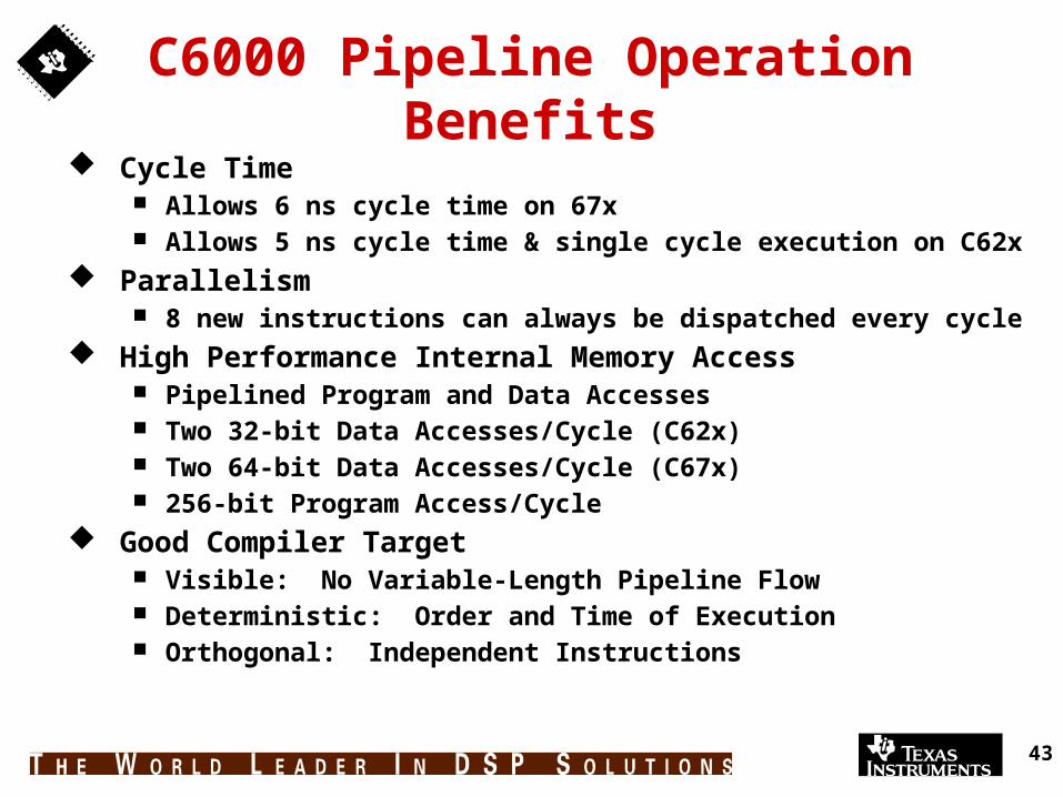
C6000 Pipeline OperationBenefits
Cycle Time Allows 6 ns cycle time on 67x Allows 5 ns cycle time & single cycle execution on C62x
Parallelism 8 new instructions can always be dispatched every cycle
High Performance Internal Memory Access Pipelined Program and Data Accesses Two 32-bit Data Accesses/Cycle (C62x) Two 64-bit Data Accesses/Cycle (C67x) 256-bit Program Access/Cycle
Good Compiler Target Visible: No Variable-Length Pipeline Flow Deterministic: Order and Time of Execution Orthogonal: Independent Instructions

44
C6000 Instruction Set FeaturesConditional Instructions
All Instructions can be Conditional A1, A2, B0, B1, B2 can be used as
Conditions Based on Zero or Non-Zero Value Compare Instructions can allow other
Conditions (<, >, etc) Reduces Branching Increases Parallelism

45
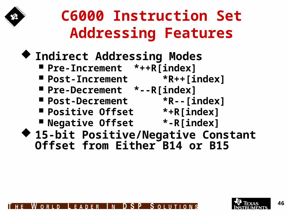
C6000 Instruction Set Addressing Features
Load-Store Architecture Two Addressing Units (D1, D2) Orthogonal
Any Register can be used for Addressing or Indexing
Signed/Unsigned Byte, Half-Word, Word, Double-Word Addressable Indexes are Scaled by Type
Register or 5-Bit Unsigned Constant Index
46
C6000 Instruction Set Addressing Features
Indirect Addressing Modes Pre-Increment *++R[index] Post-Increment *R++[index] Pre-Decrement *--R[index] Post-Decrement *R--[index] Positive Offset *+R[index] Negative Offset *-R[index]
15-bit Positive/Negative Constant Offset from Either B14 or B15

47
C6000 Instruction Set Addressing Features
Circular Addressing Fast and Low Cost: Power of 2 Sizes and
Alignment Up to 8 Different Pointers/Buffers, Up to 2
Different Buffer Sizes Dual Endian Support
48
C67x Architecture
49
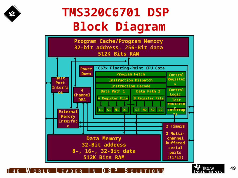
TMS320C6701 DSP Block Diagram
’C67x Floating-Point CPU Core
Data Path 1
D1M1S1L1
A Register File
Data Path 2
L2S2M2D2
B Register File
Instruction Dispatch
Program Fetch
Interrupts
Control Registers
Control Logic
Emulation
Test
External Memory Interface
4 Channel
DMA
Program Cache/Program Memory32-bit address, 256-Bit data
512K Bits RAM
Host Port
Interface
2 Timers
2 Multi-channel buffered
serial ports (T1/E1)
Data Memory32-Bit address
8-, 16-, 32-Bit data512K Bits RAM
Power Down
Instruction Decode

50
TMS320C6701Advanced VLIW CPU (VelociTITM)
1 GFLOPS @ 167 MHz 6-ns cycle time 6 x 32-bit floating-point instructions/cycle
Load store architecture 3.3-V I/Os, 1.8-V internal Single- and double-precision IEEE floating-point Dual data paths
6 floating-point units / 8 x 32-bit instructions
51
TMS320C6701Memory /Peripherals
Same as ’C6201 External interface supports
SDRAM, SRAM, SBSRAM 4-channel bootloading DMA 16-bit host port interface 1Mbit on-chip SRAM 2 multichannel buffered serial ports (T1/E1) Pin compatible with ’C6201

52
ArithmeticLogicUnit
AuxiliaryLogicUnit
MultiplierUnit
’C67x Floating-Point CPU Core
Data Path 1
D1M1S1L1
A Register File
Data Path 2
L2S2M2D2
B Register File
Instruction Decode
Instruction Dispatch
Program Fetch
Interrupts
Control Registers
Control Logic
Emulation
Test
Floating-PointCapabilities
TMS320C67x CPU Core

53
C67x Interrupts 12 Maskable Interrupts Non-Maskable Interrupt (NMI) Interrupt Return Pointers (IRP, NRP) Fast Interrupt Handling
Branches Directly to 8-Instruction Service Fetch Packet 7 Cycle Overhead: Time When No Code is Running 12 Cycle Latency : Interrupt Response Time
Interrupt Acknowledge (IACK) and Number (INUM) Signals
Branch Delay Slots Protected From Interrupts Edge Triggered

54
C67x New InstructionsF
loat
ing
Po
int
Ari
thm
etic
Un
it.L UnitADDSPADDDPSUBSPSUBDPINTSPINTDPSPINTDPINTSPTRUNCDPTRUNCDPSP F
loat
ing
Po
int
Mu
ltip
ly U
nit
.M Unit
MPYSPMPYDPMPYIMPYIDMPY24MPY24H
ABSSPABSDPCMPGTSPCMPEQSPCMPLTSPCMPGTDPCMPEQDPCMPLTDPRCPSPRCPDPRSQRSPRSQRDPSPDP
.S Unit
Flo
atin
g P
oin
t A
uxi
lary
Un
it

55
C67x Datapaths
2 Data Paths 8 Functional Units
Orthogonal/Independent 2 Floating Point Multipliers 2 Floating Point Arithmetic 2 Floating Point Auxiliary
Control Independent Up to 8 32-bit Instructions
Registers 2 Files 32, 32-bit registers total
Cross paths (1X, 2X)
L-Unit (L1, L2) Floating-Point, 40-bit Integer ALU Bit Counting, Normalization
S-Unit (S1, S2) Floating Point Auxiliary Unit 32-bit ALU/40-bit shifter Bitfield Operations, Branching
M-Unit (M1, M2) Multiplier: Integer & Floating-Point
D-Unit (D1, D2) 32-bit add/subtract Addr Calculations
D2DS
1S2
M1 D S
1S2
D1D S
1S2
2X1X
L 1 S1 S1 S2 DLSL SLD DL S
2S1
D
M2 S2 D DL SLS
2S1
S1
S2
D
Registers B0 - B15Registers A0 - A15
L2 S2SL D DL S1

56
C67x Instruction PackingInstruction Packing Enhanced VLIW
Example 1
A B C D E F G H
ABCDEFGH
Example 2
A BCDEF G H
Example 3
Fetch Packet CPU fetches 8 instructions/cycle
Execute Packet CPU executes 1 to 8
instructions/cycle Fetch packets can contain multiple
execute packets Parallelism determined at
compile/assembly time Examples
1) 8 parallel instructions 2) 8 serial instructions 3) Mixed Serial/Parallel Groups
A // B C D E // F // G // H
Reduces Codesize Number of Program Fetches Power Consumption

57
C67x Pipeline OperationPipeline Phases
Fetch
PG PS PW PR DP DC E1 E2 E3 E4 E5
Decode Execute
E6 E7 E8 E9 E10
PG PS PW PR DP DC E1 E2 E3 E4 E5 E6 E7 E8 E9 E10
PG PS PW PR DP DC E1 E2 E3 E4 E5 E6 E7 E8 E9 E10
PG PS PW PR DP DC E1 E2 E3 E4 E5 E6 E7 E8 E9 E10
PG PS PW PR DP DC E1 E2 E3 E4 E5 E6 E7 E8 E9 E10
PG PS PW PR DP DC E1 E2 E3 E4 E5 E6 E7 E8 E9 E10
PG PS PW PR DP DC E1 E2 E3 E4 E5 E6 E7 E8 E9 E10
PG PS PW PR DP DC E1 E2 E3 E4 E5 E6 E7 E8 E9 E10
Execute Packet 1
Execute Packet 2
Execute Packet 3
Execute Packet 4Execute Packet 5
Execute Packet 6
Execute Packet 7
Operate in Lock StepFetch
PG Program Address Generate
PS Program Address Send PW Program Access Ready
Wait PR Program Fetch Packet
Receive
Decode DP Instruction Dispatch DC Instruction Decode
Execute E1 - E5 Execute 1 through
Execute 5 E6 - E10 Double Precision
Only

58
C67x Pipeline OperationDelay Slots
PG PS PW PR DP DC E1 5 Delay SlotsBranch Target
E1Branches
E1 E2 E3 E4 4 Delay SlotsLoads
E1 E2 3 Delay SlotsSingle-Precision
E1 No DelayMost Integer
E5
E3 E4
Delay Slots: number of extra cycles until result is: written to register file available for use by a subsequent instructions Multi-cycle NOP instruction can fill delay slots while
minimizing codesize impact
59
ControlRegistersEmulation
Registerfile
Program Fetch & Dispatch
L-Unit 1Arithmetic Logic Unit
S-Unit 1Auxiliary Logic Unit
D-Unit 1Data Load/
Store
DecodeRegister
file
M-Unit 2Multiplier
Unit
L-Unit 2Arithmetic Logic Unit
S-Unit 2Auxiliary Logic Unit
D-Unit 2Data Load/
Store
’C62x CPU
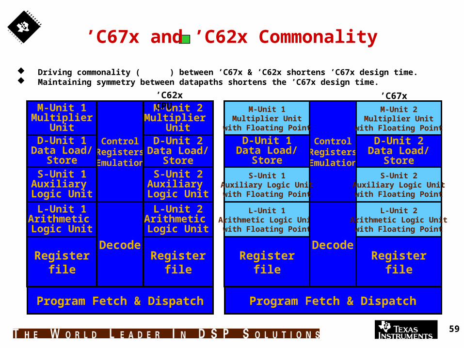
’C67x CPUM-Unit 1
MultiplierUnit
’C67x and ’C62x Commonality
Driving commonality ( ) between ’C67x & ’C62x shortens ’C67x design time. Maintaining symmetry between datapaths shortens the ’C67x design time.
ControlRegistersEmulation
Registerfile
Program Fetch & Dispatch
L-Unit 1Arithmetic Logic Unit
with Floating Point
S-Unit 1Auxiliary Logic Unitwith Floating Point
D-Unit 1Data Load/
Store
DecodeRegister
file
M-Unit 2Multiplier Unit
with Floating Point
L-Unit 2Arithmetic Logic Unit
with Floating Point
S-Unit 2Auxiliary Logic Unitwith Floating Point
D-Unit 2Data Load/
Store
M-Unit 1Multiplier Unit
with Floating Point

60
TMS320C80 MIMD MULTIPROCESSORTexas Instruments - 1996

61
Copyright 1999Copyright 1999