Embed Size (px)
Citation preview

1
InGaAs/InP DHBTs in a planarized, etch-back technology for base contacts
Vibhor Jain, Evan Lobisser, Ashish Baraskar, Brian J Thibeault, Mark RodwellECE Department, University of California, Santa Barbara, CA 93106-9560
D Loubychev, A Snyder, Y Wu, J M Fastenau, W K LiuIQE Inc., 119 Technology Drive, Bethlehem, PA 18015
[email protected], 805-893-3273
International Symposium on Compound Semiconductors 2011

2
Outline
• HBT Scaling Laws
• Refractory base ohmics
• Fabrication
• DHBT – Epitaxial Design and Results
• Summary

3
Ohmic contacts
Lateral scaling
Epitaxial scaling
Bipolar transistor scaling laws
To double cutoff frequencies of a mesa HBT, must:
(emitter length Le)
We
Tb TcWbc
Keep constant all resistances and currentsReduce all capacitances and transit delays by 2
RCf tr
2
1
exitbnbb vTDT 22satcc vT 2
eex AR /contact
contacts
contactsheet 612 AL
W
L
WR
e
bc
e
ebb
cccb /TAC 2
cbmax, /)( cbieeffc TVAvI
effcbeffbb CR
ff
,,max 8

4
InP bipolar transistor scaling roadmap
Emitter
256 128 64 32 Width (nm)
8 4 2 1 Access ρ (Ω·µm2)
Base
175 120 60 30 Contact width (nm)
10 5 2.5 1.25 Contact ρ (Ω·µm2)
Collector 106 75 53 37.5 Thickness (nm)
Current density 9 18 36 72 mA/µm2
Breakdown voltage 4 3.3 2.75 2-2.5 V
fτ520 730 1000 1400 GHz
fmax850 1300 2000 2800 GHzPe
rfor
man
ceD
esig
n
Rodwell, Le, Brar, Proceedings of IEEE, 2008

5
• Pd contacts diffuse in base (p-InGaAs)• Contact resistance ↑ for thin base• Limits base thickness
Scaling Limitation
100 nm InGaAs grown in MBE
15 nm Pd diffusion
Need for non-diffusive, refractory base metal
Contact diffusionTEM by E Lobisser
Ashish Baraskar
6
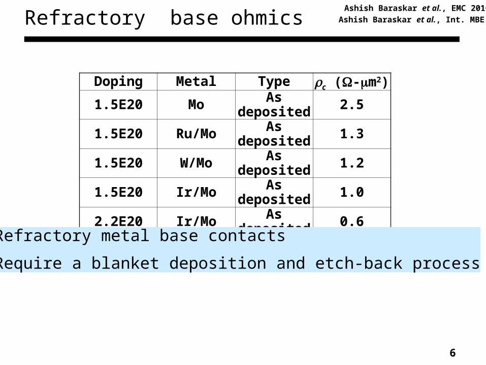
Refractory base ohmics
Doping Metal Type c (-m2)1.5E20 Mo As deposited 2.51.5E20 Ru/Mo As deposited 1.31.5E20 W/Mo As deposited 1.21.5E20 Ir/Mo As deposited 1.02.2E20 Ir/Mo As deposited 0.62.2E20 Ir/Mo Annealed 0.8
Ashish Baraskar et al., EMC 2010
Refractory metal base contacts
Require a blanket deposition and etch-back process
Ashish Baraskar et al., Int. MBE 2010

7
Emitter process flow
Mo contact to n-InGaAs for emitter
W/TiW/SiO2/Cr dep
SF6/Ar etch
SiNx Sidewall
SiO2/Cr removal
InGaAs Wet Etch
Second SiNx Sidewall
InP Wet Etch
W/TiW interface acts as shadow mask for base lift off
Collector formed via lift off and wet etch
BCB used to passivate and planarize devices
Mo
base
N- collector
InP substrate
sub collector
emitteremitter cap
n+ InGaAs
n InP
emitter capemitter
base
SiO2/Cr
TiW
MoW
SiN (SW)
emitterbase base

8
W
MoInGaAs
p+ InGaAs Base
Ti0.1W0.9
InP
W
MoInGaAs
p+ InGaAs Base
Ti0.1W0.9
InP
Base process flow – I
PR
Blanket refractory metal PR Planarization
Isotropic Dry etch of metal
Removes any Emitter-Base short

9
W
MoInGaAs
p+ InGaAs Base
Ti0.1W0.9
InP
W
MoInGaAs
p+ InGaAs Base
Ti0.1W0.9
InP
SiNx
Base process flow – II
Lift-off Ti/Au
Low base metal resistance
Blanket SiNx mask
Etch base contact metal in the field

10
Base Planarization
Planarization: Emitter projectingfrom PR for W dry etch
Etch Back
Planarization Boundary

11
Epitaxial Design
T(nm) Material Doping (cm-3) Description
10 In0.53Ga0.47As 81019 : Si Emitter Cap
15 InP 51019 : Si Emitter
15 InP 21018 : Si Emitter
30 InGaAs 9-51019 : C Base
4.5 In0.53Ga0.47 As 91016 : Si Setback
10.8 InGaAs / InAlAs 91016 : Si B-C Grade
3 InP 6 1018 : Si Pulse doping
81.7 InP 91016 : Si Collector
7.5 InP 11019 : Si Sub Collector
7.5 In0.53Ga0.47 As 21019 : Si Sub Collector
300 InP 21019 : Si Sub Collector
Substrate SI : InP
Vbe = 1 V, Vcb = 0.7 V, Je = 25 mA/m2
-2.5
-2
-1.5
-1
-0.5
0
0.5
1
1.5
0 50 100 150 200
En
erg
y (e
V)
Distance (nm)
Emitter
Collector
Base
Low Base doping
Good refractory ohmics not possible
Pd/W contacts used

12
Results - DC Measurements
BVceo = 2.4 V @ Je = 1 kA/cm2
β = 26
JKIRK = 21 mA/m2
@Peak f,fmax
Je = 17.9 mA/m2
P = 30 mW/m2
Gummel plot
Common emitter I-V
0
10
20
30
0 0.5 1 1.5 2 2.5
J e (
mA
/m
2)
Vce
(V)
P = 25 mW/m2
Peak f/f
max
Ib = 200 A
Ib,step
= 200 A
10-7
10-5
10-3
10-1
0 0.2 0.4 0.6 0.8 1
I c,
I b (
A)
Vbe
(V)
Ic
Ib
Solid Line: Vcb
= 0 V
Dashed Line: Vcb
= 0.7 V
nc = 1.76
nb = 3.29

13
1-67 GHz RF Data
Ic = 22.4 mA
Vce = 1.67 V
Je = 17.9 mA/m2
Vcb = 0.7 V
Single-pole fit to obtain cut-off frequencies
0
10
20
30
109 1010 1011 1012
Gai
n (
dB
)
freq (Hz)
U
H21
MSG
fmax
= 690 GHz
f = 410 GHz
Aje
= 0.22 × 5.7 m2

14
Equivalent Circuit
Hybrid- equivalent circuit from measured RF data
Rex = 6 m2
Ccb,x = 4.48 fF
Ccb,i = 1.3 fF
Rcb = 17 k
Rc = 1.7
Rex = 4.7
Rbe = 42
Rbb = 24
Cje + Cdiff = (15 + 241) fF gmVbee-j
0.73Vbeexp(-j0.15ps)
Base
Emitter
Col
Ccg = 6.8 fF
Ccb,x = 4.48 fF
Ccb,i = 1.3 fF
Rcb = 17 k
Rc = 1.7
Rex = 4.7
Rbe = 42
Rbb = 24
Cje + Cdiff = (15 + 241) fF gmVbee-j
0.73Vbeexp(-j0.15ps)
Base
Emitter
Col
Ccg = 6.8 fF
freq (1.000GHz to 67.00GHz)
S(1
,1)
freq (100.0MHz to 67.00GHz)
S_p
aram
eter
_Dee
mbe
d_P
NA
..S11
dS
_par
amet
er_D
eem
bed_
PN
A..S
22d
S(1
,2)*
5S
(2,1
)/12
S_p
aram
eter
_Dee
mbe
d_P
NA
..S12
d*5
S_p
aram
eter
_Dee
mbe
d_P
NA
..S21
d/12
S(2
,2)
S21/12
S12x5
S11S22
--- : Measured x : Simulated
freq (1.000GHz to 67.00GHz)
S(1
,1)
freq (100.0MHz to 67.00GHz)
S_p
aram
eter
_Dee
mbe
d_P
NA
..S11
dS
_par
amet
er_D
eem
bed_
PN
A..S
22d
S(1
,2)*
5S
(2,1
)/12
S_p
aram
eter
_Dee
mbe
d_P
NA
..S12
d*5
S_p
aram
eter
_Dee
mbe
d_P
NA
..S21
d/12
S(2
,2)
S21/12
S12x5
S11S22
--- : Measured x : Simulated

15
TEM
Large undercut in base mesa
Pd/W adhesion issue
High Rbb
Low fmax 0.1 m
Pd/W adhesion issue
Large mesa undercut

16
Summary
• Demonstrated a planarized, etch back process for refractory base contacts
• Demonstrated DHBTs with peak f / fmax = 410/690 GHz
• Higher base doping, thinner base and refractory base ohmics needed to enable higher bandwidth devices
17
Questions?
Thank You
This work was supported by the DARPA THETA program under HR0011-09-C-006.
A portion of this work was done in the UCSB nanofabrication facility, part of NSF funded NNIN network and MRL Central Facilities supported by the MRSEC Program of the NSF under award No. MR05-20415