Embed Size (px)
Citation preview

Design and Test of a Planarized High PowerDensity 100 kW SiC Traction Inverter with 1kV
DC-Link
Li Yang, Yukun Luo, Radha Sree Krishna Moorthy, Dhrubo Rahman, Wensong Yu, Iqbal HusainFREEDM System Center
North Carolina State University
Email: {lyang20,yluo9,rkrish12,drahman,wyu2,ihusain2}@ncsu.edu
Abstract—A SiC MOSFET based 1kV DC-link planarizedtraction inverter is designed to achieve high power density andhigh common mode noise immunity of the gate driver. To achievehigh power density, a planarized structure is adopted to reducethe overall height of the whole system. Significantly, PCB basedbusbar, gate driver planar transformer and shunt-based currentsensor are the main concepts for planarized inverter design.Moreover, a split gate driver concept is used to shrink the overallsize of inverter and reduce driving loop inductance as well. Anoptimized planar transformer winding layout has been used toreduce the coupling capacitance between primary and secondaryside in order to achieve high common mode noise immunity. Theinverter is designed for 100kW continuous power and has beentested with a novel closed-loop high power circulating strategythat requires only a small rating DC power supply. Testingresults verify the design concepts and the high performance ofthe traction inverter.
Index Terms—SiC MOSFET, traction inverter, low profile, highcommon mode transient immunity(CMTI), high power density.
I. INTRODUCTION
Silicon Carbide(SiC) MOSFET as a wide bandgap device
provides a lot of merits that are especially favored by electrical
vehicle (EV) industry. Compared with Si IGBT, SiC device has
lower switching and conduction losses that is important for EV
mileage extension. The high junction temperature operation
capability makes it possible to design integrated powertrain
with reduced cooling requirement. High switching frequency
of the SiC device reduces size of passive components in the
powertrain system including DC-link capacitor, boost inductor
and EMI filter. Because of the features of SiC device, overall
size of the powertrain can be reduced, which makes SiC
device a good candidate to achieve high power density for
EV powertrain.
High power density design, among high temperature op-
eration and high efficiency operation, has been one of the
main focus of researches on SiC traction inverter. A 35kW
SiC traction inverter is designed in [1] with power density of
70kW/L. The SiC module is designed with Schottky Barrier
Diode(SBD) removed, which reduces switching loss and the
size of heat sink. In [2] and [3], 50kW traction inverters
are designed with SiC JFET and SiC MOSFET, respectively.
Both of the designs have gate assistant circuit to achieve
fast switching of SiC device. The power density achieved
by the works are 8.5kW/kg and 26kW/kg, respectively. The
work in [4] reports a liquid-cooled 55kW traction inverter
designed with front-end boost stage, the inverter is designed
with four six-pack SiC MOSFETs and features a planarized
structure, overall power density achieved is 12.1kW/L. In [5],
Fraunhofer developed liquid cooled 60kW SiC inverter for
high speed drives. The design uses a high DC-link voltage
(900Vdc) and power module with integrated gate driver that
can switch at 100kHz with low loss. The achieved power
density is 160kW/L. Mitsubishi developed HEV powertrain
with both motor/generator inverter and front-end boost stage
at a total power level of 430kVA[6]. The power module
is designed to have low commutation loop inductance that
enables fast switching, direct soldering of the module on
heat sink improves the thermal conductivity. Achieved power
density of the design is 86kVA/L. In [7], Wolfspeed developed
250kW traction inverter using off-the-shelf low profile low
inductance full SiC module. The inverter is reported to operate
under 150°C ambient temperature and achieves power density
of 15.6kW/kg.
Recently, high DC-link voltage traction inverter has been
introduced to EV powertrain design. While the majority
passenger electrical vehicle manufactures now adopts 400V
system for the traction inverter, which has a DC-link voltage
of 150V-450V, an 800V system which has DC-link of up
to 870V has come into market and provides benefits to the
EV powertrain[8][9]. Compared with 800V system, the 400V
system needs to operate with much higher phase current that
increases temperature and loss of the busbar and power cable.
Moreover, high current operation also reduces reliability of the
DC-link capacitors. As analyzed in [10], the DC-link ripple
current directly relates with the magnitude of AC current out-
put. Therefore, DC-link capacitor of the high current inverter
needs to sink and source high ripple current, which is usually
achieved by paralleling more capacitor cells at the sacrifice of
power density and cost.
In this paper, the design optimizations on the busbar, gate
driver and current sensor are discussed. The paper presents
a planarization design method that can achieve high power
density of the inverter as shown in Fig. 1. The inverter is
designed for 100kW continuous power with 1kV DC-link
to investigate both the benefits and issues of high DC-link
978-1-4799-7312-5/18/$31.00 ©2018 IEEE 3864

traction inverter as discussed in [8]. At last, a high power
circulating test strategy is used to test the inverter up to 100kW
without the need of high rating DC power supplies and load
banks.
Fig. 1: Assembly view of the planar structure.
II. PCB BUSBAR DESIGN FOR 1.7 KV SIC MODULE
The 1kV DC-link design is achieved using Wolfspeed’s
state-of-the-art 1.7kV/8mΩ full SiC MOSFET module HT-
3231. The module shares the same high performance 62mm
half-bridge package as Wolfspeed’s off-the-shelf 1.2kV/3.7mΩmodule CAS325M12HM2. A detailed ANSYS Q3D modeling
and parasitic inductance simulation has been conducted for
the used module in [11], module inductance from DC+ to
DC- is 10.48nH at 10MHz. The modeling of the 1.2kV/3.7mΩmodule is shown in Fig.2.
Fig. 2: Modeling of off-the-shelf 1.2kV/3.7mΩ module in
ANSYS Q3D.
A. Characteristic Impedance MinimizationAs the interconnection of power components of the inverter,
a low characteristic impedance of busbar is critical to attenuate
high frequency noise and EMI. Characteristic impedance is
expressed by (1):
Z =
√L
C=
√Lp + Ln − 2Lm
Cdd(1)
where Lp and Ln are the self-inductance of DC+ and DC-
planes of the busbar, Lm is the mutual-inductance and Cdd is
the coupling capacitance of the planes. Modeling DC planes
of the busbar as two parallel copper sheets with the geometries
shown in Fig.3, the parasitic parameters of the busbar can be
calculated by (2).
Fig. 3: Modeling busbar by parallel copper sheets.
Lp,n =μ0μrl
π(1
8+
2d
d+ w) (h � w, d � w)
Lm =μ0μrl · d
π√4(d+ h)2 + kW 2
cos θ
Cdd = ε0εrw · lh
(2)
where μ0, μr are the vacuum permeability and the relative
permeability of the insulating material, ε0, εr are electric
constant and relative static permittivity of the insulating ma-
terial and θ the angle between the planes[12]. According to
(2), Lp,n can be minimized by decreasing l and d while
increasing w. Lm can be maximized by increasing l and dwhile decreasing h. Cdd can be maximized by increasing land w while decreasing h. There are trade-offs to be made
on l and d, but the width w and distance h of the DC copper
planes needs to be maximized and minimized, respectively,
to reduce the characteristic impedance. The designed PCB
busbar uses 4oz. copper each layer to provide enough current
conduction capability and increase Lm, the busbar is designed
for 8 layers with the stack shown in Fig.4. By placing DC
planes adjacently, h is reduced and Lm, Cdd are increased.
By designing two sets of DC planes, the current conduction
capability of the busbar is increased as well as the Cdd.
Fig. 4: Layer stack of the designed PCB busbar.
A chasis ground layer is also added for the PCB busbar
that has two benefits: (1)the chasis ground helps to reduce
the commutation loop inductance. The result has been verified
by ANSYS Q3D simulation for the busbar with and without
the chasis ground; (2)the chasis ground forms Y capacitor
with both the AC and DC planes, which helps attenuate high
3865

frequency EMI noise from the inverter[13]. As the overlap
between DC planes are maximized to increase the stray
capacitance, the overlap between the AC planes and DC planes
are minimized. The reason is that these planes are essentially
the drain and source for the top and bottom switches, so
overlapping them will increase the output capacitance Coss.
Therefore, switching speed decreased and switching loss in-
creased if the overlap is enlarged. The overlap area for the
designed busbar is minimized for current conduction capability
of 100A.
B. Commutation Loop Optimization
Commutation loop inductance minimization is critical for
the busbar design. Usually, the commutation loop is formed by
the DC-link capacitors, the conduction path inside the power
module and the stray inductance on the busbar between them.
Low ESL DC-link capacitor, optimized busbar layout and high
performance module all help to reduce the loop inductance.
Adding low ESL decoupling capacitor in close vicinity to
the module is another effective method to reduce the loop
inductance. The design is shown in Fig.5 where Loop 1 is
formed by DC-link capacitors and Loop 2 is formed by the
decoupling capacitors.
Fig. 5: Layout of commutation loops for two phases on the
PCB busbar.
Busbar design adopting a central electrolytic DC-link ca-
pacitor can result in unsymmetrical commutation loops for
different phases and cause the highest Vds overshoot as well
as switching loss for one particular phase. Therefore, the
commutation loops for three phase voltage source inverter
should be designed as symmetrical as possible especially
for high power applications. Also shown in Fig.5, two film
DC-link capacitors totally 54uF and six ceramic decoupling
capacitors are designed identically for each phase. The total
inductance of commutation loop Loop 2 is 12.8nH at 10MHz.
C. Overall Design of the Busbar
The PCB based busbar for 100kW SiC traction inverter is
designed based on the optimizations and methods discussed
above, the top and side view of the busbar are shown in
Fig.6(a) and Fig.6(b). The layout of three phase circuits are
identical and totally 162uF DC-link capacitor is designed for
the busbar.
(a)
(b)
Fig. 6: 3D layout of the PCB busbar (a) top view (b) side
view.
III. LOW PROFILE GATE DRIVER
A. Gate Driver Power Supply Architecture
The key concept on optimizing gate driver isolation trans-
former is by high frequency operation. Increasing transformer
operating frequency, smaller core can be used which makes
low profile planar transformer possible. High frequency opera-
tion also reduces the number of turns needed for the windings,
which reduces the coupling capacitance between the windings
as a result.
To achieve high frequency operation, a transformer driver
MAX13256 from Maxim is selected. Architecture of the
designed gate driver power supply is shown in Fig.7 following
[14]. The transformer driver converts 24V DC to ±24V square
wave at a frequency around 450kHz. The high frequency AC
link is then shared by two planar transformers for the top and
bottom driver circuits and rectified to generate +19V/-5V rails.
High frequency core material 3F35 is chosen for low core
loss. In [15], a modified core loss density model is proposed
for square wave excited transformer and the predicted core
loss under square wave excitation is given by:
Pcore =8
π2[4D(1−D)]γ+1KfαBβ (3)
where D=0.5 is fixed by MAX13256, γ =−0.12 is the curve
fitting coefficient for 3F35 material under 500kHz squre wave
excitation and KfαBβ is the core loss predicted by Steinmetz
equation under sinusoidal excitation, which is given in core
3866

Fig. 7: Architecture of the designed gate driver power supply.
material datasheet. An EI core combination E18/4/10/R-3F35
and PLT18/10/2/S-3F35 from Ferroxcube are chosen for the
planar transformer, assuming 0.1W loss on the core, according
to8
π2[4D(1−D)]γ+1KfαBβ =
0.1× 10⁻³
Ve
KfαBβ = 148.6kW/m3, where Ve = 830mm3 is the effec-
tive core volume of the selected EI core. The corresponding
peak flux density can be found to be ΔB = 60mT from
the power loss vs. peak flux density curve of the material.
Using (4), the number of turns for the transformer can be
calculated, where v ·Δt = 26.4V · μs is the applied volt-sec
and Ae = 40mm2 is the effective core area.
N =v ·Δt
2 ·Ae ·ΔB= 5.5 (4)
B. Transformer Inter-winding Capacitance Minimization
Isolation transformer with low inter-winding capacitance
is critical for SiC device based inverter that operates with
high dv/dt. The inter-winding capacitance of transformer
consists of two contributors [16]. As shown in Fig.8, the Cww
is the winding-winding capacitance formed by primary and
secondary windings; the Cwcw is the winding-core-winding
capacitance formed by the windings and the core. To reduce
the inter-winding capacitance, both Cww and Cwcw needs to
be minimized.
Fig. 8: Two stray capacitance components contributing the
total coupling capacitance.
The winding layout is on a six layer PCB. To decide the
inter-winding capacitance contributed by Cww, three layouts
for N=6, 5, and 4 are first simulated in ANSYS Q3D. As
shown in Fig.9, the inner windings are for primary side and
the outer windings are for secondary side. For N=6, two
turns are designed on each layer, while for N=5 and 4,
one turn is on each layer. The simulated inter- and intra-
Fig. 9: Layout of the PCB transformer for N=6, 5, 4 from left
to right.
winding capacitances are tabulated in Table I. Compare the
results for N=6 and N=5,4, a significant reduction on inter-
winding capacitance (Cww) is achieved because of the increase
on distance between primary and secondary windings. The
winding-core-winding capacitance (Cwcw) is also expect to
reduce, because with less turns on each layer, the overlap area
between the windings and core is reduced. Compare the results
for N=5 and N=4, there are minor reduction on Cww because
the pattern for the two layouts are similar, both the Cww and
Cwcw will be similar.
TABLE I: Stray capacitance comparison for N=6, 5 and 4.
Intra-winding Inter-winding
No. of turns Capacitance(pF) Capacitance w/o core
Primary/Secondary (pF)
4 3.3/4.3 2.3
5 3.5/4.6 2.5
6 5.1/6.2 4.1
Transformer with both N=6 and N=5 are fabricated for
experimental tests. Testing results are tabulated in Table II. The
results verified the reduction on inter-winding capacitance for
the transformer both with and without the planar core. There
is a drop on overall efficiency for N=5 design because with
one turn less, peak flux density for the core gets increased,
which increases the core loss. Moreover, with just one turn per
layer, more vias are used for the layout and the winding loss
also increases. To have the minimal inter-winding capacitance
design for the transformer while not increasing the core loss
significantly, N=5 layout is chosen for the transformer. Final
design achieves <5pF coupling capacitance and 4mm on-
board height.
The fabricated gate driver board for a single module is
shown in Fig.10.
C. Driver Loop Inductance Minimization
Driving loop inductance minimization is another critical
aspect for gate driver optimization. High loop inductance can
cause severe LCR oscillation in the driving loop that may
lead to gate break down, it can also deteriorate shoot-through
fault caused by cross-talk of top and bottom switch in a phase
leg[17]. To minimize driver loop inductance, self-inductance of
forward-path and return-path of both charging and discharging
3867
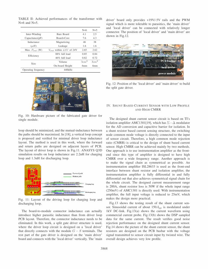
TABLE II: Achieved performances of the transformer with
N=6 and N=5.
N=6 N=5
Inter-Winding Bare Board 4.1 2.5
Capacitance(pF) Board+Core 7.6 4.3
Inductance Magnetizing 46 38
(μH) Leakage 1.6 1.6
Max. Pout (W) Vout within ±1V of 24V 2.65 2.62
Efficiency88% full load 0.85 0.84
46% full load 0.82 0.72
SizeVolume 3cm3 3cm3
On-board Height 4mm 4mm
Operating frequency 440kHz
Fig. 10: Hardware picture of the fabricated gate driver for
single module.
loop should be minimized, and the mutual-inductance between
the paths should be maximized. In [18], a vertical loop concept
is proposed and verified for minimal driver loop inductance
layout. The method is used in this work, where the forward
and return paths are designed on adjacent layers of PCB.
The layout of driver loop is shown in Fig.11. ANASYS Q3D
simulation results on loop inductance are 2.2nH for charging
loop and 1.3nH for discharging loop.
Fig. 11: Layout of the driving loop for charging loop and
discharging loop.
The board-to-module connector inductance can actually
introduce higher parasitic inductance than from driver loop
PCB layout. Therefore, the connector inductance needs to be
eliminated. In this work, a split gate driver structure is used,
where the driver loop circuit is designed on a ’local driver’
that directly connects with the module G − S terminals. The
rest part of the gate driver is designed on the ’main driver’
board and connects with the ’local driver’ vertically. The ’main
driver’ board only provides +19V/-5V rails and the PWM
signal which is more tolerable to parasitics, the ’main driver’
and ’local driver’ can be connected with relatively longer
connector. The position of ’local driver’ and ’main driver’ are
shown in Fig.12.
Fig. 12: Position of the ’local driver’ and ’main driver’ to build
the split gate driver.
IV. SHUNT BASED CURRENT SENSOR WITH LOW PROFILE
AND HIGH CMRR
The designed shunt current sensor circuit is based on TI’s
isolation amplifier AMC1301[19], which has Σ−Δ modulator
for the AD conversion and capacitive barrier for isolation. In
a shunt resistor based current sensing structure, the switching
node common mode voltage is directly connected to the input
of sensor circuit. Therefore, a high common mode rejection
ratio (CMRR) is critical to the design of shunt based current
sensor. High CMRR can be achieved mainly by two methods.
One approach is to use instrumentation amplifier as the front-
end since this type of amplifier is designed to have high
CMRR over a wide frequency range. Another approach is
to make the signal chain as symmetrical as possible. An
instrumentation amplifier ISL28633 is used as the front-end
interface between shunt resistor and isolation amplifier, the
instrumentation amplifier is fully differential in and fully
differential out that also achieves symmetrical signal chain for
the whole circuit. The designed current measurement range
is 200A, shunt resistor loss is 50W if the whole input range
(250mV) of AMC1301 is directly used. With instrumentation
amplifier, the full input voltage is reduced to 25mV, which
makes the design more practical.
Fig.13 shows the testing result of the shunt current sen-
sor. Sinusoidal current of about 150App is modulated under
1kV DC-link. Fig.13(a) shows the current waveform using
commercial current probe. Fig.13(b) shows the DSP sampled
data for the same current. The result verifies good noise
rejection performance on the designed shunt current sensor.
Fig.14 shows the picture of the shunt current sensor, the shunt
resistors are designed on the PCB busbar with the voltage
signal transmitted to sensor circuit input by twisted wire. The
overall design achieves very low profile.
3868

(a)
(b)
Fig. 13: Testing result of the shunt current sensor (a)output
current measured with commercial probe (b)DSP sampled data
plotted in MATLAB.
Fig. 14: Hardware picture of the low profile shunt based
current sensor.
V. BACK-TO-BACK INVERTER HIGH POWER CIRCULATING
TEST METHOD
In this section a new testing strategy on high power traction
inverter is discussed. Conventional method of using LR load
for inverter testing requires three phase load bank and high
power DC supply. To change power factor of inverter output,
different fundamental frequency, inductor and resistor values
have to be calculated accordingly. The method proposed in this
work achieves power circulating between the source inverter
and the DUT, therefore large load bank is not needed and only
a low power DC supply is used to hold the DC bus. By doing
closed-loop current control, power factor can be conveniently
changed.
The setup consists of two inverters connected back-to-back
with three inductors in between as shown in Fig.15. The setup
can be regarded as a traction inverter driving a three-phase AC
motor with back EMF. Therefore, the concept of field oriented
control on three phase AC motor can be applied on the power
circulating strategy. First, the three phase sinusoidal back EMF
voltages Ea, Eb and Ec are synthesized by a rotating space
vector E in α−β coordinate. The space vector has magnitude
E and rotates at fundamental frequency ω. The driving voltage
Va, Vb and Vc can also be denoted by space vector V in α−βcoordinate. Their differential voltage is applied on the inductor.
By placing the two space vectors in the synchronous reference
frame of the driving inverter and aligning the back EMF vector
E on the d-axis of the synchronous reference frame, the input
and output apparent power as well as power factor of the two
inverters can be controlled by the phase and magnitude of
current vector I . Specifically, if Iq = 0, unity power factor
operation on the DUT can be achieved. This concept is shown
in Fig.16.
Fig. 15: Hardware setup of the high power circulating test
strategy.
Fig. 16: Demonstration of the circulating strategy in syn-
chronous reference frame.
Using inverse Clarke Transformation, the three phase EMF
in stationary coordinate can be obtained as shown in (5) ,
where θ = wt. The back EMF are modulated by SPWM in
open loop.
⎡⎣Ea
Eb
Ec
⎤⎦ =
⎡⎢⎣
1 0
− 12
√32
− 12 −
√32
⎤⎥⎦[E · cos θE · sin θ
](5)
The d−q model of the virtual motor in synchronous reference
frame can be expressed by (6) where Vd and Vq are the
terminal voltages, Ed and Eq are the back EMF voltages in
d− q frame. The current controller can be designed based on
the model as shown in Fig.17. The Vd and Vq are generated
3869

by PI regulators with compensation terms. A zero-sequence
current suppressor is also added to the controller to mitigate
the zero-sequence current issue inherent to the back-to-back
inverter setup[20]-[22].
Vd = Ldiddt
+ ωLiq + Ed
Vq = Ldiqdt
− ωLid + Eq
(6)
Fig. 17: Block diagram of the current controller.
For practical implementation, two types of synchronization
need to be implemented. As the d axis of the synchronous
reference frame need to be aligned with the back EMF vector
E , the rotation angle θ used for both controllers must be
well synchronized. Failing to do so will cause steady state
error on the output. Moreover, the PWM carriers of both
controllers need to be synchronized to reduce the ripple
current on the load inductors and system loss[23]. An external
synchronization controller generates square wave signal at
fundamental frequency to synchronize both the transformation
angle and PWM carrier. Hardware implementation for the
synchronization and experimental results on zero sequence
current reduction are elaborated in[24].
The 100kW full continuous power operation of the SiC
inverter is tested by the back-to-back circulating method
as shown in Fig.18. The inverter is operated under 1kV
DC-link, 160Apk phase current and 30kHz switching fre-
quency. Fig.18(a) shows the three phase sinusoidal waveform,
Fig.18(b) shows the DC-link current waveform with mean
value of 100A, and the Vds waveform with an overshoot of
18% maximum. With the back-to-back circulating test strategy,
the 1kV DC power supply only needs to provide around 5kW
output to the whole system, which is the total loss generated
by the system. The results also verifies the performance of the
designed shunt based current sensor working under 100kW
condition.
VI. CONCLUSION
This paper discusses the design on a 100kW SiC traction
inverter with 1kV DC-link. To achieve low profile, planar
structure is adopted. The optimizations on the PCB busbar
helps to achieve low characteristic impedance, symmetrical
commutation loop and low loop inductance that is critical to
reduce the Vds overshoot. The planar transformer significantly
reduces overall height of the gate driver, and by optimizing the
(a)
(b)
Fig. 18: (a)Three-phase current waveform of the SiC
inverter;(b)DC-link current waveform with mean value of
100A and Vds waveform with overshoot of 18% max.
winding layout, low isolation capacitance is achieved. Shunt
resistor based switching node current sensor is designed for
the high power traction inverter, the design is a low profile
low cost solution, which achieves high common mode noise
rejection, and has been verified by a closed-loop current
control up to 100kW. The proposed back-to-back inverters
high power circulating test strategy eliminates the need on
high power load bank and power supply, and is capable of
varying power level as well as power factor of the DUT up to
100kW level.
ACKNOWLEDGMENT
The information, data, or work presented herein was funded
in part by the Office of Energy Efficiency and Renewable
Energy (EERE), U.S. Department of Energy, under Award
Number DE-EE0006521 with the North Carolina State Univer-
sity, PowerAmerica Institute. This work made use of FREEDM
ERC shared facilities supported by NSF under award no. EEC-
0812121.
DISCLAIMER
The information, data, or work presented herein was funded
in part by an agency of the United States Government. Neither
the United States Government nor any agency thereof, nor any
of their employees, makes any warranty, express or implied, or
assumes any legal liability or responsibility for the accuracy,
3870

completeness, or usefulness of any information, apparatus,
product, or process disclosed, or represents that its use would
not infringe privately owned rights. Reference herein to any
specific commercial product, process, or service by trade
name, trademark, manufacturer, or otherwise does not nec-
essarily constitute or imply its endorsement, recommendation,
or favoring by the United States Government or any agency
thereof. The views and opinions of authors expressed herein
do not necessarily state or reflect those of the United States
Government or any agency thereof.
REFERENCES
[1] K. Yamaguchi, K. Katsura and T. Yamada, “Comprehensive evaluationand design of SiC-Based high power density inverter, 70kW/liter,50kW/kg”, 2016 IEEE 8th International Power Electronics and MotionControl Conference (IPEMC-ECCE Asia), Hefei, 2016, pp. 1-7.
[2] T. J. Han, J. Nagashima, S. J. Kim, S. Kulkarni, and F. Barlow, “Highdensity 50 kW SiC inverter systems using a JFET based six-packpower module”,Proc. IEEE Int. Conf. Power Electron. ECCE-Asia, May2011,pp. 764769.
[3] S. Yin, K. J. Tseng, R. Simanjorang, Y. Liu and J. Pou, “A 50-kW High-Frequency and High-Efficiency SiC Voltage Source Inverter for MoreElectric Aircraft”,IEEE Transactions on Industrial Electronics, vol. 64,no. 11, pp. 9124-9134, Nov. 2017.
[4] D. Rahman et al., “Design methodology for a planarized high powerdensity EV/HEV traction drive using SiC power modules”, 2016 IEEEEnergy Conversion Congress and Exposition (ECCE), Milwaukee, WI,2016, pp. 1-7.
[5] “60 kW SiC-Inverter for High-Speed Drives”,https://www.mikroelektronik.fraunhofer.de/content/dam/mikroelektronik/Datenbltter/IIS 60kW DB.pdf
[6] S. Yano et al., “Development of compact power control unit for HEVs”,2017 IEEE Energy Conversion Congress and Exposition (ECCE),Cincinnati, OH, 2017, pp. 584-588.
[7] A. H. Wijenayake et al., “Design of a 250 kW, 1200 V SiC MOSFET-based three-phase inverter by considering a subsystem level designoptimization approach”, 2017 IEEE Energy Conversion Congress andExposition (ECCE), Cincinnati, OH, 2017, pp. 939-946.
[8] C. Jung,“Power Up with 800-V Systems: The benefits of upgrading volt-age power for battery electric passenger vehicles”, IEEE ElectrificationMagazine, vol. 5, no. 1, pp. 53-58, March 2017.
[9] Volker Reber,“New Possibilities with 800-Volt Charging”, Porsche En-gineering Magazine, Issue1/2016.
[10] J. W. Kolar and S. D. Round,“Analytical calculation of the RMS currentstress on the DC-link capacitor of voltage-PWM converter systems”,IEEE Proceedings - Electric Power Applications,vol. 153, no. 4, pp.535-543, July 2006.
[11] B. Aberg, R. S. K. Moorthy, L. Yang, W. Yu and I. Husain, “Estimationand minimization of power loop inductance in 135 kW SiC tractioninverter”, 2018 IEEE Applied Power Electronics Conference and Expo-sition (APEC), San Antonio, TX, USA, 2018, pp.1772-1777.
[12] N. R. Mehrabadi, I. Cvetkovic, J. Wang, R. Burgos and D. Boroyevich,“Busbar design for SiC-based H-bridge PEBB using 1.7 kV, 400 aSiC MOSFETs operating at 100 kHz”, 2016 IEEE Energy ConversionCongress and Exposition (ECCE), Milwaukee, WI, 2016, pp. 1-7.
[13] D. O. Thomas,M. Sylvain, G. J.Michel, J. L. Schanen, and A. Perre-gaux,“Reduction of conducted EMC using busbar stray elements”, Proc.24th Annu. IEEE Appl. Power Electron. Conf. Expo.,2009, pp. 2028 -2033.
[14] Rui Gao, Li Yang, Wensong Yu, Iqbal Husain,“Single Chip EnabledHigh Frequency Link Based Isolated Bias Supply for Silicon CarbideMOSFET Six-Pack Power Module Gate Drivers”, 2016 IEEE EnergyConversion Congress and Exposition (ECCE), Milwaukee, WI.
[15] M. Mu and F. C. Lee, “A new core loss model for rectangular ACvoltages”, 2014 IEEE Energy Conversion Congress and Exposition(ECCE), Pittsburgh, PA, 2014, pp. 5214-5220.
[16] B. Sun, R. Burgos and D. Boroyevich, “2 W Gate drive power supplydesign with PCB-embedded transformer substrate”, 2017 IEEE AppliedPower Electronics Conference and Exposition (APEC),Tampa, FL, 2017,pp. 197-204.
[17] Z. Zhang, F. Wang, L. M. Tolbert and B. J. Blalock, “Active Gate Driverfor Crosstalk Suppression of SiC Devices in a Phase-Leg Configuration”,IEEE Transactions on Power Electronics, vol. 29,no. 4, pp. 1986-1997,April 2014.
[18] D. Reusch and J. Strydom, “Understanding the Effect of PCB Layout onCircuit Performance in a High-Frequency Gallium-Nitride-Based Pointof Load Converter”, IEEE Transactions on Power Electronics, vol. 29,no. 4, pp. 2008-2015, April 2014.
[19] TI Designs (TIDA-00445), “Shunt-Based, 200-A Peak Current Measure-ment Reference Design Using Reinforced Isolation Amplifier”.
[20] J. Korhonen, J. Honkanen, T. J. Krkkinen, J. Nerg and P. Silventoinen,“Modulation and control methods to reduce zero sequence current inopen-end winding motors”,2017 IEEE International Electric Machinesand Drives Conference (IEMDC), Miami, FL, 2017, pp. 1-6.
[21] H. Zhan, Z. Q. Zhu and M. Odavic, “Analysis and Suppression of ZeroSequence Circulating Current in Open Winding PMSM Drives withCommon DC Bus”, IEEE Transactions on Industry Applications, vol.53, no. 4, pp. 3609-3620, July-Aug. 2017.
[22] Q. An, J. Liu, Z. Peng, L. Sun and L. Sun, “Dual-Space Vector Controlof Open-End Winding Permanent Magnet Synchronous Motor Drive Fedby Dual Inverter”, IEEE Transactions on Power Electronics, vol. 31, no.12, pp. 8329-8342, Dec. 2016.
[23] L.G. Gonzlez, G. Garcer, E. Figueres, R. Gonzlez, “Effects of the PWMcarrier signals synchronization on the DC-link current in back-to-backconverters”, Applied Energy, Volume 87, Issue 8, 2010, Pages 2491-2499.
[24] Yukun Luo, Li Yang, Wensong Yu, Iqbal Husain, “A Variable PowerFactor High Power Testbed for Traction Inverter with Back-to-BackConverters”, 2018 IEEE Energy Conversion Congress and Exposition(ECCE), Portland, OR, 2018.
3871