Embed Size (px)
Citation preview

1
High-Speed Digital Circuit Design
Chris Allen ([email protected])
Course website URL people.eecs.ku.edu/~callen/713/EECS713.htm

2
OutlineSyllabus
Instructor information, course description, prerequisites
Textbook, reference books, grading, course outline
Preliminary schedule
Introductions
What to expect
First assignment
Review of circuit fundamentals
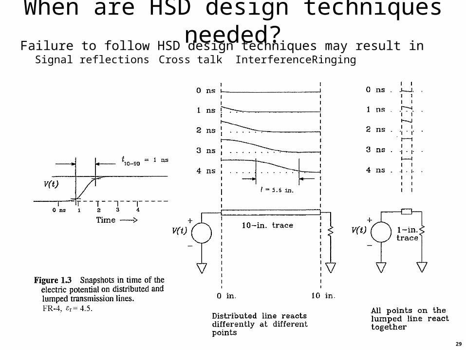
When are HSD design techniques needed?
Transient response of reactive circuits
Measuring device reactance
Impact of via inductance
Crosstalk from mutual reactance

3
SyllabusProf. Chris Allen
Ph.D. in Electrical Engineering from KU 1984
10 years industry experienceSandia National Labs, Albuquerque, NM
AlliedSignal, Kansas City Plant, Kansas City, MO
Phone: 785-864-8801
Email: [email protected]
Office: 3024 Eaton Hall
Office hours: TR: 10 to 10:50 AM
Course descriptionBasic concepts and techniques in the design and analysis of high-frequency digital and analog circuits. Topics include: transmission lines, ground and power planes, layer stacking, substrate materials, terminations, vias, component issues, clock distribution, cross-talk, filtering and decoupling, shielding, signal launching.
4
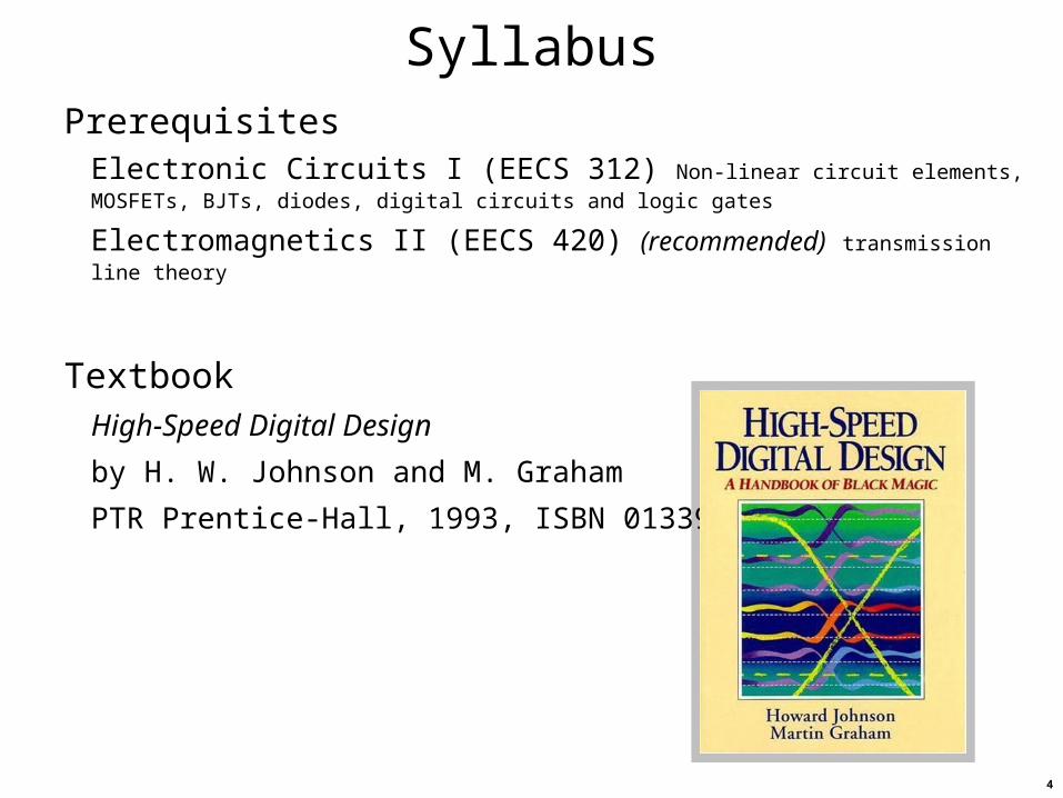
SyllabusPrerequisites
Electronic Circuits I (EECS 312) Non-linear circuit elements, MOSFETs, BJTs, diodes,
digital circuits and logic gates
Electromagnetics II (EECS 420) (recommended) transmission line theory
TextbookHigh-Speed Digital Design
by H. W. Johnson and M. Graham
PTR Prentice-Hall, 1993, ISBN 0133957241

5
Reference booksHigh-Speed Digital Propagation – Advanced Black Magicby H. W. Johnson and M. GrahamPrentice Hall PTR , 2003, ISBN 013084408X
High-Speed Digital System Design – A Handbook of Interconnect Theory and Design Practices by S. H. Hall, G. W. Hall, J. A. McCallWiley-IEEE Press, 2000, ISBN 0471360902
Digital Transmission Lines – Computer Modeling and Analysisby K. D. GranzowOxford University Press, 1998, ISBN 019511292X
Syllabus

6
Grades and course policiesThe following factors will be used to arrive at the final course grade:
Homework & quizzes 15 %Design project 15 %Midterm exam 35 %
Final exam 35 %
Grades will be assigned to the following scale:A 90 - 100 %B 80 - 89 %C 70 - 79 %D 60 - 69 %F < 60 %
These are guaranteed maximum scales and may be revised downward at the instructor's discretion.
Read the policies regarding homework, exams, ethics, and plagiarism.

7
Outline and scheduleTentative Course Outline (subject to change)
Review of circuits, electronics and traveling wave theory(Thevenin and Norton equivalents, device capacitance and inductance, current sourcing and sinking transmission line impedance, source and load impedance, reflections)
Measurement Issues(requirements and specifications, design for test, test equipment, special fixtures)
Properties of high-speed gates(circuit families and their characteristics, propagation delay, rise/fall times, input impedance, output impedance, sensitivity to electro-static discharge (ESD), heat dissipation)
Transmission lines(microstrip, stripline, coplanar, multiwire)
Ground and power planes(number of planes, placement, characteristics)
Substrate materials(printed wiring boards (PWBs), multi-chip modules (MCMs))
Thermal issues(junction temperature, thermal resistance, thermal vias, cooling options)
Packaging technologies(packaged parts on PWB (through hole and surface mount), bare die, chip-on-board, multi-chip modules)

8
Outline and scheduleTentative Course Outline (continued)
Routing issues(fanout limits, stubs, daisy chaining, testability)
Terminations and vias(termination options)
Clock distribution(timing skew, fanout, fine adjustments)
Cross-talk(analysis, design rules, consequences)
Filtering and decoupling(techniques and requirements)
Shielding and grounding(electromagnetic interference (EMI) and electromagnetic compatibility (EMC))
Signal launching(connection between boards, impedance matching)
Special high-speed circuit design techniques(pipelining and latency, multiplexing)
Future trends(chip speed, complexity, number of I/O, optical interconnection (die and board level), chip stacking)

9
OverviewMany of the topics discussed are covered adequately in the text
Other topics to be discussed will use additional resources including manufacturer’s application notes, product data sheets, and other texts.
High-frequency circuit design is both an art and a science;hence the Black Magic reference in the title.
The text presents general design rules frequently without deriving them;these result from past experience and were learned the hard way.
What is meant by high frequency or high speed?These are relative terms.What we mean is typically signals with fundamental frequency components > 100 MHz although lower frequency signals may qualify in some cases.

10
ApplicationsNumerous systems use high-speed digital signals.
Examples include:
Radar systemsGSa/s analog-to-digital converters (ADCs) and digital-to-analog converters (DACs); systems with wide signal bandwidths; computations measured in GFLOPS
Communication systemschannel rates of 40 Gb/s are common today over long-distance optical fiber
Computerssupercomputers and cluster computing; performance measured in operations per second (OPS); fine-resolution displays
Giga-sample per second: GSa/sGiga-bit per second: Gb/sGiga-floating operations per second: GFLOPS
11
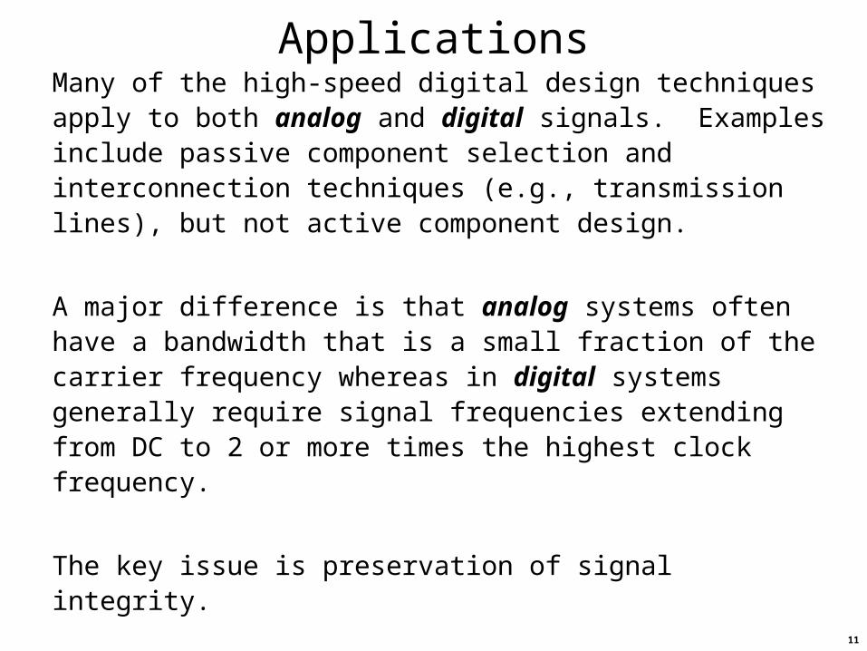
ApplicationsMany of the high-speed digital design techniques apply to both analog and digital signals. Examples include passive component selection and interconnection techniques (e.g., transmission lines), but not active component design.
A major difference is that analog systems often have a bandwidth that is a small fraction of the carrier frequency whereas in digital systems generally require signal frequencies extending from DC to 2 or more times the highest clock frequency.
The key issue is preservation of signal integrity.

12
Outline and scheduleClass Meeting Schedule
August: 25, 27September: 1, 3, 8, 10, 15, 17, 22, 24, 29October: 1, 6, 8, (no class on 13th), 15, 20, 22, 27, 29November: 3, 5, 10, 12, 17, 19, 24, (no class on 26th)December: 1, 3, 8, 10
Final exam scheduled for Wednesday, Dec 16, 10:30 a.m. to 1:00 p.m.

13
Course websiteURL: people.eecs.ku.edu/~callen/713/EECS713.htm
Contains –Syllabus
Class assignments
Some supplemental course material
Project information (when issued)
Powerpoint files used in class presentations• continually updated to correct errors or enhanced
• file contents typically span many presentations (class sessions)
• max slide count ~ 100
Links to recorded presentations (audio and Powerpoint)
Special announcements (when issued)

14
Introductions
Name
Major
Specialty
What you hope to get from of this experience(Not asking what grade you are aiming for )

15
What to expectCourse is being webcast, therefore …
Most presentation material will be in PowerPoint format Presentations will be recorded and archived (for duration of semester)
• Not 100% reliable (occasionally recordings fail due to a variety of causes)
Student interaction is encouragedRemote students must activate microphone before speaking
Please disable microphone when finished
Homework assignments will be posted on websiteElectronic homework submission logistics to be worked out
We may have guest lecturers later in the semester
To break the monotony, we’ll take a couple of 1- to 2-minute breaks during each class session (roughly every 15 to 20 min)

16
High-speed digital circuit design

17
Your first assignmentSend me an email (from the account you check most often)
Subject line: Your name – EECS 713
Tell me a little about yourself and what knowledge you hope to gain from this experience
Attach your ARTS form (or equivalent)
ARTS: Academic Requirements Tracking System
Its basically an unofficial academic record
I use this to get a sense of what academic experiences you’ve had

18
ReviewThevenin and Norton equivalent circuitsComplex circuits can be modeled in terms of
VT and ZT (Thevenin) or IN and ZN (Norton)
Note that ZT = ZN
This concept applies to both analog and digital devicesboth inputs and outputs
So we can determine the impedance (Z) of a source (driver) or a load
19
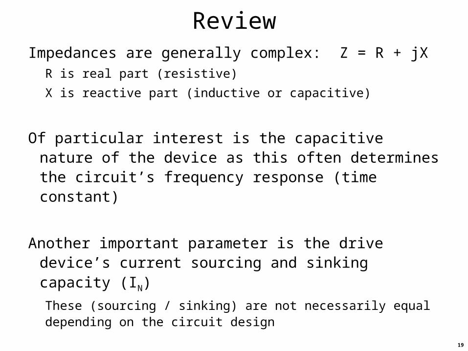
ReviewImpedances are generally complex: Z = R + jX
R is real part (resistive)
X is reactive part (inductive or capacitive)
Of particular interest is the capacitive nature of the device as this often determines the circuit’s frequency response (time constant)
Another important parameter is the drive device’s current sourcing and sinking capacity (IN)
These (sourcing / sinking) are not necessarily equal depending on the circuit design

20
ReviewTransmission lines
Characteristic impedance, Zo = V / I
Velocity of propagation, vp < c
Propagation delay, d = ℓ / vp where ℓ is the line length
Impedance mismatches between the transmission line and the source impedance (ZS) or load impedance (ZL) it connects will
reflect part of the impinging wave resulting in distortions in the voltage and current along the transmission line

21
When are HSD design techniques needed?High-speed design (HSD) techniques (to be explored later)
should be applied when the circuit trace length (the line length) ℓ is greater than about a quarter of the length of the rising edge, l
ℓ > l / 4
Where
and
propagation delay = (propagation velocity)-1
D
T
delayn propagatio
timerise rl

22
When are HSD design techniques needed?What is rise time ?
Rise time – or fall time (usually assumed to be equal) – can be defined in a variety of methodsRise time, Tr, is defined as the time required for a signal to change
from a specified low value to a specified high value.Typically these values are 10% and 90% of the step height.
Others may use 20% and 80% of the step height or the step height divided by the center or maximum slope(See Appendix B in the text for more details)

23
When are HSD design techniques needed?Why use rise time, Tr, and not the clock frequency, fCLK?
Consider the circuit
In the time domain the output signal appears as

24
When are HSD design techniques needed?
The knee frequency, Fknee, which is inversely
related to the rise time, is much higher than the clock frequency, FCLK.
rkneeCLK T2
1FF
Most energy in digital pulses concentrates below the knee frequency.Any circuit with a flat frequency response up to the Fknee frequency will pass a digital signal practically undistorted.
In the frequency domain the output signal appears as
25
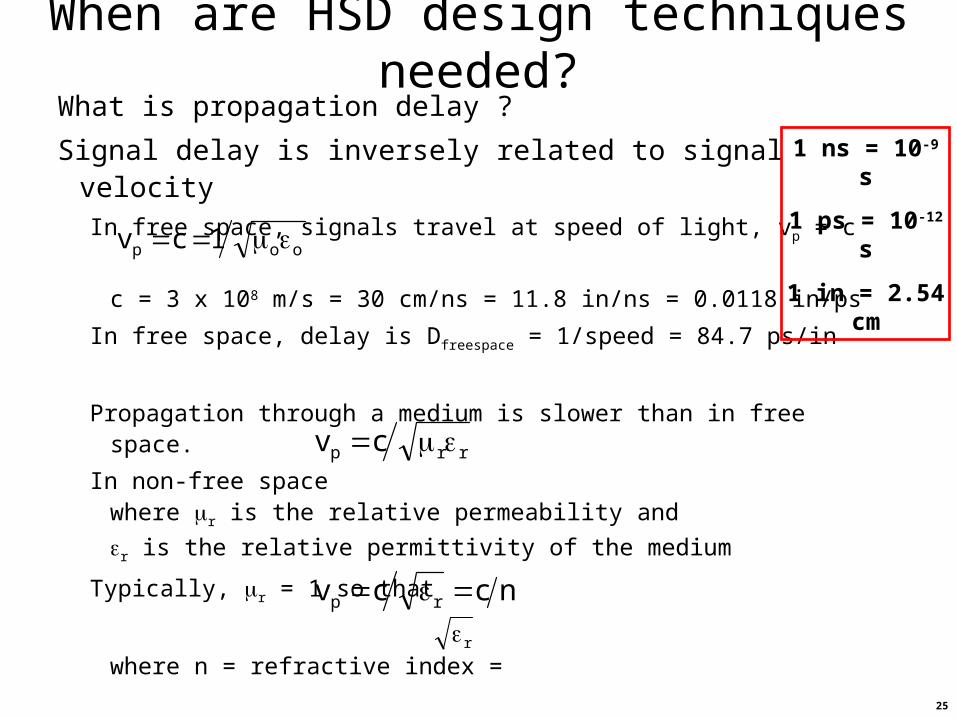
When are HSD design techniques needed?What is propagation delay ?
Signal delay is inversely related to signal velocityIn free space, signals travel at speed of light, vp = c
c = 3 x 10⁸ m/s = 30 cm/ns = 11.8 in/ns = 0.0118 in/ps
In free space, delay is Dfreespace = 1/speed = 84.7 ps/in
Propagation through a medium is slower than in free space.
In non-free spacewhere r is the relative permeability and
r is the relative permittivity of the medium
Typically, r = 1 so that
where n = refractive index =
1 ns = 10-9 s
1 ps = 10-12 s
1 in = 2.54 cmoop 1cv
rrp cv
nccv rp
r

26
When are HSD design techniques needed?What is propagation delay ?
Consider a stripline trace in FR-4 (r = 4.5, n = 2.12)
Since the field lines are confined entirely within the glass-epoxy dielectric, the propagation velocity is simply
Trace – A line or "wire" of conductive material such as copper, silver or gold, on the surface of or sandwiched inside a PCB, printed circuit board.
FR-4 – Flame-Retardant industrial laminate having a substrate of woven-glass fabric and resin binder of epoxy. FR-4 is the most common dielectric material used in the construction of PCBs in the USA
Stripline transmission line geometry
inps180D
cof47nsin565122
nsin811vp
%..
.

27
When are HSD design techniques needed?What is propagation delay ?
Now consider a microstrip trace on FR-4
Here the field lines are not confined within the glass-epoxy dielectric, so the effective permittivity is between that of air (r = 1)
and that of FR-4 (r = 4.5).
Therefore the propagation velocity is between c and 0.47c.
So for microstrip lines 85 ps/in (free space) < D < 180 ps/in (stripline).
Furthermore, the propagation velocity may be frequency dependent leading to signal dispersion and pulse distortion.
Microstrip transmission line geometry

28
When are HSD design techniques needed?What is l ?
l is the length of the rising edge and l = Tr /D.
Consider a circuit with Tr = 800 ps (GaAs technology)
Fknee for this signal will be (1600 ps)-1 or 625 MHz
The signal propagates on a stripline transmission line fabricated on alumina (r = 8.7).
Find l
So l/4 = 0.8 in or ~ 2 cmTherefore if the circuit length ℓ > 2 cm HSD design techniques should
be followed.
GaAs – An alloy of gallium and arsenic compound (GaAs) that is used as the base material for chips.
Alumina – A ceramic used for insulators in substrates in thin film circuits. It can withstand continuously high temperatures and has a low dielectric loss over a wide frequency range. Aluminum oxide (Al2O3).
cm138in23inps251
ps800in
ps25178
in
ps85D
..l
.
29
When are HSD design techniques needed?Failure to follow HSD design techniques may result in
Signal reflections Cross talk Interference Ringing

30
Transient response of reactive circuitsReactances are not usually considered in low-speed digital
circuit designs.Think about low-speed behavior as essentially DC
Reactive circuit elements of interest include:
capacitance – load, distributed, parasitic
inductance – load, distributed, parasitic
mutual capacitance – capacitive coupling
mutual inductance – inductive coupling

31
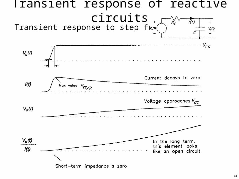
Transient response of reactive circuitsWhatever the nature of the reactance,
we can treat it as a lumped quantity being driven by a signal generator.
Consider the circuit loaded by a capacitor, driven by a step function.
Predict the resulting output voltage (Vo(t)), current (I), and short-term
impedance (i.e., Vo(t)/I(t)) as the circuit responds to the stimulus.
• What will the output voltage be immediately after the step function?
• What will be the steady-state output voltage?
• What will the current be immediately after the step function?
• What will be the steady-state current?

32
Transient response of reactive circuitsTime-domain viewpoint
Capacitor voltage cannot change instantaneously• Over short-time intervals capacitors behave as ideal voltage sources.
• For modeling purposes, capacitors are modeled as a short circuits.
Long after the transient, the capacitor current goes to zero• For modeling purposes, capacitors are modeled as open circuits.
Inductor current cannot change instantaneously• Over short-time intervals an inductor behaves as a current source.
• For modeling purposes, inductors are modeled as open circuits.
Long after the transient, the inductor voltage goes to zero• For modeling purposes, inductors are modeled as short circuits.
Frequency-domain viewpointAt high frequencies, capacitors behave as shorts, inductors as opens
At low frequencies, capacitors behave as opens, inductors as shorts
33
Transient response of reactive circuitsTransient response to step function.

34
Transient response of reactive circuitsConsider the circuit loaded by a perfect inductor,
driven by a step function.
Predict the resulting output voltage (Vo(t)), current (I), and short-
term impedance (i.e., Vo(t)/I(t)) as the circuit responds to the
stimulus.•What will the output voltage be immediately after the step function?
•What will be the steady-state output voltage?
•What will the current be immediately after the step function?
•What will be the steady-state current?

35
Transient response of reactive circuitsTransient response to step function.

36
Transient response of reactive circuitsHomework #1
Following a similar procedure, predict the transient response for the four load conditions shown.
See the course website for homework assignment details.

37
Measuring device reactanceSometimes is it necessary to measure reactance
(capacitance & inductance) of devices• circuit structures (traces)
• packages
• leaded components
Why not apply EM analysis instead ?
• too many unknowns (r, internal geometry, material )
• complex geometries, difficult to measure or model
• cost in $, time, resources
Building a small test fixture may be • more efficient and accurate
• relatively simple to fabricate

38
Measuring device reactanceTest equipment requirements
While specialized test equipment exists to characterize inductance, capacitance, resistance, etc., such instruments may not be available.
More common instrumentation that may be used include
• Pulse generator with a small Tr value
• Oscilloscope with a wide bandwidth
rdB3 T
350BW
. see page 85 in text
BW3dB – bandwidth over which signal power falls by 50% (3 dB)
Tr BW
100 ps 3.5 GHz800 ps 440 MHz
2 ns 175 MHz

39
Measuring device capacitanceCapacitance test fixture design
Simplified test circuit
Thevenin equivalent circuit connected to unknown capacitive load, Z, also known as the Device Under Test (DUT)
The output voltage from simple, first-order RC circuit is
where is the circuit’s time constant, = Rs C.
If Rs is known, the unknown capacitance, C, can be estimated by
observing the rise time of Vo
0tfore1VtV to ,
40
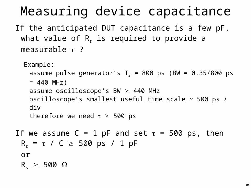
Measuring device capacitanceIf the anticipated DUT capacitance is a few pF,
what value of Rs is required to provide a measurable ?
Example:assume pulse generator’s Tr = 800 ps (BW = 0.35/800 ps = 440
MHz)assume oscilloscope’s BW 440 MHzoscilloscope’s smallest useful time scale ~ 500 ps / divtherefore we need 500 ps
If we assume C = 1 pF and set = 500 ps, thenRs = / C 500 ps / 1 pF
orRs 500

41
Measuring device capacitanceSuggested capacitance test fixture design
Determine values for R1 and R2 so that Rs 500

42
Measuring device capacitanceCapacitance test fixture design insights
To reduce reflection which would corrupt the measurement –the cables have Zo = 50 the oscilloscope has internal termination of 50 the test fixture has termination of 50 the pulse generator has source termination of 50
Coaxial cables enter/exit from opposite sides to reduce direct feed-through
R1 provides isolation between the source and the DUTR2 acts as a voltage divider with the oscilloscope’s 50- termination

43
Measuring device capacitanceSuggested value for R2 is 1000 (1 k)
This keeps the scope from loading the capacitor, i.e., without R2, Rs ~ 50
For R2 = 1000 , what should R1 be to make Rs 500 ?To answer this, analyze the circuit as seen by the DUT

44
Measuring device capacitanceThe resistance between the DUT terminals written as
Rs = (1000 + 50) // (R1 + 50 // 50) 500 or
Rs = (1050) // (25 + R1) 500 or
1/1050 + 1/(25 + R1) 1/500or
R1 930
With 5% resistorschoices are910 or 1000
ThereforeR1 = 1000
andRs = 519

45
Measuring device capacitanceWe can test our setup by shorting the DUT test points
ideal response should be zero
Circuit analysis needed topredict the range of Vo
select the power rating for resistors
using steady-state analysis when V = 1 V

46
Measuring device capacitanceIn steady state, treat DUT as open circuit
Resistance seen by sourceR = 50 + 50//2050 orR = 98.8
Source current, I1, isI1 = 1 V / 98.8 I1 = 10.1 mA
Node voltages and branch currents areVA = 1 – (50) (I1) = 494 mVI2 = 494 mV / 50 = 9.88 mAI3 = VA / 2050 = 241 AVB = (1050) (I3) = 253 mVVC = 12 mV
Note that VB/VC = 21a 21:1 voltage reduction

47
Measuring device capacitanceCapacitance test fixture design
Now find the power dissipation in various resistorsIn the pulse generator’s Rs, Pdiss = RS(I1)2 = 5 mWIn the test fixture’s 1-k resistors, Pdiss = 1k(I3)2 = 58 WIn the test fixture’s 50- resistor, Pdiss = 50(I2)2 = 5 mW
Therefore 1/8-W resistors can be used in the test fixture

48
Measuring device capacitanceCapacitance test fixture application
The Thevenin equivalent circuit for this test fixture is
With the a component in the DUT, find the rise time
when t = , Vo = Vs(1 – e-1) = 63.2% of Vs orVo = 160 mV and Vmeas = 7.58 mV
corresponds to the point where ΔV = 7.58 mVC = / 519
For example: If = 15 ns, then C = 29 pF
tso e1VV
Vmeas = Vo / 21

49
Measuring device inductanceSimilar to the discussion on capacitance measurement, we
can design a fixture for measuring device inductance.Setup designed to measure inductances as low as a few nH.
Thevenin equivalent circuit connected to unknown inductive load, Z, also known as the Device Under Test (DUT).
We know that the current through an inductor cannot change instantaneously, and
where the time constant, = L/Rs
For L = 1 nH (10-9 H) and a desired of 500 psrequires Rs ~ 2 (i.e., a small Rs value is desired)
0tfor,0
0tfor,eVtV
t
o

50
Measuring device capacitanceSuggested inductance test fixture design
Determine values for R1 and R2 so that Rs < 2

51
Measuring device capacitanceDesign requirements
• R1 + R2 = 50 at t = 0 inductance behaves as open circuit
• Rs = 50 // R2 // (R1 + 50)first 50 term represents oscilloscope terminationsecond 50 term represents pulse generator termination
Notice: There is no resistor between the DUT and the oscilloscope no voltage reduction, Vo = Vmeas
Also notice: Only R1 isolates the pulse generator from the DUT the 50- back termination is very important to manage reflections

52
Measuring device inductanceBegin by letting R1 = 39 (from author’s example)
Therefore R2 = 10 Rs = 7.6 [does not meet 2- requirement]
Voltage applied across DUT will be Vs (10//50) / (50 + 39 + 10//50) = 8.6% of Vs

53
Measuring device inductanceTry again, let R1 = 47
Therefore R2 = 2.2 Rs = 2.06 [meets 2- requirement]
Voltage applied across DUT will be Vs (2.2//50) / (50 + 47 + 2.2//50) = 2.1% of Vs

54
Measuring device inductanceNow consider the effects of testing a component with both
capacitance and inductanceExample in text describes a DUT is a 1 long trace, 0.010 (10 mils)
wide with a 0.035 (35 mils) diameter via to ground.
Estimated characteristics for this structure areC = 2 pF, L = 9 nH
At the leading pulse’s leading edge (Tr = 800 ps) the max frequency of
interest is Fknee = 0.5/Tr = 625 MHz
The capacitive reactance, Xc = (f C)-1 and for f = Fknee
Xc(f=Fknee) = Tr/( C) = 800 ps /( 2 pF) = 127 Ω
The inductice reactance, XL = 2 f L and for f = Fknee
XL(f=Fknee) = L / Tr = 9 nH / 800 ps = 35 Ω
10 mils
35 mils
11
Cross-section view of microstrip trace and via.
Oblique view of microstrip trace and via....
55
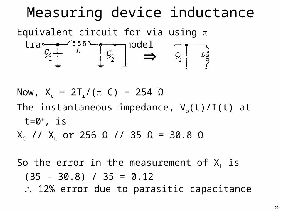
Measuring device inductanceEquivalent circuit for via using transmission line model
Now, Xc = 2Tr/( C) = 254 Ω
The instantaneous impedance, Vo(t)/I(t) at t=0+, is
XC // XL or 256 Ω // 35 Ω = 30.8 Ω
So the error in the measurement of XL is
(35 - 30.8) / 35 = 0.12 12% error due to parasitic capacitance

56
Measuring device inductanceNow find the inductance from the observed waveform
at time t1,
find time t2 on waveform so that
t2 Rs/L = 1+ t1 Rs/L
t2 – t1 = L/Rs L = Rs (t2 – t1)
LRto
seVtV
LRt11o
s1eVVtV
37.0tVeVtV 1o1
12o
1LRtLRt2o eeVeVtV s1s2

57
Measuring device inductanceThe author also presents an alternative technique for
finding L from the observed Vo(t) using the area under the
curve.
An advantage of this approach is that it is less sensitive to noise (measurement error) and less sensitive to the rise time.
A disadvantage is that it requires integration of the waveform, however this may be achieved either using built-in math functions in modern oscilloscopes orby exporting the captured the waveform for external analysis.
58
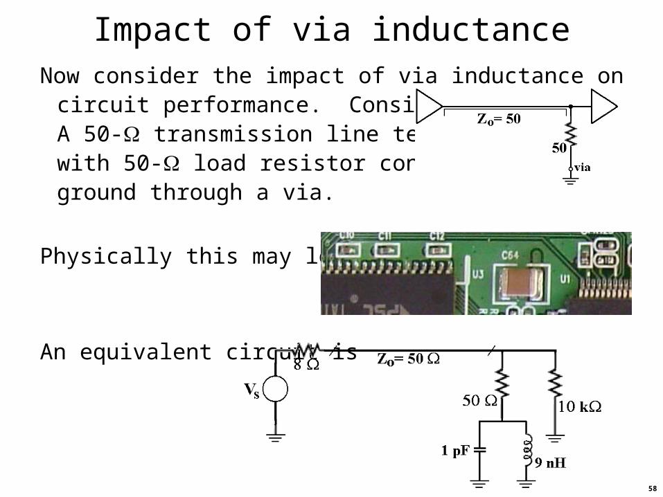
Impact of via inductanceNow consider the impact of via inductance on circuit
performance. Consider the circuitA 50- transmission line terminated with 50- load resistor connected to ground through a via.
Physically this may look like
An equivalent circuit is

59
Impact of via inductanceInstantaneous impedance at load end is
(50 + XL // XC) // 10k
where XC = Tr / ( C) and XL = L / Tr
For Tr = 3 ns, XC = 954 and XL = 9.42 , XL // XC = 9.3
The effective impedance to ground is 59 resulting impedance mismatch produces a small reflection
Reflection = (ZL – Zo) / (ZL + Zo) = 8%

60
Impact of via inductanceNow consider the impact of via
inductance on a circuit where a bus of 8 lines use a single ground via for all 8 termination resistors.
Physically this may look like
An equivalent circuit is

61
Impact of via inductanceNow the find the instantaneous impedance at load end for Tr = 3 ns. We know that XL // XC = 9.3
Consider the case when all 8 lines transition low to high
The effective transmission line impedance is 6.25 and the effective impedance to ground is 15.55 resulting a significant impedance mismatch
Reflection = (ZL – Zo) / (ZL + Zo) = (15.55 – 6.25) / (15.35 + 6.25) = 43%

62
Crosstalk from mutual reactance
Consider the circuit
In the absence of couplingthe signals A and B operateindependently, i.e., no crosstalk.
Crosstalk between circuits can occur through mutual capacitance or through mutual inductance.

63
Crosstalk from mutual capacitanceMutual capacitance involved electric field interaction between circuits A and B.
The magnitude of the mutual capacitance depends on the circuit geometry and on the material properties.
We know IM = CM dV/dt = CM d(VA-VB)/dt
Consider the case where VA = VB
static case: both high or both low and unchanging
dynamic case: both transitioning low-to-high or high-to-low
IM = 0, no capacitive current flows

64
Crosstalk from mutual capacitanceNow consider the case where VA ≠ VB
signal A transitioning from low-to-high while signal B is static low
Now dVA/dt ≈ ΔV/Tr
so IM = CM ΔV/Tr
IM represents additional current flowing in circuit B
dt
VdC
dt
Vd
dt
VdCI A
MBA
MM
0

65
Crosstalk from mutual capacitance
IM = CM ΔV/Tr flows into circuit B
VB = IM RB // RSB
if RSB >> RB, then VB = IM RB
if RSB = RB, then VB = IM RB / 2
This voltage can be thought of as crosstalk
Unwanted signal = IM RB // RSB = CM (RB // RSB) ΔV/Tr
Pure signal in B is ΔV
signalpure
signalunwantedCrosstalk
R
SBBM
T
RRCCrosstalk
//

66
Crosstalk from mutual capacitanceThe resulting crosstalkfor capacitive couplingappears as
Can we measure CM ?
For a known ΔV, Tr, RB << RSB
Integrate both sides to get
so
dt
VdCI A
MM
VCtdtd
VdCtdI M
AMM
VCRtdIRArea MBMB
BM RV
AreaC
67
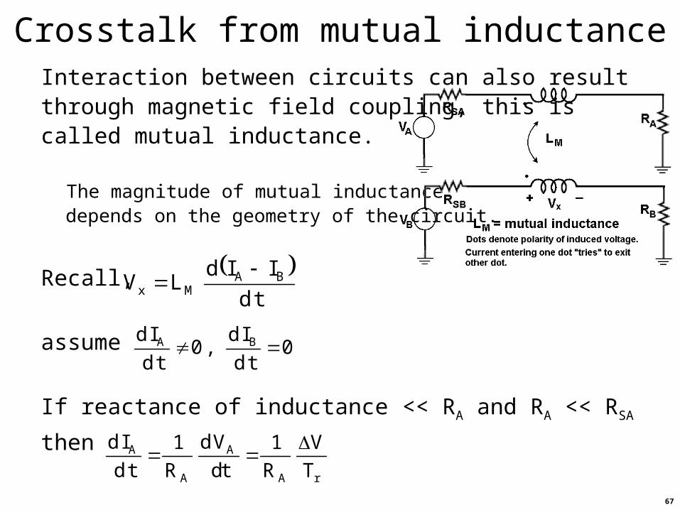
Crosstalk from mutual inductanceInteraction between circuits can also result through magnetic field coupling, this is called mutual inductance.
The magnitude of mutual inductance depends on the geometry of the circuit.
Recall,
assume
If reactance of inductance << RA and RA << RSA
then
td
IIdLV BA
Mx
0td
Id,0
td
Id BA
rA
A
A
A
T
V
R
1
td
Vd
R
1
td
Id

68
Crosstalk from mutual inductanceSo we have
Recalling our definition of crosstalk
we have
The resulting crosstalkfor inductive couplingmay appear as
The circuit geometry will determine polarity of inductive crosstalk, so polarity of signal induced into circuit B could be negative.
rAMx TR
VLV
signalpure
signalunwantedCrosstalk
rA
Mx
TR
L
V
VCrosstalk

69
Crosstalk from mutual inductanceCan we measure LM ?
For a given ΔV, Tr, RA << RSA we know
Integrate both sides to get
td
IdLV A
Mx
td
Vd
R
Ltd
td
IdLtdV
A
MAMx
A
Mx R
VLtdV
A
Mx R
VLtdVArea
so
V
RAreaL A
M
70
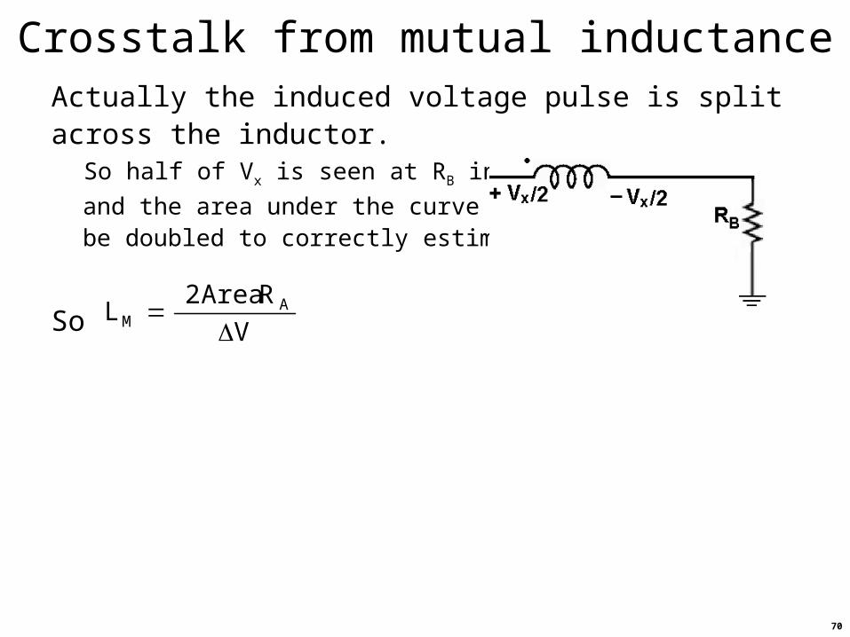
Crosstalk from mutual inductanceActually the induced voltage pulse is split across the inductor.
So half of Vx is seen at RB initially
and the area under the curve must be doubled to correctly estimate LM.
So V
RArea2L A
M

71
Crosstalk from mutual reactanceNote that the sign of Vx can be positive or negative
depending on the dot convention which depends on the circuit geometry.
Mutual inductancemay produce this
in circuit B
or this
Whereas capacitively
generated signals in B

72
Crosstalk from mutual reactanceHow to reduce crosstalk?
Recall that the source is coupled fields• electric fields capacitance• magnetic fields inductance
techniques to reduce field coupling reduced crosstalk
Examples include • increasing separation between circuits• reduce the loop area for inductive coupling• reduce the area for capacitive coupling
Other approaches• introduce isolating structures (guard traces or fence of ground vias)
• increase Tr if possible