Embed Size (px)
Citation preview

1
Evolution on JPL SABLES (Stand-Alone Board-Level Evolvable System)
A platform for fast on-chip evolutionary experiments that is essential for scaling-up the complexity of evolved HW systems.
Motivation: Develop a Evolvable Hardware systems that is• compact (handheld)• low-power • fast (seconds for complete evolution)• autonomous.
2
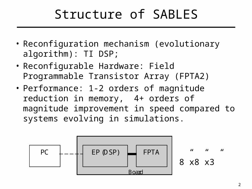
Structure of SABLES
• Reconfiguration mechanism (evolutionary algorithm): TI DSP;
• Reconfigurable Hardware: Field Programmable Transistor Array (FPTA2)
• Performance: 1-2 orders of magnitude reduction in memory, 4+ orders of magnitude improvement in speed compared to systems evolving in simulations.
FPTA
EP (DSP)
PC
Board
8”x8”x3”
3
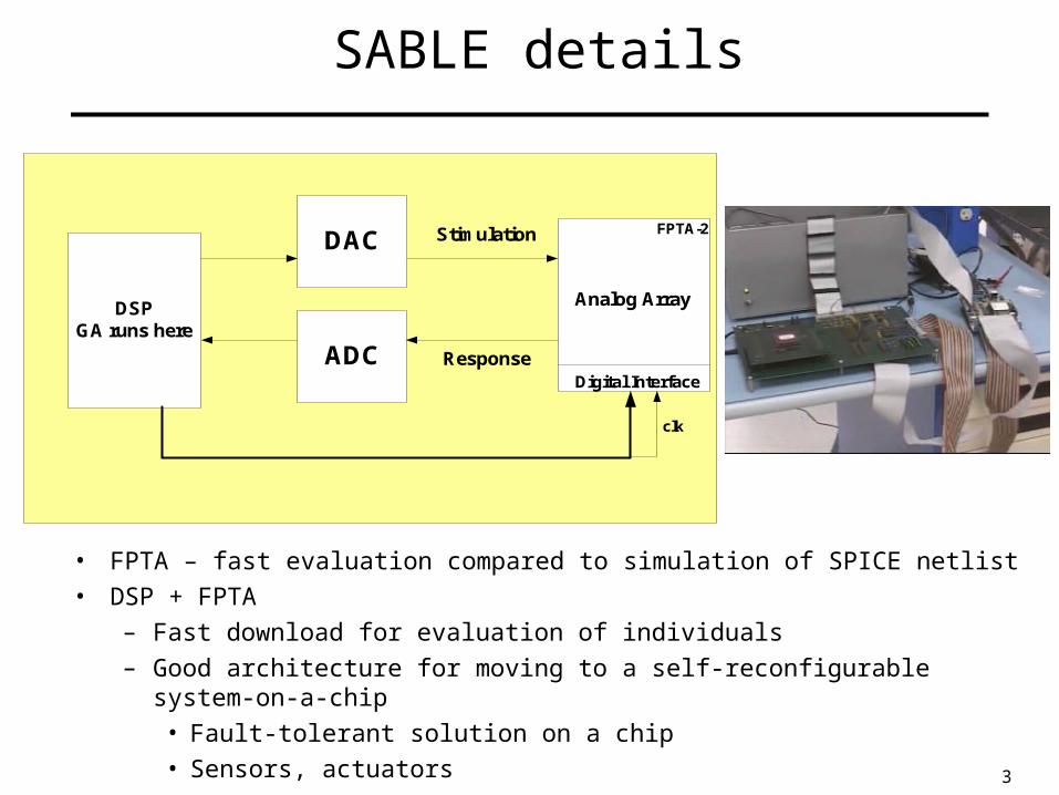
SABLE details
• FPTA – fast evaluation compared to simulation of SPICE netlist
• DSP + FPTA
– Fast download for evaluation of individuals
– Good architecture for moving to a self-reconfigurable system-on-a-chip
• Fault-tolerant solution on a chip
• Sensors, actuators
DSPGA runs here
ADC
FPTA-2
Analog Array
Digital Interface
clk
Stimulation
Response
DAC

4
SABLE architecture
Om
nib
us
In
terf
ac
e
DS
PG
A r
un
s h
ere
Servo-16
ADCs
DACs
MU
XD
EM
UX
thresholds
Interruptlogic
To DSPext int 4
FPTA-2JTAG
PC host
CodeComposer runshere - diagnostics
DIG-32
Analog Array
Digital Interface
32
DIO
32
clkTestinterface
ADDR, DATA,control
FIFO
FIFOStimulation
Response

5
Main System
• USB – JTAG emulator– Is used for downloading the EA to the DSP (2 seconds to
download)– Can be used for interaction with EA via built-in GEL functions
• Slider bars for changing variables• Graphs for displaying array contents• Works in real-time
• Innovative Integration Single Board Computer (DSP)– 160MHz, 1MB on-chip SRAM, 16MB off-chip SRAM, 32 bits of
DIO– Evaluate 1000 individuals per second– Download one cell in 50us, entire configuration in 3mS– DAC40, 40MHz 4-channel 14-bit DAC with 8kB ring-buffer– AIX20, 20MHz 4-channel 16-bit ADC
6
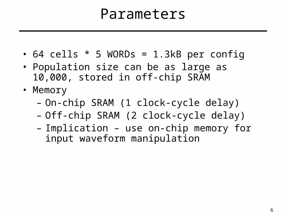
Parameters
• 64 cells * 5 WORDs = 1.3kB per config• Population size can be as large as 10,000, stored in off-
chip SRAM• Memory
– On-chip SRAM (1 clock-cycle delay)– Off-chip SRAM (2 clock-cycle delay)– Implication – use on-chip memory for input waveform
manipulation

7
FPTA Details
Chip Architecture Cell Schematic
•Technology: TSMC 0.18u•Area 5mm x 7mm;•64 cells;•Total of 256 pins;•96 analog/digital inputs •64 analog/digital outputs;•16 bits data bus/9 bits address bus control logic;•About 5000 programming bits;

8
FPTA2 - Tested Circuits
Gaussian
OpAmps
In
Out

9
2.2 - DSP
• Innovative Integration SBC167stand-alone DSP board;
• TMS320C6701processor
• 16 analog inputs and outputs at 100 kSamples;
• 32 Digital I/O at 7.5MHz.
• Fits in a box 8” x 8” x 3”.

NIECE – Novel Interface for an Evolutionary Computing Environment
Features: • Fully graphical user interface• Ability to control all evolutionary parameters• Java/C Hybrid – fully portable, optimized for speed• Compressed storage of an entire evolutionary experiment offline• Batch Mode functionality• Several Data Views• Compatible with an evolutionary systems with infinite generations, population size, inputs, responses, chromosome size• USB Interface with SABLE
Overview: Graphical User Interface for Visualization of Evolutionary Experiments
Goals: • Provide a customizable data acquisition protocol to selectively collect data• View evolution in several ways, online and offline• Save data in a compressed format• Interface with any evolutionary system

11
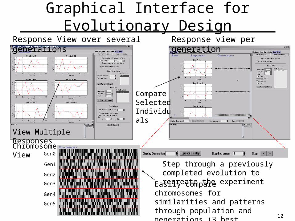
Graphical Interface for Evolutionary Design
Specify All GA Parameters at
runtime
Several possible acquisition protocols
Collect data only from user specified generations
Collect only user specified individuals
(from and to specified ranks, with a stride)
Collect only user specified data
vectors
Parameters can be different per
generation and changed on the fly
User specified fitness function for
compilation
GA Parameters Data Acquisition
12
Graphical Interface for Evolutionary DesignResponse View over several generations Response view per generation
Chromosome View
Easily compare chromosomes for similarities and patterns through population and generations (3 best individuals over 6 generations)
Step through a previously completed evolution to recreate the experiment
Compare Selected Individuals
View Multiple Responses
Gen0
Gen1
Gen2
Gen3
Gen4
Gen5

Data Acquisition From SABLE
USB Protocol provides rapid data acquisition (300KBps)
DSPGA runs here
ADC
FPTA-2
Analog Array
Digital Interface
clk
Stimulation
Response
DAC
SABLE
USB
NIECE
Command Packets
• Transmit all GA parameters (mutation, crossover, etc)• 32byte packets• Communicate customized acquisition settings – significantly reduces debugging and analysis time• Change & control evolution on the fly
Data Packets
• Send back compressed data• 64byte packets
Configuration bits GA Parameters Acquisition Parameters
32 bytes
Configuration bits Fitness values Chromosomes Responses Other Data
64 bytes

14
Evolution on SABLES
Evolutionary Algorithm
Assessfitness
Specs.
Chromosomes1011001101010001
Configurationbitstrings
Responses
Candidate configurations are tested on-chip; the best ones are modified by the evolutionary algorithm in a guided search for solutions.
Evolutionary Processor (EP) in DSPReconfigurable HardwareField Prog.Transistor Array (FPTA)
FPTAEP (DSP)
Information flow and implementation with DSP/FPTA chip pair
SABLES
Speed. Portability. Stand-alone. Autonomy?
15
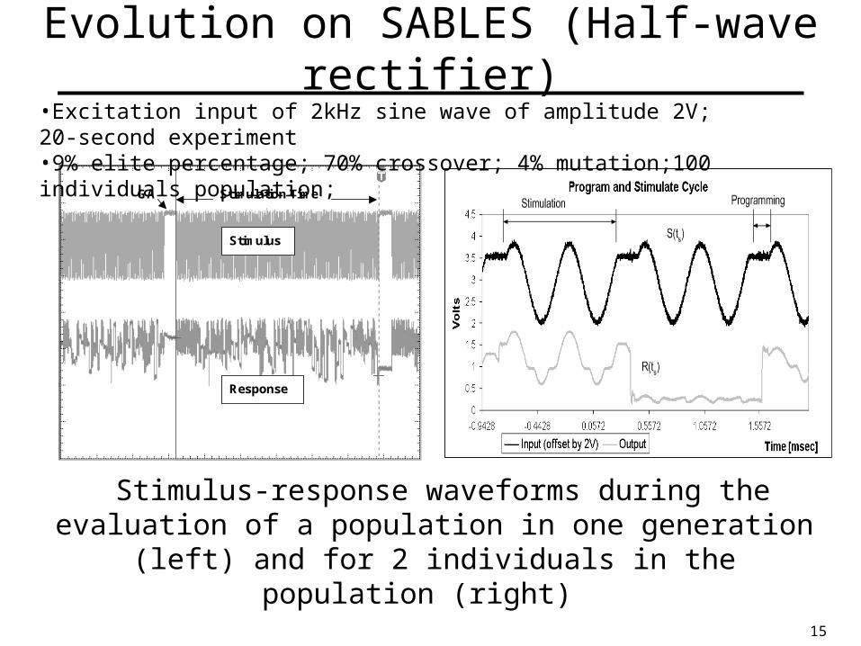
Evolution on SABLES (Half-wave rectifier)
Stimulation Time GA
Stimulus
Response
Stimulus-response waveforms during the evaluation of a population in one generation (left) and for 2 individuals in the population
(right)
•Excitation input of 2kHz sine wave of amplitude 2V; 20-second experiment•9% elite percentage; 70% crossover; 4% mutation;100 individuals population;

16
Half-wave rectifier evolution waveforms
a) b)
c) d)
Solution at generation 82 (after 8200 circuits evaluated in ~8s)
Best individual of generation a) 1, b) 5, c) 50 d) 82

17
Half-wave rectifier fitness progress
The fitness function as generations progress.

18
Self-configuration for functional change
When a function is specified the hardware evolves/self-configures to a circuit satisfying the requirements; when mission/requirements change, the same hardware changes again subject to a new evolutionary search
Analog multiplier
Requirement A Requirement B
Digital multiplexer
Percentage of satisfaction of requirement 100%
0%
Function 1 Function 2
time

19
Other evolved circuits
3-bit DAC 4-bit DACAutomatic Gain Control
response
Oscillators
In2
Out1
Out2
In1
Signal Separators High-Pass Filters
In
Out
In
Out
Out
In

20
Evolution on SABLES (Tunable Filters)
• Tunable filter circuit circuit• Excitation input:
– e1 = Asin(2f1) + Bsin (2f2)– A and B unknown
• Objective: Amplify more powerful frequency component, attenuate the weakest (pass A if A>B, else pass B).
• 9% elite percentage; • 70% crossover;• 4% mutation;• 400 individuals population;• 60 seconds experiments

21
Evolution on SABLES (Tunable Filters)
Frequency(Hz)
FFT
(Intp
ut S
igna
l)
0 15,000 30,000 45,0000612182430364248
Frequency (Hz)
FFT
Inpu
t Sig
nal
0 15,000 30,000 45,000048121620242832
Filter characteristic:•10kHz : -2.86dB attenuation•20kHz : -15.8dB attenuation
Filter characteristic:•10kHz : -12.5dB attenuation•20kHz : -4.8dB attenuation
Input
Output
Input
Output
Frequency(Hz)
FFT
(Out
put S
igna
l)
0 15,000 30,000 45,0000
2.5
5
7.5
10
12.5
15
17.5
Frequency(Hz)
FFT
(Out
put S
igna
l)
0 15,000 30,000 45,0000246810121416
Signal/Noise = 4.1dB
Signal/Noise = 16.9dB
Signal/Noise = 10.8dB
Signal/Noise = 18.5dB

22
On certain traps of evolutionary engineering
• Problems related to the formulation of requirements: facilitate translation of target specifications into the language of evolution, including representations, fitness function and parameters of the algorithm.
• Autonomous systems: provide complete up-front specifications;
• Two identified traps:
– Transient solutions;
– Operational Range in the frequency domain;
– Time constants
23
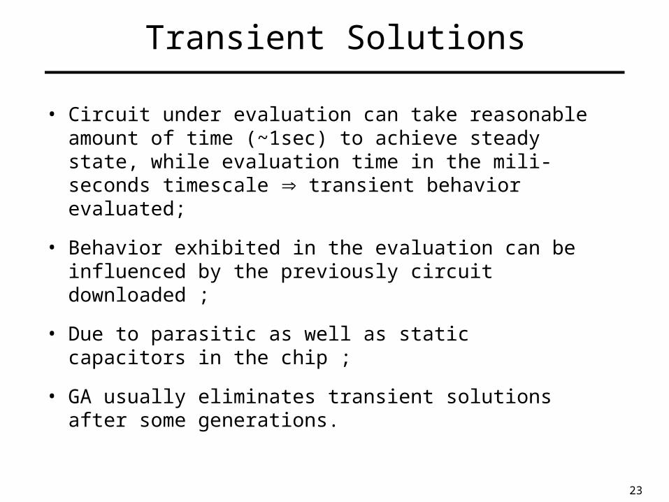
Transient Solutions
• Circuit under evaluation can take reasonable amount of time (~1sec) to achieve steady state, while evaluation time in the mili-seconds timescale transient behavior evaluated;
• Behavior exhibited in the evaluation can be influenced by the previously circuit downloaded ;
• Due to parasitic as well as static capacitors in the chip ;
• GA usually eliminates transient solutions after some generations.

24
An example of transient behavior. The degradation shown from a) to d) occurred over the span of approximately 1 second.
Illustration of Transient Behavior
a) b)
c) d)

25
Operational Range in the Frequency Domain
Response of the half-wave rectifier for a frequency sweep from 500Hz to 5kHz (left).
Deteriorated response at 50kHz.
•Circuit evolved at 2kHz does not work at more than 10kHz
• Circuit behavior should be evaluated for the overall frequency domain in which it is expected to work

26
Effect of Timescales
• Evolutionary design requires explicit formulation of assumptions often implicit to human designers;
• Example: evolved logic gates often present different behavior over a "frequency range" i.e. function with slow/DC signals as well as to faster input changing signals.– Evolution in small timescales: transient solutions;– Evolution in large timescales: slow gates;
• Solutions:– Mixtrinsic evolution: using combined simulation models;– Increase transient analysis duration to ‘catch’ operating point;– Decrease step of transient analysis: check circuit behavior after transition;– Increase output load to ensure a fast gate.

27
Time Constants
Time (Micro-seconds)
Inpu
t1(V
olts
)
0 2.5 5 7.5 100
1
2
3
4
Time (Micro-seconds)
Inpu
2(Vo
lts)
0 2.5 5 7.5 100
1
2
3
4
Time (micro-seconds)
Out
put (
Volts
)
0 2.5 5 7.5 100
1
2
3
4
Time (Seconds)
Inpu
t1 (V
olts
)
0 25 50 75 1000
1
2
3
4
Time (Seconds)
Inpu
t2 (V
olts
)
0 25 50 75 1000
1
2
3
4
Time (Seconds)
Out
put (
Volts
)
0 25 50 75 1000
1
2
3
4
Time (Micro-seconds)
Inpu
t1(V
olts
)
0 2.5 5 7.5 100
1
2
3
4
Time (Micro-seconds)
Inpu
2(Vo
lts)
0 2.5 5 7.5 100
1
2
3
4Time (Seconds)
Inpu
t1 (V
olts
)
0 25 50 75 1000
1
2
3
4
Time (Seconds)
Inpu
t2 (V
olts
)
0 25 50 75 1000
1
2
3
4
Time (Micro-seconds)
Out
put (
Volts
)
0 2.5 5 7.5 100
1
2
3
4
Time (Seconds)
Out
put (
Volts
)
0 25 50 75 1000
1
2
3
4
Evolved NAND gate evaluated inthe timescale of microsecond (until 10-5 sec)
microsecond second microsecond second
Evolved NAND gate using two different timescales
Evolutionin simulation