Embed Size (px)
Citation preview
University of Tennessee, Knoxville University of Tennessee, Knoxville
TRACE: Tennessee Research and Creative TRACE: Tennessee Research and Creative
Exchange Exchange
Doctoral Dissertations Graduate School
8-2007
Intrinsically Evolvable Artificial Neural Networks Intrinsically Evolvable Artificial Neural Networks
Saumil Girish Merchant University of Tennessee - Knoxville
Follow this and additional works at: https://trace.tennessee.edu/utk_graddiss
Part of the Electrical and Computer Engineering Commons
Recommended Citation Recommended Citation Merchant, Saumil Girish, "Intrinsically Evolvable Artificial Neural Networks. " PhD diss., University of Tennessee, 2007. https://trace.tennessee.edu/utk_graddiss/244
This Dissertation is brought to you for free and open access by the Graduate School at TRACE: Tennessee Research and Creative Exchange. It has been accepted for inclusion in Doctoral Dissertations by an authorized administrator of TRACE: Tennessee Research and Creative Exchange. For more information, please contact [email protected].

To the Graduate Council:
I am submitting herewith a dissertation written by Saumil Girish Merchant entitled "Intrinsically
Evolvable Artificial Neural Networks." I have examined the final electronic copy of this
dissertation for form and content and recommend that it be accepted in partial fulfillment of the
requirements for the degree of Doctor of Philosophy, with a major in Electrical Engineering.
Gregory D. Peterson, Major Professor
We have read this dissertation and recommend its acceptance:
Donald W. Bouldin, Itamar Elhanany, Ethan Farquhar, J. Wesley Hines
Accepted for the Council:
Carolyn R. Hodges
Vice Provost and Dean of the Graduate School
(Original signatures are on file with official student records.)

To the Graduate Council: I am submitting herewith a dissertation written by Saumil Girish Merchant entitled “Intrinsically Evolvable Artificial Neural Networks.” I have examined the final electronic copy of this dissertation for form and content and recommend that it be accepted in partial fulfillment of the requirements for the degree of Doctor of Philosophy, with a major in Electrical Engineering.
Gregory D. Peterson, Major Professor
We have read this dissertation and recommend its acceptance: Donald W. Bouldin Itamar Elhanany Ethan Farquhar J. Wesley Hines
Accepted for the Council:
Carolyn R. Hodges
Vice Provost and Dean of the Graduate School
(Original signatures are on file with official student records.)
INTRINSICALLY EVOLVABLE
ARTIFICIAL NEURAL NETWORKS
A Dissertation Presented for the Doctor of Philosophy
Degree The University of Tennessee, Knoxville
Saumil Merchant August 2007

ii
DEDICATION
This dissertation is dedicated to my wife, Jaya
for her love and support and
to my parents, Kokila and Girish Merchant
for their love and encouragement.

iii
Copyright © 2007 by Saumil Merchant
All rights reserved.

iv
ACKNOWLEDGEMENTS
I have been fortunate to have so many people in my life who have been a part of
my graduate education and without them this dissertation wouldn't have been possible. I
am what I am today because of all these people.
First and foremost, I would like to thank my advisor and teacher, Dr. Gregory
Peterson. I couldn't have wished for a better mentor who was always able to help me see
the bigger picture and create a vision for this dissertation. His faith in me has inspired me,
and his patience and constructive criticisms have guided me. Throughout this journey he
has been a friend and a mentor with my best interest in his mind. He has molded an
aspiring student from a novice to a researcher.
I would also like to express my sincere thanks to Dr. Seong Kong for his
guidance, Dr. Donald Bouldin for his teachings on VLSI systems and serving on my
committee. I would also like to express my heartfelt gratitude to Dr. Itamar Elhanany, Dr.
Wesley Hines, and Dr. Ethan Farquhar for serving on my dissertation committee.
I would like to thank my friends and lab mates, Junqing Sun, Akila
Gothandaraman, Yu Bi, Junkyu Lee, Depeng Yang, Sang Ki Park, and Wei Jiang for
their valuable feedback at various times during this work. I would also like to take this
opportunity to thank all my friends in Knoxville who were always there for me at times I
felt I would be losing my sanity.

v
I would like to acknowledge and appreciate the financial support provided for this
research work and my graduate studies by the Electrical and Computer Engineering
Department at University of Tennessee, the National Science Foundation, and the Office
of Information Technology – Lab Services.
I owe special gratitude to my parents, Kokila and Girish Merchant, who always
kept faith in me, and offered unconditional support and encouragement; to my aunt and
uncle, Jayshree and Sanjay Merchant for inspiration and the needed push; my sister
Snehal Merchant and cousin Rahil Merchant for their support and encouragement; my
niece Shweta Merchant for her affection; and my mother and father-in-law Usha and
Suresh Bajaj for their trust. Thank you!
Last but not the least; I thank my best friend and wife Jaya for her enduring
patience, love, and support through these years. She is the one responsible to inspire me
to pursue doctoral studies. Her love has been my strength, and her faith my inspiration.
vi
ABSTRACT
Dedicated hardware implementations of neural networks promise to provide
faster, lower power operation when compared to software implementations executing on
processors. Unfortunately, most custom hardware implementations do not support
intrinsic training of these networks on-chip. The training is typically done using offline
software simulations and the obtained network is synthesized and targeted to the
hardware offline. The FPGA design presented here facilitates on-chip intrinsic training of
artificial neural networks. Block-based neural networks (BbNN), the type of artificial
neural networks implemented here, are grid-based networks neuron blocks. These
networks are trained using genetic algorithms to simultaneously optimize the network
structure and the internal synaptic parameters. The design supports online structure and
parameter updates, and is an intrinsically evolvable BbNN platform supporting
functional-level hardware evolution. Functional-level evolvable hardware (EHW) uses
evolutionary algorithms to evolve interconnections and internal parameters of functional
modules in reconfigurable computing systems such as FPGAs. Functional modules can
be any hardware modules such as multipliers, adders, and trigonometric functions. In the
implementation presented, the functional module is a neuron block. The designed
platform is suitable for applications in dynamic environments, and can be adapted and
retrained online. The online training capability has been demonstrated using a case study.
A performance characterization model for RC implementations of BbNNs has also been
presented.
vii
TABLE OF CONTENTS
Chapter Page 1 Introduction................................................................................................................... 1
1.1 Technology Overview: RC, EHW, and ANN......................................................... 1 1.1.1 RC Acceleration for ANNs............................................................................... 5
1.2 Dissertation Synopsis.............................................................................................. 6 1.3 Manuscript Organization ........................................................................................ 9
2 Artificial Neural Networks ......................................................................................... 11 2.1 Introduction to Artificial Neural Networks........................................................... 11 2.2 Historical Perspective ........................................................................................... 14 2.3 Building Artificial Neural Networks .................................................................... 15 2.4 Genetic Evolution of Artificial Neural Networks................................................. 17 2.5 Review of Neural Hardware Implementations ..................................................... 19
2.5.1 Neural Network Hardware.............................................................................. 19 2.5.2 Digital Neural Network Implementations....................................................... 21 2.5.3 Analog Neural Hardware Implementations .................................................... 35 2.5.4 Hybrid Neural Hardware Implementations..................................................... 36
2.6 Summary ............................................................................................................... 37 3 Evolvable Hardware Systems ..................................................................................... 39
3.1 Gate-level, Transistor-level, and Functional-level Evolution............................... 40 3.2 Review of Evolvable Hardware Systems.............................................................. 42
3.2.1 EHW Chips and Applications......................................................................... 44 3.2.2 EHW Algorithms and Platforms..................................................................... 49
3.3 Summary ............................................................................................................... 51 4 Block-based Neural Networks .................................................................................... 53
4.1 Introduction........................................................................................................... 53 4.2 Evolving BbNNs Using Genetic Algorithms........................................................ 56
4.2.1 Genetic Operators ........................................................................................... 59 4.2.2 BbNN Encoding.............................................................................................. 61 4.2.3 Fitness Function.............................................................................................. 64 4.2.4 Genetic Evolution ........................................................................................... 65
4.3 Summary ............................................................................................................... 68 5 Intrinsically Evolvable BbNN Platform...................................................................... 70
5.1 BbNN FPGA Design Details ................................................................................ 70 5.1.1 Data Representation and Precision ................................................................. 73 5.1.2 Activation Function Implementation .............................................................. 74 5.1.3 Smart Block-based Neuron Design................................................................. 76 5.1.4 Dataflow Implementation ............................................................................... 81
5.2 Embedded Intrinsically Evolvable Platform......................................................... 86 5.2.1 PSoC Platform Design .................................................................................... 88
5.3 Fixed Point BbNN Software for Genetic Evolution ............................................. 91 5.4 Performance and Device Utilization Summary .................................................... 92 5.5 Design Scalability ................................................................................................. 93
5.5.1 Scaling BbNN Across Multiple FPGAs ......................................................... 96
viii
5.5.2 Scaling via Time Folding................................................................................ 96 5.5.3 Hybrid Implementation................................................................................... 97
5.6 Applications .......................................................................................................... 97 5.6.1 N-bit Parity Classifier ..................................................................................... 97 5.6.2 Iris Plant Classification................................................................................. 102
5.7 Summary ............................................................................................................. 107 6 Online Learning With BbNNs .................................................................................. 109
6.1 Online Training Approach .................................................................................. 110 6.2 Online Evolution of BbNNs................................................................................ 115 6.3 Case Study: Adaptive Neural Luminosity Controller......................................... 118
6.3.1 Simulation Experimental Setup .................................................................... 120 6.3.2 Adaptive BbNN Predictor............................................................................. 124
6.4 Summary ............................................................................................................. 156 7 Performance Analysis ............................................................................................... 157
7.1 Computational Device Space.............................................................................. 157 7.2 RP Space ............................................................................................................. 159 7.3 Performance Characterization Metrics ............................................................... 162
7.3.1 Computational Device Capacity ................................................................... 163 7.3.2 Computational Density ................................................................................. 165 7.3.3 Power Efficiency........................................................................................... 166 7.3.4 Discussion..................................................................................................... 167
7.4 BbNN Performance Analysis.............................................................................. 168 7.4.1 Performance Characterization on Processors................................................ 169 7.4.2 Performance Characterization on FPGAs..................................................... 172 7.4.3 Results and Discussion ................................................................................. 177 7.4.4 Performance of SBbNs ................................................................................. 186
7.5 Model Sensitivity to Parametric Variations........................................................ 187 7.6 Summary ............................................................................................................. 190
8 Summary and Conclusions ....................................................................................... 191 References....................................................................................................................... 198 Appendix......................................................................................................................... 214 Vita.................................................................................................................................. 218
ix
LIST OF TABLES
Table 1 Typical FPGA runtime reconfiguration times .................................................... 29 Table 2 Device Utilization Summary on Xilinx Virtex-II Pro FPGA (XC2VP30)......... 94 Table 3 Device Utilization Summary on Xilinx Virtex-II Pro FPGA (XC2VP70)......... 95 Table 4 Genetic evolution parameters used for N-bit Parity problem ............................ 98 Table 5 Genetic evolution parameters used for Iris classification problem................... 104 Table 6 Light and sensor specifications for the test room ............................................. 123 Table 7 Genetic evolution parameters used for BbNN predictor .................................. 127 Table 8 GA evolution parameters used for BbNN controller ........................................ 140 Table 9 Re-train cycle times .......................................................................................... 147 Table 10 Peak Computational Capcity (in MCPS) and density (in CPλ2S) of RISC processors for BbNN block computation........................................................................ 171 Table 11 BbNN Computational Density on FPGAs..................................................... 176
x
LIST OF FIGURES
Figure 1 Venn diagram showing the technology overlaps between RC, EHW, and ANN 6 Figure 2 (a) Block-based neural network topology (b) 2 input / 2 output neuron block configuration ....................................................................................................................... 8 Figure 3 Mathematical model of an artificial neuron ...................................................... 11 Figure 4 (a) Non-recurrent multilayer perceptron network (b) Recurrent artificial neural network ............................................................................................................................. 12 Figure 5 Multilayer Perception Example (a) Training Iteration ‘n’ (b) Training iteration ‘n+1’.................................................................................................................................. 17 Figure 6 Neural network hardware classification ............................................................ 21 Figure 7 Block-based Neural Network topology............................................................. 54 Figure 8 Four different internal configurations of a basic neuron block ......................... 54 Figure 9 Three different 2 x 2 BbNN network structures................................................ 56 Figure 10 Flowchart depicting genetic evolution process ............................................... 58 Figure 11 Recurrent BbNN network structure encoding (a) BbNN (b) Structure encoding........................................................................................................................................... 62 Figure 12 Feedforward BbNN network structure encoding (a) BbNN (b) Structure encoding............................................................................................................................ 62 Figure 13 BbNN weight gene encoding (a) Neuron block (b) Weight encoding ............ 63 Figure 14 BbNN chromosome encoding for a 2 x 2 network.......................................... 63 Figure 15 Structure crossover operation in BbNN .......................................................... 66 Figure 16 Structure mutaiton operation in BbNN............................................................ 67 Figure 17 Activation function LUT illustration............................................................... 76 Figure 18 Smart Block-based Neuron to emulate all internal neuron block configurations........................................................................................................................................... 78 Figure 19 Bit fields of Block Control and Status Register (BCSR) of SBbN ................. 79 Figure 20 Dynamic gene translation logic for internal configuration emulation............. 80 Figure 21 Equivalent Petri Net models for BbNN blocks (a) 1/3 (b) 2/2 (c) 3/1 ........... 83 Figure 22 An example 2 x 2 BbNN firing sequence........................................................ 84 Figure 23 SBbN neuron logical block diagram ............................................................... 85 Figure 24 Programmable System on a Chip - logical diagram........................................ 90 Figure 25 BbNN PSoC platform. GA operators execute on PPC405,............................. 91 Figure 26 Fitness evolution trends for (a) 3-bit and (b) 4-bit parity examples............... 99 Figure 27 Structure evolution trends for (a) 3-bit and (b) 4-bit parity examples .......... 100 Figure 28 Evolved networks for (a) 3-bit and (b) 4-bit parity examples ...................... 101 Figure 29 BbNN training error for Iris plant classification database. Results show ..... 104 Figure 30 Fitness trends was Iris plant classification using BbNN ............................... 105 Figure 31 Structure evolution trends for Iris plant classification using BbNN ............. 105 Figure 32 Evolved BbNN network for Iris plant classification database ...................... 106 Figure 33 Single network scheduled to switch between training and active modes...... 111 Figure 34 Two networks scenario. One in active mode and the other in training mode 113 Figure 35 Online training system model........................................................................ 115 Figure 36 Time delayed neural network ........................................................................ 117 Figure 37 Layout of the reference room used for simulation ........................................ 121
xi
Figure 38 Plot of measured relative light output (%) versus ballast control input ........ 122 Figure 39 Plot of sensor signal output (V) versus measured light intensity .................. 122 Figure 40 Ideal luminosity levels in the test room......................................................... 125 Figure 41 Results of the BbNN pre-training. Plot shows the actual and the predicted ambient luminosity values as learnt by BbNN ............................................................... 126 Figure 42 Prediction error for the offline evolution....................................................... 126 Figure 43 Avergae and maximum fitness values over generations (offline evolution). 127 Figure 44 Evolved BbNN after 1557 generations.......................................................... 128 Figure 45 Ambient luminosity test cases and expected target luminosity..................... 129 Figure 46 Pre-trained ambient luminosity predictions and the current ambient luminosity......................................................................................................................................... 131 Figure 47 Predictions improve after first re-training cycle at 8:00................................ 131 Figure 48 Predictions improve after the second re-training cycle at 17:50 ................... 132 Figure 49 Prediction errors for pre-trained, first re-training, and second re-training cycles............................................................................................................................... 132 Figure 50 Average and maximum fitness trends for the first re-training cycle ............. 133 Figure 51 Average and maximum fitness trends for the second re-training cycle ........ 133 Figure 52 Evolved network after the first re-training cycle........................................... 134 Figure 53 Evolved network after the second re-training cycle ...................................... 135 Figure 54 BbNN predictor - controller block diagram .................................................. 140 Figure 55 Target and measured luminosity levels as recorded by the........................... 141 Figure 56 Error between target and measured luminosities (pre-trained case) ............. 141 Figure 57 Target and measured luminosity levels as recorded by the........................... 142 Figure 58 Error between target and measured luminosities (online evolution case)..... 142 Figure 59 Power consumption (pre-trained case) .......................................................... 143 Figure 60 Power consumption (online evolution case).................................................. 143 Figure 61 BbNN controller at time - 4:00hrs. (a) Fitness Curves (b) Evolved BbNN .. 145 Figure 62 Actual and pre-trained predictions of ambient light intensity ....................... 147 Figure 63 Actual and predicted ambient light intensity values throughout the course.. 148 Figure 64 Prediction errors of all the re-training steps. The errors curves show the..... 149 Figure 65 The plot shows the prediction errors for the eighth re-training cycle and..... 150 Figure 66 Fitness curves for the evolves BbNN eighth re-training cycle...................... 150 Figure 67 Evolved BbNN network after eighth re-training cycle.................................. 151 Figure 68 Target and measured luminosity reading for the sunnydataset - pre-trained case.................................................................................................................................. 153 Figure 69 Luminosity error for the sunny dataset - pre-trained case............................. 153 Figure 70 Target and measured luminosity readings for the sunny dataset................... 154 Figure 71 Luminosity error for the sunny case with all eight re-training cycles........... 154 Figure 72 Total power consumption for sunny case - pre-trained case ......................... 155 Figure 73 Total power consumption with sunny dataset - eight re-training cycles ...... 155 Figure 74 Reorganization of the VP space with advances in RP device technologies .. 162 Figure 75 RISC assembly code for a single neuron processing..................................... 169 Figure 76 Pipelined multiplier accumulator circuit for neural processing .................... 173 Figure 77 Pipelined parallel multiplier circuit for neural processing ............................ 173 Figure 78 Comparing processors and FPGAs (Hard MAC) (a) Capacity (b) Density .. 178

xii
Figure 79 Comparing processors and FPGAs (LUT MAC) (a) Capacity (b) Density .. 179 Figure 80 Comparing processors and FPGAs (Hard Multipliers) (a) Capacity (b) Density......................................................................................................................................... 180 Figure 81 Comparing processors and FPGAs (LUT Multipliers) (a) Capacity (b) Density......................................................................................................................................... 181 Figure 82 Comparing power efficiencies of processors and FPGAs (Hard MAC) ....... 182 Figure 83 Comparing power efficiencies of processors and FPGAs (LUT MAC) ....... 182 Figure 84 Comparing power efficiencies of processors and FPGAs (Hard Multiplier) 183 Figure 85 Comparing power efficiencies of processors and FPGAs (LUT Multiplier) 183 Figure 86 Computational capacities of FPGAs and processors as a function of network size .................................................................................................................................. 185 Figure 87 Deviation in computational density verses die area deviation factor ............ 189
1 INTRODUCTION
1.1 Technology Overview: RC, EHW, and ANN
Reconfigurable computing (RC) technology has grown considerably in the past
two decades and continues to arouse much interest among the computing community.
Performance advantages of dedicated custom/semi-custom implementations, shorter
design and verification times, device reusability, and lower implementation costs as
compared to application specific integrated circuits (ASIC) have been the major
contributing factors in the success of this technology. The most prominent and
commercially successful device in this technology is the field programmable gate array
(FPGA). Increasing speeds and capacities, availability of on-chip cores such as embedded
processors, memories, multipliers, and accumulators, and functional diversity advantages
with runtime reconfiguration make FPGAs very attractive low-volume and low-cost
custom hardware solutions. Increasing commercial acceptance has promoted significant
research in CAD tools to efficiently program these devices and a huge market for
intellectual property cores to facilitate shorter design cycles. Broad application range,
from embedded computing to supercomputing, continues to stimulate research into this
technology [1].
The runtime reconfiguration capability of RC devices has resulted in the
conception of a different computing paradigm among a small community of researchers.
The computing paradigm is Evolvable hardware (EHW) [2]. The key objective of EHW
1
2
systems is to use the runtime hardware reconfiguration ability along with evolutionary
algorithms to evolve a digital or analog circuit in hardware. The configuration bitstream
(viewed as a phenotype in an evolutionary algorithm) of these devices is encoded as a
chromosome (viewed as a genotype) and evolved under the control of evolutionary
algorithms over multiple generations. Evolutionary algorithms use mechanisms inspired
by the Darwinian theory of biological evolution such as reproduction, mutation,
recombination, natural selection, and survival of the fittest to evolve a population of
chromosomes over multiple generations. A population of chromosomes (encoded FPGA
bitstreams) is first ranked according to their fitness levels. Fitness is determined by an
objective function that can include parameters such as correctness of circuit functionality,
speed, area, and power. A selection scheme selects the chromosomes from the population
for reproduction via genetic crossover, mutation, and recombination. The higher the rank,
the higher is the probability of selection of the chromosomes for reproduction to form
new generations. The survival of the fittest policy tends to increase the average fitness of
the population over multiple generations. Evolution continues over multiple generations
until either a chromosome with fitness at least equal to the predetermined target fitness is
found or the preset maximum number of generations is reached. EHW systems are
classified in two groups depending upon the role of reconfigurable hardware during
evolution: intrinsic and extrinsic EHW systems. Intrinsic EHW systems include the RC
hardware in the evolution loop to test the fitness of each chromosome in the population.
Extrinsic EHW systems use a software model to simulate the underlying RC hardware
and perform an offline evolution. Using the configuration FPGA bitstream for evolution
in essence evolves the connections and configurations of the logic blocks in the hardware
3
circuitry. This is termed as gate-level evolution. Evolving hardware at a higher level of
abstraction than gates is termed as functional-level evolution. Functional-level evolution
evolves the configurations and interconnections of bigger functional modules such as
multipliers, adders, and trigonometric functions. The functional modules to use for the
evolution can be chosen depending on the target circuit functionality. The potential
modules that can be chosen are unbounded. If the functional module chosen is an
artificial neuron, the evolution process evolves the interconnections between the neurons
and their internal configurations (synaptic weights and biases). Thus, the evolutionary
process evolves an artificial neural network.
An artificial neural network (ANN) is an interconnected network of artificial
neurons [3]. Artificial neurons are loosely analogous to their biological counterparts,
typically producing an output that is a function of the weighted summation of synaptic
inputs and a bias. ANNs can be classified as recurrent and feedforward networks
depending on the flow of data from inputs to outputs of the network. Recurrent networks
allow bidirectional flow between inputs and outputs, whereas in feedforward networks
the data flows only in one direction, from inputs to outputs. ANNs are very popular
among the machine intelligence community. They can be used to effectively model
complex nonlinear input – output relationships, and to learn characteristic patterns in
input data flowing through the network. They have been successfully applied to a variety
of problems such as classification, prediction, and approximation in the fields of robotics,
industrial control, signal/image processing, and finance. To learn the input – output
relationships in the data, the ANNs go through a phase of learning or training. Many
4
training algorithms exist such as the backpropagation algorithm, genetic algorithms,
reinforcement learning, simulated annealing, and unsupervised training algorithms. The
learning process can be broadly classified into an offline (or batch) training scheme or an
online training scheme. In offline training, a batch of training datasets is used to train the
neural network. The network obtained from training is then used in the field to process
new data that the network has not seen during training. Online training schemes train the
neural networks in the field. There are many advantages of online training with artificial
neural networks such as improved generalization via adaptability in dynamic
environments and system reliability. One reason for the popularity of neural networks is
their ability to generalize based on the information acquired from the training datasets.
But to obtain good generalizations in practice, the training dataset has to be a
representative set of the real data the network is likely to encounter in the field. This is
non-trivial for applications in dynamic environments where the training data may be
drawn from some time-dependent environmental distributions. The ability to train the
artificial neural networks in the field using online training algorithms helps to improve
generalizations in dynamic environments. Improved generalizations are achieved via
adaptation and re-training to learn the variations in the input data. The ability to adapt and
re-train in the field maintains reliable system performance and as a result increases the
system’s reliability.
5
1.1.1 RC Acceleration for ANNs
Inherent computational parallelism in artificial neural networks has attracted
significant research into the implementation of custom hardware designs for neural
networks (see chapter 2). But most implementations rely on offline training using
computer simulations to find a suitable network for the training dataset. The network
obtained as a result of training is then implemented in hardware to achieve higher recall
speeds. Although attractive processing speedups can be achieved, every new application
may necessitate a hardware redesign with this approach. To improve generalizations,
networks may require more training with larger or more representative datasets. For
hardware implementations relying on offline training, implementing the new trained
network may require a hardware redesign. Implementation costs of hardware redesigns
have attracted a lot of interest in FPGAs for implementing artificial neural networks.
Runtime reconfigurations in FPGAs can be used to configure different artificial neural
circuit designs, reusing the same FPGA chip for different applications. But the neural
network learning process is offline. As noted above, there are many advantages to online
training of artificial neural networks. To implement online training in hardware requires
support for dynamic network structure and synaptic parameter updates to the neural
circuit design. Online and offline learning processes for RC implementations of artificial
neural networks are analogous to the intrinsic and the extrinsic functional-level evolution
schemes in EHW systems. Thus, an intrinsically evolvable ANN is a custom ANN
implementation that supports online learning. Figure 1 shows a Venn diagram of the
technology overlaps between RC, EHW, and ANN systems as discussed above.
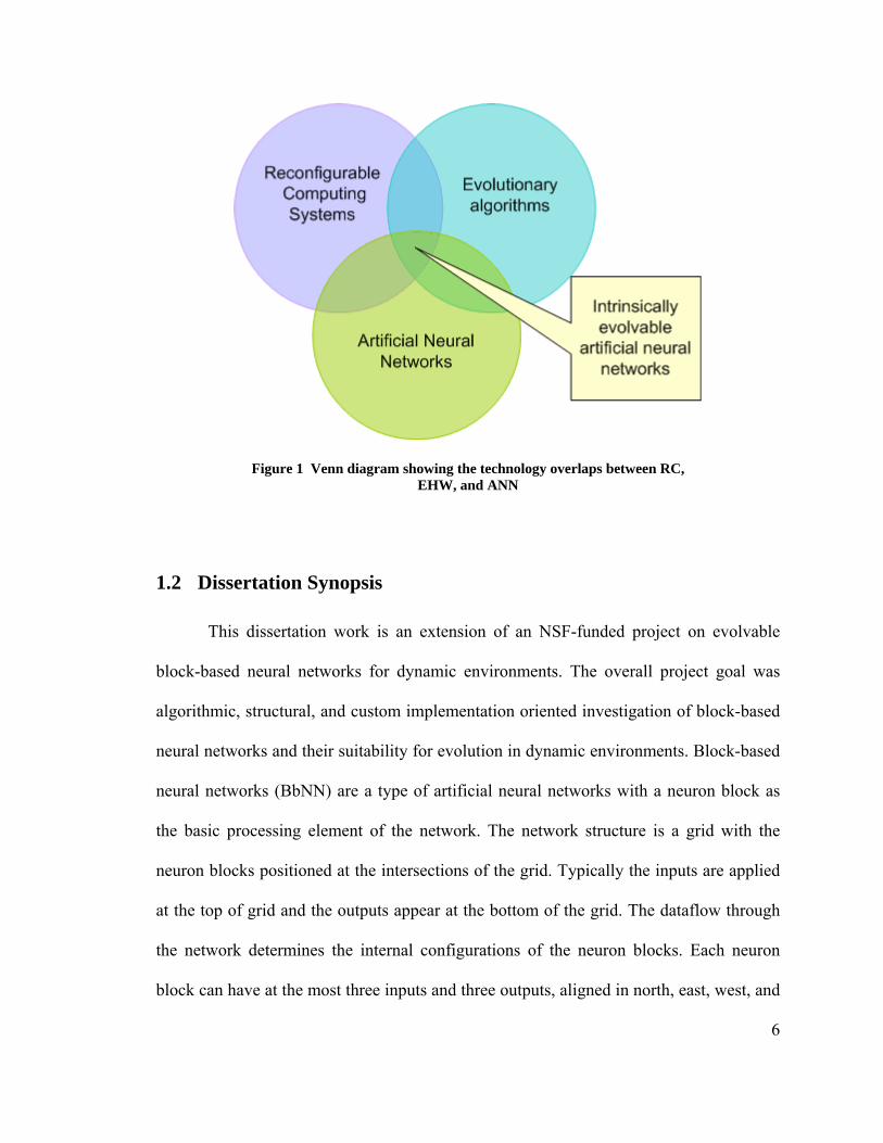
Figure 1 Venn diagram showing the technology overlaps between RC, EHW, and ANN
1.2 Dissertation Synopsis
This dissertation work is an extension of an NSF-funded project on evolvable
block-based neural networks for dynamic environments. The overall project goal was
algorithmic, structural, and custom implementation oriented investigation of block-based
neural networks and their suitability for evolution in dynamic environments. Block-based
neural networks (BbNN) are a type of artificial neural networks with a neuron block as
the basic processing element of the network. The network structure is a grid with the
neuron blocks positioned at the intersections of the grid. Typically the inputs are applied
at the top of grid and the outputs appear at the bottom of the grid. The dataflow through
the network determines the internal configurations of the neuron blocks. Each neuron
block can have at the most three inputs and three outputs, aligned in north, east, west, and
6
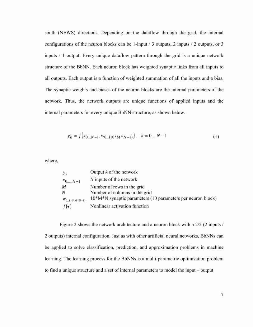
south (NEWS) directions. Depending on the dataflow through the grid, the internal
configurations of the neuron blocks can be 1-input / 3 outputs, 2 inputs / 2 outputs, or 3
inputs / 1 output. Every unique dataflow pattern through the grid is a unique network
structure of the BbNN. Each neuron block has weighted synaptic links from all inputs to
all outputs. Each output is a function of weighted summation of all the inputs and a bias.
The synaptic weights and biases of the neuron blocks are the internal parameters of the
network. Thus, the network outputs are unique functions of applied inputs and the
internal parameters for every unique BbNN structure, as shown below.
( )( ) 1....0,, 1**10...01...0 −== −− Nkwxfy NMNk (1)
where,
ky Output k of the network
1.....0 −Nx N inputs of the network M Number of rows in the grid N Number of columns in the grid
( 1**10...0 −NMw ) 10*M*N synaptic parameters (10 parameters per neuron block)
( )•f Nonlinear activation function
Figure 2 shows the network architecture and a neuron block with a 2/2 (2 inputs /
2 outputs) internal configuration. Just as with other artificial neural networks, BbNNs can
be applied to solve classification, prediction, and approximation problems in machine
learning. The learning process for the BbNNs is a multi-parametric optimization problem
to find a unique structure and a set of internal parameters to model the input – output
7
Figure 2 (a) Block-based neural network topology (b) 2 input / 2 output neuron block configuration
relationships in the training datasets. Thus, global search techniques such as genetic
algorithms (GAs) are used to train the BbNNs. Although GA training may take more time
to converge to a solution than gradient descent search techniques such as
backpropagation algorithm, it avoids getting trapped in the local minima, a problem often
faced with backpropagation training algorithm. Hybrid training algorithms for BbNNs
have been investigated that take the advantages of global sampling of GAs and fast
convergence of gradient descent techniques for efficient training of BbNNs. More
information on these can be found in [4-6]. The research work presented in this
dissertation uses genetic algorithms to train the BbNNs.
8
This dissertation presents an intrinsically evolvable implementation of BbNNs on
RC systems. The implementation supports functional-level intrinsic evolution with
neuron blocks as the functional modules for the EHW system. The dissertation also
9
presents online learning techniques with BbNNs and performance characterization of
these networks on RC systems. The major contributions from this research work are as
follows:
1. RC implementation of an intrinsically evolvable platform for BbNNs. The
platform supports on-chip evolution (evolutionary algorithm + BbNN on the same
FPGA) of BbNNs.
2. Online training algorithm to evolve BbNNs on-chip, in field enabling applications
in dynamically variant environments.
3. Performance characterization of BbNNs on RC systems. The performance model
presented enables quantitative and qualitative performance comparison across
different computing platforms such as general purpose computing and RC
systems.
1.3 Manuscript Organization
Chapter 2 introduces artificial neural networks and provides a review of reported
literary contributions to neural hardware implementations. Chapter 3 introduces
evolvable hardware systems and provides a review of reported literary contributions to
applications of EHW systems. Chapter 4 introduces block-based neural networks and
discusses multi-parametric genetic evolution of these networks. Chapter 5 gives the
design details of the intrinsically evolvable BbNN implementation on RC systems and
demonstrates the on-chip training ability of the BbNN platform. Chapter 6 provides
10
details on the online evolution algorithm for BbNNs. It demonstrates the advantages of
online evolution using a case study, ‘Adaptive Neural Luminosity Controller’. Chapter 7
introduces a performance characterization model for BbNNs on RC systems. The model
enables quantitative and qualitative performance comparison across different computing
platforms. Chapter 8 concludes the dissertation providing a summary of the research
work accomplished and the prospects of future research directions in the field.
2 ARTIFICIAL NEURAL NETWORKS
2.1 Introduction to Artificial Neural Networks
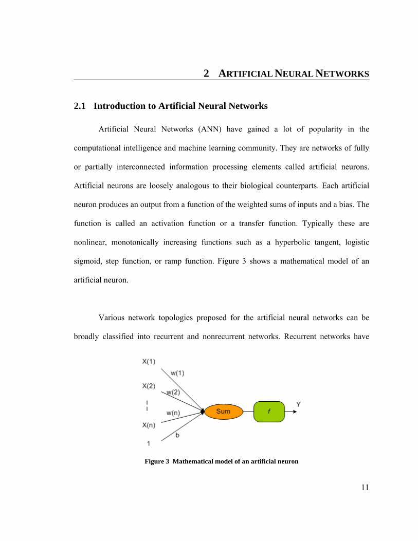
Artificial Neural Networks (ANN) have gained a lot of popularity in the
computational intelligence and machine learning community. They are networks of fully
or partially interconnected information processing elements called artificial neurons.
Artificial neurons are loosely analogous to their biological counterparts. Each artificial
neuron produces an output from a function of the weighted sums of inputs and a bias. The
function is called an activation function or a transfer function. Typically these are
nonlinear, monotonically increasing functions such as a hyperbolic tangent, logistic
sigmoid, step function, or ramp function. Figure 3 shows a mathematical model of an
artificial neuron.
Various network topologies proposed for the artificial neural networks can be
broadly classified into recurrent and nonrecurrent networks. Recurrent networks have
Figure 3 Mathematical model of an artificial neuron
11
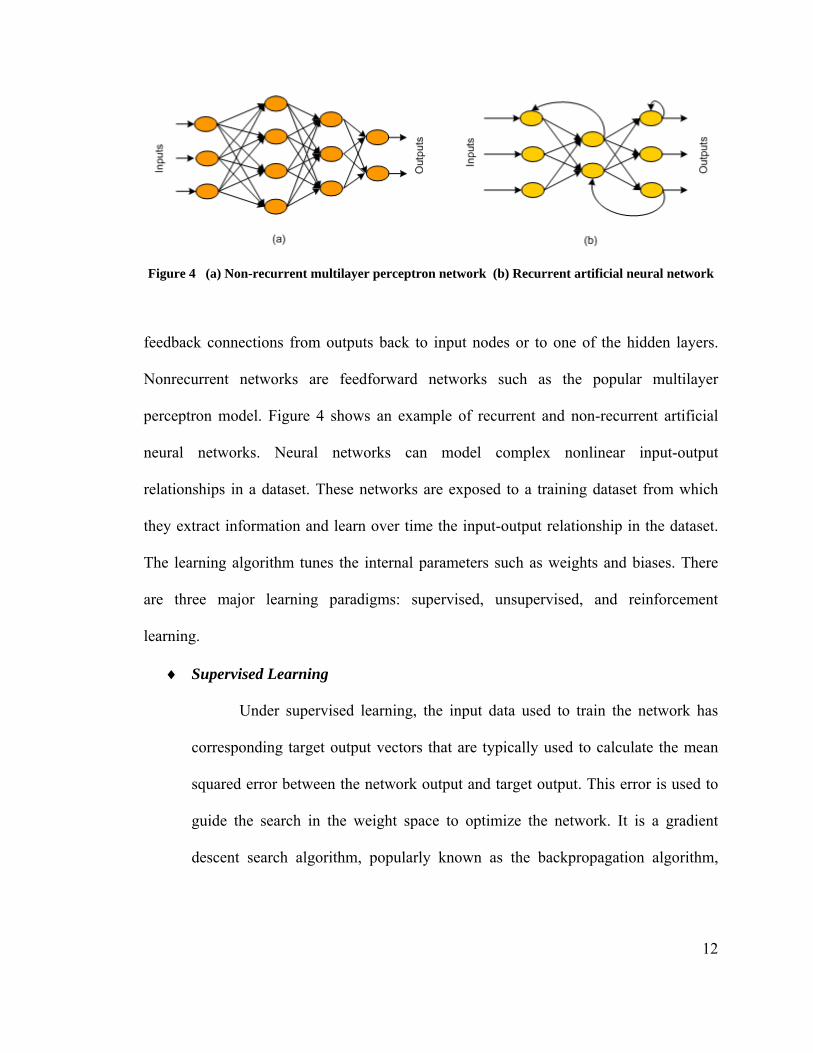
Figure 4 (a) Non-recurrent multilayer perceptron network (b) Recurrent artificial neural network
12
feedback connections from outputs back to input nodes or to one of the hidden layers.
Nonrecurrent networks are feedforward networks such as the popular multilayer
perceptron model. Figure 4 shows an example of recurrent and non-recurrent artificial
neural networks. Neural networks can model complex nonlinear input-output
relationships in a dataset. These networks are exposed to a training dataset from which
they extract information and learn over time the input-output relationship in the dataset.
The learning algorithm tunes the internal parameters such as weights and biases. There
are three major learning paradigms: supervised, unsupervised, and reinforcement
learning.
♦ Supervised Learning
Under supervised learning, the input data used to train the network has
corresponding target output vectors that are typically used to calculate the mean
squared error between the network output and target output. This error is used to
guide the search in the weight space to optimize the network. It is a gradient
descent search algorithm, popularly known as the backpropagation algorithm,
13
which tries to minimize the total mean squared error between network and target
output [3].
♦ Unsupervised Learning
Unsupervised learning uses no external teacher and is based upon only
local information. It is also referred to as self-organization, in the sense that it
self-organizes data presented to the network and detects their emergent collective
properties. Hebbian learning and the competitive learning are the two types of
widely used unsupervised learning techniques [3].
♦ Reinforcement Learning
In reinforcement learning an agent learns from interaction with the
environment. At every time step, the agent performs an action and the
environment generates an observation and an instantaneous cost depending on the
agent’s action. The environment is modeled as a Markov decision process (MDP)
with sets of states and actions, and the probability distributions for costs,
observations, and state-action transitions. The policy of selecting the actions is
defined as a conditional distribution over actions given the observations. The aim
is to discover a policy for selecting actions that minimizes some measure of a
long-term cost, i.e. the expected cumulative cost [7].
Artificial neural networks are widely used in pattern classification, sequence
recognition, function approximation, and prediction. Many successful artificial neural
network implementations have been reported with applications in medical diagnostics,
autonomously flying aircrafts, and credit card fraud detection systems.

14
2.2 Historical Perspective
Fascination with building machines that can demonstrate some degree of human-
like intelligent behavior has driven the research efforts in the fields of artificial
intelligence. Alan Turing in his classic 1950 paper in Mind, “Computing Machinery and
Intelligence” laid out the test for machine intelligence, what is now famously known as
the Turing test for the quality of artificial intelligence [8]. He proposed that if a machine
can intelligently converse with a human such that an external observer cannot distinguish
between the two, the machine is intelligent. The pursuit of intelligent machines and
fascination with the human brain lead to the evolution of the fields of artificial
intelligence and machine learning. In a 1943 classic paper McCulloch and Pitts described
the logical calculus of neural networks, proposing that a neuron follows an all-or-none
law [9]. If a sufficient number of these neurons with their synaptic connections set
properly operate synchronously, then in principle it could compute any computable
function. Donald Hebb, in his 1949 book The Organization of Behavior, used the
McCulloch-Pitts model of neurons and presented a physiological learning rule for
synaptic modifications [10]. Hebb’s learning rule suggested that the effectiveness of a
variable synapse between two neurons is increased by the repeated activation of one
neuron by the other across the synapse. He proposed that the connectivity of the brain is
continuously changing as an organism learns differing functional tasks, and that neural
assemblies are created by such changes. This view of the brain dynamically evolving its
internal synaptic connections has been widely accepted and many later neural models for
machine learning have adopted this functional philosophy to a varying degree. Some 15
years after the publication of McCulloch and Pitts’s classic paper on the logical calculus
15
of neural network models, Rosenblatt in 1958, introduced a new neural learning
technique for pattern recognition problem in his work on the perceptron [11]. In 1960,
Widrow and Hoff proposed a different training algorithm than the perceptron
convergence theorem, the least mean-square (LMS) algorithm and used it to formulate
the Adaline (adaptive linear element) [12]. One of the earliest trainable layered neural
networks with multiple adaptive elements was the Madaline (multiple-adaline) proposed
by Widrow and his students in 1962 [13]. After an initial upsurge in the research into
perceptron based neural networks came the downside after a 1969 book by Minsky and
Papert, titled ‘The Perceptron’ in which they mathematically demonstrated fundamental
limitations on what single-layer perceptrons could compute [14]. This was followed by a
decade of dormancy in the field of artificial neural networks until Hopfield’s classic
paper in 1982 brought together many older ideas that helped revive the field of artificial
neural networks [15]. Since then they have gained a lot of popularity in the computational
intelligence and machine learning community.
2.3 Building Artificial Neural Networks
To build realizable intelligent systems with artificial neural networks we need to
design networks with flexible synaptic connections capable of evolving dynamically as
the network learns new behavior. A lot of earlier work on artificial neural networks was
based on software simulations of neural network training to obtain an optimized network
which was then implemented in hardware for faster recall speeds. The trial and error
based training algorithms for these networks make application specific integrated circuit
16
(ASIC) implementations of on-chip training challenging. The dynamic structure and
parameter updates required during training are harder to implement on an ASIC.
Consider the hugely popular multilayer Perceptron (MLP) model of an ANN. The MLP is
a feedforward neural network comprised of layers of artificial neurons typically trained
using the backpropagation algorithm. The first layer is called the input layer, the last
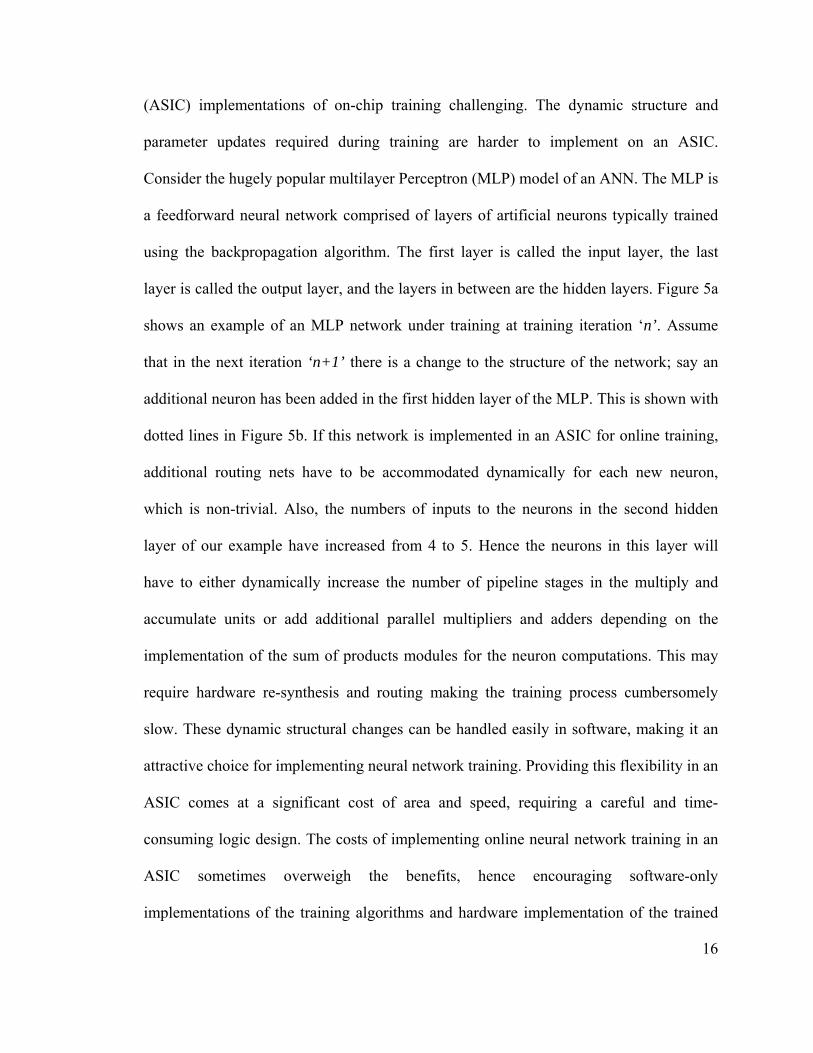
layer is called the output layer, and the layers in between are the hidden layers. Figure 5a
shows an example of an MLP network under training at training iteration ‘n’. Assume
that in the next iteration ‘n+1’ there is a change to the structure of the network; say an
additional neuron has been added in the first hidden layer of the MLP. This is shown with
dotted lines in Figure 5b. If this network is implemented in an ASIC for online training,
additional routing nets have to be accommodated dynamically for each new neuron,
which is non-trivial. Also, the numbers of inputs to the neurons in the second hidden
layer of our example have increased from 4 to 5. Hence the neurons in this layer will
have to either dynamically increase the number of pipeline stages in the multiply and
accumulate units or add additional parallel multipliers and adders depending on the
implementation of the sum of products modules for the neuron computations. This may
require hardware re-synthesis and routing making the training process cumbersomely
slow. These dynamic structural changes can be handled easily in software, making it an
attractive choice for implementing neural network training. Providing this flexibility in an
ASIC comes at a significant cost of area and speed, requiring a careful and time-
consuming logic design. The costs of implementing online neural network training in an
ASIC sometimes overweigh the benefits, hence encouraging software-only
implementations of the training algorithms and hardware implementation of the trained
network to achieve higher connections per second (CPS) recall speeds. Section 2.5
provides a review of the neural hardware implementations reported in the literature.
Figure 5 Multilayer Perception Example (a) Training Iteration ‘n’ (b) Training iteration ‘n+1’
2.4 Genetic Evolution of Artificial Neural Networks
The popularly used backpropagation algorithm for the training of ANNs, being a
gradient descent approach, has two drawbacks as outlined by Sutton [16]. First, the
search often gets trapped in local minima if the gradient step is too small, whereas for
large gradient steps it could have an oscillatory behavior. The method is inefficient in
searching for global minima, especially with multimodal and nondifferentiable search
spaces. Second, there is a problem of catastrophic interference with these methods. There
is a high level of interference between learning with different patterns, because those
units that have so far been found most useful are also the ones most likely to be changed
to handle new patterns. The problem of global minima can be solved by using global
search procedures like genetic algorithms. Many researchers have proposed using genetic
algorithms to evolve neural networks to find optimized candidates in the large deceptive
17
18
multimodal search spaces [17-25]. Genetic algorithms (GAs) evolve a population of
neural networks, encoded as chromosomes over multiple generations using genetic
operators such as selection, crossover, and mutation. A population of chromosomes is
first ranked according to their fitness levels. The fitness is usually determined from the
mean squared error between the target and the actual outputs of each individual network
in the population. A selection scheme selects the chromosomes from the population based
on their rankings for reproduction via genetic crossover and mutation. The survival of the
fittest policy tends to increase the average fitness of the population over multiple
generations. The evolution continues over multiple generations until either a chromosome
with fitness at least equal to the predetermined target fitness is found or the preset
maximum number of generations is reached.
GA, being a global search algorithm, avoids the pit-falls of local minima faced in
gradient descent algorithms. It does not need to calculate derivatives of the error function
and hence works very well with nondifferentiable error surfaces. Also there are no
restrictions on network topologies as long as an appropriate fitness function can be
defined for the network, network structure, and internal parameters encoded as
chromosomes. Thus GA can handle a wide variety of artificial neural networks, but the
evolutionary approach is a computationally intensive approach. It is also slower than the
directed gradient descent based training algorithms such as the backpropagation
algorithm [16]. Genetic evolution, being an adaptive process, is good at global sampling,
but performs poorly for local fine tuning. If the initial guess of the network is closer in
proximity on the error surface to the global minimum, the gradient descent based search
19
algorithm may converge much faster than a global sampling technique such as the genetic
algorithms. If the neural network is more complex with multiple hidden neural layers, the
error surface will be complex, with many discontinuities. In such cases, gradient descent
search algorithms often will be stuck in local minima and will not converge to the global
minimum, whereas, the global search techniques such as GAs are more likely to find the
optimal answer.
In this work we concentrate mainly on a type of neural networks called block-
based neural networks (BbNN) [23] and use GA to train the network structure and the
internal parameters of the BbNNs. Chapter 4 introduces BbNNs.
2.5 Review of Neural Hardware Implementations
This section provides a brief overview of reported work in the literature for
artificial neural network hardware implementations.
2.5.1 Neural Network Hardware
Dedicated hardware units for neural networks are called neurochips or
neurocomputers [26]. Due to limited commercial prospects and their required
development and support resources, these chips have seen little commercial viability.
Also, due to the existence of wide-ranging neural network architectures and a lack of a
complete and comprehensive theoretical understanding of their capabilities, most
commercial neurocomputer designs are dedicated implementations of popular paradigms
such as multilayer perceptrons, Hopfield networks, or Kohonen networks. Various
20
classification and overview studies of neural hardware have appeared in the literature
[26-36]. Heemskerk has a detailed review of neural hardware implementations until about
1995 [26]. He classified the neural hardware according to their implementation
technologies such as the neurocomputers built using general purpose processors, digital
signal processors, or custom implementations using analog, digital, or mixed-signal
design. Zhu et al has a good survey of ANN FPGA implementations up until 2003 [36].
The neural network hardware review presented in this dissertation addresses custom
hardware implementations of artificial neural networks. These are more directly related to
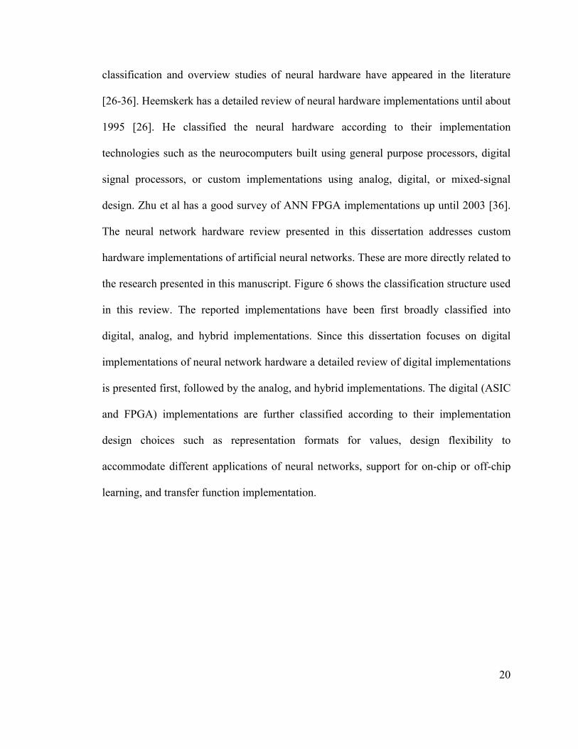
the research presented in this manuscript. Figure 6 shows the classification structure used
in this review. The reported implementations have been first broadly classified into
digital, analog, and hybrid implementations. Since this dissertation focuses on digital
implementations of neural network hardware a detailed review of digital implementations
is presented first, followed by the analog, and hybrid implementations. The digital (ASIC
and FPGA) implementations are further classified according to their implementation
design choices such as representation formats for values, design flexibility to
accommodate different applications of neural networks, support for on-chip or off-chip
learning, and transfer function implementation.
Figure 6 Neural network hardware classification
2.5.2 Digital Neural Network Implementations
Digital neural network implementations offer high computational precision,
reliability, and programmability. The implementations are targeted towards either ASICs
or FPGAs. The synaptic weights and biases of the neurons in the network can be stored
on or off chip, representing a trade-off between the speed and the size of the design.
ASIC neurochips can achieve higher processing speeds, lower power, and more density
than corresponding FPGAs implementations, but have significantly higher design and
fabrication costs. FPGAs have slower processing speeds than ASICs but have the
advantage of runtime circuit reconfigurations allowing reuse of the FPGA chip for
21
22
different applications. FPGAs are commercial-off-the-shelf products, lowering the
implementation costs significantly. The last decade has seen a lot of advancement in
reconfigurable hardware technology. FPGA chips with built-in RAMs, multipliers,
gigabit transceivers, on-chip embedded processors, and faster clock speeds have attracted
many neural network FPGA implementations. In general, the digital implementation
disadvantages as compared to the analog implementations are relatively larger circuit
sizes and higher power consumption, but digital implementations our easier to build and
scale as compared to their analog counterparts.
2.5.2.1 Real Value Representation
Digital neural network hardware implementations represent the real valued
weights, biases, and I/O using fixed point, floating point, or specialized representations
such as pulse stream encoding. The choice of a particular representation is a trade-off
between arithmetic circuit size and speed, data precision, and the available dynamic range
for the real values. Floating point arithmetic units are slower, larger, and more
complicated than their fixed point counterparts, which are faster, smaller, and less
complicated.
Generally, floating point representations of real valued data for neural networks
are found in custom ASIC implementations. Aibe et al. [37] used floating point
representation for their implementation of probabilistic neural networks (PNNs). In
PNNs, the estimator of the probabilistic density functions is very sensitive to the
23
smoothing parameter (the network parameter to be adjusted during neural network
learning). Hence, a very high accuracy is needed for the smoothing parameter, making
floating point implementations more attractive. Ayela et al. demonstrated an ASIC
implementation of MLPs using a floating point representation for weights and biases
[38]. They also support on-chip neural network training using the backpropagation
algorithm and are listed also in section 2.5.2.3. Ramacher et al. present a digital
neurochip called SYNAPSE-1 [39, 40]. It consists of a 2-dimensional systolic array of
neural signal processors that directly implement parts of common neuron processing
functions such as matrix-vector multiplication and finding maximum. These processors
can be programmed for specific neural networks. All the real values are represented using
floating point representation.
For FPGA implementations the preferred choice is fixed point representation.
Despite the current advances in technology, the floating-point representation of real
valued data may still be impractical to implement in FPGAs. Larger arithmetic circuit
sizes limit the neural network sizes that can be implemented on a single FPGA [41].
Moussa, Arebi, and Nichols demonstrate an implementation of MLP on FPGAs using
fixed and floating point representations. Their results show that the MLP implementation
using fixed point representation was over 12x greater in speed, over 13x smaller in area,
and achieves far greater processing density as compared to the MLP using floating point
representations [42]. There exists a body of research to show that it is possible to train
ANNs with fixed point weights and biases [42-44]. But there is a delicate trade-off
between minimum precision, dynamic data range, and the area required for the
24
implementation of arithmetic units. A finer precision will have fewer quantization errors
but requires larger multiply-accumulate units, whereas smaller bit width, lower precision
arithmetic unit implementations are smaller, faster, and more power efficient. But due to
lesser precision there are larger quantization errors that could severely limit the ANN’s
capabilities to learn and solve a problem. There is a tradeoff between precision and
area/speed, and a way to resolve this conflict is to select a ‘minimum precision’ that
would be required for a target application. Holt and Baker, Holt and Hwang, and Holi and
Hwang investigated the minimum precision problem on a few ANN benchmark
classification problems using simulations and found 16-bit data widths with 8-bit
fractional parts were sufficient for networks to learn and correctly classify the input
datasets [43-45]. Ros et al. demonstrate a successful fixed point implementation of
spiking neural networks on FPGAs [46]. Pormann et al. demonstrate fixed point
implementations of neural associative memories, self-organizing feature maps, and basis
function networks on FPGAs [47]. Some other reported implementations that used fixed
point representations can be found in [48-56].
The trade-offs between fixed and floating point representations are due to area
and speed of the arithmetic circuits (especially the multipliers and accumulators) required
in the implementation of the neural computations. Researchers have proposed different
encoding techniques that simplify the designs of the arithmetic circuits. Marchesi et al.
proposed special training algorithms for multilayer perceptrons that use weight values
that are powers of two. The weight constraint eliminates any need for multipliers in the
ANN implementations as they are replaced with simple shifters [57]. Other approaches
25
encode real values in bit streams and implement the multipliers in bit-serial fashion,
serializing the flow and using simple logic gates instead of complex, expensive
multipliers for smaller and faster arithmetic units. But the disadvantage of using a pulse
stream arithmetic approach is the precision limitation which can severely affect ANNs
capability to learn and solve a problem. Also, for multiplications to be correct, the bit
streams should be uncorrelated. To produce these would require independent random
sources which again require larger resources to implement. Murray and Smith’s VLSI
implementation of ANNs [58], used pulse-stream encoding for real values which was
later adopted by Lysaght et al. [59] for ANN implementations on Atmel FPGAs.
Implementation using pulse stream encoding can also be found in [60, 61]. The
advantage of using serial stochastic bit streams for encoding real valued data is that the
product of the two stochastic bit streams can be computed using a simple bitwise ‘xor’.
Implementations using these can be found in [62-65]. Economou et al. show a pipelined
bit serial arithmetic implementation for ANNs [66]. Salapura used delta encoded binary
sequences to represent real values and used bit stream arithmetic to calculate a large
number of required parallel synaptic calculations [67]. Zhu and Sutton [34] has a good
survey of hardware implementations of artificial neural networks using pulse stream
arithmetic.
Researchers have also proposed other approaches as discussed next. Chujo et al.
have proposed an iterative calculation algorithm of the perceptron type neuron model,
which is based on multidimensional binary search algorithm. Since binary search doesn’t
need any sum of products functionality, it eliminates the need for expensive multiplier

26
circuitry in hardware [68]. Guccione and Gonzalez used a vector-based data parallel
approach to represent real values and compute the sum of products [69]. The distributed
arithmetic (DA) approach of Mintzer for implementing FIR filters on FPGAs [70] was
used by Szabo et al. for a digital implementation of pre-trained neural networks. They
used Canonic Signed Digit Encoding (CSD) to improve the hardware efficiency of the
multipliers [71]. Noory and Groza also used the DA neural network approach and
targeted their design for implementation on FPGAs [72]. Pasero and Perri use LUTs to
store all the possible multiplication values in an SRAM to avoid implementing costly
multiplier units in FPGA hardware. At system boot-up a microcontroller computes all the
possible product values of the fixed weight and an 8-bit input vector, and loads it into the
SRAM [73].
The neural network hardware implementation presented in this dissertation is on
FPGAs. As discussed above floating point implementations of neural networks on
FPGAs may not be practical. Larger floating point arithmetic circuits limit the size of the
neural networks that can be implemented on the FPGA [41]. Also, there exists a body of
research to show that it is possible to train ANNs with fixed point weights and biases [42-
44]. Hence, the chosen approach chosen for representing real valued data in the neural
network FPGA implementation presented in this dissertation is fixed point.
27
2.5.2.2 Design Flexibility
An important design choice for neural network hardware implementations is the
degree of structure adaptation and synaptic parameter flexibility. An implementation of a
neural network with fixed network structure and weights can only be used in the recall
stage and cannot be adapted to different network structures and parameters without a
hardware redesign. One motivation of using FPGAs for ANN implementations is the
advantage of circuit adaptation using runtime reconfigurations. Runtime reconfigurations
can be used to load different neural network circuit designs for different applications,
reducing the implementation cost substantially by reusing the FPGA. Hardware redesigns
in an ASIC are much more expensive and time consuming due to fabrication costs and
time. FPGAs are used in neural network implementations for different purposes such as
prototyping and simulation, density enhancement, and topology adaptation. The purpose
of using FPGAs for prototyping and simulation is to thoroughly test a prototype of the
final design for correctness and functionality before sending it for expensive ASIC
fabrication. This approach was used in [74]. Full or partial FPGA reconfigurations can
be used to implement larger circuits, which a single FPGA cannot hold, via temporal
folding. This increases the amount of effective functionality per unit reconfigurable
circuit area of FPGAs. Eldredge et al. used this technique to implement the
backpropagation training algorithm on the FPGAs. The algorithm was divided temporally
in three different executable stages and each stage was loaded on the FPGA using
runtime reconfigurations. More details on this and other follow up implementations to
Eldredge’s technique are covered in section 2.5.2.3 for on-chip learning [75, 76]. The
runtime reconfiguration in FPGAs can also be used for topology adaptation. Neural
networks with different structure and internal parameters targeting different applications
can be loaded on the FPGA via runtime reconfigurations. One of the earliest
implementations of artificial neural networks on FPGAs, the Ganglion connectionist
classifier, used FPGA reconfigurations to load networks with different structures for each
new application of the classifier [77]. This approach to use full or partial FPGA runtime
reconfigurations for structure and/or parameter adaptation can also be seen in the neural
network implementations of Perez-Uribe et al. [78-80], Restrepo et al. [81], Ros et al.
[46], Kothandaraman [49], Ferrer et al. [50], Chin Tsu, Wan-de, and Yen-Tsun [51],
Wang et al. [52], Syiam et al. [53], Krips, Lammert, and Kummert [54], Zhu, Milne, and
Gunther [55], and Kurokawa and Yamashita [82].
The approach of using FPGA runtime reconfigurations for topological adaptation
is acceptable when the neural network is trained offline using software simulations. For
online trainable implementations of neural networks the overheads of FPGA
reconfigurations far outweigh any benefits. Typical current generation FPGA
reconfiguration times are of the order of a few milliseconds (see Table 1). Overall
performance of the system using reconfigurations for topological adaptation during
online training depends on the total amount of time spent performing computations
versus the time spent in reconfiguration cycles. Guccione and Gonazalez investigated this
issue and came up with the following equation reported in [83]:
)1/( −= srq (2)
28
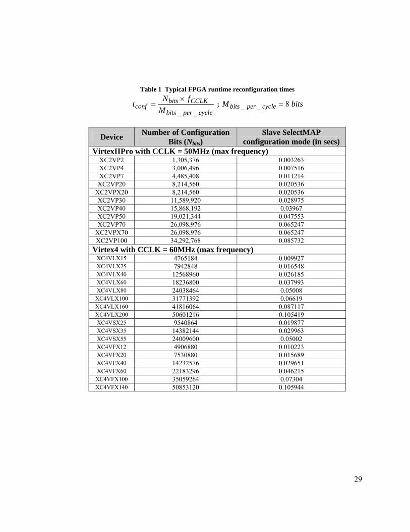
Table 1 Typical FPGA runtime reconfiguration times
cycleperbits
CCLKbitsconf M
fNt
__
×= ; bitsM cycleperbits 8__ =
Device Number of Configuration Bits (Nbits)
Slave SelectMAP configuration mode (in secs)
VirtexIIPro with CCLK = 50MHz (max frequency) XC2VP2 1,305,376 0.003263 XC2VP4 3,006,496 0.007516 XC2VP7 4,485,408 0.011214
XC2VP20 8,214,560 0.020536 XC2VPX20 8,214,560 0.020536 XC2VP30 11,589,920 0.028975 XC2VP40 15,868,192 0.03967 XC2VP50 19,021,344 0.047553 XC2VP70 26,098,976 0.065247
XC2VPX70 26,098,976 0.065247 XC2VP100 34,292,768 0.085732
Virtex4 with CCLK = 60MHz (max frequency) XC4VLX15 4765184 0.009927 XC4VLX25 7942848 0.016548 XC4VLX40 12568960 0.026185 XC4VLX60 18236800 0.037993 XC4VLX80 24038464 0.05008 XC4VLX100 31771392 0.06619 XC4VLX160 41816064 0.087117 XC4VLX200 50601216 0.105419 XC4VSX25 9540864 0.019877 XC4VSX35 14382144 0.029963 XC4VSX55 24009600 0.05002 XC4VFX12 4906880 0.010223 XC4VFX20 7530880 0.015689 XC4VFX40 14232576 0.029651 XC4VFX60 22183296 0.046215
XC4VFX100 35059264 0.07304 XC4VFX140 50853120 0.105944
29
30
where s denotes the computational time, r denotes the reconfiguration time, and q is the
number of times the configured logic should be used before another configuration is tried
to achieve good performance. Thus, time spent in FPGA computations must be much
higher than the time spent in FPGA reconfiguration cycles to achieve reasonable
performance speedups.
The neural network implementation presented in this dissertation is an online
trainable neural network implementation on FPGAs. It supports dynamic structure and
parameter updates to the neural network without FPGA reconfigurations. The
implemented network topology and design details are in chapters 4 and 5, respectively.
ASIC implementations of flexible neural networks that can adapt structure and
parameter values have been reported in literature. One commercially available dedicated
neural hardware design is the Neural Network Processor (NNP) from Accurate
Automation Corp. [84]. It is a neural network processor that has instructions for various
neuron functions such as multiply and accumulate or transfer function calculation. Thus
the neural network can be programmed using the NNP assembly instructions for different
neural network implementations. Mathia and Clark compared performance of a single
and parallel (1 to 4 NNPs) multiprocessor NNP against that of the Intel Paragon
Supercomputer (1 to 128 parallel processor nodes). The NNP outperformed the Intel
Paragon by a factor of 4 [85].
31
2.5.2.3 On-chip/Off-chip Learning
Neural network training algorithms are typically iterative algorithms that adjust
neural network parameters and structure over multiple iterations based on a cost function.
Thus to do an on-chip training, one needs a design that can be dynamically adapted to
change its network structure and parameters. Few implementations reported in the
literature actually support an on-chip training of neural networks due to the complexities
involved. Eldredge et al. reported an implementation of the backpropagation algorithm on
FPGAs by temporally dividing the algorithm into three sequentially executable stages of
the feedforward, error backpropagation, and synaptic weight update [75, 76]. The feed-
forward stage feeds in the inputs to the network and propagates the internal neuronal
outputs to output nodes. The backpropagation stage calculates the mean squared output
errors and propagates them backward in the network in order to find synaptic weight
errors for neurons in the hidden layers. The update stage adjusts the synaptic weights and
biases for the neurons using the activation and error values found in the previous stages.
Hadley et al. improved the approach of Eldredge by using partial reconfiguration of
FPGAs instead of full-chip runtime reconfiguration [86]. Gadea et al. show a pipelined
implementation of the backpropagation algorithm in which the forward and backward
passes of the algorithm can be processed in parallel on different training patterns, thus
increasing the throughput [87]. Ayala et al. demonstrated an ASIC implementation of
MLP with on-chip backpropagation training using floating point representation for real
values and corresponding dedicated floating point hardware [38]. The backpropagation
algorithm implemented is similar to that of Eldredge et al. [75, 76]. A ring of 8 floating
point processing units (PU) are used to compute the intermediate weighted sums in the
32
forward stage and the weight correction values in the weight update stage. The size of the
memories in the PUs limits the number of neurons that can be simulated per layer to 200.
A more recent FPGA implementation of backpropagation algorithm can be found in [88].
Witkowski, Neumann, and Ruckert demonstrate an implementation of hyper basis
function networks for function approximation [89]. Both learning and recall stages of the
network are implemented in hardware to achieve higher performance. The GRD (Genetic
Reconfiguration of DSPs) chip by Murakawa et al. can perform on-chip online evolution
of neural networks using genetic algorithms [90]. Details on it are covered in chapter 3 on
evolvable hardware systems. Two commercially available neurochips from the early
1990s are the CNAPS (Hammerstrom [91]) and MY-NEUPOWER (Sato et al. [92]).
CNAPS was a SIMD array of 64 processing elements per chip that are comparable to low
precision DSPs and was marketed commercially by Adaptive solutions. The complete
CNAPS system consisted of a CNAPS server which connected to a host workstation, and
Codenet, a set of software development tools. It supports Kohonen LVQ (linear vector
quantization), backpropagation, and convolution at high speed. Another commercially
available on-chip trainable neurocomputer is MY-NEUPOWER. It supports various
learning algorithms such as backpropagation, Hopfield, and LVQ and contains 512
physical neurons. It was a neural computational engine for software packet called
NEUROLIVE [92].
The following references discuss analog and hybrid implementations that support
on-chip training. Zheng et al. have demonstrated a digital implementation of
backpropagation learning algorithm along with an analog transconductance-model neural
33
network [93]. A digitally-controlled synapse circuit and an adaptation rule circuit with a
R-2R ladder network, a simple control logic circuit, and an UP/DOWN counter are
implemented to realize a modified technique for the backpropagation algorithm. Linares-
Barranco et al. also show an on-chip trainable implementation of an analog
transconductance-model neural network [94]. Field Programmable Neural Arrays
(FPNA), an analog neural equivalent of FPGAs, are a mesh of analog neural models
interconnected via a configurable interconnect network [95-99]. Thus, different neural
networks structures can be created dynamically, enabling on-chip training.
A more typical implementation approach has been to train the network offline
using software simulations and implement the network obtained in hardware for faster
recall speeds. [46, 48-50, 52, 53, 100, 101] adhere to this approach.
Newer FPGA generations have on-chip embedded processors that some
implementations have used to run the training algorithms and thus provide in-system
network training. Schmitz et al. use the embedded processor on the FPGA to implement
genetic algorithm operators like selection, crossover, and mutation [102]. This FPGA is
closely coupled as a coprocessor to a reconfigurable analog artificial neural network
ASIC on a single PCB. A host processor initializes this PCB and oversees the genetic
evolution process.
34
2.5.2.4 Activation Function Implementation
Activation functions, or transfer functions, are typically non-linear monotonically
increasing sigmoid functions. Examples of typical activation functions include hyperbolic
tangent, logistic sigmoid, and hard limit functions. Direct implementation of nonlinear
sigmoid functions in FPGAs can occupy significant reconfigurable resources. A typical
approach is to use piece-wise linear approximations of these functions and interpolate the
values between piece-wise samples using straight lines. The computations for piecewise
approximations can either be implemented in logic or the values can be pre-computed
and stored in lookup tables (LUTs). Omondi, Rajapakse, and Bajger show an
implementation of piece-wise linear approximation of activation functions using the
CORDIC algorithm on FPGAs [103]. Krips et al. show an implementation of piece-wise
linear approximation of activation functions pre-computed and stored in LUTs [54].
One problem of direct implementations of the activation function is that one has
to redesign the hardware logic for every application that is using a different activation
function. In such scenarios the LUT approach serves well as the values can be pre-
computed and loaded in the LUT. But the size of the LUT is directly influenced by the
data widths. Every extra bit in the data more than doubles the size of the LUT.
35
2.5.3 Analog Neural Hardware Implementations
Analog artificial neurons are more closely related to their biological counterparts
as the biological neurons perform analog computations. Many characteristics of analog
electronics can be helpful for neural network implementations. Typical analog neurons
use operational amplifiers to directly perform neuron-like computations, such as
integration and sigmoid transfer functions. These can be modeled using physical
processes such as summing of currents or charges. Also, the interface to the environment
may be easier as no analog-to-digital and digital-to-analog conversions are required.
Some of the earlier analog implementations used resistors for representing free network
parameters such as synaptic weights [104]. These implementations using fixed weights
are not adaptable and hence can only be used in the recall phase. Adaptable analog
synaptic weight techniques represent weights using variable conductance [94, 105, 106],
voltage levels between floating gate CMOS transistors [107-110], capacitive charges
[111, 112], or using charged coupled devices [113, 114]. Some implementations use
digital memories for more permanent weight storage [115]. There have been many
commercial and research implementations of analog neural networks. Some of the
prominent ones are the Intel ETANN (Electronically Trainable Analog Neural Network)
[107, 116-120] and the Mod2 Neurocomputer [121]. Although there are many advantages
of implementing analog neural networks as discussed above, the disadvantage is that the
analog chips are susceptible to noise and process parameter variations, and hence need a
very careful design.
36
2.5.4 Hybrid Neural Hardware Implementations
Hybrid implementations combine analog, digital, and other strategies such as
optical communication links with mixed mode designs in an attempt to get the best that
each can offer. Typically the hybrid implementations use analog neurons taking
advantage of their smaller size and lower power consumption, and use digital memories
for permanent weight storage [122, 123]. But the mixed-signal design of the analog
neurons with the digital memories on the same die introduces a lot of noise problems and
requires isolation of the sensitive analog parts from the noisy digital parts using guard
rings. Sackinger et al. demonstrate a high speed character recognition application on the
ANNA (Analog Neural Network Arithmetic and logic unit) chip [124]. This ANNA chip
can be used for a wide variety of neural network architectures but is optimized for locally
connected weight-sharing networks, and time-delay neural networks (TDNNs). Zatorre-
Navarro et al. demonstrate a mixed mode neuron architecture for sensor conditioning
[125]. It uses an adaptive processor that consists of a mixed four-quadrant multiplier and
a current conveyor that performs the nonlinearity. Synaptic weight storage uses digital
registers and neural network training is performed off-chip.
Due to the large number of interconnections, routing quickly becomes a
bottleneck in digital ASIC implementations. Higher fan-in and fan-out neurons require
more drive strength resulting in larger transistor widths and more intermediate signal
drive buffers. Some researchers have proposed hybrid designs using optical
communication channels. Maier et al. [126] have shown a hybrid digital-optical
implementation that performs neural computations electronically, but the communication
37
links between neural layers uses an optical interconnect system. This increases the speed
of neural processing by a factor of one magnitude higher than a purely digital approach.
But on the flip side they increase hardware cost and complexity for transferring signals
between the electronic and the optical systems. Craven et al. [127] proposed using
frequency multiplexed communication channels to overcome the communication
bottleneck in fully connected neural networks.
2.6 Summary
Custom neural network hardware implementations can best exploit the inherent
parallelism in computations observed in artificial neural networks. Many
implementations have relied on offline training of neural networks using software
simulations. The trained neural network is then implemented in hardware. Although these
implementations have good recall speedups, they are not directly comparable to the
implementation reported here which supports on-chip training of neural networks. On-
chip trainable neural hardware implementations have also been reported in literature.
Most of the reported ones are custom ASIC implementations such as the GRD chip by
Murakawa et al. [90], on-chip backpropagation implementation of Ayala et al. [38],
CNAPS by Hammerstrom [91], MY-NEUPOWER by Sato et al. [92], and FPNA by
Farquhar, Gordon and Hasler [95]. FPGA based implementations of on-chip training
algorithms have also been reported such as the backpropagation algorithm
implementations in [75, 76, 86-88]. An online trainable implementation of hyper basis
function networks has been reported in [89]. The implementation presented here differs
38
from the reported ones in one or more of the following; (i) the artificial neural network
implemented, the block-based neural networks (see chapter 4), (ii) the training approach
using the genetic algorithms, and (iii) the FPGA implementation platform. The
implementation supports on-chip training without reliance on FPGA reconfigurations,
unlike some of the approaches listed above. It uses genetic algorithms to train the
BbNNs. The genetic operators such as selection, crossover, and mutation are
implemented on the embedded processor PPC 405 on the FPGA die, similar to the
approach of Schmitz et al. [102]. But unlike their approach the neural network designed
is a digital implementation in the configurable logic portion of the same FPGA chip.
Schmitz et al. [102] use a separate neural analog chip for fitness evaluations for the GA
running on PPC 405 on the closely coupled FPGA on the same PCB board.
3 EVOLVABLE HARDWARE SYSTEMS
Evolvable hardware systems (often called E-hard or EHW systems) are systems
built using programmable/reconfigurable hardware devices such as programmable logic
devices (PLDs), field programmable gate arrays (FPGAs), field programmable transistor
arrays (FPTAs), or custom-built programmable chips. The central idea of these systems is
to use the runtime hardware reconfiguration ability of these devices along with
evolutionary algorithms to evolve a digital or analog circuit. The configuration bitstream
(viewed as a phenotype in an evolutionary algorithm) for these devices is encoded as a
chromosome (viewed as a genotype) and evolved using evolutionary algorithms over
multiple generations. Genetic operators such as selection, crossover, and mutation are
applied to a randomly generated population of these chromosomes to create newer
generations. Fitter genotypes survive through multiple generations and are used for
breeding newer generations. The aim is to increase the average fitness of the population
from one generation to the next with the goal of finding a genotype with fitness that is
equal to greater than the target fitness. The population fitness is determined by a fitness
function which is application-specific. Apart from evaluating the correctness of the
EHW’s output for the training data set, the fitness function can also consider other
constraints such as circuit size, speed, or power. EHW systems were first conceptualized
by DeGaris back in 1992. He classified these systems into two classes: extrinsic and
intrinsic EHW systems [2].
39
40
EXTRINSIC EHW systems perform an offline evolution using software
simulations. The evolutionary algorithm is wrapped around a software
model of the hardware and evolution is done using software simulations.
The fittest evolved circuit is then used and configured on the hardware.
INTRINSIC EHW systems include the hardware in the evolution loop. It is
an online evolution technique that directly evolves the underlying
hardware circuitry.
This chapter introduces EHW systems and reviews reported contributions to this
field over the last one and a half decades. Section 3.1 discusses gate-level and functional-
level evolution strategies and their corresponding advantages and disadvantages. Section
3.2 provides a literature review of EHW systems.
3.1 Gate-level, Transistor-level, and Functional-level Evolution
Evolving an FPGA bitstream in essence is evolving gate-level logic circuitry. Due
to a time consuming evolution process, evolving larger circuits using this strategy is
impractical. Longer chromosomal lengths for larger circuits need larger memories to
store the genotype generations during evolution and need significantly higher processing
speeds to speedup the time-consuming evolution process. Larger circuits also mean
significantly larger search spaces. Evolutionary algorithms are global search algorithms
and as a result may take much longer to converge to a solution over many generations.
41
This limits the practical circuit sizes that can be used in the evolution process. Also, for
intrinsic gate-level evolution, slow circuit reconfigurations times may pose a significant
bottleneck for some applications. Typical FPGA reconfiguration times are on the order of
a few milliseconds (see section 2.5.2.2). The number of runtime reconfigurations that are
required during the intrinsic evolution process could be significantly high and depends on
the population size and number of generations required to meet the fitness goals. Hence
the evolution process will incur significant reconfiguration cycle time overheads which
may not be practical for many applications.
Just as FPGAs are used for gate-level evolution in EHW systems, FPTAs enable
development of transistor-level EHW systems. Field programmable transistor arrays
enable circuit reconfigurability at transistor levels allowing synthesis of analog, digital,
and mixed-signal electronic circuits. These devices consist of cells of programmable
transistors, resistors, and capacitors interconnected via programmable switches. FPTAs
can be used to build analog circuits such as amplifiers, and filters as well as digital logic
circuits. More details on FPTAs can be found in [128].
Higuchi et al. [129, 130] proposed to use the concepts of evolvable hardware
systems to do functional-level hardware evolution as opposed to the traditional gate-level
evolution. They proposed to evolve internal parameters and connections of higher-level
functional modules such as adders, multipliers, dividers, and sine generators. A criticism
for this approach has been that the circuit is limited in functionality by the available
hardware modules and newer functional modules may be required for a different
42
application. But this approach also significantly reduces the genotype length, facilitating
more complex practical circuits for evolution. Since the EHW concept involves the
evolution of desirable hardware circuits by genetic learning, without giving any
specifications in advance, it provides a contrasting bottom-up approach to the
conventional top-down hardware design methodology. Thus, different functional modules
can be used for different applications.
So for neuromorphic circuit applications, artificial neuron models can be used as
functional modules. The evolutionary algorithm can then be used to evolve the synaptic
connections and free parameters of artificial neural networks. Prior work uses
evolutionary algorithms instead of more traditional gradient descent approaches for
training artificial neural networks [17-25]. This work follows in their footsteps to develop
an intrinsically evolvable neural network EHW system. The following section provides a
review of reported literature in evolvable hardware systems.
3.2 Review of Evolvable Hardware Systems
Typical FPGAs are not suitable for EHW as they cannot be programmed with
random bitstreams due to the risk of damaging the device. The idea of intrinsic evolution
really took off after the introduction of Xilinx 6200 series FPGAs [2]. These FPGAs were
EHW friendly; the devices included a SRAM-cell-based architecture in which all internal
connections were unidirectional. Thus, no random configuration bits in these cells could
damage the device as it is impossible to connect two outputs together. So an evolutionary
43
algorithm can be allowed to manipulate the configuration of a real chip without the need
for any legality constraint checking. Xilinx also made the architecture of these chips
public, generating more interest in the field of evolvable hardware systems. Earlier
research before the Xilinx 6200 series FPGAs was mostly concentrated on the extrinsic
evolution strategy. In 1998, Xilinx stopped production of the 6200 series FPGAs and
introduced their next generation Virtex series FPGAs [131]. With these devices Xilinx
reverted back to the classic FPGA device layout with CLBs and a multidirectional
routing structure. This made the device unsafe for random bitstream configurations as the
outputs could be shorted together in this architecture. Also the detailed architecture of
these devices was not publicly available, since Xilinx aimed at mass-production of these
devices. This also ensured that circuits couldn’t be reverse-engineered from the
bitstreams. Thus for intrinsic evolution, the evolutionary algorithms needed to include the
Xilinx place and route tools in their loop. However, other researchers have proposed
alternative strategies using JBits. JBits comprises Java classes that provide an application
programming interface (API) into the Xilinx FPGA bitstreams. JBits provides the
capability of designing and dynamically modifying circuits in Xilinx FPGAs.
Hollingworth, Smith, and Tyrrell demonstrated safe intrinsic evolution on Xilinx Virtex
devices using JBits [132].
This section provides a brief summary of reported publications in the evolvable
hardware field. Section 3.2.1 surveys various EHW chips grouping them by their target
applications. Section 3.2.2 surveys developed EHW platforms for research and custom
evolutionary algorithms. [2, 133-137] discuss various EHW fundamentals and also have
44
reviews of EHW systems. More formal classification and comparison with bio-inspired
systems can be found in [138].
3.2.1 EHW Chips and Applications
EHW systems use off-the-shelf hardware (such as FPGAs) as well as custom-built
EHW chips to implement digital, analog, or mixed-signal evolutionary circuits. These
chips enable one or more of the evolutionary techniques, gate-level, transistor-level, and
functional-level evolution, to be implemented. EHW systems have been successfully
applied in many application areas such as neural hardware, signal and image processing,
control applications, analog electronics, and navigation systems. The review presented
here groups the EHW implementations by their application fields. An interesting feature
of many EHW systems is a degree of inherent fault tolerance due to the evolutionary
design approach. In theory, previously developed hardware circuits can be re-evolved in
the event of a fault to effectively ‘bypass’ the faulty component or section of the chip. In
practice, the degree of fault tolerance achievable varies and is the subject of research.
EHW systems also have applications in extreme temperature electronics. Stoica et al.
demonstrated fault tolerant electronic circuit designs using adaptive intrinsic circuit
redesign/reconfiguration during operation in extreme environments [139]. Their approach
is demonstrated on a prototype chip that can recover functionality at 250˚C.
45
3.2.1.1 EHW Systems for Neural Hardware
The EHW systems listed here have been used for implementing evolutionary
artificial neural networks. The goal is to provide autonomous reconfiguration capability
to neural networks for intrinsic evolution. These implementations relate directly to the
research work presented in this manuscript. A discussion of how they compare with the
research work in this dissertation is at the end of this chapter in section 3.3.
A well known EHW project was the ATR’s CAMBrain machine (CBM) [140-
146]. Jointly developed by ATR laboratories and Genobyte, the first prototype was
available in 1999. CBM used Xilinx's XC6264 FPGAs to build and evolve 3D cellular
automata (CA) based neural network modules directly in hardware. The neural network
implemented is CoDi (Collect and Distribute) that uses single bit signaling. The output
spike-trains of these single bit neurons are converted to analog waveforms that can be
compared to target waveforms for fitness calculation during evolution. Early experiments
on the CBM targeted applications such as frequency dividers, moving line detection, and
pattern recognition. The goal of the project was to build an artificial brain with millions
of neurons that can be evolved to control the behaviors of robots.
The GRD (Genetic Reconfiguration of DSPs) chip by Murakawa et al. [90] is an
evolvable hardware chip designed for neural network applications. It was developed at
the MITI's Electrotechnical Laboratory as part of the Real World Computing (RWC)
project. The GRD chip is a building block for the configuration of a scalable neural
network hardware system. Both the topology and the hidden layer node functions of a
46
neural network mapped on the GRD chips are dynamically reconfigured using a genetic
algorithm (GA). Thus, the most desirable network topology and choice of node functions
(e.g., Gaussian or sigmoid function) for a given application can be determined adaptively.
The GRD chip consists of a 32-bit RISC processor and fifteen 16-bit DSPs connected in a
binary-tree network. The RISC processor executes the GA code and each of the DSPs can
support computations of up to 84 neurons. Thus each GRD chip can support 1260
neurons. Multiple GRD chips can be connected for a scalable neural architecture.
3.2.1.2 Applications in Signal and Image Processing
Although deGaris introduced and classified EHW, Thompson illustrated its
promise by developing the first intrinsically evolvable hardware system [147, 148]. He
used a Xilinx XC6216 chip to distinguish between two square wave inputs of 1 kHz and
10 kHz. The circuit was evolved intrinsically so that the output would be 0 volt for the 1
kHz input, and 5 volts for the 10 kHz input. The evolved circuit was specific to the
particular chip used in the evolution process.
As part of the RWC project at the MITI Electrotechnical Laboratory (under which
GRD discussed above was developed), an EHW chip for a data compression application
in electrophotographic printers [149] and an IF filter chip for use in cellular phones were
also developed [150]. A pattern recognition system built using EHW hardware is
presented by Iwata et al. in [151]. Higuchi et al. [152] and Sakanashi et al. [153] give the
47
overview of the EHW projects developed at the MITI's Electrotechnical Laboratory as
part of the Real World Computing (RWC) project.
Koza et al. give a survey of problems from cellular automata and molecular
biology in which genetic programming evolved a computer program that produced results
that were slightly better than human performance for the same problem [154]. They also
show three examples in electronic synthesis (lowpass filter, an amplifier, and an
asymmetric bandpass filter) where circuit evolution using genetic programming
generated better circuit designs.
Hounsell and Arslan demonstrate an evolvable hardware platform for the
automated design and adaptation of digital filters on a programmable logic array (PLA)
[155]. Investigation of the fault tolerance behavior of their system showed that the circuit
functionality was maintained despite an increasing number of faults covering up to 25%
of the PLA area. Zhang, Smith, and Tyrrell also demonstrate an intrinsic EHW system for
digital filters [156].
3.2.1.3 Applications in Analog Electronics
Hereford and Pruitt describe a system robust to input sensor failure using
evolvable hardware on a field programmable analog array (FPAA) [157]. The circuit
averages sensor inputs connected to the FPAA. In the event of a sensor input failure, the
failure is detected by the controller and it triggers a circuit reprogramming. The system is
48
shown to be robust to several different sensor failure modes such as open circuit, short
circuit, multiple sensor failures, and FPAA input amplifier failure.
Bennet et al. used genetic programming to evolve the topology and sizing of each
component of an op-amp [158]. The resultant 22 transistors amplifier has almost no bias
or distortion and gives a 60 decibel DC gain with good frequency generalization.
Subbiah and Ramamurthy demonstrate an intrinsically evolvable hardware
implementation of a process sensor controller with a neural estimator based fault
detection mechanism to take care of sensor failures [159].
3.2.1.4 Applications in Digital Logic Circuits
Sekanina et al. show extrinsic simulations and intrinsic evolution in FPGAs of
multifunctional digital circuits using polymorphic gates [160-162]. They implement GA
in the FPGA and use a virtual reconfigurable circuit of polymorphic gates for evolution.
Heng, Miller, and Tyrrell demonstrate an intrinsic EHW implementation for a 2-
bit fault tolerant multiplier that can recover from transient faults [163]. Simulation
experiments for fault tolerance of evolved circuits by Hartmann and Haddow demonstrate
a graceful degradation in performance in 2-bit adder and a multiplier circuit [164]. Their
analysis demonstrates tolerance to increasing noise and gate failures.
49
3.2.1.5 Control and Navigation Applications
Gwaltney and Ferguson demonstrated intrinsic EHW techniques to evolve an
analog controller for the control of the shaft speed of a DC motor using a second
generation Field Programmable Transistor Array (FPTA2) [165]. Performance
comparison of the evolved controller to that of a conventional proportional-integral (PI)
controller showed that hardware evolution is able to create a compact design that
provides good performance, while using considerably less functional electronic
components.
Kajitani et al. have developed a gate-level EHW chip used for prosthetic hand
controllers [84]. Keymeulen et al. have developed an EHW chip for an adaptive mobile
robot navigation system [166]. Both of these were part of the MITI RWC project.
3.2.2 EHW Algorithms and Platforms
One widely recognized problem with EHW is the time and space required for
genetic evolution and the genotype-phenotype mapping. To address this issue many
different flavors of evolutionary algorithms have been reported in the literature such as
the compact GA [167, 168], increased complexity evolution [169], bi-directional
incremental evolution [170], generalized disjunction decomposition algorithm (GDD)
[171-174], and fast evolutionary algorithm (FEA) [175]. Many researchers believe that
the classical usage of evolutionary algorithms in EHW systems centered on the best
individual is a constrained view. There is rich information in a population which can and
50
should be exploited. A truly population-based approach that emphasizes population rather
than the best individual can often yield several important benefits to evolvable hardware,
including efficiency, accuracy, adaptiveness, and fault-tolerance. A number of examples
have been presented in [176] to illustrate how a population of cooperative specialists,
evolved by fitness sharing or trained by negative correlation, can achieve better
performance in many aspects than the best individual in the population.
Many custom platforms have been built to further research into EHW systems.
The rest of this section surveys some custom built intrinsic EHW platforms reported.
Tempesti et al. have developed a BioWall [177]. It is a giant reconfigurable
computing tissue developed to implement embryonics machines. It is structured as a two-
dimensional tissue composed of units representing molecules. Each unit consists of an
input element (a touch-sensitive membrane), an output element (an array of 8x8 = 64 two
color LEDs), and a programmable computing element (a Spartan XCS10XL Xilinx
FPGA). The BioWall contains 3200 units, arranged as 20 rows of 160 units. The BioWall
is used for research into EHW applications that range from Embryonics' ontogenetic
systems, through epigenetic artificial neural networks, to phylogenetic evolving
hardware.
Sipper et al. used Xilinx 4000 series of programmable chips to build a system
capable of evolving the hardware, measuring the fitness, and performing the evolutionary
algorithm all on a single printed circuit board (PCB) [138]. They proposed a partition of
51
the space of bio-inspired hardware systems based on nature’s classification along three
axes: phylogeny, ontogeny, and epigenesis. The phylogenetic level concerns the temporal
evolution of the genetic programs within individuals and species, the ontogenetic level
concerns the developmental process of a single multicellular organism, and the epigenetic
level concerns the learning processes during an individual organism’s lifetime.
Other EHW platforms of interest are the MorphoSys EHW platform developed by
Guangming et al. [178] and the ‘Processing Integrated Grid’ (PIG) self-reconfigurable
scalable EHW chip developed by Macias [179, 180]. Tufte and Haddow reported a
platform for complete hardware evolution (implementing GA in hardware along with the
reconfigurable circuit) [181]. They demonstrate an evolution of a 4 by 1 multiplexer
using their platform.
3.3 Summary
This chapter presents a review of EHW systems and its reported applications.
These systems use evolutionary algorithms to evolve hardware circuitry with specific
fitness goals such as correct functionality, circuit size, and power. EHW systems can be
classified into extrinsic and intrinsic EHW systems. The former uses a software model of
the underlying hardware architecture and performs offline evolution. The latter includes
the hardware in the evolution loop and performs online evolution. EHW systems can be
used in many applications ranging from bio-inspired hardware, signal and image
processing, analog and digital electronics, to process control. Section 3.2.1 discussed two
52
EHW neural hardware applications that are closely related to the research work presented
here. Both of the reported EHW neural hardware chips, the CAMBrain machine (CBM)
and GRD are custom-built on silicon. The CBM project custom built a network of
evolvable CoDi 1-bit neural modules that are evolved using evolutionary algorithms.
The GRD chip uses a binary network of 16-bit DSPs that support multiple neural
computations. It can implement sigmoid neural nodes (as in Multi-layer Perceptrons) as
well as Gaussian neural nodes (as in Radial Basis Function networks). The FPGA
platform developed and reported in this work is an intrinsic EHW system for neural
hardware applications. The neural network topology implemented is called block-based
neural networks (BbNNs) [23]. BbNNs use evolutionary algorithms to evolve network
structure and synaptic weights of the network. The developed EHW platform uses
functional-level evolution and is implemented using off-the-shelf available FPGAs.
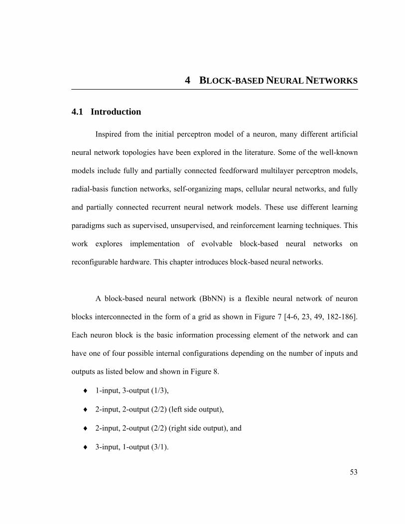
4 BLOCK-BASED NEURAL NETWORKS
4.1 Introduction
Inspired from the initial perceptron model of a neuron, many different artificial
neural network topologies have been explored in the literature. Some of the well-known
models include fully and partially connected feedforward multilayer perceptron models,
radial-basis function networks, self-organizing maps, cellular neural networks, and fully
and partially connected recurrent neural network models. These use different learning
paradigms such as supervised, unsupervised, and reinforcement learning techniques. This
work explores implementation of evolvable block-based neural networks on
reconfigurable hardware. This chapter introduces block-based neural networks.
A block-based neural network (BbNN) is a flexible neural network of neuron
blocks interconnected in the form of a grid as shown in Figure 7 [4-6, 23, 49, 182-186].
Each neuron block is the basic information processing element of the network and can
have one of four possible internal configurations depending on the number of inputs and
outputs as listed below and shown in Figure 8.
♦ 1-input, 3-output (1/3),
♦ 2-input, 2-output (2/2) (left side output),
♦ 2-input, 2-output (2/2) (right side output), and
♦ 3-input, 1-output (3/1).
53
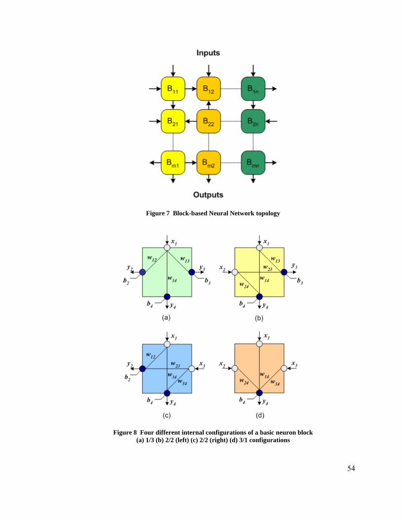
Figure 7 Block-based Neural Network topology
Figure 8 Four different internal configurations of a basic neuron block (a) 1/3 (b) 2/2 (left) (c) 2/2 (right) (d) 3/1 configurations
54
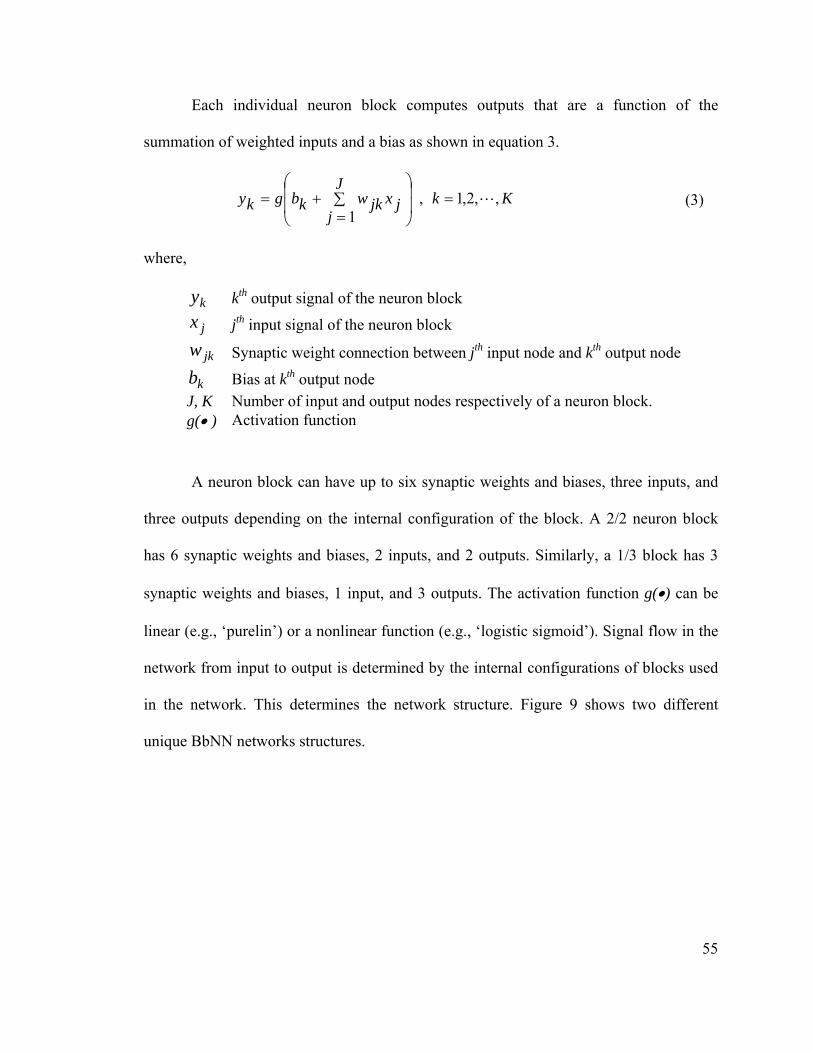
Each individual neuron block computes outputs that are a function of the
summation of weighted inputs and a bias as shown in equation 3.
KkJ
jjxjkwkbgky ,,2,1,
1L=⎟
⎟
⎠
⎞
⎜⎜
⎝
⎛∑=
+= (3)
where,
ky kth output signal of the neuron block
jx jth input signal of the neuron block
jkw Synaptic weight connection between jth input node and kth output node
kb Bias at kth output node J, K Number of input and output nodes respectively of a neuron block. g(• ) Activation function
A neuron block can have up to six synaptic weights and biases, three inputs, and
three outputs depending on the internal configuration of the block. A 2/2 neuron block
has 6 synaptic weights and biases, 2 inputs, and 2 outputs. Similarly, a 1/3 block has 3
synaptic weights and biases, 1 input, and 3 outputs. The activation function g(•) can be
linear (e.g., ‘purelin’) or a nonlinear function (e.g., ‘logistic sigmoid’). Signal flow in the
network from input to output is determined by the internal configurations of blocks used
in the network. This determines the network structure. Figure 9 shows two different
unique BbNN networks structures.
55
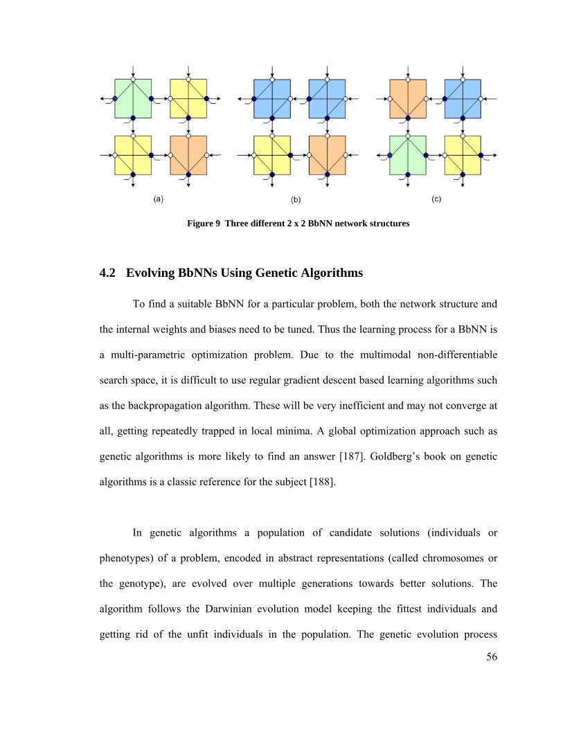
Figure 9 Three different 2 x 2 BbNN network structures
4.2 Evolving BbNNs Using Genetic Algorithms
To find a suitable BbNN for a particular problem, both the network structure and
the internal weights and biases need to be tuned. Thus the learning process for a BbNN is
a multi-parametric optimization problem. Due to the multimodal non-differentiable
search space, it is difficult to use regular gradient descent based learning algorithms such
as the backpropagation algorithm. These will be very inefficient and may not converge at
all, getting repeatedly trapped in local minima. A global optimization approach such as
genetic algorithms is more likely to find an answer [187]. Goldberg’s book on genetic
algorithms is a classic reference for the subject [188].
In genetic algorithms a population of candidate solutions (individuals or
phenotypes) of a problem, encoded in abstract representations (called chromosomes or
the genotype), are evolved over multiple generations towards better solutions. The
algorithm follows the Darwinian evolution model keeping the fittest individuals and
getting rid of the unfit individuals in the population. The genetic evolution process
56

57
involves selection of random (or biased random) individuals from the current population
for genetic crossover and mutation to produce the next generation. The selection strategy
used may be biased towards selecting individuals with higher fitness and use different
techniques such as the tournament selection or roulette wheel selection strategy. The
initial population is randomly initialized. A fitness function evaluates the fitness of every
individual in the population. With a biased selection strategy, individuals with higher
fitness are more likely to be selected for genetic reproduction (crossover and mutation) to
produce new populations. The fitness of newly generated individuals in the population is
evaluated using the fitness function and the evolution process proceeds, further producing
newer generations. The goal is to find an individual among the population with fitness
equal to or greater than the target fitness [188]. Figure 10 shows a flowchart for the
genetic evolution process described above.
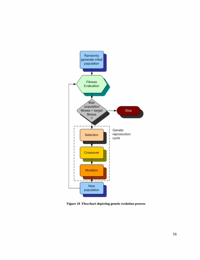
Figure 10 Flowchart depicting genetic evolution process
58

59
4.2.1 Genetic Operators
Operators in genetic algorithms are used to produce offspring to form new
generations. These are discussed in detail below.
4.2.1.1 Selection
Selection is a process in which a proportion of the existing population in each
successive generation is selected to breed a new generation. Individual solutions are
selected through a fitness-based process, where fitter solutions (as measured by a fitness
function) are typically more likely to be selected. The selection process is stochastic and
designed to also select a small proportion of less fit solutions to maintain population
diversity and prevent premature convergence of poor solutions. In tournament selection,
a group of randomly chosen individuals from the population are pitted against each other
and a winner (best fit individual) is selected for crossover. Selection pressure can be
adjusted by varying the tournament group size. In roulette wheel selection (also called
fitness proportionate selection); all the individuals in the population are ranked according
to their fitness, assigning each one a probability. The chance of an individual to be
selected is proportional to its rank. While candidate solutions with a lower fitness will be
more likely to be eliminated, there is still a chance that they may be selected.

60
4.2.1.2 Crossover
Crossover is a genetic process used to vary the programming of a chromosome(s)
from one generation to the next. It is analogous to biological crossover and reproduction.
Two parent chromosomes swap genetic information to produce two offspring. Many
crossover techniques exist such as one-point crossover, two-point crossover, and the cut
and splice strategy. For example, in a two-point crossover strategy if ‘S1=000000’ and
‘S2=111111’ are two chromosomes, then a crossover between the two using a randomly
selected crossover site (in this example after bit 2) could produce two offspring
‘S1’=110000’ and ‘S2’=001111’.
4.2.1.3 Mutation
In mutation, the bits of the candidate are randomly flipped based on some low
probability. The purpose is to maintain population diversity and induce a random walk
through the search space of possible solutions.
The genetic evolution process described above works well with a single
dimensional search space, but needs modification for multiparametric optimization
problems. The search space for our BbNN evolution problem poses a two-dimensional
optimization problem (simultaneous structure and weight optimization). Thus we need to
modify the genetic algorithm for it to work with the problem at hand. The learning
process uses a supervised training approach. The modified genetic algorithm is described
below.

61
4.2.2 BbNN Encoding
The structure and weight of the BbNN need to be encoded as a single
chromosome. The network structure is encoded as a gene using a sequence of binary
numbers representing the signal flow through the BbNN. Any connection between the
blocks is represented with either a binary 0 or a binary 1. A binary 0 denotes down (↓)
and left (←) signal flow directions, and a binary 1 indicates up (↑) and right (→) signal
flows. The number of bits required to represent the signal flow of an m × n BbNN is
‘(2m-1)n’. This is the case for a recurrent BbNN network where a signal flow from a
lower layer neuron block to an upper layer block (↑) is a valid network structure. In the
case of feedforward networks, a feedback as in the earlier case results in invalid
structures. Since the signal flow in feedforward neurons is restricted from top to bottom,
we do not need to encode that structure information as it is implied. Thus in a
feedforward network binary 0 denotes left (←) signal flow direction, and a binary 1
indicates right (→) signal flow. Thus the number of bits required to represent the signal
flow of an m × n block-based neural network is ‘mn’. Figure 11 illustrates recurrent
BbNN network structure encoding and Figure 12 shows a feedforward network structure
encoding. Synaptic connection weights of each neuron block in a network are encoded as
real values in an array. The arrays of all the blocks are concatenated sequentially to form
a weight gene. The weight gene along with the structure gene forms the BbNN
chromosome. Figure 13 shows the weight gene encoding and Figure 14 shows the
complete encoding of a BbNN chromosome for a 2 × 2 network.
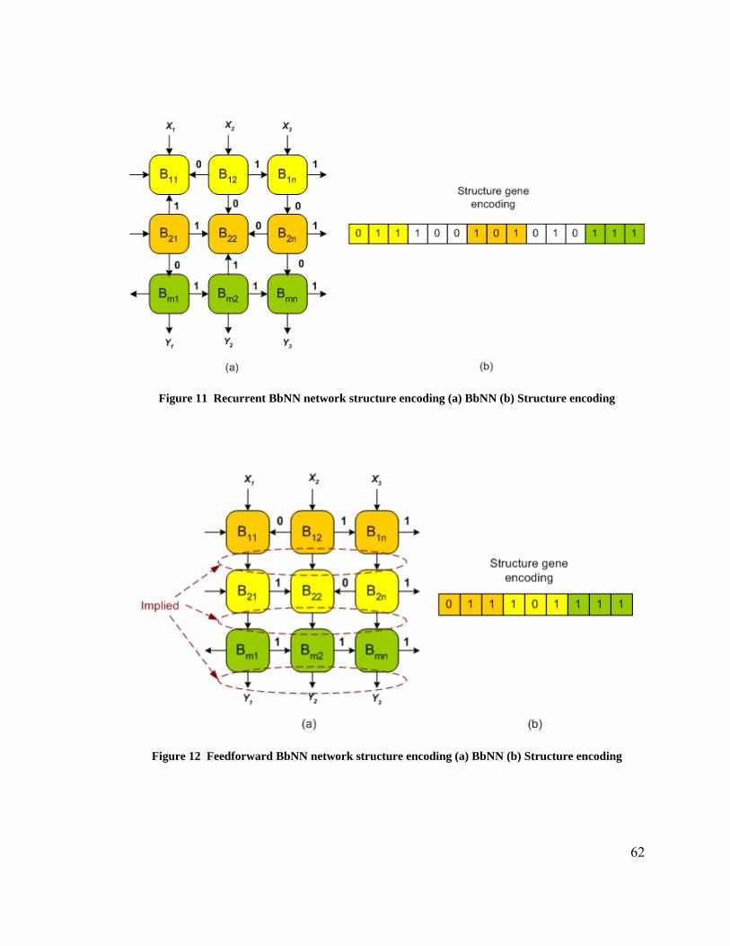
Figure 11 Recurrent BbNN network structure encoding (a) BbNN (b) Structure encoding
Figure 12 Feedforward BbNN network structure encoding (a) BbNN (b) Structure encoding
62
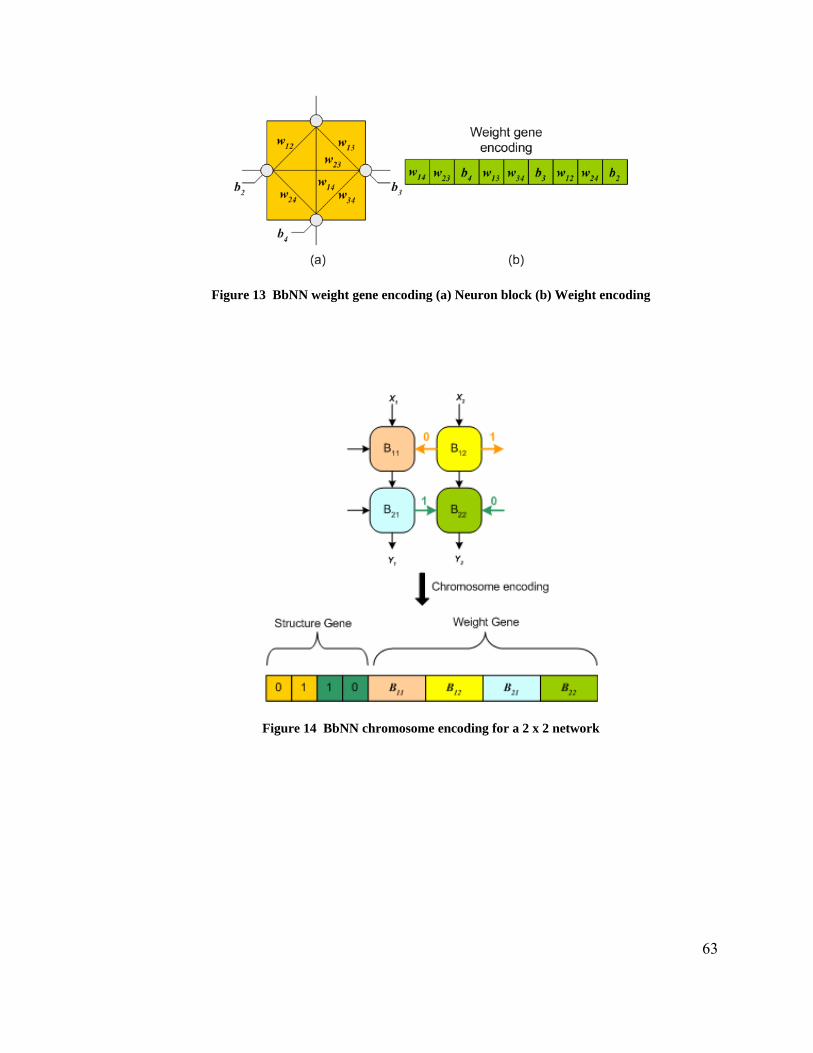
Figure 13 BbNN weight gene encoding (a) Neuron block (b) Weight encoding
Figure 14 BbNN chromosome encoding for a 2 x 2 network
63
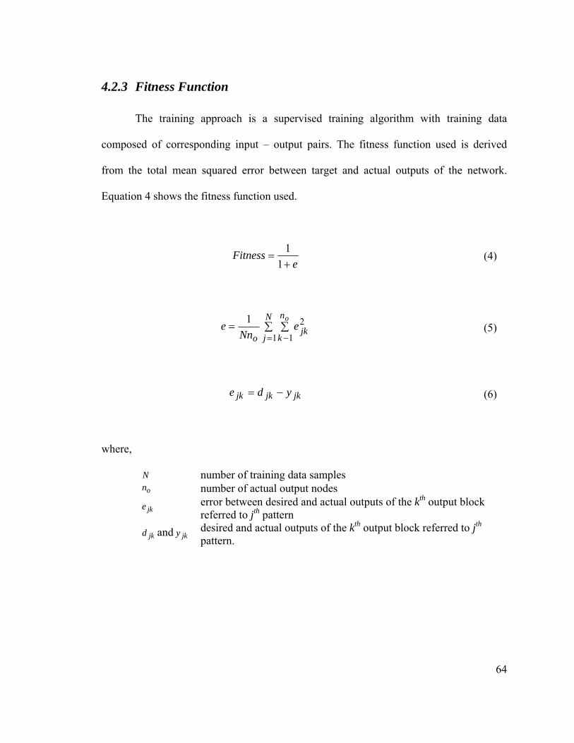
4.2.3 Fitness Function
The training approach is a supervised training algorithm with training data
composed of corresponding input – output pairs. The fitness function used is derived
from the total mean squared error between target and actual outputs of the network.
Equation 4 shows the fitness function used.
eFitness
+=
11 (4)
∑ ∑== −
N
j
n
kjk
o
oe
Nne
1 1
21 (5)
jkjkjk yde −= (6)
where,
N number of training data samples on number of actual output nodes
jke error between desired and actual outputs of the kth output block referred to jth pattern
jkd and jky desired and actual outputs of the kth output block referred to jth pattern.
64

65
4.2.4 Genetic Evolution
The 2-dimensional genetic evolution is similar to the one described above. A
population of BbNN chromosomes is randomly initialized and their fitness is evaluated.
A selection strategy (tournament or roulette wheel) selects individuals for genetic
crossover operations with selection pressure against the least fit individuals. The
crossover operator randomly swaps portions of the structure genes of the two parent
chromosomes based on a crossover probability. The offspring are added to the new
population. The mutation operator operates on the newly created individuals and has two
stages. First the structure mutation stage randomly flips structure gene bits based on a
low structure mutation probability. Second the weight mutation stage adds Gaussian
noise with zero mean and unit variance to the weights based on a low weight mutation
probability. The newly generated population is evaluated for fitness and the evolution
proceeds further with the new generation until an individual with fitness greater than or
equal to the target fitness is found or the maximum number of generations has been
reached. Figure 15 illustrates the structure crossover operation. The dotted lines shown in
the two parents are the structure crossover sites. The structure gene is sliced at these lines
and the sliced portions are swapped to produce two offspring as shown. Figure 16
illustrates the structure mutation operation in BbNNs. A bit is chosen randomly based on
a low mutation probability from the structure gene and flipped. The new structure gene
obtained and its corresponding BbNN network is shown in the figure.
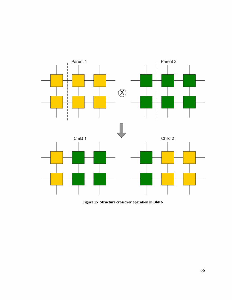
Figure 15 Structure crossover operation in BbNN
66
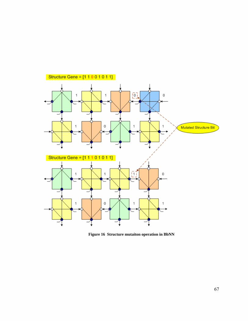
Figure 16 Structure mutaiton operation in BbNN
67
68
4.3 Summary
This chapter introduced BbNNs and multi-parametric genetic evolution algorithms
used to evolve the network structure and weights of the BbNNs. A BbNN is a network of
neuron blocks interconnected in the form of a grid. Due to the regular structure of these
networks they are well suited for custom implementations in digital hardware such as
field programmable gate arrays (FPGA) and application specific integrated circuits
(ASIC). Network structure regularity facilitates scaling the network in custom
implementations with ease. The internal configuration of the neuron blocks remains the
same (one out of the four described in section 4.1) as a result of scaling the network size.
The number of synaptic connections between the neuron blocks also grows linearly as a
result of scaling network size. This is unlike the popular multilayer perceptron (MLP)
networks. MLPs are fully connected networks of neurons with a synaptic connection
between each pair of neurons in the adjacent layers. Thus, growth in network size adds
many new synaptic connections to the network. Each new synaptic connection adds a
new stage to the multiplier and accumulator circuit of the neuron to which it serves as an
input. The multiplier and accumulator circuit in the neurons is used in calculating the
output which is a function of the weighted summation of the inputs and a bias. This
makes scaling the network structure difficult in hardware implementations for networks
such as MLPs. Thus, the regular network structure of BbNNs facilitates hardware
implementations. A disadvantage of the partial connectivity in network architectures such
as BbNNs is the possibility of requiring more equivalent neurons to solve the same
problems as would be required in the case of an MLP. The BbNNs can be trained using

69
genetic algorithms introduced in this chapter. The training is a multi-parametric
optimization problem involving simultaneous evolution of network structure and the
synaptic weights. Due to the multimodal non-differentiable search space it is difficult to
use regular gradient descent based learning algorithms such as the backpropagation
algorithm. These will be very inefficient and may not converge at all, getting repeatedly
trapped in local minima. A global optimization approach such as genetic algorithms is
more likely to find an answer [187]. But the disadvantage of using global training
approaches such as GA are longer training times than the directed gradient descent search
algorithms such as the backpropagation algorithm. Hybrid training algorithms for BbNNs
have been investigated that take the advantages of global sampling of GAs and fast
convergence of gradient descent techniques for efficient training of BbNNs. More
information on these can be found in [4, 5]. This dissertation uses the regular GA
approach presented in section 4.2. Moon and Kong proved that a BbNN of size m × n
can successfully represent the input – output characteristics of any MLP network for n ≤
5 [23]. BbNNs have been applied to mobile robot navigation [23], multivariate gaussian
distributed pattern classification [182], chaotic time series prediction [183], and ECG
signal classification [4-6].
5 INTRINSICALLY EVOLVABLE BBNN PLATFORM
Many custom artificial neural network implementations have been reported in
hardware. Section 2.5 presents a review of these implementations. Most implementations
rely on an offline neural network learning in software simulations, with the resultant
network being custom-built either in fixed ASICs or reconfigurable FPGAs. Thus, only
the recall stage benefits from custom implementation speedups. Every new application of
these networks needs a new custom design built and configured on the FPGAs or ASICs.
The design goal here is to build an online neural network learning platform that can be
trained and adapted intrinsically in hardware. This platform is an intrinsically evolvable
hardware system performing functional-level evolution. The evolving functional modules
and their interconnections are artificial neurons and their synaptic connections. The
neural network implemented is the feedforward block-based neural network (BbNN)
discussed in chapter 4. The following sections give the design details for the BbNN
platform.
5.1 BbNN FPGA Design Details
The design was implemented for a Xilinx Virtex-II Pro (XC2VP30) FPGA [189]
housed on a Xilinx University Program (XUP) FPGA development board [190] or an
Amirix AP130 FPGA development board [191]. This particular FPGA includes 2 on-chip
PowerPC 405 embedded processor cores, 30,816 logic cells, 136 built-in 18x18
70
71
multipliers, and 2448 KBits (306 KBytes) of on-chip block RAM. These multipliers will
be used to build the multiplier and accumulate circuits in the FPGA units for neuron
block processing and the available on-chip block RAM will be used to store the
activation functions. The PowerPC will be used for the genetic algorithm and control
operations in our design. These will be discussed in details in section 5.1.
For on-chip learning the network design has to be flexible to accommodate
dynamic changes in network structure and internal parameters (synaptic weights and
biases). As discussed in section 2.5.2.2 the time taken for each FPGA reconfiguration
cycle is on the order of milliseconds. This poses a bottleneck for an online evolution
system that relies heavily on FPGA reconfigurations for changes in network structure and
internal parameters. Thus we need to minimize any reconfiguration cycles that would be
required during the learning stage for better performance. In the case of BbNNs, the
following dynamic updates have to be accommodated for an on-chip learning capability.
♦ Dynamic updates to network structure
Network structure and internal configurations of neuron blocks is dictated
by the structure gene. Any change in the structure gene changes the internal
configurations of the neuron blocks in the grid, thus modifying the dataflow
through the network. To accommodate this dynamically, we need a neuron block
design that can dynamically emulate any of the four internal configuration modes
without requiring an FPGA reconfiguration.

72
♦ Addition/deletion of row(s) / column(s)
The genetic evolution process could potentially add / delete rows and
columns to / from the BbNN grid. Accordingly, it either increases or shortens the
length of the structure and weight genes in the BbNN chromosome. From the
hardware design perspective, any addition of a row or column to the existing
network grid adds new neuron blocks and a few new nets (connections) between
the old and new neuron blocks. This is difficult to accommodate dynamically in
FPGAs and may require a reconfiguration cycle. The design presented here
minimizes the overhead of reconfiguration cycles as will be evident from the
design of the neuron block and the dataflow architecture.
♦ Dynamic updates to synaptic weights and biases
Synaptic weights and biases are stored in digital registers and can be
dynamically updated without requiring any FPGA reconfigurations.
Other requirements and considerations for the design include the following.
♦ Data representation and precision
♦ Activation function implementation
♦ Internal neuron block configurations
♦ Dataflow implementation
♦ Area, speed, and power
♦ Design scalability and real-time processing support
73
These design considerations and the resulting decisions are discussed below.
5.1.1 Data Representation and Precision
The inputs, outputs, and internal parameters such as synaptic weights and biases
are all real-valued variables. Representing and storing them in digital hardware can be
either done using floating point or fixed point number representation. Floating point
representation will have a significantly wider range and higher precision as compared to
fixed point representations. However, floating point arithmetic circuits are complicated to
build, have much larger footprint in silicon, and our significantly slower as compared to
those required for fixed point arithmetic. Our design is targeting FPGA devices. The
device capacities of current generation FPGAs are significantly smaller as compared to
comparable ASICs. Building custom or single precision floating point arithmetic circuits
has started becoming feasible with the device capacities of current generation FPGAs
[192-195]. To be able to fit as many neuron blocks as possible on a single FPGA chip,
the area occupied by each block should be as small as possible. Holt and Baker [44] and
Holt and Hwang [45] investigated the minimum precision problem for neural networks
with benchmark classification problems. According to their analysis, 16 bit fixed-point
representation is sufficient for correct classification and training of the neural networks.
Also, in our analysis of the applications considered here 16 bit precision is sufficient.
Thus, all the internal parameters as well as inputs and outputs are represented as 16 bit
fixed point numbers.
74
5.1.2 Activation Function Implementation
Activation functions are typically non-linear monotonically increasing sigmoid
functions. Implementation choices include a circuit implementation for a piece-wise
linear approximation of the function versus implementing a lookup table with preloaded
f(x) values for the corresponding x input value. Direct circuit implementations of the
activation function are significantly smaller in silicon footprint as compared to the LUT
approach. The size of the LUT increases exponentially with the size of input. However,
the direct circuit implementations are more complicated to design and may require
redesign for each different activation function. In the case of an LUT-based approach,
new values can be reloaded for a different activation function when required during the
on-chip training process. As for the disadvantage of the required silicon area, the LUTs
were implemented using the block RAMs in the Xilinx FPGAs. Since these block RAMs
are already present on the die as hard-macros whether they are used or not, it made sense
to use them to our advantage. Thus, minimal reconfigurable logic resources are used for
activation function implementation. Port A of the on-chip dual port block RAM is
configured as a read/write port. It is used to load the values into the lookup table. Port B
is configured as a read only port and is used to interface with the neuron blocks. The size
of the lookup table required is directly associated with the data widths used. A 16-bit
fixed point representation requires a LUT that is 16 bits wide and 216 deep. This requires
a total of 128 KBytes per LUT. It would be desirable to use a separate LUT for every
neuron block in the network so that all the neuron blocks are completely independent of
each other. However, using a separate LUT for every neuron block can severely limit the
number of blocks that can be implemented on a single FPGA chip. In our case, we can
75
implement only 2 neuron blocks on the Xilinx XC2VP30 FPGA chip before we run out
of block RAMs. Sharing the LUT between all the neuron blocks requires serializing the
access to the LUT of the neuron blocks using a FIFO, consequently slowing down the
computational speed. Keeping in mind the dataflow implementation technique used here,
only one neuron block in a column can ‘fire’ (process input data and producing outputs)
in any computational time unit (this will be explained in further detail in the dataflow
implementation section). Hence, a design decision was made to share a LUT between
neuron blocks in a single column instead of all the blocks in the network. Thus there will
be one LUT per column of neuron blocks in the network. This choice does increase the
number of blocks that we can use in the network, but puts a constraint on the number of
columns that can be implemented before the available block RAM become a bottleneck.
The number of columns that can be implemented on our current FPGA chip would still
be just two columns, severely limiting the network ability to solve any interesting
problems. So, to further optimize the size of the LUT so that larger network grid sizes can
be implemented on our FPGA chip, we implemented a LUT that was 16 bits wide but
only 212 deep. This reduces the size of the LUT to 8 Kbytes per LUT. This was done
taking into consideration an observation that almost all of the activation functions that are
used for artificial neurons are monotonically increasing saturating functions such as
hyperbolic tangent and the logistic sigmoid functions. That is, the outputs taper off to a
constant value beyond a certain input value. Thus there is no need to store the values
greater than the maximum saturated output value repeatedly, in effect chopping off the
activation function beyond the saturated values. Hence, the number of LUTs and hence
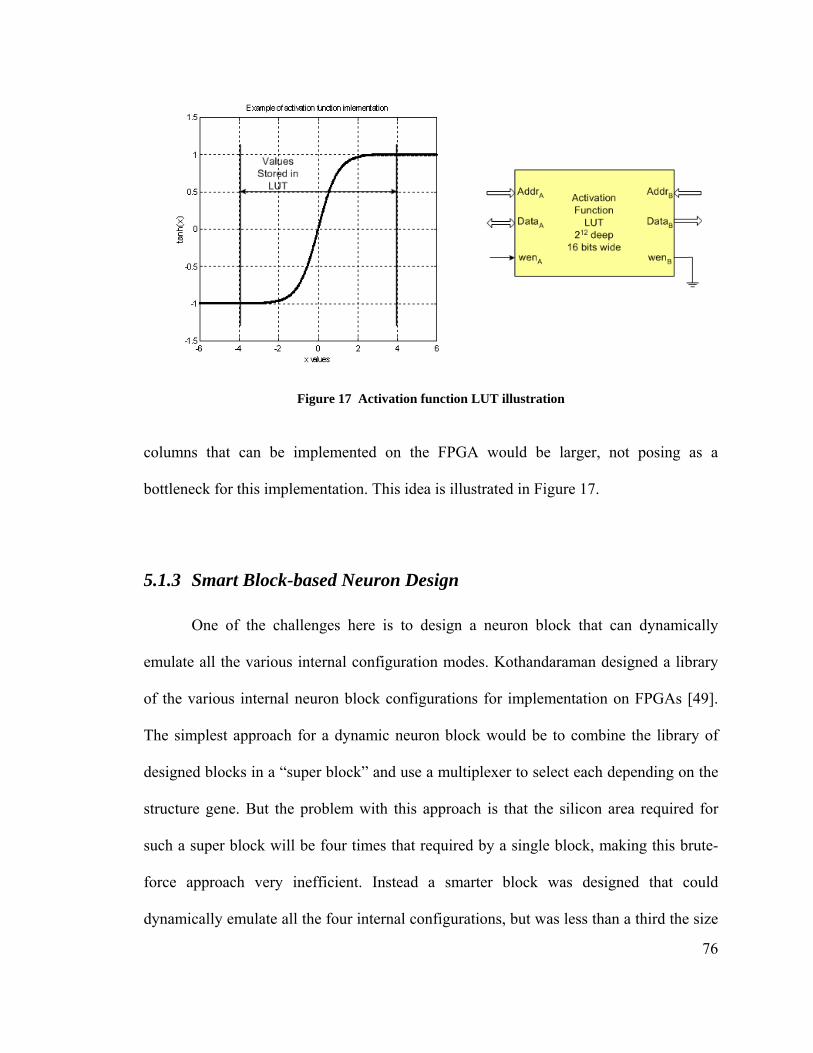
Figure 17 Activation function LUT illustration
76
columns that can be implemented on the FPGA would be larger, not posing as a
bottleneck for this implementation. This idea is illustrated in Figure 17.
5.1.3 Smart Block-based Neuron Design
One of the challenges here is to design a neuron block that can dynamically
emulate all the various internal configuration modes. Kothandaraman designed a library
of the various internal neuron block configurations for implementation on FPGAs [49].
The simplest approach for a dynamic neuron block would be to combine the library of
designed blocks in a “super block” and use a multiplexer to select each depending on the
structure gene. But the problem with this approach is that the silicon area required for
such a super block will be four times that required by a single block, making this brute-
force approach very inefficient. Instead a smarter block was designed that could
dynamically emulate all the four internal configurations, but was less than a third the size
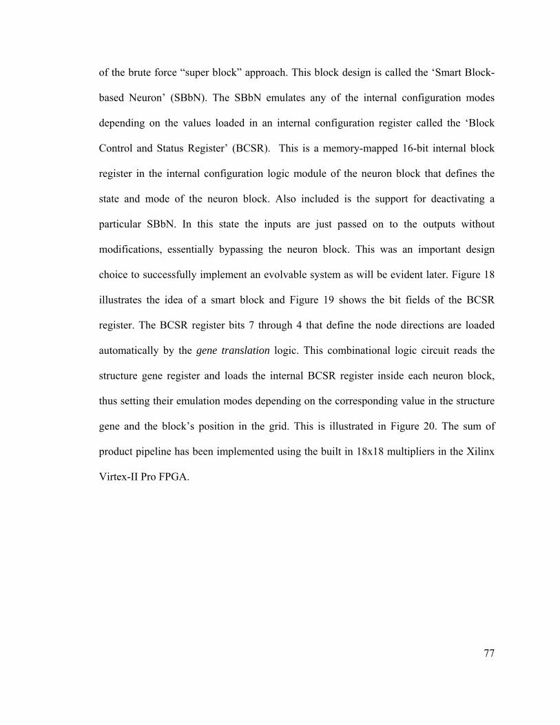
77
of the brute force “super block” approach. This block design is called the ‘Smart Block-
based Neuron’ (SBbN). The SBbN emulates any of the internal configuration modes
depending on the values loaded in an internal configuration register called the ‘Block
Control and Status Register’ (BCSR). This is a memory-mapped 16-bit internal block
register in the internal configuration logic module of the neuron block that defines the
state and mode of the neuron block. Also included is the support for deactivating a
particular SBbN. In this state the inputs are just passed on to the outputs without
modifications, essentially bypassing the neuron block. This was an important design
choice to successfully implement an evolvable system as will be evident later. Figure 18
illustrates the idea of a smart block and Figure 19 shows the bit fields of the BCSR
register. The BCSR register bits 7 through 4 that define the node directions are loaded
automatically by the gene translation logic. This combinational logic circuit reads the
structure gene register and loads the internal BCSR register inside each neuron block,
thus setting their emulation modes depending on the corresponding value in the structure
gene and the block’s position in the grid. This is illustrated in Figure 20. The sum of
product pipeline has been implemented using the built in 18x18 multipliers in the Xilinx
Virtex-II Pro FPGA.
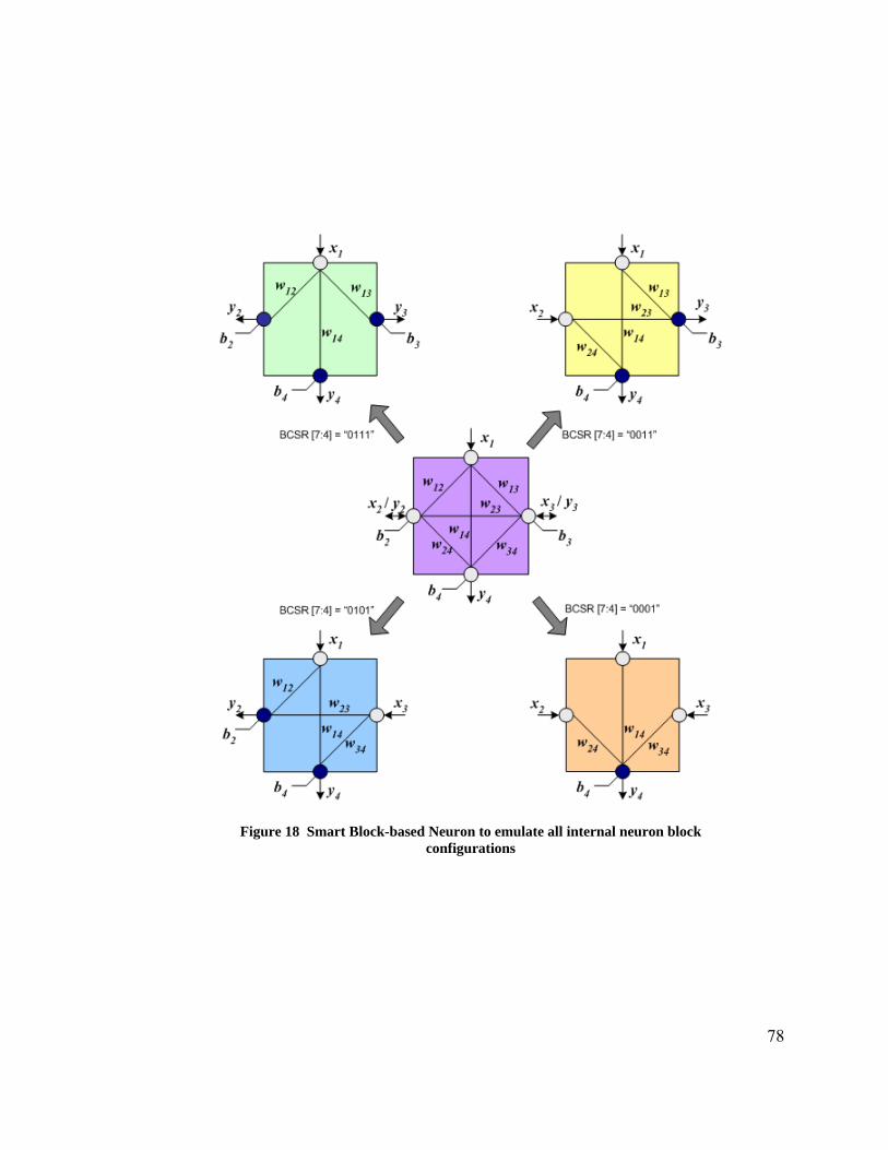
Figure 18 Smart Block-based Neuron to emulate all internal neuron block configurations
78
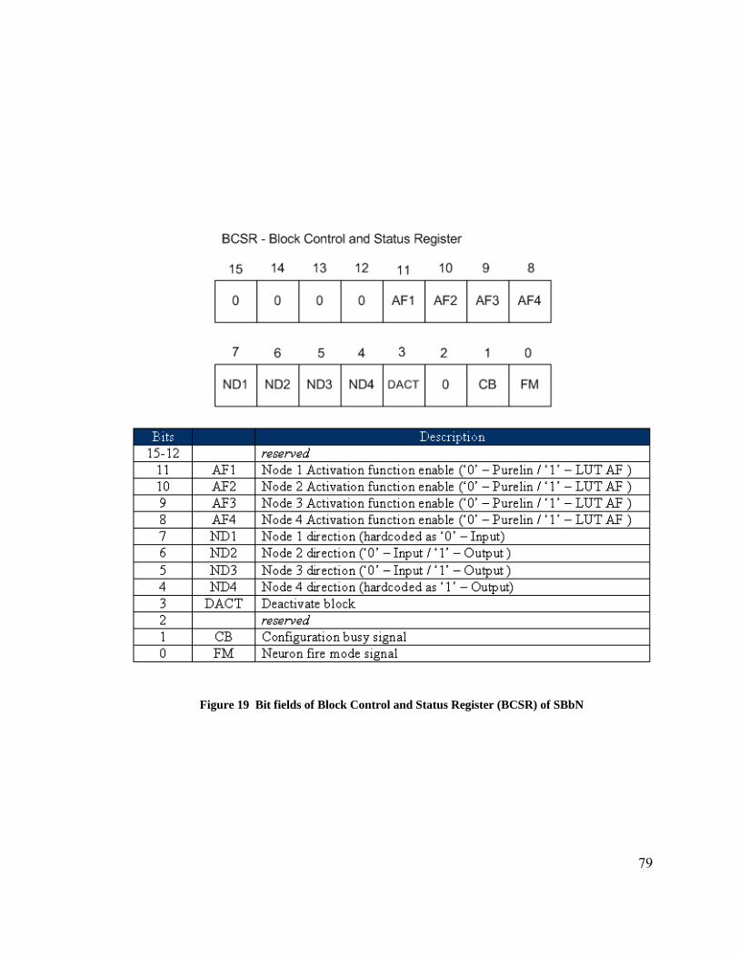
Figure 19 Bit fields of Block Control and Status Register (BCSR) of SBbN
79
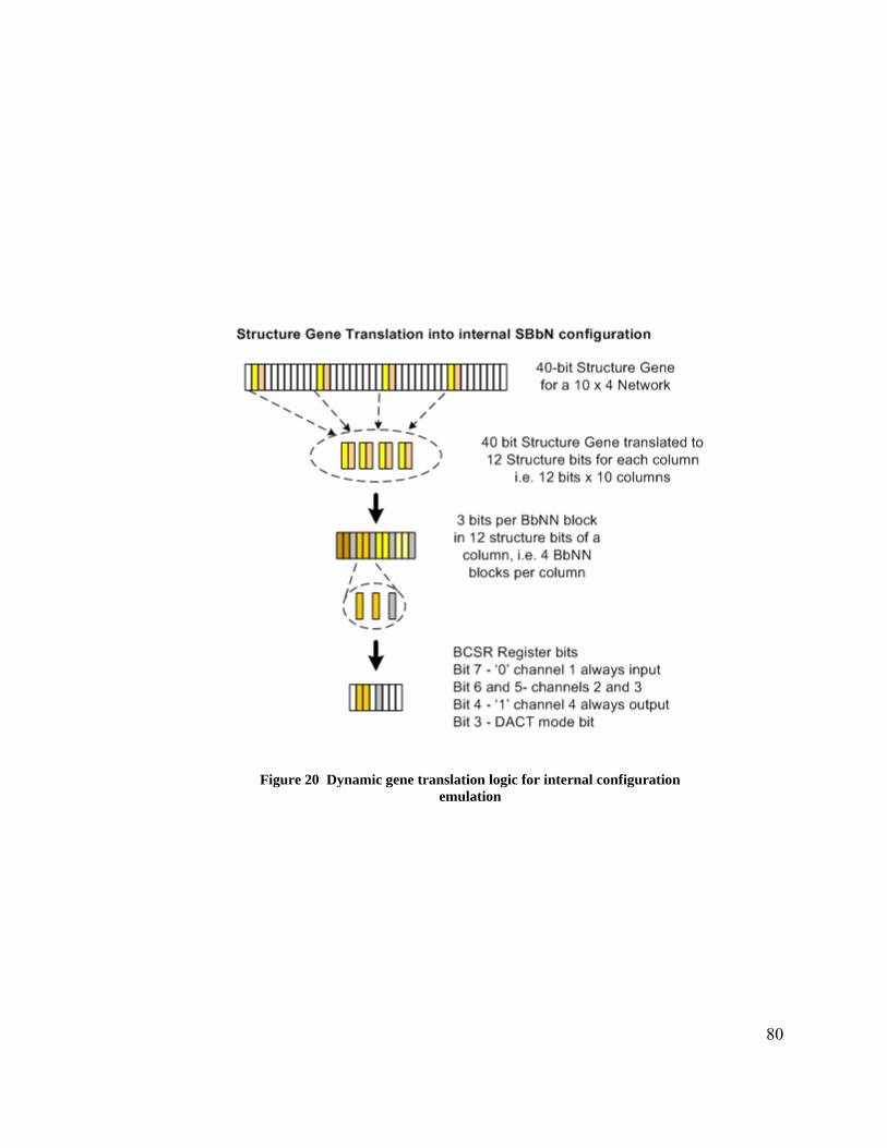
Figure 20 Dynamic gene translation logic for internal configuration emulation
80
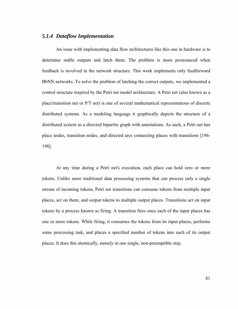
81
5.1.4 Dataflow Implementation
An issue with implementing data flow architectures like this one in hardware is to
determine stable outputs and latch them. The problem is more pronounced when
feedback is involved in the network structure. This work implements only feedforward
BbNN networks. To solve the problem of latching the correct outputs, we implemented a
control structure inspired by the Petri net model architecture. A Petri net (also known as a
place/transition net or P/T net) is one of several mathematical representations of discrete
distributed systems. As a modeling language it graphically depicts the structure of a
distributed system as a directed bipartite graph with annotations. As such, a Petri net has
place nodes, transition nodes, and directed arcs connecting places with transitions [196-
198].
At any time during a Petri net's execution, each place can hold zero or more
tokens. Unlike more traditional data processing systems that can process only a single
stream of incoming tokens, Petri net transitions can consume tokens from multiple input
places, act on them, and output tokens to multiple output places. Transitions act on input
tokens by a process known as firing. A transition fires once each of the input places has
one or more tokens. While firing, it consumes the tokens from its input places, performs
some processing task, and places a specified number of tokens into each of its output
places. It does this atomically, namely in one single, non-preemptible step.

82
The BbNN dataflow can be represented using an acyclic Petri net. Each of the
blocks can be represented by an equivalent Petri net model as shown in Figure 21. The
input and output registers can be represented by places. When each of the input registers
(input places) have a valid input (a token), the BbNN fires and computes the outputs.
Each of the output places will now get a token after the BbNN fires and the tokens at the
input places are consumed. Thus the dataflow through a BbNN network can be
represented using an equivalent Petri net network model (replacing each block with
equivalent Petri net model as shown in Figure 21) for the entire BbNN network structure.
Figure 22 shows the firing sequence for a particular BbNN network example. The side
inputs have been hard-coded to be zero and have a valid token (shown as a ‘●’) until
consumed by firing. When the top inputs are applied the input places get tokens and they
fire, computing the outputs. As can be seen, only the blocks with valid input tokens fire
and generate the corresponding input tokens for the neighbors, which in turn fire next.
Figure 23 shows a logical block diagram of a SBbN block.
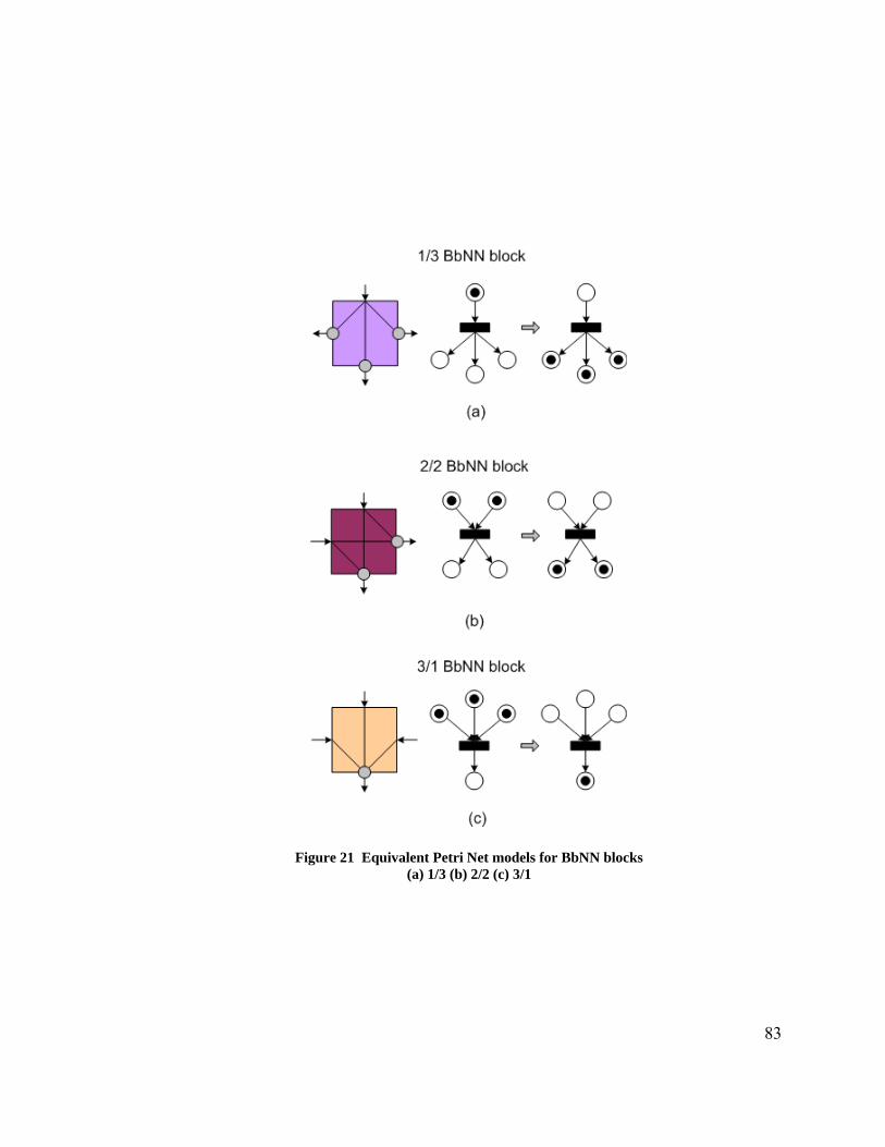
Figure 21 Equivalent Petri Net models for BbNN blocks (a) 1/3 (b) 2/2 (c) 3/1
83
Figure 22 An example 2 x 2 BbNN firing sequence
84
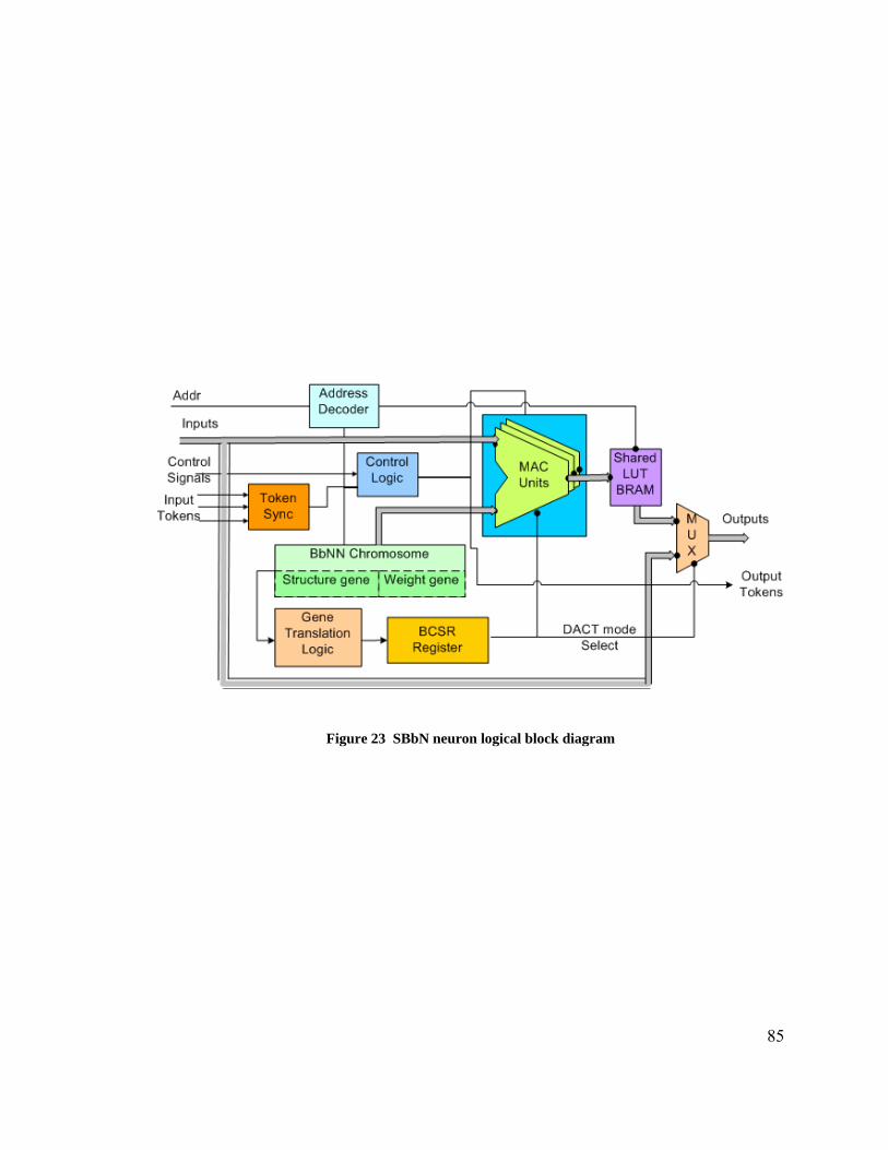
Figure 23 SBbN neuron logical block diagram
85
86
5.2 Embedded Intrinsically Evolvable Platform
Block-based neural networks are evolved using genetic algorithms to find a
suitable network for input – output mapping of training data. The details of the genetic
evolution process are described in section 4.2. Section 5.1 gives details on the digital
hardware design of the block-based neural network. The structure and internal parameters
of the designed network can be dynamically updated without relying on FPGA runtime
reconfigurations. The design is implemented on Xilinx Virtex-II Pro FPGA development
boards. The implementation goal is to design an embedded, intrinsically evolvable
platform for online evolution of BbNNs. This requires close coupling of the genetic
evolution algorithm with the designed network. Multiple design choices were carefully
considered for implementation, the details of which are given below.
a) Implementing Genetic Algorithms on a Host Computer
Here the GA is implemented as a software program running on a host computer
that communicates with an FPGA configured with the neural network hardware via a
serial link or bus interface such as PCI. The fitness evaluation is done on the FPGA
configured with the hardware design of BbNNs. The problem with this choice is that the
system is difficult to deploy as a standalone embedded system and would be bulky if
implemented with embedded single board computers.
87
b) Implementing Genetic Algorithms in Hardware
Implementing GAs in hardware along with the BbNN network was the most
obvious choice. Hardware implementations of different flavors of compact GAs have
been reported in the literature [161, 162, 167, 168, 199], but it comes at a cost of
significant resources on the FPGA. An on-chip GA implementation would require a
memory bank to hold the population of chromosomes. It will also require a Gaussian
random number generator implementation for mutation operation which again will
require a memory bank to store lookup table values for a compact implementation using a
uniform random number generator or a large logic implementation [200]. These required
memory banks can be implemented in internal block RAMs available in the Virtex-II Pro
FPGAs, but most of the block RAMs are tied up activation function LUT
implementation. Building memory out of the rest of the reconfigurable fabric would be
area inefficient and the resulting circuit slower limiting the size and performance of
ANNs that can be implemented in hardware.
c) Implementing Genetic Algorithms on Embedded PPC405
Another choice is an approach similar to the first one, where the GA evolution is
done in software running on a host processor. But in this case, the processor is an
embedded processor on-chip in the Virtex-II Pro FPGA. The fitness evaluation, the most
time consuming computation, is still implemented in the FPGA reconfigurable fabric.
The advantage of this approach is that it uses the on-chip, embedded PowerPC 405
processor located on the same die as the rest of the reconfigurable fabric in the Virtex-II
Pro FPGA. Thus, the system can be deployed as a compact, embedded, evolvable
88
platform in real-world applications. The fitness evaluation, which is the bottleneck in GA
evolution strategy discussed here, is accelerated using the custom logic circuitry in the
FPGA.
After comparing the pros and cons of the above approaches it was decided to
implement the GA evolution on the PowerPC 405 embedded processor.
5.2.1 PSoC Platform Design
The BbNN platform was developed as a programmable System On-Chip (PSoC)
architecture. Taking advantage of increased chip capacities, current-generation FPGAs
have a number of on-chip hard macros such as embedded processors, memory,
multipliers, and accumulator units. These available hard / soft cores with synthesizable
local and peripheral bus systems can be used to build a powerful design platform on a
single chip. These systems include one or more hard/soft processors and the associated
local and peripheral bus systems with connected peripheral I/O cores on a single die. This
platform is aptly called a System on a Chip (SoC). These platforms synthesized on
FPGAs can be reconfigured and hence are called as programmable SoC (PSoC)
architectures. The embedded processors use internal FPGA RAMs for implementing
instruction and data memories. The embedded processor interfaces to on-chip memory
controllers via a local system bus. Peripherals like UART, ethernet MACs and other
custom user cores communicate with the processor via the local system bus or the
peripheral bus. The peripheral bus communicates with the local system bus via a bridge.
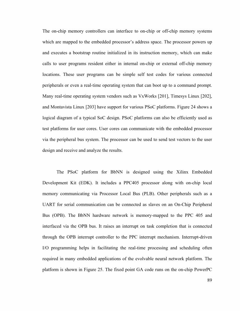
89
The on-chip memory controllers can interface to on-chip or off-chip memory systems
which are mapped to the embedded processor’s address space. The processor powers up
and executes a bootstrap routine initialized in its instruction memory, which can make
calls to user programs resident either in internal on-chip or external off-chip memory
locations. These user programs can be simple self test codes for various connected
peripherals or even a real-time operating system that can boot up to a command prompt.
Many real-time operating system vendors such as VxWorks [201], Timesys Linux [202],
and Montavista Linux [203] have support for various PSoC platforms. Figure 24 shows a
logical diagram of a typical SoC design. PSoC platforms can also be efficiently used as
test platforms for user cores. User cores can communicate with the embedded processor
via the peripheral bus system. The processor can be used to send test vectors to the user
design and receive and analyze the results.
The PSoC platform for BbNN is designed using the Xilinx Embedded
Development Kit (EDK). It includes a PPC405 processor along with on-chip local
memory communicating via Processor Local Bus (PLB). Other peripherals such as a
UART for serial communication can be connected as slaves on an On-Chip Peripheral
Bus (OPB). The BbNN hardware network is memory-mapped to the PPC 405 and
interfaced via the OPB bus. It raises an interrupt on task completion that is connected
through the OPB interrupt controller to the PPC interrupt mechanism. Interrupt-driven
I/O programming helps in facilitating the real-time processing and scheduling often
required in many embedded applications of the evolvable neural network platform. The
platform is shown in Figure 25. The fixed point GA code runs on the on-chip PowerPC
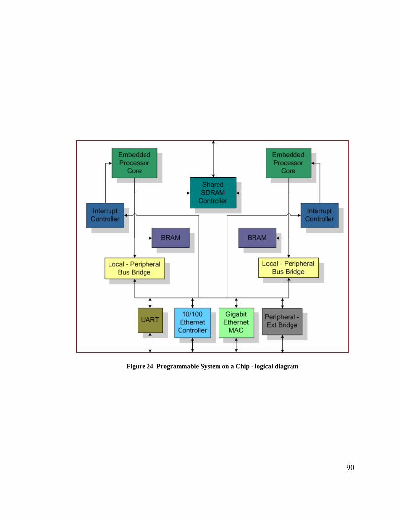
Figure 24 Programmable System on a Chip - logical diagram
90
Figure 25 BbNN PSoC platform. GA operators execute on PPC405, Fitness evaluation done using hardware BbNN design
processor. The BbNN hardware design is used for fitness evaluation. Internal network
parameters, such as the structure and weight genes, network inputs, and outputs are
memory-mapped to the processor. The activation function LUT also is memory mapped
in the address space of the PPC405.
5.3 Fixed Point BbNN Software for Genetic Evolution
The fixed point GA evolution software is written in the C programming language.
The on-chip PPC405 only has a fixed point datapath. Any floating point operations have
to be performed using emulated floating point software libraries which are slow. Care has
been taken to minimize the required floating point operations. All the real values have
been stored as 16-bit fixed point values. The genetic operators of selection, crossover,
and mutation have been implemented as detailed in chapter 4. Genetic evolution
91
92
parameters such as the maximum number of generations, structure / weight crossover and
mutation probabilities, step size for weight mutation, target fitness, elitist mode genetic
evolution selection, number of offspring in each new generation, activation function
selection (tansig, logsig, satlin, purelin, hardlim), selection algorithm (roulette, ranking,
tournament, proportion), and network grid sizes to evaluate can be set in a header file.
The software is cross-compiled to PPC 405 object code and can be loaded in the onboard
program flash. Fixed point BbNN fitness evaluation software routines have also been
programmed for use in a fixed point BbNN software simulator compiled for PC. These
routines also help in exhaustive BbNN FPGA design testing. The code appears in the
appendix.
5.4 Performance and Device Utilization Summary
The post-synthesis timing analysis of the design reports a clock frequency of
245MHz on the Xilinx Virtex-II Pro FPGA (XC2VP30). Each block takes at the most 10
CLK cycles to complete processing the inputs and produce an output. The number of
clock cycles depends on the internal block configuration and the number of output nodes
using the activation function LUT. Each block computation processes 6 synaptic
connections. Thus, each block has a peak connection per second speed of 147 MCPS per
block for a 16 bit data width. With generally more than one block computing at a time,
depending on the network structure the peak CPS would be (n computing blocks)×(147
MCPS / block) processing speed. Considering an m×n BbNN grid the processing speed
can vary between 147 MCPS to 147n MCPS, depending on the network structure.
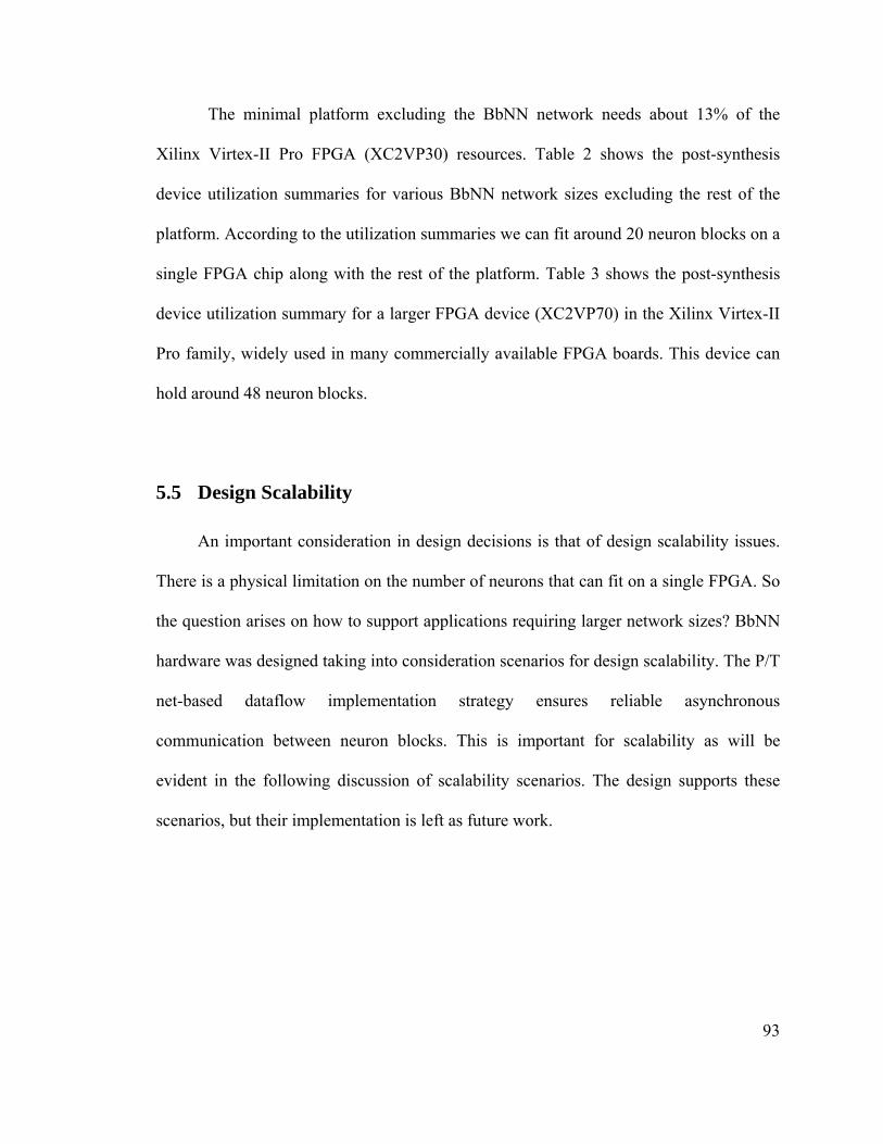
93
The minimal platform excluding the BbNN network needs about 13% of the
Xilinx Virtex-II Pro FPGA (XC2VP30) resources. Table 2 shows the post-synthesis
device utilization summaries for various BbNN network sizes excluding the rest of the
platform. According to the utilization summaries we can fit around 20 neuron blocks on a
single FPGA chip along with the rest of the platform. Table 3 shows the post-synthesis
device utilization summary for a larger FPGA device (XC2VP70) in the Xilinx Virtex-II
Pro family, widely used in many commercially available FPGA boards. This device can
hold around 48 neuron blocks.
5.5 Design Scalability
An important consideration in design decisions is that of design scalability issues.
There is a physical limitation on the number of neurons that can fit on a single FPGA. So
the question arises on how to support applications requiring larger network sizes? BbNN
hardware was designed taking into consideration scenarios for design scalability. The P/T
net-based dataflow implementation strategy ensures reliable asynchronous
communication between neuron blocks. This is important for scalability as will be
evident in the following discussion of scalability scenarios. The design supports these
scenarios, but their implementation is left as future work.
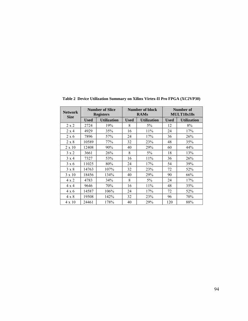
94
Table 2 Device Utilization Summary on Xilinx Virtex-II Pro FPGA (XC2VP30)
Number of Slice Registers
Number of block RAMs
Number of MULT18x18s Network
Size Used Utilization Used Utilization Used Utilization
2 x 2 2724 19% 8 5% 12 8% 2 x 4 4929 35% 16 11% 24 17% 2 x 6 7896 57% 24 17% 36 26% 2 x 8 10589 77% 32 23% 48 35%
2 x 10 12408 90% 40 29% 60 44% 3 x 2 3661 26% 8 5% 18 13% 3 x 4 7327 53% 16 11% 36 26% 3 x 6 11025 80% 24 17% 54 39% 3 x 8 14763 107% 32 23% 72 52%
3 x 10 18456 134% 40 29% 90 66% 4 x 2 4783 34% 8 5% 24 17% 4 x 4 9646 70% 16 11% 48 35% 4 x 6 14587 106% 24 17% 72 52% 4 x 8 19508 142% 32 23% 96 70%
4 x 10 24461 178% 40 29% 120 88%
95
Table 3 Device Utilization Summary on Xilinx Virtex-II Pro FPGA (XC2VP70)
Number of Slice Registers
Number of block RAMs
Number of MULT18x18s Network
Size Used Utilization Used Utilization Used Utilization
2 x 2 2497 7% 8 2% 12 3% 2 x 4 4929 14% 16 4% 24 7% 2 x 6 7390 22% 24 7% 36 10% 2 x 8 9915 29% 32 9% 48 14%
2 x 10 12403 37% 40 12% 60 18% 3 x 2 3661 11% 8 2% 18 5% 3 x 4 7327 22% 16 4% 36 10% 3 x 6 11025 33% 24 7% 54 16% 3 x 8 14788 44% 32 39% 72 9%
3 x 10 18461 55% 40 12% 90 27% 3 x 12 22233 67% 48 14% 108 33% 3 x 14 25652 77% 56 17% 126 38% 3 x 16 29254 88% 64 19% 144 43% 4 x 2 4783 14% 8 2% 24 7% 4 x 4 9646 29% 16 4% 48 14% 4 x 6 14561 44% 24 7% 72 21% 4 x 8 19534 59% 32 9% 96 29%
4 x 10 24470 73% 40 12% 120 36% 4 x 12 29221 88% 48 14% 144 43% 4 x 14 34389 103% 56 17% 168 51%
96
5.5.1 Scaling BbNN Across Multiple FPGAs
An obvious choice to scale the network sizes is to distribute smaller sub-networks
of the BbNN network across multiple FPGAs to execute in parallel. But this is not trivial
to achieve due to the inter-neuron block synaptic communications within the network.
These communications will have to be performed across multiple FPGA chips. This will
require taking into consideration delay times associated with the communication links
between the FPGAs. The FPGAs could be connected directly via dedicated inter-
communication channels or may have to go through the host processor and use
communication links such as Ethernet existing between the host machines. These issues
were considered during the design stage of the BbNN hardware implementation. The
choice of using the P/T net-based reliable, asynchronous inter-neuron block
communication was made to address the scalability issues. Asynchronous communication
ensures reliable performance irrespective of the delays associated with the
communication links. This makes the design portable and scalable across a heterogeneous
mixture of reconfigurable computing resources and their intercommunication channels.
5.5.2 Scaling via Time Folding
BbNNs can also be scaled via time-multiplexing. A single BbNN FPGA
implementation can be used to execute sub-networks of a larger BbNN at different
instances of time. The intermediate sub-network states (intermediate inputs and outputs
of the sub-network, sub-network structure, and internal parameters) can be saved in
buffer memory between the execution cycles. The intermediate sub-network states saved
97
in the buffer memory can be loaded on the BbNN FPGA implementation in appropriate
execution cycles to compute sub-network outputs that are input to other sub-networks.
Scaling the BbNN in time has the disadvantage of serializing the sub-network execution.
Thus, it requires longer execution times but lesser hardware resources.
5.5.3 Hybrid Implementation
A hybrid approach employing both time and space scaling techniques can also be
used for large networks. It is a problem of reliably mapping and scheduling sub-networks
across FPGA resources. It involves development of efficient partitioning and scheduling
algorithms for optimal usage of available resources and minimizing execution runtimes.
5.6 Applications
BbNNs can be applied to many applications suitable for neural networks. We
tested our on-chip training approach with a few example applications and the results are
discussed below.
5.6.1 N-bit Parity Classifier
A parity bit is a binary bit that indicates whether the number of bits with value of
one in a given set of N-bits is even or odd. The N-bit parity technique is widely used for
error detection in real world applications such as serial data transmission, SCSI bus,
microprocessor caches, and redundant arrays of inexpensive disks (RAID). The BbNN
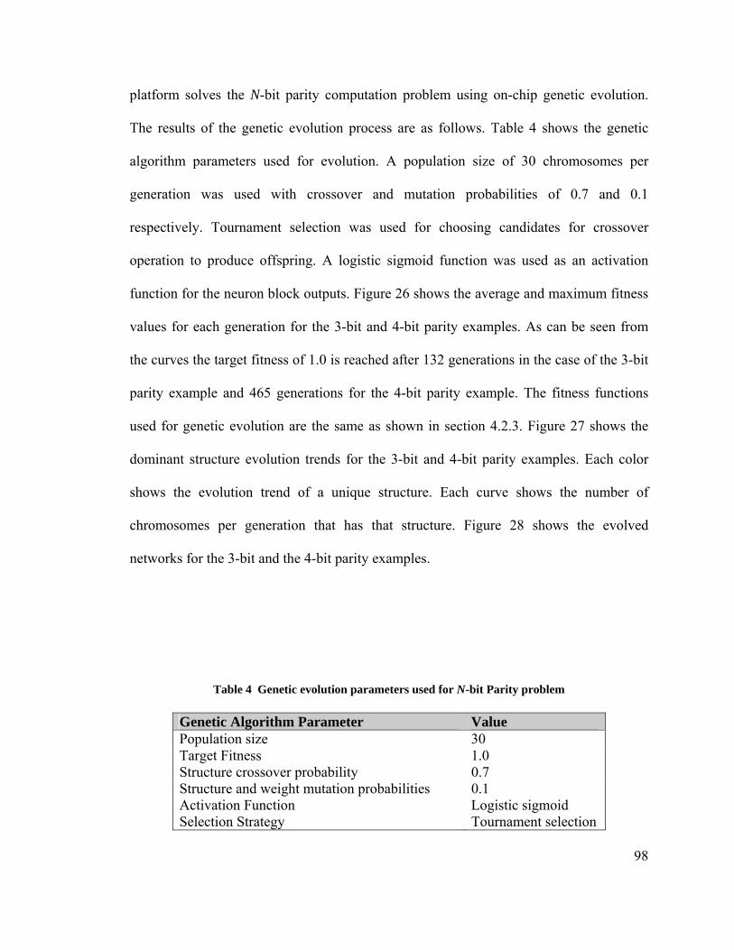
98
platform solves the N-bit parity computation problem using on-chip genetic evolution.
The results of the genetic evolution process are as follows. Table 4 shows the genetic
algorithm parameters used for evolution. A population size of 30 chromosomes per
generation was used with crossover and mutation probabilities of 0.7 and 0.1
respectively. Tournament selection was used for choosing candidates for crossover
operation to produce offspring. A logistic sigmoid function was used as an activation
function for the neuron block outputs. Figure 26 shows the average and maximum fitness
values for each generation for the 3-bit and 4-bit parity examples. As can be seen from
the curves the target fitness of 1.0 is reached after 132 generations in the case of the 3-bit
parity example and 465 generations for the 4-bit parity example. The fitness functions
used for genetic evolution are the same as shown in section 4.2.3. Figure 27 shows the
dominant structure evolution trends for the 3-bit and 4-bit parity examples. Each color
shows the evolution trend of a unique structure. Each curve shows the number of
chromosomes per generation that has that structure. Figure 28 shows the evolved
networks for the 3-bit and the 4-bit parity examples.
Table 4 Genetic evolution parameters used for N-bit Parity problem
Genetic Algorithm Parameter Value Population size 30 Target Fitness 1.0 Structure crossover probability 0.7 Structure and weight mutation probabilities 0.1 Activation Function Logistic sigmoid Selection Strategy Tournament selection
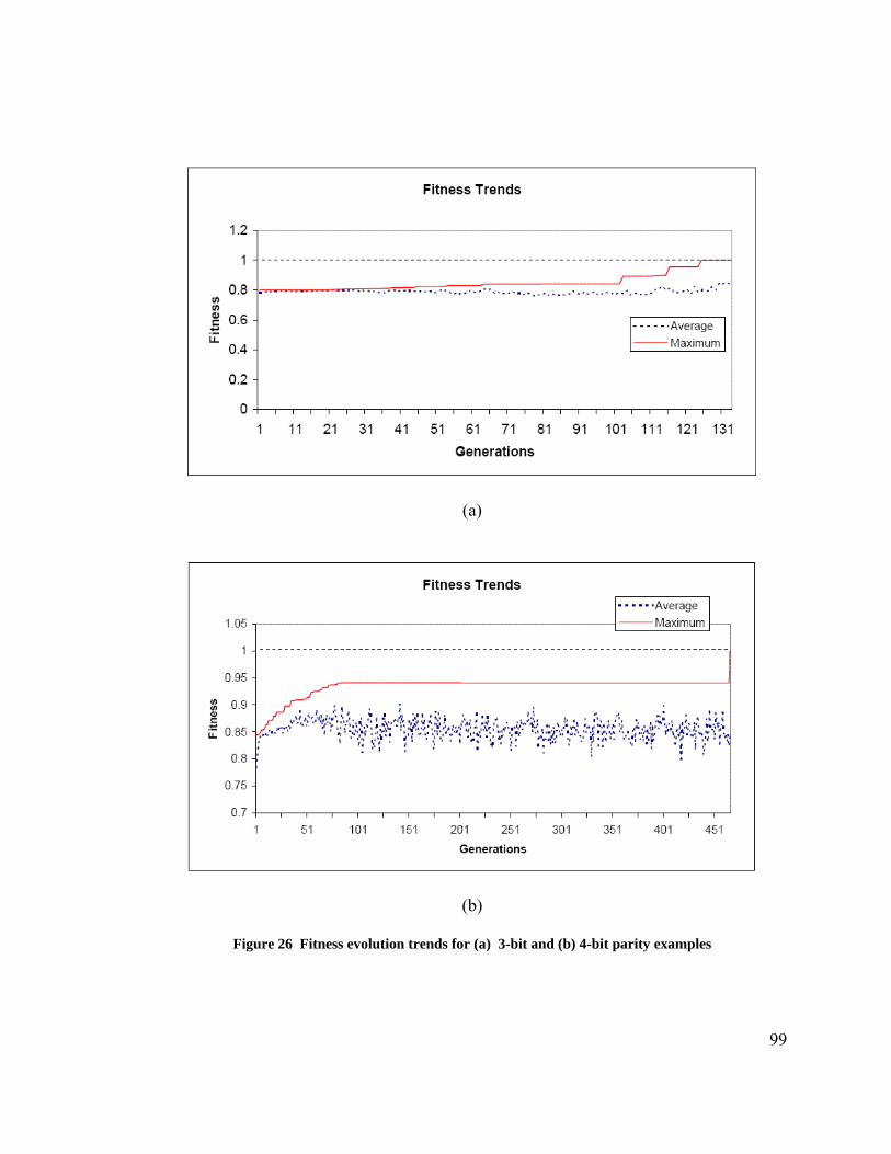
99
(a)
(b)
Figure 26 Fitness evolution trends for (a) 3-bit and (b) 4-bit parity examples
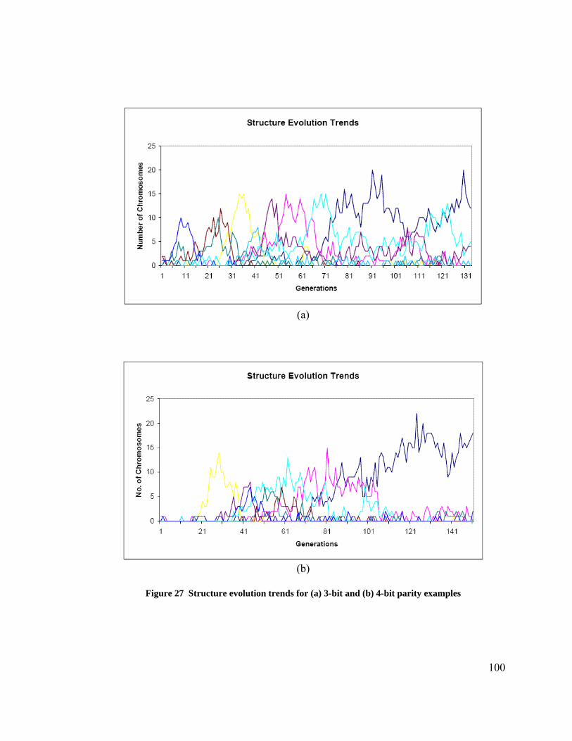
100
(a)
(b)
Figure 27 Structure evolution trends for (a) 3-bit and (b) 4-bit parity examples
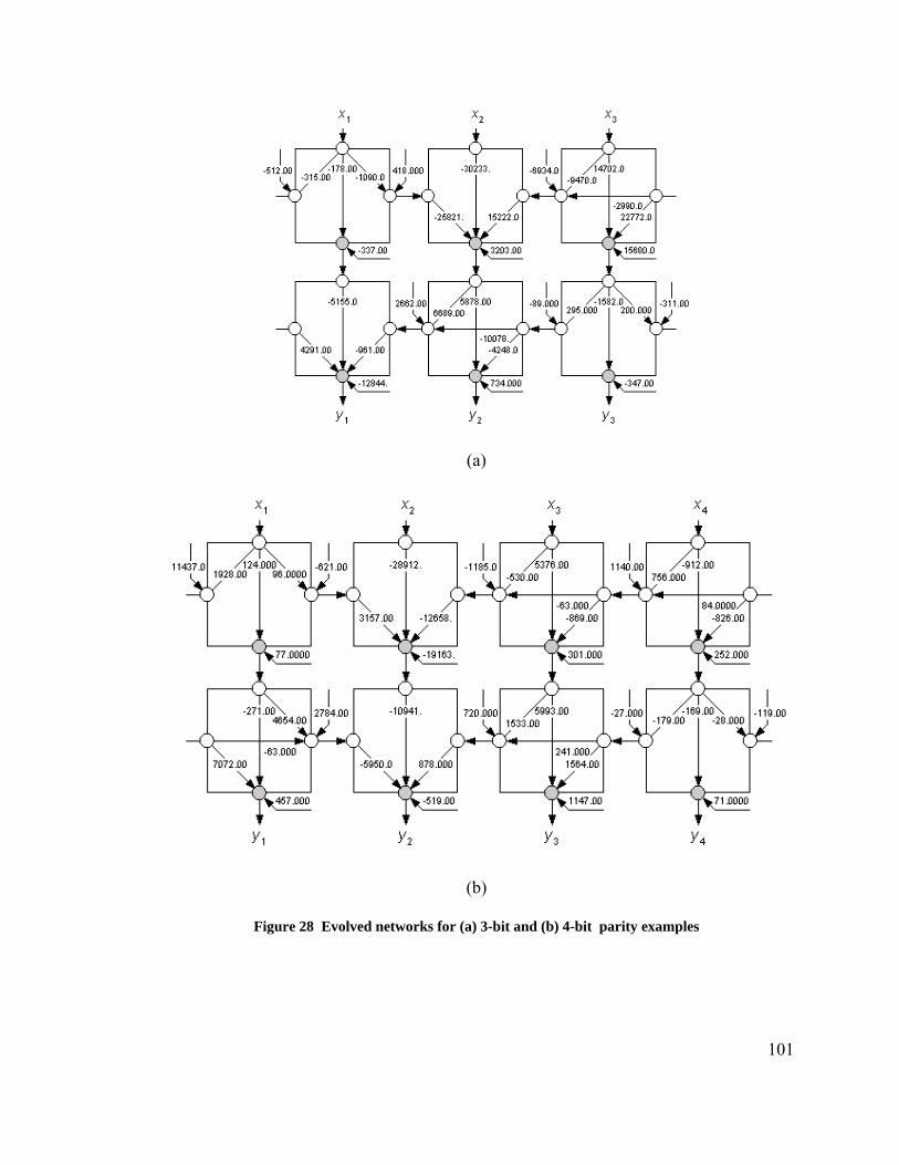
101
(a)
(b)
Figure 28 Evolved networks for (a) 3-bit and (b) 4-bit parity examples

102
The selection, crossover, and mutation genetic operators used to produce new
generations execute on the on-chip PowerPC processor. The execution time to execute
the assembly instructions to produce each generation depends on the population size, the
number of new offspring produced per generation, and the crossover and mutation
probabilities. For the case of the N-bit parity example, the average time it takes to
produce a new generation on the PPC405 processor running at 300MHz is 11 µs. The
population fitness evaluation speed depends on the population size, network structure of
individuals in the population, designated output nodes, and number of input patterns. For
the N-bit parity example, the fitness processing speed ranges from 147 MCPS to 294
MCPS.
5.6.2 Iris Plant Classification
Plant classification is the identification of the plant by observing some unique
attributes such as shape or area of the leaves. Specific shape measurements such as length
and width of the leaves or their area are typically used to automate the classification
using machine learning techniques such as neural networks. The Iris plant classification
problem addressed here is a widely used benchmark for neural classifiers originally
compiled by R.A Fisher [204]. The Iris plant database has data for three classes of Iris
plants, Iris Setosa, Iris Versicolour and Iris Virginica. The dataset has a total of 150
samples, with 50 samples per class instance. The dataset attributes are sepal length, sepal
width, petal length, and petal width for the three classes of the Iris plants. The Iris Setosa
class is linearly separable from the other two classes, Iris Versicolour and Iris Virginica.

103
The latter are not linearly separable from each other. BbNN was used to classify the
plants in this dataset. The results show less than a 1.5% misclassification rate (see Figure
29). For this BbNN genetic evolution, the entire set of 150 samples was used as the
training dataset. The inputs for the network are the sepal area and the petal area
calculated by multiplying the sepal width with the sepal length, and the petal width with
the petal length, respectively. The population size of 80 chromosomes was used for
evolution over 10,000 generations. The structure crossover and mutation probabilities
were set at 0.7 and 0.1, respectively. The weight mutation probability was set at 0.1.
Table 5 shows the various genetic evolution parameters used. Figure 30 shows the
average and maximum fitness trends of the genetic evolution process. Maximum fitness
of 0.99 was achieved after 9403 generations. Figure 31 shows the top few structure
evolution trends. As before, each color is a unique BbNN structure. The values of the
curves indicate the number of chromosomes with the same structure in the particular
generation. Figure 32 shows the evolved network. In the case of the Iris plant
classification example, the average time it takes to produce a new generation on the
PPC405 processor running at 300MHz is 23µs. As discussed above, the population
fitness evaluation speed depends on the population size, network structure of individuals
in the population, designated output nodes, and number of input patterns. The fitness
processing speed for the Iris plant classification example ranges from 147 MCPS to 441
MCPS.
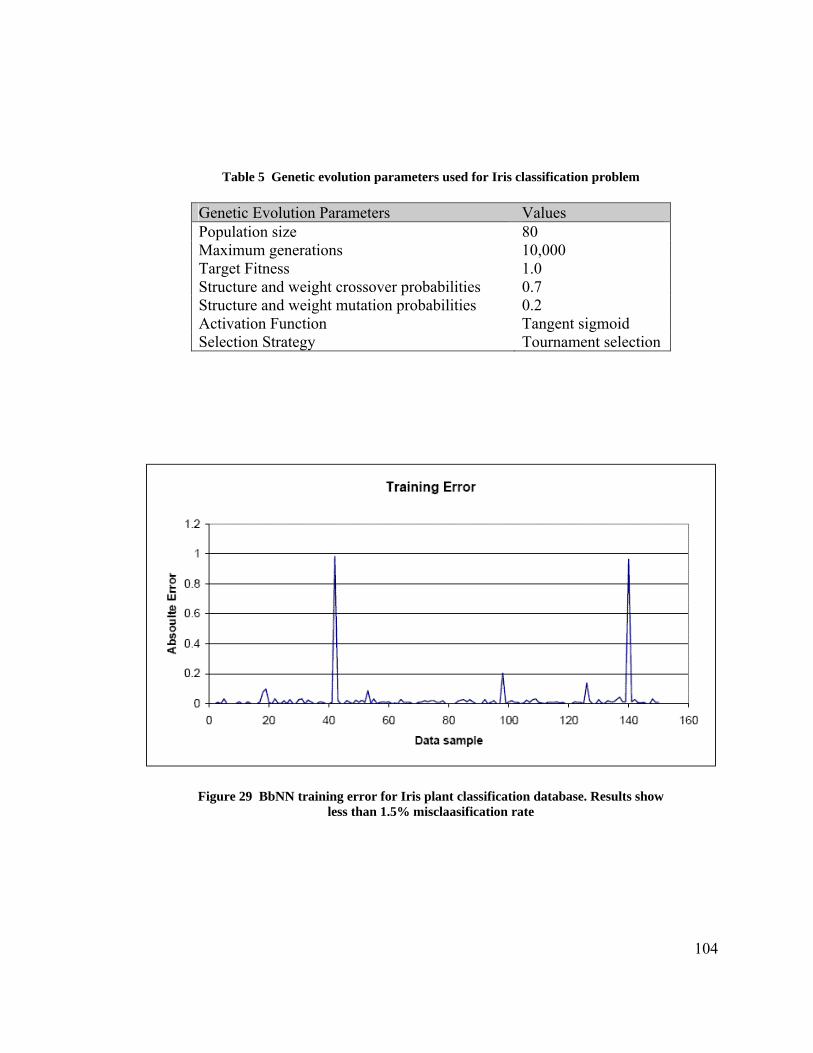
Table 5 Genetic evolution parameters used for Iris classification problem
Genetic Evolution Parameters Values Population size 80 Maximum generations 10,000 Target Fitness 1.0 Structure and weight crossover probabilities 0.7 Structure and weight mutation probabilities 0.2 Activation Function Tangent sigmoid Selection Strategy Tournament selection
Figure 29 BbNN training error for Iris plant classification database. Results show less than 1.5% misclaasification rate
104
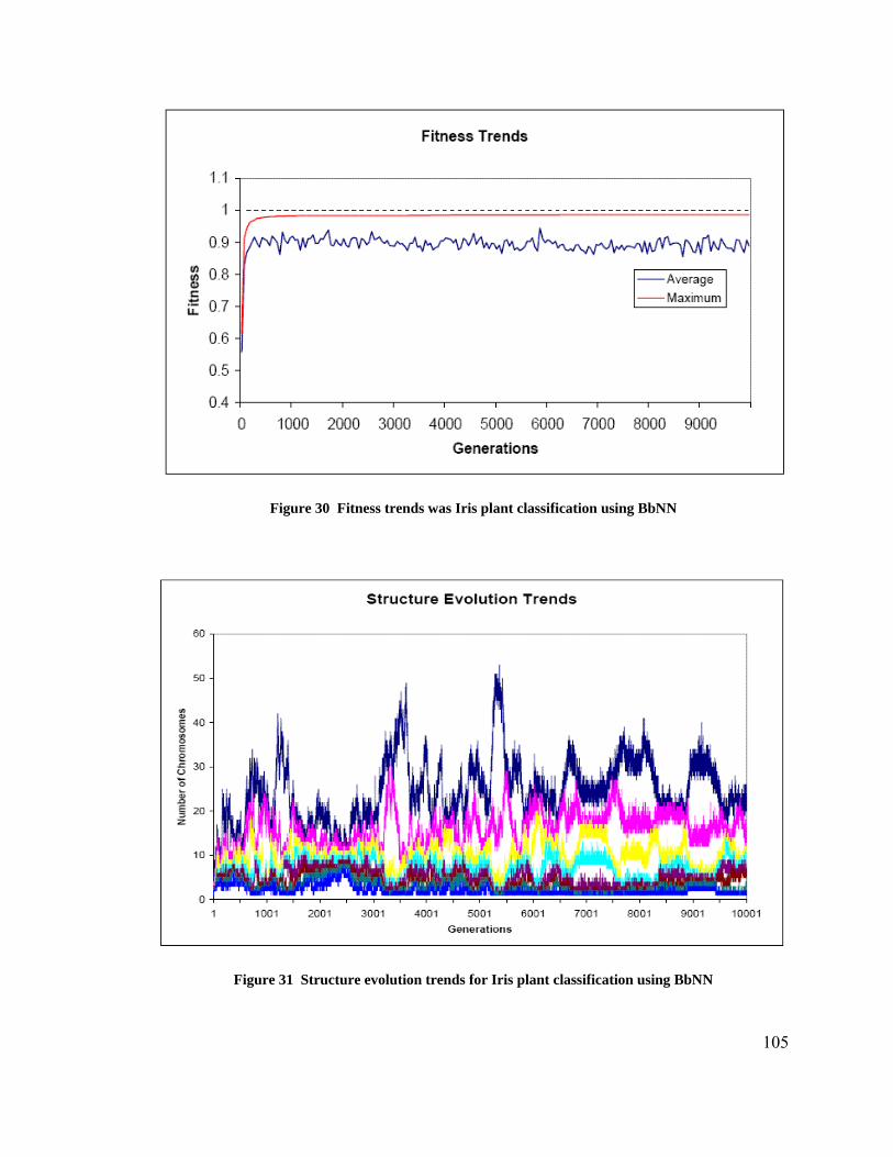
Figure 30 Fitness trends was Iris plant classification using BbNN
Figure 31 Structure evolution trends for Iris plant classification using BbNN
105
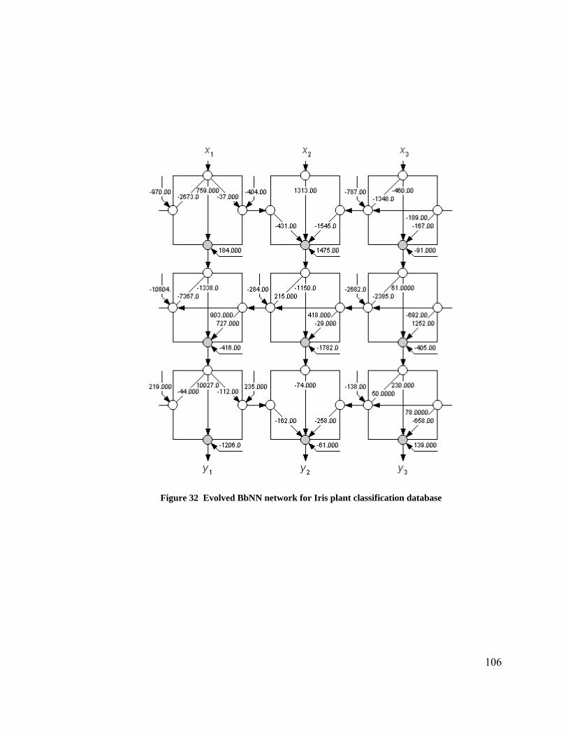
Figure 32 Evolved BbNN network for Iris plant classification database
106
107
5.7 Summary
This chapter presents the FPGA design details of the evolvable BbNN platform.
The design was targeted for a Xilinx Virtex-II Pro FPGA (XC2VP30) housed on a Xilinx
University Program (XUP) FPGA development board or an Amirix AP130 FPGA
development board. The implementation is an intrinsically evolvable, functional-level
EHW platform. The functional units are the neuron blocks of the BbNN.
BbNNs are evolved using genetic algorithms to learn the characteristics of the
training input patterns. The evolution is a multi-parametric optimization problem
requiring simultaneous network structure and synaptic weight optimizations. The network
structure defines the dataflow through the network from the inputs to the outputs and the
internal configurations of the neuron blocks. Each neuron block can have one of the four
possible internal configurations depending on the positions of the inputs and the outputs.
The SBbN implementation presented dynamically adapts to different internal neuron
block configurations based on the network structure specified in the BbNN chromosome.
The synaptic weights and biases have been implemented as registers and can be updated
dynamically. Thus, the implementation of the BbNNs presented here can be evolved
intrinsically on the FPGA and does not require any runtime FPGA reconfiguration cycles.
This saves the overheads of FPGA reconfiguration times that are typically in millisecond
range (see section 2.5.2.2). The dataflow between the neuron blocks is handled
asynchronously using a P/T dataflow network model. This enables larger networks to be
scaled across multiple FPGAs and evolve in parallel or to use the same FPGA network in
108
a time-multiplexed manner for larger networks that cannot be accommodated on a single
FPGA. The genetic algorithm used to evolve the BbNNs runs on the on-chip PowerPC
processor in the Virtex-II Pro FPGA. The population fitness evaluations are performed
directly on the BbNN hardware. Thus, the system can be deployed as a compact,
embedded, evolvable platform in real-world applications.
Chapter 6 introduces the online learning with the BbNNs and presents an
application that demonstrates the intrinsic online evolution capability of the design.
6 ONLINE LEARNING WITH BBNNS
BbNNs can be used for applications of artificial neural networks such as pattern
classification, signal prediction, function approximation, process control and feature
recognition. In the past, BbNNs have been applied to mobile robot navigation [23],
multivariate gaussian distributed pattern classification [182], chaotic time series
prediction [183], ECG signal classification and heart beat monitoring [4, 5], and Iris plant
classification [186]. The on-chip training capability of the developed BbNN platform
extends its capabilities to a number of different applications in dynamic environments.
A recurring concern of using artificial neural networks in practical applications is
its ability to generalize and apply its training knowledge satisfactorily. A training dataset
that is a good representative set of the actual data that the network may be exposed to in
practice is important for good generalization. But this is difficult to achieve, especially in
dynamic or unpredictable environments requiring retraining of structure and parameters
of the network. Under such circumstances the ability of online training is important to
maintain reliable system performance. The on-chip training capability of the developed
BbNN platform is ideally suited for applications in dynamic environments. This chapter
presents an online training approach for BbNN platform and an application to
demonstrate its capabilities.
109
110
6.1 Online Training Approach
With the advantage of on-chip training capability, the developed BbNN platform
can be deployed in dynamic environments and programmed to adapt to variances in
environmental stimuli. The network can be deployed in an actor-critic fashion with the
network in the active mode performing the actor’s role and a critic analyzing the
responses of the network to the environmental stimuli. There are three online evolvable
system deployment scenarios envisioned.
1. The deployed network is in active mode producing the outputs to input stimuli
from the environment. The critic constantly analyzes the network’s performance
and on recognizing deviations beyond a certain threshold either in the expected
network outputs, the inputs, or performance, can trigger a network retraining
cycle to adapt to the variances in the environment. In this scenario the network is
switched between the training and the active modes as dictated by the critic.
2. In the second scenario, the network can be scheduled to automatically switch
between the training and the active modes in a time-multiplexed approach. The
critic, on detecting deviations in performance beyond the threshold, can deploy
the last known fittest network obtained in the training mode to the active mode to
improve the system performance. This is illustrated in Figure 33.
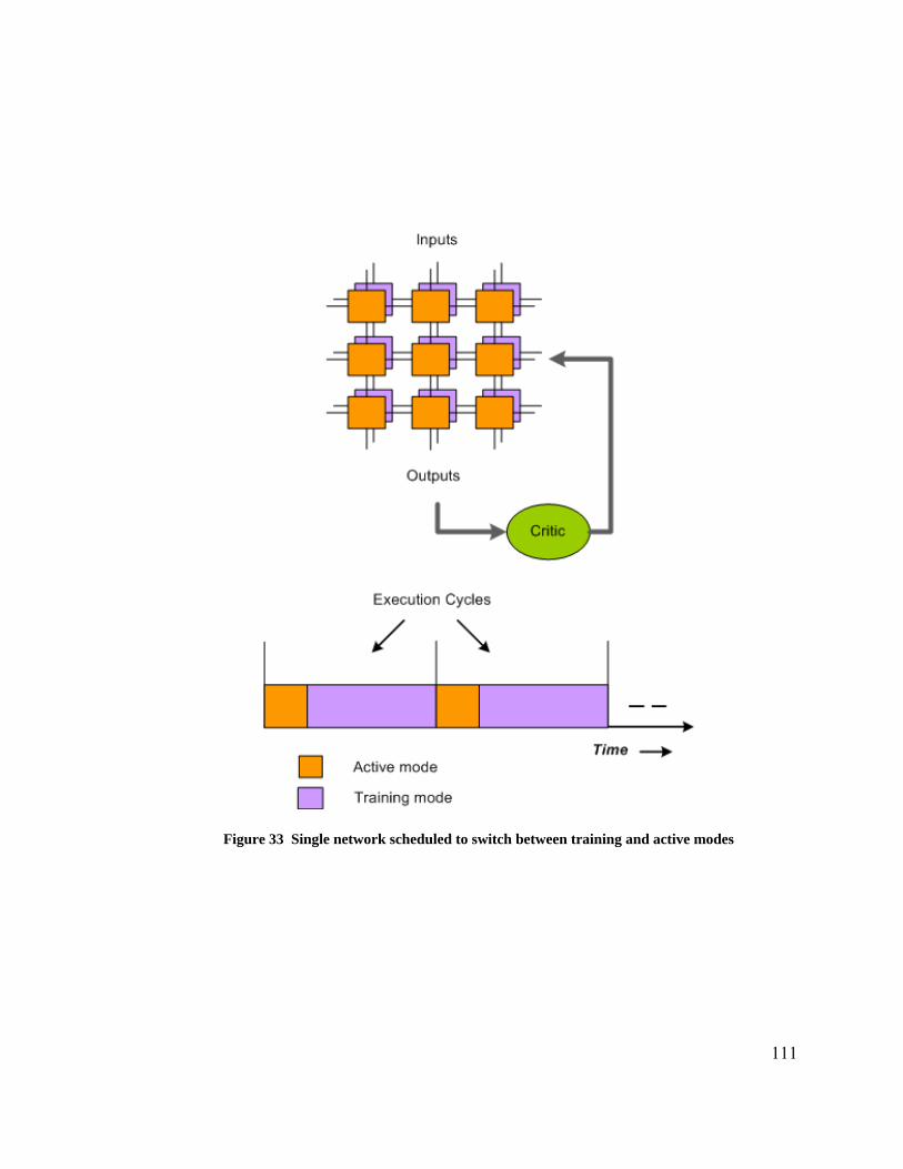
Figure 33 Single network scheduled to switch between training and active modes
111
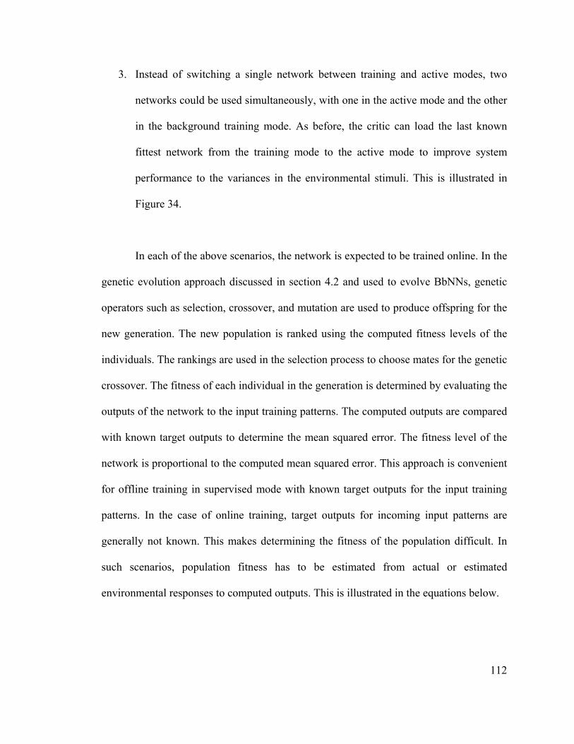
112
3. Instead of switching a single network between training and active modes, two
networks could be used simultaneously, with one in the active mode and the other
in the background training mode. As before, the critic can load the last known
fittest network from the training mode to the active mode to improve system
performance to the variances in the environmental stimuli. This is illustrated in
Figure 34.
In each of the above scenarios, the network is expected to be trained online. In the
genetic evolution approach discussed in section 4.2 and used to evolve BbNNs, genetic
operators such as selection, crossover, and mutation are used to produce offspring for the
new generation. The new population is ranked using the computed fitness levels of the
individuals. The rankings are used in the selection process to choose mates for the genetic
crossover. The fitness of each individual in the generation is determined by evaluating the
outputs of the network to the input training patterns. The computed outputs are compared
with known target outputs to determine the mean squared error. The fitness level of the
network is proportional to the computed mean squared error. This approach is convenient
for offline training in supervised mode with known target outputs for the input training
patterns. In the case of online training, target outputs for incoming input patterns are
generally not known. This makes determining the fitness of the population difficult. In
such scenarios, population fitness has to be estimated from actual or estimated
environmental responses to computed outputs. This is illustrated in the equations below.
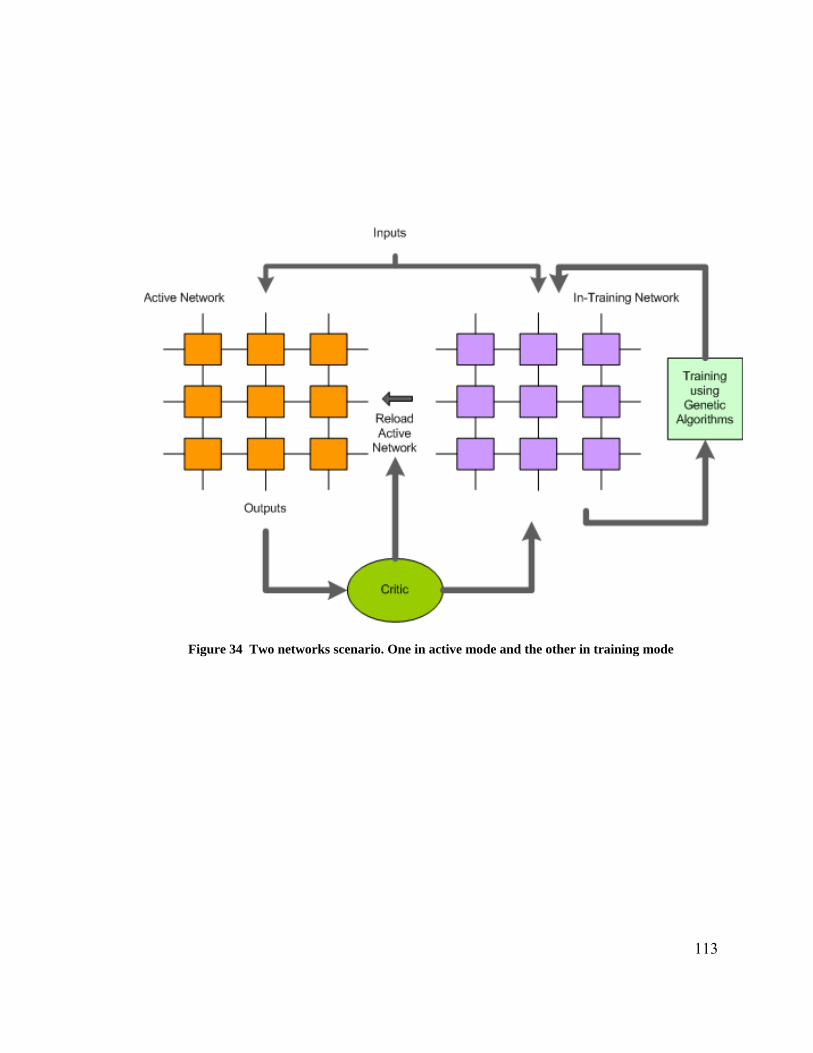
113
Figure 34 Two networks scenario. One in active mode and the other in training mode

Network output is a function of the inputs, the current environmental state, and
the network structure and parameters. Thus, if the inputs are , the current
environmental state is , and represents the network parameters, then the network
output is a function of these variables as shown below.
tX
tS nK
( )nttt KSXfY ,,= (7)
The new state of the environment is a function of the previous state and
the outputs as shown below.
1+tS tS
tY
( )ttt SYfS ,1 =+ (8)
The estimated fitness is the function of the new state and the desired state
of the environment.
1+tS
∧+1tS
⎟⎟⎠
⎞⎜⎜⎝
⎛=
∧++ 11, ttn SSfF (9)
If the fitness can be estimated with reasonable confidence level, the genetic
algorithm approach used in the offline supervised evolution can be used for online
evolution.
114
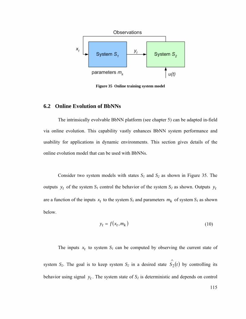
Figure 35 Online training system model
6.2 Online Evolution of BbNNs
The intrinsically evolvable BbNN platform (see chapter 5) can be adapted in-field
via online evolution. This capability vastly enhances BbNN system performance and
usability for applications in dynamic environments. This section gives details of the
online evolution model that can be used with BbNNs.
Consider two system models with states S1 and S2 as shown in Figure 35. The
outputs of the system S1 control the behavior of the system S2 as shown. Outputs
are a function of the inputs to the system S1 and parameters of system S1 as shown
below.
ty ty
tx km
( )ktt mxfy ,= (10)
The inputs to system S1 can be computed by observing the current state of
system S2. The goal is to keep system S2 in a desired state by controlling its
behavior using signal . The system state of S2 is deterministic and depends on control
tx
( )tS∧2
ty
115

input and the current value of an input time-varying signal to system S2.
signal behavior depends on external factors that may not be controllable by our system
models. To maintain system S2 in the desired state at all times, it is essential to predict the
future behavior of signal in advance to adjust S1 model parameters that control
the S2 system inputs .
ty )(tu )(tu
)(tu km
ty
We can use online evolution with the BbNNs to predict the future values of the
signal from its current and past values. The current value of the signal can be
determined as shown below.
)(tu )(tu
The expected system state at time t, is a function of control inputs to the
system S2 as shown below.
( )tS−2 ty
( ) ( )tyftS =−2 (11)
The current value of can be computed from the observed state )(tu ( )tS2 , the
expected state , and the predicted . ( )tS−2 ( )tu
−
( ) ( ) ( ) ( )⎟⎟⎠
⎞⎜⎜⎝
⎛=
−−tutStSftu ,, 22 (12)
116
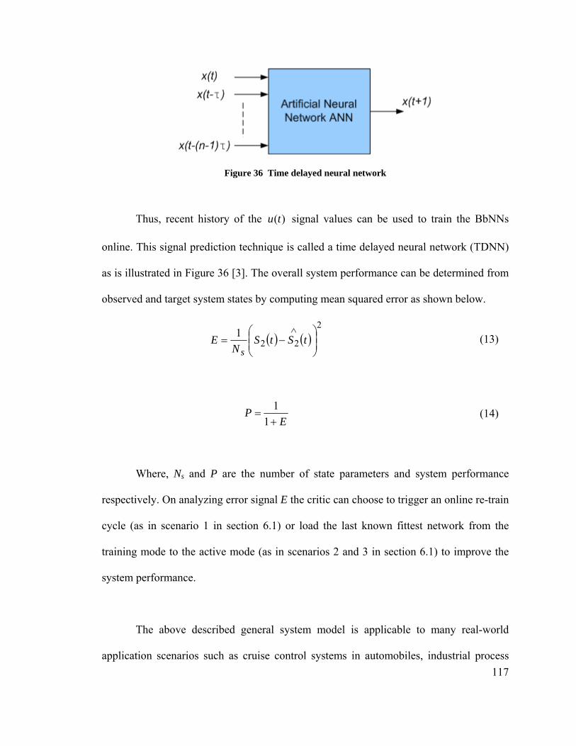
Figure 36 Time delayed neural network
117
Thus, recent history of the signal values can be used to train the BbNNs
online. This signal prediction technique is called a time delayed neural network (TDNN)
as is illustrated in Figure 36 [3]. The overall system performance can be determined from
observed and target system states by computing mean squared error as shown below.
)(tu
( ) ( )2
221
⎟⎟⎠
⎞⎜⎜⎝
⎛−=
∧tStS
NE
s (13)
EP
+=
11 (14)
Where, Ns and P are the number of state parameters and system performance
respectively. On analyzing error signal E the critic can choose to trigger an online re-train
cycle (as in scenario 1 in section 6.1) or load the last known fittest network from the
training mode to the active mode (as in scenarios 2 and 3 in section 6.1) to improve the
system performance.
The above described general system model is applicable to many real-world
application scenarios such as cruise control systems in automobiles, industrial process

118
control, prediction of solar radiation dosage levels, or guidance systems in aircraft. The
following section demonstrates online evolution of BbNNs using an example application.
6.3 Case Study: Adaptive Neural Luminosity Controller
An important issue facing this generation is the global climate change due to the
effects of greenhouse gas emissions and increased energy consumption. Conservation of
energy is of prime importance to check the greenhouse gas emissions and conserve
depleting resources. According to the Clinton Climate Initiative (CCI) program of former
US president William J. Clinton, 75% of the global emissions of greenhouse gases come
from the cities and 50% of the city’s emissions are generated by its buildings. The CCI
program is fervently promoting a Global Energy Efficiency Building Retrofit Program to
reduce energy consumption in a city’s buildings [205]. The benefits of energy
conservation in buildings not only helps fight global climate change but also results in
considerable savings in energy costs. This application is motivated by the needs of energy
conservation and reducing the energy costs.
A huge portion of the energy consumption in a building is the lighting. Most
people prefer illuminated corridors and well lit rooms and hallways in the buildings. Our
aim is to control the lumen outputs of the lamps in the buildings to maintain a sufficient
illumination as per requirements at different times of the day. The amount of illumination
in a room varies depending on the ambient light intensity, which is dependent on factors
such as time of day, windows, shades and curtains, and object shadows. These factors are

time and space variant and hence the amount of illumination in a room varies with the
ambient light intensity levels. To provide the target illumination levels we need to
intelligently control the lumen outputs of the lamps illuminating a room depending on the
ambient light intensity levels.
This application fits the system model described in section 6.2. Signal
corresponds to the control inputs to the electronic ballasts used to regulate the light
intensity outputs of the lamps. Signal can be obtained by observing the current light
intensity levels, i.e. the outputs of the light sensors in the room. The time varying signal
is the ambient light intensity and the desired target state is the target light
intensity level. If the ambient light intensity levels can be predicted we can control the
luminosity levels in the room by adjusting the control inputs to the electronic ballasts. To
predict the ambient luminosity levels in the room we used online evolution with BbNNs.
ty
tx
( )tu∧2S
The following discussion lays out the simulation experimental setup and the
approach.
119

120
6.3.1 Simulation Experimental Setup
Figure 37 shows a layout (top view and front view) of a room with area 30’×10’
used as the reference room for our simulation experiment. The room has 7 fluorescent
light fixtures and 2 light sensors attached to the ceiling as shown. The reference
illumination surface is an oblong conference table shown in the figure. The distances
between light and sensor placements as well as the reference surface are as shown in
Figure 37. The room has a large window (not shown in the front view) on the wall
opposite to that of the door. Each light fixture has associated electronic ballast used to
control lumen output of the lights. The ballasts are assumed to be similar to Lutron Eco-
10TM TVETM, fluorescent dimming ballast from Lutron Electronics Co [206]. The ballasts
support continuous, flicker-free dimming from 100% to 10% of measured relative light
output with control inputs ranging from 0-10VDC. Further, the ballasts have a linear
dimming curve with respect to control input voltage as shown in Figure 38 [206]. For the
sake of our simulation we will assume that all the fluorescent lamps are identical in terms
of their lumen outputs and corresponding power consumption. The contribution to the
light intensity levels on the reference surface by the lamps will be governed by the
inverse square law. This means, if a lamp lumen output is L foot-candles (FC) then the
light intensity at a point at a distance d from the lamp source will be L / d2. The light
sensors used are linear photodiode sensors similar to commercial sensors available from
PLC Multipoint Inc. [207]. These are low voltage light sensors with linear voltage signal
characteristics with respect to the measured light intensity. The plot in Figure 39
illustrates the linear output characteristics of the photodiode sensors.
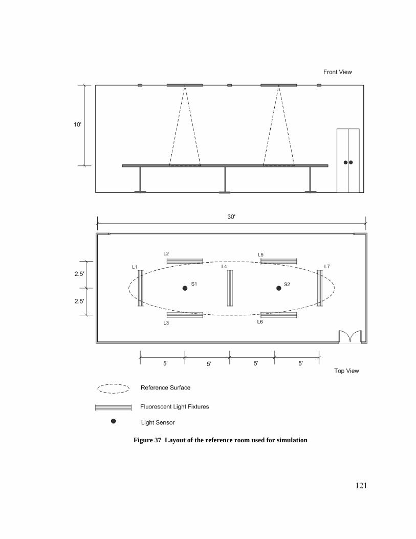
Figure 37 Layout of the reference room used for simulation
121
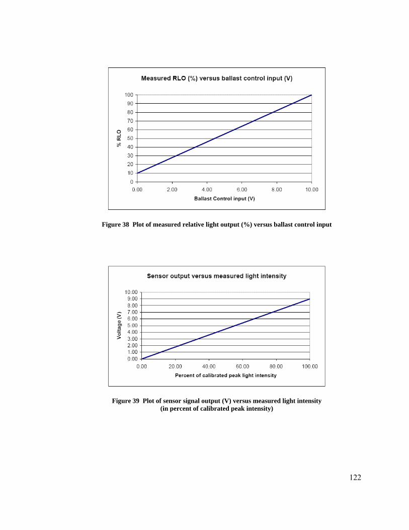
Figure 38 Plot of measured relative light output (%) versus ballast control input
Figure 39 Plot of sensor signal output (V) versus measured light intensity (in percent of calibrated peak intensity)
122
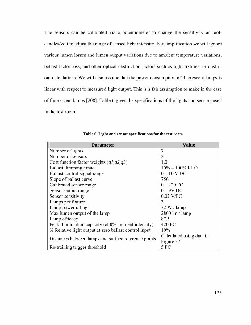
123
The sensors can be calibrated via a potentiometer to change the sensitivity or foot-
candles/volt to adjust the range of sensed light intensity. For simplification we will ignore
various lumen losses and lumen output variations due to ambient temperature variations,
ballast factor loss, and other optical obstruction factors such as light fixtures, or dust in
our calculations. We will also assume that the power consumption of fluorescent lamps is
linear with respect to measured light output. This is a fair assumption to make in the case
of fluorescent lamps [208]. Table 6 gives the specifications of the lights and sensors used
in the test room.
Table 6 Light and sensor specifications for the test room
Parameter Value Number of lights 7 Number of sensors 2 Cost function factor weights (q1,q2,q3) 1.0 Ballast dimming range 10% – 100% RLO Ballast control signal range 0 – 10 V DC Slope of ballast curve 756 Calibrated sensor range 0 – 420 FC Sensor output range 0 – 9V DC Sensor sensitivity 0.02 V/FC Lamps per fixture 3 Lamp power rating 32 W / lamp Max lumen output of the lamp 2800 lm / lamp Lamp efficacy 87.5 Peak illumination capacity (at 0% ambient intensity) 420 FC % Relative light output at zero ballast control input 10%
Distances between lamps and surface reference points Calculated using data in Figure 37
Re-training trigger threshold 5 FC

6.3.2 Adaptive BbNN Predictor
As discussed in section 6.2, we will use collected history of the ambient light
intensity levels during the course of the day to train the BbNNs using genetic algorithms
for predicting the future ambient light intensity levels. Ambient light intensity level at the
current time step ‘t’ can be estimated from the current luminosity readings of the
reference surface by the light sensors and the expected light intensity levels at the
reference surface due to the lamp outputs. For our simulation example we will assume the
identical ambient light intensity levels throughout the entire reference surface.
∑−==
N
i i
iSA
d
LLL
j 1 2 (15)
where,
jSL Light intensity at reference surface of sensor Sj
Li Lumen output of light fixture i N Total number of light fixtures di Distance in feet between the light fixture i and reference surface LA Ambient light intensity at reference surface
For our simulation purposes we will assume the ideal ambient light intensity
varies at different times of day (time step = 10 mins) as shown in Figure 40. The
luminosity levels in the plot are % of the peak light intensity at the reference surface
provided by all the light fixtures running at full capacity and 0 foot-candle ambient light
levels. This is about 420 foot-candles for our test room as calculated from maximum
lamp lumen outputs and the distances between reference surface and the lamps. This
124
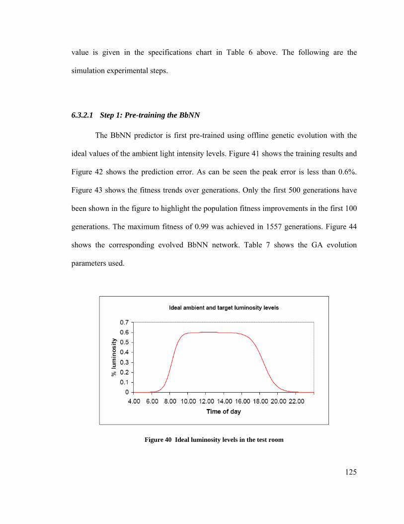
value is given in the specifications chart in Table 6 above. The following are the
simulation experimental steps.
6.3.2.1 Step 1: Pre-training the BbNN
The BbNN predictor is first pre-trained using offline genetic evolution with the
ideal values of the ambient light intensity levels. Figure 41 shows the training results and
Figure 42 shows the prediction error. As can be seen the peak error is less than 0.6%.
Figure 43 shows the fitness trends over generations. Only the first 500 generations have
been shown in the figure to highlight the population fitness improvements in the first 100
generations. The maximum fitness of 0.99 was achieved in 1557 generations. Figure 44
shows the corresponding evolved BbNN network. Table 7 shows the GA evolution
parameters used.
Figure 40 Ideal luminosity levels in the test room
125
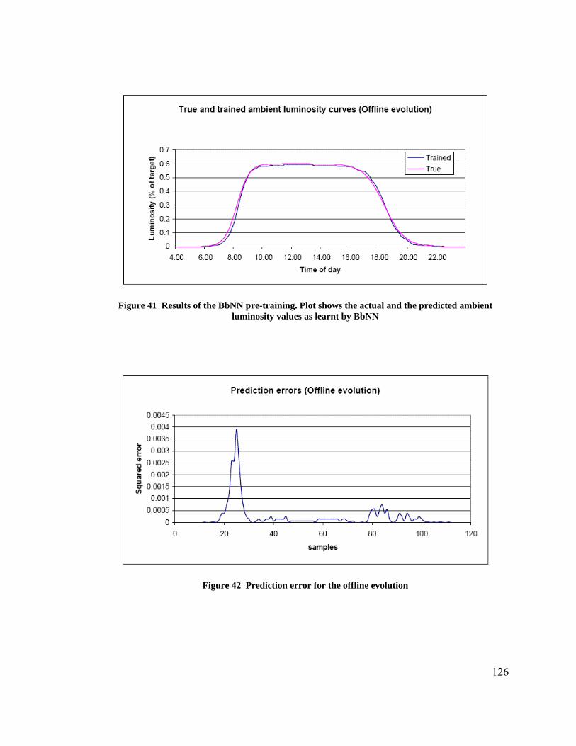
Figure 41 Results of the BbNN pre-training. Plot shows the actual and the predicted ambient luminosity values as learnt by BbNN
Figure 42 Prediction error for the offline evolution
126
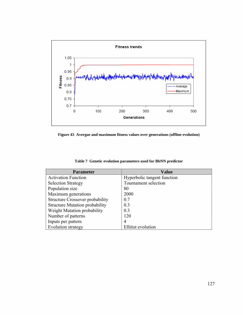
Figure 43 Avergae and maximum fitness values over generations (offline evolution)
Table 7 Genetic evolution parameters used for BbNN predictor
Parameter Value Activation Function Hyperbolic tangent function Selection Strategy Tournament selection Population size 80 Maximum generations 2000 Structure Crossover probability 0.7 Structure Mutation probability 0.3 Weight Mutation probability 0.3 Number of patterns 120 Inputs per pattern 4 Evolution strategy Ellitist evolution
127
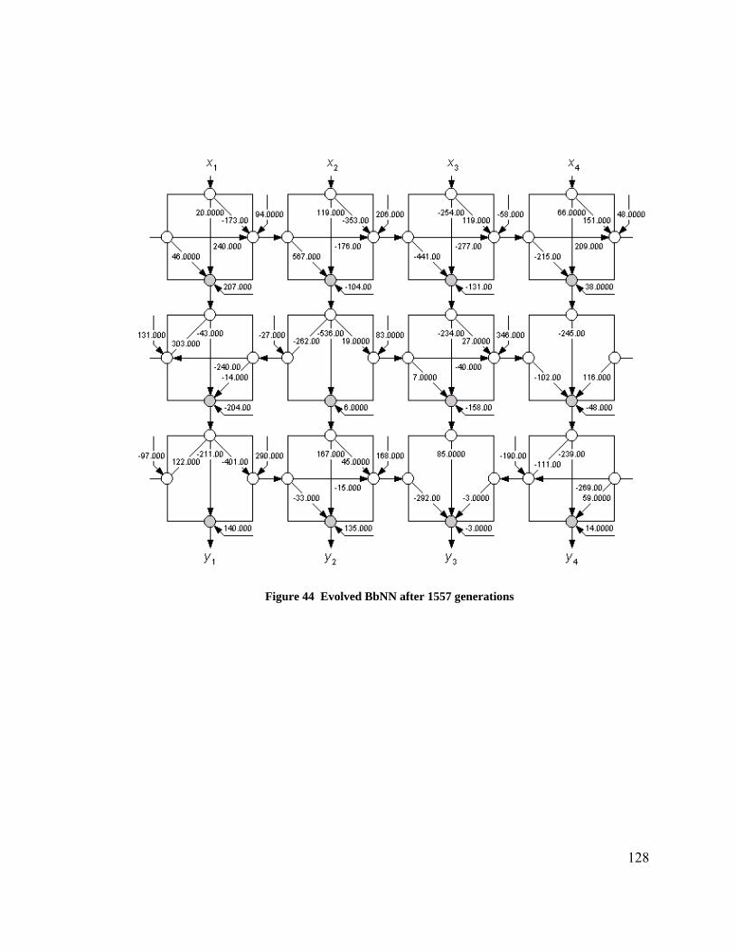
Figure 44 Evolved BbNN after 1557 generations
128
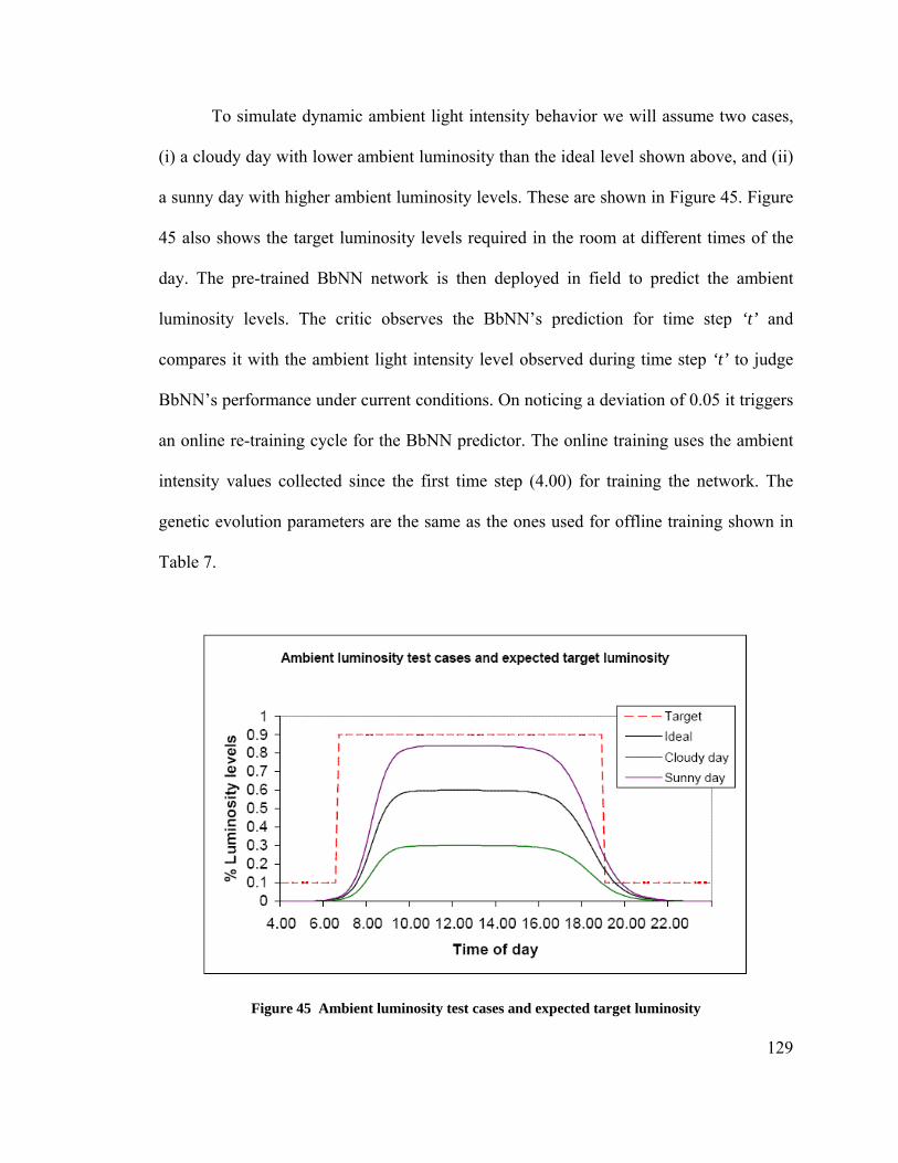
To simulate dynamic ambient light intensity behavior we will assume two cases,
(i) a cloudy day with lower ambient luminosity than the ideal level shown above, and (ii)
a sunny day with higher ambient luminosity levels. These are shown in Figure 45. Figure
45 also shows the target luminosity levels required in the room at different times of the
day. The pre-trained BbNN network is then deployed in field to predict the ambient
luminosity levels. The critic observes the BbNN’s prediction for time step ‘t’ and
compares it with the ambient light intensity level observed during time step ‘t’ to judge
BbNN’s performance under current conditions. On noticing a deviation of 0.05 it triggers
an online re-training cycle for the BbNN predictor. The online training uses the ambient
intensity values collected since the first time step (4.00) for training the network. The
genetic evolution parameters are the same as the ones used for offline training shown in
Table 7.
Figure 45 Ambient luminosity test cases and expected target luminosity
129
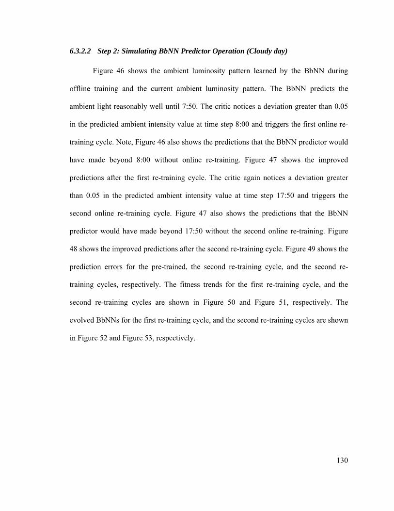
130
6.3.2.2 Step 2: Simulating BbNN Predictor Operation (Cloudy day)
Figure 46 shows the ambient luminosity pattern learned by the BbNN during
offline training and the current ambient luminosity pattern. The BbNN predicts the
ambient light reasonably well until 7:50. The critic notices a deviation greater than 0.05
in the predicted ambient intensity value at time step 8:00 and triggers the first online re-
training cycle. Note, Figure 46 also shows the predictions that the BbNN predictor would
have made beyond 8:00 without online re-training. Figure 47 shows the improved
predictions after the first re-training cycle. The critic again notices a deviation greater
than 0.05 in the predicted ambient intensity value at time step 17:50 and triggers the
second online re-training cycle. Figure 47 also shows the predictions that the BbNN
predictor would have made beyond 17:50 without the second online re-training. Figure
48 shows the improved predictions after the second re-training cycle. Figure 49 shows the
prediction errors for the pre-trained, the second re-training cycle, and the second re-
training cycles, respectively. The fitness trends for the first re-training cycle, and the
second re-training cycles are shown in Figure 50 and Figure 51, respectively. The
evolved BbNNs for the first re-training cycle, and the second re-training cycles are shown
in Figure 52 and Figure 53, respectively.
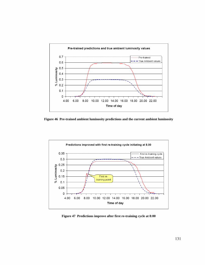
Figure 46 Pre-trained ambient luminosity predictions and the current ambient luminosity
Figure 47 Predictions improve after first re-training cycle at 8:00
131
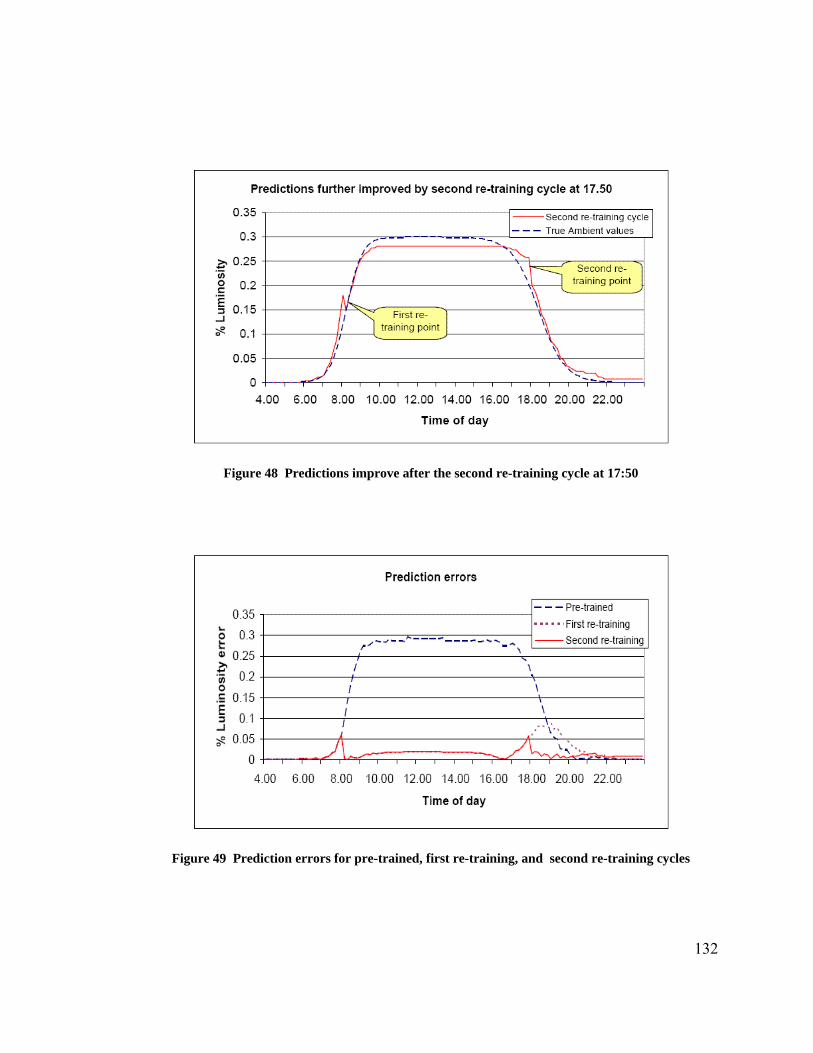
Figure 48 Predictions improve after the second re-training cycle at 17:50
Figure 49 Prediction errors for pre-trained, first re-training, and second re-training cycles
132
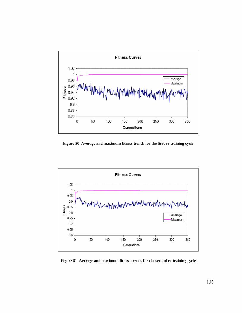
Figure 50 Average and maximum fitness trends for the first re-training cycle
Figure 51 Average and maximum fitness trends for the second re-training cycle
133
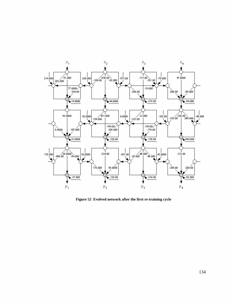
Figure 52 Evolved network after the first re-training cycle
134
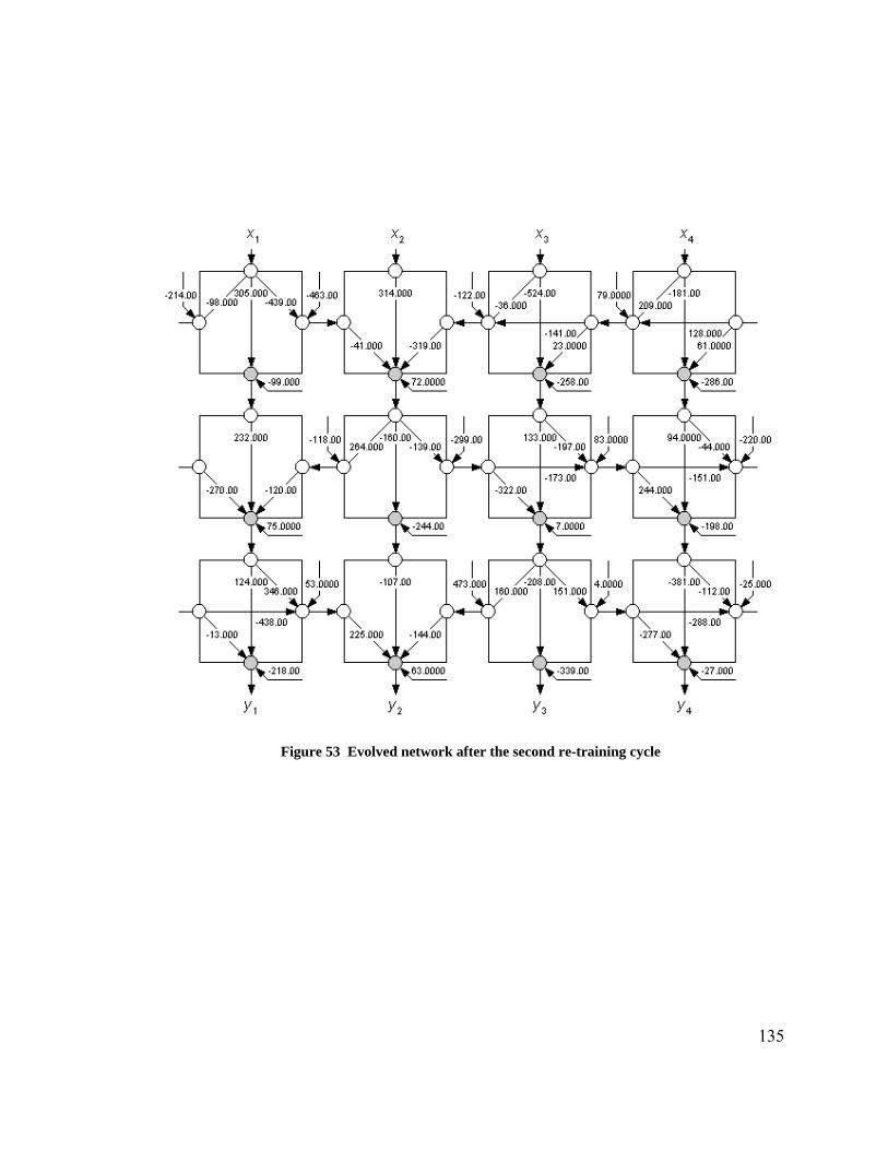
Figure 53 Evolved network after the second re-training cycle
135

6.3.2.3 Step 3: Simulating the BbNN Controller Operation (Cloudy day)
In Step 2, evolution was used to predict the ambient light intensity values. To
control and maintain the luminosity levels in the test room we need to adjust the ballast
control inputs. There are 7 light fixtures in the room with one ballast per fixture. Hence
we have 7 ballast control inputs to adjust. Our goal is to maintain the target illumination
levels and minimize the energy consumption of the lights. Another goal is to maintain all
the lights at about the same intensity levels to increase the relative lifetime of all the
lamps. So our cost function for this minimization problem should account for each of
these factors. It can be modeled as shown below.
( ) ( ) ( )xUqxGqxPqCFFunctionCost 321 ++= (16)
where,
321 ,, qandqq Weights for each of the factors in the cost function ( )xP Estimated average power consumption per lamp ( )xG Estimated average deviation from the target luminosity
level per sensor ( )xU Factor for load distribution across the lamps
x BbNN controller outputs
Average power consumption per lamp can be calculated from the ballast control
inputs (BbNN outputs) and the reported lamp efficacy by the lamp manufacturer as
shown in the equations below.
( ) ( )∑==
N
iixP
NxP
1
1 (17)
136
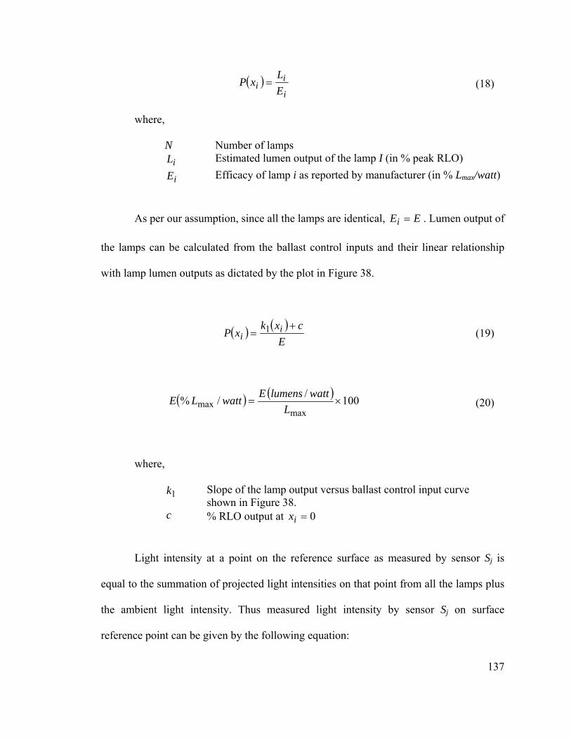
( )i
ii E
LxP = (18)
where,
N Number of lamps iL Estimated lumen output of the lamp I (in % peak RLO)
iE Efficacy of lamp i as reported by manufacturer (in % Lmax/watt)
As per our assumption, since all the lamps are identical, . Lumen output of
the lamps can be calculated from the ballast control inputs and their linear relationship
with lamp lumen outputs as dictated by the plot in Figure 38.
EEi =
( ) ( )E
cxkxP i
i+
= 1 (19)
( ) ( ) 100//%max
max ×=L
wattlumensEwattLE (20)
where,
1k Slope of the lamp output versus ballast control input curve shown in Figure 38.
c % RLO output at 0=ix
Light intensity at a point on the reference surface as measured by sensor Sj is
equal to the summation of projected light intensities on that point from all the lamps plus
the ambient light intensity. Thus measured light intensity by sensor Sj on surface
reference point can be given by the following equation:
137
AN
i i
iS L
d
LL
j+∑=
=1 2 (21)
AN
i i
iS L
d
cxkL
j+∑
+=
=1 21 (22)
The estimated average deviation G(x) from the target luminosity level LT as
measured by M sensors is thus given as shown in the following equation:
( ) ( )⎟⎟⎠
⎞⎜⎜⎝
⎛∑ −==
M
jTS LLabs
MxG
j1
1 (23)
To ensure equivalent load distribution across all the lamps we can include a load
factor U(x) in the cost function as shown below.
( ) ( )ki xxxU −= max (24)
This is a linear problem and can be solved easily solved by a BbNN of grid size 1
x 7. Each of the 7 outputs of the BbNN can be used to control the electronic ballasts. We
will refer to this BbNN as the BbNN controller in the discussion below to avoid
confusion with the BbNN predictor, described above, used to predict the ambient light
intensity values. At every time-step the BbNN predictor described above can feed the
predicted ambient light intensity values to the BbNN controller. The controller can
evolve to find optimal values for the ballast control inputs. We can use the equation
below as a fitness function for GA evolution.
138

CFCFFFitness −= max (25)
Table 8 shows the genetic evolution parameters used by the BbNN controller.
Figure 54 shows the complete BbNN predictor - controller system used in this case study.
Figure 55 shows the target and actual luminosity levels (in FC) in the room with pre-
trained ambient prediction values. Figure 56 shows the corresponding luminosity error.
The large deviation from target luminosity observed is due to poor ambient luminosity
predictions in the pre-trained case. Using the online evolution vastly improves the
luminosity levels in the room with little deviations from target values. This can be seen in
Figure 57 which shows the target and actual luminosity levels in the room with ambient
prediction values obtained with online evolution. Figure 58 shows the corresponding
luminosity error. The spike observed in the luminosity error between 19:00 and 20:00 is
due to the high ambient luminosity then required. The ballast control inputs during these
times are at 0V, which corresponds to 10% relative light output of the lamps. This is the
minimal setting for the ballasts used. So the spike observed in the luminosity error curve
is actually due to the summation of 10% lamp output and the ambient light intensity.
Figure 59 shows the power consumption (in watts) by the lights for the case of pre-
trained BbNN predictor. Figure 60 shows the power consumption values with using
online evolvable BbNN predictor. We can see that the average power consumption
increases for the case of online evolvable BbNN predictor as compared to the pre-trained
results. This is because the luminosity levels for the pre-trained case are significantly
lower than the required target luminosity. The lights are dimmer as the ambient intensity
predictions are much higher than the actual in the pre-trained case.
139
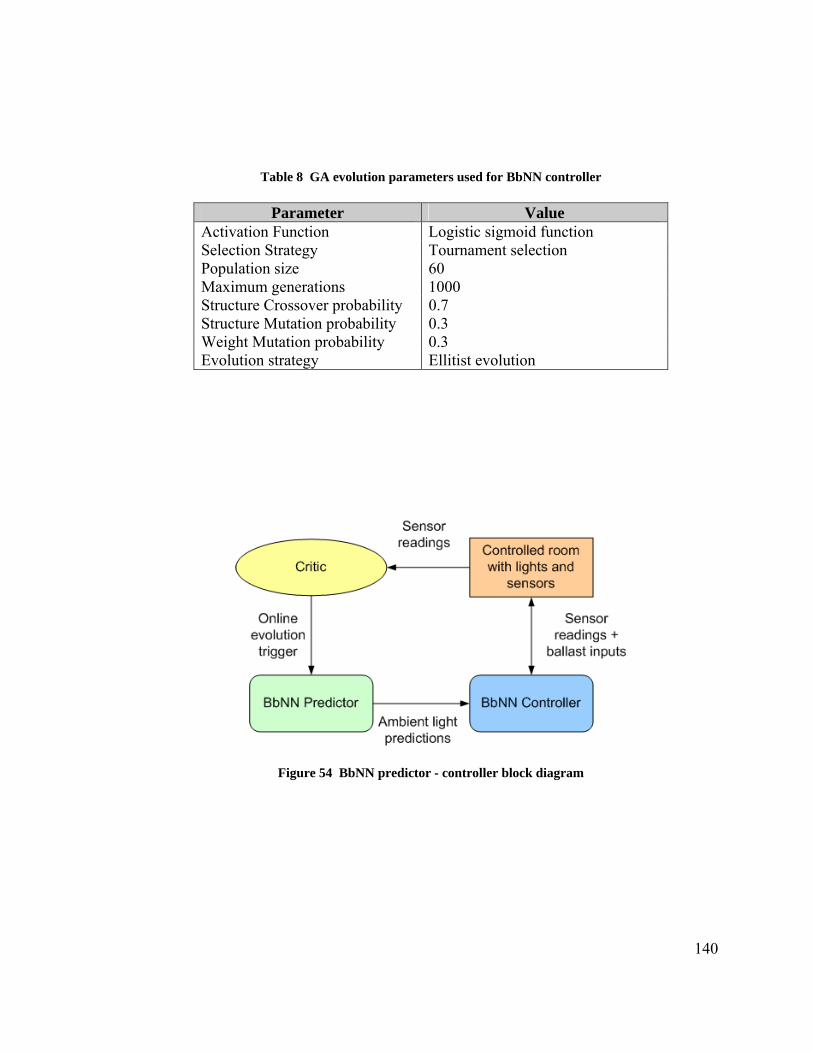
Table 8 GA evolution parameters used for BbNN controller
Parameter Value Activation Function Logistic sigmoid function Selection Strategy Tournament selection Population size 60 Maximum generations 1000 Structure Crossover probability 0.7 Structure Mutation probability 0.3 Weight Mutation probability 0.3 Evolution strategy Ellitist evolution
Figure 54 BbNN predictor - controller block diagram
140
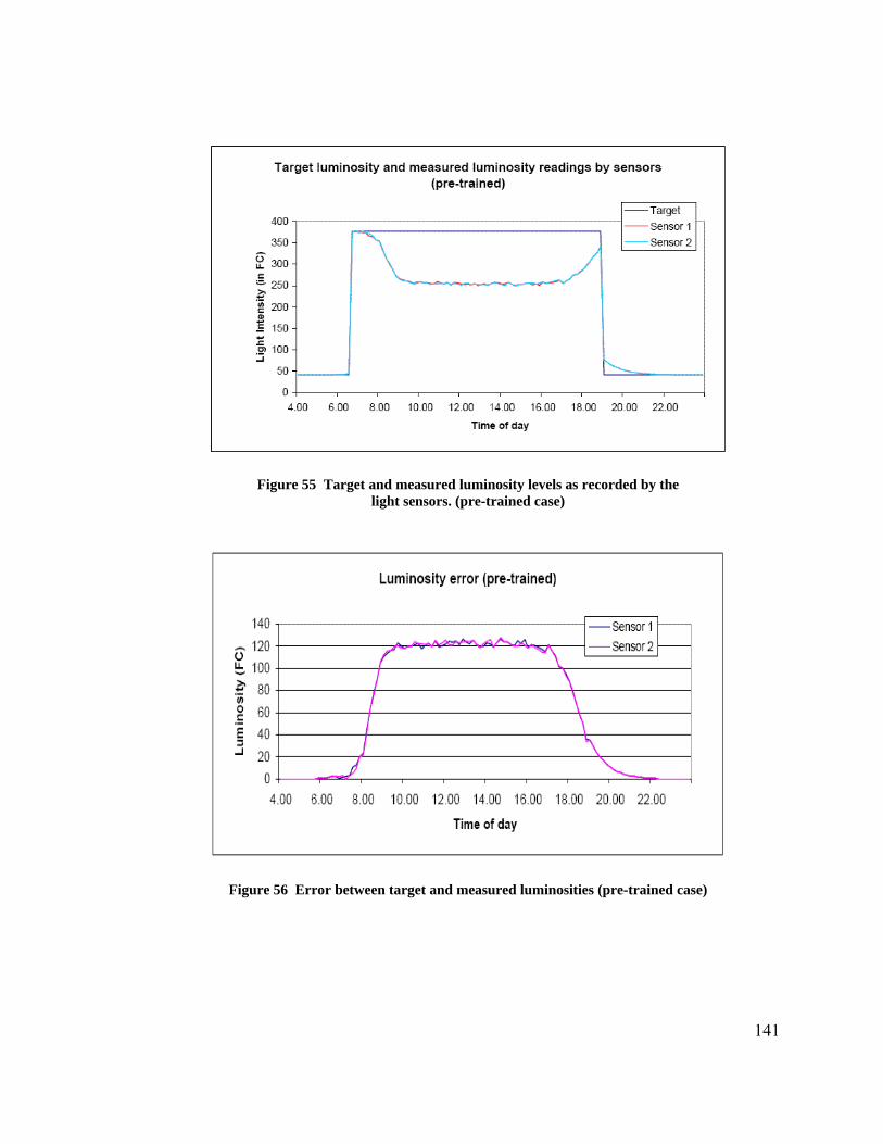
Figure 55 Target and measured luminosity levels as recorded by the light sensors. (pre-trained case)
Figure 56 Error between target and measured luminosities (pre-trained case)
141
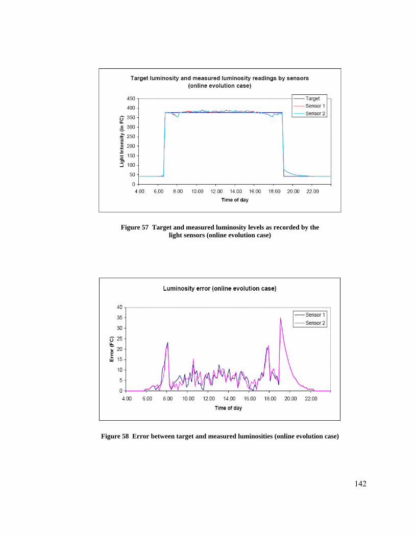
Figure 57 Target and measured luminosity levels as recorded by the light sensors (online evolution case)
Figure 58 Error between target and measured luminosities (online evolution case)
142
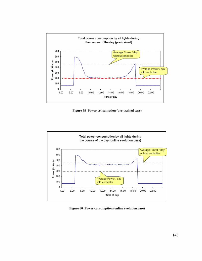
Figure 59 Power consumption (pre-trained case)
Figure 60 Power consumption (online evolution case)
143

144
The plots also show the average power consumption for the case of not using any
predictors or controllers and simply turning the lights ‘ON’ at full capacity when the
target intensity levels are 0.9. Using the BbNN predictor-controller saved an average of
140W throughout the day. At an average daily rate of $0.15 per KWhr, this resulted in
savings of $0.42 in energy costs per room per day. For a large skyscraper the savings
quickly add up. Figure 61 shows the fitness curves and evolved network of the BbNN
controller for the 4:00 time step as an example of the BbNN controller module.
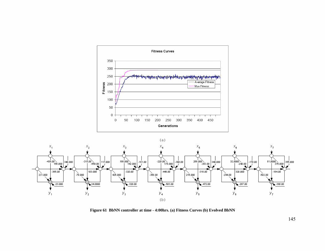
145
(a)
(b)
Figure 61 BbNN controller at time - 4:00hrs. (a) Fitness Curves (b) Evolved BbNN
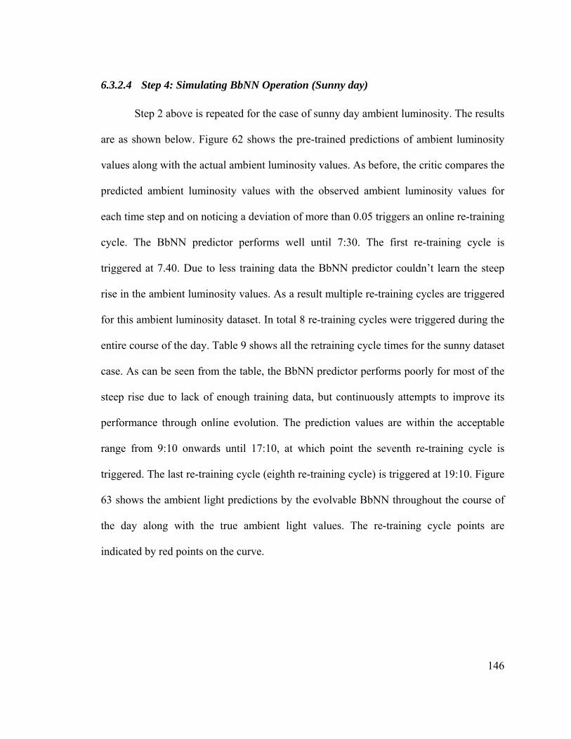
146
6.3.2.4 Step 4: Simulating BbNN Operation (Sunny day)
Step 2 above is repeated for the case of sunny day ambient luminosity. The results
are as shown below. Figure 62 shows the pre-trained predictions of ambient luminosity
values along with the actual ambient luminosity values. As before, the critic compares the
predicted ambient luminosity values with the observed ambient luminosity values for
each time step and on noticing a deviation of more than 0.05 triggers an online re-training
cycle. The BbNN predictor performs well until 7:30. The first re-training cycle is
triggered at 7.40. Due to less training data the BbNN predictor couldn’t learn the steep
rise in the ambient luminosity values. As a result multiple re-training cycles are triggered
for this ambient luminosity dataset. In total 8 re-training cycles were triggered during the
entire course of the day. Table 9 shows all the retraining cycle times for the sunny dataset
case. As can be seen from the table, the BbNN predictor performs poorly for most of the
steep rise due to lack of enough training data, but continuously attempts to improve its
performance through online evolution. The prediction values are within the acceptable
range from 9:10 onwards until 17:10, at which point the seventh re-training cycle is
triggered. The last re-training cycle (eighth re-training cycle) is triggered at 19:10. Figure
63 shows the ambient light predictions by the evolvable BbNN throughout the course of
the day along with the true ambient light values. The re-training cycle points are
indicated by red points on the curve.
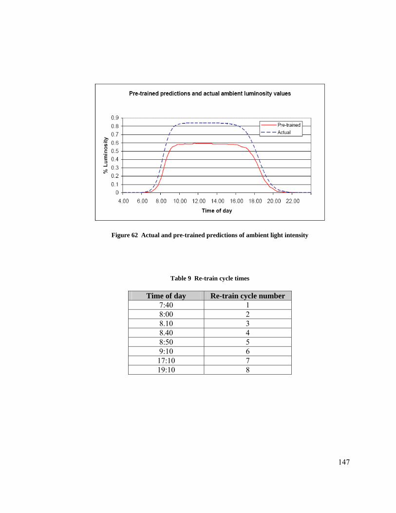
Figure 62 Actual and pre-trained predictions of ambient light intensity
Table 9 Re-train cycle times
Time of day Re-train cycle number 7:40 1 8:00 2 8.10 3 8.40 4 8:50 5 9:10 6 17:10 7 19:10 8
147
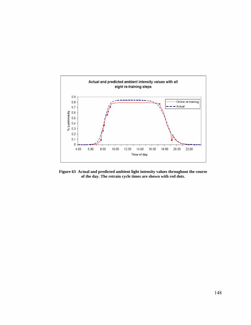
Figure 63 Actual and predicted ambient light intensity values throughout the course of the day. The retrain cycle times are shown with red dots.
148
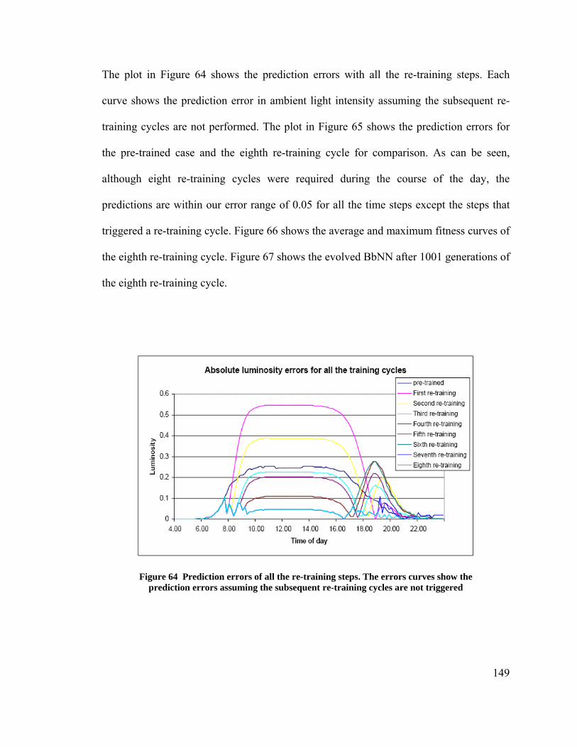
The plot in Figure 64 shows the prediction errors with all the re-training steps. Each
curve shows the prediction error in ambient light intensity assuming the subsequent re-
training cycles are not performed. The plot in Figure 65 shows the prediction errors for
the pre-trained case and the eighth re-training cycle for comparison. As can be seen,
although eight re-training cycles were required during the course of the day, the
predictions are within our error range of 0.05 for all the time steps except the steps that
triggered a re-training cycle. Figure 66 shows the average and maximum fitness curves of
the eighth re-training cycle. Figure 67 shows the evolved BbNN after 1001 generations of
the eighth re-training cycle.
Figure 64 Prediction errors of all the re-training steps. The errors curves show the prediction errors assuming the subsequent re-training cycles are not triggered
149
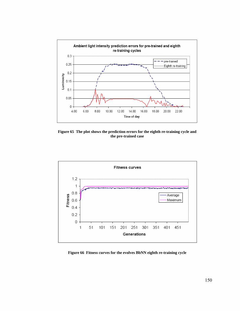
Figure 65 The plot shows the prediction errors for the eighth re-training cycle and the pre-trained case
Figure 66 Fitness curves for the evolves BbNN eighth re-training cycle
150
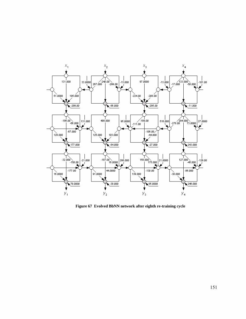
Figure 67 Evolved BbNN network after eighth re-training cycle
151
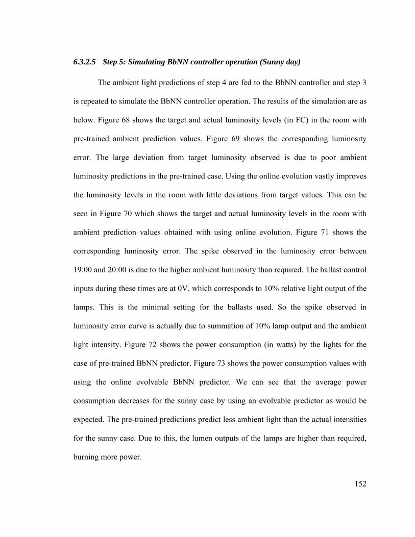
152
6.3.2.5 Step 5: Simulating BbNN controller operation (Sunny day)
The ambient light predictions of step 4 are fed to the BbNN controller and step 3
is repeated to simulate the BbNN controller operation. The results of the simulation are as
below. Figure 68 shows the target and actual luminosity levels (in FC) in the room with
pre-trained ambient prediction values. Figure 69 shows the corresponding luminosity
error. The large deviation from target luminosity observed is due to poor ambient
luminosity predictions in the pre-trained case. Using the online evolution vastly improves
the luminosity levels in the room with little deviations from target values. This can be
seen in Figure 70 which shows the target and actual luminosity levels in the room with
ambient prediction values obtained with using online evolution. Figure 71 shows the
corresponding luminosity error. The spike observed in the luminosity error between
19:00 and 20:00 is due to the higher ambient luminosity than required. The ballast control
inputs during these times are at 0V, which corresponds to 10% relative light output of the
lamps. This is the minimal setting for the ballasts used. So the spike observed in
luminosity error curve is actually due to summation of 10% lamp output and the ambient
light intensity. Figure 72 shows the power consumption (in watts) by the lights for the
case of pre-trained BbNN predictor. Figure 73 shows the power consumption values with
using the online evolvable BbNN predictor. We can see that the average power
consumption decreases for the sunny case by using an evolvable predictor as would be
expected. The pre-trained predictions predict less ambient light than the actual intensities
for the sunny case. Due to this, the lumen outputs of the lamps are higher than required,
burning more power.
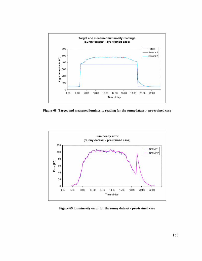
Figure 68 Target and measured luminosity reading for the sunnydataset - pre-trained case
Figure 69 Luminosity error for the sunny dataset - pre-trained case
153
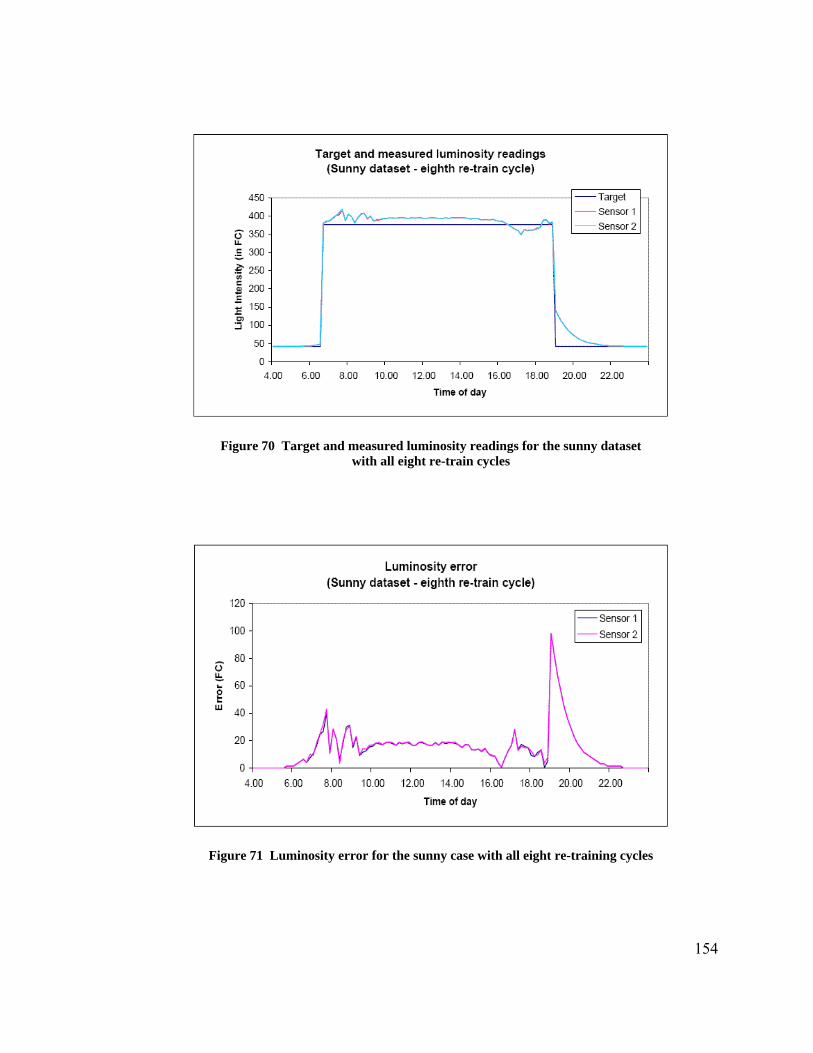
Figure 70 Target and measured luminosity readings for the sunny dataset with all eight re-train cycles
Figure 71 Luminosity error for the sunny case with all eight re-training cycles
154
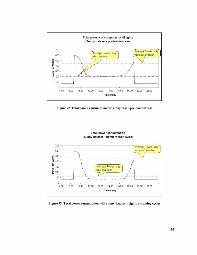
Figure 72 Total power consumption for sunny case - pre-trained case
Figure 73 Total power consumption with sunny dataset - eight re-training cycles
155
156
The plots also show the average power consumption for the case of not using any
predictors or controllers and simply turning the lights ‘ON’ at full capacity for target
intensity levels of 0.9. Using the BbNN predictor-controller to regulate the luminosity in
the room saved on an average 310W throughout the day. At an average daily rate of
$0.15 per KWhr, this resulted in savings of $0.93 in energy costs per room per day.
6.4 Summary
This chapter presented the concepts of online evolution with the BbNNs and
demonstrated simulation of a case study using the evolvable BbNN platform in a
dynamic environment. A training dataset that is a good representation of the actual data
processed by the artificial neural networks is difficult to obtain in practice. This is
especially true for applications of artificial neural networks in dynamic environments.
The capability of online adaptation in a dynamically changing environment significantly
improves system reliability and performance as was seen in the case study. For online
evolution the hardware implementing the artificial neural networks should support
intrinsic training, as in the implementation demonstrated in chapter 5. Online training
capability can also be used to provide a degree of fault tolerance to external component
failures. For example, in response to the failure of one of the input sensors to the network
in-field, the network can be re-trained to ignore the corresponding input and ‘bypass’ the
failure. This ensures reliable operation of rest of the system, or at least provides graceful
degradation in system performance.
7 PERFORMANCE ANALYSIS
This chapter presents a performance model characterizing BbNN implementations
on devices across the computing space. In particular, we compare the computational
throughput of BbNNs across general purpose processors and FPGAs. We explore
performance metrics for quantitative comparison. The chapter is organized as follows.
The concepts for characterizing the computing device space are introduced first followed
by the discussion of performance metrics. Peak throughput of BBNN implementations
across different computing devices is compared and model sensitivity analysis is
presented. The chapter concludes with the analysis of smart block-based neuron models
described in section 5.1.3.
7.1 Computational Device Space
A computational device is a machine that processes data. The technology used to
build this computational machine may vary significantly and can be electronic,
mechanical, bio-computing, or any other technology that can be used to implement
computations. Each set of computational instructions that process data is an individual
functional configuration. The ability of the computational device to support diverse
functional configurations defines its functional diversity. The Computational Device
(CD) space is a broad spectrum of these computational machines and includes different
computational technologies such as VLSI computing, bio-computing, and nano-
157
158
computing. Advances and innovations in these technologies continuously reshape and
broaden this space. The VLSI Processing (VP) space is the part of the CD space occupied
by the VLSI computing devices. This encompasses the computational devices using
semiconductor fabrication processes. The VP space can be characterized by the device
support for functional configuration diversity. At one end of the space are soft computing
devices (also called general purpose computing devices) that can support any functional
configuration depending on the sequence of programmable computing instructions
executed. The hardware circuitry implementing the instructions is programmed on silicon
at the time of fabrication. The instructions facilitate the functional configuration diversity
after fabrication. At the other end of this space are hard computing devices with fixed
functional configurations programmed in hardware at the time of fabrication. These
devices have restrictive functional diversity. The Reconfigurable Processing (RP) space
is a subset of VP space and represents the reconfigurable computing devices. Devices in
the RP space enable diversity in functional configurations using reprogrammable
hardware instructions. These hardware instructions are at lower levels of abstraction than
to the functional configuration sequences in soft computing devices. The hardware
instructions remap/reconfigure the programmable hardware units and their
interconnections.
In this manuscript, the use of the term ‘computational device’ refers to the devices
in the VP space. Although this is a restrictive meaning of the term with reference to our
discussion above, it is convenient to use for the discussion in the rest of this chapter.
159
The broad range of implementation options in the VP space presents many
different choices to pick to implement computations. A particular implementation choice
is based on the examination of various application and resource specific constraints
enforced by the chosen implementation medium. Metrics such as speedup, throughput,
area, power, cost, or some combination of these guide the implementation choice.
Application-specific constraints tend to be unique to a particular application or a set of
applications; hence they are difficult to reasonably generalize. Resource constraints on
the other hand are enforced by the implementation medium and may or may not be
application-specific. Never the less, resource constraints can play an important role in
design decisions for a particular application. For example, an I/O data rate for a particular
implementation medium may be limited by the interconnect bus speeds. Lower bus
speeds may limit the achievable I/O throughput, making the device unsuitable for an I/O-
intensive application such as a network router. In another case, throughput might be
limited by the input data processing speeds achievable with an implementation on a
particular medium. A computationally intensive application may not be served well by
this computing device. To be able to make such informed design decisions, it is
imperative to characterize computing devices with respect to various computational
metrics of interest.
7.2 RP Space
Continued innovations in RP space in the last two decades have blurred the
traditional boundaries between soft and hard computing devices. Devices in this space
160
are broadly categorized as field programmable logic devices (FPLDs). These offer the
flexibility of post-fabrication functional configuration diversity of soft computing devices
along with the custom/semi-custom design advantages of hard computing devices. The
technology offers both coarse-grained as well as fine-grained logic devices. Coarse-
grained logic devices such as the field programmable object array (FPOA) from MathStar
can reprogram functional object behaviors and their interconnections using different
functional configuration instruction streams [209]. Typical functional objects are ALUs,
MACs, and the register files (RFs). Fine-grained logic devices reconfigure gate level
logic circuitry using configuration bitstreams as opposed to reprogramming circuitry at
the functional objects level. Current state of the art of this technology is the field
programmable gate array (FPGA). These devices contain arrays of configurable logic
blocks (also called logic array blocks) interconnected via a configurable interconnection
network. Each logic block is a 4-bit/6-bit LUT plus a flip-flop and can be configured to
emulate a 4-input/6-input logic function or a flip-flop [210]. Configuration instruction
bitstreams reconfigure these logic blocks and their interconnection network providing
post-fabrication functional diversity at logic circuit level. Capacities of these devices
have grown from a few thousand logic blocks per chip just over a decade ago to the order
of a few hundred thousand logic blocks per chip. The regular layout architecture of these
devices on silicon makes them ideally suited to embrace newer fabrication processes with
smaller feature sizes relatively faster as compared to their custom ASIC counterparts and
general purpose microprocessors. Increasing speeds and capacities of these devices, along
with on-chip hard functional cores such as embedded processors, memory, multipliers,
161
and accumulators make them a very attractive low-volume, low-cost custom hardware
solution from a commercial-off-the-shelf product.
Despite significant advances in FPGA technology over the past decade, there is
still a performance gap between FPGAs and ASICs. Kuon et al [211] have
experimentally quantified this performance gap with metrics of speed, area, and power
for a set of benchmark problems. They noted the performance advantages of increasing
usage of hard macros in FPGA designs especially in reducing the area gap between
FPGAs and ASICs. The observed performance gap is mainly due to the resources
required to support functional diversity in these devices.
With increased capacities of FPGA devices and availability of programmable
hard/soft cores such as embedded processors, memories, and other peripheral cores, a
powerful design paradigm has emerged called the Programmable System on Chip
(PSoC). PSoCs include one or more processors, memories, and peripheral devices on a
single FPGA interfaced using system and peripheral buses. The platform enables
execution of computations in software code running on the processor(s) and accelerated
computations in dedicated custom circuitry designed on reconfigurable FPGA fabric. The
design flow for such a system is complex and involves embedded software programming
as well as digital hardware design for custom logic cores used in the PSoC. This tightly-
coupled programmable system on a chip has many applications in embedded systems.
The system spans across traditional computing boundaries and takes advantage of soft,
reconfigurable, and hard computing resources simultaneously for higher performance and
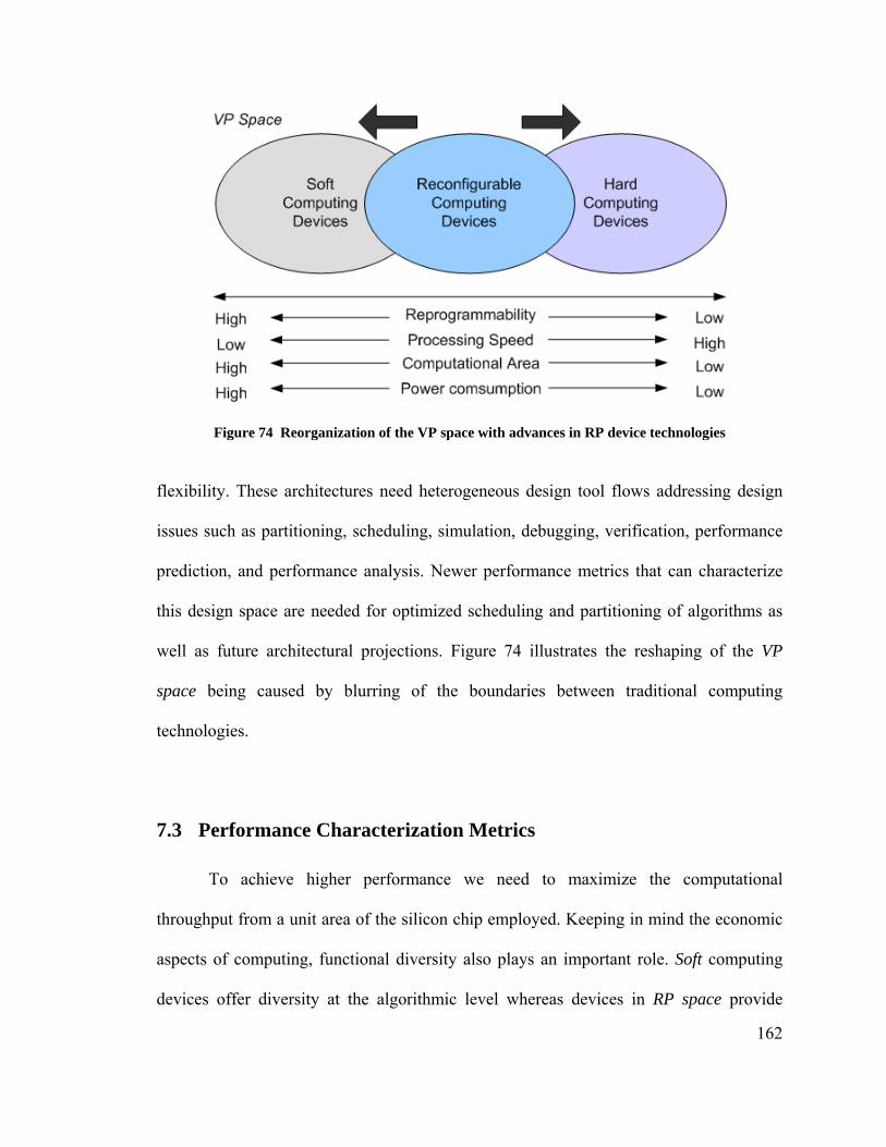
Figure 74 Reorganization of the VP space with advances in RP device technologies
flexibility. These architectures need heterogeneous design tool flows addressing design
issues such as partitioning, scheduling, simulation, debugging, verification, performance
prediction, and performance analysis. Newer performance metrics that can characterize
this design space are needed for optimized scheduling and partitioning of algorithms as
well as future architectural projections. Figure 74 illustrates the reshaping of the VP
space being caused by blurring of the boundaries between traditional computing
technologies.
7.3 Performance Characterization Metrics
To achieve higher performance we need to maximize the computational
throughput from a unit area of the silicon chip employed. Keeping in mind the economic
aspects of computing, functional diversity also plays an important role. Soft computing
devices offer diversity at the algorithmic level whereas devices in RP space provide
162
functional diversity at a lower level of abstraction, typically at the logic circuit level. It is
generally understood that fixed functional configurations as in custom hard computing
devices such as ASICs occupy the upper bound of performance in terms of computational
throughput, power consumption, and area required on the silicon. The performance based
on the above three metrics reduces as we move across the computing space towards soft
computing devices. The metrics introduced here for our analysis compare performance as
a function of speed, area, and power required for implementing the computational task on
a computational device. Some of the concepts used have been introduced and explained
in detail in [212, 213]. These metrics can be used to characterize the computing devices
in the VP space with respect to computational tasks. They help to maximize performance
of heterogeneous computing platforms that strive to maximize performance based on
resource and application specific constraints. These also serve as a guide for future
architectural projections.
7.3.1 Computational Device Capacity
Computational device capacity is the measure of computational work per unit
time that can be extracted from a computational device structure. Thus, if a device offers
computational capacity then it can complete N computations in time: capD
capDNT = (26)
163
The above equation raises two questions:
(i) How do we characterize computations of computing tasks?
(ii) How do we characterize tasks?
Tasks are difficult to generalize and are application specific. They may be
grouped into sets with common features and used for analysis. Computations are task
specific. If the application tasks are grouped using types of computations as a feature, the
device computational capacities can be calculated specific to a set of computational tasks.
Thus, if a computing device offers computational capacity then it can
complete computations in time:
taskcapD _
taskN
taskcap
tasktask D
NT
_= (27)
If the computational tasks are grouped using floating point operations as a feature
then the device computational capacity gives the floating operations per second (FLOPS),
a metric widely used in measuring performance of computing systems.
(sec)_task
FLOPFLOPScap T
ND = (28)
If the grouped tasks represent neuromorphic circuits, the computation of interest
is synaptic connections processed. Thus, the computational capacity will indicate
synaptic connections processed per second or CPS, another widely used metric used for
measuring performance of neuromorphic circuits.
164
(sec)_
__task
connsynconnsyncap T
ND = (29)
To calculate raw throughput of tasks on computational devices Dehon [212]
suggested using a gate evaluation metric. The idea is to count the number of gate
evaluations in a minimal logic circuit required to implement the computational task.
Thus, if a device offers capacity to an application task requiring gate
evaluations, the task can be completed in time:
gecapD _ geN
gecap
getask D
NT
_= (30)
7.3.2 Computational Density
Computational density (or functional density) can be defined as computational
capacity per unit area. This is a space-time metric that is measured in terms of the number
of operations per unit space-time. Thus, computational density can be calculated as
shown below.
AD
F capdensity = (31)
165
Area A in the above equation is the silicon area used for providing the device
computational capacity to the task. This is fabrication process dependent and varies with
the feature size used in the fabrication process. Thus, the same computation implemented
using a smaller feature size will have higher computational density as compared to a
fabrication process using larger feature size. To make our calculations independent of this
parameter, we normalize area in units of λ, half the minimum feature size of the
fabrication process. Thus the metric for computational density is measured in units of
operations/ λ2s.
)( 2λAT
NF
task
opsdensity
×= (32)
Thus, in the case of general purpose computing devices such as processors, the
area is the silicon area used for the implementation of instructions in the computational
task. This includes the area occupied by the datapath elements, interconnections, and
internal memory. In case of an ASIC, it is the chip area occupied by the logic gates and
interconnections of the logic circuit used for implementation of the computational task.
For an FPGA, it is the chip area occupied by the total number of logic blocks and the
routing circuits used by the computational task.
7.3.3 Power Efficiency
Delay and area have been addressed by the device capacity and density metrics,
but another important aspect of performance evaluation is power consumption. This is an
important factor in HPC systems, but is critical in many high performance embedded
computing systems. Dynamic power dissipation is directly related to the yielded device
capacity via the cycle frequency. The higher the frequency, the higher the dynamic power
166
dissipation will be. Thus, it is interesting to note the device capacity per unit watt (or
milli-watt) as shown below.
)(mWPD
Dd
capmWpercap =−− (33)
7.3.4 Discussion
The above metrics are indicators of computational capacity and density of a
computational device from a logic-centric view. They largely ignore the impact of the
associated interconnect and routing costs. For computational structures implementing
custom dataflow architectures the interconnect costs can substantially grow with
increasing problem sizes. For example, consider a feedforward fully connected neural
network implemented as a directed acyclic graph with neural processing elements as
nodes on an ASIC or an FPGA. Growth in network size exponentially increases the
number of synaptic interconnections, equally increasing the associated interconnect and
routing costs. These effects are more pronounced with multi-dimensional networks. This
can significantly affect the functional density estimates, and more so in RC
implementations where logic circuits are routed via pre-fabricated multiple-length
programmable routing interconnects. But these costs are difficult to generalize and
quantify and they vary depending on the computing device technology used for
implementation. For the purposes of our analysis here we will largely ignore these costs.
In case of a 2-dimensional BbNN implementation, the topological restrictions in
architecture limit the interconnect growth to linear for every additional row or column
167
added to the existing grid. Hence, the effects of ignoring the interconnect costs will be
tolerable for this particular neural network topology. But the comparison with other fully
connected networks such as multilayer perceptrons (MLP) will skew our analysis as the
device capacity may not increase linearly with increases in the size of the network. Also,
ignored in the above analysis are the data I/O rates and the memory hierarchy effects.
These will impact the actual computational throughput and device capacity in practice.
Future work should address these issues.
7.4 BbNN Performance Analysis
Our goal here is to analyze and characterize BbNN implementations on different
computing structures ranging from general purpose processors to custom computing
devices. We will characterize and compare the computational capacities and densities
provided by various computational devices to BbNN architecture in units of connections
processed per second as shown in the equations above. For a BbNN, the maximum
number of connections that can be processed per block computation is 6 as in the case of
a 2-input / 2-output neuron block. Equation below shows the neuron block computation
in the case of a 2/2 block.
.2,1,.12
1=⎟
⎟⎠
⎞⎜⎜⎝
⎛∑+==
kxwbgyj
jjkkk (34)
168
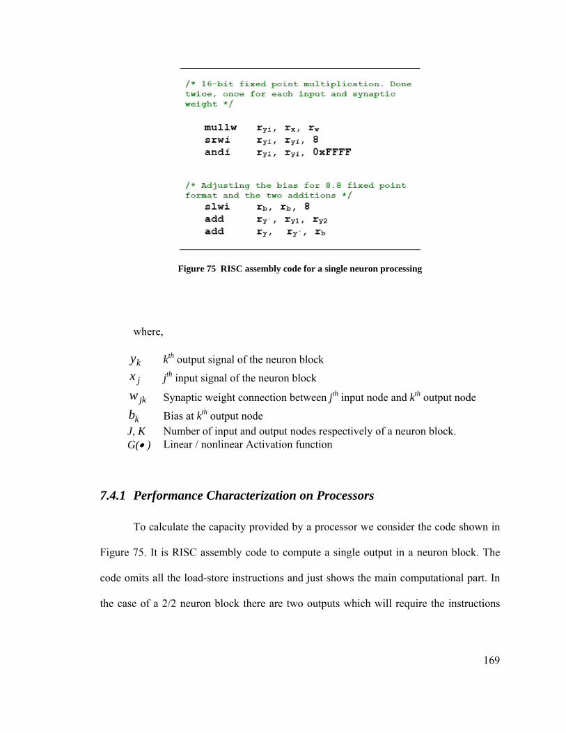
Figure 75 RISC assembly code for a single neuron processing
where,
ky kth output signal of the neuron block
jx jth input signal of the neuron block
jkw Synaptic weight connection between jth input node and kth output node
kb Bias at kth output node J, K Number of input and output nodes respectively of a neuron block. G(• ) Linear / nonlinear Activation function
7.4.1 Performance Characterization on Processors
To calculate the capacity provided by a processor we consider the code shown in
Figure 75. It is RISC assembly code to compute a single output in a neuron block. The
code omits all the load-store instructions and just shows the main computational part. In
the case of a 2/2 neuron block there are two outputs which will require the instructions
169
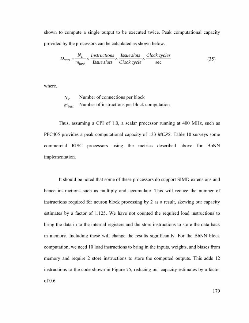
It should be noted that some of these processors do support SIMD extensions and
hence instructions such as multiply and accumulate. This will reduce the number of
instructions required for neuron block processing by 2 as a result, skewing our capacity
estimates by a factor of 1.125. We have not counted the required load instructions to
bring the data in to the internal registers and the store instructions to store the data back
in memory. Including these will change the results significantly. For the BbNN block
computation, we need 10 load instructions to bring in the inputs, weights, and biases from
memory and require 2 store instructions to store the computed outputs. This adds 12
instructions to the code shown in Figure 75, reducing our capacity estimates by a factor
of 0.6.
where,
shown to compute a single output to be executed twice. Peak computational capacity
provided by the processors can be calculated as shown below.
Thus, assuming a CPI of 1.0, a scalar processor running at 400 MHz, such as
PPC405 provides a peak computational capacity of 133 MCPS. Table 10 surveys some
commercial RISC processors using the metrics described above for BbNN
implementation.
seccyclesClock
cycleClockslotsIssue
slotsIssuensInstructio
mN
Dinst
ccap ×××=
cN
instm Number of connections per block
Number of instructions per block computation
(35)
170
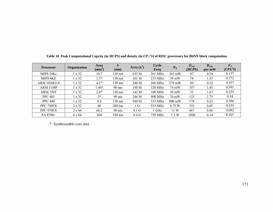
171
Table 10 Peak Computational Capcity (in MCPS) and density (in CPλ2S) of RISC processors for BbNN block computation
Processor Organization Area (mm2)
λ (nm) Area (λ2) Cycle
Freq Pd Dcap (MCPS)
Dcap per mW
Fd (CPλ2S)
MIPS 24Kc 1 x 32 10.7 130 nm 633 M 261 MHz 363 mW 87 0.24 0.137 MIPS 4KE 1 x 32 1.7* 130 nm 101 M 233 MHz 58 mW 78 1.33 0.772
ARM 1026EJ-S 1 x 32 4.2* 130 nm 248 M 266 MHz 279 mW 89 0.32 0.357 ARM 11MP 1 x 32 1.46* 90 nm 180 M 320 MHz 74 mW 107 1.45 0.591 ARM 720T 1 x 32 2.4* 130 nm 142 M 100 MHz 20 mW 33 1.67 0.235
PPC 405 1 x 32 2* 90 nm 246 M 400 MHz 76 mW 133 1.75 0.54 PPC 440 1 x 32 9.8 130 nm 580 M 533 MHz 800 mW 178 0.22 0.306
PPC 750FX 2 x 32 40 200 nm 1 G 533 MHz 6.75 W 355 0.05 0.355 PPC 970FX 2 x 64 66.2 90 nm 8.1 G 1 GHz 11 W 667 0.06 0.082 PA 8700+ 4 x 64 304 180 nm 9.4 G 750 MHz 7.1 W 1000 0.14 0.107
* Synthesizable core area
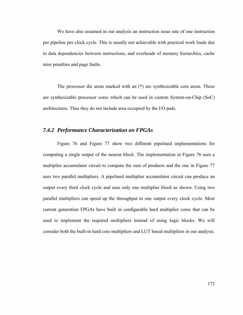
172
We have also assumed in our analysis an instruction issue rate of one instruction
per pipeline per clock cycle. This is usually not achievable with practical work loads due
to data dependencies between instructions, and overheads of memory hierarchies, cache
miss penalties and page faults.
The processor die areas marked with an (*) are synthesizable core areas. These
are synthesizable processor cores which can be used in custom System-on-Chip (SoC)
architectures. Thus they do not include area occupied by the I/O pads.
7.4.2 Performance Characterization on FPGAs
Figure 76 and Figure 77 show two different pipelined implementations for
computing a single output of the neuron block. The implementation in Figure 76 uses a
multiplier accumulator circuit to compute the sum of products and the one in Figure 77
uses two parallel multipliers. A pipelined multiplier accumulator circuit can produce an
output every third clock cycle and uses only one multiplier block as shown. Using two
parallel multipliers can speed up the throughput to one output every clock cycle. Most
current generation FPGAs have built in configurable hard multiplier cores that can be
used to implement the required multipliers instead of using logic blocks. We will
consider both the built-in hard core multipliers and LUT based multipliers in our analysis.
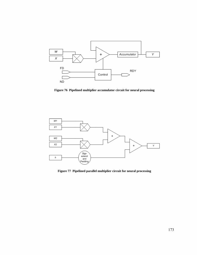
Figure 76 Pipelined multiplier accumulator circuit for neural processing
Figure 77 Pipelined parallel multiplier circuit for neural processing
173
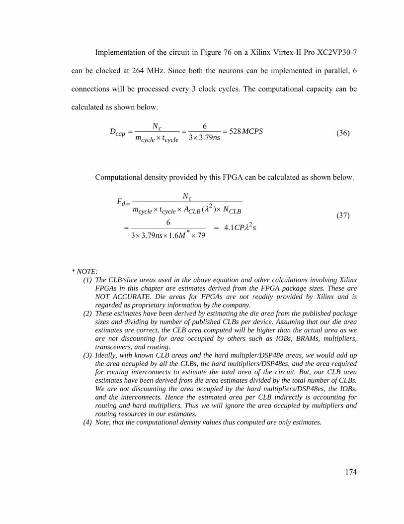
Implementation of the circuit in Figure 76 on a Xilinx Virtex-II Pro XC2VP30-7
can be clocked at 264 MHz. Since both the neurons can be implemented in parallel, 6
connections will be processed every 3 clock cycles. The computational capacity can be
calculated as shown below.
MCPSnstm
ND
cyclecycle
ccap 528
79.336
=×
=×
= (36)
Computational density provided by this FPGA can be calculated as shown below.
sCPMns
NAtm
NF
CLBCLBcyclecycle
cd
2*
2
1.4796.179.33
6
)(
λ
λ
=×××
=
×××=
(37)
* NOTE: (1) The CLB/slice areas used in the above equation and other calculations involving Xilinx
FPGAs in this chapter are estimates derived from the FPGA package sizes. These are NOT ACCURATE. Die areas for FPGAs are not readily provided by Xilinx and is regarded as proprietary information by the company.
(2) These estimates have been derived by estimating the die area from the published package sizes and dividing by number of published CLBs per device. Assuming that our die area estimates are correct, the CLB area computed will be higher than the actual area as we are not discounting for area occupied by others such as IOBs, BRAMs, multipliers, transceivers, and routing.
(3) Ideally, with known CLB areas and the hard multipler/DSP48e areas, we would add up the area occupied by all the CLBs, the hard multipliers/DSP48es, and the area required for routing interconnects to estimate the total area of the circuit. But, our CLB area estimates have been derived from die area estimates divided by the total number of CLBs. We are not discounting the area occupied by the hard multipliers/DSP48es, the IOBs, and the interconnects. Hence the estimated area per CLB indirectly is accounting for routing and hard multipliers. Thus we will ignore the area occupied by multipliers and routing resources in our estimates.
(4) Note, that the computational density values thus computed are only estimates.
174

175
Table 11 shows the computed capacity and density values for BbNNs provided by
some selected FPGAs. It should be noted that the area, and speed values are obtained
using Xilinx synthesis, and place and route tools (ISE v7.1) [214].
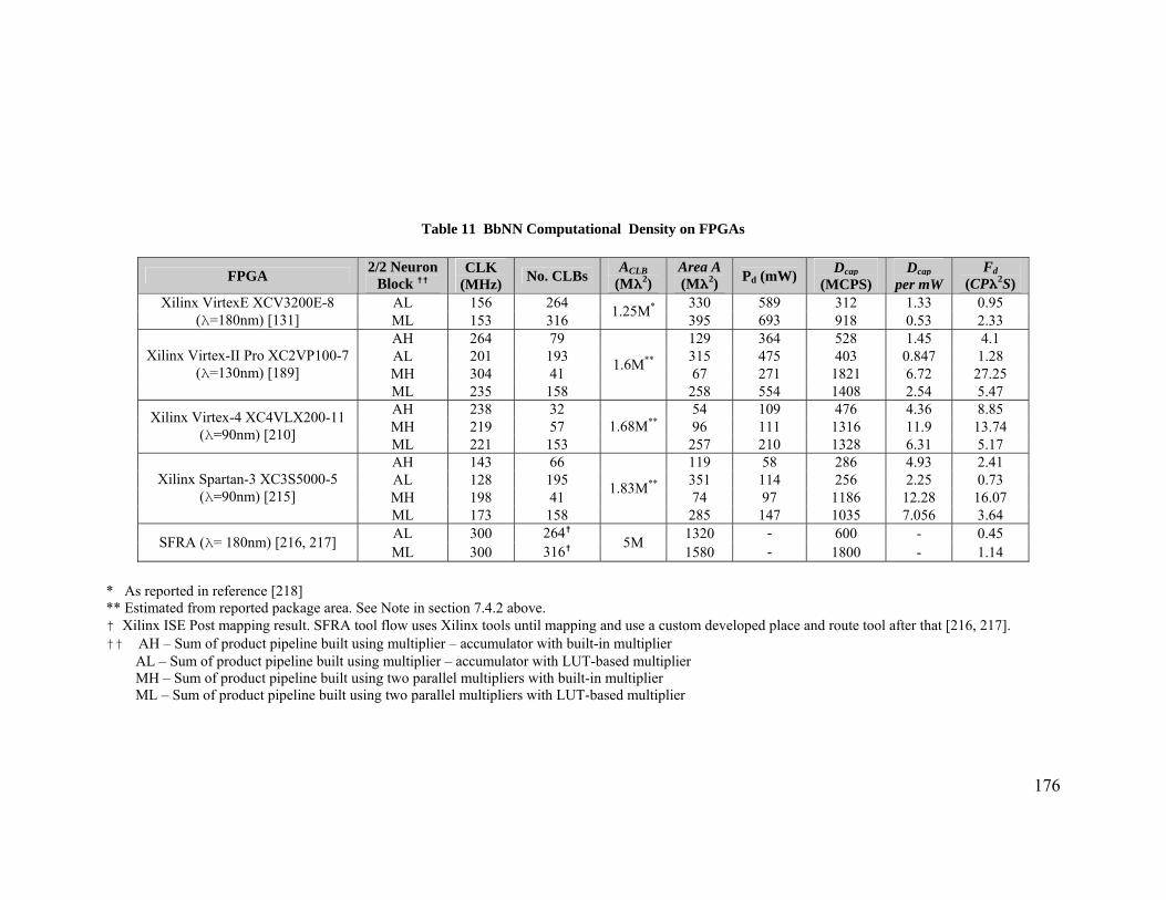
176
Table 11 BbNN Computational Density on FPGAs
FPGA 2/2 Neuron Block ††
CLK (MHz) No. CLBs ACLB
(Mλ2) Area A (Mλ2) Pd (mW) Dcap
(MCPS) Dcap
per mW Fd
(CPλ2S) AL 156 264 330 589 312 1.33 0.95Xilinx VirtexE XCV3200E-8
(λ=180nm) [131] ML 153 316 1.25M* 395 693 918 0.53 2.33AH 264 79 129 364 528 1.45 4.1AL 201 193 315 475 403 0.847 1.28MH 304 41 67 271 1821 6.72 27.25
Xilinx Virtex-II Pro XC2VP100-7 (λ=130nm) [189]
ML 235 158
1.6M**
258 554 1408 2.54 5.47AH 238 32 54 109 476 4.36 8.85MH 219 57 96 111 1316 11.9 13.74Xilinx Virtex-4 XC4VLX200-11
(λ=90nm) [210] ML 221 153
1.68M** 257 210 1328 6.31 5.17
AH 143 66 119 58 286 4.93 2.41AL 128 195 351 114 256 2.25 0.73MH 198 41 74 97 1186 12.28 16.07
Xilinx Spartan-3 XC3S5000-5 (λ=90nm) [215]
ML 173 158
1.83M**
285 147 1035 7.056 3.64AL - 300 264† 1320 - 600 0.45SFRA (λ= 180nm) [216, 217] ML 300 316† 5M
1580 - 1800 - 1.14 * As reported in reference [218] ** Estimated from reported package area. See Note in section 7.4.2 above. † Xilinx ISE Post mapping result. SFRA tool flow uses Xilinx tools until mapping and use a custom developed place and route tool after that [216, 217]. †† AH – Sum of product pipeline built using multiplier – accumulator with built-in multiplier AL – Sum of product pipeline built using multiplier – accumulator with LUT-based multiplier MH – Sum of product pipeline built using two parallel multipliers with built-in multiplier ML – Sum of product pipeline built using two parallel multipliers with LUT-based multiplier
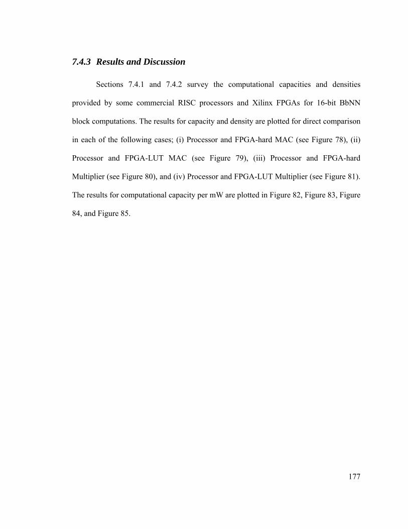
177
7.4.3 Results and Discussion
Sections 7.4.1 and 7.4.2 survey the computational capacities and densities
provided by some commercial RISC processors and Xilinx FPGAs for 16-bit BbNN
block computations. The results for capacity and density are plotted for direct comparison
in each of the following cases; (i) Processor and FPGA-hard MAC (see Figure 78), (ii)
Processor and FPGA-LUT MAC (see Figure 79), (iii) Processor and FPGA-hard
Multiplier (see Figure 80), and (iv) Processor and FPGA-LUT Multiplier (see Figure 81).
The results for computational capacity per mW are plotted in Figure 82, Figure 83, Figure
84, and Figure 85.
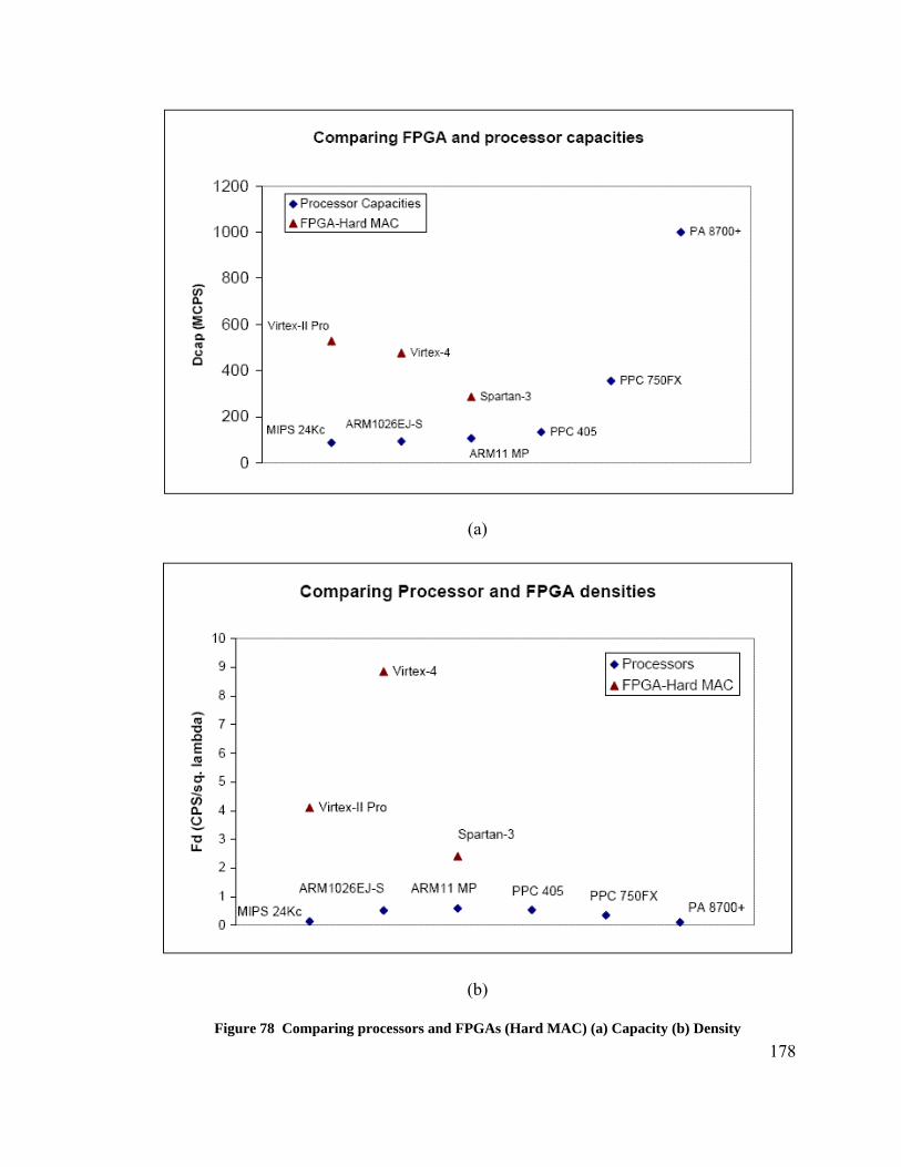
(a)
(b)
Figure 78 Comparing processors and FPGAs (Hard MAC) (a) Capacity (b) Density 178
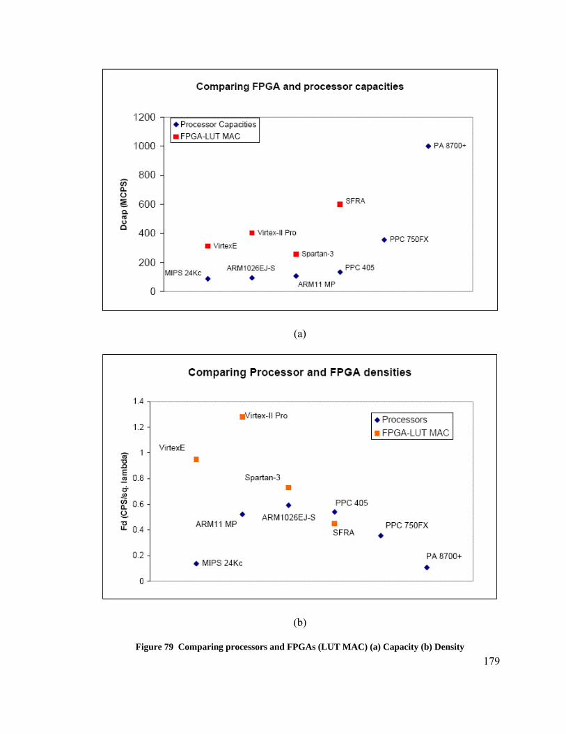
(a)
(b)
Figure 79 Comparing processors and FPGAs (LUT MAC) (a) Capacity (b) Density 179
(a)
(b)
Figure 80 Comparing processors and FPGAs (Hard Multipliers) (a) Capacity (b) Density
180
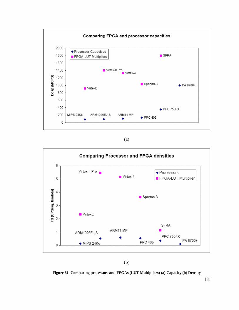
(a)
(b)
Figure 81 Comparing processors and FPGAs (LUT Multipliers) (a) Capacity (b) Density
181
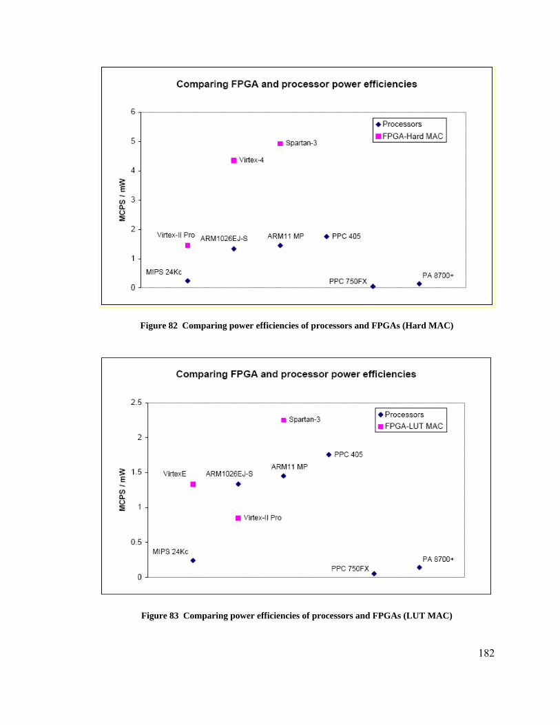
Figure 82 Comparing power efficiencies of processors and FPGAs (Hard MAC)
Figure 83 Comparing power efficiencies of processors and FPGAs (LUT MAC)
182
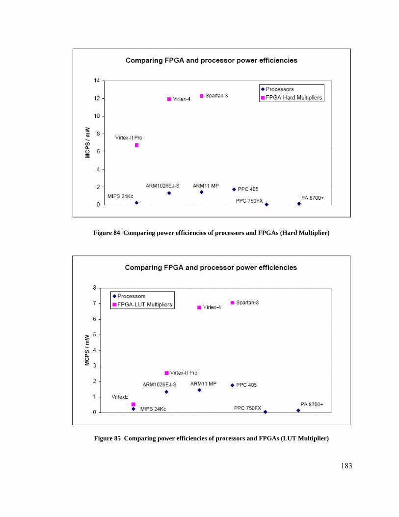
Figure 84 Comparing power efficiencies of processors and FPGAs (Hard Multiplier)
Figure 85 Comparing power efficiencies of processors and FPGAs (LUT Multiplier)
183
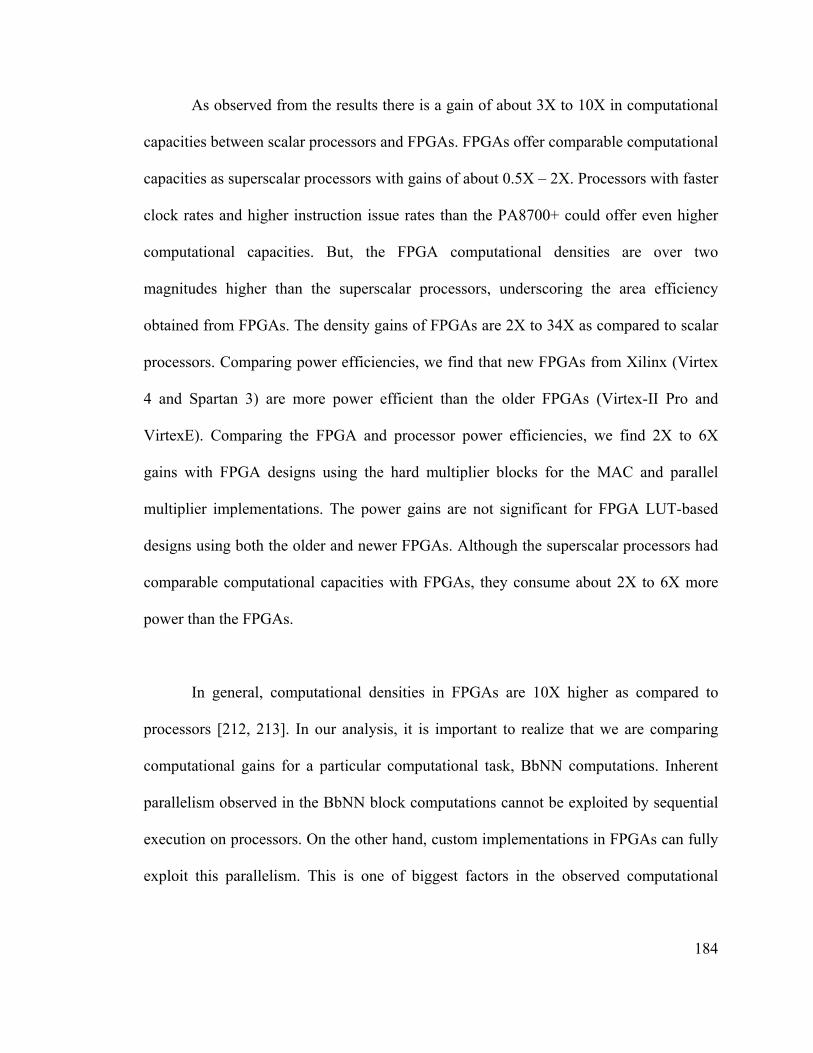
184
As observed from the results there is a gain of about 3X to 10X in computational
capacities between scalar processors and FPGAs. FPGAs offer comparable computational
capacities as superscalar processors with gains of about 0.5X – 2X. Processors with faster
clock rates and higher instruction issue rates than the PA8700+ could offer even higher
computational capacities. But, the FPGA computational densities are over two
magnitudes higher than the superscalar processors, underscoring the area efficiency
obtained from FPGAs. The density gains of FPGAs are 2X to 34X as compared to scalar
processors. Comparing power efficiencies, we find that new FPGAs from Xilinx (Virtex
4 and Spartan 3) are more power efficient than the older FPGAs (Virtex-II Pro and
VirtexE). Comparing the FPGA and processor power efficiencies, we find 2X to 6X
gains with FPGA designs using the hard multiplier blocks for the MAC and parallel
multiplier implementations. The power gains are not significant for FPGA LUT-based
designs using both the older and newer FPGAs. Although the superscalar processors had
comparable computational capacities with FPGAs, they consume about 2X to 6X more
power than the FPGAs.
In general, computational densities in FPGAs are 10X higher as compared to
processors [212, 213]. In our analysis, it is important to realize that we are comparing
computational gains for a particular computational task, BbNN computations. Inherent
parallelism observed in the BbNN block computations cannot be exploited by sequential
execution on processors. On the other hand, custom implementations in FPGAs can fully
exploit this parallelism. This is one of biggest factors in the observed computational
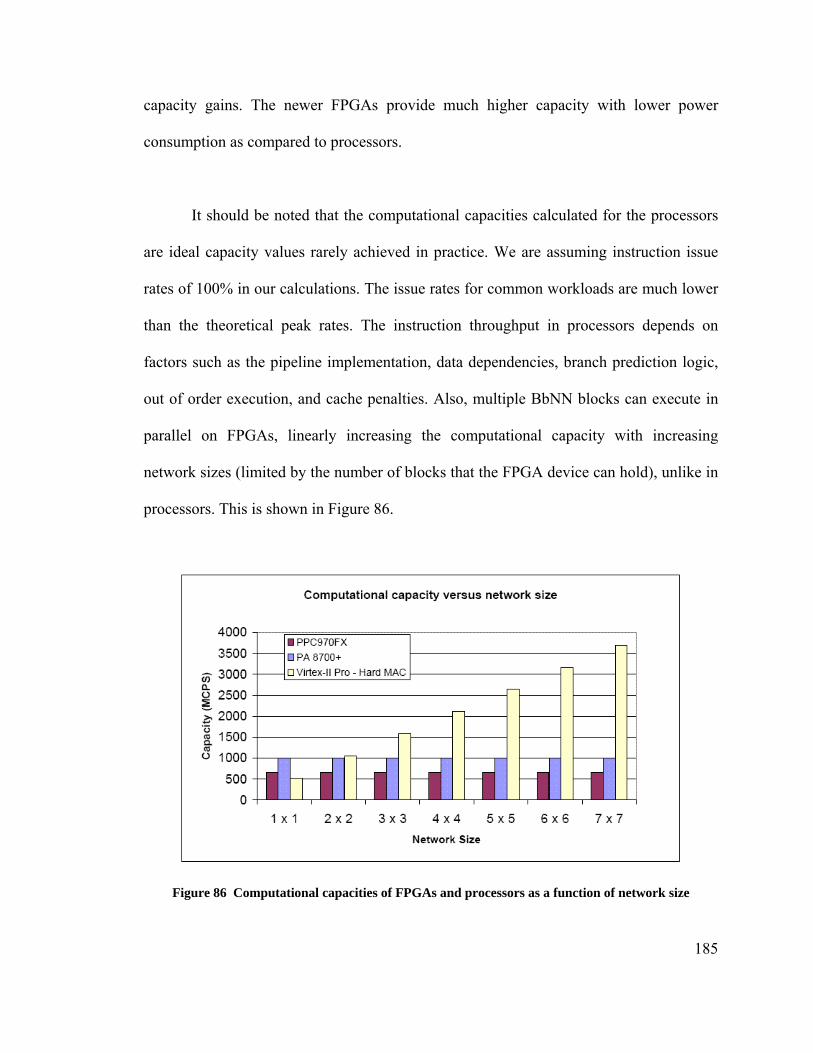
capacity gains. The newer FPGAs provide much higher capacity with lower power
consumption as compared to processors.
It should be noted that the computational capacities calculated for the processors
are ideal capacity values rarely achieved in practice. We are assuming instruction issue
rates of 100% in our calculations. The issue rates for common workloads are much lower
than the theoretical peak rates. The instruction throughput in processors depends on
factors such as the pipeline implementation, data dependencies, branch prediction logic,
out of order execution, and cache penalties. Also, multiple BbNN blocks can execute in
parallel on FPGAs, linearly increasing the computational capacity with increasing
network sizes (limited by the number of blocks that the FPGA device can hold), unlike in
processors. This is shown in Figure 86.
Figure 86 Computational capacities of FPGAs and processors as a function of network size
185
186
7.4.4 Performance of SBbNs
The smart block-based neuron (SBbN) design presented in 5 is the one used in our
implementation of intrinsically evolvable BbNNs. Section 5.4 presents the performance
results for the design. The design can achieve 147MCPS on Virtex-II Pro at frequency of
245MHz. Why is the computational capacity low compared to the results presented in
section 7.4.2? The reasoning for this is as below.
♦ SBbN design is larger than the basic neuron design considered in section 7.4.2.
The design is larger to accommodate for the extra logic required for the dynamic
configuration adaptability, activation function lookup table, register storage for
weights and biases, and the extra multipliers required to accommodate for 1-input
/ 3-outputs neuron block configuration.
♦ Use of a multiply-accumulator unit instead of parallel multipliers also affects the
throughput. The choice to sacrifice the throughput was made to enable the FPGA
to hold larger networks. Using parallel multipliers would require twice the
number of hard multipliers per neuron block as compared to the MAC based
approach. Thus, the fixed number of multipliers available per FPGA quickly
becomes a bottleneck for network scalability.
♦ P/T net-based dataflow implementation adopted for reliable asynchronous
intercommunication between neuron blocks has one side effect. It enforces serial
execution of the neuron block computation. Although, each of outputs within the
neuron block compute in parallel. New inputs cannot be applied until the previous
inputs are consumed and corresponding outputs generated by the neuron block.
Also, the cycle to lookup the activation function value in the lookup table adds to
the computation time. In total requiring 10 clock cycles to produce a result at the
output. At 245 MHz with a maximum of 6 connections processed in a given block
computation the throughput is 147MCPS per neuron block. The computational
density with the occupied area of 171 CLBs on Virtex-II Pro (XC2VP30) FPGA
is 0.54 connections per λ2s.
As shown in Figure 86, it should be noted that the computational capacity
increases linearly with increase in the network size, unlike the processors. Thus, for an m
× n network size the peak computational capacity is 147n MCPS.
7.5 Model Sensitivity to Parametric Variations
Analysis presented above is based on certain parametric value estimations such as
the CLB area which has been estimated using the published package sizes of FPGA
devices. It is important to analyze the sensitivity of our model to variations in model
parameters. The analysis is presented below.
Let Mc be the ideal value of the function computed using model M and Md be the
observed value due to variation in parameter p from ideal to the observed value. If the
deviation factor is dp then,
p
cd d
MM = (38)
187
Thus, error in model computation is
⎟⎟⎠
⎞⎜⎜⎝
⎛−=−=
pcdc d
MMMe 11 (39)
The percent deviation from the ideal value can be computed as shown below.
10011 ×⎟⎟⎠
⎞⎜⎜⎝
⎛−=
pdE (40)
For example, deviation in peak computational capacity of a processor due to
variation in observed CPI from assumed ideal value can be
calculated as shown below.
( actualCPI ) ( )estimatedCPI
estimated
actualcpi CPI
CPId = (41)
10011 ×⎟⎟⎠
⎞⎜⎜⎝
⎛−=
cpidE (42)
Deviation in observed computational density in an FPGA to variation in CLB area
can be computed as shown below.
A
dd d
FF estimated
actual= (43)
where,
188
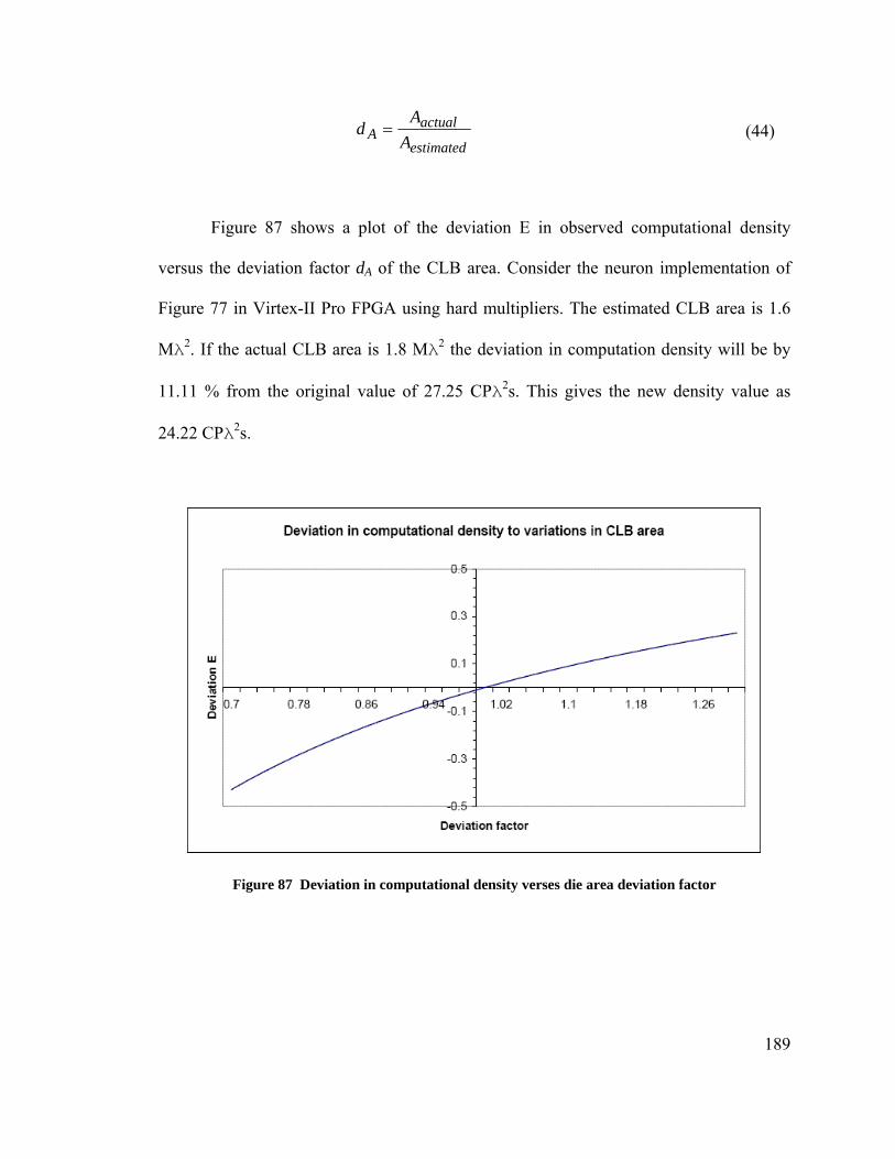
estimated
actualA A
Ad = (44)
Figure 87 shows a plot of the deviation E in observed computational density
versus the deviation factor dA of the CLB area. Consider the neuron implementation of
Figure 77 in Virtex-II Pro FPGA using hard multipliers. The estimated CLB area is 1.6
Mλ2. If the actual CLB area is 1.8 Mλ2 the deviation in computation density will be by
11.11 % from the original value of 27.25 CPλ2s. This gives the new density value as
24.22 CPλ2s.
Figure 87 Deviation in computational density verses die area deviation factor
189
190
7.6 Summary
A performance characterization model for BbNNs was presented in this chapter. It
enables performance comparison across different computational devices based on the
metrics of computational capacity and density. Computational capacity is the
computational work that can be extracted from a computational device and can be
modeled as number of operations per second. Computational density is a space-time
metric giving the computational work extracted per unit time and area from a
computational device. Computational density per watt gives the estimate of power
consumption for the execution of the computation. These metrics were used to analyze
the BbNN computational capacity on the RISC processors and the FPGAs. The results
show FPGAs provide on an average 10X higher computational capacities than the scalar
RISC processors for a single BbNN block. The computational densities of FPGAs are 2X
to 34X higher than the processors. The computational capacity of FPGAs linearly
increases with the increasing network sizes, unlike processors. The newer FPGAs from
Xilinx (the Virtex 4 and the Spartan 3) are more power efficient than the older FPGAs.
Comparing their power efficiencies with processors, we observe 2X to 6X higher
computational capacities per mW provided by FPGAs. Although the superscalar
processors had comparable computational capacities with FPGAs for a single neuron
block computation, FPGAs consume about 2X to 6X less power and provide 2X to 34X
gains in computational densities. Model’s sensitivity to variations in its parameters has
also been analyzed and presented. The deviation in computed values is found to vary
linearly to parametric variations.
8 SUMMARY AND CONCLUSIONS
Following list summarizes the major points, concepts, and accomplishments of
this work.
♦ Evolvable hardware systems (EHW) use reconfigurable computing platforms such
as FPGAs to evolve hardware circuitry under the control of evolutionary
algorithms. The configuration bitstream is encoded as a genotype and evolved
over multiple generations to find a network that meets the target fitness. Fitness is
determined using an objective function that includes parameters such as
correctness of circuit functionality, area, speed, and power.
♦ Intrinsic and extrinsic hardware evolutions are classifications of evolvable
hardware systems based on the role of reconfigurable computing (RC) hardware
in evolution. Intrinsic systems include the hardware in the evolution loop to
measure the fitness of the genotype. Hence they perform online evolution.
Extrinsic systems use a software model of the hardware and perform offline
evolution using computer simulations.
♦ Functional-level and gate-level evolution describe the abstraction level at which
the evolution is performed in an evolvable hardware system. Evolving FPGA
configuration bitstream encoded as genotype in an evolutionary algorithm is
circuit-level or gate-level evolution. Evolving the interconnections and internal
191
192
parameters of higher level functional modules such as multipliers, accumulators,
and trigonometric functions is functional-level evolution.
♦ Block-based neural networks (BbNN) are grid-based networks of neuron blocks,
the basic processing elements of the network. The outputs of the network are a
unique function of the inputs, the network structure, and the synaptic weights of
the neuron blocks. Training of these networks is a multi-parametric optimization
problem, simultaneously evolving structure and synaptic weights of the neuron
blocks. Typically genetic algorithms are used to train these networks to model
input – output relationships and learn characteristic features in training datasets.
♦ Offline and online training are artificial neural network (ANN) learning schemes.
In an offline learning the neural network is trained using a batch of training data
offline. In an online learning scheme the neural network is trained on real data in
field. Online training in neural networks improves network generalization, and
enhances system reliability. The in-field re-training capability enhances ANN
system performance by adapting to variations in input data.
♦ Intrinsically evolvable BbNN hardware design is presented. The design supports
on-chip, online training of BbNNs on FPGAs, presenting a compact, and
evolvable neural network chip for applications in dynamic environments. The
BbNN on-chip training is a functional-level intrinsic evolution with neuron blocks
as the functional modules.
♦ Design Scalability in space (across multiple FPGAs) and in time (using same
FPGA in time multiplexed manner) is enabled by reliable, asynchronous dataflow
architecture implemented in the design. Asynchronous synaptic links enable
193
design scalability by ensuring reliable communication between neuron blocks
spread in time or space irrespective of the type of communication channels used
to transfer data between neuron blocks. This makes the design portable and
scalable across a heterogeneous mixture of reconfigurable computing resources.
♦ Online training algorithm for BbNN is presented along with a case study –
Adaptive neural luminosity controller. The results of the study demonstrate the
benefits of online training and showcase the applicability of the designed platform
to applications in dynamic environments.
♦ Performance characterization model of BbNN RC implementations is presented.
The model characterizes BbNN implementations across the general purpose
computing devices and the FPGAs using performance metrics such as the
computational device capacity, the computational density, and the power
efficiency. Computational device capacity is the measure of computational work
per unit time that can be extracted from a computational device structure. For
BbNNs it is the number of synaptic connections processed per second (CPS) by
the computing device. Computational density is a space-time metric and can be
defined as the computational capacity provided by the computing device per unit
silicon area. The results show FPGAs provide on an average 10X higher
computational capacities than the scalar RISC processors for a single BbNN
block. The computational densities of FPGAs are 2X to 34X higher than the
processors. The computational capacity of FPGAs linearly increases with the
increasing network sizes, unlike processors. The newer FPGAs from Xilinx (the
Virtex 4 and the Spartan 3) are more power efficient than the older FPGAs.
194
Comparing their power efficiencies with processors, we observe 2X to 6X higher
computational capacities per mW provided by FPGAs. Although the superscalar
processors had comparable computational capacities with FPGAs for a single
neuron block computation, FPGAs consume about 2X to 6X less power and
provide 2X to 34X gains in computational densities.
This work provides a platform for further research on BbNNs in three directions –
implementations, algorithms, and applications. They are discussed below.
1. Implementations
This work provides a platform for further research in custom, scalable,
intrinsically evolvable ANN implementations. The designed implementation enables
BbNN scalability across heterogeneous RC resources, but the designing and
implementing working prototypes should be undertaken as future extensions to the
project. The developed approach could also be ported to other ANN architectures such as
multilayer perceptrons and cellular neural networks. The genetic algorithm (GA)
operators in the implementation currently execute in software running on the PPC 405
embedded core on the FPGA die. This approach was chosen for the current
implementation to maximally utilize the reconfigurable logic space to fit larger networks.
But with increasing capacities of FPGAs, genetic operators can be hardware accelerated.
195
2. Algorithms
Active research should be pursued in exploring time bounded training algorithms
for BbNNs. Online learning ability significantly expands the application space of BbNNs
to dynamic environments. But many applications may require real-time performance. The
training algorithms used for BbNNs are currently not time bounded. Theoretical
investigations should be undertaken to establish confidence levels in training results
obtained within bounded times. Another important area of research in algorithms for
BbNNs is to explore reinforcement learning techniques for BbNNs. This enables BbNNs
to learn from interactions with the surrounding environment. A difficult issue to solve in
online training of artificial neural networks is measure fitness of a network when target
outputs are unknown. Reinforcement learning algorithms have a notion of reward from
environment for actions of the agent. The agent has a goal to discover the state - action
policies that maximize this reward over time.
3. Applications
The biggest selling point of any technology is in its applications. This dissertation
provides a glimpse in to the realm of possible applications of BbNNs in dynamic
environments. Applications such as speech recognition, handwriting recognition, medical
diagnostics and monitoring, and navigational systems are all possible contenders in the
application set. Further research efforts are required to investigate the feasibility of using
BbNNs for these applications.

196
The performance model presented is currently logic centric. It should be extended
to include routing and interconnect costs. Although the model is applied to BbNNs, it can
apply to other computational tasks. Our analysis compares performance on FPGAs and
processors. This should be extended to include other computing devices such as analog
and digital custom ASICs.

197
REFERENCES
REFERENCES
[1] Wikipedia, "Reconfigurable computing
(http://en.wikipedia.org/wiki/Reconfigurable_Computing)," 2007. [2] H. de Garis, "Evolvable Hardware : Principles and Practice
http://www.cs.usu.edu/~degaris/papers/CACM-E-Hard.html," 1997. [3] S. Haykin, Neural Networks: A Comprehensive Foundation, 2nd ed.: Prentice
Hall, 1998. [4] W. Jiang, S. G. Kong, and G. D. Peterson, "ECG Signal Classification using
Block-based Neural Networks," in Proceeding of International Joint Conference on Neural Networks (IJCNN-2005), 2005, pp. 992-996.
[5] W. Jiang, S. G. Kong, and G. D. Peterson, "Continuous Heartbeat Monitoring Using Evolvable Block-based Neural Networks," in Neural Networks, 2006. IJCNN '06. International Joint Conference on, 2006, pp. 1950-1957.
[6] W. Jiang, "Evolutionary Optimization of Block based Neural Networks With Application to ECG Heartbeat Classification," in Department of Electrical and Computer Engineering. vol. PhD Knoxville: University of Tennessee, 2007.
[7] R. S. Sutton and A. G. Barto, Reinforcement Learning: An Introduction: The MIT Press, 1998.
[8] A. M. Turing, "Computing machinery and Intelligence," in Mind. vol. 59, 1950, pp. 433-60.
[9] W. S. McCulloch and W. H. Pitts, "A logical calculus of the ideas immanent in nervous activity," in Bulletin of Mathematical Biophysics, 1943.
[10] D. O. Hebb, The Organization of Behavior. : Wiley, 1949. [11] F. Rosenblatt, "The Perceptron: A Probabilistic Model for Information Storage
and Organization in the Brain," Cornell Aeronautical Laboratory, Psychological Review, vol. 65, pp. 386-408, 1958.
[12] B. Widrow and M. E. Hoff, "Adaptive switching circuits," 1960 IRE WESCON Convention Record, pp. 96-104, 1960.
[13] B. Widrow and M. A. Lehr, "30 Years of Adaptive Neural Networks: Perceptron, Madaline, and Backpropagation.," in Proceedings of the IEEE, 1990, pp. 1415-1442.
[14] M. Minsky and S. Papert, Perceptrons: MIT Press, Cambridge, MA, 1969. [15] J. J. Hopfield, "Neural networks and physical systems with emergent
computational abilities.," in Proceedings of the National Academy of Sciences, 1982.
[16] R. Sutton, "Two problems with backpropagation and other steepest-descent learning procedures for networks," in Eighth Annual Conference of the Cognitive Science Society, Hillsdale, NJ, 1986, pp. 823-831.
[17] C. Jacob, J. Rehder, J. Siemandel, and A. Friedmann, "XNeuroGene: a system for evolving artificial neural networks," in Proceedings of the Third International
198
199
Workshop on Modeling, Analysis, and Simulation of Computer and Telecommunication Systems, MASCOTS '95, 1995, pp. 436-439.
[18] S. Baluja, "Evolution of an artificial neural network based autonomous land vehicle controller," Systems, Man and Cybernetics, Part B, IEEE Transactions on, vol. 26, pp. 450-463, 1996.
[19] H. Seung-Soo and G. S. May, "Optimization of neural network structure and learning parameters using genetic algorithms," in Proceedings Eighth IEEE International Conference on Tools with Artificial Intelligence. , 1996, pp. 200-206.
[20] P. G. Harrald and M. Kamstra, "Evolving artificial neural networks to combine financial forecasts," Evolutionary Computation, IEEE Transactions on, vol. 1, pp. 40-52, 1997.
[21] X. Yao and Y. Liu, "A new evolutionary system for evolving artificial neural networks," Neural Networks, IEEE Transactions on, vol. 8, pp. 694-713, 1997.
[22] C. Zhang, Y. Li, and H. Shao, "A new evolved artificial neural network and its application," in Proceedings of the 39th IEEE Conference on Decision and Control., 2000, pp. 1065-1068 vol.2.
[23] S. W. Moon and S. G. Kong, "Block-based neural networks," IEEE Transactions on Neural Networks, vol. 12, pp. 307-317, 2001.
[24] K. Kyung-Joong and C. Sung-Bae, "Evolving artificial neural networks for DNA microarray analysis," in The 2003 Congress on Evolutionary Computation, CEC '03, 2003, pp. 2370-2377 Vol.4.
[25] D. A. Miller, R. Arguello, and G. W. Greenwood, "Evolving artificial neural network structures: experimental results for biologically-inspired adaptive mutations," in Congress on Evolutionary Computation. CEC2004, 2004, pp. 2114-2119 Vol.2.
[26] J. N. H. Heemskerk, "Overview of Neural Hardware.," in Neurocomputers for Brain-Style Processing. Design, Implementation and Application: Unit of Experimental and Theoretical Psychology, Leiden University,The Netherlands., 1995.
[27] H. P. Graf and L. D. Jackel, "Advances in neural network hardware," 1988, pp. 766-769.
[28] D. R. Collins and P. A. Penz, "Considerations for neural network hardware implementations," 1989, pp. 834-836 vol.2.
[29] P. Ienne, "Architectures for neuro-computers: Review and performance evaluation," Technical Report 93/21, Swiss Federal Institute of Technology, 1993.
[30] P. Ienne and G. Kuhn, "Digital systems for neural networks," in Digital Signal Processing Technology. vol. 57, P. Papamichalis and R. Kerwin, Eds. Orlando, FL: SPIE Optical Engineering, 1995.
[31] I. Aybay, S. Cetinkaya, and U. Halici, "Classification of neural network hardware," Neural Network World, vol. Vol 6 pp. 11-29, 1996.
[32] H. C. Card, G. K. Rosendahl, D. K. McNeill, and R. D. McLeod, "Competitive learning algorithms and neurocomputer architecture," Computers, IEEE Transactions on, vol. 47, pp. 847-858, 1998.
200
[33] T. Schoenauer, A. Jahnke, U. Roth, and H. Klar, "Digital Neurohardware: Principles and Perspectives," in Proceedings of Neuronal Networks in Applications (NN'98), Magdeburg, 1998.
[34] L. M. Reyneri, "Theoretical and implementation aspects of pulse streams: an overview," 1999, pp. 78-89.
[35] B. Linares-Barranco, A. G. Andreou, G. Indiveri, and T. Shibata, "Guest editorial - Special issue on neural networks hardware implementations," Neural Networks, IEEE Transactions on, vol. 14, pp. 976-979, 2003.
[36] J. Zhu and P. Sutton, "FPGA Implementation of Neural Networks - A Survey of a Decade of Progress," in 13th International Conference on Field-Programmable Logic and Applications Lisbon, Portugal, 2003, pp. 1062-1066.
[37] N. Aibe, M. Yasunaga, I. Yoshihara, and J. H. Kim, "A probabilistic neural network hardware system using a learning-parameter parallel architecture," 2002, pp. 2270-2275.
[38] J. L. Ayala, A. G. Lomena, M. Lopez-Vallejo, and A. Fernandez, "Design of a pipelined hardware architecture for real-time neural network computations," in The 45th Midwest Symposium on Circuits and Systems, MWSCAS 2002, pp. I-419-22 vol.1.
[39] U. Ramacher, W. Raab, J. Anlauf, U. Hachmann, J. Beichter, N. Bruls, M. Wesseling, E. Sicheneder, R. Manner, J. Glass, and et al., "Multiprocessor and memory architecture of the neurocomputer SYNAPSE-1," Int J Neural Syst, vol. 4, pp. 333-6, Dec 1993.
[40] U. Ramacher, "Synapse-X: a general-purpose neurocomputer architecture," in Neural Networks, 1991. 1991 IEEE International Joint Conference on, 1991, pp. 2168-2176 vol.3.
[41] K. R. Nichols, M. A. Moussa, and S. M. Areibi, "Feasibility of Floating-Point Arithmetic in FPGA based Artificial Neural Networks," in 15th International Conference on Computer Applications in Industry and Engineering, San Diego, California, 2002.
[42] M. Moussa, S. Areibi, and K. Nichols, "On the Arithmetic Precision for Implementing Back-Propagation Networks on FPGA: A Case Study," in FPGA Implementations of Neural Networks, 2006, pp. 37-61.
[43] J. L. Holi and J. N. Hwang, "Finite precision error analysis of neural network hardware implementations," Computers, IEEE Transactions on, vol. 42, pp. 281-290, 1993.
[44] J. L. Holt and T. E. Baker, "Back propagation simulations using limited precision calculations," 1991, pp. 121-126 vol.2.
[45] J. L. Holt and J. N. Hwang, "Finite precision error analysis of neural network hardware implementations," Computers, IEEE Transactions on, vol. 42, pp. 281-290, 1993.
[46] E. Ros, E. M. Ortigosa, R. Agis, R. Carrillo, and M. Arnold, "Real-time computing platform for spiking neurons (RT-spike)," Neural Networks, IEEE Transactions on, vol. 17, pp. 1050-1063, 2006.
[47] M. Porrmann, U. Witkowski, H. Kalte, and U. Ruckert, "Implementation of artificial neural networks on a reconfigurable hardware accelerator," in
201
Proceedings of 10th Euromicro Workshop Parallel, Distributed and Network-based Processing, 2002, pp. 243-250.
[48] C. Torres-Huitzil and B. Girau, "FPGA implementation of an excitatory and inhibitory connectionist model for motion perception," in Proceedings of 2005 IEEE International Conference on Field-Programmable Technology., 2005, pp. 259-266.
[49] S. Kothandaraman, "Implementation of Block-based Neural Networks on Reconfigurable Computing Platforms," in Electrical and Computer Engineering Department. vol. MS Knoxville: University of Tennessee, 2004.
[50] D. Ferrer, R. Gonzalez, R. Fleitas, J. P. Acle, and R. Canetti, "NeuroFPGA-implementing artificial neural networks on programmable logic devices," in Proceedings of Design, Automation and Test in Europe Conference and Exhibition, 2004, pp. 218-223 Vol.3.
[51] Y. Chin Tsu, W. Wan-de, and L. Yen Tsun, "FPGA realization of a neural-network-based nonlinear channel equalizer," Industrial Electronics, IEEE Transactions on, vol. 51, pp. 472-479, 2004.
[52] Q. Wang, B. Yi, Y. Xie, and B. Liu, "The hardware structure design of perceptron with FPGA implementation," 2003, pp. 762-767 vol.1.
[53] M. M. Syiam, H. M. Klash, I. I. Mahmoud, and S. S. Haggag, "Hardware implementation of neural network on FPGA for accidents diagnosis of the multi-purpose research reactor of Egypt," in Proceedings of the 15th International Conference on Microelectronics. ICM, 2003, pp. 326-329.
[54] M. Krips, T. Lammert, and A. Kummert, "FPGA implementation of a neural network for a real-time hand tracking system," in Proceedings of the First IEEE International Workshop on Electronic Design, Test and Applications, 2002, pp. 313-317.
[55] J. Zhu, G. J. Milne, and B. K. Gunther, "Towards an FPGA based reconfigurable computing environment for neural network implementations," in Ninth International Conference on Artificial Neural Networks (ICANN 99), 1999, pp. 661-666 vol.2.
[56] S. Happe and H. G. Kranz, "Practical applications for the machine intelligent partial discharge disturbing pulse suppression system NeuroTEK II," in Eleventh International Symposium on High Voltage Engineering, 1999, pp. 37-40 vol.5.
[57] M. Marchesi, G. Orlandi, F. Piazza, and A. Uncini, "Fast neural networks without multipliers," Neural Networks, IEEE Transactions on, vol. 4, pp. 53-62, 1993.
[58] A. F. Murray and A. V. W. Smith, "Asynchronous VLSI neural networks using pulse-stream arithmetic," Solid-State Circuits, IEEE Journal of, vol. 23, pp. 688-697, 1988.
[59] P. Lysaght, J. Stockwood, J. Law, and D. Girma, "Artificial Neural Network Implementation on a Fine-Grained FPGA," in 4th International Workshop on Field-Programmable Logic and Applications, Prague, Czech Republic, 1994, pp. 421-431.
[60] H. Hikawa, "Frequency-based multilayer neural network with on-chip learning and enhanced neuron characteristics," Neural Networks, IEEE Transactions on, vol. 10, pp. 545-553, 1999.
202
[61] H. Hikawa, "A new digital pulse-mode neuron with adjustable activation function," Neural Networks, IEEE Transactions on, vol. 14, pp. 236-242, 2003.
[62] M. van Daalen, T. Kosel, P. Jeavons, and J. Shawe-Taylor, "Emergent activation functions from a stochastic bit-stream neuron," Electronics Letters, vol. 30, pp. 331-333, 1994.
[63] E. van Keulen, S. Colak, H. Withagen, and H. Hegt, "Neural network hardware performance criteria," 1994, pp. 1955-1958 vol.3.
[64] H. O. Johansson, P. Larsson, P. Larsson-Edefors, and C. Svensson, "A 200-MHz CMOS bit-serial neural network," 1994, pp. 312-315.
[65] M. Gschwind, V. Salapura, and O. Maischberger, "Space efficient neural net implementation," in Proceedings of the Second International ACM/SIGDA Workshop on Field-Programmable Gate Arrays, Berkeley, CA, 1994.
[66] G. P. K. Economou, E. P. Mariatos, N. M. Economopoulos, D. Lymberopoulos, and C. E. Goutis, "FPGA implementation of artificial neural networks: an application on medical expert systems," in Proceedings of the Fourth International Conference on Microelectronics for Neural Networks and Fuzzy Systems., 1994, pp. 287-293.
[67] V. Salapura, "Neural networks using bit stream arithmetic: a space efficient implementation," in IEEE International Symposium on Circuits and Systems. ISCAS '94., 1994, pp. 475-478 vol.6.
[68] N. Chujo, S. Kuroyanagi, S. Doki, and S. Okuma, "An iterative calculation method of neuron model with sigmoid function," 2001, pp. 1532-1537 vol.3.
[69] S. A. Guccione and M. J. Gonzalez, "Neural network implementation using reconfigurable architectures," in Selected papers from the Oxford 1993 international workshop on field programmable logic and applications on More FPGAs Oxford, United Kingdom: Abingdon EE\&CS Books, 1994.
[70] L. Mintzer, "Digital filtering in FPGAs," in 1994 Conference Record of the Twenty-Eighth Asilomar Conference on Signals, Systems and Computers., 1994, pp. 1373-1377 vol.2.
[71] T. Szabo, L. Antoni, G. Horvath, and B. Feher, "A full-parallel digital implementation for pre-trained NNs," in Proceedings of the IEEE-INNS-ENNS International Joint Conference on Neural Networks, IJCNN 2000., 2000, pp. 49-54 vol.2.
[72] B. Noory and V. Groza, "A reconfigurable approach to hardware implementation of neural networks," in IEEE CCECE Canadian Conference on Electrical and Computer Engineering, 2003, pp. 1861-1864 vol.3.
[73] E. Pasero and M. Perri, "Hw-Sw codesign of a flexible neural controller through a FPGA-based neural network programmed in VHDL," in Proceedings of IEEE International Joint Conference on Neural Networks., 2004, pp. 3161-3165 vol.4.
[74] K. Chih-hsien, M. J. Devaney, K. Chih-ming, H. Chung-ming, W. Yi-jen, and K. Chien-ting, "The VLSI implementation of an artificial neural network scheme embedded in an automated inspection quality management system," in Proceedings of the 19th IEEE Instrumentation and Measurement Technology Conference, IMTC, 2002, pp. 239-244 vol.1.
203
[75] J. G. Eldredge and B. L. Hutchings, "Density enhancement of a neural network using FPGAs and run-time reconfiguration," in Proceedings of IEEE Workshop on FPGAs for Custom Computing Machines, 1994, pp. 180-188.
[76] J. G. Eldredge and B. L. Hutchings, "RRANN: a hardware implementation of the backpropagation algorithm using reconfigurable FPGAs," in Neural Networks, 1994. IEEE World Congress on Computational Intelligence., 1994 IEEE International Conference on, 1994, pp. 2097-2102 vol.4.
[77] C. E. Cox and W. E. Blanz, "GANGLION-a fast field-programmable gate array implementation of a connectionist classifier," IEEE Journal of Solid-State Circuits, vol. 27, pp. 288-299, 1992.
[78] A. Perez-Uribe and E. Sanchez, "Speeding-up adaptive heuristic critic learning with FPGA-based unsupervised clustering," in IEEE International Conference on Evolutionary Computation., 1997, pp. 685-689.
[79] A. Perez-Uribe and E. Sanchez, "FPGA implementation of an adaptable-size neural network," in Proceedings of The VI International Conference on Artificial Neural Networks, ICANN96, 1996.
[80] A. Perez-Uribe and E. Sanchez, "Implementation of neural constructivism with programmable hardware," in International Symposium on Neuro-Fuzzy Systems, AT'96., 1996, pp. 47-54.
[81] H. F. Restrepo, R. Hoffmann, A. Perez-Uribe, C. Teuscher, and E. Sanchez, "A networked FPGA-based hardware implementation of a neural network application," in IEEE Symposium on Field-Programmable Custom Computing Machines, 2000, pp. 337-338.
[82] T. Kurokawa and H. Yamashita, "Bus connected neural network hardware system," Electronics Letters, vol. 30, pp. 979-980, 1994.
[83] S. Guccione and M. J. Gonzalez, "Classification and Performance of Reconfigurable Architectures," in Proceedings of the 5th International Workshop on Field-Programmable Logic and Applications: Springer-Verlag, 1995.
[84] I. Kajitani, M. Murakawa, D. Nishikawa, H. Yokoi, N. Kajihara, M. Iwata, D. Keymeulen, H. Sakanashi, and T. Higuchi, "An evolvable hardware chip for prosthetic hand controller," in Proceedings of the Seventh International Conference on Microelectronics for Neural, Fuzzy and Bio-Inspired Systems, MicroNeuro '99. , 1999, pp. 179-186.
[85] K. Mathia and J. Clark, "On neural network hardware and programming paradigms," 2002, pp. 2692-2697.
[86] J. D. Hadley and B. L. Hutchings, "Design methodologies for partially reconfigured systems," in Proceedings of IEEE Symposium on FPGAs for Custom Computing Machines. , 1995, pp. 78-84.
[87] R. Gadea, J. Cerda, F. Ballester, and A. Macholi, "Artificial neural network implementation on a single FPGA of a pipelined on-line backpropagation," 2000, pp. 225-230.
[88] K. Paul and S. Rajopadhye, "Back-Propagation Algorithm Achieving 5 Gops on the Virtex-E," in FPGA Implementations of Neural Networks, 2006, pp. 137-165.
[89] U. Witkowski, T. Neumann, and U. Ruckert, "Digital hardware realization of a hyper basis function network for on-line learning," 1999, pp. 205-211.
204
[90] M. Murakawa, S. Yoshizawa, I. Kajitani, X. Yao, N. Kajihara, M. Iwata, and T. Higuchi, "The GRD chip: genetic reconfiguration of DSPs for neural network processing," Computers, IEEE Transactions on, vol. 48, pp. 628-639, 1999.
[91] D. Hammerstrom, "A VLSI architecture for high-performance, low-cost, on-chip learning," in Neural Networks, 1990., 1990 IJCNN International Joint Conference on, 1990, pp. 537-544 vol.2.
[92] Y. Sato, K. Shibata, M. Asai, M. Ohki, M. Sugie, T. Sakaguchi, M. Hashimoto, and Y. Kuwabara, "Development of a high-performance general purpose neuro-computer composed of 512 digital neurons," in Neural Networks, 1993. IJCNN '93-Nagoya. Proceedings of 1993 International Joint Conference on, 1993, pp. 1967-1970 vol.2.
[93] T. Zheng, O. Ishizuka, and H. Matsumoto, "Backpropagation learning in analog T-Model neural network hardware," 1993, pp. 899-902 vol.1.
[94] B. Linares-Barranco, E. Sanchez-Sinencio, A. Rodriguez-Vazquez, and J. L. Huertas, "A CMOS analog adaptive BAM with on-chip learning and weight refreshing," Neural Networks, IEEE Transactions on, vol. 4, pp. 445-455, 1993.
[95] E. Farquhar, C. Gordon, and P. Hasler, "A field programmable neural array," in Circuits and Systems, 2006. ISCAS 2006. Proceedings. 2006 IEEE International Symposium on, 2006, p. 4 pp.
[96] F. Tenore, R. J. Vogelstein, R. Etienne-Cummings, G. Cauwenberghs, M. A. Lewis, and P. Hasler, "A spiking silicon central pattern generator with floating gate synapses [robot control applications]," in Circuits and Systems, 2005. ISCAS 2005. IEEE International Symposium on, 2005, pp. 4106-4109 Vol. 4.
[97] G. Indiveri, E. Chicca, and R. J. Douglas, "A VLSI reconfigurable network of integrate-and-fire neurons with spike-based learning synapses," in The Europan Symposium on Artifcial Neural Networks, 2004.
[98] B. Girau, "FPNA: Applications and Implementations," in FPGA Implementations of Neural Networks, 2006, pp. 103-136.
[99] B. Girau, "FPNA: Concepts and Properties," in FPGA Implementations of Neural Networks, 2006, pp. 63-101.
[100] D. Hajtas and D. Durackova, "The library of building blocks for an "integrate & fire" neural network on a chip," 2004, pp. 2631-2636 vol.4.
[101] Jayadeva and S. A. Rahman, "A neural network with O(N) neurons for ranking N numbers in O(1/N) time," Circuits and Systems I: Regular Papers, IEEE Transactions on [see also Circuits and Systems I: Fundamental Theory and Applications, IEEE Transactions on], vol. 51, pp. 2044-2051, 2004.
[102] T. Schmitz, S. Hohmann, K. Meier, J. Schemmel, and F. Schurmann, Speeding up Hardware Evolution: A Coprocessor for Evolutionary Algorithms vol. 2606 / 2003: Springer Berlin / Heidelberg 2003.
[103] A. Omondi, J. Rajapakse, and M. Bajger, "FPGA Neurocomputers," in FPGA Implementations of Neural Networks, 2006, pp. 1-36.
[104] L. D. Jackel, H. P. Graf, and R. E. Howard, "Electronic neural-network chips," Applied Optics, vol. 26, pp. 5077-5080, December 1, 1987 1987.
[105] E. Farquhar and P. Hasler, "A bio-physically inspired silicon neuron," Circuits and Systems I: Regular Papers, IEEE Transactions on [see also Circuits and
205
Systems I: Fundamental Theory and Applications, IEEE Transactions on], vol. 52, pp. 477-488, 2005.
[106] B. Linares-Barranco, E. Sanchez-Sinencio, A. Rodriguez-Vazquez, and J. L. Huertas, "A modular T-mode design approach for analog neural network hardware implementations," Solid-State Circuits, IEEE Journal of, vol. 27, pp. 701-713, 1992.
[107] M. Holler, S. Tam, H. Castro, and R. Benson, "An electrically trainable artificial neural network (ETANN) with 10240 `floating gate' synapses," 1989, pp. 191-196 vol.2.
[108] C. Gordon, E. Farquhar, and P. Hasler, "A family of floating-gate adapting synapses based upon transistor channel models," in Circuits and Systems, 2004. ISCAS '04. Proceedings of the 2004 International Symposium on, 2004, pp. I-317-20 Vol.1.
[109] E. Farquhar, D. Abramson, and P. Hasler, "A reconfigurable bidirectional active 2 dimensional dendrite model," in Circuits and Systems, 2004. ISCAS '04. Proceedings of the 2004 International Symposium on, 2004, pp. I-313-I-316 Vol.1.
[110] G. Cauwenberghs, C. F. Neugebauer, and A. Yariv, "An adaptive CMOS matrix-vector multiplier for large scale analog hardware neural network applications," 1991, pp. 507-511 vol.1.
[111] O. Barkan, W. R. Smith, and G. Persky, "Design of coupling resistor networks for neural network hardware," Circuits and Systems, IEEE Transactions on, vol. 37, pp. 756-765, 1990.
[112] T. Schwartz, J. , "A neural chips survey." vol. 5: Miller Freeman, Inc., 1990, pp. 34-38.
[113] A. J. Agranat, C. F. Neugebauer, and A. Yariv, "A CCD based neural network integrated circuit with 64K analog programmable synapses," 1990, pp. 551-555 vol.2.
[114] L. W. Massengill and D. B. Mundie, "An analog neural hardware implementation using charge-injection multipliers and neutron-specific gain control," Neural Networks, IEEE Transactions on, vol. 3, pp. 354-362, 1992.
[115] T. Shibata, H. Kosaka, H. Ishii, and T. Ohmi, "A neuron-MOS neural network using self-learning-compatible synapse circuits," Solid-State Circuits, IEEE Journal of, vol. 30, pp. 913-922, 1995.
[116] D. Zahirniak, J. Calvin, and S. Rogers, "Neural network hardware implementation for emitter identification," 1993, pp. 897-903 vol.2.
[117] H. P. Graf, L. D. Jackel, and W. E. Hubbard, "VLSI implementation of a neural network model," Computer, vol. 21, pp. 41-49, 1988.
[118] S. C. J. Garth, "A chipset for high speed simulation of neural network systems," in IEEE First International Conference on Neural Networks, 21-24 June 1987, San Diego, CA, USA, 1987, pp. 443-52.
[119] C. S. Lindsey, B. Denby, H. Haggerty, and K. Johns, "Real time track finding in a drift chamber with a VLSI neural network," Nuclear Instruments & Methods in Physics Research, Section A (Accelerators, Spectrometers, Detectors and Associated Equipment), vol. A317, pp. 346-56, 1992.
206
[120] J. Brauch, S. M. Tam, M. A. Holler, and A. L. Shmurun, "Analog VLSI neural networks for impact signal processing," Micro, IEEE, vol. 12, pp. 34-45, 1992.
[121] M. L. Mumford, D. K. Andes, and L. L. Kern, "The Mod 2 Neurocomputer system design," Neural Networks, IEEE Transactions on, vol. 3, pp. 423-433, 1992.
[122] A. Passos Almeida and J. E. Franca, "A mixed-mode architecture for implementation of analog neural networks with digital programmability," in Neural Networks, 1993. IJCNN '93-Nagoya. Proceedings of 1993 International Joint Conference on, 1993, pp. 887-890 vol.1.
[123] M. R. DeYong, R. L. Findley, and C. Fields, "The design, fabrication, and test of a new VLSI hybrid analog-digital neural processing element," IEEE Transactions on Neural Networks, vol. 3, pp. 363-374, 1992.
[124] E. Sackinger, B. E. Boser, J. Bromley, Y. LeCun, and L. D. Jackel, "Application of the ANNA neural network chip to high-speed character recognition," Neural Networks, IEEE Transactions on, vol. 3, pp. 498-505, 1992.
[125] G. Zatorre-Navarro, N. Medrano-Marques, and S. Celma-Pueyo, "Analysis and Simulation of a Mixed-Mode Neuron Architecture for Sensor Conditioning," Neural Networks, IEEE Transactions on, vol. 17, pp. 1332-1335, 2006.
[126] K. D. Maier, C. Beckstein, R. Blickhan, W. Erhard, and D. Fey, "A multi-layer-perceptron neural network hardware based on 3D massively parallel optoelectronic circuits," 1999, pp. 73-80.
[127] M. P. Craven, K. M. Curtis, and B. R. Hayes-Gill, "Consideration of multiplexing in neural network hardware," Circuits, Devices and Systems, IEE Proceedings [see also IEE Proceedings G- Circuits, Devices and Systems], vol. 141, pp. 237-240, 1994.
[128] A. Stoica, R. Zebulum, and D. Keymeulen, "Progress and challenges in building evolvable devices," in Evolvable Hardware, 2001. Proceedings. The Third NASA/DoD Workshop on, 2001, pp. 33-35.
[129] T. Higuchi, M. Iwata, I. Kajitani, H. Yamada, B. Manderick, Y. Hirao, M. Murakawa, S. Yoshizawa, and T. Furuya, "Evolvable hardware with genetic learning," in IEEE International Symposium on Circuits and Systems, ISCAS '96., 1996, pp. 29-32 vol.4.
[130] T. Higuchi, M. Murakawa, M. Iwata, I. Kajitani, L. Weixin, and M. Salami, "Evolvable hardware at function level," in IEEE International Conference on Evolutionary Computation, 1997., 1997, pp. 187-192.
[131] Xilinx, "Virtex-E 1.8V Complete Data Sheet (All four Modules)," Product Specification, DS022 (v2.3), July 17, 2002
[132] G. Hollingworth, S. Smith, and A. Tyrrell, "Safe intrinsic evolution of Virtex devices," in Proceedings of The Second NASA/DoD Workshop on Evolvable Hardware, 2000., 2000, pp. 195-202.
[133] W. B. Langdon and S. Gustafson, "Genetic Programming and Evolvable Machines: Five Years of Reviews." vol. 6: Kluwer Academic Publishers, 2005, pp. 221-228.
207
[134] J. D. Lohn and G. S. Hornby, "Evolvable hardware: using evolutionary computation to design and optimize hardware systems," Computational Intelligence Magazine, IEEE, vol. 1, pp. 19-27, 2006.
[135] T. G. W. Gordon and P. J. Bentley, "Towards development in evolvable hardware," in Proceedings of NASA/DoD Conference on Evolvable Hardware., 2002, pp. 241-250.
[136] J. F. Miller, D. Job, and V. K. Vassilev, "Principles in the Evolutionary Design of Digital Circuits - Part I " Genetic Programming and Evolvable Machines, vol. 1, pp. 259-288, 2000.
[137] X. Yao and T. Higuchi, "Promises and challenges of evolvable hardware," Systems, Man and Cybernetics, Part C: Applications and Reviews, IEEE Transactions on, vol. 29, pp. 87-97, 1999.
[138] M. Sipper, E. Sanchez, D. Mange, M. Tomassini, A. Perez-Uribe, and A. Stauffer, "A phylogenetic, ontogenetic, and epigenetic view of bio-inspired hardware systems," Evolutionary Computation, IEEE Transactions on, vol. 1, pp. 83-97, 1997.
[139] A. Stoica, D. Keymeulen, and R. Zebulum, "Evolvable hardware solutions for extreme temperature electronics," in Proceedings of The Third NASA/DoD Workshop on Evolvable Hardware., 2001, pp. 93-97.
[140] H. de Garis, "Artificial brain: ATR's CAM-brain project aims to build/evolve an artificial brain with a million neural net modules inside a trillion cell cellular automata machine," New Generation Computing, vol. 12, pp. 215-221, 1994.
[141] H. de Garis, A. Buller, L. de Penning, T. Chodakowski, M. Korkin, G. Fehr, and D. Decesare, "Initial evolvability experiments on the CAM-brain machines (CBMs)," in Evolutionary Computation, 2001. Proceedings of the 2001 Congress on, 2001, pp. 635-642 vol. 1.
[142] H. de Garis, A. Buller, M. Korkin, F. Gers, N. E. Nawa, and M. Hough, "ATR's artificial brain ("CAM-Brain") project: A sample of what individual "CoDi-1 Bit" model evolved neural net modules can do with digital and analog I/O," in Evolvable Hardware, 1999. Proceedings of the First NASA/DoD Workshop on, 1999, pp. 102-110.
[143] H. de Garis, L. de Penning, A. Buller, and D. Decesare, "Early experiments on the CAM-Brain Machine (CBM)," in Evolvable Hardware, 2001. Proceedings. The Third NASA/DoD Workshop on, 2001, pp. 211-219.
[144] H. de Garis, M. Korkin, F. Gers, and M. Hough, "ATR's artificial brain (CAM-brain) project: a sample of what individual CoDi-1Bit model evolved neural net modules can do," in Evolutionary Computation, 1999. CEC 99. Proceedings of the 1999 Congress on, 1999, p. 1987 Vol. 3.
[145] H. de Garis, M. Korkin, P. Guttikonda, and D. Cooley, "Simulating the evolution of 2D pattern recognition on the CAM-Brain Machine, an evolvable hardware tool for building a 75 million neuron artificial brain," in Neural Networks, 2000. IJCNN 2000, Proceedings of the IEEE-INNS-ENNS International Joint Conference on, 2000, pp. 606-609 vol.6.
[146] H. de Garis, N. E. Nawa, M. Hough, and M. Korkin, "Evolving an optimal de/convolution function for the neural net modules of ATR's artificial brain
208
project," in Neural Networks, 1999. IJCNN '99. International Joint Conference on, 1999, pp. 438-443 vol.1.
[147] A. Thompson, "An Evolved Circuit, Intrinsic in Silicon, Entwined with Physics," in Lecture Notes in Computer Science, No. 1259, "Evolvable Systems : From Biology to Hardware", First International Conference, ICES96 Tsukuba, Japan, 1996, pp. 390-405.
[148] A. Thompson, Hardware Evolution: Automatic design of electronic circuits in reconfigurable hardware by artificial evolution: Springer-Verlag, 1998.
[149] S. Hidenori, S. Mehrdad, I. Masaya, N. Shogo, Y. Tsukasa, I. Takeshi, K. Nobuki, and H. Tetsuya, "Evolvable hardware chip for high precision printer image compression," in Proceedings of the fifteenth national/tenth conference on Artificial intelligence/Innovative applications of artificial intelligence Madison, Wisconsin, United States: American Association for Artificial Intelligence, 1998.
[150] D. Keymeulen, R. S. Zebulum, Y. Jin, and A. Stoica, "Fault-tolerant evolvable hardware using field-programmable transistor arrays," Reliability, IEEE Transactions on, vol. 49, pp. 305-316, 2000.
[151] M. Iwata, I. Kajitani, H. Yamada, H. Iba, and T. Higuchi, "A Pattern Recognition System Using Evolvable Hardware," in Proceedings of the 4th International Conference on Parallel Problem Solving from Nature: Springer-Verlag, 1996.
[152] T. Higuchi, M. Iwata, D. Keymeulen, H. Sakanashi, M. Murakawa, I. Kajitani, E. Takahashi, K. Toda, N. Salami, N. Kajihara, and N. Otsu, "Real-world applications of analog and digital evolvable hardware," Evolutionary Computation, IEEE Transactions on, vol. 3, pp. 220-235, 1999.
[153] H. Sakanashi, M. Iwata, D. Keymulen, M. Murakawa, I. Kajitani, M. Tanaka, and T. Higuchi, "Evolvable hardware chips and their applications," in Systems, Man, and Cybernetics, 1999. IEEE SMC '99 Conference Proceedings. 1999 IEEE International Conference on, 1999, pp. 559-564 vol.5.
[154] J. R. Koza, F. H. Bennett, III, D. Andre, and M. A. Keane, "Four problems for which a computer program evolved by genetic programming is competitive with human performance," in Evolutionary Computation, 1996., Proceedings of IEEE International Conference on, 1996, pp. 1-10.
[155] B. L. Hounsell and T. Arslan, "Evolutionary design and adaptation of digital filters within an embedded fault tolerant hardware platform," in Proceedings of The Third NASA/DoD Workshop on Evolvable Hardware., 2001, pp. 127-135.
[156] Y. Zhang, S. L. Smith, and A. M. Tyrrell, "Digital circuit design using intrinsic evolvable hardware," in Proceedings of 2004 NASA/DoD Conference on Evolvable Hardware., 2004, pp. 55-62.
[157] J. Hereford and C. Pruitt, "Robust sensor systems using evolvable hardware," in Proceedings of 2004 NASA/DoD Conference on Evolvable Hardware., 2004, pp. 161-168.
[158] F. H. Bennett III, J. R. Koza, D. Andre, and M. A. Keane, "Evolution of a 60 Decibel op amp using genetic programming," in Proceedings of International Conference on Evolvable Systems: From Biology to Hardware (ICES-96), 1996.
209
[159] P. Subbiah and B. Ramamurthy, "The study of fault tolerant system design using complete evolution hardware," in IEEE International Conference on Granular Computing., 2005, pp. 642-645 Vol. 2.
[160] L. Sekanina, "Towards evolvable IP cores for FPGAs," in Evolvable Hardware, 2003. Proceedings. NASA/DoD Conference on, 2003, pp. 145-154.
[161] L. Sekanina, T. Martinek, and Z. Gajda, "Extrinsic and Intrinsic Evolution of Multifunctional Combinational Modules," in 2006 IEEE Congress on Evolutionary Computation, Vancouver, BC, Canada, 2006.
[162] A. Stoica, R. Zebulum, D. Keymeulen, and J. Lohn, "On Polymorphic Circuits and their Design using Evolutionary Algorithms," in IASTED International Conference on Applied Informatics, Insbruck, Austria, 2002.
[163] L. Heng, J. F. Miller, and A. M. Tyrrell, "Intrinsic evolvable hardware implementation of a robust biological development model for digital systems," in Proceedings of 2005 NASA/DoD Conference on Evolvable Hardware., 2005, pp. 87-92.
[164] M. Hartmann and P. C. Haddow, "Evolution of fault-tolerant and noise-robust digital designs," Computers and Digital Techniques, IEE Proceedings-, vol. 151, pp. 287-294, 2004.
[165] D. A. Gwaltney and M. I. Ferguson, "Intrinsic hardware evolution for the design and reconfiguration of analog speed controllers for a DC Motor," in Evolvable Hardware, 2003. Proceedings. NASA/DoD Conference on, 2003, pp. 81-90.
[166] D. Keymeulen, M. Iwata, Y. Kuniyoshi, and T. Higuchi, "Comparison between Off-line Model-Free and On-line Model-Based Evolution Applied to a Robotics Navigation System Using Evolvable Hardware," in 6th International Conference on Artificial Life, Los Angeles, CA, U.S.A, 1998, pp. 109-209.
[167] J. C. Gallagher, S. Vigraham, and G. Kramer, "A family of compact genetic algorithms for intrinsic evolvable hardware," IEEE Transactions on Evolutionary Computation, vol. 8, pp. 111-126, 2004.
[168] Y. Jewajinda and P. Chongstitvatana, "A Cooperative Approach to Compact Genetic Algorithm for Evolvable Hardware," 2006, pp. 2779-2786.
[169] J. Torresen, "A Divide-and-Conquer Approach to Evolvable Hardware," in Proceedings of the Second International Conference on Evolvable Systems: From Biology to Hardware: Springer-Verlag, 1998.
[170] T. Kalganova, "Bidirectional incremental evolution in extrinsic evolvable hardware," in Evolvable Hardware, 2000. Proceedings. The Second NASA/DoD Workshop on, 2000, pp. 65-74.
[171] E. Stomeo, T. Kalganova, and C. Lambert, "Generalized Disjunction Decomposition for Evolvable Hardware," Systems, Man and Cybernetics, Part B, IEEE Transactions on, vol. 36, pp. 1024-1043, 2006.
[172] E. Stomeo, T. Kalganova, and C. Lambert, "A Novel Genetic Algorithm for Evolvable Hardware," in Evolutionary Computation, 2006. CEC 2006. IEEE Congress on, 2006, pp. 134-141.
[173] E. Stomeo, T. Kalganova, and C. Lambert, "Generalized Disjunction Decomposition for the Evolution of Programmable Logic Array Structures," in
210
Adaptive Hardware and Systems, 2006. AHS 2006. First NASA/ESA Conference on, 2006, pp. 179-185.
[174] E. Stomeo, T. Kalganova, C. Lambert, N. Lipnitsakya, and Y. Yatskevich, "On evolution of relatively large combinational logic circuits," in Evolvable Hardware, 2005. Proceedings. 2005 NASA/DoD Conference on, 2005, pp. 59-66.
[175] S. Mehrdad and H. Tim, "The Fast Evaluation Strategy for Evolvable Hardware." vol. 6: Kluwer Academic Publishers, 2005, pp. 139-162.
[176] X. Yao and Y. Liu, "Getting most out of evolutionary approaches," in Proceedings of NASA/DoD Conference on Evolvable Hardware., 2002, pp. 8-14.
[177] G. Tempesti, D. Mange, A. Stauffer, and C. Teuscher, "The BioWall: an electronic tissue for prototyping bio-inspired systems," in Evolvable Hardware, 2002. Proceedings. NASA/DoD Conference on, 2002, pp. 221-230.
[178] L. Guangming, H. Singh, L. Ming-Hau, N. Bagherzadeh, F. J. Kurdahi, E. M. C. Filho, and V. Castro-Alves, "The MorphoSys dynamically reconfigurable system-on-chip," in Proceedings of the First NASA/DoD Workshop on Evolvable Hardware, 1999. , 1999, pp. 152-160.
[179] N. J. Macias, "Ring around the PIG: a parallel GA with only local interactions coupled with a self-reconfigurable hardware platform to implement an O(1) evolutionary cycle for evolvable hardware," in Proceedings of the 1999 Congress on Evolutionary Computation, 1999. , 1999, p. 1075 Vol. 2.
[180] N. J. Macias, "The PIG paradigm: the design and use of a massively parallel fine grained self-reconfigurable infinitely scalable architecture," in Proceedings of the First NASA/DoD Workshop on Evolvable Hardware, 1999. , 1999, pp. 175-180.
[181] G. Tufte and P. C. Haddow, "Prototyping a GA Pipeline for complete hardware evolution," in Proceedings of the First NASA/DoD Workshop on Evolvable Hardware, 1999. , 1999, pp. 18-25.
[182] S. W. Moon and S. G. Kong, "Pattern recognition with block-based neural networks," in Proceeding of International Joint Conference on Neural Networks (IJCNN-2002), 2002, pp. 992-996.
[183] S. G. Kong, "Time series prediction with evolvable block-based neural networks," in Proceeding of International Joint Conference on Neural Networks (IJCNN-2004), 2004, pp. 1579-1583 vol.2.
[184] S. Merchant, G. D. Peterson, and S. G. Kong, "Intrinsic Embedded Hardware Evolution of Block-based Neural Networks," in Proceedings of Engineering of Reconfigurable Systems and Algorithms (ERSA), Las Vegas, Nevada, 2006.
[185] S. Merchant, G. D. Peterson, S. K. Park, and S. G. Kong, "FPGA Implementation of Evolvable Block-based Neural Networks," in Proceedings of IEEE Congress on Evolutionary Computation, Vancouver, Canada, 2006.
[186] S. Merchant and G. D. Peterson, "Evolvable Neural Networks Platform for Dynamic Environments," in accepted for proceesings of The 2nd International Symposium on Intelligence Computation and Applications, Wuhan, China, 2007.
[187] M. N. H. Siddique and M. O. Tokhi, "Training neural networks: backpropagation vs. genetic algorithms," in Neural Networks, 2001. Proceedings. IJCNN '01. International Joint Conference on, 2001, pp. 2673-2678 vol.4.
211
[188] D. E. Goldberg, Genetic Algorithms in Search, Optimization, and Machine Learning: Addison-Wesley Professional, 1989.
[189] Xilinx, "Virtex-II Pro and Virtex-II Pro X Platform FPGAs: Complete Data Sheet," Product Specification, DS083 (v4.6) March 5, 2007
[190] Xilinx, "Xilinx University Program Virtex-II Pro Development System Hardware Reference Manual," Hardware Reference Manual, UG069 (v1.0), March 8, 2005
[191] Amirix, "AMIRIX Systems Inc. PCI Platform FPGA Development Board Users Guide," User Guide, DOC-003266 Version 06, June 17, 2004
[192] W. B. Ligon, III, S. McMillan, G. Monn, K. Schoonover, F. Stivers, and K. D. Underwood, "A re-evaluation of the practicality of floating-point operations on FPGAs," in FPGAs for Custom Computing Machines, 1998. Proceedings. IEEE Symposium on, 1998, pp. 206-215.
[193] L. Zhuo and V. K. Prasanna, "Scalable and modular algorithms for floating-point matrix multiplication on FPGAs," in Parallel and Distributed Processing Symposium, 2004. Proceedings. 18th International, 2004, p. 92.
[194] V. K. Prasanna and G. R. Morris, "Sparse Matrix Computations on Reconfigurable Hardware," Computer, vol. 40, pp. 58-64, 2007.
[195] L. Zhuo and V. K. Prasanna, "Scalable and Modular Algorithms for Floating-Point Matrix Multiplication on Reconfigurable Computing Systems," Parallel and Distributed Systems, IEEE Transactions on, vol. 18, pp. 433-448, 2007.
[196] J. Peterson, Petri Net Theory and the Modeling of Systems: Prentice Hall, 1981. [197] W. Reisig, A Primer in Petri Net Design: Springer-Verlag, 1992. [198] Wikipedia, "Petri net (
http://en.wikipedia.org/w/index.php?title=Petri_net&oldid=35724790) ". vol. 2006: Wikipedia, The Free Encyclopedia, 2006.
[199] L. Tu, M.-c. Zhu, and J.-x. Wang, "The hardware implementation of a genetic algorithm model with FPGA," 2002, pp. 374-377.
[200] K. H. Tsoi, K. H. Leung, and P. H. W. Leong, "Compact FPGA-based true and pseudo random number generators," in Field-Programmable Custom Computing Machines, 2003. FCCM 2003. 11th Annual IEEE Symposium on, 2003, pp. 51-61.
[201] "Wind River : VxWorks (www.windriver.com)." [202] "Timesys Linux (http://www.timesys.com/)." [203] "Montavista Linux (http://www.mvista.com/)." [204] R. Fisher, "The use of multiple measurements in taxonomic problems," Annals
Eugen., vol. 7, pp. 179-188, 1936. [205] W. J. C. Foundation, "Clinton Climate Initiative: Global Energy Efficiency
Building Retrofit Program ": http://www.clintonfoundation.org/index.htm, 2007. [206] "Lutron Electronic Co, "Fluorescent Dimming Ballasts"," Datasheet, TVE (1)
02.19.04, [207] "PLC-Multipoint Inc. "Linear Photodiode Sensors for PLC-Multipoint
Controllers"," Datasheet, Rev.2006-09-05, 2006 [208] "Lutron Electronic Co. "Fluorescent dimming systems technical guide"," [209] "Mathstar, FPOA Overview," April 2007, 2007 [210] Xilinx, "Virtex-4 Family Overview," Product Specification, DS112 (v2.0) January
23, 2007
212
[211] I. Kuon and J. Rose, "Measuring the Gap Between FPGAs and ASICs," Computer-Aided Design of Integrated Circuits and Systems, IEEE Transactions on, vol. 26, pp. 203-215, 2007.
[212] A. DeHon, "Reconfigurable Architectures for General-Purpose Computing. AI Technical Report 1586," in Artificial Intelligence Laboratory. vol. PhD: Massachusetts Institute of Technology, 1996, p. 367.
[213] A. DeHon, "The density advantage of configurable computing," Computer, vol. 33, pp. 41-49, 2000.
[214] Xilinx, "ISE Software Manuals and help," 2006 [215] Xilinx, "Spartan-3 FPGA Family Datasheet," Product Specification, DS099 May
25, 2007 [216] N. Weaver, "The SFRA: A Fixed Frequency FPGA Architecture," in Computer
Science. vol. PhD: University of California at Berkeley, 2003, p. 195. [217] N. Weaver, J. Hauser, and J. Wawrzynek, "The SFRA: a corner-turn FPGA
architecture," in Proceedings of the 2004 ACM/SIGDA 12th international symposium on Field programmable gate arrays Monterey, California, USA: ACM Press, 2004.
[218] J. Teifel and R. Manohar, "An asynchronous dataflow FPGA architecture," Transactions on Computers, vol. 53, pp. 1376-1392, 2004.

213
APPENDIX
APPENDIX
Acronyms used in the manuscript
ALU see Arithmetic Logic Unit
ANN see Artificial Neural Networks
ANNA see Analog Neural Network Arithmetic
API see Application Programming Interface
ASIC see Application Specific Integrated Circuits
BbNN see Block-based Neural Networks
BCSR see Block Control and Status Register
BRAM see Block Random Access Memory
CA see Cellular Automata
CBM see CAMBrain Machine
CD see Computational Device
CLB see Configurable Logic Block
CMOS see Complementary Metal Oxide Semiconductor
CoDi see Collect and Distribute
CORDIC see Coordinate Rotation Digital Computer
CPI see Clock cycles per instruction
CPS see Connections per second
CSD see Canonic Signed Digit
DA see Distributed Arithmetic
214
215
DSP see Digital Signal Processor
EDK see Embedded Development Kit
EHW see Evolvable Hardware
ETANN see Electronically Trainable Analog Neural Network
FC see Foot Candles
FEA see Fast Evolutionary Algorithm
FIFO see First In First Out
FLOPS see Floating Operations per Second
FPAA see Field Programmable Analog Array
FPGA see Field Programmable Gate Arrays
FPLD see Field Programmable Logic Devices
FPOA see Field Programmable Object Array
FPNA see Field Programmable Neural Array
FPTA see Field Programmable Transistor Array
FPTA2 see Second generation Field Programmable Transistor Array
GA see Genetic Algorithm
GDD see Generalized Disjunction Decomposition
GRD see Genetic Reconfiguration of DSPs
HPC see High Performance Computing
HPEC see High Performance Embedded Computing
HPRC see High Performance Reconfigurable Computing
I/O see Input / Output
ISE see Integrated Systems Environment
216
KWhr see Kilo Watt Hour
LMS see Least Mean Square
LUT see Lookup Table
LVQ see Linear Vector Quantization
MAC see Multiplier and Accumulator
MCPS see Million Connections per Second
MDP see Markov Decision Process
MLP see Multilayer Perceptron
NNP see Neural Network Processor
OPB see On-Chip Peripheral Bus
P/T net see Petri net or Place/transition net
PCB see Printed Circuit Board
PCI see Peripheral Component Interconnect
PIG see Processing Integrated Grid
PLA see Programmable Logic Array
PLB see Processor Local Bus
PLD see Programmable Logic Devices
PNN see Probabilistic Neural Network
PPC see PowerPC
PSoC see Programmable System on a Chip
RAID see Redundant Array osf Inexpensive Disks
RAM see Random Access Memory
RC see Reconfigurable Computing
217
RISC see Reduced Instruction Set Computer
RP see Reconfigurable Processing
RWC see Real World Computing
SBbN see Smart Block-based Neuron
SDRAM see Synchronous Dynamic Random Access Memory
SIMD see Single Instruction Multiple Data
SoC see System on a Chip
SRAM see Static Random Access Memory
TDNN see Time-delay Neural Network
UART see Universal Asynchronous Receiver Transmitter
VP see VLSI Processing
XUP see Xilinx University Program
VITA
Saumil G. Merchant, a loving husband and son, was born 20th September, 1976 to
Kokila and Girish Merchant. He grew up in Mumbai, India and attended New Era
School, a premier institution instilling cultural values along with curricular education
among its students. In 1992 he graduated with distinction in S.S.C. (Secondary School
Certificate) examination and joined Jai Hind College of Science Mumbai, India. He
graduated with distinction in H.S.C (Higher Secondary School Certificate) in 1994 and
went on to pursue professional training in Electronics Engineering at University of
Mumbai. After finishing Bachelor of Engineering in 1999, he pursued training in
computer networking and software programming at ACS training institute. He is a
Microsoft and Sun certified professional (MCP and SCJP). He has also pursued training
for MCSE (Microsoft certified systems engineer). He joined Department of Electrical and
Computer Engineering, University of Tennessee, Knoxville in 2001 to pursue graduate
studies in High Performance Reconfigurable Computing (HPRC). He graduated with
Master of Science (MS) in Electrical Engineering in August 2003. During his graduate
school he worked with Office of Information Technology – Computing and Network
Services as a Systems Administrator for campus computer laboratories. After MS, he
continued his graduate education to pursue doctorate in Electrical Engineering at
University of Tennessee. During his doctoral studies he has worked as a Research
Assistant, a Teaching Assistant, and a Teaching Associate in the Department of Electrical
and Computer Engineering at University of Tennessee. He has taught junior and senior
218

219
level classes in computer systems fundamentals and computer architecture in the capacity
of an instructor. He has accepted a position with NSF center for High-Performance
Reconfigurable Computing at University of Florida as a Research Scientist. He is a
member of IEEE and ACM. Saumil is keenly interested in music and loves to play guitar.
He hopes to pursue a career as a scientist and an educationist.
By:
Jaya Bajaj